

Page 1

TPS65951
Integrated Power Management/Audio Codec
Silicon Revision 1.0
Version F
Data Manual
PRODUCTION DATA information is current as of publication date.
Products conform to specifications per the terms of the Texas
Instruments standard warranty. Production processing does not
necessarily include testing of all parameters.
Literature Number: SWCS053F
September 2010–Revised May 2012
Page 2

WARNING: EXPORT NOTICE
Recipient agrees to not knowingly export or re-export, directly or
indirectly, any product or technical data (as defined by the U.S., EU, and
other Export Administration Regulations) including software, or any
controlled product restricted by other applicable national regulations,
received from Disclosing party under this Agreement, or any direct
product of such technology, to any destination to which such export or
re-export is restricted or prohibited by U.S. or other applicable laws,
without obtaining prior authorisation from U.S. Department of Commerce
and other competent Government authorities to the extent required by
those laws. This provision shall survive termination or expiration of this
Agreement.
According to our best knowledge of the state and end-use of this
product or technology, and in compliance with the export control
regulations of dual-use goods in force in the origin and exporting
countries, this technology is classified as follows:
US ECCN: EAR99
EU ECCN: EAR99
And may require export or re-export license for shipping it in compliance
with the applicable regulations of certain countries.
Page 3
TPS65951
www.ti.com
SWCS053F –SEPTEMBER 2010–REVISED MAY 2012
Contents
1 Introduction ...................................................................................................................... 12
1.1 TPS65951 Block Diagram ................................................................................................ 13
2 Terminal Description .......................................................................................................... 14
2.1 Corner Balls ................................................................................................................ 14
2.2 Ball Characteristics ........................................................................................................ 15
2.2.1 ESD Electrical Parameters .................................................................................... 20
2.3 Ball Placement (Top View) ............................................................................................... 21
2.4 Signal Description ......................................................................................................... 22
2.5 Ground Connection Usage ............................................................................................... 30
3 Electrical Characteristics .................................................................................................... 31
3.1 Absolute Maximum Ratings .............................................................................................. 31
3.2 Minimum Voltages and Associated Currents .......................................................................... 31
3.3 Recommended Operating Conditions .................................................................................. 32
3.4 Digital I/O Electrical Characteristics ..................................................................................... 32
4 Clock Specifications .......................................................................................................... 36
4.1 Features .................................................................................................................... 36
4.2 Clock Slicer ................................................................................................................. 36
4.2.1 Modes of Operation ............................................................................................ 37
4.2.1.1 Bypass Mode (BP) ................................................................................. 37
4.2.1.2 Power-Down Mode (PD) .......................................................................... 37
4.2.1.3 Low-Power Application Mode (LP) ............................................................... 37
4.2.1.4 High-Performance Application Mode (HP) ...................................................... 37
4.2.2 Clock Slicer Electrical Characteristics ....................................................................... 38
4.3 Input Clock Specifications ................................................................................................ 39
4.3.1 Clock Source Requirements .................................................................................. 39
4.3.2 High Frequency Input Clock ................................................................................... 39
4.3.3 32-kHz Input Clock ............................................................................................. 41
4.3.3.1 External Crystal Description ...................................................................... 41
4.3.3.2 External Clock Description ........................................................................ 43
4.4 Output Clock Specifications .............................................................................................. 46
4.4.1 32KCLKOUT Output Clock .................................................................................... 46
4.4.2 HFCLKOUT Output Clock ..................................................................................... 47
4.4.3 Output Clock Stabilization Time .............................................................................. 48
5 Audio/Voice Module ........................................................................................................... 50
5.1 Audio/Voice Downlink (RX) Module ..................................................................................... 50
5.1.1 Earphone Output ................................................................................................ 51
5.1.1.1 Earphone Output Characteristics ................................................................ 51
5.1.1.2 External Components and Application Schematics ........................................... 52
5.1.2 8-Ω Stereo Hands-Free ........................................................................................ 52
5.1.2.1 8-Ω Stereo Hands-Free Output Characteristics ................................................ 52
5.1.2.2 External Components and Application Schematics ........................................... 54
5.1.3 Headset .......................................................................................................... 55
5.1.3.1 Headset Output Characteristics .................................................................. 55
5.1.3.2 External Components and Application Schematics ........................................... 57
5.1.4 Headset Pop-Noise Attenuation .............................................................................. 61
5.1.5 Predriver for External Class D Amplifier ..................................................................... 62
5.1.5.1 Predriver Output Characteristics ................................................................. 62
5.1.5.2 External Components and Application Schematics ........................................... 63
5.1.6 Vibra H-Bridge .................................................................................................. 64
5.1.6.1 Vibra H-Bridge Output Characteristics .......................................................... 64
5.1.6.2 External Components and Application Schematics ........................................... 64
Copyright © 2010–2012, Texas Instruments Incorporated Contents 3
Page 4
TPS65951
SWCS053F –SEPTEMBER 2010–REVISED MAY 2012
5.1.7 Digital Audio Filter Module .................................................................................... 65
5.1.8 Digital Voice Filter Module ..................................................................................... 65
5.1.8.1 Voice Downlink Filter (with Sampling Frequency at 8 kHz) .................................. 65
5.1.8.2 Voice Downlink Filter (with Sampling Frequency at 16 kHz) ................................. 67
5.1.9 Boost Stage ..................................................................................................... 67
5.2 Audio/Voice Uplink (TX) Module ......................................................................................... 69
5.2.1 MIC Bias Module ................................................................................................ 69
5.2.1.1 Analog MIC Bias Module Characteristics ....................................................... 70
5.2.1.2 Digital MIC Bias Module Characteristics ........................................................ 73
5.2.1.3 Silicon MIC Module Characteristics ............................................................. 74
5.2.2 Stereo Differential Input ........................................................................................ 75
5.2.3 Headset Differential Input ...................................................................................... 75
5.2.4 FM Radio/Auxiliary Stereo Input .............................................................................. 76
5.2.4.1 External Components ............................................................................. 76
5.2.5 Pulse Density Modulated (PDM) Interface for Digital Microphone ....................................... 76
5.2.6 Uplink Characteristics .......................................................................................... 77
5.2.7 Microphone Amplification Stage .............................................................................. 78
5.2.8 Digital Audio Filter Module .................................................................................... 79
5.2.9 Digital Voice Filter Module ..................................................................................... 79
5.2.9.1 Voice Uplink Filter (with Sampling Frequency at 8 kHz) ...................................... 79
5.2.9.2 Voice Uplink Filter (with Sampling Frequency at 16 kHz) .................................... 81
www.ti.com
6 Power Module ................................................................................................................... 82
6.1 Power Provider ............................................................................................................ 84
6.1.1 VDD1 DC-DC Regulator ....................................................................................... 84
6.1.1.1 VDD1 DC-DC Regulator Characteristics ........................................................ 84
6.1.1.2 External Components and Application Schematics ........................................... 86
6.1.2 VDD2 DC-DC Regulator ....................................................................................... 87
6.1.2.1 VDD2 DC-DC Regulator Characteristics ........................................................ 87
6.1.2.2 External Components and Application Schematics ........................................... 89
6.1.3 VIO DC-DC Regulator .......................................................................................... 91
6.1.3.1 VIO DC-DC Regulator Characteristics .......................................................... 91
6.1.3.2 External Components and Application Schematics ........................................... 93
6.1.4 VDAC LDO Regulator .......................................................................................... 94
6.1.5 VPLL1 LDO Regulator ......................................................................................... 95
6.1.6 VPLL2 LDO Regulator ......................................................................................... 96
6.1.7 VMMC1 LDO Regulator ....................................................................................... 97
6.1.8 VMMC2 LDO Regulator ....................................................................................... 98
6.1.9 VAUX1 LDO Regulator ........................................................................................ 99
6.1.10 VAUX2 LDO Regulator ....................................................................................... 100
6.1.11 VAUX3 LDO Regulator ....................................................................................... 101
6.1.12 VAUX4 LDO Regulator ....................................................................................... 102
6.1.13 VINTDIG LDO Regulator ..................................................................................... 103
6.1.14 VINTANA1 LDO Regulator ................................................................................... 104
6.1.15 VINTANA2 LDO Regulator ................................................................................... 105
6.1.16 VUSB3V1 Regulator .......................................................................................... 106
6.1.17 VUSB1V8 Regulator .......................................................................................... 108
6.1.18 VUSB1V5 Regulator .......................................................................................... 109
6.1.19 Charge Pump .................................................................................................. 110
6.1.20 USB LDOs Short-Circuit Protection Scheme .............................................................. 111
6.1.21 RC Oscillators ................................................................................................. 112
6.2 Power References ....................................................................................................... 112
6.3 Power Control ............................................................................................................ 113
6.3.1 Backup Battery Charger ...................................................................................... 113
4 Contents Copyright © 2010–2012, Texas Instruments Incorporated
Page 5
TPS65951
www.ti.com
SWCS053F –SEPTEMBER 2010–REVISED MAY 2012
6.3.2 Battery Monitoring and Threshold Detection .............................................................. 113
6.3.2.1 Switch On/Switch Off and BACKUP Conditions .............................................. 113
6.3.3 VRRTC LDO Regulator ...................................................................................... 114
6.3.4 VBRTC Clamp ................................................................................................. 115
6.3.5 Hot-Die Detection and Thermal Shutdown ................................................................ 115
6.3.5.1 Hot-Die Characteristics .......................................................................... 115
6.3.5.2 Thermal Shutdown Characteristics ............................................................. 115
6.3.5.3 Thermal Detect System Consumption ......................................................... 116
6.4 Power Consumption ..................................................................................................... 116
6.5 Power Management ..................................................................................................... 118
6.5.1 Master/Slave Modes .......................................................................................... 118
6.5.2 Boot Modes .................................................................................................... 118
6.5.3 Process Modes ................................................................................................ 118
6.5.3.1 C021/C014 Mode ................................................................................. 118
6.5.4 Switch-On Sequence ......................................................................................... 118
6.5.4.1 Timings Before Sequence_Start ................................................................ 118
6.5.4.2 Switch On in Master_C021/C014_Generic Mode ............................................ 120
6.5.5 Switch-Off Sequence ......................................................................................... 121
7 Connectivity .................................................................................................................... 122
7.1 Timing Parameters ....................................................................................................... 122
7.2 Target Frequencies ...................................................................................................... 123
7.3 USB Transceiver ......................................................................................................... 123
7.3.1 PHY Electrical Characteristics ............................................................................... 124
7.3.1.1 LS/FS Single-Ended Receivers ................................................................. 125
7.3.1.2 LS/FS Differential Receiver ..................................................................... 125
7.3.1.3 LS/FS Transmitter ................................................................................ 125
7.3.1.4 HS Differential Receiver ......................................................................... 126
7.3.1.5 HS Differential Transmitter ...................................................................... 126
7.3.1.6 UART Transceiver ................................................................................ 127
7.3.1.7 Pullup/Pulldown Resistors ....................................................................... 128
7.3.2 OTG Electrical Characteristics .............................................................................. 128
7.3.2.1 OTG VBUS Electrical ............................................................................ 129
7.3.2.2 OTG ID Electrical ................................................................................. 129
7.3.3 Charger Detection ............................................................................................. 130
7.4 Inter-Integrated Circuit (I
2
C) Timing ................................................................................... 130
7.5 Audio Interface: TDM/I2S Protocol .................................................................................... 132
7.5.1 I2S Right- and Left-Justified Data Format ................................................................. 133
7.5.2 TDM Data Format ............................................................................................. 134
7.6 Voice PCM Interfaces ................................................................................................... 135
7.7 JTAG Interfaces .......................................................................................................... 138
8 Battery Interface .............................................................................................................. 140
8.1 General Description ...................................................................................................... 140
8.1.1 BCI Overview .................................................................................................. 140
8.1.2 Battery Backup Overview .................................................................................... 140
8.2 Block Diagram ............................................................................................................ 140
8.2.1 BCI References (BCI_PM) ................................................................................... 140
8.2.2 Thermistor Current Source for GPADC (BCI_BTEMP) .................................................. 142
8.2.3 BCI Power (BCI_PWR) ....................................................................................... 142
8.2.4 Battery Removal ............................................................................................... 143
8.2.5 BCI VBAT-VBUS Detection (BCI_DET) .................................................................... 143
8.2.6 BCI Interface (BCI_IOS) ...................................................................................... 145
8.2.7 External USB Charger Control .............................................................................. 145
8.2.7.1 USB Charger Detection .......................................................................... 145
Copyright © 2010–2012, Texas Instruments Incorporated Contents 5
Page 6
TPS65951
SWCS053F –SEPTEMBER 2010–REVISED MAY 2012
8.2.7.2 Internal Charger Error Signal (USBCHRG_STATZ) ......................................... 147
8.2.7.3 Battery Discharge Timimg ....................................................................... 147
8.2.7.4 Watchdog .......................................................................................... 147
8.3 External Charger Control ................................................................................................ 148
8.3.1 USB Charger Detection ...................................................................................... 148
8.3.2 Battery Charger Control State Machine .................................................................... 149
8.3.3 Charger Watchdog ............................................................................................ 151
www.ti.com
9 MADC ............................................................................................................................. 151
9.1 General Description ..................................................................................................... 151
9.2 Main Electrical Characteristics ......................................................................................... 152
9.3 Channel Voltage Input Range .......................................................................................... 153
9.3.1 Sequence Conversion Time ................................................................................. 154
9.4 Power Consumption ..................................................................................................... 155
10 LED Drivers ..................................................................................................................... 156
10.1 General Description ..................................................................................................... 156
11 Debouncing Time ............................................................................................................. 157
12 External Components ....................................................................................................... 158
13 TPS65951 Package ........................................................................................................... 163
13.1 TPS65951 Standard Package Symbolization ........................................................................ 163
13.2 Package Thermal Resistance Characteristics ....................................................................... 163
13.3 Packaging Information .................................................................................................. 163
13.4 Mechanical Data ......................................................................................................... 164
14 Glossary ......................................................................................................................... 165
14.1 Revision History .......................................................................................................... 167
6 Contents Copyright © 2010–2012, Texas Instruments Incorporated
Page 7

TPS65951
www.ti.com
SWCS053F –SEPTEMBER 2010–REVISED MAY 2012
List of Figures
1-1 TPS65951 Block Diagram....................................................................................................... 13
2-1 PBGA Bottom View .............................................................................................................. 14
2-2 Top View .......................................................................................................................... 21
4-1 Clock Overview ................................................................................................................... 36
4-2 Clock Slicer Block Diagram ..................................................................................................... 37
4-3 HFCLKIN Clock Distribution .................................................................................................... 40
4-4 Example of Wired-OR Clock Request......................................................................................... 40
4-5 HFCLKIN Squared Input Clock................................................................................................. 41
4-6 32-kHz Oscillator Block Diagram In Master Mode With Crystal............................................................ 42
4-7 32-kHz Crystal Input ............................................................................................................. 43
4-8 32-kHz Oscillator Block Diagram Without Crystal Option 1................................................................. 45
4-9 32-kHz Oscillator in Bypass Mode Block Diagram Without Crystal Option 2 ............................................ 45
4-10 32-kHz Square- or Sine-Wave Input Clock ................................................................................... 46
4-11 32.768-kHz Clock Output Block Diagram ..................................................................................... 46
4-12 32KCLKOUT Output Clock...................................................................................................... 47
4-13 HFCLKOUT Output Clock....................................................................................................... 48
4-14 32KCLKOUT and HFCLKOUT Clock Stabilization Time.................................................................... 48
4-15 HFCLKOUT Behavior ........................................................................................................... 49
5-1 Audio/Voice Module Block Diagram ........................................................................................... 50
5-2 Earphone Amplifier............................................................................................................... 51
5-3 Earphone Speaker ............................................................................................................... 52
5-4 8-Ω Stereo Hands-Free Amplifiers............................................................................................. 52
5-5 Class-D: Short-Circuits .......................................................................................................... 54
5-6 8-Ω Stereo Hands-Free ......................................................................................................... 54
5-7 Ferrite Bead: Equivalent Circuit ................................................................................................ 55
5-8 Headset Amplifier ................................................................................................................ 55
5-9 Connection of External Actuator Driver to Headset Amplifier ............................................................. 56
5-10 Headset 4-Wire Stereo Jack Without External FET ......................................................................... 57
5-11 Headset 4-Wire Stereo Jack With External FET ............................................................................. 59
5-12 Headset 5-Wire Stereo Jack.................................................................................................... 60
5-13 Headset 4-Wire Stereo Jack Optimized ....................................................................................... 61
5-14 Headset Pop-Noise Cancellation Diagram.................................................................................... 62
5-15 Predriver for External Class D.................................................................................................. 63
5-16 Vibra H-Bridge.................................................................................................................... 64
5-17 Digital Audio Filter Downlink Path Characteristics ........................................................................... 65
5-18 Digital Voice Filter Downlink Path Characteristics ........................................................................... 65
5-19 Voice Downlink Frequency Response F
5-20 Voice Downlink Frequency Response F
5-21 Analog and Digital Microphone Muxing ....................................................................................... 70
5-22 Analog Microphone Pseudodifferential........................................................................................ 72
5-23 Analog Microphone Differential................................................................................................. 72
5-24 Digital Microphone Block Diagram............................................................................................. 73
5-25 Digital Microphone Timing Diagram ........................................................................................... 74
5-26 Silicon Microphone............................................................................................................... 75
5-27 Audio Auxiliary Input............................................................................................................. 76
5-28 Example of Circuitry.............................................................................................................. 77
5-29 Uplink Amplifier................................................................................................................... 78
Copyright © 2010–2012, Texas Instruments Incorporated List of Figures 7
= 8 kHz........................................................................... 66
S
= 16 kHz ......................................................................... 67
S
Page 8

TPS65951
SWCS053F –SEPTEMBER 2010–REVISED MAY 2012
www.ti.com
5-30 Digital Audio Filter Uplink Path Characteristics .............................................................................. 79
5-31 Digital Audio Filter Uplink Path Characteristics .............................................................................. 79
5-32 Voice Uplink Frequency Response with F
5-33 Voice Uplink Frequency Response with F
5-34 Voice Uplink Frequency Response with F
5-35 Voice Uplink Frequency Response with F
= 8 kHz (Frequency Range 0 to 600 Hz) .................................. 80
S
= 8 kHz (Frequency Range 3000 to 3600 Hz) ............................ 81
S
= 16 kHz (Frequency Range 0 to 600 Hz) ................................ 81
S
= 16 kHz (Frequency Range 6200 to 7000 Hz) .......................... 81
S
6-1 Power Provider Block Diagram................................................................................................. 83
6-2 VDD1 DC-DC Regulator Efficiency in Active Mode.......................................................................... 86
6-3 VDD1 DC-DC Regulator Efficiency in Sleep Mode.......................................................................... 86
6-4 VDD1 DC-DC Application Schematic.......................................................................................... 87
6-5 VDD2 DC-DC Regulator Efficiency in Active Mode.......................................................................... 89
6-6 VDD2 DC-DC Regulator Efficiency in Sleep Mode.......................................................................... 89
6-7 VDD2 DC-DC Application Schematic.......................................................................................... 90
6-8 VIO DC-DC Regulator Efficiency in Active Mode............................................................................ 92
6-9 VIO DC-DC Regulator Efficiency in Sleep Mode............................................................................. 93
6-10 VIO DC-DC Application Schematic ............................................................................................ 93
6-11 VUSB3V1 LDO Supply Selection for the Different Modes of Operation................................................. 106
6-12 General Overview of the Charge Pump and its Interfaces................................................................ 110
6-13 Timings Before Sequence Start .............................................................................................. 119
6-14 Timings—Switch On in Master_C021/C014_Generic Mode .............................................................. 120
6-15 Switch-Off Sequence in Master Modes ...................................................................................... 121
7-1 USB 2.0 PHY Highlight......................................................................................................... 123
7-2 USB System Application Schematic.......................................................................................... 124
7-3 USB UART Data Flow.......................................................................................................... 127
7-4 I
2
C Interface—Transmit and Receive in Slave Mode ...................................................................... 130
7-5 I2S Interface—I2S Master ModeI............................................................................................. 133
7-6 I2S Interface—I2S Slave Mode ............................................................................................... 133
7-7 TDM Interface—TDM Master Mode.......................................................................................... 135
7-8 Voice PCM Interface—Master Mode (Mode 1) ............................................................................. 136
7-9 Voice PCM Interface—Slave Mode (Mode 1)............................................................................... 136
7-10 JTAG Interface Timing ......................................................................................................... 138
8-1 Battery Charger Block Diagram............................................................................................... 140
8-2 BCI References Block Diagram............................................................................................... 141
8-3 Charging LED/Battery Discharge Driver Block Diagram................................................................... 142
8-4 Battery Removal and Discharge Control..................................................................................... 143
8-5 Charger Detection Block Diagram............................................................................................ 144
8-6 Battery Charger Digital Interface.............................................................................................. 145
8-7 Charging Error Frame.......................................................................................................... 149
8-8 Battery Charger Control State Machine...................................................................................... 150
8-9 Charging Flow chart ............................................................................................................ 151
9-1 One Conversion Sequence General Timing Diagram ..................................................................... 155
10-1 LED Driver Block Diagram..................................................................................................... 156
13-1 TPS65951 Mechanical Package.............................................................................................. 164
8 List of Figures Copyright © 2010–2012, Texas Instruments Incorporated
Page 9
TPS65951
www.ti.com
SWCS053F –SEPTEMBER 2010–REVISED MAY 2012
List of Tables
2-1 Ball Characteristics............................................................................................................... 15
2-2 ESD Electrical Parameters...................................................................................................... 20
2-3 Signal Description ................................................................................................................ 22
2-4 Ground Connections ............................................................................................................. 30
3-1 Absolute Maximum Ratings..................................................................................................... 31
3-2 VBAT Min Required Per VBAT Ball and Associated Maximum Current.................................................. 31
3-3 Recommended Operating Maximum Ratings ................................................................................ 32
3-4 Digital I/O Electrical Characteristics ........................................................................................... 33
4-1 Clock Slicer Electrical Characteristics ......................................................................................... 38
4-2 TPS65951 Input Clock Source Requirements................................................................................ 39
4-3 HFCLKIN Input Clock Electrical Characteristics ............................................................................. 41
4-4 HFCLKIN Square Input Clock Timing Requirements with Slicer in Bypass .............................................. 41
4-5 Crystal Electrical Characteristics ............................................................................................... 42
4-6 Base Oscillator Switching Characteristics..................................................................................... 43
4-7 32-kHz Crystal Input Clock Timing Requirements ........................................................................... 43
4-8 32-kHz Input Square- or Sine-wave Clock Source Electrical Characteristics ............................................ 45
4-9 32-kHz Square-wave Input Clock Source Timing Requirements .......................................................... 45
4-10 32KCLKOUT Output Clock Electrical Characteristics ....................................................................... 47
4-11 32KCLKOUT Output Clock Switching Characteristics....................................................................... 47
4-12 HFCLKOUT Output Clock Electrical Characteristics ........................................................................ 47
4-13 HFCLKOUT Output Clock Switching Characteristics........................................................................ 47
5-1 Earphone Amplifier Output Characteristics ................................................................................... 51
5-2 8-Ω Stereo Hands-Free Output Characteristics.............................................................................. 53
5-3 Headset Output Characteristics ................................................................................................ 56
5-4 Output Characteristics Headset 4-Wire Stereo Jack Without External FET.............................................. 58
5-5 Output Characteristics Headset 4-Wire Stereo Jack With External FET.................................................. 59
5-6 Output Characteristics Headset 5-Wire Stereo Jack ........................................................................ 60
5-7 Headset Pop-Noise Characteristics............................................................................................ 62
5-8 Predriver Output Characteristics ............................................................................................... 63
5-9 Vibra H-Bridge Output Characteristics ........................................................................................ 64
5-10 Digital Audio Filter RX Electrical Characteristics............................................................................. 65
5-11 Digital Voice Filter RX Electrical Characteristics with F
5-12 Digital Voice Filter RX Electrical Characteristics with F
5-13 Boost Electrical Characteristics vs FSFrequency (F
5-14 Boost Electrical Characteristics vs FSFrequency (F
5-15 Analog Microphone Bias Module Characteristics ............................................................................ 70
5-16 Analog Microphone Bias Module Characteristics, Bias Resistor........................................................... 71
5-17 Digital Microphone Bias Module Characteristics ............................................................................. 73
5-18 Digital Microphone Module Characteristics (2) ............................................................................... 74
5-19 Silicon Microphone Module Characteristics................................................................................... 74
5-20 Uplink Characteristics............................................................................................................ 78
5-21 Digital Audio Filter TX Electrical Characteristics ............................................................................. 79
5-22 Digital Voice Filter TX Electrical Characteristics with F
5-23 Digital Voice Filter TX Electrical Characteristics with F
6-1 Summary of the Power Provider ............................................................................................... 84
6-2 VDD1 DC-DC Regulator Characteristics...................................................................................... 85
6-3 VDD2 DC-DC Regulator Characteristics...................................................................................... 88
Copyright © 2010–2012, Texas Instruments Incorporated List of Tables 9
= 8 kHz.......................................................... 66
S
= 16 kHz........................................................ 67
S
≤ 22.05 kHz)....................................................... 68
S
≥ 24 kHz)........................................................... 68
S
= 8 kHz.......................................................... 80
S
= 16 kHz ........................................................ 81
S
Page 10

TPS65951
SWCS053F –SEPTEMBER 2010–REVISED MAY 2012
www.ti.com
6-4 VIO DC-DC Regulator Characteristics ........................................................................................ 91
6-5 VDAC LDO Regulator Characteristics......................................................................................... 94
6-6 VPLL1 LDO Regulator Characteristics ........................................................................................ 95
6-7 VPLL2 LDO Regulator Characteristics ........................................................................................ 96
6-8 VMMC1 LDO Regulator Characteristics....................................................................................... 97
6-9 VMMC2 LDO Regulator Characteristics....................................................................................... 98
6-10 VAUX1 LDO Regulator Characteristics ....................................................................................... 99
6-11 VAUX2 LDO Regulator Characteristics...................................................................................... 100
6-12 VAUX3 LDO Regulator Characteristics...................................................................................... 101
6-13 VAUX4 LDO Regulator Characteristics...................................................................................... 102
6-14 VINTDIG LDO Regulator Characteristics.................................................................................... 103
6-15 VINTANA1 LDO Regulator Characteristics.................................................................................. 104
6-16 VINTANA2 LDO Regulator Characteristics.................................................................................. 105
6-17 VUSB3V1 Internal LDO Regulator Characteristics......................................................................... 107
6-18 VUSB1V8 Internal LDO Regulator Characteristics......................................................................... 108
6-19 VUSB1V5 Internal LDO Regulator Characteristics......................................................................... 109
6-20 Charge Pump Characteristics................................................................................................. 111
6-21 RC Oscillator Characteristics.................................................................................................. 112
6-22 Voltage Reference Characteristics ........................................................................................... 112
6-23 Backup Battery Charger Characteristics..................................................................................... 113
6-24 Battery Threshold Levels ...................................................................................................... 113
6-25 VRRTC LDO Regulator Characteristics ..................................................................................... 114
6-26 VBRTC Clamp Characteristics................................................................................................ 115
6-27 Thermal Hot-Die Selection..................................................................................................... 115
6-28 Thermal Enable Selection ..................................................................................................... 115
6-29 Thermal Detect System Consumption ....................................................................................... 116
6-30 Power Consumption (for C027 and C021/C014 Boot Modes)............................................................ 116
6-31 Regulator States Depending on Use Cases ................................................................................ 117
6-32 BOOT Mode Description....................................................................................................... 118
6-33 C021/CO14 Mode Description ............................................................................................... 118
7-1 Timing Parameters ............................................................................................................. 122
7-2 TPS65951 Interface Target Frequencies.................................................................................... 123
7-3 LS/FS Single-Ended Receivers ............................................................................................... 125
7-4 LS/FS Differential Receiver.................................................................................................... 125
7-5 LS Transmitter................................................................................................................... 125
7-6 FS Transmitter .................................................................................................................. 126
7-7 HS Differential Receiver ....................................................................................................... 126
7-8 HS Transmitter .................................................................................................................. 127
7-9 USB UART Interface Timing Parameters.................................................................................... 127
7-10 CEA-2011/UART Interface Timing Parameters............................................................................. 127
7-11 Pullup/Pulldown Resistors..................................................................................................... 128
7-12 OTG VBUS Electrical........................................................................................................... 129
7-13 OTG ID Electrical ............................................................................................................... 129
7-14 I
7-15 I
2
C Interface Timing Requirements .......................................................................................... 131
2
C Interface Switching Requirements ....................................................................................... 132
7-16 I2S Interface—Timing Requirements......................................................................................... 134
7-17 I2S Interface—Switching Characteristics.................................................................................... 134
7-18 TDM Interface Master Mode Timing Requirements ........................................................................ 135
10 List of Tables Copyright © 2010–2012, Texas Instruments Incorporated
Page 11
TPS65951
www.ti.com
SWCS053F –SEPTEMBER 2010–REVISED MAY 2012
7-19 TDM Interface Master Mode Switching Characteristics ................................................................... 135
7-20 Voice PCM Interface Timing Requirements (Mode 1) ..................................................................... 137
7-21 Voice PCM Interface Switching Characteristics (Mode 1)................................................................. 137
7-22 JTAG Interface Timing Requirements........................................................................................ 138
7-23 JTAG Interface Switching Characteristics................................................................................... 139
8-1 References Electrical Conditions ............................................................................................. 141
8-2 ADCIN1 Current Source Electrical Parameters............................................................................. 142
8-3 Charging LED/Battery Discharge Electrical Characteristics............................................................... 142
8-4 Battery Discharge and Charging LED Timing............................................................................... 143
8-5 Charger Detection Electrical Characteristics................................................................................ 144
8-6 MADC Input Attenuation ....................................................................................................... 144
8-7 USB Charger Detection Debounce Timing.................................................................................. 145
8-8 Electrical Specifications – Voltages .......................................................................................... 145
8-9 Electrical Specifications – Currents .......................................................................................... 146
8-10 Electrical Specifications – Resistances...................................................................................... 146
8-11 Wait and Debounce Timing.................................................................................................... 146
8-12 Error Delay Timing.............................................................................................................. 147
8-13 Battery Discharge Timing...................................................................................................... 147
8-14 Watchdog Timing ............................................................................................................... 147
9-1 Electrical Characteristics....................................................................................................... 152
9-2 MADC Analog Input Range and Prescaler Divide Ratio................................................................... 153
9-3 Sequence Conversion Timing Characteristics .............................................................................. 154
9-4 Power Consumption ............................................................................................................ 155
10-1 Electrical Characteristics....................................................................................................... 156
11-1 Debouncing Time ............................................................................................................... 157
12-1 TPS65951 External Components............................................................................................. 158
13-1 TPS65951 Nomenclature Description........................................................................................ 163
13-2 TPS65951 Thermal Resistance Characteristics............................................................................ 163
13-3 Orderable Parts ................................................................................................................. 163
Copyright © 2010–2012, Texas Instruments Incorporated List of Tables 11
Page 12
TPS65951
SWCS053F –SEPTEMBER 2010–REVISED MAY 2012
Integrated Power Management/Audio Codec
1 Introduction
The TPS65951 device is a power-management IC for mobile cellular handsets powered by a Li-ion, Li-ion
polymer, or cobalt-nickel-manganese cell battery. It can be connected to an application processor and/or a
modem. This optimized power-management IC is designed to support the specific power requirements of
the OMAP processor devices. The TPS65951 contains several buck converters, low dropout (LDO)
regulators, battery charger interface, and a host of other features and functions. The audio portion of the
TPS65951 is an entire audio module with audio codecs, digital filters, input preamplifiers/amplifiers, and
class D output amplifiers.
This TPS65951 Data Manual presents the electrical and mechanical specifications for the TPS65951
device. It covers the following topics:
• A description of the TPS65951 terminals: assignment, multiplexing, electrical characteristics, and
functional description (see Section 2)
• A presentation of the electrical characteristic requirements: maximum and recommended operating
conditions, digital I/O characteristics (see Section 3)
• The clock specifications: clock slicer, input and output clocks (see Section 4)
• The audio/voice module with the electrical characteristics and the application schematics for the
downlink and uplink path (see Section 5)
• The power module including the power provider, power references, power control, the power
consumption, and the power management with the sequence on and off (see Section 6)
• The timing requirements and switching characteristics (ac timings) of the interfaces (see Section 7)
• The battery charger interface (see Section 8)
• A description of different modules: MADC and LED drivers (see Section 9 and Section 10)
• The deboucing time (see Section 11)
• A description of the external components for the application schematics (see Section 12)
• The thermal resistance characteristics, device nomenclature, and mechanical data about the available
packaging (see Section 13)
• A glossary of acronyms and abbreviations used in this data manual (see Section 14)
1
www.ti.com
Check for Samples: TPS65951
1
Please be aware that an important notice concerning availability, standard warranty, and use in critical applications of
Texas Instruments semiconductor products and disclaimers thereto appears at the end of this data sheet.
Copyright © 2010–2012, Texas Instruments Incorporated
PRODUCTION DATA information is current as of publication date. Products conform to
specifications per the terms of the Texas Instruments standard warranty. Production
processing does not necessarily include testing of all parameters.
Page 13
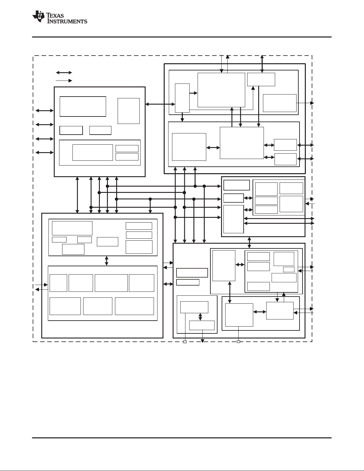
SWCS053-001
Power Subchip (A-D)
Power analog
Power digital
Auxiliary Subchip (A-D)
Audio subchip (A-D)
Interface Subchip(D)
AUDIO digita l
MADCTOP
BCITOP
BCI analog
USB Subchip (A-D)
Card Det 1
Card Det 2
GPIO
TAP
OCP
RTC
RFID
PMC master
PMC slave
LED digital
LED analog
LEDTOP
Device
Clocks
Digital signal(s)
Analog signal(s)
PCM (4)
TDM (4)
StartADC
LedSync
ULPI (12)
UART (2)
Clocks
OCP
SIH_INT
TAP
OCP
Clocks
SIH_INT
Clo cks
TAP
I2C A pad
I2C B pad
Clk In/Out
GPIO pad
SHIFTERS
SIH_INT
OCP
TAP
Clocks
SIH_INT
OCP
TAP
TAP
EEprom
CLED
PIH
Clock
generator
SIH
AUDIO
analog
Audio
PLL
Wrapper
digital
Audio RX amplifiers
Mic amplifiers
Analog volume control
D/A converters
A/D converters
Differential vibrator
Digital mic
interface
Analog and
digital mic
bias
Audio and voice filters
(RX and TX paths)
+
Vibrator control
PCM
interface
TDM/I2S
interface
VBUS –2v..20v
tolerance
Charge
pump
USB
charger
detection
USB Power
supply
USB
precharge
module
USB
digital
(ULPI/
registers
interrupts)
OTG
module
USB2.0
transceiver
Audio loop
control
BCI
digital
USB charger
EXT charger
-control
-status
USB charger
driver
EXT charge
driver
VBAT
removal
discharger
VBAT –2v..20v
tolerance
MADC
digital
state-machine
MADC analog
(SAR-Vref)
Secondary
interrupt handler
SIH
SmartReflex
Vibrator
control (D)
Slave OCP
wrapper
13 MHz/32 kHz
RTC
32 kHz
Clock slicer
Thermal monitor
system
RC oscillator
Power control
(BBS-backup
VRRTC-UVLO)
Power provider
(LDOs-DCDCs)
Power references
(Vref-Iref-BandGap)
OCP SR
TPS65951
www.ti.com
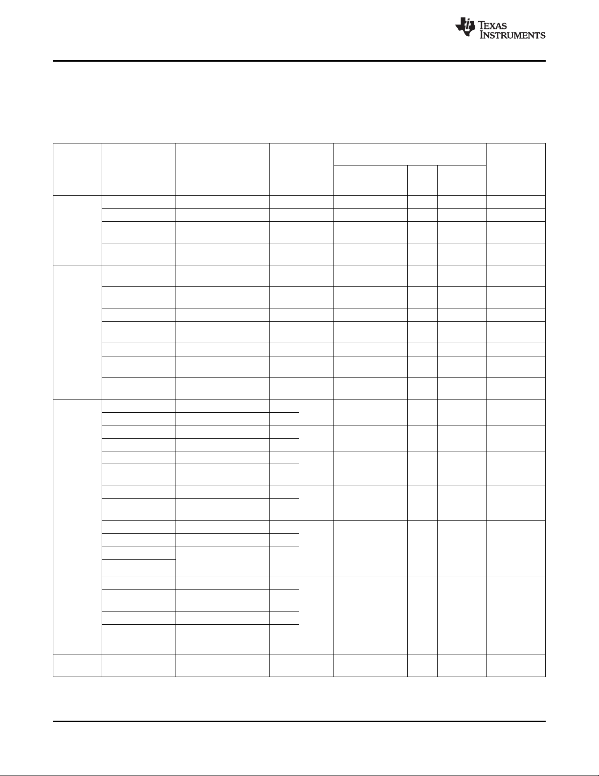
1.1 TPS65951 Block Diagram
SWCS053F –SEPTEMBER 2010–REVISED MAY 2012
Copyright © 2010–2012, Texas Instruments Incorporated Introduction 13
Figure 1-1. TPS65951 Block Diagram
Submit Documentation Feedback
Product Folder Link(s): TPS65951
Page 14
9,60 TYP
0,80
0,80
N
M
L
K
J
H
G
F
E
D
C
B
A
1 2 3 4 5
Bottom View
6 7 8 9 10 11 12 13
SWCS053-002
TPS65951
SWCS053F –SEPTEMBER 2010–REVISED MAY 2012
2 Terminal Description
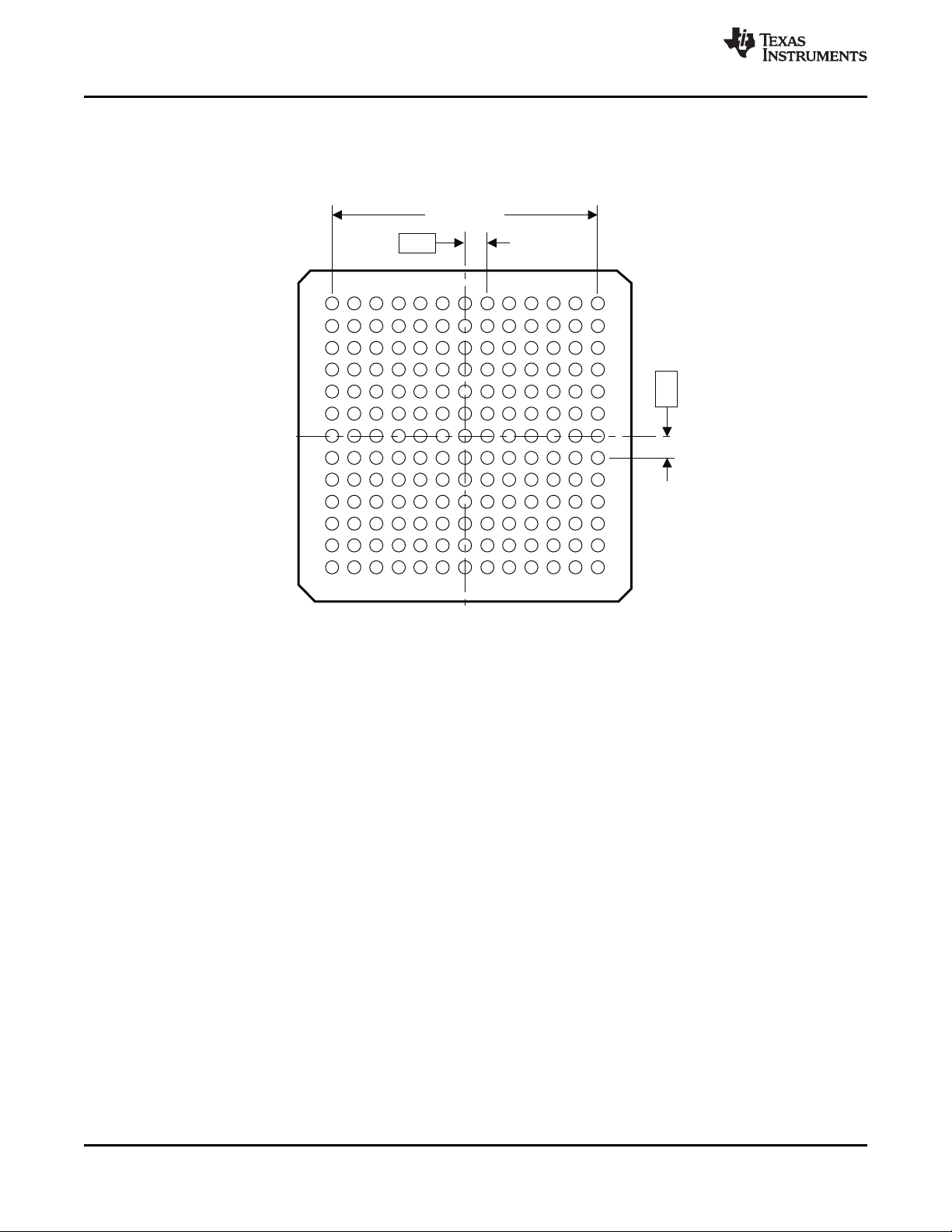
Figure 2-1 illustrates the ball locations for the 169-ball plastic ball grid array (PBGA) package and is used
in conjunction with Table 2-1 to locate signal names and ball grid numbers.
www.ti.com
Figure 2-1. PBGA Bottom View
2.1 Corner Balls
The four corner balls (TEST, TESTV1, TEST.RESET, and TESTV2) are not useable for functional pins.
14 Terminal Description Copyright © 2010–2012, Texas Instruments Incorporated
Submit Documentation Feedback
Product Folder Link(s): TPS65951
Page 15
TPS65951
www.ti.com
SWCS053F –SEPTEMBER 2010–REVISED MAY 2012
2.2 Ball Characteristics
Table 2-1 describes the terminal characteristics and the signals multiplexed on each pin. The following list
describes the table column headers:
1. BALL: ball number(s) associated with each signal(s)
2. PIN NAME: the names of all the signals that are multiplexed on each ball
3. A/D: analog or digital signal
4. TYPE: the terminal type when a particular signal is multiplexed on the terminal
5. REFERENCE LEVEL: the voltage applied to the I/O cell (see Section 6 and Section 8 for values).
6. PU/PD: denotes the presence of an internal pullup or pulldown. Pullups and pulldowns can be enabled
or disabled via software.
7. BUFFER STRENGTH: drive strength of the associated output buffer
8. ESD RAIL: power reference for ESD protection
Table 2-1. Ball Characteristics
REFERENCE PU[6] (kΩ)
BALL PIN A/D TYPE ESD RAIL[8]
[1] NAME[2] [3] [4] VDD
K1 ADCIN0 A I/O ADCIN0 VINTANA1.OUT
G3 ADCIN1 A I/O None VINTANA1.OUT
F4 ADCIN2 A I VINTANA2.OUT VINTANA2.OUT
J5 USBCHRG_ENZ A O VPRECH VPRECH 4
H5 USBCHRG_STAT A I VPRECH VPRECH 65 139
Z
K4 VPROG A I None VPP
L1 VPRECH A O None VPRECH
K6 CHRG_DET_N A O VPRECH VPRECH 4
K12 VREFGND A Power None GND
GND
L5 VBAT A Power AGND VBAT
M8 GPIO.0/CD1 D I/O IO.1P8 IO.1P8 75 100 202 59 100 144 8
JTAG.TDO D I/O IO.1P8 IO.1P8 8
L9 GPIO.1/CD2 D I/O IO.1P8 IO.1P8 75 100 202 59 100 144 2
JTAG.TMS D I IO.1P8 IO.1P8
J3 GPIO.2 D I/O IO.1P8 IO.1P8 156 220 450 59 100 144 2
TEST1 D I/O IO.1P8 IO.1P8 2
L10 GPIO.15 D I/O IO.1P8 IO.1P8 156 220 450 59 100 144 2
TEST2 D I/O IO.1P8 IO.1P8 2
K3 GPIO.6 D I/O IO.1P8 IO.1P8 75 100 202 59 100 144 2
PWM0 D O IO.1P8 IO.1P8 4
TEST3 D I/O IO.1P8 IO.1P8 2
CLKOK
M13 GPIO.7 D I/O IO.1P8 IO.1P8 75 100 202 59 100 144 2
VIBRA.SYNC D I IO.1P8 IO.1P8
PWM1 D O IO.1P8 IO.1P8 4
TEST4 D I/O IO.1P8 IO.1P8 2
L11 START.ADC D I IO.1P8 IO.1P8
E8 SYSEN D Open IO.1P8 IO.1P8 4.7 7.35 10 2
drain/I
F6 CLKEN D O IO.1P8 IO.1P8 2
(3)
LEVEL STRENGTH
RL[5] (mA)[7]
MIN TYP MAX MIN TYP MAX
(4)
PD[6] (kΩ)
(4)
BUFFER
Copyright © 2010–2012, Texas Instruments Incorporated Terminal Description 15
Submit Documentation Feedback
Product Folder Link(s): TPS65951
Page 16
TPS65951
SWCS053F –SEPTEMBER 2010–REVISED MAY 2012
Table 2-1. Ball Characteristics (continued)
BALL PIN A/D TYPE ESD RAIL[8]
[1] NAME[2] [3] [4] VDD
REFERENCE PU[6] (kΩ)
(3)
LEVEL STRENGTH
RL[5] (mA)[7]
MIN TYP MAX MIN TYP MAX
(4)
PD[6] (kΩ)
B13 CLKREQ D I IO.1P8 IO.1P8 60 100 146
B10 INT1 D O IO.1P8 IO.1P8 2
C10 NRESPWRON D O IO.1P8 IO.1P8 2
A11 NRESWARM D I IO.1P8 IO.1P8 2
F7 PWRON D I VBAT.RIGHT VBAT
C11 NSLEEP1 D I IO.1P8 IO.1P8
J13 BOOT0 A/D I/O VPLLA3R.IN VBAT
G10 BOOT1 A/D I/O VPLLA3R.IN VBAT
D8 REGEN D Open VBAT.LEFT VBAT 5.5 8 12 2
Drain
B7 MSECURE D I IO.1P8 IO.1P8
K13 VREF A Power None VREF
G7 AGND A Power None GND
GND
C4 I2C.SR.SDA D I/O IO.1P8 IO.1P8 2.5 3.4 12
B5 VMODE2 D I IO.1P8 IO.1P8 2
I2C.SR.SCL D I/O IO.1P8 IO.1P8 2.5 3.4 12
E5 I2C.CNTL.SDA D I/O IO.1P8 IO.1P8 2.5 3.4 12
D5 I2C.CNTL.SCL D I IO.1P8 IO.1P8 2.5 3.4 12
M1 PCM.VCK D I/O IO.1P8 IO.1P8 2
L4 PCM.VDR D I/O IO.1P8 IO.1P8 2
H8 PCM.VDX D I/O IO.1P8 IO.1P8 2
N12 PCM.VFS D I/O IO.1P8 IO.1P8 2
J4 I2S.CLK D I/O IO.1P8 IO.1P8 2
K2 I2S.SYNC D I/O IO.1P8 IO.1P8 2
H3 I2S.DIN D I IO.1P8 IO.1P8 2
H4 I2S.DOUT D O IO.1P8 IO.1P8 2
D2 MIC.MAIN.P A I VINTANA1.OUT MICBIAS1.OUT
E2 MIC.MAIN.M A I VINTANA1.OUT MICBIAS1.OUT
F5 MIC.SUB.P A I VINTANA1.OUT MICBIAS2.OUT
DIG.MIC.0 A I VINTANA1.OUT VMIC1.OUT
G5 MIC.SUB.M A I VINTANA1.OUT MICBIAS2.OUT
E4 HSMIC.P A I VINTANA1.OUT VINTANA2.OUT
E3 HSMIC.M A I VINTANA1.OUT VINTANA2.OUT
A7 VBAT.LEFT A Power VINTANA1.OUT
B8 IHF.LEFT.P A O VINTANA1.OUT
A8 IHF.LEFT.M A O VINTANA1.OUT
(2)
VBAT
(2)
VBAT
(2)
VBAT
C8 GND.LEFT A Power None GND
GND
A10 VBAT.RIGHT A Power VINTANA1.OUT
B9 IHF.RIGHT.P A O VINTANA1.OUT
A9 IHF.RIGHT.M A O VINTANA1.OUT
(2)
VBAT
(2)
VBAT
(2)
VBAT
C9 GND.RIGHT A Power None GND
GND
C6 EAR.P A O IO.1P8
D6 EAR.M A O IO.1P8
C5 HSOL A O IO.1P8
(2)
(2)
(2)
VINTANA2.OUT
VINTANA2.OUT
VINTANA2.OUT
(4)
www.ti.com
BUFFER
16 Terminal Description Copyright © 2010–2012, Texas Instruments Incorporated
Submit Documentation Feedback
Product Folder Link(s): TPS65951
Page 17
TPS65951
www.ti.com
SWCS053F –SEPTEMBER 2010–REVISED MAY 2012
Table 2-1. Ball Characteristics (continued)
BALL PIN A/D TYPE ESD RAIL[8]
[1] NAME[2] [3] [4] VDD
E6 PreDriv.LEFT A O IO.1P8
VMID A Power IO.1P8
A5 HSOR A O IO.1P8
D7 PreDriv.RIGHT A O IO.1P8
ADCIN7 A I IO.1P8
(2)
(2)
(2)
(2)
(2)
REFERENCE PU[6] (kΩ)
(3)
LEVEL STRENGTH
RL[5] (mA)[7]
VINTANA2.OUT
VINTANA2.OUT
VINTANA2.OUT
VINTANA2.OUT
VINTANA2.OUT
MIN TYP MAX MIN TYP MAX
(4)
PD[6] (kΩ)
E1 AUXL A I VINTANA1.OUT VINTANA2.OUT
F3 AUXR A I VINTANA1.OUT VINTANA2.OUT
B1 MICBIAS1.OUT A Power VINTANA2.OUT VINTANA2.OUT
VMIC1.OUT A Power VINTANA2.OUT VINTANA2.OUT
C1 MICBIAS2.OUT A Power VINTANA2.OUT VINTANA2.OUT
VMIC2.OUT A Power VINTANA2.OUT VINTANA2.OUT
D3 VHSMIC.OUT A Power VINTANA2.OUT VINTANA2.OUT
D1 MICBIAS.GND Power None GND
GND
G4 AVSS1 A Power None GND
GND
K7 AVSS2 A Power None GND
GND
K11 AVSS3 A Power None GND
GND
A6 AVSS4 A Power None GND
GND
K8 ADCIN3 A I VUSB.3P1 VINTANA2.OUT
K9 MANU_BRIX D O IO.1P8 IO.1P8
J6 32KCLKOUT D O IO.1P8 IO.1P8
L12 32KXIN A I VRTC.OUT IO.1P8
L13 32KXOUT A O VRTC.OUT IO.1P8
B11 HFCLKIN A I IO.1P8 IO.1P8
N8 HFCLKOUT D O IO.1P8 IO.1P8
H7 VBUS A Power None VBUS
J7 DP/UART3.RXD A I/O None VBUS 2
J8 DN/UART3.TXD A I/O None VBUS 2
L8 ID A I/O None VBUS 2
J9 UCLK D I/O IO.1P8 IO.1P8 16
K10 STP D I IO.1P8 IO.1P8 75 100 202 59 100 144 16
GPIO.9 D I/O IO.1P8 IO.1P8 2
J10 DIR D O IO.1P8 IO.1P8 75 100 202 59 100 144 16
GPIO.10 D I/O IO.1P8 IO.1P8 2
J11 NXT D O IO.1P8 IO.1P8 75 100 202 59 100 144 16
GPIO.11 D I/O IO.1P8 IO.1P8 2
H11 DATA0 D I/O IO.1P8 IO.1P8 16
UART4.TXD D I IO.1P8 IO.1P8
H10 DATA1 D I/O IO.1P8 IO.1P8 16
UART4.RXD D O IO.1P8 IO.1P8 2
G8 DATA2 D I/O IO.1P8 IO.1P8 16
H9 DATA3 D I/O IO.1P8 IO.1P8 60 100 140 60 100 140 16
GPIO.12 D I/O IO.1P8 IO.1P8 75 100 202 59 100 144 16
(4)
BUFFER
Copyright © 2010–2012, Texas Instruments Incorporated Terminal Description 17
Submit Documentation Feedback
Product Folder Link(s): TPS65951
Page 18
TPS65951
SWCS053F –SEPTEMBER 2010–REVISED MAY 2012
Table 2-1. Ball Characteristics (continued)
BALL PIN A/D TYPE ESD RAIL[8]
[1] NAME[2] [3] [4] VDD
REFERENCE PU[6] (kΩ)
(3)
LEVEL STRENGTH
RL[5] (mA)[7]
MIN TYP MAX MIN TYP MAX
(4)
PD[6] (kΩ)
F9 DATA4 D I/O IO.1P8 IO.1P8 75 100 202 59 100 144 16
GPIO.14 D I/O IO.1P8 IO.1P8 2
F8 DATA5 D I/O IO.1P8 IO.1P8 75 100 202 59 100 144 16
GPIO.3 D I/O IO.1P8 IO.1P8 2
E10 DATA6 D I/O IO.1P8 IO.1P8 75 100 202 59 100 144 16
GPIO.4 D I/O IO.1P8 IO.1P8 2
E11 DATA7 D I/O IO.1P8 IO.1P8 75 100 202 59 100 144 16
GPIO.5 D I/O IO.1P8 IO.1P8 2
N13 TEST.RESET A/D I None VBAT 30 50 70
N1 TESTV1 A I/O None VBAT
A13 TESTV2 A I/O IO.1P8
(2)
VINTANA2.OUT
A1 TEST D I IO.1P8 IO.1P8 60 100 146
B12 JTAG.TDI/ D I IO.1P8 IO.1P8
BERDATA
D11 JTAG.TCK/ D I IO.1P8 IO.1P8
BERCLK
M5 CP.IN A Power None VBAT/VBUS
N6 CP.CAPP A O VINTUSB1P8.OU CP.CAPP
N5 CP.CAPM A O VINTUSB1P8.OU CP.CAPM
(2)
T
(2)
T
K5 CP.GND A Power None GND
GND
L6 VUSBIN.CPOUT A Power None VBAT
N7 VBAT.USB A Power None VBAT
L7 VUSB.3P1 A Power VUSB.3P1 VUSB.3P1
H1 VAUX12S.IN A Power None VBAT
J2 VAUX1.OUT A Power VAUX1.OUT VAUX1.OUT
J1 VAUX2.OUT A Power VAUX2.OUT VAUX2.OUT
F13 VPLLA3R.IN A Power AGND VBAT
G12 VRTC.OUT A Power None VRTC.OUT
G9 VPLL1.OUT A Power VPPL1.OUT VPLL1.OUT
G13 VPLL2.OUT A Power VPLL2.OUT VPLL2.OUT
F12 VAUX3.OUT A Power VAUX3.OUT VAUX3.OUT
A2 VAUX4.IN A Power None VBAT
B3 VAUX4.OUT A Power VAUX4.OUT VAUX4.OUT
C2 VMMC1.IN A Power None VBAT
B2 VMMC1.OUT A Power VMMC1.OUT VMMC1.OUT
A4 VMMC2.IN A Power None VBAT
B4 VMMC2.OUT A Power VMMC2.OUT VMMC2.OUT
G2 VSL.OUT A Power IO.1P8
(2)
VSL.OUT
M6 VINTUSB1P5.OU A Power None VINTUSB1P5.OU
T T
M7 VINTUSB1P8.OU A Power None VINTUSB1P8.OU
T T
G1 VDAC.IN A Power None VBAT
H2 VDAC.OUT A Power VDAC.OUT VDAC.OUT
H13 VINT.IN A Power None VBAT
(4)
www.ti.com
BUFFER
18 Terminal Description Copyright © 2010–2012, Texas Instruments Incorporated
Submit Documentation Feedback
Product Folder Link(s): TPS65951
Page 19
TPS65951
www.ti.com
SWCS053F –SEPTEMBER 2010–REVISED MAY 2012
Table 2-1. Ball Characteristics (continued)
REFERENCE PU[6] (kΩ)
BALL PIN A/D TYPE ESD RAIL[8]
[1] NAME[2] [3] [4] VDD
(3)
LEVEL STRENGTH
RL[5] (mA)[7]
MIN TYP MAX MIN TYP MAX
F2 VINTANA1.OUT A Power None VINTANA1.OUT
B6 VINTANA2.OUT A Power VINTANA2.OUT VINTANA2.OUT
F1 VINTANA2.OUT A Power VINTANA2.OUT VINTANA2.OUT
H12 VINTDIG.OUT A Power None VINTDIG.OUT
E12 VDD1.IN A Power VINTDIG.OUT
E13 VDD1.IN A Power VINTDIG.OUT
(2)
VBAT
(2)
VBAT
D12 VDD1.SW A O VDD1.IN VBAT
D13 VDD1.SW A O VDD1.IN VBAT
D10 VDD1.FB A I None
C12 VDD1.GND A Power None GND
GND
C13 VDD1.GND A Power None GND
GND
N9 VDD2.IN A Power VINTDIG.OUT
M9 VDD2.IN A Power VINTDIG.OUT
(2)
VBAT
(2)
VBAT
M12 VDD2.FB A I None
M10 VDD2.SW A O VDD2.IN VBAT
N10 VDD2.SW A O VDD2.IN VBAT
M11 VDD2.GND A Power None GND
GND
N11 VDD2.GND A Power None GND
GND
M4 VIO.IN A Power VINTDIG.OUT
N4 VIO.IN A Power VINTDIG.OUT
(2)
VBAT
(2)
VBAT
L2 VIO.FB A I None
M3 VIO.SW A O VIO.IN VBAT
N3 VIO.SW A O VIO.IN VBAT
N2 VIO.GND A Power None GND
GND
M2 VIO.GND A Power None GND
GND
L3 VIO.GND A Power None GND
GND
J12 BKBAT A Power BKBAT VBACK
E7 IO.1P8 A Power None IO.1P8
G11 DGND A Power None GND
GND
F10 LEDGND A Power None GND
GND
A12 GPIO.13 D I/O IO.1P8 IO.1P8 75 100 202 59 100 144
LEDSYNC D I IO.1P8 IO.1P8
E9 LEDA A Open IO.1P8
(2)
VBAT
Drain
VIBRA.P A Open IO.1P8
(2)
VBAT
Drain
F11 LEDB A Open IO.1P8
(2)
VBAT
Drain
VIBRA.M A Open IO.1P8
(2)
VBAT
Drain
D9 VBATVIBRA A Power IO.1P8
(2)
VBAT
(4)
PD[6] (kΩ)
(4)
BUFFER
Copyright © 2010–2012, Texas Instruments Incorporated Terminal Description 19
Submit Documentation Feedback
Product Folder Link(s): TPS65951
Page 20
TPS65951
SWCS053F –SEPTEMBER 2010–REVISED MAY 2012
Table 2-1. Ball Characteristics (continued)
REFERENCE PU[6] (kΩ)
BALL PIN A/D TYPE ESD RAIL[8]
[1] NAME[2] [3] [4] VDD
C3 GPIO.16 D I/O IO.1P8 IO.1P8 75 100 202 59 100 144
DIG.MIC.CLK0 D O IO.1P8 IO.1P8
(1) To avoid reflection on this pin due to impedance mismatch, a serial resistance of 33 Ω needs to be added.
(2) VDD rail used as bias in ESD protection during functional mode.
(3) AGND is used as ESD Ground for all PADs.
(4) PUs/PDs are enabled when TPS65952 is in any other state than NO SUPPLY
(3)
LEVEL STRENGTH
RL[5] (mA)[7]
MIN TYP MAX MIN TYP MAX
(4)
PD[6] (kΩ)
(4)
2.2.1 ESD Electrical Parameters
ESD conditions for CDM and HBM listed in Table 2-2.
Table 2-2. ESD Electrical Parameters
PARAMETER TEST CONDITIONS MIN TYP MAX UNIT
CDM stress voltage All pads 500 V
HBM stress voltage All pads 2000 V
www.ti.com
BUFFER
20 Terminal Description Copyright © 2010–2012, Texas Instruments Incorporated
Submit Documentation Feedback
Product Folder Link(s): TPS65951
Page 21
SWCS053-092
12345678910111213
A
TEST
VAUX4.IN
Reserved
VMMC2.IN
HSOR
AVSS4
VBAT.LEFT
IHF.LEFT.M
IHF.RIGHT.M
VBAT.RIGHT
NRESWARM
LEDSYNC/
GPIO.13
TESTV2
A
B
MICBIAS1.
OUT/
VMIC1 OUT.
VMMC1.OUT
VAUX4.OUT
VMMC2.OUT
VMODE2/
I2C.SR.SCL
VINTANA2
.OUT
MSECURE
IHF.LEFT.P
IHF.RIGHT.P
INT1
HFCLKIN
JTAG.TDI/
BERDATA
CLKREQ
B
C
MICBIAS2.
OUT/
VMIC2 OUT.
VMMC1.IN
GPIO16/
DIG.MIC.
CLK0
I2C.SR.SDA
HSOL
EAR.P
Reserved
GND.LEFT
GND.RIGHT
NRESPWRON
NSLEEP1
VDD1.GND
VDD1.GND
C
D
MICBIAS.
GND
MIC.MAIN.P
VHSMIC.OUT
Reserved
I2C.CNTL.
SCL
EAR.M
PreDriv.
RIGHT/
ADCIN7
REGEN
VBATVIBRA
VDD1.FB
JTAG.TCK/
BERCLK
VDD1.SW
VDD1.SW
D
E
AUXL
MIC.MAIN.M
HSMIC.M
HSMIC.P
I2C.CNTL.
SDA
PreDriv
.LEFT/
VMID
IO.1P8
SYSEN
LEDA/
VIBRA.P
DATA6/
GPIO.4
DATA7/
GPIO.5
VDD1.IN
VDD1.IN
E
F
VINTANA2.
OUT
VINTANA1.
OUT
AUXR
ADCIN2
MIC.SUB./
DIG.MIC.0
CLKEN
PWRON
DATA5/
GPIO.3
DATA4/
GPIO.14
LEDGND
LEDB/
VIBRA.M
VAUX3.OUT
VPLLA3R.IN
F
G
VDAC.IN
VSL.OUT
ADCIN1
AVSS1
MIC.SUB.M
Reserved
AGND
DATA2
VPPL1.OUT
BOOT1
DGND
VRTC.OUT
VPLL2.OUT
G
H
VAUX12S.IN
VDAC.OUT
I2S.DIN
I2S.DOUT
USBCHRG
_STATZ
Reserved
VBUS
PCM.VDX
DATA3/
GPIO.12
DATA1/
UART4.RXD
DATA0/
UART4.TXD
VINTDIG.OUT
VINT.IN
H
J
VAUX2.OUT
VAUX1.OUT
GPIO.2/
TEST1
I2S.CLK
USBCHRG
_ENZ
32KCLKOUT
DP/UART3.
RXD
DN/
UART3.TXD
UCLK
DIR/
GPIO.10
NXT/
GPIO.11
BKBAT
BOOT0
J
K
ADCIN0
I2S.SYNC
GPIO6/
CLKOK/
PWM0/
TEST3
VPROG
CP.GND
CHRG_
DET_N
AVSS2
ADCIN3
MANU_BRIX
STP/GPIO.9
AVSS3
VREFGND
VREF
K
L
VPRECH
VIO.FB
VIO.GND
PCM.VDR
VBAT
VUSBIN.
CPOUT
VUSB.3P1
ID
GPIO.1/CD2/
JTAG.TMS
GPIO.15/
TEST2
START.ADC
32KXIN
32KXOUT
L
M
PCM.VCK
VIO.GND
VIO.SW
VIO.IN
CP.IN
VINTUSB1
P5.OUT
VINTUSB1
P8.OUT
GPIO.0/CD1/
JTAG.TD0
VDD2.IN
VDD2.SW
VDD2.GND
VDD2.FB
GPIO.7/
VIBRA.SY
NC.PWM1/
TEST4
M
N
TESTV1
VIO.GND
VIO.SW
VIO.IN
CP.CAPM
CP.CAPP
VBAT.USB
HFCLKOUT
VDD2.IN
VDD2.SW
VDD2.GND
PCM.VFS
TEST.RES
ET
N
12345678910111213
TPS65951
www.ti.com
2.3 Ball Placement (Top View)
SWCS053F –SEPTEMBER 2010–REVISED MAY 2012
Figure 2-2. Top View
Copyright © 2010–2012, Texas Instruments Incorporated Terminal Description 21
Submit Documentation Feedback
Product Folder Link(s): TPS65951
Page 22
TPS65951
SWCS053F –SEPTEMBER 2010–REVISED MAY 2012
www.ti.com
2.4 Signal Description
Table 2-3 provides a description of the signals on the TPS65951; some signals are available on multiple
pins.
Table 2-3. Signal Description
CONFIGURATION BY DEFAULT AFTER
MODULE SIGNAL NAME DESCRIPTION TYPE BALLS
ADC ADCIN0 Battery type I/O K1 ADCIN0 I Floating
ADCIN1 Battery temperature I/O G3 ADCIN1 I Floating
ADCIN2 General-purpose ADC I F4 ADCIN2 I Floating
ADCIN3 General-purpose ADC I K8 ADCIN3 I Floating
Charger VPROG EEPROM programming I K4 VPROG I GND
VPRECH Precharge regulator O L1 VPRECH O Cap to GND
VBAT Battery voltage sensing Power L5 VBAT Power VBAT
CHRG_DET_N USB Charger Detection O K6 CHRG_DET_N O Floating
USBCHRG_ENZ USB charger enable Z O J5 USBCHRG_ENZ O Floating
USBCHRG_STAT USB charger status I H5 USBCHRG_STAT I PU Floating
Z Z
MANU_BRIX Battery Removal O K9 MANU_BRIX O Floating
GPIOs / GPIO.0/CD1 GPIO0/card detection 1 I/O M8 GPIO.0 I PD Floating
JTAG
START. START.ADC ADC conversion request I L11 START.ADC I GND
ADC
JTAG.TDO JTAG test data output I/O
GPIO.1/CD2 GPIO1/card detection 2 I/O L9 GPIO.1 I PD Floating
JTAG.TMS JTAG test mode state I
GPIO.2 GPIO2 I/O J3 GPIO.2 I PD Floating
TEST1 TEST1 pin used in test I/O
GPIO.15 GPIO15 I/O L10 GPIO.15 I PD Floating
TEST2 TEST2 pin used in test I/O
GPIO.6 GPIO6 I/O K3 GPIO.6 I PD Floating
PWM0 Pulse width driver 0 O
TEST3 TEST3 pin used in test I/O
CLKOK
GPIO.7 GPIO.7 I/O M13 GPIO.7 I PD Floating
VIBRA.SYNC Vibrator on-off I
PWM1 Pulse width driver O
TEST4 TEST4 pin used in test I/O
input
input 3
voltage
output
(100 mA/500 mA)
Indicator
mode only
mode only
mode only (controlled by
JTAG)
synchronization
mode only (controlled by
JTAG)
RESET RELEASED
INTERNAL
SIGNAL TYPE PULL OR
NOT
NOT USED
FEATURES
(1)
(3)
22 Terminal Description Copyright © 2010–2012, Texas Instruments Incorporated
Submit Documentation Feedback
Product Folder Link(s): TPS65951
Page 23
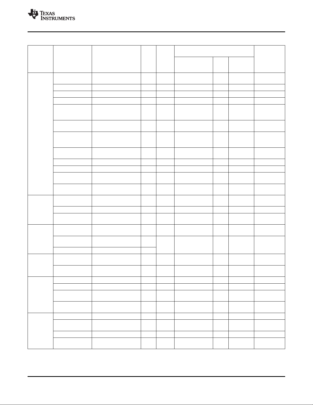
TPS65951
www.ti.com
SWCS053F –SEPTEMBER 2010–REVISED MAY 2012
Table 2-3. Signal Description (continued)
CONFIGURATION BY DEFAULT AFTER
MODULE SIGNAL NAME DESCRIPTION TYPE BALLS
CONTROL SYSEN System enable output Open E8 SYSEN OD PU Floating
drain/I
CLKEN Clock enable O F6 CLKEN O Floating
CLKREQ Clock request I B13 CLKREQ I PD GND
INT1 Output interrupt line 1 O B10 INT1 O Floating
NRESPWRON Output control the O C10 NRESPWRON O Floating
NRESPWRON of the
application processor
NRESWARM Input, detect user action I A11 NRESWARM I GND
on the reset button
PWRON Input, detect a control I F7 PWRON I VBAT
command to start or stop
the system
NSLEEP1 Sleep request from I C11 NSLEEP1 I GND
device 1
BOOT0 Boot pin 0 I J13 BOOT0 I PD Not Applicable
BOOT1 Boot pin 1 I G10 BOOT1 I PD Not Applicable
REGEN Enable signal for Open D8 REGEN OD PU Floating
external LDO Drain
MSECURE Security and digital I B7 MSECURE I IO.1P8
rights management
VREF VREFGND Reference voltage Power K12 VREFGND Power GND
ground GND GND
VREF Reference voltage Power K13 VREF Power Not Applicable
AGND Analog ground for Power G7 AGND Power GND
reference voltage GND GND
I2C I2C.SR.SDA SmartReflex I2C data I/O C4 Signal not Floating
SmartReflex functional
VMODE2 Digital voltage scaling I B5 VMODE2 I GND
linked with VDD2
I2C.SR.SCL SmartReflex I2C data I/O
I2C I2C.CNTL.SDA General-purpose I2C I/O E5 I2C.CNTL.SDA IO PU Not Applicable
data
I2C.CNTL.SCL General-purpose I2C I/O D5 I2C.CNTL.SCL IO PU Not Applicable
clock
PCM PCM.VCK Data clock (voice port) I/O M1 PCM.VCK IO Floating
PCM.VDR Data receive (voice port) I/O L4 PCM.VDR IO GND
PCM.VDX Data transmit (voice I/O H8 PCM.VDX IO Floating
port)
PCM.VFS Frame synchronization I/O N12 PCM.VFS IO Floating
(voice port)
TDM I2S.CLK Clock signal (audio port) I/O J4 I2S.CLK IO Floating
I2S.SYNC Synchronization signal I/O K2 I2S.SYNC IO Floating
(audio port)
I2S.DIN Data receive (audio port) I H3 I2S.DIN I GND
I2S.DOUT Data transmit (audio O H4 I2S.DOUT O Floating
port)
RESET RELEASED
INTERNAL
SIGNAL TYPE PULL OR
NOT
(2)
NOT USED
FEATURES
(1)
Copyright © 2010–2012, Texas Instruments Incorporated Terminal Description 23
Submit Documentation Feedback
Product Folder Link(s): TPS65951
Page 24
TPS65951
SWCS053F –SEPTEMBER 2010–REVISED MAY 2012
www.ti.com
Table 2-3. Signal Description (continued)
CONFIGURATION BY DEFAULT AFTER
MODULE SIGNAL NAME DESCRIPTION TYPE BALLS
ANA.MIC MIC.MAIN.P Main microphone left I D2 MIC.MAIN.P I Cap to GND
input (P)
MIC.MAIN.M Main microphone left I E2 MIC.MAIN.M I Cap to GND
input (M)
MIC.SUB.P Main microphone right I F5 MIC.SUB.P I Cap to GND
input (P)
DIG.MIC.0 Digital microphone 0 I
input data
MIC.SUB.M Main microphone right I G5 MIC.SUB.M I Cap to GND
input (M)
Headset HSMIC.P Headset microphone I E4 HSMIC.P I Cap to GND
Microphone input (P)
HSMIC.M Headset microphone I E3 HSMIC.M I Cap to GND
input (M)
Hands-Free VBAT.LEFT Battery voltage input Power A7 VBAT.LEFT Power VBAT
IHF.LEFT.P Hands-free speaker O B8 IHF.LEFT.P O Floating
output left (P)
IHF.LEFT.M Hands-free speaker O A8 IHF.LEFT.M O Floating
output left (M)
GND.LEFT GND Power C8 GND.LEFT Power GND
GND GND
VBAT.RIGHT Battery voltage input Power A10 VBAT.RIGHT Power VBAT
GND.RIGHT GND Power C9 GND.RIGHT Power GND
GND GND
IHF.RIGHT.P Hands-free speaker O B9 IHF.RIGHT.P O Floating
output right (P)
IHF.RIGHT.M Hands-free speaker O A9 IHF.RIGHT.M O Floating
output right (M)
Earpiece EAR.P Earpiece output O C6 EAR.P O Floating
differential output (P)
EAR.M Earpiece output O D6 EAR.M O Floating
differential output (M)
Headset HSOL Differential/single-ended O C5 HSOL O Floating
headset left output
PreDriv.LEFT Predriver output left P for O E6 VMID Power Floating
external class D
amplifier
VMID Power
HSOR Differential/single-ended O A5 HSOR O Floating
headset right output (P)
PreDriv.RIGHT Predriver output right P O D7 ADCIN7 I GND
for external class D
amplifier
ADCIN7 General-purpose ADC I
input 7
AUX Input AUXL Auxiliary audio input left I E1 AUXL I Cap to GND
AUXR Auxiliary audio input I F3 AUXR I Cap to GND
right
RESET RELEASED
INTERNAL
SIGNAL TYPE PULL OR
NOT
NOT USED
FEATURES
(1)
24 Terminal Description Copyright © 2010–2012, Texas Instruments Incorporated
Submit Documentation Feedback
Product Folder Link(s): TPS65951
Page 25
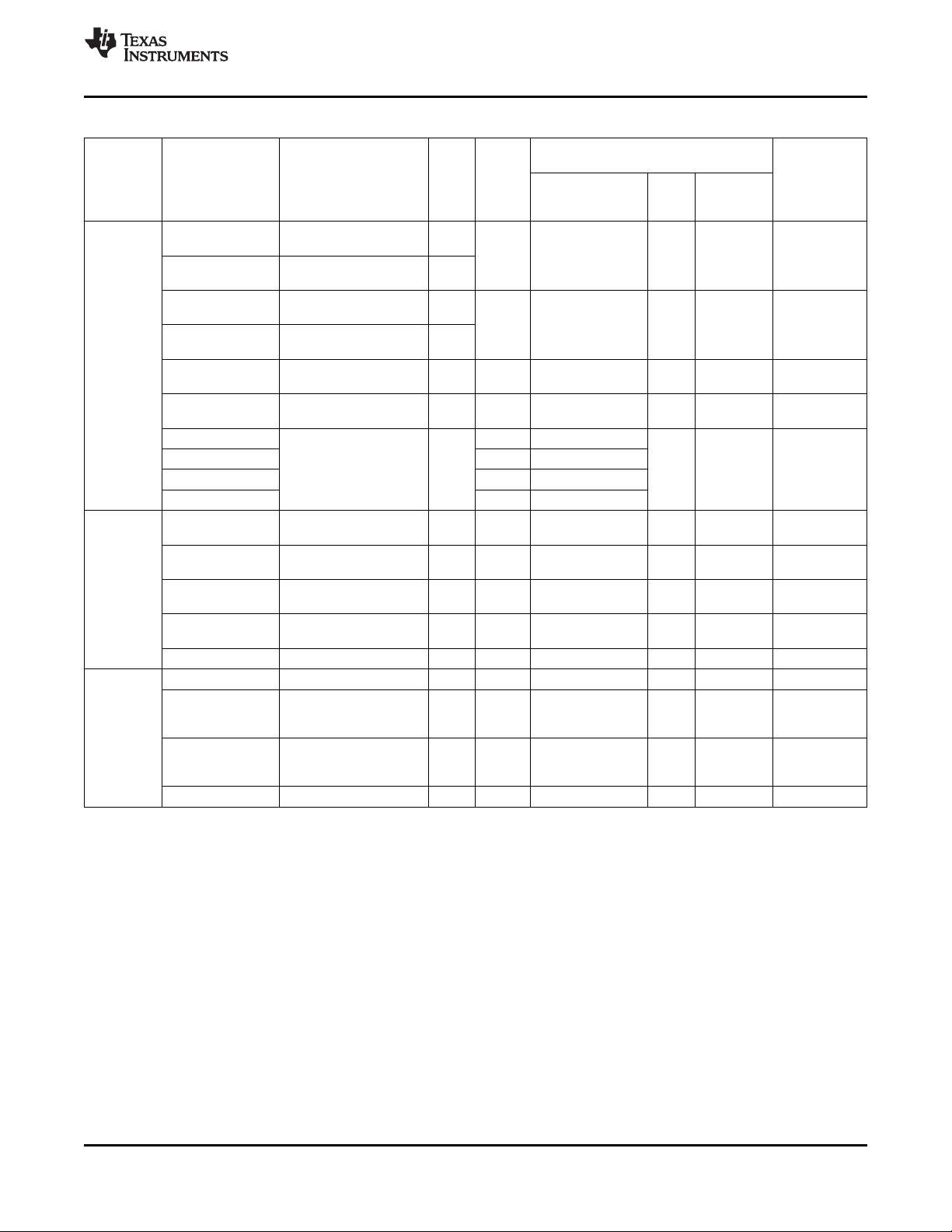
TPS65951
www.ti.com
SWCS053F –SEPTEMBER 2010–REVISED MAY 2012
Table 2-3. Signal Description (continued)
CONFIGURATION BY DEFAULT AFTER
MODULE SIGNAL NAME DESCRIPTION TYPE BALLS
VMIC Bias MICBIAS1.OUT Analog microphone bias Power B1 MICBIAS1.OUT Power Floating
VMIC1.OUT Digital microphone Power
MICBIAS2.OUT Analog microphone bias Power C1 MICBIAS2.OUT Power Floating
VMIC2.OUT Digital microphone Power
VHSMIC.OUT Headset microphone Power D3 VHSMIC.OUT Power Floating
MICBIAS.GND Dedicated ground for Power D1 MICBIAS.GND Power GND
AVSS1 Analog ground Power G4 AVSS1 Power GND
AVSS2 K7 AVSS2
AVSS3 K11 AVSS3
AVSS4 A6 AVSS4
CLOCK 32KCLKOUT Buffered output of the O J6 32KCLKOUT O Floating
32KXIN Input of the 32-kHz I L12 32KXIN I Not Applicable
32KXOUT Output of the 32-kHz O L13 32KXOUT O Floating
HFCLKIN Input of the digital (or I B11 HFCLKIN I Not Applicable
HFCLKOUT High-speed clock output O N8 HFCLKOUT O Floating
USB PHY VBUS VBUS power rail Power H7 VBUS Power Not Applicable
DP/ UART3.RXD USB data P/USB car-kit I/O J7 DP/UART3.RXD IO Not Applicable
DN/ UART3.TXD USB data N/USB car-kit I/O J8 DN/UART3.TXD IO Not Applicable
ID USB ID I/O L8 ID IO Floating
1
power supply 1
2
power supply 2
bias
microphones GND GND
GND GND
32-kHz digital clock
oscillator
oscillator
sine) high-speed clock
receive data/UART3
receive data
transmit data/UART3
transmit data
RESET RELEASED
INTERNAL
SIGNAL TYPE PULL OR
NOT
NOT USED
FEATURES
(1)
Copyright © 2010–2012, Texas Instruments Incorporated Terminal Description 25
Submit Documentation Feedback
Product Folder Link(s): TPS65951
Page 26
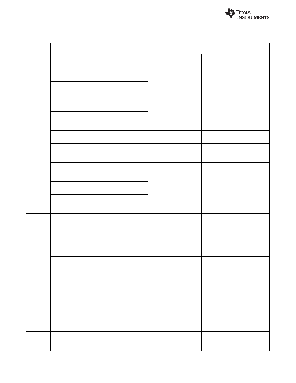
TPS65951
SWCS053F –SEPTEMBER 2010–REVISED MAY 2012
www.ti.com
Table 2-3. Signal Description (continued)
CONFIGURATION BY DEFAULT AFTER
MODULE SIGNAL NAME DESCRIPTION TYPE BALLS
ULPI UCLK High-speed USB clock I/O J9 UCLK O Floating
STP High-speed USB stop I K10 STP I PU Floating
GPIO.9 GPIO.9 I/O
DIR High-speed USB O J10 DIR O Floating
direction
GPIO.10 GPIO.10 I/O
NXT High-speed USB next O J11 NXT O Floating
GPIO.11 GPIO.11 I/O
DATA0 High-speed USB Data0 I/O H11 DATA0 O Floating
UART4.TXD UART4.TXD I
DATA1 High-speed USB Data1 I/O H10 DATA1 O Floating
UART4.RXD UART4.RXD O
DATA2 High-speed USB Data2 I/O G8 DATA2 O Floating
DATA3 High-speed USB Data3 I/O H9 DATA3 O Floating
GPIO.12 GPIO.12 I/O
DATA4 High-speed USB Data4 I/O F9 DATA4 O Floating
GPIO.14 GPIO.14 I/O
DATA5 High-speed USB Data5 I/O F8 DATA5 O Floating
GPIO.3 GPIO.3 I/O
DATA6 High-speed USB Data6 I/O E10 DATA6 O Floating
GPIO.4 GPIO.4 I/O
DATA7 High-speed USB Data7 I/O E11 DATA7 O Floating
GPIO.5 GPIO.5 I/O
TEST TEST.RESET Reset T2 device (except I N13 TEST.RESET I PD GND
power state-machine)
TESTV1 Analog test I/O N1 TESTV1 IO Floating
TESTV2 Analog test I/O A13 TESTV2 IO Floating
TEST Selection between JTAG I A1 TEST I PD Floating
mode and application
mode for JTAG/GPIOs
(with PU or PD)
JTAG.TDI/ JTAG.TDI/BERDATA I B12 JTAG.TDI/ I GND
BERDATA BERDATA
JTAG.TCK/ JTAG.TCK/BERCLK I D11 JTAG.TCK/ I GND
BERCLK BERCLK
USB CP CP.IN Charge pump input Power M5 CP.IN Power VBAT
voltage
CP.CAPP Charge pump flying O N6 CP.CAPP O Floating
capacitor P
CP.CAPM Charge pump flying O N5 CP.CAPM O Floating
capacitor M
VUSBIN.CPOUT Char pump output L6 Power
USBLDO3P3 input
CP.GND Charge pump ground Power K5 CP.GND Power GND
GND GND
VBAT.USB VBAT.USB USB LDOs Power N7 VBAT.USB Power VBAT
(VINTUSB1P5,
VINTUSB1P8,
VUSB.3P1) VBAT
RESET RELEASED
INTERNAL
SIGNAL TYPE PULL OR
NOT
NOT USED
FEATURES
(1)
26 Terminal Description Copyright © 2010–2012, Texas Instruments Incorporated
Submit Documentation Feedback
Product Folder Link(s): TPS65951
Page 27
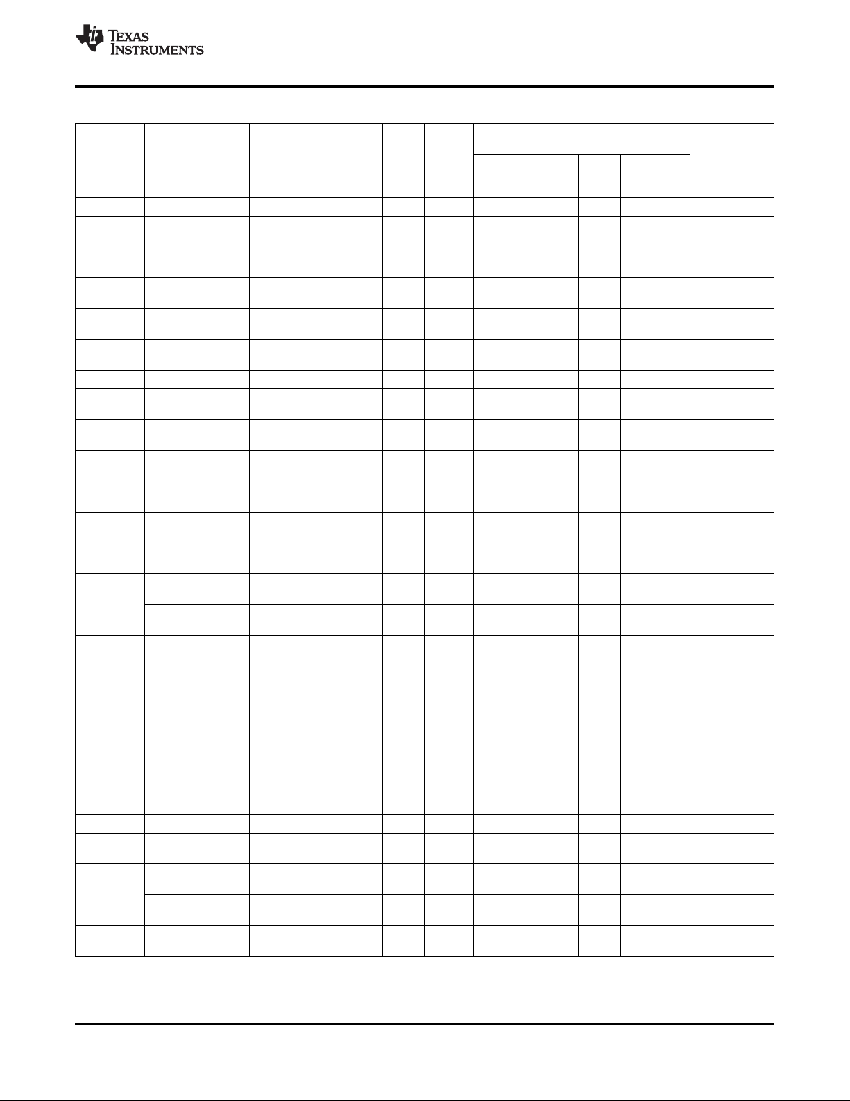
TPS65951
www.ti.com
SWCS053F –SEPTEMBER 2010–REVISED MAY 2012
Table 2-3. Signal Description (continued)
CONFIGURATION BY DEFAULT AFTER
MODULE SIGNAL NAME DESCRIPTION TYPE BALLS
USB.LDO VUSB.3P1 USB LDO output Power L7 VUSB.3P1 Power Not Applicable
VAUX1 VAUX12S.IN VAUX1/VAUX2 LDO Power H1 VAUX12S.IN Power VBAT
input voltage
VAUX1.OUT VAUX1 LDO output Power J2 VAUX1.OUT Power Floating
voltage
VAUX2 VAUX2.OUT VAUX2 LDO output Power J1 VAUX2.OUT Power Floating
voltage
VPLLA3R VPLLA3R.IN Input for VPLL1, VPLL2, Power F13 VPLLA3R.IN Power VBAT
VAUX3, VRTC LDOs
VRTC VRTC.OUT VRTC internal LDO Power G12 VRTC.OUT Power Not Applicable
output (internal use only)
VPLL1 VPLL1.OUT LDO output voltage Power G9 VPLL1.OUT Power Floating
VPLL2 VPLL2.OUT Output voltage of the Power G13 VPLL2.OUT Power Floating
regulator
VAUX3 VAUX3.OUT VAUX3 LDO output Power F12 VAUX3.OUT Power Floating
voltage
VAUX4 VAUX4.IN VAUX4 LDO input Power A2 VAUX4.IN Power VBAT
voltage
VAUX4.OUT VAUX4 LDO output Power B3 VAUX4.OUT Power Floating
voltage
VMMC1 VMMC1.IN VMMC1 LDO input Power C2 VMMC1.IN Power VBAT
voltage
VMMC1.OUT VMMC1 LDO output Power B2 VMMC1.OUT Power Floating
voltage
VMMC2 VMMC2.IN VMMC2 LDO input Power A4 VMMC2.IN Power VBAT
voltage
VMMC2.OUT VMMC2 LDO output Power B4 VMMC2.OUT Power Floating
voltage
VSL VSL.OUT CHARGING led output Power G2 VSL.OUT Power Floating
VINTUSB1 VINTUSB1P5.OUT VINTUSB1P5 internal Power M6 VINTUSB1P5. Power Floating
P5 LDO output (internal use OUT
only)
VINTUSB1 VINTUSB1P8.OUT VINTUSB1P8 internal Power M7 VINTUSB1P8. Power Floating
P8 LDO output (internal use OUT
only)
Video DAC VDAC.IN Input for VDAC, Power G1 VDAC.IN Power VBAT
VINTANA1, and
VINTANA2 LDOs
VDAC.OUT Output voltage of the Power H2 VDAC.OUT Power Floating
regulator
VINT VINT.IN Input for VINTDIG LDO Power H13 VINT.IN Power VBAT
VINTANA1 VINTANA1.OUT VINTANA1 internal LDO Power F2 VINTANA1.OUT Power Not Applicable
output (internal use only)
VINTANA2 VINTANA2.OUT VINTANA2 internal LDO Power B6 VINTANA2.OUT Power Not Applicable
output (internal use only)
VINTANA2.OUT VINTANA2 internal LDO Power F1 VINTANA2.OUT Power Not Applicable
output (internal use only)
VINTDIG VINTDIG.OUT VINTDIG internal LDO Power H12 VINTDIG.OUT Power Not Applicable
output (internal use only)
RESET RELEASED
INTERNAL
SIGNAL TYPE PULL OR
NOT
NOT USED
FEATURES
(1)
Copyright © 2010–2012, Texas Instruments Incorporated Terminal Description 27
Submit Documentation Feedback
Product Folder Link(s): TPS65951
Page 28
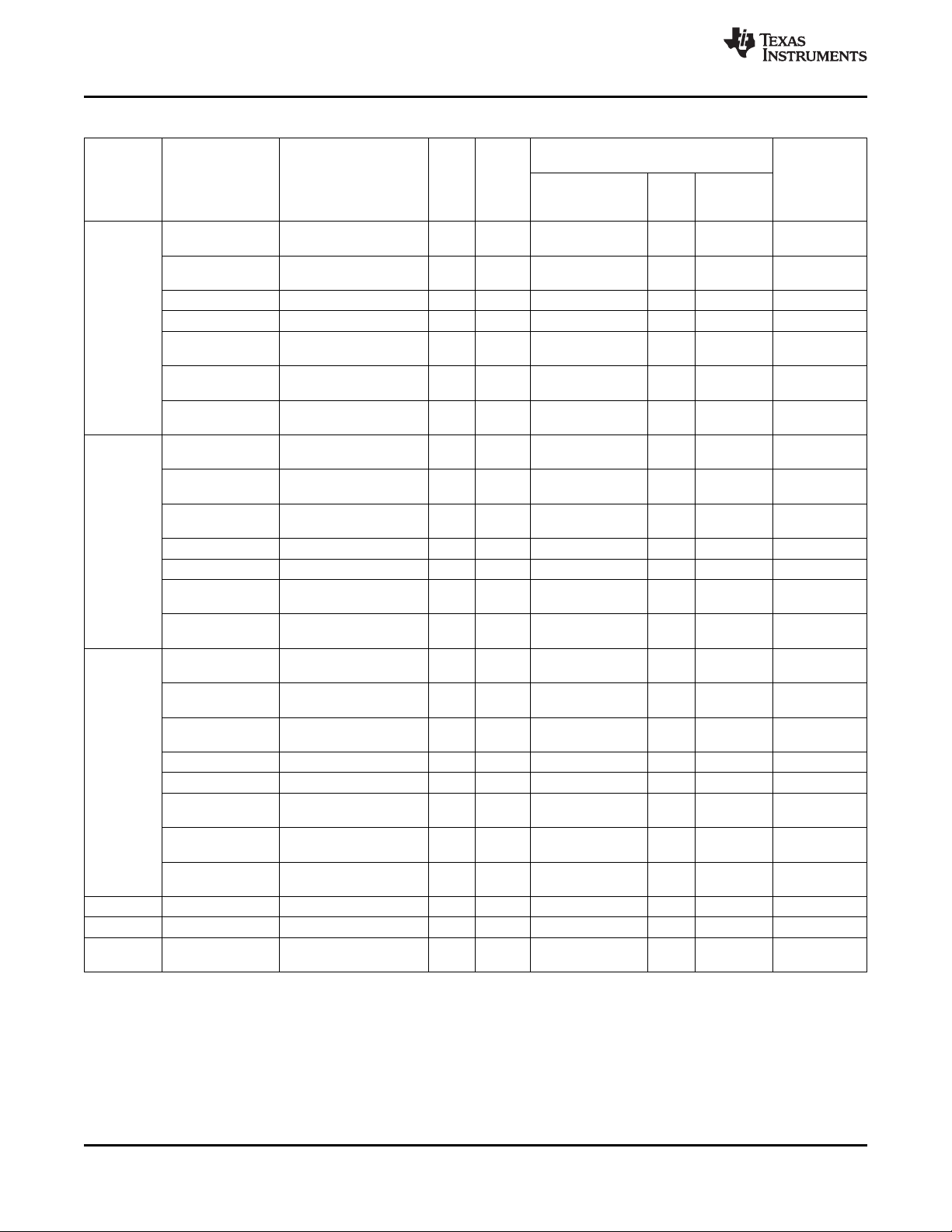
TPS65951
SWCS053F –SEPTEMBER 2010–REVISED MAY 2012
www.ti.com
Table 2-3. Signal Description (continued)
CONFIGURATION BY DEFAULT AFTER
MODULE SIGNAL NAME DESCRIPTION TYPE BALLS
VDD1 VDD1.IN VDD1 DC-DC input Power E12 VDD1.IN Power VBAT
voltage
VDD1.IN VDD1 DC-DC input Power E13 VDD1.IN Power VBAT
voltage
VDD1.SW VDD1 DC-DC switch O D12 VDD1.SW O Floating
VDD1.SW VDD1 DC-DC switch O D13 VDD1.SW O Floating
VDD1.FB VDD1 DC-DC output I D10 VDD1.FB I GND
voltage (feedback)
VDD1.GND VDD1 DC-DC ground Power C12 VDD1.GND Power GND
GND GND
VDD1.GND VDD1 DC-DC ground Power C13 VDD1.GND Power GND
GND GND
VDD2 VDD2.IN VDD2 DC-DC input Power N9 VDD2.IN Power VBAT
voltage
VDD2.IN VDD2 DC-DC input Power M9 VDD2.IN Power VBAT
voltage
VDD2.FB VDD2 DC-DC output I M12 VDD2.FB I GND
voltage (feedback)
VDD2.SW VDD2 DC-DC switch O M10 VDD2.SW O Floating
VDD2.SW VDD2 DC-DC switch O N10 VDD2.SW O Floating
VDD2.GND VDD2 DC-DC ground Power M11 VDD2.GND Power GND
GND GND
VDD2.GND VDD2 DC-DC ground Power N11 VDD2.GND Power GND
GND GND
VIO VIO.IN VIO DC-DC input Power M4 VIO.IN Power VBAT
voltage
VIO.IN VIO DC-DC input Power N4 VIO.IN Power VBAT
voltage
VIO.FB VIO DC-DC output I L2 VIO.FB I GND
voltage (feedback)
VIO.SW VIO DC-DC switch O M3 VIO.SW O Floating
VIO.SW VIO DC-DC switch O N3 VIO.SW O Floating
VIO.GND VIO DC-DC ground Power N2 VIO.GND Power GND
GND GND
VIO.GND VIO DC-DC ground Power L3 VIO.GND Power GND
GND GND
VIO.GND VIO DC-DC ground Power M2 VIO.GND Power GND
GND GND
Backup Bat BKBAT Backup battery Power J12 BKBAT Power GND
Digital VDD IO.1P8 TPS65951 IO input Power E7 IO.1P8 Power Not Applicable
Digital DGND Digital ground Power G11 DGND Power GND
ground GND GND
RESET RELEASED
INTERNAL
SIGNAL TYPE PULL OR
NOT
NOT USED
FEATURES
(4)
(4)
(1)
28 Terminal Description Copyright © 2010–2012, Texas Instruments Incorporated
Submit Documentation Feedback
Product Folder Link(s): TPS65951
Page 29
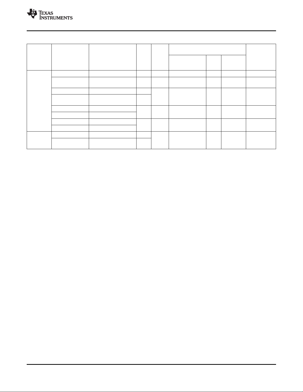
TPS65951
www.ti.com
SWCS053F –SEPTEMBER 2010–REVISED MAY 2012
Table 2-3. Signal Description (continued)
CONFIGURATION BY DEFAULT AFTER
MODULE SIGNAL NAME DESCRIPTION TYPE BALLS
LED driver VBAT.VIBRA H-Bridge Vibra VBAT Power D9 VBAT.VIBRA Power VBAT
LEDGND LED driver ground Power F10 LEDGND Power GND
GND GND
GPIO.13 GPIO.13 I/O A12 GPIO.13 I PD Floating
LEDSYNC LED synchronization I
input
LEDA LED leg A Open E9 Signal not Floating
VIBRA.P H-Bridge Vibra P
Drain Functional
LEDB LED leg B Open F11 Signal not Floating
VIBRA.M H-Bridge Vibra M
Drain Functional
Digital GPIO.16 GPIO.16 I/O C3 GPIO.16 I PD Floating
Microphone
DIG.MIC.CLK0 Digital microphone clock O
0
(1) This column provides the connection when the associated feature is not used or not connected. When there is pin multiplexing, we
consider that all functions on the multiplexed pin are not used. But even if all functions are not used, we have to consider the
configuration by default.
Special criteria: For audio features input, use capacitor to ground with a 100-nF typical value capacitor.
Not Applicable: When the associated feature is mandatory for the good working of TPS65951.
(2) Signal not functional indicates that no signal is present on the pad after a release reset.
(3) The signal VPRECH must be connected with the CPRECH capacitor to GND.
(4) VIO internal oscillator is used even if VIO output is not used; therefore, VIO has to be connected to VBAT.
RESET RELEASED
INTERNAL
SIGNAL TYPE PULL OR
NOT
(2)
(2)
NOT USED
FEATURES
(1)
Copyright © 2010–2012, Texas Instruments Incorporated Terminal Description 29
Submit Documentation Feedback
Product Folder Link(s): TPS65951
Page 30
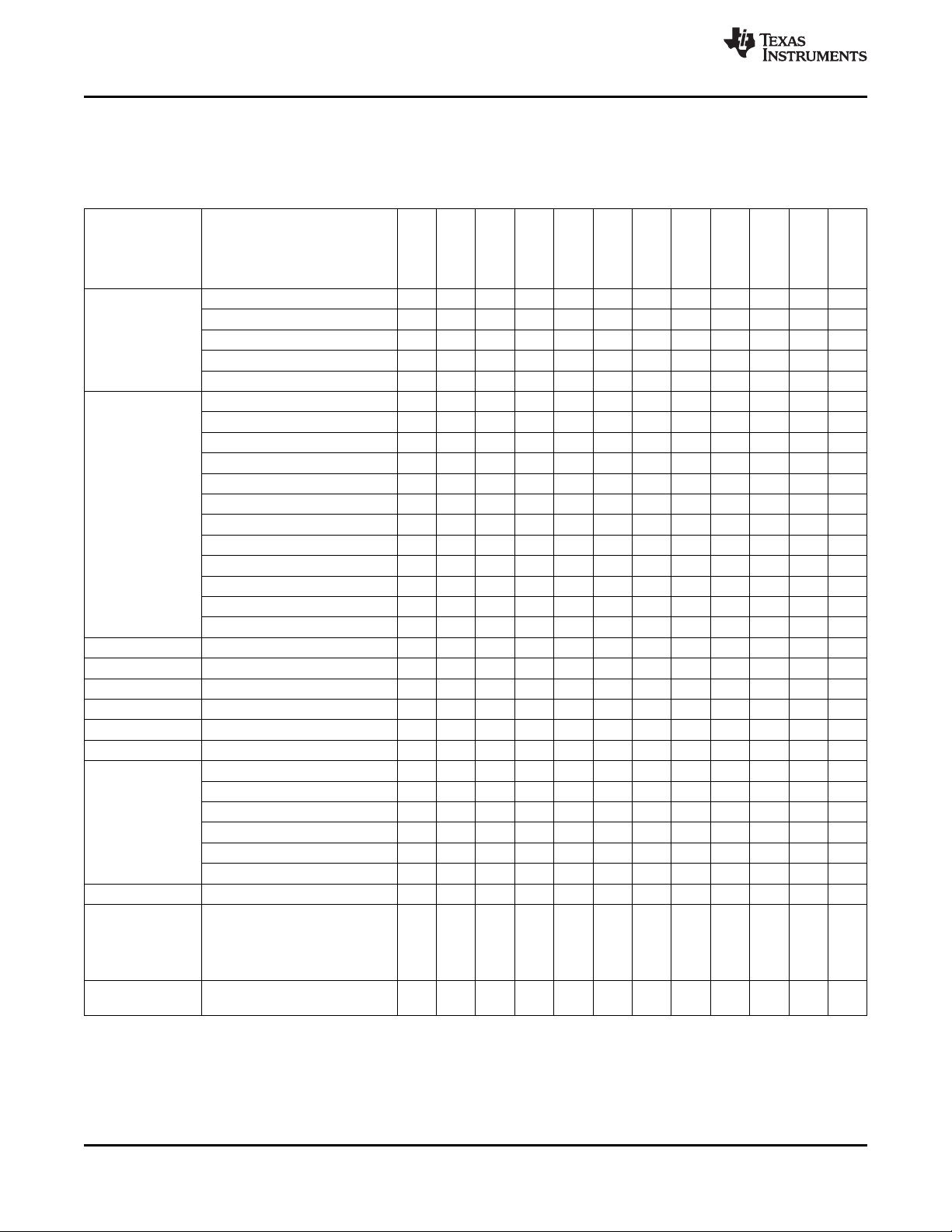
TPS65951
SWCS053F –SEPTEMBER 2010–REVISED MAY 2012
2.5 Ground Connection Usage
Ground connections for different blocks are listed in Table 2-4.
CATEGORY BLOCK
Audio Audio Uplink (TX) X
Audio Downlink (RX) X
Audio HF PLL X
Hands-Free (class-D), Left X
Hands-Free (class-D), Right X
LDO VDAC X
VPLL1 X
VPLL2 X
VMMC1 X
VMMC2 X
VAUX1 X
VAUX2 X
VAUX3 X
VAUX4 X
VINTDIG X
VINTANA1 X
VINTANA2 X
USB (including USB LDOs) X
GPADC X
BCI X
EEPROM X
BBS (Backup Battery System) X
Clock Slicer X
DC-DC VIO X
VIO Dedicated Power Ground X
VDD1 X
VDD1 Dedicated Power Ground X
VDD2 X
VDD2 Dedicated Power Ground X
Substrate Ground X
Clean, extra low current, low X
noise ground used for all
sensitive analog modules
(including band-gap voltage, 32kHz oscillator).
Digital audio filter and digital logic X
(all DGND balls are merged)
Table 2-4. Ground Connections
AVSS1
AVSS2
AVSS3
AVSS4
AGND
DGND
REFGND
VDD1.GND
VDD2.GND
www.ti.com
VIO.GND
GND.LEFT
GND.RIGHT
30 Terminal Description Copyright © 2010–2012, Texas Instruments Incorporated
Submit Documentation Feedback
Product Folder Link(s): TPS65951
Page 31

TPS65951
www.ti.com
SWCS053F –SEPTEMBER 2010–REVISED MAY 2012
3 Electrical Characteristics
3.1 Absolute Maximum Ratings
Table 3-1 lists the absolute maximum ratings.
Table 3-1. Absolute Maximum Ratings
PARAMETER TEST CONDITIONS MIN TYP MAX UNIT
Main battery supply voltage
Voltage on any input
VBUS inputs -2 20 V
Storage temperature range –55 125 °C
Ambient temperature range –40 85 °C
Junction temperature (TJ) Absolute maximum rating –40 150 °C
Junction temperature (TJ) For parametric compliance –40 125 °C
Ambient temperature for With max 125°C as Junction temperature (TJ) –40 85 °C
parametric compliance
DP, DM, ID high voltage short DP, DM, or ID pins short circuited to VBUS 5.25 V
circuit supply, in any mode of device operation,
DP, DM, ID low voltage short DP, DM, or ID pins short circuited to GND in 0 V
circuit any mode of device operation, continuously for
(1) The product will have negligible reliability impact if voltage spikes of 5.2 V occur for a total duration (cumulative over lifetime) of 10
milliseconds.
(2) Except VBAT input pads and VBUS pad.
(3) Supply equals the reference level listed in Table 2-1 for each pin.
(1)
(2)
Where supply represents the voltage applied to –0.3 1.0 × Supply + V
the power supply pin associated with the 0.3
(3)
input
continuously for 24 hours
24 hours
0 5 V
3.2 Minimum Voltages and Associated Currents
Table 3-2. VBAT Min Required Per VBAT Ball and Associated Maximum Current
Maximum Current Output Voltage (V) VBAT min (V)
Specified (mA)
VBAT pin name VPLLA3R.IN 340
Internal module VPLL1 (LDO) 40 1.0 / 1.2 / 1.3 / 1.8 maximum
supplied (2.7, output voltage selected + 250 mV)
VPLL2 (LDO) 100 0.7 / 1.0 / 1.2 / 1.3 / maximum
VAUX3 (LDO) 200 1.5 / 1.8 / 2.5 / 2.8 maximum
VDD1 core (DCDC) < 1 2.7
VDD2 core (DCDC) < 1 2.7
SYSPOR (power ref) < 1 2.7
PBIAS (power ref) < 1 2.7
VBAT pin name VDAC.IN 370
1.8 (2.7, output voltage selected + 250 mV)
(2.7, output voltage selected + 250 mV)
Copyright © 2010–2012, Texas Instruments Incorporated Electrical Characteristics 31
Submit Documentation Feedback
Product Folder Link(s): TPS65951
Page 32

TPS65951
SWCS053F –SEPTEMBER 2010–REVISED MAY 2012
www.ti.com
Table 3-2. VBAT Min Required Per VBAT Ball and Associated Maximum Current (continued)
Maximum Current Output Voltage (V) VBAT min (V)
Specified (mA)
Internal module VDAC (LDO) 70 1.2 / 1.3 / 1.8 maximum
supplied (2.7, output voltage selected + 250 mV)
VINTANA1 (LDO) 50 1.5 maximum
VINTANA2 (LDO) 250 2.5 / 2.75 maximum
VIO core (DCDC) < 1 2.7
VAUX4 core (LDO) < 1 2.7
VBAT pin name VAUX12S.IN 350
Internal module VAUX1 (LDO) 200 2.5 / 2.8 / 3.0 maximum
supplied (2.7, output voltage selected + 250 mV)
VAUX2 (LDO) 100 1.3 / 1.5 / 1.7 / 1.8 / maximum
1.9 / 2.0 / 2.1 / 2.2 / (2.7, output voltage selected + 250 mV)
2.3 / 2.4 / 2.5 / 2.8
VBAT pin name VMMC2.IN 100
VMMC2 (LDO) 100 1.85 / 2.6 / 2.85 / 3.0 maximum
/ 3.15 (2.7, output voltage selected + 250 mV)
POWER_REGBATT 0.001 2.7
VBAT pin name VMMC1.IN 220
VMMC1 (LDO) 220 1.85 / 2.85 / 3.0 / maximum
3.15 (2.7, output voltage selected + 250 mV)
POWER_REGBATT 0.001 2.7
VBAT pin name VINTDIG.IN 131
Internal module VINTDIG (LDO) 100 1.5 maximum
supplied (2.7, output voltage selected + 250 mV)
VRRTC (LDO) 30 1.5 maximum
VBRTC (LDO) 1 1.3 maximum
VBAT pin name VAUX4.IN 100
VAUX4 (LDO) 100 0.7 / 1.0 / 1.2 / 1.3 / output voltage selected + 250 mV
1.5 / 1.8 / 2.5 / 2.8
(2.7, output voltage selected + 250 mV)
(2.7, output voltage selected + 250 mV)
(2.7, output voltage selected + 250 mV)
(2.7, output voltage selected + 250 mV)
3.3 Recommended Operating Conditions
Table 3-3 lists the recommended operating maximum ratings.
Table 3-3. Recommended Operating Maximum Ratings
PARAMETER TEST CONDITIONS MIN TYP MAX UNIT
Main battery supply voltage 2.7 3.6 4.5 V
Backup battery supply voltage 1.8 3.2 3.3 V
Ambient temperature range –40 85 °C
3.4 Digital I/O Electrical Characteristics
Table 3-4 describes the digital I/O electrical characteristics.
• RL: Reference level voltage applied to the I/O cell
• VOL: Low-level output voltage
• VOH: High-level output voltage
• VIL: Low-level input voltage
• VIH: High-level input voltage
32 Electrical Characteristics Copyright © 2010–2012, Texas Instruments Incorporated
Submit Documentation Feedback
Product Folder Link(s): TPS65951
Page 33

TPS65951
www.ti.com
SWCS053F –SEPTEMBER 2010–REVISED MAY 2012
Table 3-4. Digital I/O Electrical Characteristics
VOL (V) VOH (V) VIL (V) VIH (V) MAX
Pin Name FREQ (pF)
GPIO.0/CD1
JTAG.TDO
GPIO.1/CD2
JTAG.TMS
GPIO.2
TEST1
GPIO.15
TEST2
GPIO.6
PWM0 0 0.45 RL 0 RL 3 30 5.2 5.2
TEST3
GPIO.7
VIBRA.SYNC
PWM1
TEST4
START.ADC 0.35 × 0.65 ×
SYSEN RL – 0.35 × 0.65 ×
CLKEN RL –
CLKREQ 0.35 × 0.65 ×
INT1 RL –
NRESPWRON RL –
NRESWARM 0.35 × 0.65 ×
PWRON 0.35 × 0.65 ×
NSLEEP1 0.35 × 0.65 ×
BOOT0 0 RL 3 33.3 33.3
BOOT1 0 RL 3 33.3 33.3
REGEN RL –
MSECURE 0.35 × 0.65 ×
I2C.SR.SDA 0.3 × 0.7 ×
VMODE2 0.35 × 0.65 ×
I2C.SR.SCL 0.3 × 0.7 ×
I2C.CNTL.SDA 0.3 × 0.7 ×
I2C.CNTL.SCL 0.3 × 0.7 ×
MIN MAX MIN MAX MIN MAX MIN MAX
0 0.45 RL 0 RL 33 30 5.2 5.2
0 0.45 RL 0 RL 33 30 5.2 5.2
0 0.45 RL 0 RL 3 30 5.2 5.2
0 0.45 RL 0 RL 3 30 5.2 5.2
0 0.45 RL 0 RL 3 30 5.2 5.2
0 0.45 RL 0 RL 5.2 5.2
0 0.45 RL 3 30 33.3 33.3
0 0.45 RL 3 30 33.3 33.3
0 0.45 RL 3 30 33.3 33.3
0 0.45 RL 3 30 33.3 33.3
0 0.4 –0.5 RL+0.5 3.4 up to 400
0 0.4 –0.5 RL+0.5 3.4 10 10
0 0.4 –0.5 RL+0.5 3.4 up to 400
0 0.4 –0.5 RL+0.5 3.4 10 10
RL – 0.35 × 0.65 ×
0.45 RL RL
RL – 0.35 × 0.65 ×
0.45 RL RL
RL – 0.35 × 0.65 ×
0.45 RL RL
RL – 0.35 × 0.65 ×
0.45 RL RL
RL – 0.35 × 0.65 ×
0.45 RL RL
RL – 0.35 × 0.65 ×
0.45 RL RL
0 RL 6 16.7 16.7
0.45 RL RL
0.45
0 RL 3 33.3 33.3
0.45
0.45
0 RL 3 30 33.3 33.3
0 VBAT 3 33.3 33.3
0 RL 3 33.3 33.3
0.45
0 RL 3 33.3 33.3
0 RL 3.4 29.4 29.4
RL RL
RL RL
RL RL
1.8 V 1.8 V
RL RL
RL RL
RL RL
RL RL
RL RL
RL RL
RL RL
MAX LOAD
(MHz) OUTPUT
MODE
MAX MAX
(1)
RISE
TIME TIME
FALL
(ns) (ns)
(1)
Copyright © 2010–2012, Texas Instruments Incorporated Electrical Characteristics 33
Submit Documentation Feedback
Product Folder Link(s): TPS65951
Page 34

TPS65951
SWCS053F –SEPTEMBER 2010–REVISED MAY 2012
www.ti.com
Table 3-4. Digital I/O Electrical Characteristics (continued)
VOL (V) VOH (V) VIL (V) VIH (V) MAX
MAX LOAD
Pin Name FREQ (pF)
MIN MAX MIN MAX MIN MAX MIN MAX
(MHz) OUTPUT
MODE
PCM.VCK RL – 0.35 × 0.65 ×
PCM.VDR RL – 0.35 × 0.65 ×
PCM.VDX RL – 0.35 × 0.65 ×
PCM.VFS RL – 0.35 × 0.65 ×
I2S.CLK RL – 0.35 × 0.65 ×
I2S.SYNC RL – 0.35 × 0.65 ×
I2S.DIN 0.35 × 0.65 ×
I2S.DOUT RL –
DIG.MIC.0 0.35 × 0.65 ×
RTSO/
CLD64K.OUT/ 0 0.45 RL 3 30 33 33
BERCLK.OUT
CTSI/ RL – 0.35 × 0.65 ×
BERDATA.OUT 0.45 RL RL
MANU_BRIX RL –
USBCHRG_ENZ RL –
USBCHRG_STAT 0.35 × 0.65 ×
Z RL RL
CHRG_DET_N RL –
32KCLKOUT RL –
HFCLKOUT RL –
UCLK RL – 0.35 × 0.65 ×
STP
GPIO.9
DIR
GPIO.10
NXT
GPIO.11
DATA0
UART4.TXD
DATA1
UART4.RXD
DATA2
UART4.RTSI
DATA3
UART4.CTSO
0 0.45 RL 0 RL 1 30 100 33
0 0.45 RL 0 RL 1 30 100 100
0 0.45 RL 0 RL 1 30 100 33
0 0.45 RL 0 RL 1 30 33 33
0 0.45 RL 0 RL 6.5 30 33 33
0 0.45 RL 0 RL 6.5 30 33 33
0 0.45 RL 3.25 30 29 29
0.45 RL RL
0.45 RL RL
0.45 RL RL
0.45 RL RL
0.45 RL RL
0.45 RL RL
0 RL 3.25 30 33 33
RL RL
0.45
0 RL 2.4 41.7 41.7
RL RL
RL –
0.45
0 0.45 RL 0 RL 3 30 33 33
0 0.45 RL 3 30 33 33
0 0.3 RL 3 30 33 33
0.45
0.1
0 RL 3 33 33
0 0.3 RL 3 30 33 33
0 0.45 RL 0.032 40 16 16
0 0.45 RL 38.4 30 5.0
0 0.45 RL 0 RL 60 10 1 1
0 0.45 RL 0 RL 30 10 1 1
0 0.45 RL 0 RL 30 10 1 1
0 0.45 RL 0 RL 30 10 1 1
0 0.45 RL 0 RL 30 10 1 1
0 0.45 RL 0 RL 30 10 1 1
0 0.45 RL 0 RL 30 10 1 1
0 0.45 RL 0 RL 30 10 1 1
0.1
0.45
0.45
0.45 RL RL
RL – 0.35 × 0.65 ×
0.45 RL RL
RL – 0.35 × 0.65 ×
0.45 RL RL
RL – 0.35 × 0.65 ×
0.45 RL RL
RL – 0.35 × 0.65 ×
0.45 RL RL
RL – 0.35 × 0.65 ×
0.45 RL RL
RL – 0.35 × 0.65 ×
0.45 RL RL
RL – 0.35 × 0.65 ×
0.45 RL RL
MAX MAX
(1)
RISE
FALL
TIME TIME
(ns) (ns)
(2)
4.7
(1)
(2)
34 Electrical Characteristics Copyright © 2010–2012, Texas Instruments Incorporated
Submit Documentation Feedback
Product Folder Link(s): TPS65951
Page 35

TPS65951
www.ti.com
SWCS053F –SEPTEMBER 2010–REVISED MAY 2012
Table 3-4. Digital I/O Electrical Characteristics (continued)
VOL (V) VOH (V) VIL (V) VIH (V) MAX
Pin Name FREQ (pF)
GPIO.12 RL – 0.35 × 0.65 ×
DATA4
GPIO.14
DATA5
GPIO.3
DATA6
GPIO.4
DATA7
GPIO.5
TEST.RESET 0.35 × 0.65 ×
TEST 0.35 × 0.65 ×
JTAG.TDI/ 0.35 × 0.65 ×
BERDATA RL RL
JTAG.TCK/ 0.35 × 0.65 ×
BERDATA RL RL
GPIO.13
LEDSYNC
GPIO.16 RL – 0.35 × 0.65 ×
DIG.MIC.CLK0 RL –
(1) Min value depends on board conditions, and can be computed with IBIS-models.
(2) Max rise/fall times valid for high drive settings and max load of 20 pF.
MIN MAX MIN MAX MIN MAX MIN MAX
0 0.45 RL 0 RL 30 10 1 1
0 0.45 RL 0 RL 30 10 1 1
0 0.45 RL 0 RL 30 10 1 1
0 0.45 RL 0 RL 30 10 1 1
0 0.45 RL 0 RL 30 10 1 1
0 0.45 RL 0 RL 3 30 33.3 33.3
0 0.45 RL 0 RL 3 30 33.3 33.3
0 0.45 RL 2.4 30 41.7 41.7
0.45 RL RL
RL – 0.35 × 0.65 ×
0.45 RL RL
RL – 0.35 × 0.65 ×
0.45 RL RL
RL – 0.35 × 0.65 ×
0.45 RL RL
RL – 0.35 × 0.65 ×
0.45 RL RL
0 RL 3 33 33
0 RL 3 30 29 29
0 RL 3 33 33
0 RL 3 33 33
RL – 0.35 × 0.65 ×
0.45 RL RL
0.45 RL RL
0.45
RL RL
RL RL
MAX LOAD
(MHz) OUTPUT
MODE
MAX MAX
(1)
RISE
TIME TIME
FALL
(ns) (ns)
(1)
Copyright © 2010–2012, Texas Instruments Incorporated Electrical Characteristics 35
Submit Documentation Feedback
Product Folder Link(s): TPS65951
Page 36

Device
32KXOUT
OR
HFCLKIN
32KCLKOUT
HFCLKOUT
32KXIN
OR
OR
32 kHz
SWCS053-004
TPS65951
SWCS053F –SEPTEMBER 2010–REVISED MAY 2012
4 Clock Specifications
The TPS65951 includes several I/O clock pins. The TPS65951 has two sources of high-stability clock
signals: the external high-frequency clock (HFCLKIN) input and an on-board 32-kHz oscillator (optionally,
an external 32-kHz signal can be provided). Figure 4-1 shows the clock overview.
www.ti.com
4.1 Features
The TPS65951 accepts two sources of high-stability clock signals:
• 32KXIN/32KXOUT: on-board 32-kHz crystal oscillator (optionally, an external 32-kHz input clock can
be provided)
• HFCLKIN: an external high-frequency clock (19.2, 26, or 38.4 MHz)
The TPS65951 has the capability to provide:
• 32KCLKOUT digital output clock
• HFCLKOUT digital output clock with the same frequency as HFCLKIN input clock
4.2 Clock Slicer
Figure 4-2 show the clock slicer block diagram.
Figure 4-1. Clock Overview
36 Clock Specifications Copyright © 2010–2012, Texas Instruments Incorporated
Submit Documentation Feedback
Product Folder Link(s): TPS65951
Page 37

PL_HR resistance
CDM
clamp
HFCLKIN
HFCLKOUT
PWRDN, PWRSEL
BYPASS, PWRDN, PWRSEL
Cc
OR
SWCS053-005
TPS65951
www.ti.com
The clock slicer is disabled by default and enabled when the CLKEN PAD is high. The slicer transforms
the HFCLKIN clock input signal into a squared clock signal used internally by the TPS65951 and also
outputs it for external use. The HFCLKIN input signal can be:
• A sinusoid with peak-to-peak amplitude varying from 0.3 to 1.45 V
• A square-wave clock signal with maximum amplitude of 1.85 V. In the case of a square-wave clock
SWCS053F –SEPTEMBER 2010–REVISED MAY 2012
Figure 4-2. Clock Slicer Block Diagram
signal, the slicer will be configured in bypass or power-down mode (see Section 4.2.1).
The HFCLKIN input clock frequency must be 19.2, 26, or 38.4 MHz.
4.2.1 Modes of Operation
There are four different modes programmable by register. By default, the slicer is in a high-performance
application mode.
4.2.1.1 Bypass Mode (BP)
In BP mode which overrides all the other modes, the input signal is directly connected to the output
through some buffers. The input is a rail-to-rail square wave.
4.2.1.2 Power-Down Mode (PD)
During PD mode if bypass mode is not active, the cell does not consume any current if bypass mode is
not active.
4.2.1.3 Low-Power Application Mode (LP)
In LP mode, the input sine wave is converted to a CMOS signal (square wave) with low-power
consumption.
4.2.1.4 High-Performance Application Mode (HP)
In HP mode, the input sine wave is converted to a CMOS signal (square wave). It has lower duty cycle
degradation and input-to-output delay in comparison to the low-power mode, but it consumes more
current. The drive of the squaring inverter is increased by connecting additional inverters in parallel.
Details can be found in the clock slicer electrical characteristics table (see Table 4-1).
Copyright © 2010–2012, Texas Instruments Incorporated Clock Specifications 37
Submit Documentation Feedback
Product Folder Link(s): TPS65951
Page 38

TPS65951
SWCS053F –SEPTEMBER 2010–REVISED MAY 2012
www.ti.com
4.2.2 Clock Slicer Electrical Characteristics
Table 4-1 summarizes the clock slicer electrical characteristics.
Table 4-1. Clock Slicer Electrical Characteristics
PARAMETER MODE MIN TYP MAX UNIT
Input frequency 10 26 40 MHz
Input dynamic range V
Harmonic content of input signal (with 0.7-VPPamplitude): 2nd component LP / HP –25 dBc
Input clock signal duty cycle 40% 60%
Internal coupling capacitor 4.2 5 5.7 pF
Parallel input resistance over 10 to 40 MHz range HP 30 75 kΩ
Parallel input capacitance over 10 MHz to 40 MHz range HP 0.3 0.7 pF
Output duty cycle with VIN= 0.2 V
Propagation delay HP 3 15 ns
Power supply rejection ratio sideband (1% RMS of supply voltage added sine 5 MHz) LP / HP 26 dBc
Current consumption at maximum input of 40 MHz HP 235 μA
Power-up time LP / HP 1 ms
Output peak-to-peak jitter with an input peak-to-peak jitter < 0.1% and for jitter frequency LP / HP 0.2%
below 300 kHz
Output peak-to-peak jitter with an input peak-to-peak jitter < 0.1% and for jitter frequency LP / HP 1%
above 300 kHz
(1) Bypass input maximum voltage is the same as the maximum voltage provided for the I/O interface.
PP
LP / HP 0.3 0.7 1.45
BP / PD 0 1.85
LP 15 60 kΩ
BP / PD 1 100 MΩ
LP 0.3 0.8
BP / PD 0.08 1
LP / HP 40% 50% 60%
LP 4 18
BP / PD 0.2 3
LP 175 μA
BP / PD 39 nA
(1)
PP
38 Clock Specifications Copyright © 2010–2012, Texas Instruments Incorporated
Submit Documentation Feedback
Product Folder Link(s): TPS65951
Page 39

HFCLKIN
SLEEP1
CLKEN
Clock
generator
CLKREQ
Main state-machine
Optional request
configurable by software
only for legacy support
HFCLKOUT
Slicer
SLICER_OK
Slicer bypass
SWCS053-006
TPS65951
www.ti.com
4.3 Input Clock Specifications
The clock system accepts two input clock sources:
• 32-kHz crystal oscillator clock or sinusoidal/squared clock
• HFCLKIN high frequency input clock
4.3.1 Clock Source Requirements
Table 4-2 summarizes the input clock requirements.
Table 4-2. TPS65951 Input Clock Source Requirements
PAD CLOCK FREQUENCY STABILITY DUTY CYCLE
32KXIN
32KXOUT
HFCLKIN 19.2 MHz, 26 MHz, 38.4 MHz
32.768 kHz Square wave – 45% / 55%
4.3.2 High Frequency Input Clock
HFCLKIN stands for high frequency input clock. It can be either a square- or a sine-wave input clock. If a
square-wave input clock is provided, it is recommended to switch the block to bypass mode when possible
to avoid loading the clock (see Section 4.2).
SWCS053F –SEPTEMBER 2010–REVISED MAY 2012
Crystal ±30 ppm 40% / 60%
Sine wave – –
Square wave ±150 PPM 45% / 55%
Sine wave – –
Figure 4-3 shows the HFCLKIN clock distribution.
Figure 4-3. HFCLKIN Clock Distribution
Copyright © 2010–2012, Texas Instruments Incorporated Clock Specifications 39
Submit Documentation Feedback
Product Folder Link(s): TPS65951
Page 40

VIO
PERIPH1
Device
VIO
PERIPH2
VIO
PERIPHn
CLKREQ
SWCS053-007
TPS65951
SWCS053F –SEPTEMBER 2010–REVISED MAY 2012
When a device needs a clock signal other than 32.768 kHz, it makes a clock request and activates the
CLKREQ pin. As a result, the TPS65951 immediately sets CLKEN to 1 to warn the clock provider in the
system about the clock request. Then, the TPS65951 opens a gated clock and a high-frequency output
clock signal is available through the HFCLKOUT pin. The output drive of HFCLKOUT is programmable
(low drive (MISC_CFG[CLK_HF_DRV] = 0) max load 20 pF, high drive (MISC_CFG[CLK_HF_DRV] = 1)
maximum load 30 pF), by default it is programmed to support low drive.
CLKREQ has a weak pulldown resistor to support the wired-OR clock request.
Figure 4-4 shows an example of the wired-OR clock request.
www.ti.com
Figure 4-4. Example of Wired-OR Clock Request
Note that the timer default value must be the worst case (10 ms) for the clock providers. For legacy or
workaround support, the signal NSLEEP1 can also be used as a clock request even if it is not its primary
goal. By default, this feature is disabled and must be enabled individually by setting the register bits
associated with each signal.
Table 4-3 details the input clock electrical characteristics of the HFCLKIN input clock.
40 Clock Specifications Copyright © 2010–2012, Texas Instruments Incorporated
Submit Documentation Feedback
Product Folder Link(s): TPS65951
Page 41

HFCLKIN
CH0 CH1
CH0–CH1
SWCS053-088
TPS65951
www.ti.com
SWCS053F –SEPTEMBER 2010–REVISED MAY 2012
Table 4-3. HFCLKIN Input Clock Electrical Characteristics
PARAMETER DESCRIPTION CONFIGURATION MODE UNIT
Frequency 19.2, 26, or 38.4 MHz
Start-up time LP / HP (sine wave) 4 μs
Input dynamic range V
Current consumption HP 235
Harmonic content of input signal (with 0.7-VPPamplitude): LP / HP (sine wave) –25 dBc
2nd component
VIHVoltage input high
VILVoltage input low
(1) Bypass input max voltage is the same as the maximum voltage provided for the I/O interface (IO.1P8V).
(1)
(1)
LP / HP (sine wave) 0.3 0.7 1.45
BP / PD (square wave) 0 1.85
LP 175
BP / PD 39 nA
BP (square wave) 0.65 × V
BP (square wave) 0.35 × V
SLICER
MIN TYP MAX
IO.1P8
Table 4-4 details the input clock timing requirements of the HFCLKIN input clock when the source is a
square wave.
Table 4-4. HFCLKIN Square Input Clock Timing Requirements with Slicer in Bypass
IO.1P8
PP
(1)
μA
NAME PARAMETER DESCRIPTION MIN TYP MAX UNIT
CH0 1/t
CH1 t
CH3 t
CH4 t
C(HFCLKIN)
W(HFCLKIN)
R(HFCLKIN)
F(HFCLKIN)
Frequency, HFCLKIN 19.2, 26, or 38.4 MHz
Pulse duration, HFCLKIN low or high 0.45 × t
Rise time, HFCLKIN 0 5 ns
Fall time, HFCLKIN 0 5 ns
C(HFCLKIN)
0.55 × t
C(HFCLKIN)
Figure 4-5. HFCLKIN Squared Input Clock
4.3.3 32-kHz Input Clock
A 32.768-kHz input clock (often abbreviated to 32-kHz) generates the clocks for the RTC. It has a low-jitter
mode where the current consumption increases for lower jitter. It is possible to use the 32-kHz input clock
with either an external crystal or clock source. Depending on the mode chosen, the 32K oscillator is
configured as being either:
• An external 32.768-kHz crystal through the 32KXIN/32KXOUT balls (see Figure 4-6). This
configuration is available for the master mode only (for more details, see Section 7).
• An external square/sine wave of 32.768 kHz through 32KXIN with amplitude equal to 1.8 or 1.85 V
(see Figure 4-8, Figure 4-9). This configuration is available for the master and slave modes (for more
details, see Section 7).
ns
4.3.3.1 External Crystal Description
Figure 4-6 shows the 32-kHz oscillator block diagram with crystal in master mode.
Copyright © 2010–2012, Texas Instruments Incorporated Clock Specifications 41
Submit Documentation Feedback
Product Folder Link(s): TPS65951
Page 42

Signal swing
limiting circuit
Bias generator
and startup
circuit
XI
XO
Signal
shaping
CXIN
CXOUT
Y
Current control
circuit and
mode selection
XTAL
External to device
VBATOK
(1)
Internal
GND
Internal
GND
VBATOK
(1)
SWCS053-091
TPS65951
SWCS053F –SEPTEMBER 2010–REVISED MAY 2012
www.ti.com
NOTE: Switches close by default and open only if register access enables the very-low-power mode when VBAT < 2.7 V.
Figure 4-6. 32-kHz Oscillator Block Diagram In Master Mode With Crystal
CXIN and CXOUT represent the total capacitance of the PCB and components, excluding the crystal.
Their values depend on the datasheet of the crystal, also the internal capacitors and the parallel capacitor.
The frequency of the oscillations depends on the value of the capacitors. The crystal must be in the
fundamental mode of operation and parallel resonant.
NOTE
For the values of CXIN and CXOUT, see Table 12-1, TPS65951 External Components.
Table 4-5 summarizes the required electrical constraints.
Table 4-5. Crystal Electrical Characteristics
PARAMETER MIN TYP MAX UNIT
Parallel resonance crystal frequency 32.768 kHz
Input voltage, Vin (normal mode) 1.0 1.3 1.55 V
Internal capacitor on each input (Cint) 8 10 12 pF
Parallel input capacitance (Cpin) 1 pF
Nominal load cap on each oscillator input CXIN and CXOUT
Pin to pin capacitance 1.6 1.8 pF
(1)
CXIN = CXOUT = Cosc × 2 – (Cint pF
+ Cpin)
(1) Nominal load capacitor on each oscillator input defined as CXIN = CXOUT = Cosc × 2 – (Cint + Cpin). Cosc is the load capacitor
42 Clock Specifications Copyright © 2010–2012, Texas Instruments Incorporated
defined in the crystal oscillator specification, Cint is the internal capacitor, and Cpin is the parallel input capacitor.
Submit Documentation Feedback
Product Folder Link(s): TPS65951
Page 43

C
C
O
L
ESR R= 1 +
m
2
SWCS053-e001
32KX
OC0
OC0–OC1
OC1
SWCS053-009
TPS65951
www.ti.com
SWCS053F –SEPTEMBER 2010–REVISED MAY 2012
Table 4-5. Crystal Electrical Characteristics (continued)
PARAMETER MIN TYP MAX UNIT
Crystal ESR
Crystal shunt capacitance, C
Crystal tolerance at room temperature, 25°C –30 30 ppm
Crystal tolerance versus temperature range (–40°C to 85°C) –200 200 ppm
Maximum drive power 1 μW
Operating drive level 0.5 μW
Crystal quality factor 13k 54k
(2) The crystal motional resistance Rm relates to the equivalent series resistance (ESR) by the following formula:
(2)
O
Measured with the load capacitance specified by the crystal manufacturer. In fact, if CXIN = CXOUT = 10 pF, then CL= 5 pF. Parasitic
capacitance from the package and board must also be taken in account.
90 kΩ
1 pF
When selecting a crystal, the system designer must consider the temperature and aging characteristics of
a crystal versus the user environment and expected lifetime of the system.
Table 4-6 and Table 4-7 list the switching characteristics of the oscillator and the input requirements of the
32.768-kHz input clock. Figure 4-7 shows the crystal oscillator output in normal mode.
Table 4-6. Base Oscillator Switching Characteristics
NAME PARAMETER DESCRIPTION MIN TYP MAX UNIT
f
P
t
SX
I
DDA
I
DDQ
Oscillation frequency 32.768 kHz
Start-up time, all conditions 500 ms
Start-up tine, 25°C 360
Active current consumption High jitter mode 1.8
(configured through LOJIT register μA
bit)
Current consumption μA
Low jitter mode 8
Low battery mode (1.2 V) 1
Startup 8
Table 4-7. 32-kHz Crystal Input Clock Timing Requirements
NAME PARAMETER DESCRIPTION MIN TYP MAX UNIT
OC0 1/t
OC1 t
C(32KHZ)
W(32KHZ)
Frequency, 32 kHz 32.768 kHz
Pulse duration, 32 kHz low or high 0.40 × t
C(32KHZ)
0.60 × t
C(32KHZ)
Figure 4-7. 32-kHz Crystal Input
4.3.3.2 External Clock Description
Figure 4-8 shows the 32-kHz oscillator block diagram with a 32.768-kHz square- or sine-wave signal in
master and slave modes. Figure 4-9 shows an external clock source when the oscillator is configured in
bypass mode. Thus, there are two configurations:
• A square- or sine-wave input can be applied to the 32KXIN pin with amplitude of 1.85 or 1.8 V. The
32KXOUT pin can be left floating. This configuration, showed in Figure 4-8, is used if no charge is
applied on the 32KXOUT pin.
μs
Copyright © 2010–2012, Texas Instruments Incorporated Clock Specifications 43
Submit Documentation Feedback
Product Folder Link(s): TPS65951
Page 44

Signal swing
limiting circuit
Bias generator
and startup
circuit
XI XO
Signal
shaping
Square/sine wave:
Vpp = VBRTC or
VIO_1P8V
Y
Current control
circuit and mode
selection
Floating
VBATOK
(1)
Internal
GND
Internal
GND
VBATOK
(1)
SWCS053-010
TPS65951
SWCS053F –SEPTEMBER 2010–REVISED MAY 2012
• The oscillator is in bypass mode and a square-wave input can be applied to the 32KXIN pin with
amplitude of 1.8 V. The 32KXOUT pin can be left floating. This configuration, shown in Figure 4-9, is
used if the oscillator is in bypass mode.
www.ti.com
(1) Switches close by default and open only if register access enables the very-low-power mode when VBAT < 2.7 V.
Figure 4-8. 32-kHz Oscillator Block Diagram Without Crystal Option 1
44 Clock Specifications Copyright © 2010–2012, Texas Instruments Incorporated
Submit Documentation Feedback
Product Folder Link(s): TPS65951
Page 45

Signal swing
limiting circuit
Bias generator
and startup
circuit
XI
XO
Signal
shaping
Square wave:
Vpp = VIO_1P8V
Y
Current control
circuit and mode
selection
Floating
VBATOK
(1)
Internal
GND
Internal
GND
VBATOK
(1)
SWCS053-011
TPS65951
www.ti.com
SWCS053F –SEPTEMBER 2010–REVISED MAY 2012
(1) Switches close by default and open only if register access enables the very-low-power mode when VBAT < 2.7 V.
Figure 4-9. 32-kHz Oscillator in Bypass Mode Block Diagram Without Crystal Option 2
Table 4-8 summarizes the electrical constraints required by the 32-kHz input square- or sine-wave clock
used:
Table 4-8. 32-kHz Input Square- or Sine-wave Clock Source Electrical Characteristics
NAME PARAMETER DESCRIPTION MIN TYP MAX UNIT
f Frequency 32.768 kHz
C
I
C
FI
V
PP
V
IH
V
IL
Input capacitance 28 35 42 pF
On-chip foot capacitance to GND on each input (see Figure 4-8, Figure 4-9) 8 10 12 pF
Square-/sine-wave amplitude in bypass mode or not 1.5
Voltage input high, square wave in bypass mode
Voltage input low, square wave in bypass mode
(1)
0.65 × V
VBRTC
(2)
(1)
0.35 × V
VBRTC
V
(1) Bypass input max voltage is the same as the maximum voltage provided for the I/O interface. The input buffer is supplied by VBRTC,
but it is supported up to IO.1P8. Because the input buffer is supplied VBRTC, VIH and VIL are relative to VBRTC.
(2) Bypass input max voltage is the same as the maximum voltage provided for the I/O interface. The input buffer is supplied by VBRTC,
but it is supported up to IO.1P8. Because the input buffer is supplied VBRTC, VIH and VIL are relative to VBRTC.
Table 4-9 details the input requirements of the 32-kHz square-wave input clock.
Table 4-9. 32-kHz Square-wave Input Clock Source Timing Requirements
C(32KHZ)
0.55 × t
0.1 × t
0.1 × t
C(32KHZ)
C(32KHZ)
C(32KHZ)
μs
μs
μs
NAME PARAMETER DESCRIPTION MIN TYP MAX UNIT
CK0 1/t
CK1 t
CK3 t
CK4 t
(1) The capacitive load is equivalent to 30 pF.
W(32KHZ)
R(32KHZ)
F(32KHZ)
C(32KHZ)
Frequency, 32 kHz 32.768 kHz
Pulse duration, 32 kHz low or high 0.45 × t
Rise time, 32 kHz
Fall time, 32 kHz
(1)
(1)
Copyright © 2010–2012, Texas Instruments Incorporated Clock Specifications 45
Submit Documentation Feedback
Product Folder Link(s): TPS65951
Page 46

32KX
CK0
CK0–CK1
CK1
SWCS053-087
OR
OR
32 kHz
32KXIN
32KXOUT
32-kHz
OSC
IO_1P8
(1.8 V)
32KCLKOUT
RTC
SWCS053-012
TPS65951
SWCS053F –SEPTEMBER 2010–REVISED MAY 2012
Figure 4-10. 32-kHz Square- or Sine-Wave Input Clock
4.4 Output Clock Specifications
The TPS65951 device provides two output clocks:
• 32KCLKOUT
• HFCLKOUT
4.4.1 32KCLKOUT Output Clock
Figure 4-11 shows the block diagram for the 32.768-kHz clock output.
www.ti.com
Figure 4-11. 32.768-kHz Clock Output Block Diagram
The TPS65951 device has an internal 32.768-kHz oscillator connected to either an external 32.768-kHz
crystal through the 32KXIN/32KXOUT balls or an external digital 32.768-kHz clock through the 32KXIN
input (see Figure 4-11). The TPS65951 device also generates a 32.768-kHz digital clock through the
32KCLKOUT pin and can broadcast it externally to the application processor or any other devices. The
32KCLKOUT clock is broadcast by default in the TPS65951 ACTIVE state.
The 32.768-kHz clock (or signal) is also used to clock the RTC (real-time clock) embedded in the
TPS65951. The RTC is not enabled by default. It is up to the host processor to set the correct date and
time and to enable the RTC functionality.
The 32KCLKOUT output buffer can drive several devices (up to 40-pF load). At start-up, the 32.768-kHz
output clock (32KCLKOUT) must be stabilized (frequency/duty cycle) prior to the signal output (description
in TRM 3.3.2.2 32-kHz Oscillator Stabilization).
Table 4-10 summarizes the output clock electrical characteristics.
46 Clock Specifications Copyright © 2010–2012, Texas Instruments Incorporated
Submit Documentation Feedback
Product Folder Link(s): TPS65951
Page 47

32KCLKOUT
CK0 CK1 CK0-CK1
SWCS038-037
TPS65951
www.ti.com
SWCS053F –SEPTEMBER 2010–REVISED MAY 2012
Table 4-10. 32KCLKOUT Output Clock Electrical Characteristics
NAME PARAMETER DESCRIPTION MIN TYP MAX UNIT
f Frequency 32.768 kHz
C
L
V
OUT
V
OH
V
OL
Load capacitance 40 pF
Output clock voltage, depending on output reference level IO.1P8 (see Section 2) 1.8
Voltage output high V
– 0.45 V
OUT
(1)
OUT
Voltage output low 0 0.45 V
(1) The output voltage depends on output reference level which is IO.1P8 (see Section 2, Terminal Description).
Table 4-11 details the output clock timing characteristics. Figure 4-12 shows the 32KCLKOUT output clock
waveform.
Table 4-11. 32KCLKOUT Output Clock Switching Characteristics
NAME PARAMETER DESCRIPTION MIN TYP MAX UNIT
CK0 1/t
CK1 t
CK2 t
CK3 t
C(32KCLKOUT)
W(32KCLKOUT)
R(32KCLKOUT)
F(32KCLKOUT)
SSB Phase At 1-kHz offset from the carrier –110 dBc/Hz
Noise
(1) The output capacitive load is equivalent to 30 pF.
Frequency 32.768 kHz
Pulse duration, 32KCLKOUT low or high 0.40 × 0.60 × ns
Rise time, 32KCLKOUT
Fall time, 32KCLKOUT
t
(1)
(1)
C(32KCLKOUT)
4 16 ns
4 16 ns
t
C(32KCLKOUT)
V
V
Figure 4-12. 32KCLKOUT Output Clock
4.4.2 HFCLKOUT Output Clock
Table 4-12 summarizes the HFCLKOUT output clock electrical characteristics (for more information, see
Section 4.2).
Table 4-12. HFCLKOUT Output Clock Electrical Characteristics
NAME PARAMETER DESCRIPTION MIN TYP MAX UNIT
f Frequency 19.2, 26, or 38.4 MHz
C
L
V
OUT
V
OH
V
OL
(1) The output voltage depends on output reference level which is IO.1P8 (see Section 2).
NAME PARAMETER DESCRIPTION MIN TYP MAX UNIT
CHO1 1/t
CHO2 t
Load capacitance 30 pF
Output clock voltage, depending on output reference level IO.1P8 (see Section 2) 1.8
Voltage output high V
– 0.45 V
OUT
(1)
OUT
Voltage output low 0 0.45 V
Table 4-13 details the HFCLKOUT output clock timing characteristics.
Table 4-13. HFCLKOUT Output Clock Switching Characteristics
C(HFCLKOUT)
W(HFCLKOUT)
Frequency 19.2, 26, or 38.4 MHz
Pulse duration, HFCLKOUT low or high 0.40 × t
C(HFCLKOUT)
0.60 × t
C(HFCLKOUT)
V
V
ns
Copyright © 2010–2012, Texas Instruments Incorporated Clock Specifications 47
Submit Documentation Feedback
Product Folder Link(s): TPS65951
Page 48

HFCLKOUT
CHO1 CHO2
CHO1–CHO2
SWCS053-014
Tstartup
Delay1
Delay2
XIN
Starting_Event
CLK32KOUTEN
CLK32KOUT
CLKEN
HFCLKOUTEN
HFCLKOUT
NRESPWRON
SWCS053-015
TPS65951
SWCS053F –SEPTEMBER 2010–REVISED MAY 2012
www.ti.com
Table 4-13. HFCLKOUT Output Clock Switching Characteristics (continued)
NAME PARAMETER DESCRIPTION MIN TYP MAX UNIT
Rise time, HFCLKOUT, Low Drive
Load: 5 pF 0.5 3.8
CHO3 t
CHO4 t
(1) Low Drive: MISC_CFG[CLK_HF_DRV] = 0 (default)
(2) High Drive: MISC_CFG[CLK_HF_DRV] = 1
R(HFCLKOUT)
F(HFCLKOUT)
Load: 10 pF 1 5.5
Rise time, HFCLKOUT, High Drive
Load: 10 pF 0.5 2.9
Load: 20 pF 1 5.0
Fall time, HFCLKOUT, Low Drive
Load: 5 pF 0.5 3.5
Load: 10 pF 1 5.1
Rise time, HFCLKOUT, High Drive
Load: 10 pF 0.5 2.7
Load: 20 pF 1 4.7
(1)
(2)
(1)
(2)
Figure 4-13 shows the HFCLKOUT output clock waveform and Figure 4-15 shows the HFCLKOUT
behavior.
ns
ns
Figure 4-13. HFCLKOUT Output Clock
4.4.3 Output Clock Stabilization Time
Figure 4-14 shows the 32KCLKOUT and HFCLKOUT clock stabilization time.
NOTE: Tstartup, Delay1, Delay2, Delay3 depend on the boot mode (see Section 6.5, Power Management)
Figure 4-14. 32KCLKOUT and HFCLKOUT Clock Stabilization Time
In Figure 4-15, HFCLKIN is the input signal of the clock slicer coming from an external source.
HFCLKOUT is the output of the clock slicer; a squared clock signal that is present after the propagation
delay of the clock slicer (for numerical values, see Table 4-1).
48 Clock Specifications Copyright © 2010–2012, Texas Instruments Incorporated
Submit Documentation Feedback
Product Folder Link(s): TPS65951
Page 49

HFCLKIN
HFCLKOUT
SWCS053-016
TPS65951
www.ti.com
SWCS053F –SEPTEMBER 2010–REVISED MAY 2012
Figure 4-15. HFCLKOUT Behavior
Copyright © 2010–2012, Texas Instruments Incorporated Clock Specifications 49
Submit Documentation Feedback
Product Folder Link(s): TPS65951
Page 50

Stereo headset
Stereo
hands-free
class D
Mono ear piece
Main
microphone
Submicrophone
Headset
microphone
Stereo auxiliary
input
Digital
microphone
Voice
PCM
interface
Audio
TDM/I2S
interface
High-speed
I C
2
(control)
Audio/Voice Module
HFCLKIN
Bias LDOs
(x3)
Predriver
Vibrator
H-bridge
Device
SWCS053-017
Predrivers
TPS65951
SWCS053F –SEPTEMBER 2010–REVISED MAY 2012
5 Audio/Voice Module
Figure 5-1 shows the audio/voice module block diagram.
www.ti.com
Figure 5-1. Audio/Voice Module Block Diagram
5.1 Audio/Voice Downlink (RX) Module
The audio/voice module includes the following output stages:
• Mono/stereo single-ended headset amplifier
• Stereo differential integrated class D 8-Ω hands-free amplifiers
• Predrivers output signals for external class D amplifiers (single-ended)
• Mono differential earpiece amplifier
• Vibrator H-bridge
50 Audio/Voice Module Copyright © 2010–2012, Texas Instruments Incorporated
Product Folder Link(s): TPS65951
Submit Documentation Feedback
Page 51

Digital PGA
gain = 0 dB
Analog PGA
gain = 2 dB
Amp
6 dB
DAC
4.0 Vpp diff
0dBFs
SWCS053-018
TPS65951
www.ti.com
SWCS053F –SEPTEMBER 2010–REVISED MAY 2012
All output stages of the downlink (except Class-D of the Hands-Free) are powered by VINTANA2.
Characteristics are given for a VBAT higher than 3.0 V (involving VINTANA2 output level equal 2.75 V).
When VBAT is in the range of 2.7 to 3.0 V (VINTANA2 = 2.5 V), only functionality is ensured.
5.1.1 Earphone Output
5.1.1.1 Earphone Output Characteristics
Analog signals from the audio and/or voice interface are fed to the earphone amplifier. This amplifier with
different gains provides a full differential signal on terminals EARP and EARM. Figure 5-2 shows the
earphone amplifier. Table 5-1 summarizes the earphone output characteristics.
Figure 5-2. Earphone Amplifier
Table 5-1. Earphone Amplifier Output Characteristics
PARAMETER TEST CONDITIONS MIN TYP MAX UNIT
Differential load impedance 26 32 Ω
0 100 pF
Gain range
Absolute gain error –1 1 dB
Gain variation with frequency F = 20 Hz to 20 kHz –0.5 0.5 dB
Maximum output power At 1.4 Vrms differential output voltage 69 mW
Peak-to-peak differential output voltage (0 dBFs) Load impedance = 32 Ω 3.66 4.22 V
Total harmonic distortion At 0 dBFs –65 –60 dB
Default gain
Load impedance = 32 Ω At –20 dBFs –60
Signal Noise Ratio Gain = 0 dB 80 87
(20 Hz to 20 kHz, A-weighted) Load = 32 Ω
Idle channel noise Gain = 0 dB –90 –85 dBFs
(20 Hz to 20 kHz, A-weighted) Load = 32 Ω
Output PSRR (for all gains) 20 Hz to 4 kHz 80 90
(Input signal: 1-kHz sine, 600 mVpp GSM ripple at 217 62 70
Hz with 10 µs rise/fall times, at 12.5% duty-cycle)
(1) Audio digital filter = –62 dB to 0 dB (1-dB step) and 0 dB to 12 dB (6-dB step)
(2) The default gain setting assumes the ARXPGA has 2-dB gain setting (volume control) and output driver at 6-dB gain setting.
(1)
(2)
Voice digital filter = –36 dB to 12 dB (1-dB step)
ARXPGA (volume control) = –24 dB to 12 dB (2-dB steps)
Output driver = 0 dB, 6 dB, 12 dB
Audio path –86 36 dB
Voice path –60 36
(Audio path, Fs = 48 kHz, 44. 1 kHz)
Load impedance = 32 Ω
Default gain
At –6 dBFs –70 –65
At –60 dBFs –30
20 Hz to 20 kHz
(2)
dB
42 75 uVrms
dB
PP
Copyright © 2010–2012, Texas Instruments Incorporated Audio/Voice Module 51
Submit Documentation Feedback
Product Folder Link(s): TPS65951
Page 52

32
W
EARM
EARP
Onboard
Chip
C
EAR
SWCS053-019
Digital PGA
gain = 0 dB
Analog PGA
gain = 0 dB
Amp
10.4 dB
DAC
5.0 Vpp diff
SWCS053-020
TPS65951
SWCS053F –SEPTEMBER 2010–REVISED MAY 2012
5.1.1.2 External Components and Application Schematics
Figure 5-3 shows a simplified earphone speaker schematic.
www.ti.com
Figure 5-3. Earphone Speaker
NOTE
For the component values, see Table 12-1, TPS65951 External Components.
5.1.2 8-Ω Stereo Hands-Free
The digital signal from the audio and/or voice interface is fed to two class D amplifiers. These 8-Ω speaker
amplifiers provide a stereo differential signal on terminal pairs (IHF.RIGHT.P, IHF.RIGHT.M) and
(IHF.LEFT.P, IHF.LEFT.M).
5.1.2.1 8-Ω Stereo Hands-Free Output Characteristics
Figure 5-4 shows the 8-Ω stereo hands-free amplifier. Table 5-2 summarizes the 8-Ω stereo hands-free
output characteristics.
Figure 5-4. 8-Ω Stereo Hands-Free Amplifiers
52 Audio/Voice Module Copyright © 2010–2012, Texas Instruments Incorporated
Submit Documentation Feedback
Product Folder Link(s): TPS65951
Page 53

TPS65951
www.ti.com
SWCS053F –SEPTEMBER 2010–REVISED MAY 2012
Table 5-2. 8-Ω Stereo Hands-Free Output Characteristics
PARAMETER TEST CONDITIONS MIN TYP MAX UNIT
VBAT voltage 3.0 3.6 4.6 V
Load impedance 6 8 32 Ω
Gain range
Absolute gain error –1 1 dB
Gain variation with frequency (Audio path, Fs = 48 kHz,
Maximum output power (load impedance = 8 Ω) VBAT > 3.6 V 400 mW
Peak-to-peak differential output voltage VBAT > 3.6 V (0 dBFs) 4.45 5.0 5.6 V
Total harmonic distortion (load impedance = 8 Ω, gain setting = 0
dB) At –10 dBFs –60
(VBAT > 3.6 V)
Total harmonic distortion (load impedance = 8 Ω, (VBAT > 4.2 V) 2 dBFs –60 –40 dB
Idle channel noise (20 Hz to 20 kHz, A-weighted) 0 dB gain –88 dBFs
PSRR (input signal 1 kHz sine, 300 mVPP GSM ripple at 217 Hz From VBAT 75 80 dB
with 10-μs rise/fall times, at 12.5% duty cycle)
Efficiency
Power dissipation Power on load = 400 mW 175 mW
Idle current consumption on VBAT Without input signal 6 mA
Clock frequency for the ramp generation 384 426.6 kHz
I
DDQ
(1) Audio digital filter = –62 dB to 0 dB (1-dB step) and 0 dB to 12 dB (6-dB step)
(1)
current At 25°C 0.6 μA
Voice digital filter = –36 dB to 12 dB (1-dB step)
ARXPGA (volume control) = –24 dB to 12 dB (2-dB steps)
Output driver = 10.4 dB
Audio path –75.6 34.4 dB
Voice path –49.6 34.4
F = 20 Hz to 20 kHz –0.5 0.5 dB
44.1 kHz)
VBAT > 4.0 V 700
VBAT > 4.0 V (2 dBFs) 5.57 6.25 7
At 0 dBFs –60 –40 dBFs
At –20 dBFs –45
At –60 dBFs –20
Power on load = 400 mW 70%
Load impedance = 8 Ω
Load impedance = 8 Ω
PP
5.1.2.1.1 Short-Circuit Protection
There is short-circuit protection for hands-free amplifiers to limit power dissipation to 1.2 W. The shortcircuit protection can be disabled by register (PMBR2[3], CLASSD_SCD_DIS).
• CLASSD_SCD_DIS = 0 (default): Class-D short-circuit protection is enabled. If a short-circuit is
detected, the short-circuit detection block switches off the hands-free speakers output stages. A
software restart is needed to restart the Class-D. No interruption is generated.
• CLASSD_SCD_DIS = 1: Class-D short-circuit detection is disabled.
The scenario of a short-circuit is as follows:
• Output load terminals
• Output load and ground
• Output load and battery
Copyright © 2010–2012, Texas Instruments Incorporated Audio/Voice Module 53
Submit Documentation Feedback
Product Folder Link(s): TPS65951
Page 54

SWCS053-021
BAT
OUTP
R
s
R
s
R
s
R
P
OUTM
BAT
OUTP
R
s
R
s
R
N
R
P
OUTM
R
N
N
BAT
R
s
R
s
R
L
R
R
P
OUTM
R
s
R
s
R
s
R
s
R
s
R
s
R
s
R
s
R
s
R
P
R
P
R
P
R
N
R
N
R
N
R
L
R
L
8 Ohms
Ferrite chip bead
Ferrite chip bead
VBAT.RIGHT/LEFT
IHF.RIGHT/LEFT.M
GND.RIGHT/LEFT
C /C
HFR HFL
IHF.RIGHT/LEFT.P
VBAT
Onboard
Chip
SWCS053-022
L /L
HFR.P HFL.P
L /L
HFR.M HFL.M
C /C
HFR.P HFL.P
C /C
HFR.M HFL.M
TPS65951
SWCS053F –SEPTEMBER 2010–REVISED MAY 2012
Figure 5-5. Class-D: Short-Circuits
5.1.2.2 External Components and Application Schematics
Figure 5-6 shows a simplified 8-Ω stereo hands-free schematic.
www.ti.com
Figure 5-6. 8-Ω Stereo Hands-Free
For the component values, see Table 12-1, TPS65951 External Components.
For ferrite bead, choose one with high impedance at high frequencies, but very low impedance at low
frequencies. Ferrite bead component examples are listed in the external components table, Table 12-1.
Figure 5-7 shows the equivalent circuit for the ferrite bead.
54 Audio/Voice Module Copyright © 2010–2012, Texas Instruments Incorporated
NOTE
Submit Documentation Feedback
Product Folder Link(s): TPS65951
Page 55

(Resistance element becomes dominant at
high frequencies.)
SWCS053-023
Digital PGA
gain = 0 dB
Analog PGA
gain = 0 dB
Amp
0 dB
DAC
1.5 Vpp
0dBFs
SWCS053-024
TPS65951
www.ti.com
5.1.3 Headset
Analog signal from the audio and/or voice interface is fed to two single-ended headset amplifiers.
There are two configurations:
• Stereo single-ended mode: Left and right headset amplifiers with different gains (–6 dB, 0 dB, 6 dB)
provide the stereo signal on terminals HSOL and HSOR. A pseudo-ground is provided on terminal
VMID to eliminate external capacitors.
• Stereo single-ended mode ac-coupled: Left and right headset amplifiers with different gains (–6 dB, 0
dB, 6 dB) provide the stereo signal on terminals HSOL and HSOR. The external capacitor is needed to
eliminate the dc component of the signal.
SWCS053F –SEPTEMBER 2010–REVISED MAY 2012
Figure 5-7. Ferrite Bead: Equivalent Circuit
5.1.3.1 Headset Output Characteristics
Figure 5-8 shows the headset amplifier. Table 5-3 summarizes the headset output characteristics.
Figure 5-8. Headset Amplifier
Figure 5-9 shows the use case for an external high voltage driver connected to the headset output. The
external high voltage driver for actuator is assumed to have analog input and connected to the left headset
driver. To maintain headset driver stability, some guidelines related to the external load should be followed
as shown below. An external serial resistor may be needed in case of large capacitive load.
Copyright © 2010–2012, Texas Instruments Incorporated Audio/Voice Module 55
Submit Documentation Feedback
Product Folder Link(s): TPS65951
Page 56

SWCS053-025
Rs
Cl1 Cl2
RI
External Load To Ensure Hs Driver Stability
Cl1
Rs min
Cl2
RI
<10p
0
<50p
>100K
100
>50p
<100p
300
>100p
<10p
0
<50p
>1K
<100K
100
>50p
<220p
300
>220p
<10p
0
<200p
>14
<1K
10
>200p
<1n
33
>1n
TPS65951
SWCS053F –SEPTEMBER 2010–REVISED MAY 2012
www.ti.com
NOTE: For low impedance load, refer to Table 5-3.
Figure 5-9. Connection of External Actuator Driver to Headset Amplifier
Table 5-3. Headset Output Characteristics
PARAMETER TEST CONDITIONS MIN TYP MAX UNIT
Load impedance 14 16 100k
0 100 pF
Gain range
(2)
Audio path –92 30 dB
Voice path –66 30
Absolute gain error –1 1 dB
Gain variation with frequency
Maximum output power
Peak-to-peak output voltage (0 dBFs) Default gain
F = 20 Hz to 20 kHz –0.5 0.5 dB
(Audio path, Fs = 48 kHz, 44.1 kHz)
At 0.53 Vrms differential output voltage 17.56 mW
Load impedance = 16 Ω
(3)
1.34 1.5 1.68 V
Single-Ended Mode AC-Coupled
Total harmonic distortion At 0 dBFs –72 –67 dB
Default gain
(3)
At –6 dBFs –74 –69
Load = 16 Ω At –20 dBFs –70 –65
At –60 dBFs –30 –25
Idle channel noise Default gain
(3)
–90 –85 dB
(20 Hz to 20 kHz, A-weighted) Load = 16 Ω
SNR (A-weighted over 20-kHz bandwidth) At 0 dBFs 82 86 dB
(1)
Ω
PP
(1) Refer to table in Figure 5-9 to ensure HS stability.
(2) Audio digital filter = –62 dB to 0 dB (1-dB step) and 0 dB to 12 dB (6-dB step)
Voice digital filter = –36 dB to 12 dB (1-dB step)
ARXPGA (volume control) = –24 dB to 12 dB (2-dB steps)
Output driver = –6 dB, 0 dB, 6 dB
(3) The default gain setting assumes the ARXPGA has 0 dB gain setting (volume control) and output driver at 0 dB gain setting.
56 Audio/Voice Module Copyright © 2010–2012, Texas Instruments Incorporated
Submit Documentation Feedback
Product Folder Link(s): TPS65951
Page 57

Onboard
Chip
4-wire stereo jack
HSOR
HSOL
Cl
Cl
Rb
HSMIC . M
HSMIC .P
VHSMIC .OUT
Cb
Rs
Rs
Rl
Rl
Rsb
C
s
C
s
C
HM.O
C
HM.P
C
HM.M
SWCS053-026
TPS65951
www.ti.com
SWCS053F –SEPTEMBER 2010–REVISED MAY 2012
Table 5-3. Headset Output Characteristics (continued)
PARAMETER TEST CONDITIONS MIN TYP MAX UNIT
Output PSRR (for all gains) 20 Hz to 4 kHz 90 dB
20 Hz to 20 kHz 70
Crosstalk between right and left channels –60 dB
Single-Ended Mode (Pseudo-Ground Provided on HSOVMID)
Total harmonic distortion At 0 dBFs –70 –65 dB
Default gain
(3)
At –6 dBFs –74 –69
Load = 16 Ω At –20 dBFs –70 –60
At –60 dBFs –30 –25
Idle channel noise Default gain
(3)
–90 –82 dB
(20 Hz to 20 kHz, A-weighted) Load = 16 Ω
Output PSRR (For all gains) versus VBAT (300mVpp) 20 Hz to 4 kHz 85 dB
20 Hz to 20 kHz 65
5.1.3.2 External Components and Application Schematics
Figure 5-10 shows the schematic for the headset 4-wire stereo jack without external FET.
Figure 5-10. Headset 4-Wire Stereo Jack Without External FET
Copyright © 2010–2012, Texas Instruments Incorporated Audio/Voice Module 57
Submit Documentation Feedback
Product Folder Link(s): TPS65951
Page 58

Onboard
Chip
4-wire stereo jack
HSOR
HSOL
Cl
Cl
Rb
HSMIC . M
HSMIC .P
VHSMIC .OUT
Cb
Rs
Rs
Rl
Rl
Rsb
C
s
C
s
GPIO_6 ( MUTE )
External FET
C
HM.O
C
HM.P
C
HM.M
SWCS053-027
TPS65951
SWCS053F –SEPTEMBER 2010–REVISED MAY 2012
www.ti.com
Table 5-4. Output Characteristics Headset 4-Wire Stereo Jack Without External FET
PARAMETER TEST CONDITIONS MIN TYP MAX UNIT
Rsb Cb < 200 pF 0 Ω
Cb = 100 nF 300
Cb = 1 μF 500
Rb+Rsb 2.2 2.7 kΩ
Cs 22 47 μF
The input capacitors and output resistors form a high-pass
filter with the corner frequency = 1/(2πR
Rs (serial resistance) needed to ensure 16 Ω to 32 Ω < 100 pF 0 Ω
HS amplifier stability 16 Ω to 32 Ω 1 nF 4
out
/Cs)
R
L
C
L
16 Ω 2 nF 8
24 Ω 12
32 Ω 18
16 Ω 3 nF 12
24 Ω 20
32 Ω 24
16 Ω 4 nF 16
24 Ω 24
32 Ω 32
16 Ω 5 nF 20
24 Ω 28
32 Ω 36
NOTE
For other values regarding the components, see Table 12-1, TPS65951 External
Components.
Table 5-5 shows the schematic for the headset 4-wire stereo jack with external FET.
Figure 5-11. Headset 4-Wire Stereo Jack With External FET
58 Audio/Voice Module Copyright © 2010–2012, Texas Instruments Incorporated
Submit Documentation Feedback
Product Folder Link(s): TPS65951
Page 59

Onboard
Chip
5-wire stereo jack
HSOR
HSOL
Cl
Cl
Rb
HSMIC.M
HSMIC.P
VHSMIC.OUT
Cb
Rs
Rs
Rl
Rl
Rsb
HSOVMID
C
HM.O
C
HM.P
C
HM.M
C
HM.O
SWCS053-028
TPS65951
www.ti.com
SWCS053F –SEPTEMBER 2010–REVISED MAY 2012
Table 5-5. Output Characteristics Headset 4-Wire Stereo Jack With External FET
PARAMETER TEST CONDITIONS MIN TYP MAX UNIT
Rsb Cb < 200 pF 0 Ω
Cb = 100 nF 300
Cb = 1 μF 500
Rb+Rsb 2.2 2.7 kΩ
Cs 22 47 μF
The input capacitors and output resistors form a high-pass
filter with the corner frequency = 1/(2πR
Rs (serial resistance) needed to ensure 16 Ω < 2 nF 10 Ω
HS amplifier stability and no distortion due 24 Ω 15
to the parasitic diode of the external FET 32 Ω 20
out
/Cs)
R
L
C
L
16 Ω 3 nF 12
24 Ω 20
32 Ω 24
16 Ω 4 nF 16
24 Ω 24
32 Ω 32
16 Ω 5 nF 20
24 Ω 28
32 Ω 36
NOTE
For other values regarding the components, see Table 12-1, TPS65951 External
Components.
Figure 5-12 shows the schematic for the headset 5-wire stereo jack.
Figure 5-12. Headset 5-Wire Stereo Jack
Copyright © 2010–2012, Texas Instruments Incorporated Audio/Voice Module 59
Submit Documentation Feedback
Product Folder Link(s): TPS65951
Page 60

TPS65951
SWCS053F –SEPTEMBER 2010–REVISED MAY 2012
www.ti.com
Table 5-6. Output Characteristics Headset 5-Wire Stereo Jack
PARAMETER TEST CONDITIONS MIN TYP MAX UNIT
Rsb Cb < 200 pF 0 Ω
Cb = 100 nF 300
Cb = 1 μF 500
Rb+Rsb 2.2 2.7 kΩ
R
L
Rs (serial resistance) needed to ensure 16 Ω to 32 Ω < 100 pF 0 Ω
HS amplifier stability 16 Ω to 32 Ω 1 nF 4
16 Ω 2 nF 8
24 Ω 12
32 Ω 18
16 Ω 3 nF 12
24 Ω 20
32 Ω 24
16 Ω 4 nF 16
24 Ω 24
32 Ω 32
16 Ω 5 nF 20
24 Ω 28
32 Ω 36
C
L
NOTE
For other values regarding the components, see Table 12-1, TPS65951 External
Components.
Figure 5-13 shows the schematic for the headset 4-wire stereo jack optimized.
60 Audio/Voice Module Copyright © 2010–2012, Texas Instruments Incorporated
Submit Documentation Feedback
Product Folder Link(s): TPS65951
Page 61

HSMIC.M
HSMIC
Onboard Chip
Rb
VHSMIC.OUT
4-wire stereo jack
HSOR
HSOL
Cl
Cs
Cl
Rs
Rs
Cb
Cs
Rl
Rl
Rsb
+
–
mA
+
–
mA
mA
A m p li _ H S
C
HM.P
A m p li _ H S
Gain = 1–
C
HM.M
C
HM.O
SWCS053-029
TPS65951
www.ti.com
SWCS053F –SEPTEMBER 2010–REVISED MAY 2012
Figure 5-13. Headset 4-Wire Stereo Jack Optimized
NOTE
For other values regarding the components, see Table 12-1, TPS65951 External
Components.
5.1.4 Headset Pop-Noise Attenuation
Pop noise is due to the audio output amplifier being switched on. Although the speaker is ac-coupled
through an external capacitor, the sharp rise time given by the activation of the amplifier causes a large
spike to propagate to the speakers. Pop attenuation is achieved through a precharge and discharge of the
external coupling capacitor.
The antipop system using an internal current generator controlling the ramp of charge or discharge is
implemented for the headset output. The pop-noise effect can be dramatically reduced by an external FET
controlled by a 1.8-V output signal (GPIO.6 pin).
Figure 5-14 shows the headset pop-noise diagram. Table 5-7 summarizes the headset pop-noise
characteristics.
Copyright © 2010–2012, Texas Instruments Incorporated Audio/Voice Module 61
Submit Documentation Feedback
Product Folder Link(s): TPS65951
Page 62

SWCS053-030
HSO
EXTMUTE
V
dV/dt
0
VMID
t
VMID_EN
HSR/L_GAIN(1:0)
RAMP_EN
0
0
GPIO.6
HSO
RAMP_DELAY
Application
mode
t
t
RAMP_DELAY
Speaker in without
noise cancellation
(right picture)
Speaker in with
noise cancellation
(left picture)
TPS65951
SWCS053F –SEPTEMBER 2010–REVISED MAY 2012
www.ti.com
dv/dt Ramp of charge or discharge 170 V/s
Pop-noise (A-weighted) AC-coupling capacitor = 47 μF 1 mV
5.1.5 Predriver for External Class D Amplifier
5.1.5.1 Predriver Output Characteristics
Figure 5-14. Headset Pop-Noise Cancellation Diagram
Table 5-7. Headset Pop-Noise Characteristics
PARAMETER TEST CONDITIONS MIN TYP MAX UNIT
These amplifiers provide a stereo signal on terminals PreD.LEFT and PreD.RIGHT to drive the external
class D amplifier. These terminals are available if a stereo, single-ended, ac-coupled headset is used.
Serial resistor = 33 Ω
External FET: Rdson = 0.12 Ω
Table 5-8 summarizes the predriver output characteristics.
62 Audio/Voice Module Copyright © 2010–2012, Texas Instruments Incorporated
Submit Documentation Feedback
Product Folder Link(s): TPS65951
Page 63

Predriver D
Onboard
Chip
Class D
(TPA2010D1...)
IN+
IN–
Closed to
external
class C
C /C
PL PR
SWCS053-031
C /C
PR.O PL.O
R /R
PL.O PR.O
C /C
PL.M PR.M
R /R
PR PL
R /R
PR.M PL.M
TPS65951
www.ti.com
SWCS053F –SEPTEMBER 2010–REVISED MAY 2012
Table 5-8. Predriver Output Characteristics
PARAMETER TEST CONDITIONS MIN TYP MAX UNIT
Load impedance 10 100 kΩ
0 50 pF
Gain range
Absolute gain error –1 1 dB
Peak-to-peak output voltage (0 dBFs) Default gain
Total harmonic distortion At 0 dBFs –80 –70 dB
Default gain
Load > 10 kΩ // 50 pF At –20 dBFs –70 –65
Idle channel noise (20 Hz to 20 kHz, A-weighted)
SNR (A-weighted over 20-kHz bandwidth) At 0 dBFs 80 88 dB
Default gain
Output PSRR (for all gains) 20 Hz to 4 kHz 80 90 dB
(1) Audio digital filter = –62 dB to 0 dB (1-dB step) and 0 dB to 12 dB (6-dB step)
(2) The default gain setting assumes the ARXPGA has 0 dB gain setting (volume control) and output driver at 0 dB gain setting.
(1)
(2)
(2)
Voice digital filter = –36 dB to 12 dB (1-dB step)
ARXPGA (volume control) = –24 dB to 12 dB (2-dB steps)
Output driver = –6 dB, 0 dB, 6 dB
Audio path –92 30 dB
Voice path –66 30
(2)
1.5 V
At –6 dBFs –74 –69
At –60 dBFs –30 –25
Default gain
(2)
–90 –85 dB
Load = 10 kΩ
At –60 dBFS 30
20 Hz to 20 kHz 70 80
PP
5.1.5.2 External Components and Application Schematics
Figure 5-15 shows a simplified schematic for the external class D predriver.
NOTE: Input resistor (RPRor RPL) sets the gain of the external Class D. For TPS2010D1, the gain is defined according to the
following equation:
Gain (V/V) = 2 × 150 × 103/(RPRor RPL)
RPRor RPL> 15 kΩ
Figure 5-15. Predriver for External Class D
For other values regarding the components, see Table 12-1, TPS65951 External
Components.
NOTE
Copyright © 2010–2012, Texas Instruments Incorporated Audio/Voice Module 63
Submit Documentation Feedback
Product Folder Link(s): TPS65951
Page 64

Vibrator
On Board
VBAT
Chip
VBAT.VIBRA
C
V.V
VIBRA.P
Ferrite Chip Bead
L
V.P
Ferrite Chip Bead
L
V.M
C
V.P
C
V.M
VIBRA.M
VIBRA.GND (LED.GND)
SWCS053-032
TPS65951
SWCS053F –SEPTEMBER 2010–REVISED MAY 2012
www.ti.com
5.1.6 Vibra H-Bridge
The digital signal from the pulse width modulated generator is fed to the Vibra H-bridge driver. The Vibra
H-bridge is a differential driver and is used to drive Vibra motors. The differential output allows dual
rotation directions.
5.1.6.1 Vibra H-Bridge Output Characteristics
Table 5-9 summarizes the Vibra H-bridge output characteristics.
Table 5-9. Vibra H-Bridge Output Characteristics
PARAMETER TEST CONDITIONS MIN TYP MAX UNIT
VBAT voltage 2.8 3.6 4.8 V
Differential output swing (16-Ω load) VBAT = 2.8 V 3.6 V
VBAT = 3.5 V 4.3
Output resistance Sum of the differential H-Bridge outputs (PMOS 5 Ω
Load capacitance 100 pF
Load resistance 8 16 60 Ω
Load inductance 30 300 μH
Total harmonic distortion Input frequency: 20 Hz to 10 kHz 10%
5.1.6.2 External Components and Application Schematics
and NMOS output resistance)
PP
Figure 5-16 shows a simplified Vibra H-bridge schematic.
Figure 5-16. Vibra H-Bridge
For other values regarding the components, see Table 12-1, TPS65951 External
Components.
Example of ferrite: BLM 18BD221SN1.
64 Audio/Voice Module Copyright © 2010–2012, Texas Instruments Incorporated
Submit Documentation Feedback
Product Folder Link(s): TPS65951
NOTE
Page 65

Low-pass
filter
Digital
modulator
Randomizer
High-pass
filter
Voice interface
DAC
SWCS053-033
Low-pass
filter
Digital
modulator
Randomizer
High-pass
filter
Voice interface
DAC
SWCS053-034
TPS65951
www.ti.com
SWCS053F –SEPTEMBER 2010–REVISED MAY 2012
5.1.7 Digital Audio Filter Module
Figure 5-17 shows the digital audio filter downlink full path characteristics for the audio interface.
Figure 5-17. Digital Audio Filter Downlink Path Characteristics
The high-pass filter can be bypassed. It is controlled by register MISC_SET_2, address 0x49,
ARX_HPF_BYP bit.
Table 5-10 shows the audio filter frequency response relative to reference gain at 1 kHz.
Table 5-10. Digital Audio Filter RX Electrical Characteristics
PARAMETER CONDITIONS MIN TYP MAX UNIT
Passband 0.42 F
S
(1)
S
(1)
to 0.8F
–0.25 0.1 0.25 dB
(1)
S
60 75 dB
(1)
S
Passband ripple 0 to 0.42F
Stopband 0.6 F
Stopband attenuation F = 0.6F
Group delay 15.8/F
Linear phase –1.4 1.4 °
(1) FSis the sampling frequency (8, 11.025, 12, 16, 22.05, 24, 32, 44.1, or 48 kHz).
S
S
μs
5.1.8 Digital Voice Filter Module
Figure 5-18 shows the digital voice filter downlink full path characteristics for the voice interface.
Figure 5-18. Digital Voice Filter Downlink Path Characteristics
The global high-pass filter or only the 3rdorder high-pass filter can be bypassed (when 3rdorder HPF is
skipped, 1storder is still active). It is controlled by register MISC_SET_2, address 0x49,
VRX_3RD_HPF_BYP bit for the 3rdorder high-pass filter, and the VRX_HPF_BYP bit for the global highpass filter.
5.1.8.1 Voice Downlink Filter (with Sampling Frequency at 8 kHz)
Figure 5-19 and Table 5-11 show the voice filter frequency response relative to the reference gain at 1
kHz with FS= 8 kHz.
Copyright © 2010–2012, Texas Instruments Incorporated Audio/Voice Module 65
Submit Documentation Feedback
Product Folder Link(s): TPS65951
Page 66

– –3
– –2.5
– –2
– –1.5
– –1
– –0.5
0
0.5
1
1.5
2
0 500 1000 1500 2000 2500 3000 3500 4000
Rx_8K_1st_HPF
Specification
Rx_8K_3rd_HPF
Voice downlink (RX) filter 8 kHz
Frequency (Hz)
Gain (dB)
SWCS053-035
TPS65951
SWCS053F –SEPTEMBER 2010–REVISED MAY 2012
www.ti.com
Table 5-11. Digital Voice Filter RX Electrical Characteristics with FS= 8 kHz
PARAMETER TEST CONDITIONS MIN TYP MAX UNIT
Frequency response relative to reference gain at 1 kHz 100 Hz –20 dB
200 Hz –8 –0.5
300 Hz to 3300 Hz –0.5 0 0.5
3400 Hz –1.5 0 0.1
4000 Hz –17
4600 Hz –40
> 6000 Hz –45
Pole when 3rdorder high-pass filter is disabled (1storder HPF) 2.5 Hz
Group delay 0.5 ms
Figure 5-19. Voice Downlink Frequency Response FS= 8 kHz
66 Audio/Voice Module Copyright © 2010–2012, Texas Instruments Incorporated
Submit Documentation Feedback
Product Folder Link(s): TPS65951
Page 67

– –3
– –2.5
– –2
– –1.5
– –1
– –0.5
0
0.5
1
1.5
2
0 1000 2000 3000 4000 5000 6000 7000
Rx_8K_1st_HPF
Rx_8K_3rd_HPF
Specification
Frequency (Hz)
Voice downlink (RX) filter 16 kHz
SWCS053-036
Gain (dB)
TPS65951
www.ti.com
SWCS053F –SEPTEMBER 2010–REVISED MAY 2012
5.1.8.2 Voice Downlink Filter (with Sampling Frequency at 16 kHz)
Table 5-12 and Figure 5-20 show the voice filter frequency response relative to the reference gain at 1
kHz with FS= 16 kHz.
Table 5-12. Digital Voice Filter RX Electrical Characteristics with FS= 16 kHz
PARAMETER TEST CONDITIONS MIN TYP MAX UNIT
Frequency response relative to reference gain at 1 kHz (1storder 300 Hz to 6600 Hz –0.5 0 0.5 dB
HPF)
Pole when 3rdorder high-pass filter is disabled (1storder HPF) 5 Hz
6800 Hz –1.5 0 0.1
8000 Hz –17
9200 Hz –40
> 12000 Hz –45
Figure 5-20. Voice Downlink Frequency Response FS= 16 kHz
5.1.9 Boost Stage
The boost effect is used to add emphasis to low frequencies. It is used to compensate high-pass filter
created by the CR (capacitor resistor) filter of the headset (in ac-coupling configuration).
There are four modes thus three available effects with slightly different frequency responses. The fourth
setting disables the boost effect.
The following four modes are described with their equalization profile:
• Flat equalization: The boost effect is in bypass mode.
• Boost (effect) 1 / 2 / 3 modes are defined as below.
Table 5-13 and Table 5-14 include the typical values according the frequency response versus input
frequency and Fs frequency.
Copyright © 2010–2012, Texas Instruments Incorporated Audio/Voice Module 67
Submit Documentation Feedback
Product Folder Link(s): TPS65951
Page 68

TPS65951
SWCS053F –SEPTEMBER 2010–REVISED MAY 2012
Table 5-13. Boost Electrical Characteristics vs FSFrequency (FS≤ 22.05 kHz)
Frequency
(Hz)
10 4.51 5.13 5.62 5.10 5.51 5.80 5.22 5.58 5.83 5.54 5.77 5.92 5.76 5.89 5.97
12 4.08 4.83 5.46 4.80 5.32 5.71 4.95 5.41 5.76 5.36 5.66 5.87 5.65 5.83 5.94
15.2 3.43 4.32 5.18 4.28 4.97 5.54 4.47 5.11 5.61 5.03 5.47 5.79 5.45 5.71 5.90
18.2 2.91 3.86 4.89 3.82 4.63 5.36 4.04 4.80 5.45 4.71 5.26 5.69 5.24 5.59 5.84
20.5 2.56 3.53 4.65 3.49 4.37 5.21 3.72 4.56 5.32 4.45 5.09 5.60 5.06 5.49 5.79
29.4 1.62 2.49 3.78 2.45 3.42 4.57 2.68 3.74 4.73 3.51 4.39 5.24 4.35 5.02 5.59
39.7 1.05 1.71 2.93 1.67 2.55 3.84 1.88 2.80 4.06 2.66 3.63 4.72 3.67 4.45 5.27
50.4 0.71 1.20 2.26 1.17 1.91 3.17 1.33 2.13 3.41 2.01 2.95 4.19 2.89 3.85 4.88
60.3 0.51 0.92 1.79 0.89 1.49 2.65 1.00 1.68 2.89 1.57 2.43 3.72 2.39 3.35 4.52
76.7 0.32 0.61 1.26 0.59 1.05 1.99 0.69 1.18 2.22 1.11 1.79 3.04 1.76 2.66 3.94
97.5 0.20 0.39 0.87 0.38 0.70 1.43 0.44 0.79 1.62 0.75 1.27 2.36 1.24 2.00 3.28
131.5 0.12 0.21 0.50 0.20 0.39 0.88 0.25 0.47 1.02 0.42 0.78 1.59 0.75 1.30 2.41
157 0.08 0.15 0.36 0.15 0.28 0.65 0.17 0.33 0.75 0.31 0.57 1.22 0.55 0.99 1.93
200 0.05 0.09 0.22 0.09 0.17 0.41 0.11 0.21 0.49 0.19 0.37 0.82 0.36 0.66 1.38
240 0.03 0.06 0.15 0.06 0.12 0.29 0.07 0.14 0.35 0.14 0.26 0.60 0.25 0.48 1.04
304 0.02 0.04 0.09 0.04 0.07 0.18 0.04 0.09 0.22 0.08 0.16 0.38 0.16 0.30 0.70
463 0.00 0.01 0.03 0.01 0.03 0.07 0.02 0.04 0.09 0.03 0.07 0.17 0.07 0.13 0.32
704 0.00 0.00 0.01 0.00 0.01 0.03 0.01 0.01 0.03 0.01 0.03 0.07 0.03 0.06 0.14
1008 0.00 0.00 0.00 0.00 0.00 0.01 0.00 0.00 0.01 0.00 0.01 0.03 0.01 0.02 0.06
1444 0.00 0.00 0.00 0.00 0.00 0.00 0.00 0.00 0.00 0.00 0.00 0.00 0.00 0.01 0.02
2070 0.00 0.00 0.00 0.00 0.00 0.00 0.00 0.00 0.00 0.00 0.00 0.00 0.00 0.00 0.01
3770 0.00 0.00 0.00 0.00 0.00 0.00 0.00 0.00 0.00 0.00 0.00 0.00 0.00 0.00 0.00
FS= 8 kHz FS= 11.025 kHz FS= 12 kHz FS= 16 kHz FS= 22.05 kHz
1 2 3 1 2 3 1 2 3 1 2 3 1 2 3
www.ti.com
Unit
dB
Table 5-14. Boost Electrical Characteristics vs FSFrequency (FS≥ 24 kHz)
Frequency
(Hz)
10 5.79 5.90 5.97 5.89 5.89 5.99 5.95 5.98 6.04 5.96 5.99 6.01 5.71 5.83 5.90
12 5.70 5.85 5.95 5.84 5.84 5.98 5.92 5.97 6.03 5.94 5.98 6.00 5.54 5.68 5.81
15.2 5.53 5.76 5.91 5.73 5.73 5.96 5.87 5.94 6.02 5.89 5.95 5.99 5.40 5.57 5.73
18.2 5.35 5.65 5.87 5.62 5.62 5.93 5.80 5.90 6.00 5.83 5.93 5.98 5.28 5.48 5.68
20.5 5.19 5.56 5.83 5.52 5.52 5.91 5.74 5.87 5.99 5.78 5.90 5.97 5.19 5.42 5.64
29.4 4.55 5.18 5.64 5.10 5.07 5.79 5.51 5.75 5.94 5.57 5.79 5.92 4.87 5.18 5.48
39.7 3.81 4.62 5.37 4.52 4.52 5.64 5.12 5.53 5.85 5.26 5.59 5.84 4.47 4.91 5.30
50.4 3.14 4.06 5.02 3.94 3.95 5.43 4.69 5.27 5.72 4.88 5.37 5.73 4.08 4.63 5.11
60.3 2.62 3.51 4.69 3.46 3.54 5.21 4.30 5.00 5.59 4.49 5.13 5.62 3.72 4.37 4.95
76.7 1.97 2.90 4.15 2.76 2.76 4.78 3.68 4.52 5.34 3.91 4.70 5.40 3.18 3.92 4.67
97.5 1.41 2.22 3.51 2.10 2.09 4.27 2.99 3.94 4.99 3.24 4.15 5.07 2.59 3.41 4.33
131.5 0.88 1.49 2.65 1.40 1.40 3.49 2.15 3.10 4.35 2.38 3.35 4.51 1.86 2.69 3.75
157 0.65 1.13 2.15 1.04 1.04 2.96 1.70 2.58 3.90 1.90 2.82 4.08 1.47 2.24 3.35
200 0.41 0.76 1.55 0.70 0.70 2.28 1.19 1.93 3.23 1.35 2.15 3.44 1.03 1.68 2.77
240 0.30 0.55 1.18 0.50 0.50 1.81 0.89 1.51 2.71 1.02 1.70 2.92 0.77 1.31 2.32
304 0.18 0.35 0.80 0.33 0.32 1.27 0.58 1.04 2.05 0.68 1.19 2.24 0.51 0.90 1.75
463 0.08 0.16 0.37 0.14 0.14 0.64 0.27 0.50 1.12 0.31 0.58 1.25 0.23 0.43 0.95
704 0.03 0.06 0.16 0.06 0.06 0.29 0.12 0.23 0.56 0.14 0.27 0.62 0.10 0.20 0.46
1008 0.01 0.03 0.07 0.03 0.02 0.14 0.06 0.11 0.30 0.06 0.13 0.31 0.05 0.10 0.23
1444 0.00 0.01 0.03 0.01 0.01 0.06 0.03 0.05 0.16 0.03 0.06 0.15 0.02 0.05 0.11
2070 0.00 0.00 0.01 0.00 0.00 0.02 0.01 0.02 0.09 0.01 0.03 0.07 0.01 0.02 0.05
3770 0.00 0.00 0.00 0.00 0.00 0.00 0.00 0.00 0.04 0.00 0.00 0.01 0.00 0.00 0.01
FS= 24 kHz FS= 32 kHz FS= 44.1 kHz FS= 48 kHz FS= 96 kHz
1 2 3 1 2 3 1 2 3 1 2 3 1 2 3
Unit
dB
68 Audio/Voice Module Copyright © 2010–2012, Texas Instruments Incorporated
Submit Documentation Feedback
Product Folder Link(s): TPS65951
Page 69

TPS65951
www.ti.com
5.2 Audio/Voice Uplink (TX) Module
The voice uplink path includes two input amplification stages dedicated to nine analog input terminals:
• MIC.MAIN.P, MIC.MAIN.M (differential main handset input)
• MIC.SUB.P, MIC.SUB.M (differential sub handset input)
• HSMIC.P, HSMIC.M (differential headset input), HSMIC.DC (headset accessory detection)
• AUXL (common terminal: single-ended auxiliary/FM radio left channel input)
• AUXR (common terminal: single-ended auxiliary/FM radio right channel input)
For all cases, only two analog input amplifiers can be used because two ADC are available.
The voice uplink path also includes two PDM interfaces for digital microphone. Two stereo digital
microphone interfaces are available.
The FM radio left and right channels can be connected to any of the audio output stages (for example,
earpiece, headset speakers, etc.) through a connection matrix.
5.2.1 MIC Bias Module
Three bias generators provide an external voltage of 2.2 V to bias the analog microphones
(MICBIAS1.OUT, MICBIAS2.OUT, and VHSMIC.OUT terminals). The typical current is between 300 and
500 µA, depending on the microphone impedance.
Bias generators can provide an external voltage of 1.8 V to bias digital microphone, DIG.MIC.0. The
typical output current is 5 mA for each digital bias microphone.
SWCS053F –SEPTEMBER 2010–REVISED MAY 2012
Figure 5-21 shows the multiplexing for the analog and digital microphone.
Copyright © 2010–2012, Texas Instruments Incorporated Audio/Voice Module 69
Submit Documentation Feedback
Product Folder Link(s): TPS65951
Page 70

Dig mic
bias LDO
PWDNZ
MICBIAS2
CLK = 50 *Fs
Mic
amp
right
.MIC SUB.M
1.8 V
2 .2 V
MICBIAS1
Mic
amp
left
.MAIN.PMIC
MIC.MAIN.M
1.8 V
2 .2 V
Analog mic
bias
HSMICBIAS
DIG.MIC.CLK0
Comp
Comp
PWDN
analog mic
bias
Analog microphone
or
digital microphone
Analog microphone
(headset mic)
Dig mic
bias LDO
PWDNZ
analog mic
bias
PWDN
Analog microphone
or
digital microphone
DIG.MIC.0 or
MIC.SUB.P
2 .2 V
SWCS053-037
TPS65951
SWCS053F –SEPTEMBER 2010–REVISED MAY 2012
www.ti.com
Figure 5-21. Analog and Digital Microphone Muxing
5.2.1.1 Analog MIC Bias Module Characteristics Table 5-15. Analog Microphone Bias Module Characteristics
PARAMETER TEST CONDITIONS MIN TYP MAX UNIT
Bias voltage 2.15 2.2 2.25 V
Load current 1.2 mA
Output noise P-weighted 20 Hz to 6.6 kHz 1.8 μV
RMS
70 Audio/Voice Module Copyright © 2010–2012, Texas Instruments Incorporated
Submit Documentation Feedback
Product Folder Link(s): TPS65951
Page 71

Device
Onboard
MICBIAS.GND
MIC.SUB.P/MIC.MAIN.P
MICBIAS1/2.OUT
C /
C
MM.O
MS.O
R /R
MM.O MS.O
C /C
MM.B MS.B
C /C
MM.M MS.M
MIC.SUB.M/MIC.MAIN.M
R /R
MM.MP MS.MP
C /C
MM.P MS.P
SWCS053-038
TPS65951
www.ti.com
SWCS053F –SEPTEMBER 2010–REVISED MAY 2012
Table 5-15. Analog Microphone Bias Module Characteristics (continued)
PARAMETER TEST CONDITIONS MIN TYP MAX UNIT
External capacitor
Internal resistance
(1)
(2)
0 200 pF
50 60 70 kΩ
Quiescent current 350 390 μA
Start-up time 10 μs
PSRR from VBAT (300 mVpp) From 20 Hz to 6.6 kHz 100 dB
(1) If the external capacitor is higher than 200 pF, then the analog microphone bias becomes unstable. To stabilize it, a serial resistor needs
to be added.
(2) This resistance is an internal resistance of MIC Bias connected to the ground (in the feedback loop). When LDO is disabled, the DC
impedance is higher than 1 MΩ.
Table 5-16. Analog Microphone Bias Module Characteristics, Bias Resistor
PARAMETER TEST CONDITIONS MIN TYP MAX UNIT
CB< 200 pF 0
R
SB
CB= 50 nF 100
CB= 220 nF 200
Ω
CB= 1 μF 500
RB+ R
SB
2.2 to kΩ
2.7
Figure 5-22 and Figure 5-23 show the external components and application schematics for the analog
microphone.
Figure 5-22. Analog Microphone Pseudodifferential
Copyright © 2010–2012, Texas Instruments Incorporated Audio/Voice Module 71
Submit Documentation Feedback
Product Folder Link(s): TPS65951
Page 72

DeviceOnboard
MICBIAS.GND
MIC.SUB.P/MIC.MAIN.P
MICBIAS1/2.OUT
R /R
MM.BP MS.SP
C /C
MM.B MS.B
MIC.SUB.M/MIC.MAIN.M
47pF
Close to
device
Close to
device
SWCS053-039
C /C
MM.P MS.P
C /C
MM.PM MS.PM
C /C
MM.M MS.M
R /2 or R /2
MM.GM MS.GM
C or C
MM.GM MS.GM
C or C
MM.GP MS.GP
(R or R )/2–
(
MM.GM MS.GM
R or R )
MM.BP MS.SP
TPS65951
SWCS053F –SEPTEMBER 2010–REVISED MAY 2012
For other values regarding the components, see Table 12-1, TPS65951 External
Components.
www.ti.com
NOTE
72 Audio/Voice Module Copyright © 2010–2012, Texas Instruments Incorporated
Figure 5-23. Analog Microphone Differential
NOTE
For other values regarding the components, see Table 12-1, TPS65951 External
Components.
To improve the rejection, it is highly recommended to ensure a MICBIAS.GND as clean as
possible. This ground must be shared with AGND of TPS65951 and must not share with
AVSS4 which is the ground used by RX Class AB output stages.
In differential mode, adding a low-pass filter (made by RSBand CB) is highly recommended if
coupling between RX output stages and the microphone is too high (and not enough
attenuation by the echo cancellation algorithm). The coupling can come from:
• The internal TPS65951 coupling between MICBIAS1/2.OUT voltage and RX output
stages.
• Coupling noise between MICBIAS.GND and AVSS4.
In pseudodifferential mode, the dynamic resistance of the microphone improves the rejection
versus MICBIAS1/2.OUT:
PSRR = 20 × log((RB+ R
Product Folder Link(s): TPS65951
)/RB).
Dyn_mic
Submit Documentation Feedback
NOTE
Page 73

2.75 V
1.8 V
VMIC1/2.OUT
Dig mic
bias (LDO)
VRIO = 1.8 V
DIG.MIC.CLK0
BUF
DIGMIC left
Audio digital filter
Comparator
DIGMIC right
Q
S
R
0.9 V
DIG.MIC.0
Comparator
Audio digital filter
Q
Q
Q
R
S
Audio PLL
Digial mic
clock generator
50* Fs
50* Fs
SWCS053-040
DIG.MIC.CLK0
DIG.MIC.0
t
hold
t
hold
SWCS053-089
TPS65951
www.ti.com
SWCS053F –SEPTEMBER 2010–REVISED MAY 2012
5.2.1.2 Digital MIC Bias Module Characteristics Table 5-17. Digital Microphone Bias Module Characteristics
PARAMETER TEST CONDITIONS MIN TYP MAX UNIT
Bias voltage 1.75 1.8 1.85 V
Load current 10 mA
PSRR (from VBAT) 20 Hz to 6.6 kHz 60 dB
External capacitor 0.3 1 3.3 μF
ESR for capacitor At 100 kHz 0.02 0.6 Ω
Start-up time 70 μs
Quiescent current 165 μA
Figure 5-24. Digital Microphone Block Diagram
Figure 5-25. Digital Microphone Timing Diagram
Copyright © 2010–2012, Texas Instruments Incorporated Audio/Voice Module 73
Submit Documentation Feedback
Product Folder Link(s): TPS65951
Page 74

TPS65951
SWCS053F –SEPTEMBER 2010–REVISED MAY 2012
www.ti.com
Table 5-18. Digital Microphone Module Characteristics (2)
PARAMETER TEST CONDITIONS MIN TYP MAX UNIT
Comparator high threshold 0.5 × 0.7 × VDD_IO
Comparator low threshold 0.3 × 0.5 ×
Start-up time 2 ms
DIG.MIC.0 (t
) from DIG.MIC.CLK0 edge 4 ns
HOLD
VDD_IO VDD_IO
VDD_IO
5.2.1.3 Silicon MIC Module Characteristics
Based on silicon MEMS (micro-electrical-mechanical system) technology, the new microphone achieves
the same acoustic and electrical properties as conventional microphones, but is more rugged and exhibits
higher heat resistance. These properties offer designers of a wide range of products greater flexibility and
new opportunities to integrate microphones.
The silicon microphone is the integration of mechanical elements and electronics on a common silicon
substrate through microfabrication technology.
Moreover, the CMOS MEMS microphone is more like an analog IC than an ECM (classical microphone,
Electret Condenser Microphone). It is powered as an IC with a direct connection to the power supply. The
on-chip isolation between the power input and the rest of the system adds PSR to the component, making
the CMOS MEMS microphone inherently more immune to power supply noise than an ECM and
eliminating the need for additional filtering circuitry to keep the power supply line clean.
Table 5-19. Silicon Microphone Module Characteristics
PARAMETER TEST CONDITIONS MIN TYP MAX UNIT
Bias voltage 2.2 V
Load current 1 mA
Output noise P-weighted 20 Hz to 6.6 kHz 1.8 μV
RMS
74 Audio/Voice Module Copyright © 2010–2012, Texas Instruments Incorporated
Submit Documentation Feedback
Product Folder Link(s): TPS65951
Page 75

Device
Onboard
MICBIAS.GND
MIC.SUB.P/MIC.MAIN.P
MICBIAS1/2.OUT
R
SM
MIC.SUB.M/MIC.MAIN.M
4 1
3 2
Power Output
GND GND
1 kW
Optional
depending on
dynamic of
microphone
Silicon microphone
SPM0204HE5-PB
(SPM0102ND3-C)
SWCS053-041
C
SM
C
SM.P
C
SM.PG
C
SM.M
TPS65951
www.ti.com
Figure 5-26 shows a schematic for the silicon microphone.
SWCS053F –SEPTEMBER 2010–REVISED MAY 2012
5.2.2 Stereo Differential Input
5.2.3 Headset Differential Input
Figure 5-26. Silicon Microphone
NOTE
For other values regarding the components, see Table 12-1, TPS65951 External
Components.
The stereo differential inputs (MIC.MAIN.P, MIC.MAIN.M and MIC.SUB.P, MIC.SUB.M terminals) can be
amplified by the microphone amplification stages. The amplification stage outputs are connected to the
two ADC inputs.
The headset differential inputs (HSMICP and HSMICM terminals) can be amplified by the microphone
amplification stage. The amplification stage outputs are connected to the ADC input.
Copyright © 2010–2012, Texas Instruments Incorporated Audio/Voice Module 75
Submit Documentation Feedback
Product Folder Link(s): TPS65951
Page 76

Onboard Chip
C
AUXL/R
C
AUXL/R.M
AUXL/R
SWCS053-042
TPS65951
SWCS053F –SEPTEMBER 2010–REVISED MAY 2012
5.2.4 FM Radio/Auxiliary Stereo Input
The auxiliary inputs AUXL/FML and AUXR/FMR can be used as FM radio left and right stereo inputs. In
that case (because both input amplifiers are busy), the other input terminals are discarded and set to a
high impedance state. Both microphone amplification stages amplify the FM radio stereo signal. Both
amplification stage outputs are connected to the ADC input. The FM radio left and right channels inputs
can also be output through an audio output stage (mono output stage in case of mono input FM radio,
stereo output stage in case of stereo input FM radio).
5.2.4.1 External Components
Figure 5-27 shows the external components on the auxiliary stereo input.
www.ti.com
Figure 5-27. Audio Auxiliary Input
NOTE
For other values regarding the components, see Table 12-1, TPS65951 External
Components.
5.2.5 Pulse Density Modulated (PDM) Interface for Digital Microphone
The PDM interface is used as digital microphone inputs: each microphone is directly connected to the TX
filter decimator to extract the audio samples at desired accuracy and sample rate. Each digital microphone
is stereo (2 paths). The digital microphone interface is DIG.MIC.CLK (clock input to the microphone) and
DIG.MIC (PDM data output from the microphone). The appropriate frequency of DIG.MIC.CLK is
generated by the audio PLL, and the ratio between DIG.MIC.CLK and sample rate is equal to 50 (see
Figure 5-28). The PDM interface is available only when fS= 48 kHz.
The data signal output is a 3-state output from the microphone. When a falling edge DIG.MIC.CLK is
detected, the DIG.MIC is actively driven. When a rising DIG.MIC.CLK is detected, the DIG.MIC is high
impedance. The latter DIG.MIC.CLK half-cycle is reserved for stereo operation (the second microphone
receives DIG.MIC.CLK inverted).
The Σ-Δ converter inside the digital microphone produces pulse density modulated (PDM).
Digital microphone characteristics:
• PDM clock rate 2.4 MHz
• 4thorder Σ-Δ converter inside the microphone component
• 0 db PDM inputs involves 0dBFs data output (with default gain setting: 0 db)
76 Audio/Voice Module Copyright © 2010–2012, Texas Instruments Incorporated
Submit Documentation Feedback
Product Folder Link(s): TPS65951
Page 77

Digital mic
clock generator
DIG.MIC.CLK
DIG.MIC
MICBIAS
Left
Right
Left
Right
DIG.MIC.CLK
DIG.MIC
Comparator
50* Fs
BUF
Digital mic
bias (LDO)
2.75 V
1.8 V
Comparator
0.9 V
50* Fs
SWCS053-043
Digital PGA
gain = 0 to 31 dB
Amp
0 to 30 dB
ADC
SWCS053-044
TPS65951
www.ti.com
SWCS053F –SEPTEMBER 2010–REVISED MAY 2012
5.2.6 Uplink Characteristics
Figure 5-29 shows the uplink amplifier. Table 5-20 summarizes the uplink characteristics.
Figure 5-28. Example of Circuitry
Figure 5-29. Uplink Amplifier
Copyright © 2010–2012, Texas Instruments Incorporated Audio/Voice Module 77
Submit Documentation Feedback
Product Folder Link(s): TPS65951
Page 78

TPS65951
SWCS053F –SEPTEMBER 2010–REVISED MAY 2012
www.ti.com
Table 5-20. Uplink Characteristics
PARAMETER TEST CONDITIONS MIN TYP MAX UNIT
Speech delay Voice path 0.5 ms
Gain range
Absolute gain 0 dBFs at 1.02 kHz –1 1 dB
Peak-to-peak differential input voltage (0 dBFs) For differential input 1.5 V
Peak-to-peak single-ended input voltage (0 dBFs) For single-ended input 1.5 V
Total harmonic distortion (sine wave at 1.02 kHz) At –1 dBFs –80 –75 dB
Idle channel noise 20 Hz to 20 kHz, A-weighted, Gain = 0 dB –85 –78 dBFs
Crosstalk A/D to D/A Gain = 0 dB –80 –70 dB
Crosstalk path between two microphones –70 dB
Intermodulation distortion 2-tone method –60 dB
Input resistance differential
(1) Gain range is defined by: Preamplifier = 0 to 30 dB; Filter = 0 to 31 dB (1-dB steps)
(2) The input resistance differential depends on fine gain setting controlled only by ALC.
(1)
0 dB gain setting
0 dB gain setting
At –6 dBFs –74 –69
At –10 dBFs –70 –65
At –20 dBFs –60 –55
At –60 dBFs –20 –15
16 kHz: < 20 Hz to 7 kHz, Gain = 0 dB –90
8 kHz: P-weighted voice, Gain = 18 dB –87
16 kHz: < 20 Hz to 7 kHz, Gain = 18 dB –82
(2)
Without ALC 50 70 kΩ
With ALC 50 140
0 61 dB
PP
PP
5.2.7 Microphone Amplification Stage
These stages perform the single-to-differential conversion for single-ended inputs. Two programmable
gains from 0 dB to 30 dB can be set:
• Automatic level control for main microphone or submicrophone input. The gain step is 1 dB.
• Level control by register for line-in or car-kit input, or headset microphone. The gain step is 6 dB.
The amplification stage outputs are connected to the ADC input (ADC left and right).
78 Audio/Voice Module Copyright © 2010–2012, Texas Instruments Incorporated
Submit Documentation Feedback
Product Folder Link(s): TPS65951
Page 79

PDM from digital
microphone interface
Error
cancellation
A/D output
Audio
interface
SINC filter
differentiator
fourth order
SINC filter
integrator
fourth order
First-order
high-pass filter
Low-pass
filter
SWCS053-045
A/D output
Voice interface
SINC filter
Integrator
SINC filter
differentiator
Low-pass
filter
High-pass
filter
Error
cancellation
SWCS053-046
TPS65951
www.ti.com
SWCS053F –SEPTEMBER 2010–REVISED MAY 2012
5.2.8 Digital Audio Filter Module
Figure 5-30 shows the digital audio filter uplink full path characteristics for the audio interface.
Figure 5-30. Digital Audio Filter Uplink Path Characteristics
The high-pass filter can be bypassed. It is controlled by register MISC_SET_2, address 0x49,
ATX_HPF_BYP bit.
Table 5-21 shows the audio filter frequency response relative to reference gain at 1 kHz.
Table 5-21. Digital Audio Filter TX Electrical Characteristics
PARAMETER TEST CONDITIONS MIN TYP MAX UNIT
Passband 0.0005 0.42 F
Passband gain In region 0.0005 × FSto 0.42 × F
Stopband 0.6 F
Stopband attenuation In region 0.6 × FSto 1 × F
Group delay 15.8/F
(1) FSis the sampling frequency (8, 11.025, 12, 16, 22.05, 24, 32, 44.1, or 48 kHz).
S
(1)
S
(1)
–0.25 0.25 dB
60 dB
S
S
S
μs
5.2.9 Digital Voice Filter Module
Figure 5-31 shows the digital voice filter uplink full path characteristics for the voice interface.
Figure 5-31. Digital Audio Filter Uplink Path Characteristics
The global high-pass filter or only the 3rdorder high-pass filter can be bypassed (when 3rdorder HPF is
skipped, 1storder is still active). It is controlled by register MISC_SET_2, address 0x49, the
VTX_3RD_HPF_BYP bit for the 3rdorder high-pass filter, and the VTX_HPF_BYP bit for the global highpass filter.
5.2.9.1 Voice Uplink Filter (with Sampling Frequency at 8 kHz)
Table 5-22 shows the voice filter frequency response relative to reference gain at 1 kHz with FS= 8 kHz.
Copyright © 2010–2012, Texas Instruments Incorporated Audio/Voice Module 79
Submit Documentation Feedback
Product Folder Link(s): TPS65951
Page 80

Voice uplink (TX) filter 8 kHz
– –10
– –8
– –6
– –4
– –2
0
2
0 100 200 300 400 500 600
Frequency (Hz)
1st order HPF
Specification
3rd order HPF
Gain (dB)
SWCS053-047
Voice uplink (TX) filter 8 kHz
– –10
– –8
– –6
– –4
– –2
0
2
3000 3100 3200 3300 3400 3500 3600
Frequency (Hz)
1st order HPF
Specification
3rd order HPF
Gain (dB)
SWCS053-048
TPS65951
SWCS053F –SEPTEMBER 2010–REVISED MAY 2012
www.ti.com
Table 5-22. Digital Voice Filter TX Electrical Characteristics with FS= 8 kHz
PARAMETER TEST CONDITIONS MIN TYP MAX UNIT
Frequency response relative to reference gain at 1 kHz 100 Hz –20 dB
200 Hz –8 –0.5
300 Hz to 3300 Hz –0.5 0 0.5
3400 Hz –1.5 0 0.1
4000 Hz –17
4600 Hz –40
>6000 Hz –45
Pole when high-pass filter is disabled (1storder HPF) 24 Hz
Group delay 0.5 ms
Figure 5-32 and Figure 5-33 show the voice uplink frequency response with a sampling frequency of 8
kHz.
Figure 5-32. Voice Uplink Frequency Response with FS= 8 kHz (Frequency Range 0 to 600 Hz)
Figure 5-33. Voice Uplink Frequency Response with FS= 8 kHz (Frequency Range 3000 to 3600 Hz)
80 Audio/Voice Module Copyright © 2010–2012, Texas Instruments Incorporated
Submit Documentation Feedback
Product Folder Link(s): TPS65951
Page 81

Voice uplink (TX) filter 16 kHz
– –10
– –8
– –6
– –4
– –2
0
2
0 100 200 300 400 500 600
Frequency (Hz)
1st order HPF
Specification
Gain (dB)
SWCS053-049
Voice uplink (TX) filter 16 kHz
– –8
– –6
– –4
– –2
0
2
6200 6400 6600 6800 7000
Frequency (Hz)
1st order HPF
Specification
Gain (dB)
SWCS053-050
TPS65951
www.ti.com
SWCS053F –SEPTEMBER 2010–REVISED MAY 2012
5.2.9.2 Voice Uplink Filter (with Sampling Frequency at 16 kHz)
Table 5-23 shows the voice filter frequency response relative to reference gain at 1 kHz with FS= 16 kHz.
Table 5-23. Digital Voice Filter TX Electrical Characteristics with FS= 16 kHz
PARAMETER TEST CONDITIONS MIN TYP MAX UNIT
Frequency response relative to reference gain at 1 kHz (1storder 300 Hz to 6600 Hz –0.5 0.5 dB
HPF)
6800 Hz –1.5 0.1
8000 Hz –0.5 0 –17
9200 Hz –1.5 0 –40
12000 Hz –45
Pole when 3rdorder high-pass filter is disabled (1storder HPF) 47 Hz
Figure 5-34 and Figure 5-35 show the voice uplink frequency response with a sampling frequency of 16
kHz.
Figure 5-34. Voice Uplink Frequency Response with FS= 16 kHz (Frequency Range 0 to 600 Hz)
Figure 5-35. Voice Uplink Frequency Response with FS= 16 kHz (Frequency Range 6200 to 7000 Hz)
Copyright © 2010–2012, Texas Instruments Incorporated Audio/Voice Module 81
Submit Documentation Feedback
Product Folder Link(s): TPS65951
Page 82

TPS65951
SWCS053F –SEPTEMBER 2010–REVISED MAY 2012
6 Power Module
This chapter describes the electrical characteristics of the voltage regulators and timing characteristics of
the supplies digitally controlled within the TPS65951.
Figure 6-1 shows the power provider block diagram.
www.ti.com
82 Power Module Copyright © 2010–2012, Texas Instruments Incorporated
Submit Documentation Feedback
Product Folder Link(s): TPS65951
Page 83

VUSB1V8
1.81 V
30 mA
VUSB3V1
3.1 V
14 mA
Main battery
VPLL2.OUT
VIO.L
VIO.OUT
VIO.GND
VIO.IN (2)
VDD2.L
VDD2.OUT
VDD2.GND
VDD2
(DC-DC)
0.6 V to 1.5 V
600 mA
VDD2.IN (2)
VMMC1
1.85/2.85
/3.0/3.15 V
220 mA
VMMC1.OUT
VMMC2
1.85/2.6/2.85
/3.0/3.15 V
100 mA
VMMC2.OUT
VAUX1
2.5/2.8/3.0 V
200 mA
VAUX1.OUT
VAUX2
1.3/1.5/1.7/1.8/
1.9/2.0/2.1/2.2/2.3
/2.4/2.5/2.8 V
100 mA
VAUX2.OUT
VAUX3
1.5/1.8/2.5/2.8 V
200 mA
VAUX3.OUT
VAUX4
0.7/1.0/1.2/1.5/1.8
2.5/2.8 V
100 mA
VAUX4.OUT
VPLL1
1.0/1.2/1.3/1.8 V
40 mA
VPLL1.OUT
VINTANA.OUT
VINTANA1
1.5 V
50 mA
VINTDIG.OUT
VINTDIG
1.5 V
100 mA
VDAC
1.2/1.3/1.8 V
70 mA
VDAC.OUT
VINTANA2.OUT
VINTANA2
2.5/2.75 V
250 mA
VDD1.L
VDD1.OUT
VDD1.GND
VDD1
(DC-DC)
0.6 V to 1.5 V
1400 mA
VDD1.IN (3)
VUSB.3P1
VINTUSB1P8.OUT
VUSB1V5
1.5 V
30 mA
VINTUSB1P5.OUT
VIO
(DC-DC)
1.8 V/1.85 V
700 mA
SWCS053-051
CVINTDIG.OUT
CVINTANA.OUT
CVINTANA2.OUT
CVDAC.OUT
CVDD1.OUT
CVDD2.OUT
CVIO.OUT
VINT.IN
VDAC.IN
VDAC.IN
VDAC.IN
VPLLA3R.IN
VPLLA3R.IN
VMMC1.IN
VMMC2.IN
VAUX12S.IN
VAUX12S.IN
VPLLA3R.IN
VAUX4.IN
VBAT.USB
VBAT.USB
VBAT.USB
CVPLL1.OUT
CVPLL2.OUT
CVMMC1.OUT
CVMMC2.OUT
CVAUX1.OUT
CVAUX2.OUT
CVAUX3.OUT
CVAUX4.OUT
CVUSB.3P1
CVINTUSB1P8.OUT
CVINTUSB1P5.OUT
VPLL2
0.7/1.0/1.2/1.3/1.8
100 mA
(3)
(3)
(2)
(2)
(2)
(2)
(2)
TPS65951
www.ti.com
SWCS053F –SEPTEMBER 2010–REVISED MAY 2012
Figure 6-1. Power Provider Block Diagram
NOTE
For the component values, see Table 12-1, TPS65951 External Components.
Copyright © 2010–2012, Texas Instruments Incorporated Power Module 83
Submit Documentation Feedback
Product Folder Link(s): TPS65951
Page 84

TPS65951
SWCS053F –SEPTEMBER 2010–REVISED MAY 2012
www.ti.com
6.1 Power Provider
Table 6-1. Summary of the Power Provider
DEFAULT VOLTAGE
NAME USAGE TYPE VOLTAGE RANGE (V)
VAUX1 External LDO 2.5, 2.8, 3.0 3.0 V 3.0 V 3.0 V 2.5 V 200 mA
VAUX2 External LDO 1.3, 1.5, 1.7, 1.8, 1.9, 2.0, 2.1, 2.2, 2.3, 2.4, 2.5, 2.8 2.8 V 2.8 V 1.8 V 1.8 V 100 mA
VAUX3 External LDO 1.5, 1.8, 2.5, 2.8 2.8 V 2.8 V 2.8 V 1.5 V 200 mA
VAUX4 External LDO 0.7, 1.0, 1.2, 1.5, 1.8, 2.5, 2.8 1.2 V 1.2 V 2.8 V 2.5 V 100 mA
VMMC1 External LDO 1.85, 2.85, 3.0, 3.15 1.85 V 1.85 V 3.0 V 3.0 V 220 mA
VMMC2 External LDO 1.85, 2.6, 2.85, 3.0, 3.15 2.6 V 2.6 V 2.6 V 2.8 V 100 mA
VPLL1 External LDO 1.0, 1.2, 1.3, 1.8 1.3 V 1.3 V 1.8 V 1.8 V 40 mA
VPLL2 External LDO 0.7, 1.0, 1.2, 1.3, 1.8 1.2 V 1.3 V 1.3 V 1.3 V 100 mA
VDAC External LDO 1.2, 1.3, 1.8 1.8 V 1.8 V 1.8 V 1.8 V 70 mA
VIO External SMPS 1.8, 1.85 1.8 V 1.8 V 1.8 V 1.8 V 700 mA
VDD1 External SMPS 0.6 ... 1.5 1.3 V 1.3 V 1.2 V 1.2 V 1400 mA
VDD2 External SMPS 0.6 ... 1.5 1.3 V 1.3 V 1.2 V 1.2 V 600 mA
VINTANA1 Internal LDO 1.5 1.5 V 1.5 V 1.5 V 1.5 V 50 mA
VINTANA2 Internal LDO 2.5, 2.75 2.75 V 2.75 V 2.75 V 2.75 V 250 mA
VINTDIG Internal LDO 1.5 1.5 V 1.5 V 1.5 V 1.5 V 100 mA
USBCP Internal 5 5 V 5 V 5 V 5 V 100 mA
VUSB1V5 Internal LDO 1.5 1.5 V 1.5 V 1.5 V 1.5 V 30 mA
VUSB1V8 Internal LDO 1.8 1.8 V 1.8 V 1.8 V 1.8 V 30 mA
VUSB3V1 Internal LDO 3.1 3.1 V 3.1 V 3.1 V 3.1 V 14 mA
VRRTC Internal LDO 1.5 1.5 V 1.5 V 1.5 V 1.5 V 30 mA
VBRTC Internal LDO 1.3 1.3 V 1.3 V 1.3 V 1.3 V 100 μA
Charge
Pump
DEPENDING ON BOOT MODE
MC027S MC027 MC021 SC021
(1) See Section 6.5 to understand the significance of the boot mode.
(1)
MAXIMUM
CURRENT
6.1.1 VDD1 DC-DC Regulator
6.1.1.1 VDD1 DC-DC Regulator Characteristics
The VDD1 DC-DC regulator is a stepdown DC-DC converter with a configurable output voltage. The
programming of the output voltage and the characteristics of the DC-DC converter are SmartReflex
compatible. The regulator can be put in sleep mode to reduce its leakage (PFM) or power-down mode
when it is not being used. Table 6-2 describes the regulator characteristics.
84 Power Module Copyright © 2010–2012, Texas Instruments Incorporated
Submit Documentation Feedback
Product Folder Link(s): TPS65951
Page 85

TPS65951
www.ti.com
SWCS053F –SEPTEMBER 2010–REVISED MAY 2012
Table 6-2. VDD1 DC-DC Regulator Characteristics
PARAMETER COMMENTS MIN TYP MAX UNIT
Input voltage range 2.7 3.6 4.5 V
Output voltage 0.6 1.5 V
Output voltage step Covering the 0.6-V to 1.5-V range 12.5 mV
Output accuracy
(1)
Switching frequency, see Table 6-21 3.2 MHz
Conversion efficiency
(2)
, Figure 6-2 in active mode
and Figure 6-3 in sleep mode
Output current Active mode, output voltage = 0.6 V to 1.2 V 1.2 A
Ground current (IQ) Off at 30°C 3 μA
Short-circuit current VIN= V
Load regulation 0 < IO< I
Transient load regulation
(3)
Line regulation 10 mV
Transient line regulation 300 mVPPac input, 10-μs rise and fall time 10 mV
Start-up time 0.25 1 ms
Recovery time From sleep to on with constant load < 10 100 μs
Slew rate (rising or falling)
(4)
Output ripple Active (PWM and PSM) –10 10 mV
Current limit for PWM/PSM mode switch. PSM is Active mode 150 200 mA
below this limit, and PWM is above this limit.
Overshoot softstart 5%
Output pulldown resistance In off mode 500 700 Ω
External coil
External capacitor
(5)
(1) Accuracy includes all variations (line and load regulations, line and load transients, temperature, and process)
(2) VBAT = 3.8 V, VDD1 = 1.3 V, Fs = 3.2 MHz, L = 1 μH, L
(3) Output voltage needs to be able to discharge the load current completely and settle to its final value within 100 μs.
(4) Load current varies proportional to the output voltage. The slew rate is for both increasing and decreasing voltages and the maximum
load current is 1.1 A.
(5) Under current load condition step:
400 mA in 100 ns with a ±50% external capacitor accuracy or
Transient load condition can be improved to Imax/2 with a more accurate capacitor value, that is:
600 mA in 100 ns with a ±20% external capacitor accuracy.
0.6 V to < 0.8 V –6% 6%
0.8 V to 1.5 V –5% 5%
IO= 10 mA, Sleep 82%
100 mA < IO< 400 mA 85%
400 mA < IO< 600 mA 80%
600 mA < IO< 800 mA 75%
Active mode, output voltage = 1.2 V to 1.5 V 1.4 A
Sleep mode 10 mA
Sleep, unloaded 30 50
Active, unloaded, not switching 300
MAX
MAX
IO= 10 mA to 400 + 10 mA,
Maximum slew rate is 400 mA/100 ns
–65 50 mV
2.2 A
20 mV
4 8 16 mV/μs
Sleep (PFM) –2% 2%
Value 0.7 1 1.3 μH
DCR 0.1 Ω
Saturation current for 1.2-A operation 1.8 A
Saturation current for 1.4-A operation 2.1
Value 5 10 15 μF
ESR at switching frequency 0 20 mΩ
= 100 mΩ, C = 10 μF, ESR = 10 mΩ
DCR
When the VDD1 DC-DC converter is not used, there are no issues with current, voltage, and stress under
nominal conditions. See Table 2-3 on how to connect the VDD1/2 DC-DC converter when it is not in use.
Figure 6-2 and Figure 6-3 show the efficiency of the VDD1 DC-DC regulator in active mode and in sleep
mode, respectively.
Copyright © 2010–2012, Texas Instruments Incorporated Power Module 85
Submit Documentation Feedback
Product Folder Link(s): TPS65951
Page 86

SWCS053-052
VDD1 DC-DC REGULATOR EFFICIENCY
Test Conditions:
Mode ACTIVE / Output Voltage=1.2 V / Vbat=3.6V
0.0
10.0
20.0
30.0
40.0
50.0
60.0
70.0
80.0
90.0
0.00 0.20 0.40 0.60 0.80 1.00 1.20 1.40
Load (A)
Efficiency (%)
VDD1 DC-DC REGULATOR EFFICIENCY
Test Conditions:
Mode SLEEP / Ouput Voltage=1.3V / Vbat=3.8V
0
10
20
30
40
50
60
70
80
90
0.00001 0.0001 0.001 0.01 0.1 1
Load (A)
Efficiency %
SWCS053-053
TPS65951
SWCS053F –SEPTEMBER 2010–REVISED MAY 2012
www.ti.com
NOTE: The efficiency measurements are done on a part in a socket, which degrades the efficiency by a few %-units.
Figure 6-2. VDD1 DC-DC Regulator Efficiency in Active Mode
6.1.1.2 External Components and Application Schematics
Figure 6-4 shows the application schematic with the external components on the VDD1 DC-DC regulator.
86 Power Module Copyright © 2010–2012, Texas Instruments Incorporated
Figure 6-3. VDD1 DC-DC Regulator Efficiency in Sleep Mode
Submit Documentation Feedback
Product Folder Link(s): TPS65951
Page 87

Device
VDD1.IN (E13)
VDD1.IN (E12)
VDD1.SW (D12)
VDD1.SW (D13)
VDD1.GND (C13)
VDD1.GND (C12)
SWCS053-054
L
VDD1
C
VDD1.OUT
VDD1.FB (D10)
TPS65951
www.ti.com
SWCS053F –SEPTEMBER 2010–REVISED MAY 2012
Figure 6-4. VDD1 DC-DC Application Schematic
NOTE
For the component values, see Table 12-1, TPS65951 External Components.
6.1.2 VDD2 DC-DC Regulator
6.1.2.1 VDD2 DC-DC Regulator Characteristics
The VDD2 DC-DC regulator is a programmable output stepdown DC-DC converter with an internal FET.
Like the VDD1 regulator, the VDD2 regulator can be placed in sleep or power-down mode and is
SmartReflex compatible. The VDD2 regulator differs from VDD1 in its current load capability. Table 6-3
describes the regulator characteristics.
Copyright © 2010–2012, Texas Instruments Incorporated Power Module 87
Submit Documentation Feedback
Product Folder Link(s): TPS65951
Page 88

TPS65951
SWCS053F –SEPTEMBER 2010–REVISED MAY 2012
www.ti.com
Table 6-3. VDD2 DC-DC Regulator Characteristics
PARAMETER COMMENTS MIN TYP MAX UNIT
Input voltage range 2.7 3.6 4.5 V
Output voltage 0.6 1 1.5 V
Output voltage step Covering the 0.6-V to 1.5-V range, 12.5 mV
Output accuracy
Switching frequency
Conversion efficiency
(1)
(2)
, see Table 6-21 3.2 MHz
(3)
, Figure 6-5 in active mode
and Figure 6-6 in sleep mode
Output current
Ground current (IQ) Off at 30°C 1 μA
Short-circuit current VIN= V
Load regulation 0 < IO< I
Transient load regulation
(4)
Line regulation 10 mV
Transient line regulation 300 mVPPac input, 10-μs rise and fall time 10 mV
Output pulldown resistance In off mode 500 700 Ω
Start-up time 0.25 1 ms
Recovery time From sleep to on with constant load 25 100 μs
Slew rate (rising or falling)
(5)
Output ripple Active (PWM & PSM) –10 10 mV
Current limit for PWM/PSM mode switch. PSM is 150 200 mA
below this limit, and PWM is above this limit.
Overshoot softstart 5%
External coil DCR 0.1 Ω
External capacitor
(6)
(1) Accuracy includes all variations (line and load regulations, line and load transients, temperature, and process)
(2) 2 modes are available:
Mode1: VDD2 switcher uses its own RC oscillator clock (default).
Mode2: VDD2 switcher could be configured to use clock from VIO clock (based on HFCLKIN input clock).
(3) VBAT = 3.8 V, VDD2 = 1.3 V, Fs = 3.2 MHz, L = 1 μH, L
(4) Output voltage needs to be able to discharge the load current completely and settle to its final value within 100 μs.
(5) Load current varies proportional to the output voltage. The slew rate is for both increasing and decreasing voltages and the maximum
load current is 600 mA.
(6) Under current load condition step:
Imax/3 (200 mA) in 100 ns with a ±50% external capacitor accuracy or
Transient load condition can be improved to Imax/2 with a more accurate capacitor value, that is:
Imax/2 (300 mA) in 100 ns with a ±20% external capacitor accuracy.
0.6 V to < 0.8 V –6% 6%
0.8 V to 1.5 V –5% 5%
IO= 10 mA, Sleep 82%
100 mA < IO< 300 mA 85%
300 mA < IO< 500 mA 80%
Active mode 600 mA
Sleep mode 10 mA
Sleep, unloaded 50
Active, unloaded, not switching 300
MAX
MAX
IO= 10 mA to (I
Maximum slew rate is I
/3) + 10 mA,
MAX
MAX
/3/100 ns
–65 50 mV
1.2 A
20 mV
4 8 16 mV/μs
Sleep (PFM) –2% 2%
Value 0.7 1 1.3 μH
Saturation current 900 mA
Value 5 10 15 μF
ESR at switching frequency 0 20 mΩ
= 100 mΩ, C = 10 μF, ESR = 10 mΩ
DCR
When the VDD2 DC-DC converter is not used, there are no issues with current, voltage, and stress under
nominal conditions. See Table 2-3 on how to connect the VDD1/2 DC-DC converter when it is not in use.
Figure 6-5 and Figure 6-6 show the efficiency of the VDD1 DC-DC regulator in active mode and in sleep
mode, respectively.
88 Power Module Copyright © 2010–2012, Texas Instruments Incorporated
Submit Documentation Feedback
Product Folder Link(s): TPS65951
Page 89

SWCS053-055
VDD2 DC-DC REGULATOR EFFICIENCY
Test Conditions:
Mode ACTIVE / Output Voltage=1.3 V / Vbat=3.6V
0
10
20
30
40
50
60
70
80
90
Load (A)
Efficiency (%)
0 0.1 0.2 0.3 0.4 0.5 0.6 0.7
VDD2 DC-DC REGULATOR EFFICIENCY
Test Conditions:
Mode SLEEP / Output Voltage=1.3 V/Vbat=3.8 V
0
10
20
30
40
50
60
70
80
90
0.00001 0.0001 0.001 0.01 0.1 1
Load (A)
Efficiency %
SWCS053-056
TPS65951
www.ti.com
SWCS053F –SEPTEMBER 2010–REVISED MAY 2012
NOTE: The efficiency measurements are done on a part in a socket, which degrades the efficiency by a few %-units.
Figure 6-5. VDD2 DC-DC Regulator Efficiency in Active Mode
6.1.2.2 External Components and Application Schematics
Figure 6-7 shows the application schematic with the external components on the VDD2 DC-DC regulator.
Copyright © 2010–2012, Texas Instruments Incorporated Power Module 89
Figure 6-6. VDD2 DC-DC Regulator Efficiency in Sleep Mode
Submit Documentation Feedback
Product Folder Link(s): TPS65951
Page 90

VDD2.IN (M9)
VDD2.SW (M10)
VDD2.GND (M11)
Device
VDD2.IN (N9)
VDD2.SW (N10)
VDD2.GND (N11)
SWCS053-057
L
VDD2
C
VDD2.OUT
VDD2.FB (M12)
TPS65951
SWCS053F –SEPTEMBER 2010–REVISED MAY 2012
www.ti.com
Figure 6-7. VDD2 DC-DC Application Schematic
NOTE
For the component values, see Table 12-1, TPS65951 External Components.
90 Power Module Copyright © 2010–2012, Texas Instruments Incorporated
Submit Documentation Feedback
Product Folder Link(s): TPS65951
Page 91

TPS65951
www.ti.com
SWCS053F –SEPTEMBER 2010–REVISED MAY 2012
6.1.3 VIO DC-DC Regulator
6.1.3.1 VIO DC-DC Regulator Characteristics
The I/Os and memory DC-DC regulator is a 700-mA stepdown DC-DC converter (internal FET) with a
choice of two output voltage settings. It supplies the memories and all I/O ports in the application and is
one of the first power providers to switch on in the power-up sequence. This DC-DC regulator can be
placed sleep or power-down mode; however, care must be taken in the sequencing of this power provider
as numerous ESD blocks are connected to this supply. Table 6-4 describes the regulator characteristics.
Table 6-4. VIO DC-DC Regulator Characteristics
PARAMETER COMMENTS MIN TYP MAX UNIT
Input voltage range 2.7 3.6 4.5 V
Output voltage
Output accuracy
Switching frequency
Conversion efficiency
and Figure 6-9 in sleep mode
Output current
Ground current (IQ) Off at 30°C 1 μA
Load regulation 0 < IO< I
Line regulation 10 mV
Load transient and line transient (cumulated) IO= 10 mA to 150 mA in dt = 100 ns 40 mV
Start-up time 0.25 1 ms
Recovery time From sleep to on with constant load < 10 100 μs
Output ripple Active (PWM & PSM) –10 10 mV
Current limit for PWM/PSM mode switch. PSM is 150 200 mA
below this limit, and PWM is above this limit.
Overshoot softstart 5%
Output pulldown resistance In off mode 500 700 Ω
External coil DCR 0.1 Ω
External capacitor
(1) This voltage is tuned according to the platform and transient requirements.
(2) ±4% accuracy includes all the variation (line and load regulation, line and load transient, temperature, process)
±3% accuracy is DC accuracy only.
(3) 2 modes are available:
Mode1: VIO switcher uses its own RC oscillator clock (default).
Mode2: VIO switcher could be configured to use clock from VIO clock (based on HFCLKIN input clock).
(4) VBAT = 3.8 V, VIO = 1.8 V, Fs = 3.2 MHz, L = 1 μH, L
(5) Typical VIO internal current consumption is 5 mA during USB data transfer.
(1)
(2)
(3)
, see Table 6-21 3.2 MHz
(4)
Figure 6-8 in active mode
(5)
IO= 10 mA, Sleep 85%
100 mA < IO< 400 mA 85%
400 mA < IO< 600 mA 80%
On mode 700 mA
Sleep mode 10
Sleep, unloaded 50
Active, unloaded, not switching 300
MAX
IO= 150 mA to 250 mA in dt = 100 ns
IO= 250 mA to 450 mA in dt = 100 ns
600 mVPPac, input rise and fall time 10 μs
Sleep (PFM) –2% 2%
Value 0.7 1 1.3 μH
Saturation current 900 mA
Value 5 10 15 μF
ESR at switching frequency 1 20 mΩ
= 100 mΩ, C = 10 μF, ESR = 10 mΩ
DCR
–3% 3%
–4% 4%
1.8
1.85
20 mV
V
Copyright © 2010–2012, Texas Instruments Incorporated Power Module 91
Submit Documentation Feedback
Product Folder Link(s): TPS65951
Page 92

SWCS019-066
VDD2 DC-DC REGULATOR EFFICIENCY
Test Conditions:
Mode ACTIVE / Output Voltage=1.8 V / Vbat=3.6V
0
10
20
30
40
50
60
70
80
90
Load (A)
0 0.1 0.2 0.3 0.4 0.5 0.6 0.7
Efficiency (%)
100
VIO DC-DC REGULATOR EFFICIENCY
Test Conditions :
Mode SLEEP / Output Voltage=1.85V / Vbat=3.8V
20
30
40
50
60
70
80
90
0.00001 0.0001 0.001 0.01 0.1 1
Load (A)
Efficiency %
SWCS053-059
TPS65951
SWCS053F –SEPTEMBER 2010–REVISED MAY 2012
Figure 6-8 and Figure 6-9 show the efficiency of the VIO DC-DC regulator in active mode and in sleep
mode, respectively.
www.ti.com
NOTE: The efficiency measurements are done on a part in a socket, which degrades the efficiency by a few %-units.
Figure 6-8. VIO DC-DC Regulator Efficiency in Active Mode
Figure 6-9. VIO DC-DC Regulator Efficiency in Sleep Mode
92 Power Module Copyright © 2010–2012, Texas Instruments Incorporated
Submit Documentation Feedback
Product Folder Link(s): TPS65951
Page 93

VIO.IN (M4)
VIO.SW (M3)
VIO.GND (M2)
Device
VIO.IN (N4)
VIO.SW (N3)
VIO.GND (N2)
SWCS053-060
L
VIO
C
VIO.OUT
VIO.FB (L2)
VIO.GND (L3)
TPS65951
www.ti.com
6.1.3.2 External Components and Application Schematics
Figure 6-10 shows the application schematic with the external components on the VIO DC-DC regulator.
SWCS053F –SEPTEMBER 2010–REVISED MAY 2012
Figure 6-10. VIO DC-DC Application Schematic
NOTE
For the component values, see Table 12-1, TPS65951 External Components.
Copyright © 2010–2012, Texas Instruments Incorporated Power Module 93
Submit Documentation Feedback
Product Folder Link(s): TPS65951
Page 94

TPS65951
SWCS053F –SEPTEMBER 2010–REVISED MAY 2012
www.ti.com
6.1.4 VDAC LDO Regulator
The VDAC programmable LDO regulator is a high-PSRR, low-noise, linear regulator that powers the host
processor dual-video DAC. It is controllable with registers via I2C and can be powered down. Table 6-5
describes the regulator characteristics.
Table 6-5. VDAC LDO Regulator Characteristics
PARAMETER TEST CONDITIONS MIN TYP MAX UNIT
OUTPUT LOAD CONDITIONS
Filtering capacitor Connected from VDAC.OUT to analog ground 0.3 1 2.7 μF
Filtering capacitor ESR 20 600 mΩ
ELECTRICAL CHARACTERISTICS
V
IN
V
OUT
I
OUT
V
DO
(1) For the LDO characteristics to be fulfilled, a minimum of 250 mV between the LDO input and LDO output voltages is required.
(2) Accuracy includes all variations (line and load regulations, line and load transients, temperature, and process).
(3) For nominal output voltage
(4) Transient load regulation is always included in the overall accuracy of the selected output voltage option. For voltage levels that have a
Input voltage 2.7 3.6 4.5 V
Output voltage
(2)
Rated output current On mode 70 mA
Low-power mode 5
DC load regulation On mode: 0 < IO< I
DC line regulation On mode, VIN= V
Turn-on time I
= 0, CL= 1 μF (within 10% of V
OUT
MAX
INmin
to V
INmax
at I
= I
OUT
OUTmax
) 100 μs
OUT
Wake-up time Full load capability 10 μs
Ripple rejection f < 20 kHz 65 dB
20 kHz < f < 100 kHz 45
f = 1 MHz 40
VIN= V
+ 1 V, IO= I
OUT
MAX
Output noise 200 Hz < f < 5 kHz 400 nV/√Hz
5 kHz < f < 400 kHz 125
400 kHz < f < 10 MHz 50
Ground current On mode, I
On mode, I
Low-power mode, I
Low-power mode, I
= 0 150 μA
OUT
= I
OUT
OUTmax
= 0 15
OUT
= 1 mA 25
OUT
Off mode at 55°C 1
Dropout voltage
Transient load regulation
Transient line regulation 10 mV
(3)
On mode, I
I
(4)
Slew: 60 mA/μs
LOAD
= I
OUT
OUTmax
: I
– I
MIN
MAX
VINdrops 500 mV
Slew: 40 mV/μs
Overshoot softstart 3%
Pulldown resistance Default in off mode 250 320 450 Ω
tighter output voltage specification than the transient load regulation, then follow the output voltage specification.
(1)
1.164 1.2 1.236 V
1.261 1.3 1.339
1.746 1.8 1.854
20 mV
3 mV
350
250 mV
–40 40 mV
94 Power Module Copyright © 2010–2012, Texas Instruments Incorporated
Submit Documentation Feedback
Product Folder Link(s): TPS65951
Page 95

TPS65951
www.ti.com
SWCS053F –SEPTEMBER 2010–REVISED MAY 2012
6.1.5 VPLL1 LDO Regulator
The VPLL1 programmable LDO regulator is high-PSRR, low-noise, linear regulator used for the host
processor PLL supply. Table 6-6 describes the regulator characteristics.
Table 6-6. VPLL1 LDO Regulator Characteristics
PARAMETER TEST CONDITIONS MIN TYP MAX UNIT
OUTPUT LOAD CONDITIONS
Filtering capacitor Connected from VPLL1.OUT to analog ground 0.3 1 2.7 μF
Filtering capacitor ESR 20 600 mΩ
ELECTRICAL CHARACTERISTICS
V
IN
V
OUT
I
OUT
V
DO
(1) For the LDO characteristics to be fulfilled, a minimum of 250 mV between the LDO input and LDO output voltages is required
(2) Accuracy includes all variations (line and load regulations, line and load transients, temperature, and process).
(3) For nominal output voltage
(4) Transient load regulation is always included in the overall accuracy of the selected output voltage option. For voltage levels that have a
Input voltage 2.7 3.6 4.5 V
Output voltage
(2)
Rated output current On mode 40 mA
Low-power mode 5
DC load regulation On mode: 0 < IO< I
DC line regulation On mode, VIN= V
Turn-on time I
= 0, CL= 1 μF (within 10% of V
OUT
MAX
INmin
to V
INmax
at I
= I
OUT
OUTmax
) 100 μs
OUT
Wake-up time Full load capability 10 μs
Ripple rejection f < 10 kHz 50 dB
10 kHz < f < 100 kHz 40
f = 1 MHz 30
VIN= V
Ground current On mode, I
On mode, I
Low-power mode, I
Low-power mode, I
+ 1 V, IO= I
OUT
OUT
OUT
MAX
= 0 70 μA
= I
OUTmax
= 0 15
OUT
= 1 mA 16
OUT
Off mode at 55°C 1
Dropout voltage
Transient load regulation
Transient line regulation 10 mV
(3)
On mode, I
I
(4)
LOAD
Slew: 60 mA/μs
= I
OUT
OUTmax
: I
– I
MIN
MAX
VINdrops 500 mV
Slew: 40 mV/μs
Overshoot softstart 3%
Pulldown resistance default in off mode 250 320 450 Ω
tighter output voltage specification than the transient load regulation, then follow the output voltage specification.
(1)
0.97 1.0 1.03 V
1.164 1.2 1.236
1.261 1.3 1.339
1.746 1.8 1.854
20 mV
3 mV
110
250 mV
–40 40 mV
Copyright © 2010–2012, Texas Instruments Incorporated Power Module 95
Submit Documentation Feedback
Product Folder Link(s): TPS65951
Page 96

TPS65951
SWCS053F –SEPTEMBER 2010–REVISED MAY 2012
www.ti.com
6.1.6 VPLL2 LDO Regulator
The VPLL2 programmable LDO regulator is a high-PSRR, low-noise, linear regulator used for the host
processor PLL supply. Table 6-7 describes the regulator characteristics.
Table 6-7. VPLL2 LDO Regulator Characteristics
PARAMETER TEST CONDITIONS MIN TYP MAX UNIT
OUTPUT LOAD CONDITIONS
Filtering capacitor Connected from VPLL2.OUT to analog ground 0.3 1 2.7 μF
Filtering capacitor ESR 20 600 mΩ
ELECTRICAL CHARACTERISTICS
V
IN
V
OUT
I
OUT
V
DO
(1) For the LDO characteristics to be fulfilled, a minimum of 250 mV between the LDO input and LDO output voltages is required
(2) Accuracy includes all variations (line and load regulations, line and load transients, temperature, and process).
(3) For nominal output voltage
(4) Transient load regulation is always included in the overall accuracy of the selected output voltage option. For voltage levels that have a
Input voltage 2.7 3.6 4.5 V
Output voltage
Rated output current mA
DC load regulation On mode: 0 < IO< I
DC line regulation On mode, VIN= V
Turn-on time I
(2)
On mode 100
Low-power mode 5
MAX
to V
INmin
= 0, CL= 1 μF (within 10% of V
OUT
INmax
at I
= I
OUT
OUTmax
) 100 μs
OUT
Wake-up time Full load capability 10 μs
f < 10 kHz 50
Ripple rejection dB
Ground current Low-power mode, I
Dropout voltage
(3)
Transient load regulation
Transient line regulation 10 mV
10 kHz < f < 100 kHz 40
f = 1 MHz 30
VIN= V
On mode, I
On mode, I
Low-power mode, I
Off mode at 55°C 1
On mode, I
I
(4)
LOAD
Slew: 40 mA/μs
OUT
: I
MIN
+ 1 V, IO= I
OUT
OUT
OUT
– I
MAX
MAX
= 0 70
= I
OUTmax
= 0 17 μA
OUT
= 1 mA 20
OUT
= I
OUTmax
VINdrops 500 mV
Slew: 40 mV/μs
Overshoot softstart 3%
Pulldown resistance Default in off mode 250 320 450 Ω
tighter output voltage specification than the transient load regulation, then follow the output voltage specification.
(1)
0.672 0.7 0.728
0.97 1.0 1.03
1.164 1.2 1.236 V
1.261 1.3 1.339
1.746 1.58 1.854
20 mV
3 mV
160
250 mV
–40 40 mV
96 Power Module Copyright © 2010–2012, Texas Instruments Incorporated
Submit Documentation Feedback
Product Folder Link(s): TPS65951
Page 97

TPS65951
www.ti.com
SWCS053F –SEPTEMBER 2010–REVISED MAY 2012
6.1.7 VMMC1 LDO Regulator
The VMMC1 LDO regulator is a programmable linear voltage converter that powers the MMC slot. It
includes a discharge resistor and overcurrent protection (short-circuit). This LDO regulator can also be
turned off automatically when the MMC card extraction is detected (through one dedicated GPIO,
description in TRM). The VMMC1 LDO can be powered via an independent supply other than the battery;
for example, a charge pump. In this case, the input from the VMMC1 LDO can possibly be higher than the
battery voltage. Table 6-8 describes the regulator characteristics.
Table 6-8. VMMC1 LDO Regulator Characteristics
PARAMETER TEST CONDITIONS MIN TYP MAX UNIT
OUTPUT LOAD CONDITIONS
Filtering capacitor Connected from VMMC1.OUT to analog ground 0.3 1 2.7 μF
Filtering capacitor ESR 20 600 mΩ
ELECTRICAL CHARACTERISTICS
V
IN
V
OUT
I
OUT
V
DO
(1) For the LDO characteristics to be fulfilled, a minimum of 250 mV between the LDO input and LDO output voltages is required
(2) Accuracy includes all variations (line and load regulations, line and load transients, temperature, and process).
(3) For nominal output voltage
(4) Transient load regulation is always included in the overall accuracy of the selected output voltage option. For voltage levels that have a
Input voltage 2.7 3.6 5.5 V
Output voltage
Rated output current mA
DC load regulation On mode: 0 < IO< I
DC line regulation On mode, VIN= V
Turn-on time I
(2)
On mode 220
Low-power mode 5
MAX
to V
INmin
= 0, CL= 1 μF (within 10% of V
OUT
INmax
at I
= I
OUT
OUTmax
) 100 μs
OUT
Wake-up time Full load capability 10 μs
f < 10 kHz 50
Ripple rejection dB
Ground current Low-power mode, I
Dropout voltage
(3)
Transient load regulation
Transient line regulation 10 mV
10 kHz < f < 100 kHz 40
f = 1 MHz 25
VIN= V
On mode, I
On mode, I
Low-power mode, I
Off mode at 55°C 1
On mode, I
I
(4)
LOAD
Slew: 40 mA/μs
OUT
: I
MIN
+ 1 V, IO= I
OUT
OUT
OUT
– I
MAX
MAX
= 0 70
= I
OUTmax
= 0 17 μA
OUT
= 5 mA 20
OUT
= I
OUTmax
VINdrops 500 mV
Slew: 40 mV/μs
Overshoot softstart 3%
Pulldown resistance Default in off mode 250 320 450 Ω
tighter output voltage specification than the transient load regulation, then follow the output voltage specification.
(1)
1.7945 1.85 1.9055
2.7645 2.85 2.9355
2.91 3.0 3.09
3.0555 3.15 3.2445
290
250 mV
–40 40 mV
V
20 mV
3 mV
Copyright © 2010–2012, Texas Instruments Incorporated Power Module 97
Submit Documentation Feedback
Product Folder Link(s): TPS65951
Page 98

TPS65951
SWCS053F –SEPTEMBER 2010–REVISED MAY 2012
www.ti.com
6.1.8 VMMC2 LDO Regulator
The VMMC2 LDO regulator is a programmable linear voltage converter that powers the MMC slot 2. It
includes a discharge resistor and overcurrent protection (short-circuit). This LDO regulator can also be
turned off automatically when the MMC card extraction is detected (through one dedicated GPIO,
description in TRM). The VMMC2 LDO can be powered via an independent supply other than the battery;
for example, a charge pump. In this case, the input from the VMMC2 LDO can possibly be higher than the
battery voltage. Table 6-9 describes the regulator characteristics.
Table 6-9. VMMC2 LDO Regulator Characteristics
PARAMETER TEST CONDITIONS MIN TYP MAX UNIT
OUTPUT LOAD CONDITIONS
Filtering capacitor Connected from VMMC2.OUT to analog ground 0.3 1 2.7 μF
Filtering capacitor ESR 20 600 mΩ
ELECTRICAL CHARACTERISTICS
V
IN
V
OUT
I
OUT
V
DO
(1) For the LDO characteristics to be fulfilled, a minimum of 250 mV between the LDO input and LDO output voltages is required.
(2) Accuracy includes all variations (line and load regulations, line and load transients, temperature, and process).
(3) For nominal output voltage
(4) Transient load regulation is always included in the overall accuracy of the selected output voltage option. For voltage levels that have a
Input voltage 2.7 3.6 5.5 V
Output voltage
Rated output current mA
DC load regulation On mode: 0 < IO< I
DC line regulation On mode, VIN= V
Turn-on time I
(2)
On mode 100
Low-power mode 5
MAX
to V
INmin
= 0, CL= 1 μF (within 10% of V
OUT
INmax
at I
= I
OUT
OUTmax
) 100 μs
OUT
Wake-up time Full load capability 10 μs
f < 10 kHz 50
Ripple rejection dB
Ground current Low-power mode, I
Dropout voltage
(3)
Transient load regulation
Transient line regulation 10 mV
10 kHz < f < 100 kHz 40
f = 1 MHz 30
VIN= V
On mode, I
On mode, I
Low-power mode, I
Off mode at 55°C 1
On mode, I
I
(4)
LOAD
Slew: 40 mA/μs
OUT
: I
MIN
+ 1 V, IO= I
OUT
OUT
OUT
– I
MAX
MAX
= 0 70
= I
OUTmax
= 0 17 μA
OUT
= 50 μA 20
OUT
= I
OUTmax
VINdrops 500 mV
Slew: 40 mV/μs
Overshoot softstart 3%
Pulldown resistance Default in off mode 250 320 450 Ω
tighter output voltage specification than the transient load regulation, then follow the output voltage specification.
(1)
1.795 1.85 1.906
2.522 2.6 2.678
2.765 2.85 2.936 V
2.91 3.0 3.09
3.056 3.15 3.245
20 mV
3 mV
170
250 mV
–40 40 mV
98 Power Module Copyright © 2010–2012, Texas Instruments Incorporated
Submit Documentation Feedback
Product Folder Link(s): TPS65951
Page 99

TPS65951
www.ti.com
SWCS053F –SEPTEMBER 2010–REVISED MAY 2012
6.1.9 VAUX1 LDO Regulator
The VAUX1 general-purpose LDO regulator powers the auxiliary devices. The VAUX1 regulator can also
support an inductive load such as a vibrator. While operating in vibrator mode, it has the following
features:
• Programmable, register-controlled, soft-start function
• Enable via VIBRA.SYNC pin
• Programmable, register-controlled, duty cycle (PWM generator) based on a nominal 4-Hz cycle which
is derived from an internal 32-kHz clock.
Table 6-10 describes the regulator characteristics.
Table 6-10. VAUX1 LDO Regulator Characteristics
PARAMETER TEST CONDITIONS MIN TYP MAX UNIT
OUTPUT LOAD CONDITIONS
Filtering capacitor Connected from VAUX1.OUT to analog ground 0.3 1 2.7 μF
Filtering capacitor ESR 20 600 mΩ
Vibrator inductive load
Vibrator load resistance
ELECTRICAL CHARACTERISTICS
V
V
I
OUT
IN
OUT
Input voltage 2.7 3.6 4.5 V
Output voltage
Rated output current mA
DC load regulation On mode: I
DC line regulation On mode, VIN= V
Turn-on time μs
Turn-off time 5000 μs
Wake-up time Full load capability 10 μs
Ripple rejection dB
Ground current Low-power mode, I
V
DO
Dropout voltage
Transient load regulation
Transient line regulation 10 mV
Overshoot softstart 3%
Pulldown resistance Default in off mode 250 320 450 Ω
(1) For the LDO characteristics to be fulfilled, a minimum of 250 mV between the LDO input and LDO output voltages is required.
(2) Parameter not tested, used for design specification only
(3) Accuracy includes all variations (line and load regulations, line and load transients, temperature, and process).
(4) For nominal output voltage
(5) Transient load regulation is always included in the overall accuracy of the selected output voltage option. For voltage levels that have a
tighter output voltage specification than the transient load regulation, then follow the output voltage specification.
(2)
Connected from VAUX1.OUT to analog ground 70 700 μH
(2)
(3)
On mode 200
Low-power mode 5
= I
OUT
I
= 0, CL= 1 μF (within 10% of V
OUT
Soft-start function for inductive load 500
to 0 20 mV
OUTmax
INmin
to V
INmax
at I
= I
OUT
OUTmax
) 100
OUT
f < 10 kHz 50
10 kHz < f < 100 kHz 40
f = 1 MHz 25
VIN= V
On mode, I
On mode, I
Low-power mode, I
Off mode at 55°C 1
(4)
On mode, I
I
(5)
LOAD
Slew: 40 mA/μs
OUT
: I
MIN
+ 1 V, IO= I
OUT
OUT
OUT
– I
MAX
MAX
= 0 70
= I
OUTmax
= 0 18 μA
OUT
= 5 mA 20
OUT
= I
OUTmax
VINdrops 500 mV
Slew: 40 mV/μs
(1)
15 50 Ω
2.425 2.5 2.575
2.716 2.8 2.884 V
2.91 3.0 3.09
3 mV
270
250 mV
–40 40 mV
Copyright © 2010–2012, Texas Instruments Incorporated Power Module 99
Submit Documentation Feedback
Product Folder Link(s): TPS65951
Page 100

TPS65951
SWCS053F –SEPTEMBER 2010–REVISED MAY 2012
www.ti.com
6.1.10 VAUX2 LDO Regulator
The VAUX2 general-purpose LDO regulator powers the auxiliary devices. Table 6-11 describes the
regulator characteristics.
Table 6-11. VAUX2 LDO Regulator Characteristics
PARAMETER TEST CONDITIONS MIN TYP MAX UNIT
OUTPUT LOAD CONDITIONS
Filtering capacitor Connected from VAUX2.OUT to analog ground 0.3 1 2.7 μF
Filtering capacitor ESR 20 600 mΩ
ELECTRICAL CHARACTERISTICS
V
IN
V
OUT
I
OUT
V
DO
(1) For the LDO characteristics to be fulfilled, a minimum of 250 mV between the LDO input and LDO output voltages is required.
(2) Accuracy includes all variations (line and load regulations, line and load transients, temperature, and process).
(3) For nominal output voltage
(4) Transient load regulation is always included in the overall accuracy of the selected output voltage option. For voltage levels that have a
Input voltage 2.7 3.6 4.5 V
Output voltage
Rated output current mA
DC load regulation On mode: I
DC line regulation On mode, VIN= V
Turn-on time I
(2)
On mode 100
Low-power mode 5
= I
OUT
= 0, CL= 1 μF (within 10% of V
OUT
to 0 20 mV
OUTmax
INmin
to V
INmax
at I
= I
OUT
OUTmax
) 100 μs
OUT
Wake-up time Full load capability 10 μs
f < 10 kHz 50
Ripple rejection dB
Ground current Low-power mode, I
Dropout voltage
(3)
Transient load regulation
Transient line regulation 10 mV
10 kHz < f < 100 kHz 40
f = 1 MHz 30
VIN= V
On mode, I
On mode, I
Low-power mode, I
Off mode at 55°C 1
On mode, I
I
(4)
LOAD
Slew: 40 mA/μs
OUT
: I
MIN
+ 1 V, IO= I
OUT
OUT
OUT
– I
MAX
MAX
= 0 70
= I
OUTmax
= 0 17 μA
OUT
= 5 mA 20
OUT
= I
OUTmax
VINdrops 500 mV
Slew: 40 mV/μs
Overshoot softstart 3%
Pulldown resistance
Default in off mode 250 320 450 Ω
Configurable as HighZ in off mode 100 MΩ
tighter output voltage specification than the transient load regulation, then follow the output voltage specification.
(1)
1.3
1.5
1.7
1.8
1.9
–3% +3% V
2.0
2.1
2.2
2.3
2.4
2.5
2.8
170
250 mV
–40 40 mV
3 mV
100 Power Module Copyright © 2010–2012, Texas Instruments Incorporated
Submit Documentation Feedback
Product Folder Link(s): TPS65951
 Loading...