


TPS65950
Integrated Power Management/Audio Codec
Silicon Revision 1.2
Data Manual
PRODUCTION DATA information is current as of publication date.
Products conform to specifications per the terms of the Texas
Instruments standard warranty. Production processing does not
necessarily include testing of all parameters.
Literature Number: SWCS032E
October 2008–Revised January 2011

TPS65950
SWCS032E–OCTOBER 2008–REVISED JANUARY 2011
www.ti.com
Contents
1 Introduction ...................................................................................................................... 11
1.1 Features .................................................................................................................... 12
1.2 TPS65950 Block Diagram ................................................................................................ 13
2 Terminal Description .......................................................................................................... 14
2.1 Corner Balls ................................................................................................................ 14
2.2 Ball Characteristics ........................................................................................................ 15
2.3 Signal Description ......................................................................................................... 20
3 Electrical Characteristics .................................................................................................... 27
3.1 Absolute Maximum Ratings .............................................................................................. 27
3.2 Minimum Voltages and Associated Currents .......................................................................... 27
3.3 Recommended Operating Conditions .................................................................................. 28
3.4 Digital I/O Electrical Characteristics ..................................................................................... 28
4 Power Module ................................................................................................................... 32
4.1 Power Providers ........................................................................................................... 34
4.1.1 VDD1 dc-dc Regulator ......................................................................................... 35
4.1.1.1 VDD1 dc-dc Regulator Characteristics .......................................................... 35
4.1.1.2 External Components and Application Schematic ............................................. 36
4.1.2 VDD2 dc-dc Regulator ......................................................................................... 38
4.1.2.1 VDD2 dc-dc Regulator Characteristics .......................................................... 38
4.1.2.2 External Components and Application Schematic ............................................. 39
4.1.3 VIO dc-dc Regulator ............................................................................................ 41
4.1.3.1 VIO dc-dc Regulator Characteristics ............................................................ 41
4.1.3.2 External Components and Application Schematic ............................................. 42
4.1.4 VDAC LDO Regulator .......................................................................................... 44
4.1.5 VPLL1 LDO Regulator ......................................................................................... 45
4.1.6 VPLL2 LDO Regulator ......................................................................................... 46
4.1.7 VMMC1 LDO Regulator ....................................................................................... 47
4.1.8 VMMC2 LDO Regulator ....................................................................................... 48
4.1.9 VSIM LDO Regulator ........................................................................................... 49
4.1.10 VAUX1 LDO Regulator ........................................................................................ 50
4.1.11 VAUX2 LDO Regulator ........................................................................................ 51
4.1.12 VAUX3 LDO Regulator ........................................................................................ 52
4.1.13 VAUX4 LDO Regulator ........................................................................................ 53
4.1.14 Internal LDOs ................................................................................................... 54
4.1.15 CP ................................................................................................................ 54
4.1.16 USB LDO Short-Circuit Protection Scheme ................................................................. 55
4.2 Power References ......................................................................................................... 55
4.3 Power Control .............................................................................................................. 56
4.3.1 Backup Battery Charger ....................................................................................... 56
4.3.2 Battery Monitoring and Threshold Detection ................................................................ 56
4.3.2.1 Power On/Power Off and Backup Conditions .................................................. 56
4.3.3 VRRTC LDO Regulator ........................................................................................ 57
4.4 Power Consumption ....................................................................................................... 58
4.5 Power Management ....................................................................................................... 59
4.5.1 Boot Modes ...................................................................................................... 59
4.5.2 Process Modes .................................................................................................. 59
2 Contents Copyright © 2008–2011, Texas Instruments Incorporated

TPS65950
www.ti.com
4.5.2.1 C027.0 Mode ....................................................................................... 59
4.5.2.2 C021.M Mode ...................................................................................... 59
4.5.3 Power-On Sequence ........................................................................................... 59
4.5.3.1 Timings Before Sequence_Start ................................................................. 59
4.5.3.2 OMAP2 Power-On Sequence .................................................................... 60
4.5.3.3 OMAP3 Power-On Sequence .................................................................... 61
4.5.3.4 Power On in Slave_C021_Generic Mode ....................................................... 63
4.5.4 Power-Off Sequence ........................................................................................... 63
4.5.4.1 Power-Off Sequence in Master Modes .......................................................... 63
SWCS032E–OCTOBER 2008–REVISED JANUARY 2011
5 Real-Time Clock and Embedded Power Controller ................................................................. 65
5.1 RTC ......................................................................................................................... 65
5.1.1 Backup Battery .................................................................................................. 65
5.2 EPC ......................................................................................................................... 65
6 Audio/Voice Module ........................................................................................................... 66
6.1 Audio/Voice Downlink (RX) Module ..................................................................................... 67
6.1.1 Earphone Output ................................................................................................ 67
6.1.1.1 Earphone Output Characteristics ................................................................ 67
6.1.1.2 External Components and Application Schematic ............................................. 68
6.1.2 8-Ω Stereo Hands-Free ........................................................................................ 68
6.1.2.1 8-Ω Stereo Hands-Free Output Characteristics ................................................ 68
6.1.2.2 External Components and Application Schematic ............................................. 69
6.1.3 Headset .......................................................................................................... 70
6.1.3.1 Headset Output Characteristics .................................................................. 70
6.1.3.2 External Components and Application Schematic ............................................. 72
6.1.4 Headset Pop-Noise Attenuation .............................................................................. 75
6.1.5 Predriver for External Class-D Amplifier ..................................................................... 76
6.1.5.1 Predriver Output Characteristics ................................................................. 76
6.1.5.2 External Components and Application Schematic ............................................. 77
6.1.6 Vibrator H-Bridge ............................................................................................... 78
6.1.6.1 Vibrator H-Bridge Output Characteristics ....................................................... 78
6.1.6.2 External Components and Application Schematic ............................................. 78
6.1.7 Carkit Output .................................................................................................... 79
6.1.8 Digital Audio Filter Module .................................................................................... 80
6.1.9 Digital Voice Filter Module ..................................................................................... 80
6.1.9.1 Voice Downlink Filter (Sampling Frequency at 8 kHz) ........................................ 81
6.1.9.2 Voice Downlink Filter (Sampling Frequency at 16 kHz) ...................................... 82
6.1.10 Boost Stage ..................................................................................................... 82
6.2 Audio/Voice Uplink (TX) Module ......................................................................................... 84
6.2.1 Microphone Bias Module ...................................................................................... 84
6.2.1.1 Analog Microphone Bias Module Characteristics .............................................. 85
6.2.1.2 External Components and Application Schematic ............................................. 86
6.2.1.3 Digital Microphone Bias Module Characteristics ............................................... 87
6.2.1.4 Silicon Microphone Characteristics .............................................................. 89
6.2.2 Stereo Differential Input ........................................................................................ 90
6.2.3 Headset Differential Input ...................................................................................... 90
6.2.4 FM Radio/Auxiliary Stereo Input .............................................................................. 91
6.2.4.1 External Components ............................................................................. 91
6.2.5 PDM Interface for Digital Microphones ...................................................................... 91
Copyright © 2008–2011, Texas Instruments Incorporated Contents 3

TPS65950
SWCS032E–OCTOBER 2008–REVISED JANUARY 2011
6.2.6 Uplink Characteristics .......................................................................................... 92
6.2.7 Microphone Amplification Stage .............................................................................. 93
6.2.8 Carkit Input ...................................................................................................... 93
6.2.9 Digital Audio Filter Module .................................................................................... 94
6.2.10 Digital Voice Filter Module ..................................................................................... 95
6.2.10.1 Voice Uplink Filter (Sampling Frequency at 8 kHz) ........................................... 95
6.2.10.2 Voice Uplink Filter (Sampling Frequency at 16 kHz) .......................................... 97
www.ti.com
7 USB HS 2.0 OTG Transceiver .............................................................................................. 99
7.1 USB Features .............................................................................................................. 99
7.2 USB Transceiver ......................................................................................................... 100
7.2.1 MCPC Carkit Port Timing .................................................................................... 102
7.2.2 USB-CEA Carkit Port Timing ................................................................................ 103
7.2.3 HS USB Port Timing .......................................................................................... 105
7.2.4 PHY Electrical Characteristics ............................................................................... 106
7.2.4.1 5-V Tolerance ..................................................................................... 106
7.2.4.2 LS/FS Single-Ended Receivers ................................................................. 106
7.2.4.3 LS/FS Differential Receiver ..................................................................... 107
7.2.4.4 LS/FS Differential Transmitter .................................................................. 107
7.2.4.5 HS Differential Receiver ......................................................................... 108
7.2.4.6 HS Differential Transmitter ...................................................................... 108
7.2.4.7 CEA/MCPC/UART Driver ........................................................................ 109
7.2.4.8 Pullup/Pulldown Resistors ....................................................................... 110
7.2.4.9 PHY DPLL Electrical Characteristics .......................................................... 110
7.2.4.10 PHY Power Consumption ....................................................................... 111
7.2.5 OTG Electrical Characteristics .............................................................................. 111
7.2.5.1 OTG VBUS Electrical ............................................................................ 112
7.2.5.2 OTG ID Electrical ................................................................................. 112
8 Battery Interface .............................................................................................................. 114
8.1 General Description ...................................................................................................... 114
8.1.1 Battery Charger Interface Overview ........................................................................ 114
8.1.2 Battery Backup Overview .................................................................................... 114
8.2 Typical Application Schematics ........................................................................................ 114
8.2.1 Functional Configurations .................................................................................... 114
8.2.2 In-Rush Current Limitation Schematic ...................................................................... 115
8.2.3 Configuration With BCI Not Used ........................................................................... 116
8.3 Electrical Characteristics ................................................................................................ 118
8.3.1 Main Charge ................................................................................................... 118
8.3.2 Precharge ...................................................................................................... 121
8.3.3 Constant Voltage Mode ...................................................................................... 122
8.4 Charge Sequence Timing Diagram .................................................................................... 124
8.5 CEA Charger Type ....................................................................................................... 124
9 MADC ............................................................................................................................. 126
9.1 General Description ...................................................................................................... 126
9.2 Main Electrical Characteristics ......................................................................................... 126
9.3 Channel Voltage Input Range .......................................................................................... 127
9.3.1 Sequence Conversion Time (Real-Time or Nonaborted Asynchronous) .............................. 127
10 LED Drivers ..................................................................................................................... 129
4 Contents Copyright © 2008–2011, Texas Instruments Incorporated

TPS65950
www.ti.com
10.1 General Description ...................................................................................................... 129
SWCS032E–OCTOBER 2008–REVISED JANUARY 2011
11 Keyboard ........................................................................................................................ 130
11.1 Keyboard Connection ................................................................................................... 130
12 Clock Specifications ........................................................................................................ 131
12.1 Features ................................................................................................................... 131
12.2 Input Clock Specifications .............................................................................................. 132
12.2.1 Clock Source Requirements ................................................................................. 132
12.2.2 High-Frequency Input Clock ................................................................................. 132
12.2.3 32-kHz Input Clock ............................................................................................ 135
12.2.3.1 External Crystal Description ..................................................................... 136
12.2.3.2 External Clock Description ...................................................................... 138
12.3 Output Clock Specifications ............................................................................................ 140
12.3.1 32KCLKOUT Output Clock .................................................................................. 140
12.3.2 HFCLKOUT Output Clock .................................................................................... 142
12.3.3 Output Clock Stabilization Time ............................................................................. 143
13 Timing Requirements and Switching Characteristics ........................................................... 144
13.1 Timing Parameters ....................................................................................................... 144
13.2 Target Frequencies ...................................................................................................... 144
13.3 I
13.4 Audio Interface: TDM/I2S Protocol .................................................................................... 146
13.5 Voice/Bluetooth PCM Interfaces ....................................................................................... 149
13.6 JTAG Interfaces .......................................................................................................... 151
2
C Timing ................................................................................................................. 145
13.4.1 I2S Right- and Left-Justified Data Format ................................................................. 146
13.4.2 TDM Data Format ............................................................................................. 148
14 Debouncing Time ............................................................................................................. 153
15 External Components ....................................................................................................... 155
16 TPS65950 Package ........................................................................................................... 160
16.1 TPS65950 Standard Package Symbols .............................................................................. 160
16.2 Package Thermal Resistance Characteristics ....................................................................... 160
16.3 Mechanical Data ......................................................................................................... 161
16.4 ESD Specifications ...................................................................................................... 162
17 Glossary ......................................................................................................................... 163
Copyright © 2008–2011, Texas Instruments Incorporated Contents 5

TPS65950
SWCS032E–OCTOBER 2008–REVISED JANUARY 2011
www.ti.com
List of Figures
1-1 TPS65950 Block Diagram....................................................................................................... 13
2-1 PBGA Bottom View .............................................................................................................. 14
4-1 Power Provider Block Diagram................................................................................................. 33
4-2 VDD1 dc-dc Regulator Efficiency .............................................................................................. 36
4-3 VDD1 dc-dc Application Schematic............................................................................................ 37
4-4 VDD2 dc-dc Regulator Efficiency .............................................................................................. 39
4-5 VDD2 dc-dc Application Schematic............................................................................................ 40
4-6 VIO dc-dc Regulator Efficiency in Active Mode .............................................................................. 42
4-7 VIO dc-dc Application Schematic .............................................................................................. 43
4-8 Timings Before Sequence Start ............................................................................................... 60
4-9 Timings—OMAP2 Power-On Sequence ...................................................................................... 61
4-10 Timings—OMAP3 Power-On Sequence ...................................................................................... 62
4-11 Timings—Power On in Slave_C021_Generic Model ........................................................................ 63
4-12 Power-Off Sequence in Master Modes........................................................................................ 64
6-1 Audio/Voice Module Block Diagram ........................................................................................... 67
6-2 Earphone Amplifier............................................................................................................... 67
6-3 Earphone Speaker ............................................................................................................... 68
6-4 8-Ω Stereo Hands-Free Amplifiers............................................................................................. 68
6-5 8-Ω Stereo Hands-Free ......................................................................................................... 70
6-6 Headset Amplifier ................................................................................................................ 70
6-7 Headset 4-Wire Stereo Jack Without an External FET...................................................................... 72
6-8 Headset 4-Wire Stereo Jack With an External FET ......................................................................... 73
6-9 Headset 5-Wire Stereo Jack.................................................................................................... 74
6-10 Headset 4-Wire Stereo Jack Optimized ....................................................................................... 75
6-11 Headset Pop-Noise Cancellation Diagram.................................................................................... 76
6-12 Predriver for External Class D.................................................................................................. 77
6-13 Vibrator H-Bridge................................................................................................................. 79
6-14 Carkit Output Downlink Path Characteristics ................................................................................. 79
6-15 Digital Audio Filter Downlink Path Characteristics ........................................................................... 80
6-16 Digital Voice Filter Downlink Path Characteristics ........................................................................... 80
6-17 Voice Downlink Frequency Response With F
6-18 Voice Downlink Frequency Response With F
6-19 Analog and Digital Microphone Multiplexing.................................................................................. 85
6-20 Analog Microphone Pseudodifferential........................................................................................ 87
6-21 Analog Microphone Differential................................................................................................. 87
6-22 Digital Microphone Bias Module Block Diagram ............................................................................. 88
6-23 Digital Microphone Bias Module Timing Diagram............................................................................ 89
6-24 Silicon Microphone Module ..................................................................................................... 90
6-25 Audio Auxiliary Input............................................................................................................. 91
6-26 Example of PDM Interface Circuitry ........................................................................................... 92
6-27 Uplink Amplifier................................................................................................................... 93
6-28 Carkit Input Uplink Path Characteristics ...................................................................................... 93
6-29 Digital Audio Filter Uplink Path Characteristics .............................................................................. 94
6-30 Digital Audio Filter Uplink Path Characteristics .............................................................................. 95
6-31 Voice Uplink Frequency Response With F
6-32 Voice Uplink Frequency Response With F
6-33 Voice Uplink Frequency Response With F
6 List of Figures Copyright © 2008–2011, Texas Instruments Incorporated
= 8 kHz..................................................................... 81
S
= 16 kHz ................................................................... 82
S
= 8 kHz (Frequency Range 0 to 600 Hz) ................................. 96
S
= 8 kHz (Frequency Range 3000 to 3600 Hz) ........................... 96
S
= 16 kHz (Frequency Range 0 to 600 Hz)................................ 97
S

TPS65950
www.ti.com
6-34 Voice Uplink Frequency Response With F
= 16 kHz (Frequency Range 6200 to 7000 Hz).......................... 97
S
SWCS032E–OCTOBER 2008–REVISED JANUARY 2011
7-1 USB 2.0 PHY Overview ......................................................................................................... 99
7-2 USB System Application Schematic.......................................................................................... 101
7-3 MCPC UART and Handshake Mode Data Flow............................................................................ 102
7-4 MCPC UART and Handshake Mode Timings............................................................................... 103
7-5 USB-CEA Carkit UART Data Flow ........................................................................................... 104
7-6 USB-CEA Carkit UART Timing Parameters................................................................................. 105
7-7 HS USB Interface—Transmit and Receive Modes (ULPI 8-Bit) .......................................................... 105
8-1 Typical Application Schematics ............................................................................................... 115
8-2 Typical Application Schematic (In-Rush Current Limitation).............................................................. 116
8-3 Typical Application Schematic (BCI Not Used)............................................................................. 117
8-4 Automatic Charge Sequence Timing Diagram.............................................................................. 124
9-1 Conversion Sequence General Timing Diagram ........................................................................... 128
10-1 LED Driver Block Diagram..................................................................................................... 129
11-1 Keyboard Connection .......................................................................................................... 130
12-1 Clock Overview ................................................................................................................. 131
12-2 HFCLKIN Clock Distribution................................................................................................... 133
12-3 Example of Wired-OR Clock Request........................................................................................ 135
12-4 HFCLKIN Squared Input Clock ............................................................................................... 135
12-5 32-kHz Oscillator Block Diagram In Master Mode With Crystal .......................................................... 136
12-6 32-kHz Crystal Input............................................................................................................ 137
12-7 32-kHz Oscillator Block Diagram Without Crystal Option 1............................................................... 139
12-8 32-kHz Oscillator Block Diagram Without Crystal Option 2............................................................... 139
12-9 32-kHz Oscillator in Bypass Mode Block Diagram Without Crystal Option 3........................................... 139
12-10 32-kHz Square- or Sine-Wave Input Clock.................................................................................. 140
12-11 32.768-kHz Clock Output Block Diagram.................................................................................... 141
12-12 32KCLKOUT Output Clock .................................................................................................... 142
12-13 HFCLKOUT Output Clock ..................................................................................................... 142
12-14 32KCLKOUT and HFCLKOUT Clock Stabilization Time .................................................................. 143
12-15 HFCLKOUT Behavior ......................................................................................................... 143
13-1 I
2
C Interface—Transmit and Receive in Slave Mode ...................................................................... 145
13-2 I2S Interface—I2S Master Mode.............................................................................................. 147
13-3 I2S Interface—I2S Slave Mode............................................................................................... 147
13-4 TDM Interface—TDM Master Mode.......................................................................................... 148
13-5 Voice/BT PCM Interface—Master Mode (Mode 1) ......................................................................... 150
13-6 Voice PCM Interface—Slave Mode (Mode 1)............................................................................... 150
13-7 JTAG Interface Timing ......................................................................................................... 152
14-1 Debouncing Sequence Chronogram Example.............................................................................. 154
16-1 Printed Device Reference ..................................................................................................... 160
16-2 TPS65950 Mechanical Package Top View.................................................................................. 161
16-3 Ball Size.......................................................................................................................... 161
Copyright © 2008–2011, Texas Instruments Incorporated List of Figures 7

TPS65950
SWCS032E–OCTOBER 2008–REVISED JANUARY 2011
www.ti.com
List of Tables
2-1 Ball Characteristics............................................................................................................... 15
2-2 Signal Description ................................................................................................................ 20
3-1 Absolute Maximum Ratings..................................................................................................... 27
3-2 VBAT Min Required Per VBAT Ball and Associated Maximum Current.................................................. 27
3-3 Recommended Operating Maximum Ratings ................................................................................ 28
3-4 Digital I/O Electrical Characteristics ........................................................................................... 29
4-1 Summary of the Power Providers.............................................................................................. 34
4-2 Part Names With Corresponding VDD1 Current Support................................................................... 35
4-3 VDD1 dc-dc Regulator Characteristics........................................................................................ 35
4-4 VDD2 dc-dc Regulator Characteristics........................................................................................ 38
4-5 VIO dc-dc Regulator Characteristics........................................................................................... 41
4-6 VDAC LDO Regulator Characteristics......................................................................................... 44
4-7 VPLL1 LDO Regulator Characteristics ........................................................................................ 45
4-8 VPLL2 LDO Regulator Characteristics ........................................................................................ 46
4-9 VMMC1 LDO Regulator Characteristics....................................................................................... 47
4-10 VMMC2 LDO Regulator Characteristics....................................................................................... 48
4-11 VSIM LDO Regulator Characteristics.......................................................................................... 49
4-12 VAUX1 LDO Regulator Characteristics ....................................................................................... 50
4-13 VAUX2 LDO Regulator Characteristics ....................................................................................... 51
4-14 VAUX3 LDO Regulator Characteristics ....................................................................................... 52
4-15 VAUX4 LDO Regulator Characteristics ....................................................................................... 53
4-16 Output Load Conditions ......................................................................................................... 54
4-17 CP Characteristics ............................................................................................................... 54
4-18 Voltage Reference Characteristics............................................................................................. 55
4-19 Backup Battery Charger Characteristics ...................................................................................... 56
4-20 Battery Threshold Levels........................................................................................................ 56
4-21 VRRTC LDO Regulator Characteristics....................................................................................... 57
4-22 Power Consumption ............................................................................................................. 58
4-23 Regulator States Depending on Use Cases.................................................................................. 58
4-24 BOOT Mode Description ........................................................................................................ 59
4-25 C027.0 Mode Description ...................................................................................................... 59
4-26 C021.M Mode Description ...................................................................................................... 59
5-1 System States .................................................................................................................... 65
6-1 Earphone Amplifier Output Characteristics ................................................................................... 67
6-2 8-Ω Stereo Hands-Free Output Characteristics.............................................................................. 68
6-3 Headset Output Characteristics ................................................................................................ 70
6-4 Output Characteristics of a Headset 4-Wire Stereo Jack Without an External FET..................................... 72
6-5 Output Characteristics of a Headset 4-Wire Stereo Jack With an External FET ........................................ 73
6-6 Output Characteristics of a Headset 5-Wire Stereo Jack ................................................................... 74
6-7 Headset Pop-Noise Characteristics............................................................................................ 76
6-8 Predriver Output Characteristics ............................................................................................... 77
6-9 Vibrator H-Bridge Output Characteristics ..................................................................................... 78
6-10 MCPC and USB-CEA Carkit Audio Downlink Electrical Characteristics.................................................. 79
6-11 Digital Audio Filter RX Electrical Characteristics............................................................................. 80
6-12 Digital Voice Filter RX Electrical Characteristics With F
6-13 Digital Voice Filter RX Electrical Characteristics With F
6-14 Boost Electrical Characteristics Versus FSFrequency (F
8 List of Tables Copyright © 2008–2011, Texas Instruments Incorporated
= 8 kHz......................................................... 81
S
= 16 kHz ....................................................... 82
S
≤ 22.05 kHz) ................................................. 83
S

TPS65950
www.ti.com
6-15 Boost Electrical Characteristics Versus FSFrequency (F
≥ 24 kHz)..................................................... 83
S
SWCS032E–OCTOBER 2008–REVISED JANUARY 2011
6-16 Analog Microphone Bias Module Characteristics ............................................................................ 85
6-17 Characteristics of Analog Microphone Bias Module With a Bias Resistor................................................ 86
6-18 Digital Microphone Bias Module Characteristics ............................................................................. 88
6-19 Digital Microphone Bias Module Characteristics (2)......................................................................... 88
6-20 Silicon Microphone Module Characteristics................................................................................... 90
6-21 Uplink Amplifier Characteristics ................................................................................................ 93
6-22 MCPC and USB-CEA Carkit Audio Uplink Electrical Characteristics ..................................................... 94
6-23 Digital Audio Filter TX Electrical Characteristics ............................................................................. 94
6-24 Digital Voice Filter TX Electrical Characteristics With F
6-25 Digital Voice Filter TX Electrical Characteristics With F
= 8 kHz ......................................................... 96
S
= 16 kHz........................................................ 97
S
7-1 MCPC UART and Handshake Mode Timings............................................................................... 102
7-2 USB-CEA Carkit Interface Timing Parameters ............................................................................. 103
7-3 USB-CEA Carkit UART Timing Parameters................................................................................. 104
7-4 HS USB Interface Timing Requirement Parameters....................................................................... 105
7-5 HS USB Interface Switching Requirement Parameters ................................................................... 105
7-6 5V-Tolerant Electrical Summary .............................................................................................. 106
7-7 LS/FS Single-Ended Receivers ............................................................................................... 106
7-8 LS/FS Differential Receiver.................................................................................................... 107
7-9 LS/FS Differential Transmitter................................................................................................. 107
7-10 HS Differential Receiver ....................................................................................................... 108
7-11 HS Differential Transmitter .................................................................................................... 109
7-12 CEA/MCPC/UART Driver...................................................................................................... 109
7-13 Pullup/Pulldown Resistors..................................................................................................... 110
7-14 PHY DPLL Electrical Characteristics......................................................................................... 110
7-15 PHY Power Consumption...................................................................................................... 111
7-16 OTG VBUS Electrical........................................................................................................... 112
7-17 OTG ID Electrical ............................................................................................................... 112
8-1 Main Charge Electrical Characteristics
VBAT = 3.6 V, R
= 0.22 Ω, unless otherwise specified .................................................................. 118
S
8-2 Precharge Electrical Characteristics
R
= 0.22 Ω, unless otherwise specified..................................................................................... 121
S
8-3 CV Mode Electrical Characteristics .......................................................................................... 123
8-4 Precharge Detection Characteristics ......................................................................................... 124
8-5 Main Charge Current Limit Indication ........................................................................................ 125
9-1 Electrical Characteristics....................................................................................................... 126
9-2 Analog Input Voltage Range .................................................................................................. 127
9-3 Sequence Conversion Timing Characteristics .............................................................................. 127
10-1 Electrical Characteristics....................................................................................................... 129
12-1 TPS65950 Input Clock Source Requirements .............................................................................. 132
12-2 HFCLKIN Input Clock Electrical Characteristics ............................................................................ 135
12-3 HFCLKIN Square Input Clock Timing Requirements With Slicer in Bypass............................................ 135
12-4 Crystal Electrical Characteristics ............................................................................................. 136
12-5 Base Oscillator Switching Characteristics................................................................................... 137
12-6 32-kHz Crystal Input Clock Timing Requirements.......................................................................... 137
12-7 32-kHz Input Square- or Sine-Wave Clock Source Electrical Characteristics.......................................... 140
12-8 32-kHz Square-Wave Input Clock Source Timing Requirements ........................................................ 140
12-9 32KCLKOUT Output Clock Electrical Characteristics...................................................................... 141
12-10 32KCLKOUT Output Clock Switching Characteristics ..................................................................... 141
Copyright © 2008–2011, Texas Instruments Incorporated List of Tables 9

TPS65950
SWCS032E–OCTOBER 2008–REVISED JANUARY 2011
www.ti.com
12-11 HFCLKOUT Output Clock Electrical Characteristics....................................................................... 142
12-12 HFCLKOUT Output Clock Switching Characteristics ...................................................................... 142
13-1 Timing Parameters ............................................................................................................. 144
13-2 TPS65950 Interface Target Frequencies.................................................................................... 144
13-3 I
13-4 I
2
C Interface Timing Requirements .......................................................................................... 145
2
C Interface Switching Requirements ....................................................................................... 146
13-5 I2S Interface—Timing Requirements......................................................................................... 147
13-6 I2S Interface—Switching Characteristics.................................................................................... 148
13-7 TDM Interface Master Mode Timing Requirements ........................................................................ 148
13-8 TDM Interface Master Mode Switching Characteristics ................................................................... 149
13-9 Voice PCM Interface Timing Requirements (Mode 1) ..................................................................... 150
13-10 Voice PCM Interface Switching Characteristics (Mode 1)................................................................. 150
13-11 JTAG Interface Timing Requirements........................................................................................ 152
13-12 JTAG Interface Switching Characteristics ................................................................................... 152
14-1 Debouncing Time ............................................................................................................... 153
15-1 TPS65950 External Components............................................................................................. 155
16-1 TPS65950 Nomenclature Description........................................................................................ 160
16-2 TPS65950 Thermal Resistance Characteristics............................................................................ 160
10 List of Tables Copyright © 2008–2011, Texas Instruments Incorporated
TPS65950
www.ti.com
1 Introduction
The TPS65950 device is a highly integrated power-management and audio coder/decoder (codec)
integrated circuit (IC) that supports the power and peripheral requirements of the OMAP™ application
processors. The device contains power management, an audio codec, a universal serial bus (USB)
high-speed (HS) transceiver, an ac/USB charger, light-emitting diode (LED) drivers, an analog-to-digital
converter (ADC), a real-time clock (RTC), and embedded power control.
The power portion of the device contains three buck converters, two controllable by a dedicated
SmartReflex™ class-3 interface, multiple low-dropout (LDO) regulators, an embedded power controller
(EPC) to manage the power-sequencing requirements of OMAP, and an RTC and backup module. The
RTC can be powered by a backup battery when the main supply is not present, and the device contains a
coin-cell charger to recharge the backup battery as needed.
The USB module provides a HS 2.0 on-the-go (OTG) transceiver suitable for direct connection to the
OMAP universal transceiver macrocell interface (UTMI) + low pin interface (ULPI) with an integrated
charge pump (CP) and full support for the carkit Consumer Electronics Association (CEA)-936A
specification.
The Li-ion battery charger supports charging from ac chargers, USB host devices, USB chargers, or
carkits. The type of charger is detected automatically by the device, which provides hardware-controlled
linear charging with ac chargers, USB chargers, and carkits, in addition to software-controlled charging for
all charger types.
SWCS032E–OCTOBER 2008–REVISED JANUARY 2011
Integrated Power Management/Audio Codec
Check for Samples: TPS65950
The audio codec in the device includes five digital-to-analog converters (DACs) and two ADCs to provide
multiple voice channels and stereo downlink channels that can support all standard audio sample rates
through several inter-IC sound (I2S™)/time division multiplexing (TDM) format interfaces. The audio output
stages on the device include stereo headset amplifiers, two integrated class-D amplifiers providing stereo
differential outputs, predrivers for line outputs, and an earpiece amplifier. The input audio stages include
three differential microphone inputs, stereo line inputs, and interface for digital micrphones. Automatic and
programmable gain control is available with all necessary digital filtering, side-tone functions, and
pop-noise reduction.
The device also provides a auxiliary modules, including LED drivers, and ADC, keypad interface, and
general-purpose inputs/outputs (GPIOs). The LED driver can power two LED circuits to illuminate a panel
or provide user indicators. The drivers also provide pulse width modulation (PWM) circuits to control the
illumination levels of the LEDs. The ADC monitors signals entering the device, such as supply and
charging voltages, and has multiple additional external ADC inputs for system use. The keypad interface
implements a built-in scanning algorithm to decode hardware-based key presses and to reduce software
use, with multiple additional GPIOs that can be used as interrupts when they are configured as inputs.
This TPS65950 Data Manual describes the electrical and mechanical specifications for the TPS65950. It
covers the following topics:
• TPS65950 terminals: Assignment, multiplexing, electrical characteristics, and functional description
(see Section 2, Terminal Description)
• Electrical characteristic requirements: Maximum and recommended operating conditions, digital
input/output (I/O) characteristics (see Section 3, Electrical Characteristics)
• Power module, including the power provider, power references, power control, power consumption,
and power management with the on and off sequences (see Section 4, Power Module)
• RTC and EPC (see Section 5, Real-Time Clock and Embedded Power Controller)
• Audio/voice module with the electrical characteristics and the application schematics for the downlink
and uplink paths (see Section 6, Audio/Voice Module)
Copyright © 2008–2011, Texas Instruments Incorporated Introduction 11

TPS65950
www.ti.com
• Battery charger interface (see Section 8, Battery Interface)
• Various modules: Monitoring analog-to-digital conversion (MADC), LED drivers, and keyboard (see
Section 9, MADC, Section 10, LED Drivers, and Section 11, Keyboard)
• Clock specifications: Clock slicer, input and output clocks (see Section 12, Clock Specifications)
• Timing requirements and switching characteristics (ac timings) of the interfaces (see Section 13,
Timing Requirements and Switching Characteristics)
• Deboucing time (see Section 14, Debouncing Time)
• External components for the application schematics (see Section 15, External Components)
• Thermal resistance characteristics, device nomenclature, and mechanical data about the available
packaging (see Section 16, TPS65950 Package)
• Glossary of acronyms and abbreviations used in this data manual (see Section 17, Glossary)
1
1.1 Features
2
• Power:
– Three efficient stepdown converters
• VDD1: TPS65950A2 with 1.2A and
TPS65950A3 with 1.4A (for 1GHz speed)
• VDD2: 600mA
• VIO: 700mA
– 10 external linear LDOs for clocks and
peripherals
– SmartReflex dynamic voltage management
• Audio:
– Voice codec
– 15-bit linear codec (8 and 16 kHz)
– Differential input main and submicrophones
– Differential headset microphone input
– Auxiliary/FM input (mono or stereo)
– Differential 32-Ω speaker and 16-Ω headset
drivers (external predrivers for class D)
– 8-Ω stereo class-D drivers
– Pulse code modulation (PCM) and TDM
interfaces
– Bluetooth®interface
– Automatic level control (ALC)
– Digital and analog mixing
– 16-bit linear audio stereo DAC (96, 48, 44.1,
and 32 kHz, and derivatives)
– 16-bit linear audio stereo ADC (48, 44.1, and
32 kHz, and derivatives)
– Digital microphone inputs
– Carkit
• Charger:
SWCS032E–OCTOBER 2008–REVISED JANUARY 2011
– Li-ion, Li-on polymer, and
cobalt-nickel-manganese charger
– Supports charging with ac-regulated charger
(maximum 7 V), USB host devices, Mobile
Computing Promotion Consortium (MCPC)
devices, USB chargers, and carkit chargers
(maximum 7 V)
– Backup battery charger
• USB:
– USB 2.0 OTG-compliant HS transceivers
– 12-bit ULPI
– USB power supply (5-V CP for VBUS)
– CEA-2011: OTG transceiver interface
specification
– CEA-936A: Mini-USB analog carkit interface
specification
– MCPC ME-universal asynchronous
receiver/transmitter (UART) GL-006
specification
• Additional features:
– LED driver circuit for two external LEDs
– 10-bit MADC with 3 to 8 external inputs
– RTC and retention modules
– HS inter-integrated circuit (I2C™) serial
control
– Thermal shutdown and hot-die detection
– Keypad interface (up to 8 × 8)
– External vibrator (vibrator) control
– 19 GPIO devices
– 0.4-mm pitch, 209 pin, 7 × 7 mm package
1
Please be aware that an important notice concerning availability, standard warranty, and use in critical applications of Texas
Instruments semiconductor products and disclaimers thereto appears at the end of this data sheet.
2Bluetooth is a registered trademark of Bluetooth SIG, Inc.
Copyright © 2008–2011, Texas Instruments Incorporated
PRODUCTION DATA information is current as of publication date.
Products conform to specifications per the terms of the Texas
Instruments standard warranty. Production processing does not
necessarily include testing of all parameters.
Powercontrol
(BBS-backup
VRRTC-UVLO)
Powerreferences
(Vref-Iref-BandGap)
Powerprovider
(LDOs-DCDCs)
RTC
32kHz
Clockslicer RCoscillator
Thermalmonitor
system
Powersubchip(A-D)
Poweranalog
Powerdigital
Auxiliarysubchip(A-D)
Audiosubchip(A-D)
Interfacesubchip(D)
Audio
PLL
AUDIOdigital
Bluetooth
interface
PCM
interface
TDM/I2S
interface
Audioandvoicefilters
(RXand TXpaths)
+
Vibratorcontrol
AUDIO
analog
Wrapper
digital
Analogand
digitalmic
bias
Digitalmic
interface
AudioRXamplifiers
Micamplifiers
Analogvolumecontrol
D/A converters
A/Dconverters
Differentialvibrator
Carkitpreamplifiers
MADCTOP
MADC
digital
state-machine
MADCanalog
(SAR-Vref)
BCITOP
BCI
digital
BCIanalog
USBsubchip(A-D)
SIH
CardDet1
CardDet2
GPIO
PIH
TAP
OCP
SIH
RTC
Felica
PMCmaster
PMCslave
SlaveOCP
wrapper
13MHz/32kHz
LEDdigital
LEDanalog
LEDTOP
Vibrator
control(D)
Keypad
(D)
USB
digital
(ULPI/
registers
interrupts
CEA and
MCPC
carkit)
Device
Shundan
Smart
Reflex
Precharge
loop
Mainloop
MainDAC
Mainaux
Analog
carkit
interfaces
OTG
module
USB2.0
transceiver
USBpower
supply
USB
precharge
module
Clocks
Digitalsignal(s)
Analogsignal(s)
Clock
generator
PCM(2)
PCM(4)
TDM(4)
StartADC
LedSync
ULPI(12)
UART(2)
BERCLK
BERDATA
Clocks
OCP
SIH_INT
TAP
OCP
Clocks
SIH_INT
Clo cks
TAP
I2C A pad
I2CBpad
ClkIn/Out
GPIOpad
Precharge
PM
Precharge
status
Shifters
OCP SR
SIH_INT
OCP
TAP
Clocks
SIH_INT
OCP
TAP
TAP
032-003
TPS65950
www.ti.com
1.2 TPS65950 Block Diagram
Figure 1-1 is a block diagram of the TPS65950.
SWCS032E–OCTOBER 2008–REVISED JANUARY 2011
Copyright © 2008–2011, Texas Instruments Incorporated Introduction 13
Figure 1-1. TPS65950 Block Diagram
Submit Documentation Feedback
Product Folder Link(s): TPS65950
032-088
TPS65950
SWCS032E–OCTOBER 2008–REVISED JANUARY 2011
2 Terminal Description
Figure 2-1 shows the ball locations for the 209-ball plastic ball grid array (PBGA) package and is used
with Table 2-1 to locate signal names and ball grid numbers.
2.1 Corner Balls
The four corner balls (see the following list) are not usable for functional pins:
• Test
• TestV1
• Test.RESET
• TestV2
www.ti.com
Figure 2-1. PBGA Bottom View
The eight corner adjacent balls are:
• RFID.EN
• UART1.TXD
• JTAG.TDI/BERDATA
• JTAG.CLK/BERCLK
• PCM.VFS
• PCM.VDX
• PCM.VDR
• PCM.VCK
14 Terminal Description Copyright © 2008–2011, Texas Instruments Incorporated
Submit Documentation Feedback
Product Folder Link(s): TPS65950

TPS65950
www.ti.com
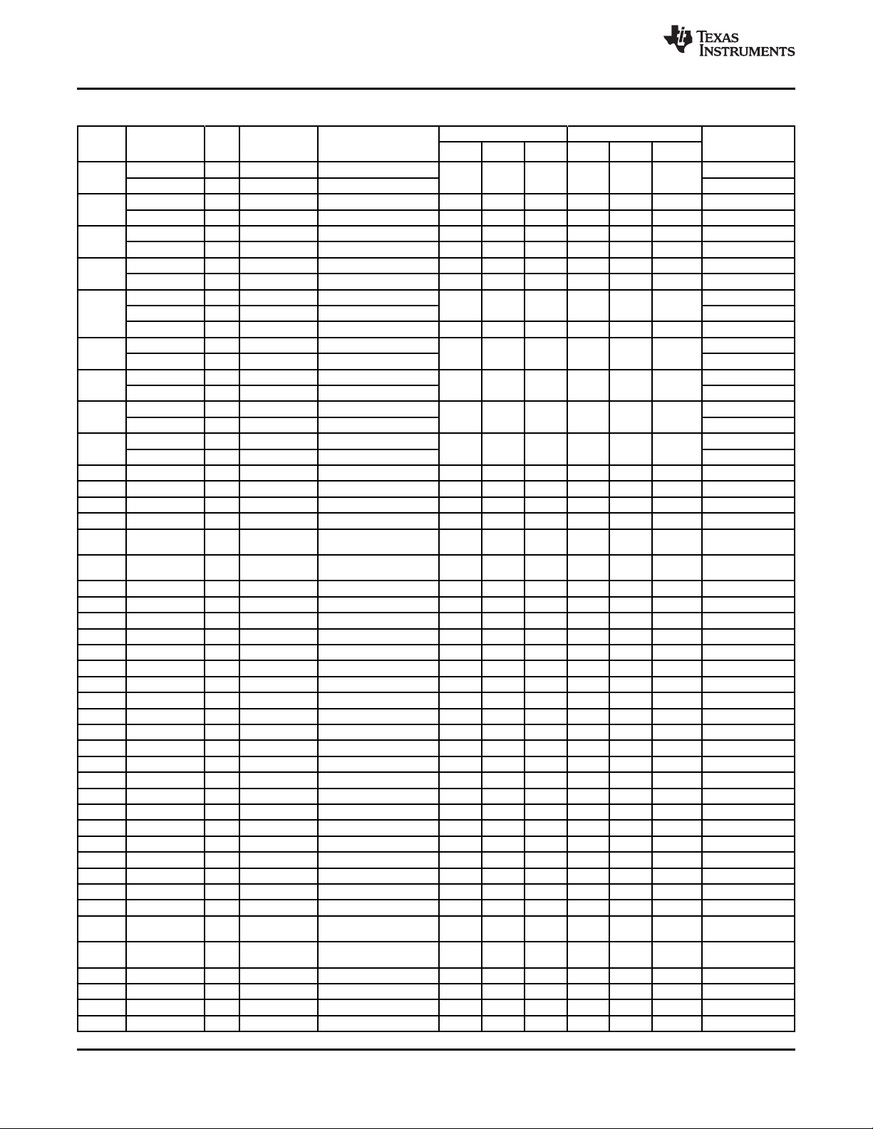
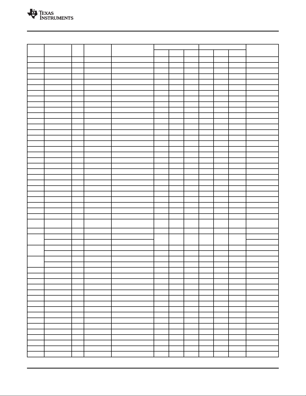
2.2 Ball Characteristics
Table 2-1 describes the terminal characteristics and the signals multiplexed on each pin. The following list
describes the column headings in Table 2-1:
1. Ball: Ball number(s) associated with each signal(s)
2. Pin Name: Names of all the signals that are multiplexed on each ball
3. A/D: Analog or digital signal
4. Type: Terminal type when a particular signal is multiplexed on the terminal
– I = Input
– O = Output
– OD = Open drain
5. Reference Level: Voltage applied to the I/O cell (see the power module and battery charger interface
[BCI] chapters for values).
6. PU/PD: Denotes the presence of an internal pullup or pulldown. Pullups and pulldowns can be enabled
or disabled through software.
7. Min = Minimum value
8. Typ = Typical value
9. Max = Maximum value
10. Buffer Strength: Drive strength of the associated output buffer
SWCS032E–OCTOBER 2008–REVISED JANUARY 2011
Table 2-1. Ball Characteristics
Ball[1] Type[4] Strength
H4 ADCIN0 A I/O VINTANA1.OUT
J3 ADCIN1 A I/O VINTANA1.OUT
G3 ADCIN2 A I VINTANA2.OUT
P5 VCCS A I VBAT + 0.2
N5 VAC A Power VACCHARGER
P4 VBATS A I VBAT
N4 PCHGAC A I VACCHARGER
N6 PCHGUSB A I VBUS
N2 VPRECH A O VPRECH
N1 BCIAUTO A I VPRECH
P6 ICTLUSB1 A O VBUS
P1 ICTLUSB2 A O VCCS
N7 ICTLAC1 A O VACCHARGER
P2 ICTLAC2 A O VCCS
R5 VBAT A Power VBAT
P12 75 100 202 59 100 144
N12 75 100 202 59 100 144
L4 156 220 450 59 100 144
P13 156 220 450 59 100 144
M4 PWM0 D O IO_1P8 75 100 202 59 100 144 4
Pin A/D Reference Level
Name[2] [3] RL[5]
GPIO0/CD1 D I/O IO_1P8 8
JTAG.TDO D I/O IO_1P8 8
GPIO1/CD2 D I/O IO_1P8 2
JTAG.TMS D I IO_1P8
GPIO2 D I/O IO_1P8 2
Test1 D I/O IO_1P8 2
GPIO15 D I/O IO_1P8 2
Test2 D I/O IO_1P8 2
GPIO6 D I/O IO_1P8 2
Test3 D I/O IO_1P8 2
PU[6] (kΩ) PD[6] (kΩ) Buffer
Min[7] Typ[8] Max[9] Min Typ Max
(mA)[10]
Copyright © 2008–2011, Texas Instruments Incorporated Terminal Description 15
Submit Documentation Feedback
Product Folder Link(s): TPS65950

TPS65950
SWCS032E–OCTOBER 2008–REVISED JANUARY 2011
www.ti.com
Table 2-1. Ball Characteristics (continued)
Ball[1] Type[4] Strength
N14 75 100 202 59 100 144
J9 START.ADC D I IO_1P8
C13 SYSEN D OD/I IO_1P8 4.7 7.35 10 2
C6 CLKEN D O IO_1P8 2
D7 CLKEN2 D O IO_1P8 2
G10 CLKREQ D I IO_1P8 60 100 146
F10 INT1 D O IO_1P8 2
F9 INT2 D O IO_1P8 2
A13 NRESPWRON D O IO_1P8 2
B13 NRESWARM D I IO_1P8 2
A11 PWRON D I VBAT
B14 NC
P7 NSLEEP1 D I IO_1P8
G9 NSLEEP2 D I IO_1P8
D13 CLK256FS
F8 VMODE1 D I IO_1P8
K11 BOOT0 A/D I/O VBAT
J11 BOOT1 A/D I/O VBAT
A10 REGEN D OD VBAT 5.5 8 12 2
H8 MSECURE D I IO_1P8
N16 VREF A Power VREF
N15 AGND A Power GND GND
C4
D6
D4 I2C.CNTL.SDA D I/O IO_1P8 2.5 3.4 12
D5 I2C.CNTL.SCL D I IO_1P8 2.5 3.4 12
R1 PCM.VCK D I/O IO_1P8 2
T2 PCM.VDR D I/O IO_1P8 2
T15 PCM.VDX D I/O IO_1P8 2
R16 PCM.VFS D I/O IO_1P8 2
L3 I2S.CLK D I/O IO_1P8 2
K6 I2S.SYNC D I/O IO_1P8 2
K4 I2S.DIN D I IO_1P8 2
K3 I2S.DOUT D O IO_1P8 2
E2 MIC.MAIN.P A I MICBIAS1.OUT
F2 MIC.MAIN.M A I MICBIAS1.OUT
G2
H2
E3 HSMIC.P A I VINTANA2.OUT
F3 HSMIC.M A I VINTANA2.OUT
D10 VBAT.LEFT A Power VBAT
D9 VBAT.LEFT A Power VBAT
B9 IHF.LEFT.P A O VBAT
B10 IHF.LEFT.M A O VBAT
C10 GND.LEFT A Power GND GND
C9 GND.LEFT A Power GND GND
D12 VBAT.RIGHT A Power VBAT
Pin A/D Reference Level
Name[2] [3] RL[5]
GPIO7 D I/O IO_1P8 2
VIBRA.SYNC D I IO_1P8
PWM1 D O IO_1P8 4
Test4 D I/O IO_1P8 2
(1)
NC
I2C.SR.SDA D I/O IO_1P8 2.5 3.4 12
VMODE2 D I IO_1P8 2
I2C.SR.SCL D I/O IO_1P8 2.5 3.4 12
MIC.SUB.P A I MICBIAS2.OUT
DIG.MIC.0 A I VMIC1.OUT
MIC.SUB.M A I MICBIAS2.OUT
DIG.MIC.1 A I VMIC2.OUT
D O IO_1P8 2
(1) To avoid reflection on this pin caused by impedance mismatch, a serial resistance (Rs) of 33 Ω must be added.
16 Terminal Description Copyright © 2008–2011, Texas Instruments Incorporated
Submit Documentation Feedback
Product Folder Link(s): TPS65950
PU[6] (kΩ) PD[6] (kΩ) Buffer
Min[7] Typ[8] Max[9] Min Typ Max
(mA)[10]
TPS65950
www.ti.com
SWCS032E–OCTOBER 2008–REVISED JANUARY 2011
Table 2-1. Ball Characteristics (continued)
Ball[1] Type[4] Strength
D11 VBAT.RIGHT A Power VBAT
B11 IHF.RIGHT.P A O VBAT
B12 IHF.RIGHT.M A O VBAT
C12 GND.RIGHT A Power GND GND
C11 GND.RIGHT A Power GND GND
A6 EAR.P A O VINTANA2.OUT
A7 EAR.M A O VINTANA2.OUT
B4 HSOL A O VINTANA2.OUT
B7
B5 HSOR A O VINTANA2.OUT
B8
F1 AUXL A I VINTANA2.OUT
G1 AUXR A I VINTANA2.OUT
D1
D2
E4 VHSMIC.OUT A Power VINTANA2.OUT
D3 MICBIAS.GND PowerGND GND
J4 / J6 /J7 /
J8 / E5
R10 AVSS2 A Power GND GND
M15 AVSS3 A Power GND GND
C7 AVSS4 A Power GND GND
B1 UART1.TXD D OD External 1.8 to 3.3 V 2
D8
N11
P11
N8
N9
L10 MANU D I VUSB.3P1 162 280 414
N10 32KCLKOUT D O IO_1P8
P16 32KXIN A I IO_1P8
P15 32KXOUT A O IO_1P8
A14 HFCLKIN A I IO_1P8
R12 HFCLKOUT D O IO_1P8
R8 VBUS A Power VBUS
T10 DP/UART3.RXD A I/O VBUS 2
T11 DN/UART3.TXD A I/O VBUS 2
R11 ID A I/O VBUS 2
L15 UCLK D I IO_1P8 16
L14 75 100 202 59 100 144
L13 75 100 202 59 100 144
Pin A/D Reference Level
Name[2] [3] RL[5]
PreDriv.LEFT A O VINTANA2.OUT
VMID A Power VINTANA2.OUT
PreDriv.RIGHT A O VINTANA2.OUT
ADCIN7 A I VINTANA2.OUT
MICBIAS1.OUT A Power VINTANA2.OUT
VMIC1.OUT A Power VINTANA2.OUT
MICBIAS2.OUT A Power VINTANA2.OUT
VMIC2.OUT A Power VINTANA2.OUT
AVSS1 A Power GND GND
GPIO8 D I IO_1P8 4.7 7.4 10 5.9 7 8.3
UART1.RXD D I IO_1P8
RTSO/
CLK64K.OUT/ D OD VUSB.3P1 2
BERCLK.OUT
ADCIN5 A I VINTANA2.OUT
CTSI/
BERDATA.OUT
ADCIN3 A I VINTANA2.OUT
TXAF A I VUSB.3P1
ADCIN4 A I VINTANA2.OUT
RXAF A O VUSB.3P1
ADCIN6 A I VINTANA2.OUT
STP D I IO_1P8 16
GPIO9 D I/O IO_1P8 2
DIR D O IO_1P8 16
GPIO10 D I/O IO_1P8 2
D OD/CMOS/I/O VUSB.3P1 4.7 7.4 10 2
PU[6] (kΩ) PD[6] (kΩ) Buffer
Min[7] Typ[8] Max[9] Min Typ Max
(mA)[10]
Copyright © 2008–2011, Texas Instruments Incorporated Terminal Description 17
Submit Documentation Feedback
Product Folder Link(s): TPS65950
TPS65950
SWCS032E–OCTOBER 2008–REVISED JANUARY 2011
Table 2-1. Ball Characteristics (continued)
Ball[1] Type[4] Strength
M13 75 100 202 59 100 144
K14
K13
J14
J13 UART4.CTSO D O IO_1P8 16
G14 75 100 202 59 100 144
G13 75 100 202 59 100 144
F14 75 100 202 59 100 144
F13 75 100 202 59 100 144
T16 TEST.RESET A/D I VBAT 30 50 70
T1 TESTV1 A I/O VBAT
A16 TESTV2 A I/O VINTANA2.OUT
A1 TEST D I IO_1P8 60 100 146
A15 D I IO_1P8
B16 D I IO_1P8
R7 CP.IN A Power VBAT/VBUS
T7 CP.CAPP A O CP.CAPP
T6 CP.CAPM A O CP.CAPM
R6 CP.GND A Power GND GND
R9 VBAT.USB A Power VBAT
P9 VUSB.3P1 A Power VUSB.3P1
L1 VAUX12S.IN A Power VBAT
M2 VAUX1.OUT A Power VAUX1.OUT
M3 VAUX2.OUT A Power VAUX2.OUT
H15 VPLLA3R.IN A Power VBAT
K16 VRTC.OUT A Power VRTC.OUT
H14 VPLL1.OUT A Power VPLL1.OUT
J15 VSDI.CSI.OUT A Power VSDI.CSI.OUT
G16 VAUX3.OUT A Power VAUX3.OUT
B2 VAUX4.IN A Power VBAT
B3 VAUX4.OUT A Power VAUX4.OUT
C1 VMMC1.IN A Power VBAT
C2 VMMC1.OUT A Power VMMC1.OUT
A3 VMMC2.IN A Power VBAT
A4 VMMC2.OUT A Power VMMC2.OUT
K2 VSIM.OUT A Power VSIM.OUT
P8 A Power VINTUSB1P5.OUT
P10 A Power VINTUSB1P8.OUT
K1 VDAC.IN A Power VBAT
L2 VDAC.OUT A Power VDAC.OUT
K15 VINT.IN A Power VBAT
H3 VINTANA1.OUT A Power VINTANA1.OUT
Pin A/D Reference Level
Name[2] [3] RL[5]
NXT D O IO_1P8 16
GPIO11 D I/O IO_1P8 2
DATA0 D I/O IO_1P8 16
UART4.TXD D I IO_1P8
DATA1 D I/O IO_1P8 16
UART4.RXD D O IO_1P8 2
DATA2 D I/O IO_1P8 16
UART4.RTSI D I IO_1P8
DATA3 D I/O IO_1P8 16
GPIO12 D I/O IO_1P8 75 100 202 59 100 144 16
DATA4 D I/O IO_1P8 16
GPIO14 D I/O IO_1P8 2
DATA5 D I/O IO_1P8 16
GPIO3 D I/O IO_1P8 2
DATA6 D I/O IO_1P8 16
GPIO4 D I/O IO_1P8 2
DATA7 D I/O IO_1P8 16
GPIO5 D I/O IO_1P8 2
JTAG.TDI/
BERDATA
JTAG.TCK/
BERCLK
VINTUSB1P5.
OUT
VINTUSB1P8.
OUT
PU[6] (kΩ) PD[6] (kΩ) Buffer
Min[7] Typ[8] Max[9] Min Typ Max
60 100 140 60 100 140
(mA)[10]
www.ti.com
18 Terminal Description Copyright © 2008–2011, Texas Instruments Incorporated
Submit Documentation Feedback
Product Folder Link(s): TPS65950
TPS65950
www.ti.com
SWCS032E–OCTOBER 2008–REVISED JANUARY 2011
Table 2-1. Ball Characteristics (continued)
Ball[1] Type[4] Strength
J2 VINTANA2.OUT A Power VINTANA2.OUT
B6 VINTANA2.OUT A Power VINTANA2.OUT
L16 VINTDIG.OUT A Power VINTDIG.OUT
E15 VDD1.IN A Power VBAT
E14 VDD1.IN A Power VBAT
D14 VDD1.IN A Power VBAT
D16 VDD1.SW A O VBAT
D15 VDD1.SW A O VBAT
C14 VDD1.SW A O VBAT
E13 VDD1.FB A I
C16 VDD1.GND A Power GND GND
C15 VDD1.GND A Power GND GND
B15 VDD1.GND A Power GND GND
R13 VDD2.IN A Power VBAT
P14 VDD2.IN A Power VBAT
N13 VDD2.FB A I
T13 VDD2.SW A O VBAT
R14 VDD2.SW A O VBAT
T14 VDD2.GND A Power GND GND
R15 VDD2.GND A Power GND GND
P3 VIO.IN A Power VBAT
R4 VIO.IN A Power VBAT
N3 VIO.FB A I
R3 VIO.SW A O VBAT
T4 VIO.SW A O VBAT
R2 VIO.GND A Power GND GND
T3 VIO.GND A Power GND GND
M14 BKBAT A Power VBACK
C8 IO.1P8 A Power IO_1P8
H13 / H9 /
H10 / H11
F16 LEDGND A Power GND GND
G11 75 100 202 59 100 144
F15
G15
G8 KPD.C0 D OD IO_1P8
H7 KPD.C1 D OD IO_1P8
G6 KPD.C2 D OD IO_1P8
F7 KPD.C3 D OD IO_1P8
G7 KPD.C4 D OD IO_1P8
F4 KPD.C5 D OD IO_1P8
H6 KPD.C6 D OD IO_1P8
G4 KPD.C7 D OD IO_1P8
K9 KPD.R0 D I IO_1P8 8 10 12
K8 KPD.R1 D I IO_1P8 8 10 12
L8 KPD.R2 D I IO_1P8 8 10 12
K7 KPD.R3 D I IO_1P8 8 10 12
L9 KPD.R4 D I IO_1P8 8 10 12
J10 KPD.R5 D I IO_1P8 8 10 12
K10 KPD.R6 D I IO_1P8 8 10 12
L7 KPD.R7 D I IO_1P8 8 10 12
Pin A/D Reference Level
Name[2] [3] RL[5]
DGND A Power GND GND
GPIO13 D I/O IO_1P8
LEDSYNC D I IO_1P8
LEDA A OD VBAT
VIBRA.P A OD VBAT
LEDB A OD VBAT
VIBRA.M A OD VBAT
PU[6] (kΩ) PD[6] (kΩ) Buffer
Min[7] Typ[8] Max[9] Min Typ Max
(mA)[10]
Copyright © 2008–2011, Texas Instruments Incorporated Terminal Description 19
Submit Documentation Feedback
Product Folder Link(s): TPS65950
TPS65950
SWCS032E–OCTOBER 2008–REVISED JANUARY 2011
www.ti.com
Table 2-1. Ball Characteristics (continued)
Ball[1] Type[4] Strength
C3 BT.PCM.VDR D I/O IO_1P8 75 100 202 59 100 144
C5 BT.PCM.VDX D I/O IO_1P8 75 100 202 59 100 144
A2 RFID.EN D O VMMC2.OUT
Pin A/D Reference Level
Name[2] [3] RL[5]
GPIO16 D I/O IO_1P8
DIG.MIC.CLK0 D O IO_1P8
GPIO17 D I/O IO_1P8
DIG.MIC.CLK1 D O IO_1P8
PU[6] (kΩ) PD[6] (kΩ) Buffer
Min[7] Typ[8] Max[9] Min Typ Max
(mA)[10]
2.3 Signal Description
Table 2-2 lists the signals on the TPS65950; some signals are available on multiple pins.
Table 2-2. Signal Description
Configuration By Default After Reset
Module Description Type
Signal Unused
Name Features
(1)
Ball
Signal Type
ADCIN0 Battery type I/O H4 ADCIN0 I GND
ADC ADCIN1 Battery temperature I/O J3 ADCIN1 I GND
ADCIN2 General-purpose (GP) ADC input I G3 ADCIN2 I GND
VCCS Charge current sensing I P5 VCCS I Cap to GND
VAC Charge device input voltage Power N5 VAC Power GND
VBATS Charge current sensing I P4 VBATS I Cap to GND
PCHGAC I N4 PCHGAC I GND
ac precharge sense signal. Used
also for EEPROM
PCHGUSB USB precharge sense signal I N6 PCHGUSB I GND
Charger
VPRECH Precharge regulator output O N2 VPRECH O Cap to GND
BCIAUTO Linear charge specific boot mode I N1 BCIAUTO I GND
ICTLUSB1 USB power device control O P6 ICTLUSB1 O Floating
ICTLUSB2 USB power device control O P1 ICTLUSB2 O Floating
ICTLAC1 ac power device control O N7 ICTLAC1 O Floating
ICTLAC2 ac power device control O P2 ICTLAC2 O Floating
VBAT Battery voltage sensing Power R5 VBAT Power VBAT
GPIOs/
JTAG
GPIO0/CD1 GPIO0/card detection 1 I/O
JTAG.TDO JTAG test data output I/O
GPIO1/CD2 GPIO1/card detection 2 I/O
JTAG.TMS JTAG test mode state I
GPIO2 GPIO2 I/O
Test1 Test1 pin used in test mode only I/O
GPIO15 GPIO15 I/O
Test2 Test2 pin used in test mode only I/O
GPIO6 GPIO6 I/O
PWM0 Pulse width driver 0 O
Test3 I/O
Test3 pin used in test mode only
(controlled by JTAG)
P12 GPIO0 I PD Floating
N12 GPIO1 I PD Floating
L4 GPIO2 I PD Floating
P13 GPIO15 I PD Floating
M4 GPIO6 I PD Floating
GPIO7 GPIO7 I/O
VIBRA.SYNC Vibrator on-off synchronization I
N14 GPIO7 I PD Floating
START.
ADC
PWM1 Pulse width driver O
Test4 I/O
Test4 pin used in test mode only
(controlled by JTAG)
START.ADC ADC conversion request I J9 START.ADC I GND
Released
(1)
Internal
Pull or Not
(2)
(3)
(3)
(3)
20 Terminal Description Copyright © 2008–2011, Texas Instruments Incorporated
Submit Documentation Feedback
Product Folder Link(s): TPS65950
TPS65950
www.ti.com
SWCS032E–OCTOBER 2008–REVISED JANUARY 2011
Table 2-2. Signal Description (continued)
Configuration By Default After Reset
Module Description Type
CONTROL
VREF
I2C
SmartReflex
I2C
PCM
TDM
ANA.MIC G2 MIC.SUB.P I Cap to GND
Headset
microphone
Signal Unused
Name Features
SYSEN System enable output OD/I C13 SYSEN OD PU Floating
CLKEN Clock enable O C6 CLKEN O Floating
CLKEN2 Clock enable 2 O D7 CLKEN2 O Floating
CLKREQ Clock request I G10 CLKREQ I PD GND
INT1 Output interrupt line 1 O F10 INT1 O Floating
INT2 Output interrupt line 2 O F9 INT2 O Floating
NRESPWRON O A13 NRESPWRON O Floating
NRESWARM I B13 NRESWARM I GND
PWRON I A11 PWRON I VBAT
NC Not connected B14 NC Floating
NSLEEP1 Sleep request from device 1 I P7 NSLEEP1 I GND
NSLEEP2 Sleep request from device 2 I G9 NSLEEP2 I GND
CLK256FS Control for 256 × FSCLK output O D13 CLK256FS O Floating
VMODE1 I F8 VMODE1 I GND
BOOT0 Boot pin 0 I K11 BOOT0 I PD N/A
BOOT1 Boot pin 1 I J11 BOOT1 I PD N/A
REGEN Enable signal for external LDO OD A10 REGEN OD PU Floating
MSECURE I H8 MSECURE I N/A
VREF Reference voltage Power N16 VREF Power N/A
AGND N15 AGND Power GND GND
NC Not connected
I2C.SR.SDA I/O
VMODE2 I
I2C.SR.SCL I/O
I2C.CNTL.SDA I/O D4 I2C.CNTL.SDA I/O PU N/A
I2C.CNTL.SCL I/O D5 I2C.CNTL.SCL I/O PU N/A
PCM.VCK Data clock (voice port) I/O R1 PCM.VCK I/O Floating
PCM.VDR Data receive (voice port) I/O T2 PCM.VDR I/O GND
PCM.VDX Data transmit (voice port) I/O T15 PCM.VDX I/O Floating
PCM.VFS Frame synchronization (voice port) I/O R16 PCM.VFS I/O Floating
I2S.CLK Clock signal (audio port) I/O L3 I2S.CLK I/O Floating
I2S.SYNC Synchronization signal (audio port) I/O K6 I2S.SYNC I/O Floating
I2S.DIN Data receive (audio port) I K4 I2S.DIN I GND
I2S.DOUT Data transmit (audio port) O K3 I2S.DOUT O Floating
MIC.MAIN.P Main microphone left input (P) I E2 MIC.MAIN.P I Cap to GND
MIC.MAIN.M Main microphone left input (M) I F2 MIC.MAIN.M I Cap to GND
MIC.SUB.P Main microphone right input (P) I
DIG.MIC.0 Digital microphone 0 input data I
MIC.SUB.M Main microphone right input (M) I
DIG.MIC.1 Digital microphone 1 input data I
HSMIC.P Headset microphone input (P) I E3 HSMIC.P I Cap to GND
HSMIC.M Headset microphone input (M) I F3 HSMIC.M I Cap to GND
Output control the NRESPWRON
of the application processor
Input, detect user action on the
reset button
Input, detect a control command to
start or stop the system
Digital voltage scaling linked with
VDD1
Security and digital rights
management
Analog ground for reference Power
voltage GND
SmartReflex I2C data
Digital voltage scaling linked with
VDD2
SmartReflex I2C data
GP I2C data
GP I2C clock
(1)
Ball
Signal Type
Signal not
C4 Floating
D6 VMODE2 I GND
H2 MIC.SUB.M I Cap to GND
functional
(4)
Released
(1)
Internal
Pull or Not
(2)
Copyright © 2008–2011, Texas Instruments Incorporated Terminal Description 21
Submit Documentation Feedback
Product Folder Link(s): TPS65950
TPS65950
SWCS032E–OCTOBER 2008–REVISED JANUARY 2011
Table 2-2. Signal Description (continued)
Module Description Type
Hands-free
Earpiece
Headset
AUX input
VMIC BIAS
Headset
UART
Signal Unused
Name Features
VBAT.LEFT Battery voltage input Power D10 VBAT.LEFT Power VBAT
VBAT.LEFT Battery voltage input Power D9 VBAT.LEFT Power VBAT
IHF.LEFT.P Hands-free speaker output left (P) O B9 IHF.LEFT.P O Floating
IHF.LEFT.M Hands-free speaker output left (M) O B10 IHF.LEFT.M O Floating
GND.LEFT GND C10 GND.LEFT Power GND GND
GND.LEFT GND C9 GND.LEFT Power GND GND
VBAT.RIGHT Battery voltage input Power D12 VBAT.RIGHT Power VBAT
VBAT.RIGHT Battery voltage input Power D11 VBAT.RIGHT Power VBAT
GND.RIGHT GND C12 GND.RIGHT Power GND GND
GND.RIGHT GND C11 GND.RIGHT Power GND GND
IHF.RIGHT.P Hands-free speaker output right (P) O B11 IHF.RIGHT.P O Floating
IHF.RIGHT.M O B12 IHF.RIGHT.M O Floating
EAR.P O A6 EAR.P O Floating
EAR.M O A7 EAR.M O Floating
HSOL O B4 HSOL O Floating
PreDriv.LEFT O
VMID Pseudo-ground for headset output Power
HSOR O B5 HSOR O Floating
PreDriv.RIGHT O
ADCIN7 GP ADC input 7 I
AUXL Auxiliary audio input left I F1 AUXL I Cap to GND
AUXR Auxiliary audio input right I G1 AUXR I Cap to GND
MICBIAS1.
OUT
VMIC1.OUT Digital microphone power supply 1 Power
MICBIAS2.
OUT
VMIC2.OUT Digital microphone power supply 2 Power
VHSMIC.OUT Headset microphone bias Power E4 VHSMIC.OUT Power Floating
MICBIAS.GND Dedicated ground for microphones D3 MICBIAS.GND Power GND GND
AVSS1 AVSS1
AVSS2 R10 AVSS2
AVSS3 M15 AVSS3
AVSS4 C7 AVSS4
UART1.TXD Headset UART transmit data OD B1 UART1.TXD OD PU Floating
GPIO8 GPIO8 I/O
UART1.RXD receiver/transmitter (UART) receive I
Hands-free speaker output right
(M)
Earpiece output differential output
(P)
Earpiece output differential output
(M)
Differential/single-ended headset
left output
Predriver output left P for external
class-D amplifier
Differential/single-ended headset
right output (P)
Predriver output right P for external
class-D amplifier
Analog microphone bias 1 Power
Analog microphone bias 2 Power
Analog ground Power GND GND
Headset universal asynchronous
data/switch detection
Power
GND
Power
GND
Power
GND
Power
GND
Power
GND
Power
GND
Configuration By Default After Reset
(1)
Ball
Signal Type
B7 VMID Power Floating
B8 ADCIN7 I GND
D1 MICBIAS1.OUT Power Floating
D2 MICBIAS2.OUT Power Floating
J4/J6/
J7/J8/E5
D8 GPIO8 I PD Floating
Released
(1)
Internal
Pull or Not
www.ti.com
(2)
22 Terminal Description Copyright © 2008–2011, Texas Instruments Incorporated
Submit Documentation Feedback
Product Folder Link(s): TPS65950
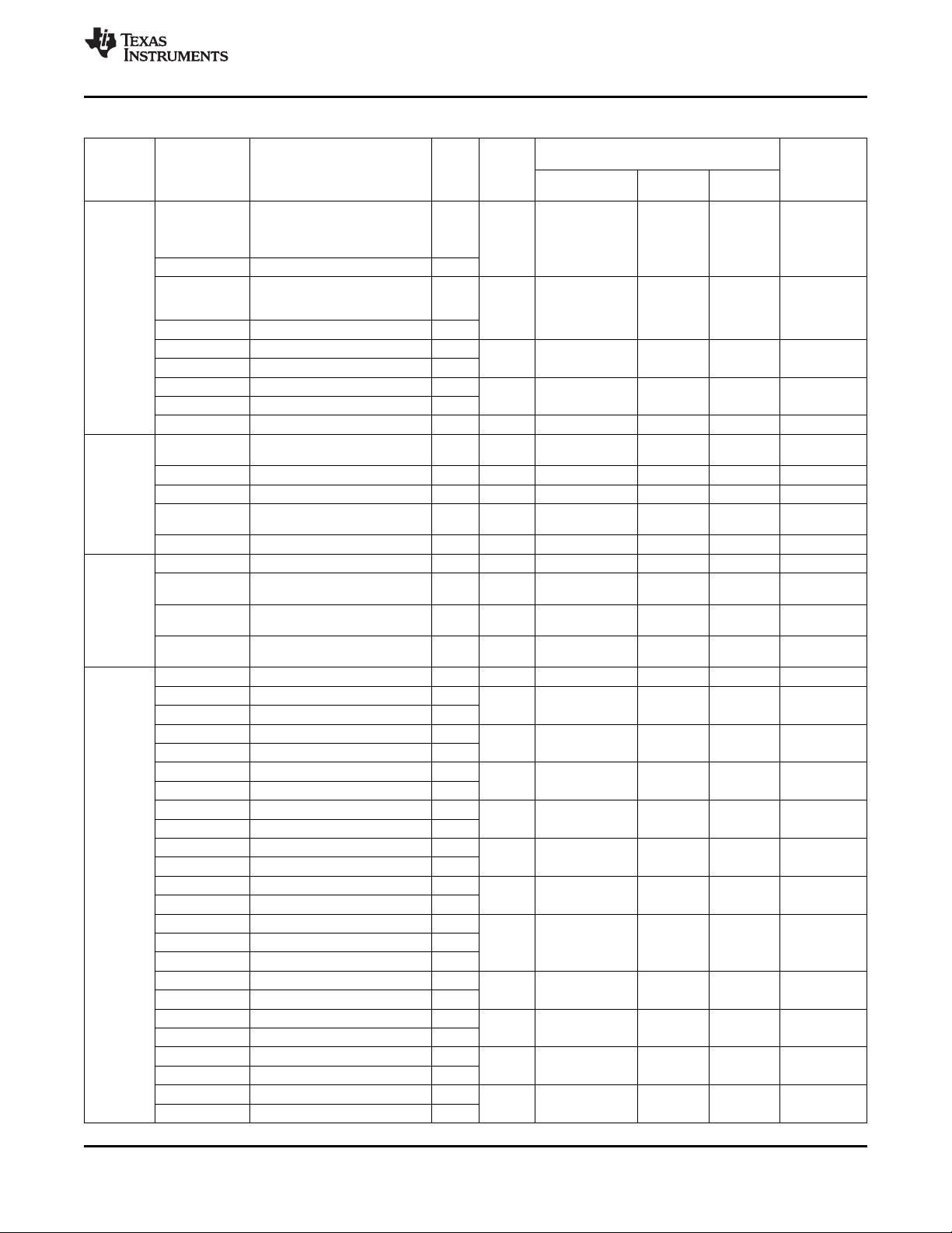
TPS65950
www.ti.com
SWCS032E–OCTOBER 2008–REVISED JANUARY 2011
Table 2-2. Signal Description (continued)
Configuration By Default After Reset
Module Description Type
MCPC
Clock 32KXOUT Output of the 32-kHz oscillator O P15 32KXOUT O Floating
USB PHY
ULPI J14 DATA2 O Floating
Signal Unused
Name Features
RTSO/
CLK64K.OUT/ OD
BERCLK.OUT
ADCIN5 GP ADC input 5 I
CTSI/ Clear-to-send input/
BERDATA.OUT BERDATAOUT in test mode
ADCIN3 GP ADC input 3 I
TXAF I
ADCIN4 GP ADC input 4 I
RXAF O
ADCIN6 GP ADC input 6 I
MANU Manufacturer pin I L10 MANU I PU Floating
32KCLKOUT O N10 32KCLKOUT O Floating
32KXIN Input of the 32-kHz oscillator I P16 32KXIN I N/A
HFCLKIN I A14 HFCLKIN I N/A
HFCLKOUT HS clock output O R12 HFCLKOUT O Floating
VBUS VBUS power rail Power R8 VBUS Power N/A
DP/ UART3.RXD I/O T10 DP/UART3.RXD I/O N/A
DN/ UART3.TXD I/O T11 DN/UART3.TXD I/O N/A
ID USB ID I/O R11 ID I/O
UCLK HS USB clock I L15 UCLK O Floating
STP HS USB stop I
GPIO9 GPIO9 I/O
DIR HS USB direction O
GPIO10 GPIO10 I/O
NXT HS USB next O
GPIO11 GPIO11 I/O
DATA0 HS USB Data0 I/O
UART4.TXD UART4.TXD I
DATA1 HS USB Data1 I/O
UART4.RXD UART4.RXD O
DATA2 HS USB Data2 I/O
UART4.RTSI UART4.RTSI I
DATA3 HS USB Data3 I/O
UART4.CTSO UART4.CTSO O J13 DATA3 O Floating
GPIO12 GPIO12 I/O
DATA4 HS USB Data4 I/O
GPIO14 GPIO14 I/O
DATA5 HS USB Data5 I/O
GPIO3 GPIO3 I/O
DATA6 HS USB Data6 I/O
GPIO4 GPIO4 I/O
DATA7 HS USB Data7 I/O
GPIO5 GPIO5 I/O
Ready-to-send output/
64-kHz output clock/
Bit error ratio (BER) clock out in
test mode
Buffered output of the 32-kHz
digital clock
Input of the digital (or sine) HS
clock
USB data P/USB carkit receive
data/UART3 receive data
USB data N/USB carkit transmit
data/UART3 transmit data
OD/
CMOS/
I/O
(1)
Ball
Signal Type
RTSO/
N11 CLK64K.OUT/ OD Floating
BERCLK.OUT
CTSI/
P11 OD GND
BERDATA.OUT
N8 TXAF I Cap to GND
N9 RXAF O Floating
L14 STP I PU Floating
L13 DIR O Floating
M13 NXT O Floating
K14 DATA0 O Floating
K13 DATA1 O Floating
G14 DATA4 O Floating
G13 DATA5 O Floating
F14 DATA6 O Floating
F13 DATA7 O Floating
Released
(1)
Internal
Pull or Not
Connected to
VRUSB3V1
(2)
Copyright © 2008–2011, Texas Instruments Incorporated Terminal Description 23
Submit Documentation Feedback
Product Folder Link(s): TPS65950
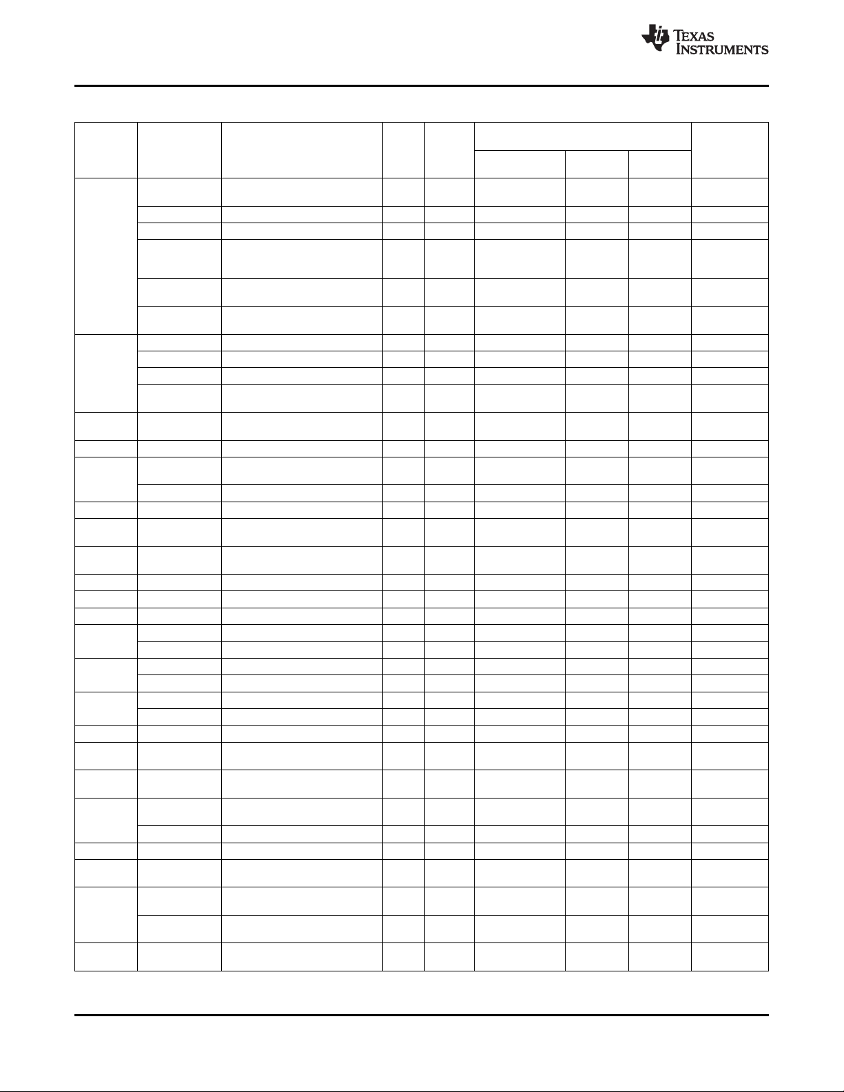
TPS65950
SWCS032E–OCTOBER 2008–REVISED JANUARY 2011
www.ti.com
Table 2-2. Signal Description (continued)
Configuration By Default After Reset
Module Description Type
Test
USB CP
VBAT.USB VBAT.USB Power R9 VBAT.USB Power VBAT
USB.LDO VUSB.3P1 USB LDO output Power P9 VUSB.3P1 Power N/A
VAUX1
VAUX2 VAUX2.OUT VAUX2 LDO output voltage Power M3 VAUX2.OUT Power Floating
VPLLA3R VPLLA3R.IN Power H15 VPLLA3R.IN Power VBAT
VRTC VRTC.OUT Power K16 VRTC.OUT Power N/A
VPLL1 VPLL1.OUT LDO output voltage Power H14 VPLL1.OUT Power Floating
VPLL2 VSDI.CSI.OUT Output voltage of the regulator Power J15 VSDI.CSI.OUT Power Floating
VAUX3 VAUX3.OUT VAUX3 LDO output voltage Power G16 VAUX3.OUT Power Floating
VAUX4
VMMC1
VMMC2
VSIM VSIM.OUT VSIM LDO output voltage Power K2 VSIM.OUT Power Floating
VINTUSB1 VINTUSB1P5. VINTUSB1P5 internal LDO output VINTUSB1P5.
P5 OUT (internal use only) OUT
VINTUSB1 VINTUSB1P8. VINTUSB1P8 internal LDO output VINTUSB1P8.
P8 OUT (internal use only) OUT
Video DAC
VINT VINT.IN Input for VINTDIG LDO Power K15 VINT.IN Power VBAT
VINTANA1 Power H3 VINTANA1.OUT Power N/A
VINTANA2
VINTDIG VINTDIG.OUT Power L16 VINTDIG.OUT Power N/A
Signal Unused
Name Features
Test.RESET I T16 Test.RESET I PD GND
TestV1 Analog test I/O T1 TestV1 I/O Floating
TestV2 Analog test I/O A16 TestV2 I/O Floating
Test application mode for JTAG/GPIOs I A1 Test I PD Floating
JTAG.TDI/ JTAG.TDI/
BERDATA BERDATA
JTAG.TCK/ JTAG.TCK/
BERCLK BERCLK
CP.IN CP input voltage Power R7 CP.IN Power VBAT
CP.CAPP CP flying capacitor P O T7 CP.CAPP O Floating
CP.CAPM CP flying capacitor M O T6 CP.CAPM O Floating
CP.GND CP ground R6 CP.GND Power GND GND
VAUX12S.IN Power L1 VAUX12S.IN Power VBAT
VAUX1.OUT VAUX1 LDO output voltage Power M2 VAUX1.OUT Power Floating
VAUX4.IN VAUX4 LDO input voltage Power B2 VAUX4.IN Power VBAT
VAUX4.OUT VAUX4 LDO output voltage Power B3 VAUX4.OUT Power Floating
VMMC1.IN VMMC1 LDO input voltage Power C1 VMMC1.IN Power VBAT
VMMC1.OUT VMMC1 LDO output voltage Power C2 VMMC1.OUT Power Floating
VMMC2.IN VMMC2 LDO input voltage Power A3 VMMC2.IN Power VBAT
VMMC2.OUT VMMC2 LDO output voltage Power A4 VMMC2.OUT Power Floating
VDAC.IN Power K1 VDAC.IN Power VBAT
VDAC.OUT Output voltage of the regulator Power L2 VDAC.OUT Power Floating
VINTANA1. VINTANA1 internal LDO output
OUT (internal use only)
VINTANA2. VINTANA2 internal LDO output
OUT (internal use only)
VINTANA2. VINTANA2 internal LDO output
OUT (internal use only)
Reset T2 device (except power
state-machine)
Selection between JTAG mode and
(with PU or PD)
JTAG.TDI/BERDATA I A15 I GND
JTAG.TCK/BERCLK I B16 I GND
USB LDOs (VINTUSB1P5,
VINTUSB1P8, VUSB.3P1) VBAT
VAUX1/VAUX2/VSIM LDO input
voltage
Input for VPLL1, VPLL2, VAUX3,
VRTC LDOs
VRTC internal LDO output (internal
use only)
Input for VDAC, VINTANA1, and
VINTANA2 LDOs
VINTDIG internal LDO output
(internal use only)
(1)
Ball
Signal Type
Power
GND
Power P8 Power Floating
Power P10 Power Floating
Power J2 VINTANA2.OUT Power N/A
Power B6 VINTANA2.OUT Power N/A
Released
(1)
Internal
Pull or Not
(2)
24 Terminal Description Copyright © 2008–2011, Texas Instruments Incorporated
Submit Documentation Feedback
Product Folder Link(s): TPS65950
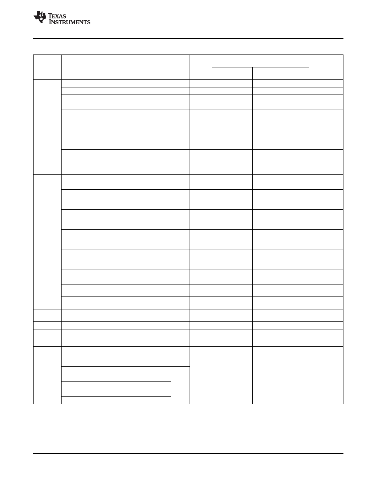
TPS65950
www.ti.com
SWCS032E–OCTOBER 2008–REVISED JANUARY 2011
Table 2-2. Signal Description (continued)
Configuration By Default After Reset
Module Description Type
VDD1
VDD2
VIO
Backup
battery
Digital VDD IO.1P8 TPS65950 I/O input Power C8 IO.1P8 Power N/A
Digital Power
ground GND
LED driver
Signal Unused
Name Features
VDD1.IN VDD1 dc-dc input voltage Power E15 VDD1.IN Power VBAT
VDD1.IN VDD1 dc-dc input voltage Power E14 VDD1.IN Power VBAT
VDD1.IN VDD1 dc-dc input voltage Power D14 VDD1.IN Power VBAT
VDD1.SW VDD1 dc-dc switch O D16 VDD1.SW O Floating
VDD1.SW VDD1 dc-dc switch O D15 VDD1.SW O Floating
VDD1.SW VDD1 dc-dc switch O C14 VDD1.SW O Floating
VDD1.FB I E13 VDD1.FB I GND
VDD1.GND VDD1 dc-dc ground C16 VDD1.GND Power GND GND
VDD1.GND VDD1 dc-dc ground C15 VDD1.GND Power GND GND
VDD1.GND VDD1 dc-dc ground B15 VDD1.GND Power GND GND
VDD2.IN VDD2 dc-dc input voltage Power R13 VDD2.IN Power VBAT
VDD2.IN VDD2 dc-dc input voltage Power P14 VDD2.IN Power VBAT
VDD2.FB I N13 VDD2.FB I GND
VDD2.SW VDD2 dc-dc switch O T13 VDD2.SW O Floating
VDD2.SW VDD2 dc-dc switch O R14 VDD2.SW O Floating
VDD2.GND VDD2 dc-dc ground T14 VDD2.GND Power GND GND
VDD2.GND VDD2 dc-dc ground R15 VDD2.GND Power GND GND
VIO.IN VIO dc-dc input voltage Power P3 VIO.IN Power VBAT
VIO.IN VIO dc-dc input voltage Power R4 VIO.IN Power VBAT
VIO.FB I N3 VIO.FB I GND
VIO.SW VIO dc-dc switch O R3 VIO.SW O Floating
VIO.SW VIO dc-dc switch O T4 VIO.SW O Floating
VIO.GND VIO dc-dc ground R2 VIO.GND Power GND GND
VIO.GND VIO dc-dc ground T3 VIO.GND Power GND GND
BKBAT Backup battery Power M14 BKBAT Power GND
DGND Digital ground / H10 / DGND Power GND GND
LEDGND LED driver ground F16 LEDGND Power GND GND
GPIO13 GPIO13 I/O
LEDSYNC LED synchronization input I
LEDA LED leg A
VIBRA.P H-bridge vibrator P
LEDB LED leg B
VIBRA.M H-bridge vibrator M
VDD1 dc-dc output voltage
(feedback)
VDD2 dc-dc output voltage
(feedback)
VIO dc-dc output voltage
(feedback)
(1)
Ball
Signal Type
Power
GND
Power
GND
Power
GND
Power
GND
Power
GND
Power
GND
Power
GND
H13 / H9
H11
Power
GND
G11 GPIO13 I PD Floating
OD F15 Floating
OD G15 Floating
Signal not
functional
Signal not
functional
(4)
(4)
Released
(1)
Internal
Pull or Not
(2)
Copyright © 2008–2011, Texas Instruments Incorporated Terminal Description 25
Submit Documentation Feedback
Product Folder Link(s): TPS65950
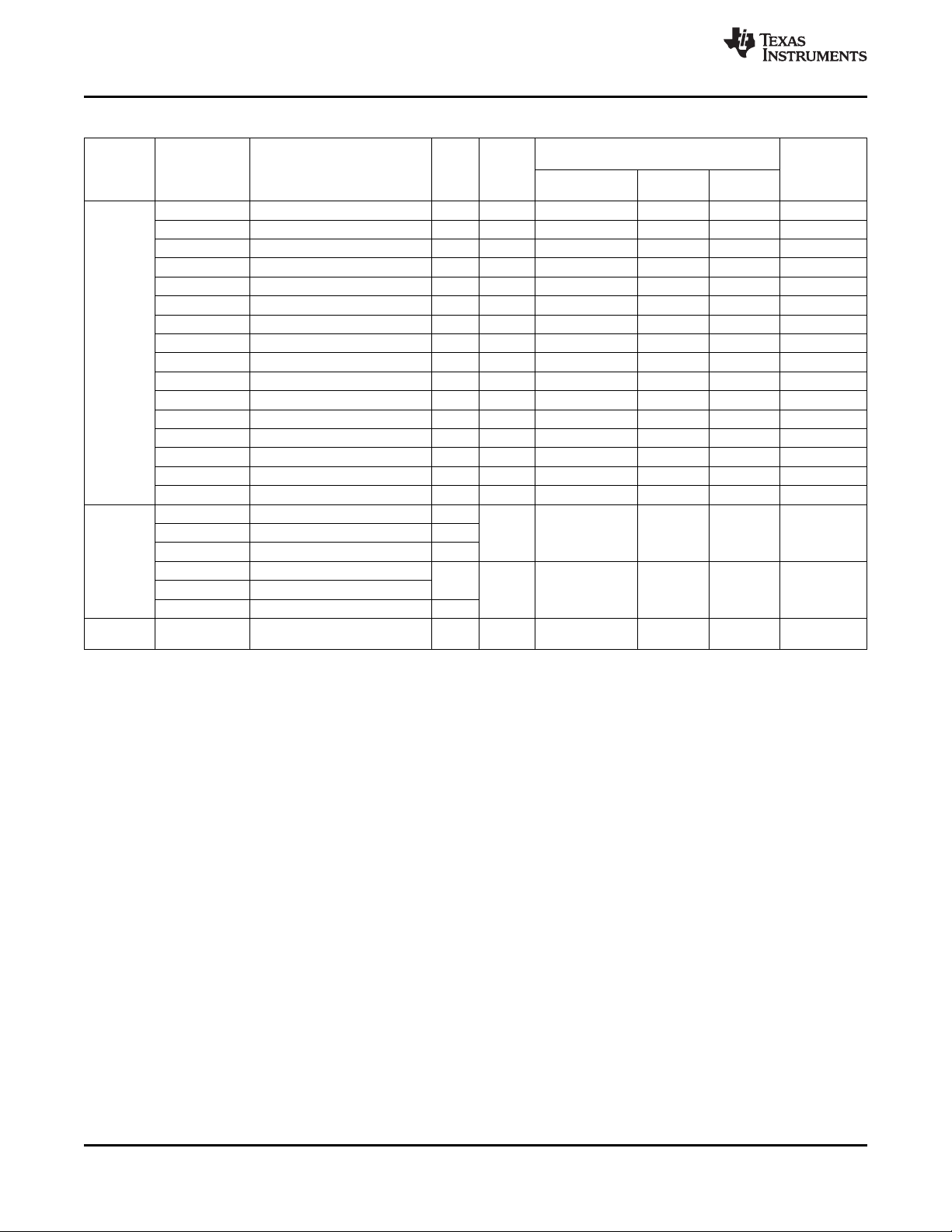
TPS65950
SWCS032E–OCTOBER 2008–REVISED JANUARY 2011
www.ti.com
Table 2-2. Signal Description (continued)
Configuration By Default After Reset
Module Description Type
Keypad
Bluetooth/
digital
microphone
RFID RFID.EN O A2 RFID.EN O Floating
Signal Unused
Name Features
KPD.C0 Keypad column 0 OD G8 KPD.C0 OD Floating
KPD.C1 Keypad column 1 OD H7 KPD.C1 OD Floating
KPD.C2 Keypad column 2 OD G6 KPD.C2 OD Floating
KPD.C3 Keypad column 3 OD F7 KPD.C3 OD Floating
KPD.C4 Keypad column 4 OD G7 KPD.C4 OD Floating
KPD.C5 Keypad column 5 OD F4 KPD.C5 OD Floating
KPD.C6 Keypad column 6 OD H6 KPD.C6 OD Floating
KPD.C7 Keypad column 7 OD G4 KPD.C7 OD Floating
KPD.R0 Keypad row 0 I K9 KPD.R0 I PU Floating
KPD.R1 Keypad row 1 I K8 KPD.R1 I PU Floating
KPD.R2 Keypad row 2 I L8 KPD.R2 I PU Floating
KPD.R3 Keypad row 3 I K7 KPD.R3 I PU Floating
KPD.R4 Keypad row 4 I L9 KPD.R4 I PU Floating
KPD.R5 Keypad row 5 I J10 KPD.R5 I PU Floating
KPD.R6 Keypad row 6 I K10 KPD.R6 I PU Floating
KPD.R7 Keypad row 7 I L7 KPD.R7 I PU Floating
GPIO16 Bluetooth PCM receive data I/O
BT.PCM.VDR GPIO16 I/O C3 GPIO16 I PD Floating
DIG.MIC.CLK0 Digital microphone clock 0 O
GPIO17 GPIO17
BT.PCM.VDX Bluetooth PCM transmit data C5 GPIO17 I PD Floating
DIG.MIC.CLK1 Digital microphone clock 1 O
Enable for the radio frequency
identification (RFID) device
I/O
(1)
Ball
Signal Type
(1) I = Input; O = Output; OD = Open drain
(2) This column provides the connection when the associated feature is not used or not connected. When there is a pin muxing, not all
functions on the muxed pin are used. But even if a function is not used, the Default Configuration column applies.
Connection criteria:
– Analog pins:
– For input: GND
– For output: Floating (except VPRECH is connected to GND)
– For I/O if input by default: GND (except for audio features input: capacitor to ground with a 100-nF typical value capacitor)
– Digital pins:
– For input: GND (except keypad and STP are left floating)
– For input and pullup: Floating
– For output: Floating
– For I/O and pullup: Floating
N/A (not applicable): When the associated feature is mandatory for good functioning of the TPS65950.
(3) The VPRECH, VBATS, and VCCS signals must be connected to each other and with the CPRECH capacitor to GND (see
Configuration with BCI Not Used).
(4) Signal not functional indicates that no signal is presented on the pad after a release reset.
Released
(1)
Internal
Pull or Not
Section 8.2.3
(2)
,
26 Terminal Description Copyright © 2008–2011, Texas Instruments Incorporated
Submit Documentation Feedback
Product Folder Link(s): TPS65950
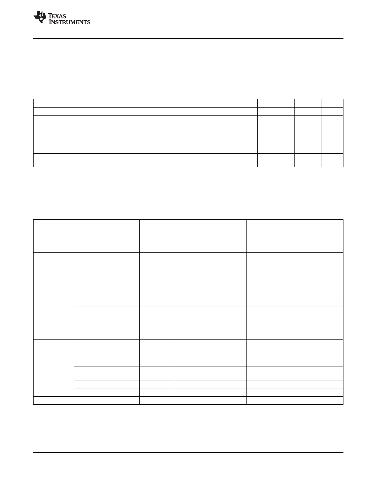
TPS65950
www.ti.com
SWCS032E–OCTOBER 2008–REVISED JANUARY 2011
3 Electrical Characteristics
3.1 Absolute Maximum Ratings
Table 3-1 lists the absolute maximum ratings.
Table 3-1. Absolute Maximum Ratings
Parameter Test Conditions Min Typ Max Unit
Main battery supply voltage
Voltage on any input Where supply represents the voltage applied to 0.0 1.0*Supply V
Storage temperature range –55 125 °C
Ambient temperature range –40 85 °C
Junction temperature (TJ) At 1.4W (Theta JB 11°C/W 2S2P board) 105 °C
Junction temperature (TJ) for parametric –40 105 °C
compliance
(1) The product can tolerate voltage spikes of 5.2 V for a total duration of 10 milliseconds.
3.2 Minimum Voltages and Associated Currents
Table 3-2 lists the VBAT minimum and maximum currents per VBAT ball.
Table 3-2. VBAT Min Required Per VBAT Ball and Associated Maximum Current
(1)
the power supply pin associated with the input
2.1 4.5 V
Category Pin and Module Maximum Output Voltage (V) VBAT Minimum (V)
VBAT pin name VDD_VPLLA3R_IN_6POV 340
VPLL1 (LDO) 40 1.0 / 1.2 / 1.3 / 1.8 / 2.8 / 3.0 Maximum
VPLL2 (LDO) 100 0.7 / 1.0 / 1.2 / 1.3 / 1.5 / 1.8 / Maximum
Internal module
supplied
VBAT pin name VDD_VDAC_IN_6POV 370
Internal module
supplied VINTANA2 (LDO) 250 2.5 / 2.75 Maximum
VBAT pin name VDD_VAUXI2S_IN_6POV 350
VAUX3 (LDO) 200 1.5 / 1.8 / 2.5 / 2.8 / 3.0 Maximum
VDD1 core (DCDC) < 1 2.7
VDD2 core (DCDC) < 1 2.7
SYSPOR (power ref) < 1 2.7
PBIAS (power ref) < 1 2.7
VDAC (LDO) 70 1.2 / 1.3 / 1.8 Maximum
VINTANA1 (LDO) 50 1.5 Maximum
VIO core (DCDC) < 1 2.7
VAUX4 core (LDO) < 1 2.7
Current
Specified
(mA)
(2.7, output voltage selected + 250 mV)
1.85 / 2.5 / 2.6 / 2.8 / 2.85 / 3.0 (2.7, output voltage selected + 250 mV)
/ 3.15
(2.7, output voltage selected + 250 mV)
(2.7, output voltage selected + 250 mV)
(2.7, output voltage selected + 250 mV)
(2.7, output voltage selected +250 mV)
Copyright © 2008–2011, Texas Instruments Incorporated Electrical Characteristics 27
Submit Documentation Feedback
Product Folder Link(s): TPS65950
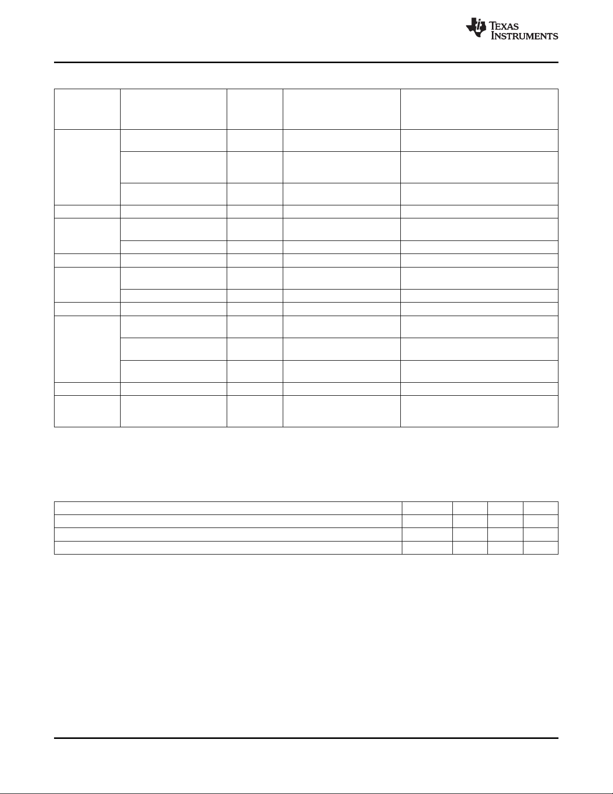
TPS65950
SWCS032E–OCTOBER 2008–REVISED JANUARY 2011
Table 3-2. VBAT Min Required Per VBAT Ball and Associated Maximum Current (continued)
Category Pin and Module Maximum Output Voltage (V) VBAT Minimum (V)
VAUX1 (LDO) 200 1.5 / 1.8 / 2.5 / 2.8 / 3.0 Maximum
Internal module
supplied
VBAT pin name VDD_VMMC2_IN_6POV 100
VBAT pin name VDD_VMMC1_IN_6POV 220
VBAT pin name VDD_VINT_IN_6POV 131
Internal module VRRTC (LDO) 30 1.5 Maximum
supplied (2.7, output voltage selected + 250 mV)
VBAT pin name VDD_VAUX4_IN_6POV 100
VAUX2 (LDO) 100 1.3 / 1.5 / 1.6 / 1.7 / 1.8 / 1.9 / Maximum
VSIM (LDO) 50 1.0 / 1.2 / 1.3 / 1.8 / 2.8 / 3.0 Maximum
VMMC2 (LDO) 100 1.0 / 1.2 / 1.3 / 1.5 / 1.8 / 1.85 / Maximum
Power_REGBATT 0.001 2.7
VMMC1 (LDO) 220 1.85 / 2.85 / 3.0 / 3.15 Maximum
Power_REGBATT 0.001 2.7
VINTDIG (LDO) 80 1.0 / 1.2 / 1.3 / 1.5 Maximum
VBACKUP (LDO) 1 2.5 / 3.0 / 3.1 / 3.2 Maximum
VAUX4 (LDO) 100 0.7 / 1.0 / 1.2 / 1.3 / 1.5 / 1.8 / output voltage selected + 250 mV
Current
Specified
(mA)
(2.7, output voltage selected + 250 mV)
2.0 / 2.1 / 2.2 / 2.3 / 2.4 / 2.5 / (2.7, output voltage selected + 250 mV)
2.8
(2.7, output voltage selected + 250 mV)
2.5 / 2.6 / 2.8 / 2.85 / 3.0 / 3.15 (2.7, output voltage selected + 250 mV)
(2.7, output voltage selected + 250 mV)
(2.7, output voltage selected + 250 mV)
(2.7, output voltage selected + 250 mV)
1.85 / 2.5 / 2.6 / 2.8 / 2.85 / 3.0
/ 3.15
www.ti.com
3.3 Recommended Operating Conditions
Table 3-3 lists the recommended operating maximum ratings.
Table 3-3. Recommended Operating Maximum Ratings
Parameter Min Typ Max Unit
Main battery supply voltage 2.7
Backup battery supply voltage 1.8 3.2 3.3 V
Ambient temperature range –40 85 °C
(1) 2.7 V is the minimum threshold for the battery at which the device will turn OFF. However, the minimum voltage at which the device will
power ON is 3.2 V ±100 mV (if PWRON does not have a switch and is connected to VBAT) considering battery plug as the device
switch on event. If PWRON has a switch then 3.2 V is the minimum for the device to turn ON.
(1)
3.6 4.5 V
3.4 Digital I/O Electrical Characteristics
Table 3-4 describes the digital I/O electrical characteristics.
• RL: Reference level voltage applied to the I/O cell
• VOL: Low-level output voltage
• VOH: High-level output voltage
• VIL: Low-level input voltage
• VIH: High-level input voltage
28 Electrical Characteristics Copyright © 2008–2011, Texas Instruments Incorporated
Submit Documentation Feedback
Product Folder Link(s): TPS65950
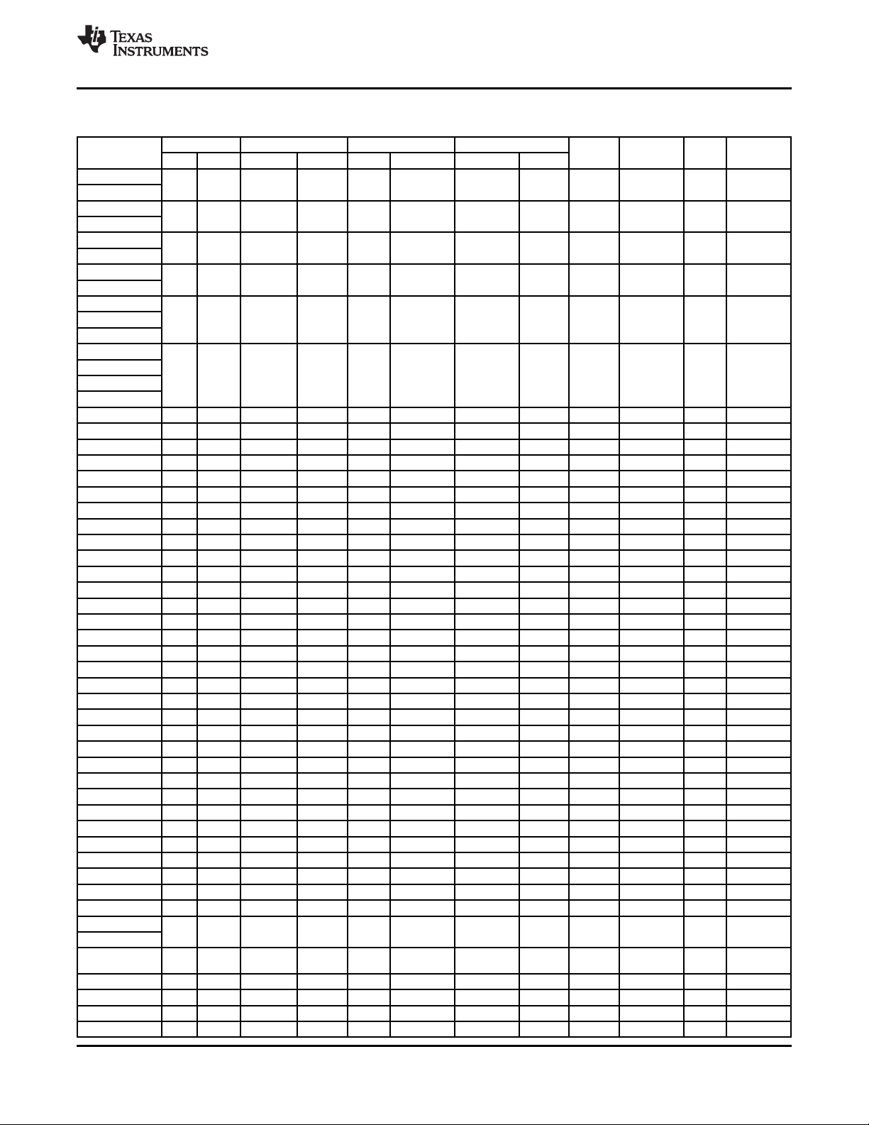
TPS65950
www.ti.com
SWCS032E–OCTOBER 2008–REVISED JANUARY 2011
Table 3-4. Digital I/O Electrical Characteristics
Pin Name Fall Time (ns)
GPIO0/CD1
JTAG.TDO
GPIO0/CD2
JTAG.TMS
GPIO2
Test1
GPIO15
Test2
GPIO16
PWM0 0 0.45 RL–0.45 RL 0 0.35xRL 0.65xRL RL 3 30 5.2 5.2
Test3
GPIO17
VIBRA.SYNC
PWM1
Test4
START.ADC 0 0.45 RL–0.45 RL 0 0.35×RL 0.65×RL RL 6 16.7 16.7
SYSEN 0 0.45 RL–0.45 RL 0 0.35×RL 0.65×RL RL 5.2 5.2
CLKEN 0 0.45 RL–0.45 RL 0 0.35×RL 0.65×RL RL 3 30 33.3 33.3
CLKEN2 0 0.45 RL–0.45 RL 0 0.35×RL 0.65×RL RL 3 30 33.3 33.3
CLKREQ 0 0.45 RL–0.45 RL 0 0.35×RL 0.65×RL RL 3 33.3 33.3
INT1 0 0.45 RL–0.45 RL 0 0.35×RL 0.65×RL RL 3 30 33.3 33.3
INT2 0 0.45 RL–0.45 RL 0 0.35×RL 0.65×RL RL 3 30 33.3 33.3
NRESPWRON 0 0.45 RL–0.45 RL 0 0.35×RL 0.65×RL RL 3 30 33.3 33.3
NRESWARM 0 0.45 RL–0.45 RL 0 0.35×RL 0.65×RL RL 3 30 33.3 33.3
PWRON 0 0.35×1.8V 0.65×1.8V VBAT 3 33.3 33.3
NSLEEP1 0 0.45 RL–0.45 RL 0 0.35×RL 0.65×RL RL 3 33.3 33.3
NSLEEP2 0 0.45 RL–0.45 RL 0 0.35×RL 0.65×RL RL 3 33.3 33.3
CLK256FS 0 0.45 RL–0.45 RL 0 0.35×RL 0.65×RL RL 12.288 30 16.3 16.3
VMODE1 0 0.45 RL–0.45 RL 0 0.35×RL 0.65×RL RL 3 33.3 33.3
BOOT0 0 RL 3 33.3 33.3
BOOT1 0 RL 3 33.3 33.3
REGEN 0 0.45 RL–0.45 RL 0 0.35×RL 0.65×RL RL 3 30 33.3 33.3
MSECURE 0 0.45 RL–0.45 RL 0 0.35×RL 0.65×RL RL 3 33.3 33.3
I2C.SR.SDA 0 0.4 –0.5 0.3×RL 0.7×RL RL+0.5 3.4 Up to 400
VMODE2 0 0.45 RL–0.45 RL 0 0.35×RL 0.65×RL RL 3.4 29.4 29.4
I2C.SR.SCL 0 0.4 –0.5 0.3×RL 0.7×RL RL+0.5 3.4 10.0 10.0
I2C.CNTL.SDA 0 0.4 –0.5 0.3×RL 0.7×RL RL+0.5 3.4 Up to 400
I2C.CNTL.SCL 0 0.4 –0.5 0.3×RL 0.7×RL RL+0.5 3.4 10.0 10.0
PCM.VCK 0 0.45 RL–0.45 RL 0 0.35×RL 0.65×RL RL 1 30 100.0 33.0
PCM.VDR 0 0.45 RL–0.45 RL 0 0.35×RL 0.65×RL RL 1 30 100.0 100.0
PCM.VDX 0 0.45 RL–0.45 RL 0 0.35×RL 0.65×RL RL 1 30 100.0 33.0
PCM.VFS 0 0.45 RL–0.45 RL 0 0.35×RL 0.65×RL RL 1 30 33.0 33.0
I2S.CLK 0 0.45 RL–0.45 RL 0 0.35×RL 0.65×RL RL 6.5 30 33.0 33.0
I2S.SYNC 0 0.45 RL–0.45 RL 0 0.35×RL 0.65×RL RL 6.5 30 33.0 33.0
I2S.DIN 0 0.45 RL–0.45 RL 0 0.35×RL 0.65×RL RL 3.25 30 33.0 33.0
I2S.DOUT 0 0.45 RL–0.45 RL 0 0.35×RL 0.65×RL RL 3.25 30 29.0 29.0
UART1.TXD 0 0.45 RL–0.45 RL 0 0.35×RL 0.65×RL RL 3 30 33.0 33.0
GPIO8
UART1.RXD
RTSO/CLD64K.OUT/
BERCLK.OUT
CTSI/BERDATA.OUT 0 0.45 RL–0.45 RL 0 0.35×RL 0.65×RL RL 3 30 33.0 33.0
MANU 0 0.45 RL–0.45 RL 0 0.35×RL 0.65×RL RL 3 33.0 33.0
32KCLKOUT 0 0.45 RL–0.45 RL 0 0.35×RL 0.65×RL RL 0.032 30 16 16
HFCLKOUT 0 0.45 RL–0.45 RL 0 0.35×RL 0.65×RL RL 38.4 30 2.6 2.6
VOL (V) VOH (V) VIL (V) VIH (V)
Min Max Min Max Min Max Min Max
0 0.45 RL–0.45 RL 0 0.35xRL 0.65xRL RL 33 30 5.2 5.2
0 0.45 RL–0.45 RL 0 0.35xRL 0.65xRL RL 33 30 5.2 5.2
0 0.45 RL–0.45 RL 0 0.35xRL 0.65xRL RL 3 30 5.2 5.2
0 0.45 RL–0.45 RL 0 0.35xRL 0.65xRL RL 3 30 5.2 5.2
0 0.45 RL–0.45 RL 0 0.35xRL 0.65xRL RL 3 30 5.2 5.2
0 0.45 RL–0.45 RL 0 0.35×RL 0.65×RL RL 3 33.0 33.0
0 0.45 RL–0.45 RL 0 0.35×RL 0.65×RL RL 3 30 33.0 33.0
Max Freq Load (pF) Rise
(MHz) Output Mode Time (ns)
Copyright © 2008–2011, Texas Instruments Incorporated Electrical Characteristics 29
Submit Documentation Feedback
Product Folder Link(s): TPS65950
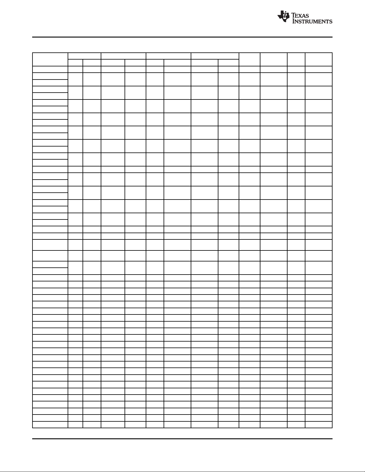
TPS65950
SWCS032E–OCTOBER 2008–REVISED JANUARY 2011
www.ti.com
Table 3-4. Digital I/O Electrical Characteristics (continued)
Pin Name Fall Time (ns)
UCLK 0 0.45 RL–0.45 RL 0 0.35×RL 0.65×RL RL 60 10 1.0 1.0
STP
GPIO9
DIR
GPIO10
NXT
GPIO11
DATA0
UART4.TXD
DATA1
UART4.RXD
DATA2
UART4.RTSI
DATA3
UART4.CTSO
GPIO12 0 0.45 RL–0.45 RL 0 0.35×RL 0.65×RL RL 30 10 1.0 1.0
DATA4
GPIO14
DATA5
GPIO3
DATA6
GPIO4
DATA7
GPIO5
Test.RESET 0 0.45 RL–0.45 RL 0 0.35×RL 0.65×RL RL 3 33.0 33.0
Test 0 0.45 RL–0.45 RL 0 0.35×RL 0.65×RL RL 3 30 29.0 29.0
JTAG.TDI/
BERDATA
JTAG.TCK/
BERDATA
GPIO13
LEDSYNC
KPD.C0 0 0.45 RL–0.45 RL 0 0.35×RL 0.65×RL RL 0.033 30 29.0 29.0
KPD.C1 0 0.45 RL–0.45 RL 0 0.35×RL 0.65×RL RL 0.033 30 29.0 29.0
KPD.C2 0 0.45 RL–0.45 RL 0 0.35×RL 0.65×RL RL 0.033 30 29.0 29.0
KPD.C3 0 0.45 RL–0.45 RL 0 0.35×RL 0.65×RL RL 0.033 30 29.0 29.0
KPD.C4 0 0.45 RL–0.45 RL 0 0.35×RL 0.65×RL RL 0.033 30 29.0 29.0
KPD.C5 0 0.45 RL–0.45 RL 0 0.35×RL 0.65×RL RL 0.033 30 29.0 29.0
KPD.C6 0 0.45 RL–0.45 RL 0 0.35×RL 0.65×RL RL 0.033 30 29.0 29.0
KPD.C7 0 0.45 RL–0.45 RL 0 0.35×RL 0.65×RL RL 0.033 30 29.0 29.0
KPD.R0 0 0.45 RL–0.45 RL 0 0.35×RL 0.65×RL RL 0.033 3051.8 3051.8
KPD.R1 0 0.45 RL–0.45 RL 0 0.35×RL 0.65×RL RL 0.033 3051.8 3051.8
KPD.R2 0 0.45 RL–0.45 RL 0 0.35×RL 0.65×RL RL 0.033 3051.8 3051.8
KPD.R3 0 0.45 RL–0.45 RL 0 0.35×RL 0.65×RL RL 0.033 3051.8 3051.8
KPD.R4 0 0.45 RL–0.45 RL 0 0.35×RL 0.65×RL RL 0.033 3051.8 3051.8
KPD.R5 0 0.45 RL–0.45 RL 0 0.35×RL 0.65×RL RL 0.033 3051.8 3051.8
KPD.R6 0 0.45 RL–0.45 RL 0 0.35×RL 0.65×RL RL 0.033 3051.8 3051.8
KPD.R7 0 0.45 RL–0.45 RL 0 0.35×RL 0.65×RL RL 0.033 3051.8 3051.8
GPIO16 0 0.45 RL–0.45 RL 0 0.35×RL 0.65×RL RL 3 30 33.3 33.3
DIG.MIC.CLK0 0 0.45 RL–0.45 RL 0 0.35×RL 0.65×RL RL 2.4 30 41.7 41.7
BT.PCM.VDX 0 0.45 RL–0.45 RL 0 0.35×RL 0.65×RL RL 1 30 100.0 100.0
GPIO17 0 0.45 RL–0.45 RL 0 0.35×RL 0.65×RL RL 3 30 33.3 33.3
DIG.MIC.CLK1 0 0.45 RL–0.45 RL 0 0.35×RL 0.65×RL RL 2.4 30 41.7 41.7
BT.PCM.VDX 0 0.45 RL–0.45 RL 0 0.35×RL 0.65×RL RL 1 30 100.0 100.0
RFID.EN
VOL (V) VOH (V) VIL (V) VIH (V)
Min Max Min Max Min Max Min Max
0 0.45 RL–0.45 RL 0 0.35×RL 0.65×RL RL 30 10 1.0 1.0
0 0.45 RL–0.45 RL 0 0.35×RL 0.65×RL RL 30 10 1.0 1.0
0 0.45 RL–0.45 RL 0 0.35×RL 0.65×RL RL 30 10 1.0 1.0
0 0.45 RL–0.45 RL 0 0.35×RL 0.65×RL RL 30 10 1.0 1.0
0 0.45 RL–0.45 RL 0 0.35×RL 0.65×RL RL 30 10 1.0 1.0
0 0.45 RL–0.45 RL 0 0.35×RL 0.65×RL RL 30 10 1.0 1.0
0 0.45 RL–0.45 RL 0 0.35×RL 0.65×RL RL 30 10 1.0 1.0
0 0.45 RL–0.45 RL 0 0.35×RL 0.65×RL RL 30 10 1.0 1.0
0 0.45 RL–0.45 RL 0 0.35×RL 0.65×RL RL 30 10 1.0 1.0
0 0.45 RL–0.45 RL 0 0.35×RL 0.65×RL RL 30 10 1.0 1.0
0 0.45 RL–0.45 RL 0 0.35×RL 0.65×RL RL 30 10 1.0 1.0
0 0.45 RL–0.45 RL 0 0.35×RL 0.65×RL RL 3 33.0 33.0
0 0.45 RL–0.45 RL 0 0.35×RL 0.65×RL RL 3 33.0 33.0
0 0.45 RL–0.45 RL 0 0.35×RL 0.35×RL 3 30 33.3 33.3
Max Freq Load (pF) Rise
(MHz) Output Mode Time (ns)
30 Electrical Characteristics Copyright © 2008–2011, Texas Instruments Incorporated
Submit Documentation Feedback
Product Folder Link(s): TPS65950

TPS65950
www.ti.com
SWCS032E–OCTOBER 2008–REVISED JANUARY 2011
Copyright © 2008–2011, Texas Instruments Incorporated Electrical Characteristics 31
Submit Documentation Feedback
Product Folder Link(s): TPS65950

TPS65950
SWCS032E–OCTOBER 2008–REVISED JANUARY 2011
4 Power Module
This section describes the electrical characteristics of the voltage regulators and timing characteristics of
the supplies digitally controlled in the TPS65950.
Figure 4-1 is a block diagram of the power provider.
www.ti.com
32 Power Module Copyright © 2008–2011, Texas Instruments Incorporated
Submit Documentation Feedback
Product Folder Link(s): TPS65950

VRUSB_1V8
1.81 V
30 mA
VRUSB_3V1
3.1 V
15 mA
Main battery
VPLL2.OUT
VIO.L
VIO.OUT
VIO.GND
VIO.IN x 2
VDD2.L
VDD2.OUT
VDD2.GND
(2)
(2)
VDD2
(DC-DC)
0.6 V to 1.5 V
600 mA
VDD2.IN x 2
VMMC1
1.85/2.85
/3.0/3.15 V
220 mA
VMMC1.OUT
VMMC2
1.0/1.2/1.3/1.5/1.8/1.85/
2.5/2.6/2.8/2.85
/3.0/3.15 V
100 mA
VMMC2.OUT
VAUX1
1.5/1.8/2.5/2.8/3.0 V
200 mA
VAUX1.OUT
VAUX2
1.3/1.5/1.7/1.8/1.9/2.0/
2.1/2.2/2.3/2.4/2.5/2.8 V
100 mA
VAUX2.OUT
VAUX3
1.5/1.8/2.5/2.8/3.0 V
200 mA
VAUX3.OUT
VAUX4
0.7/1.0/1.2/1.3/1.5/1.8/
1.85/2.5/2.6/2.8/
2.85/3.0/3.15 V
100 mA
VAUX4.OUT
VPLL1
1.0/1.2/1.3/1.8 V
40 mA
VPLL1.OUT
VINTANA.OUT
VINTANA1
1.5V
50 mA
VINTDIG.OUT
VINTDIG
1.0/1.2/1.3/1.5 V
80 mA
VSIM.OUT
VDAC
1.2/1.3/1.8 V
70 mA
VDAC.OUT
VINTANA2.OUT
VINTANA2
2.5/2.75 V
250 mA
VDD1.L
VDD1.OUT
VDD1.GND
(3)
VDD1
(DC-DC)
0.6 V to 1.45 V
1200 mA
(See note)
VDD1.IN x 3
VUSB.3P1
VINTUSB1P8.OUT
VRUSB_1V5
1.525 V
30 mA
VINTUSB1P5.OUT
VIO
(DC-DC)
1.8 V/1.85 V
700 mA
(3)
(2)
(2)
032-002
CVINTDIG.OUT
CVINTANA1.OUT
CVINTANA2.OUT
CVDAC.OUT
CVSIM.OUT
LVDD1
CVDD1.OUT
LVDD2
CVDD2.OUT
LVIO
CVIO.OUT
VINT.IN
VDAC.IN
VDAC.IN
VDAC.IN
VAUX12S.IN
VPLLA3R.IN
VPLLA3R.IN
VMMC1.IN
VMMC2.IN
VAUX12S.IN
VAUX12S.IN
VPLLA3R.IN
VAUX4.IN
VBAT.USB
VBAT.USB
VBAT.USB
CVPLL1.OUT
CVPLL2.OUT
CVMMC1.OUT
CVMMC2.OUT
CVAUX1.OUT
CVAUX2.OUT
CVAUX3.OUT
CVAUX4.OUT
CVUSB.3P1
CVINTUSB1P8.OUT
CVINTUSB1P5.OUT
VPLL2
0.7/1.0/1.2/1.3/1.5/1.8/1.85
/2.5/2.6/2.8/2.85/3.0/3.15 V
100 mA
VSIM
1.0/1.2/1.3/
1.8/2.8/3.0 V
50 mA
TPS65950
www.ti.com
SWCS032E–OCTOBER 2008–REVISED JANUARY 2011
NOTE: For TPS65950A3: 0.6V to 1.2V, 1200mA and 1.2V to 1.45V, 1400mA
Figure 4-1. Power Provider Block Diagram
For the component values, see Table 15-1.
Copyright © 2008–2011, Texas Instruments Incorporated Power Module 33
Submit Documentation Feedback
Product Folder Link(s): TPS65950
NOTE

TPS65950
SWCS032E–OCTOBER 2008–REVISED JANUARY 2011
www.ti.com
4.1 Power Providers
Table 4-1 lists the power providers.
Table 4-1. Summary of the Power Providers
Default Voltage
Name Use Type Voltage Range (V)
VAUX1 External LDO 1.5, 1.8, 2.5, 2.8, 3.0 3.0 V 3.0 V 200 mA
VAUX2 External LDO 1.3, 1.5, 1.7, 1.8, 1.9, 2.0, 2.1, 2.2, 2.3, 2.4, 2.5, 2.8 2.8 V 1.8 V 100 mA
VAUX3 External LDO 1.5, 1.8, 2.5, 2.8, 3.0 2.8 V 2.8 V 200 mA
VAUX4 External LDO 1.2 V 2.8 V 100 mA
VMMC1 External LDO 1.85, 2.85, 3.0, 3.15 1.85 V 3.0 V 220 mA
VMMC2 External LDO 1.0, 1.2, 1.3, 1.5, 1.8, 1.85, 2.5, 2.6, 2.8, 2.85, 3.0, 3.15 2.6 V 2.6 V 100 mA
VPLL1 External LDO 1.0, 1.2, 1.3, 1.8, 2.8, 3.0 1.3 V 1.8 V 40 mA
VPLL2 External LDO 1.3 V 1.3 V 100 mA
VSIM External LDO 1.0, 1.2, 1.3, 1.8, 2.8, 3.0 1.8 V 1.8 V 50 mA
VDAC External LDO 1.2, 1.3, 1.8 1.8 V 1.8 V 70 mA
VIO External SMPS 1.8, 1.85 1.8 V 1.8 V 700 mA
VDD1 for
TPS65950A2/ External SMPS 0.6 ... 1.45 1.3 V 1.2 V 1200 mA
TPS65950A3
VDD1 for
TPS65950A3
VDD2 External SMPS 0.6 ... 1.5 1.3 V 1.2 V 600 mA
VINTANA1 Internal LDO 1.5 1.5 V 1.5 V 50 mA
VINTANA2 Internal LDO 2.5, 2.75 2.75 V 2.75 V 250 mA
VINTDIG Internal LDO 1.0, 1.2, 1.3, 1.5 1.5 V 1.5 V 80 mA
USBCP Internal CP 5 5 V 5 V 100 mA
VUSB1V5 Internal LDO 1.5 1.5 V 1.5 V 30 mA
VUSB1V8 Internal LDO 1.8 1.8 V 1.8 V 30 mA
VUSB3V1 Internal LDO 3.1 3.1 V 3.1 V 15 mA
VRRTC Internal LDO 1.5 1.5 V 1.5 V 30 mA
VBRTC Internal LDO 1.3 1.3 V 1.3 V 100 μA
External SMPS 1.2 ... 1.45 1.3 V 1.2 V 1400mA
0.7, 1.0, 1.2, 1.3 1.5, 1.8, 1.85, 2.5, 2.6, 2.8, 2.85, 3.0,
3.15
0.7, 1.0, 1.2, 1.3, 1.5, 1.8, 1.85, 2.5, 2.6, 2.8, 2.85, 3.0,
3.15
Depending on Boot Mode
OMAP2 OMAP3
Mode Mode
(1) For the significance of boot mode, see Section 4.5, Power Management.
(1)
Maximum
Current
34 Power Module Copyright © 2008–2011, Texas Instruments Incorporated
Submit Documentation Feedback
Product Folder Link(s): TPS65950
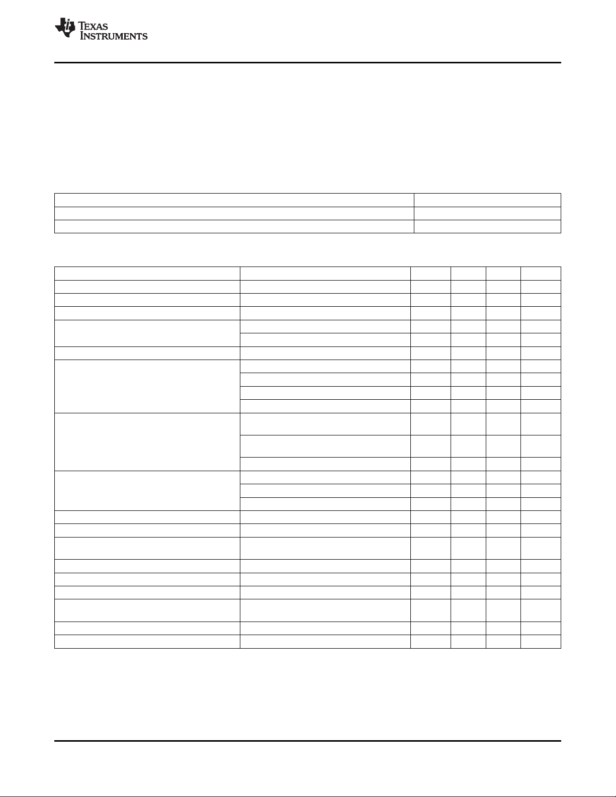
TPS65950
www.ti.com
SWCS032E–OCTOBER 2008–REVISED JANUARY 2011
4.1.1 VDD1 dc-dc Regulator
4.1.1.1 VDD1 dc-dc Regulator Characteristics
The VDD1 dc-dc regulator is a stepdown dc-dc converter with a configurable output voltage. The
programming of the output voltage and the characteristics of the dc-dc converter are
SmartReflex-compatible. The regulator can be put in sleep mode to reduce its leakage (PFM) or
power-down mode when it is not being used. Table 4-3 lists the characteristics of the regulator.
Table 4-2. Part Names With Corresponding VDD1 Current Support
Device Name VDD1 Current Support
TPS65950A2ZXN/R (some bug fixes, see errata) 1.2 A
TPS65950A3ZXN/R (same as TPS65950A2 + 1 GHz support with higher current support) 1.4 A
Table 4-3. VDD1 dc-dc Regulator Characteristics
Parameter Comments Min Typ Max Unit
Input voltage range 2.7 3.6 4.5 V
Output voltage 0.6 1.45 V
Output voltage step Covering the 0.6 to 1.45-V range 12.5 mV
Output accuracy
Switching frequency 3.2 MHz
Conversion efficiency
sleep modes
Output current Active mode, Output Voltage 1.2 V to1.45 V 1400 mA
Ground current (IQ) Off at 30°C 3 μA
Short-circuit current VIN= V
Load regulation 0 < IO< I
Transient load regulation
Line regulation 10 mV
Transient line regulation 300 mVPPac input, 10-μs rise and fall time 10 mV
Startup time 0.25 1 ms
Recovery time From sleep mode to on mode with constant <10 100 μs
Slew rate (rising or falling)
Output shunt resistor (pulldown) 500 700 Ω
(1)
(2)
, Figure 4-2 in active and
(3)
(4)
0.6 to < 0.8 V –6% 6%
0.8 to 1.45 V –4% 4%
IO= 10 mA, sleep 82%
100 mA < IO< 400 mA 85%
400 mA < IO< 600 mA 80%
600 mA < IO< 800 mA 75%
Active mode, Output Voltage 0.6 V to 1.45 V 1200 mA
for TPS65950A2/TPS65950A3
for TPS65950A3
Sleep mode 10 mA
Sleep, unloaded 30 50
Active, unloaded, not switching 300
Max
Max
IO= 10 mA to 600 +10 mA,
Maximum slew rate is 600mA/100 ns.
load
–65 50 mV
2.2 A
20 mV
4 8 16 mV/μs
(1) Accuracy includes all variations (line and load regulations, line and load transients, temperature, and process). Under current load
condition step: 600 mA in 100 ns with a ±20% external capacitor accuracy or 400 mA in 100 ns with a ±50% external capacitor accuracy
(2) VBAT = 3.6 V, VDD1 = 1.2 V, Fs = 3.2 MHz, L = 1 μH, L
(3) For negative transient load, the output voltage must discharge completely and settle to its final value within 100 ms.
Transient load is specified at Vout max with a ±50% external capacitor accuracy and includes temperature and process variation.
(4) Load current varies proportionally with the output voltage. The slew rate is for increasing and decreasing voltages and the maximum
load current is 1.1 A.
Copyright © 2008–2011, Texas Instruments Incorporated Power Module 35
Submit Documentation Feedback
Product Folder Link(s): TPS65950
= 100 mΩ, C = 10 μF, ESR = 10 mΩ
DCR

032-004
Outputvoltage=1.3V,VBAT =3.6V
90
80
70
60
50
40
30
20
10
00
0.0001 0.001 0.01 0.1 1
Iload(A)
Effciency(%)
TPS65950
SWCS032E–OCTOBER 2008–REVISED JANUARY 2011
Table 4-3. VDD1 dc-dc Regulator Characteristics (continued)
Parameter Comments Min Typ Max Unit
External coil
External capacitor
(1)
See Table 2-2 for how to connect the VDD1/2 dc-dc converter when it is not used.
Figure 4-2 shows the efficiency of the VDD1 dc-dc regulator in active and sleep modes.
www.ti.com
Value 0.7 1 1.3 μH
DCR 0.1 Ω
Saturation current for TPS65950A2 1.8 A
Saturation current for TPS65950A3 2.1
Value 8 10 12 μF
Equivalent series resistance (ESR) at 0 20 mΩ
switching frequency
Figure 4-2. VDD1 dc-dc Regulator Efficiency
4.1.1.2 External Components and Application Schematic
Figure 4-3 is an application schematic with the external components on the VDD1 dc-dc regulator.
36 Power Module Copyright © 2008–2011, Texas Instruments Incorporated
Submit Documentation Feedback
Product Folder Link(s): TPS65950

VDD1.IN(D14)
VDD1.SW(C14)
VDD1.GND(B15)
Device
VDD1.IN(E14)
VDD1.IN(E15)
VDD1.SW(D15)
VDD1.SW(D16)
VDD1.GND(C15)
VDD1.GND(C16)
032-005
L
VDD1
C
VDD1.OUT
TPS65950
www.ti.com
SWCS032E–OCTOBER 2008–REVISED JANUARY 2011
Figure 4-3. VDD1 dc-dc Application Schematic
For the component values, see Table 15-1.
NOTE
Copyright © 2008–2011, Texas Instruments Incorporated Power Module 37
Submit Documentation Feedback
Product Folder Link(s): TPS65950

TPS65950
SWCS032E–OCTOBER 2008–REVISED JANUARY 2011
www.ti.com
4.1.2 VDD2 dc-dc Regulator
4.1.2.1 VDD2 dc-dc Regulator Characteristics
The VDD2 dc-dc regulator is a programmable output stepdown dc-dc converter with an internal field effect
transistor (FET). Like the VDD1 regulator, the VDD2 regulator can be placed in sleep or power-down
mode and is SmartReflex-compatible. The VDD2 regulator differs from VDD1 in its current load capability.
Table 4-4 lists the characteristics of the regulator.
Table 4-4. VDD2 dc-dc Regulator Characteristics
Parameter Comments Min Typ Max Unit
Input voltage range 2.7 3.6 4.5 V
Output voltage 0.6 1 1.5 V
Output voltage step Covering the 0.6-V to 1.45-V range, 12.5 mV
Output accuracy
(1)
Switching frequency 3.2 MHz
Conversion efficiency
(2)
, Figure 4-4 in active mode
and sleep mode
Output current
Ground current (IQ) Off at 30°C 1 μA
Short-circuit current VIN= V
Load regulation 0 < IO< I
Transient load regulation
(3)
Line regulation 10 mV
Transient line regulation 300 mVPPac input, 10-μs rise and fall 10 mV
Output shunt resistor (internal pulldown) 500 700 Ω
Startup time 0.25 1 ms
Recovery time From sleep mode to on mode with 25 100 μs
Slew rate (rising or falling)
(4)
External coil DCR 0.1 Ω
External capacitor
(5)
(1) Accuracy includes all variations (line and load regulations, line and load transients, temperature, and process)
(2) VBAT = 3.8 V, VDD2 = 1.3 V, Fs = 3.2 MHz, L = 1 μH, L
(3) Output voltage must discharge the load current completely and settle to its final value within 100 μs.
(4) Load current varies proportionally with the output voltage. The slew rate is for increasing and decreasing voltages and the maximum
load current is 600 mA.
(5) Under current load condition step:
Imax/2 (300 mA) in 100 ns with a ±20% external capacitor accuracy or
Imax/3 (200 mA) in 100 ns with a ±50% external capacitor accuracy
1.5 V is a single programmable value.
0.6 to < 0.8 V –6% 6%
0.8 o 1.5 V –4% 4%
IO= 10 mA, sleep 82%
100 mA < IO< 300 mA 85%
300 mA < IO< 500 mA 80%
Active mode 700 mA
Sleep mode 10
Sleep, unloaded 50
Active, unloaded, not switching 300
Max
Max
IO= 10 mA to (I
Maximum slew rate is I
/2) + 10 mA,
Max
/2/100 ns.
Max
–65 50 mV
1.2 A
20 mV
time
constant load
4 8 16 mV/μs
Value 0.7 1 1.3 μH
Saturation current 900 mA
Value 8 10 12 μF
ESR at switching frequency 0 20 mΩ
= 100 mΩ, C = 10 μF, ESR = 10 mΩ
DCR
38 Power Module Copyright © 2008–2011, Texas Instruments Incorporated
Submit Documentation Feedback
Product Folder Link(s): TPS65950

032-006
Outputvoltage=1.3V,VBAT =3.6V
90
80
70
60
50
40
30
20
10
00
0.0001 0.001 0.01 0.1 1
Iload(A)
Effciency(%)
TPS65950
www.ti.com
See Table 2-2 for how to connect the VDD2 dc-dc converter when it is not used.
Figure 4-4 shows the efficiency of the VDD2 dc-dc regulator in active and sleep modes.
SWCS032E–OCTOBER 2008–REVISED JANUARY 2011
Figure 4-4. VDD2 dc-dc Regulator Efficiency
4.1.2.2 External Components and Application Schematic
Figure 4-5 is an application schematic with the external components of the VDD2 dc-dc regulator.
Copyright © 2008–2011, Texas Instruments Incorporated Power Module 39
Submit Documentation Feedback
Product Folder Link(s): TPS65950
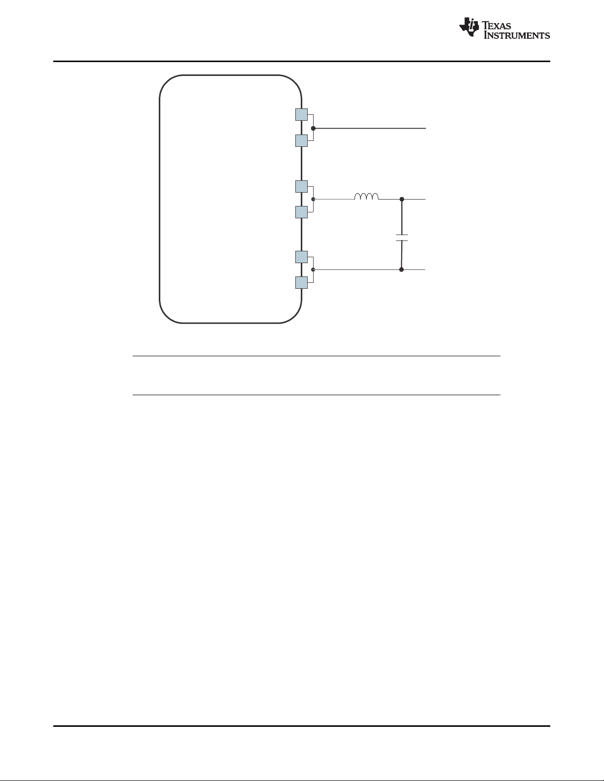
VDD2.IN(D13)
VDD2.SW(T13)
VDD2.GND(T14)
Device
VDD2.IN(P14)
VDD2.SW(R14)
VDD2.GND(R15)
032-007
L
VDD2
C
VDD2.OUT
TPS65950
SWCS032E–OCTOBER 2008–REVISED JANUARY 2011
www.ti.com
Figure 4-5. VDD2 dc-dc Application Schematic
NOTE
For the component values, see Table 15-1.
40 Power Module Copyright © 2008–2011, Texas Instruments Incorporated
Submit Documentation Feedback
Product Folder Link(s): TPS65950
TPS65950
www.ti.com
SWCS032E–OCTOBER 2008–REVISED JANUARY 2011
4.1.3 VIO dc-dc Regulator
4.1.3.1 VIO dc-dc Regulator Characteristics
The I/Os and memory dc-dc regulator is a 600-mA stepdown dc-dc converter (internal FET) with two
output voltage settings. It supplies the memories and all I/O ports in the application and is one of the first
power providers to switch on in the power-up sequence. This dc-dc regulator can be placed in sleep or
power-down mode; however, care must be taken in the sequencing of this power provider, because
numerous electrostatic discharge (ESD) blocks are connected to this supply. Table 4-5 lists the
characteristics of the regulator.
Table 4-5. VIO dc-dc Regulator Characteristics
Parameter Comments Min Typ Max Unit
Input voltage range 2.7 3.6 4.5 V
Output voltage
Output accuracy
Switching frequency 3.2 MHz
Conversion efficiency
and sleep modes
Output current
Ground current (IQ) μA
Load transient
Line transient 300 mVPPac, input rise and fall time 10 μs 10 mV
Start-up time 0.25 1 ms
Recovery time From sleep mode to on mode with constant <10 100 μs
Output shunt resistor (internal pulldown) 500 700 Ω
External coil DCR 0.1 Ω
External capacitor
(1) This voltage is tuned according to the platform and transient requirements.
(2) ±4% accuracy includes all variations (line and load regulation, line and load transient, temperature, process).
±3% accuracy is dc accuracy only.
(3) VBAT = 3.8 V, VIO = 1.8 V, Fs = 3.2 MHz, L = 1 μH, L
(4) Load transient can also be specified as 0 < IO< I
(1)
(2)
(3)
Figure 4-6 in active mode
(4)
IO= 10 mA, sleep 85%
100 mA < IO< 400 mA 85%
400 mA < IO< 600 mA 80%
On mode 700 mA
Sleep mode 10
Off at 30°C 1
Sleep, unloaded 50
Active, unloaded, not switching 300
load
Value 0.7 1 1.3 μH
Saturation current 900 mA
Value 8 10 12 μF
ESR at switching frequency 1 20 mΩ
= 100 mΩ, C = 10 μF, ESR = 10 mΩ
DCR
/2, Δt = 1 μs, 100 mV but this is not included in ±4% accuracy.
OUTmax
–4% 4%
–3% 3%
1.8
1.85
50 mV
V
Copyright © 2008–2011, Texas Instruments Incorporated Power Module 41
Submit Documentation Feedback
Product Folder Link(s): TPS65950

032-008
Outputvoltage=1.2V,VBAT =3.8V
90
80
70
60
50
40
30
20
10
00
0.0001 0.001 0.01 0.1 1
Iload(A)
Effciency(%)
100
TPS65950
SWCS032E–OCTOBER 2008–REVISED JANUARY 2011
Figure 4-6 shows the efficiency of the VIO dc-dc regulator in active and sleep modes.
www.ti.com
Figure 4-6. VIO dc-dc Regulator Efficiency in Active Mode
4.1.3.2 External Components and Application Schematic
Figure 4-7 is an application schematic with the external components of the VIO dc-dc regulator.
42 Power Module Copyright © 2008–2011, Texas Instruments Incorporated
Submit Documentation Feedback
Product Folder Link(s): TPS65950

VIO.IN(R4)
VIO.SW(R3)
VIO.GND(R2)
Device
VIO.IN(P3)
VIO.SW(T4)
VIO.GND(T3)
032-009
L
VIO
C
VIO.OUT
TPS65950
www.ti.com
SWCS032E–OCTOBER 2008–REVISED JANUARY 2011
Figure 4-7. VIO dc-dc Application Schematic
NOTE
For the component values, see Table 15-1.
Copyright © 2008–2011, Texas Instruments Incorporated Power Module 43
Submit Documentation Feedback
Product Folder Link(s): TPS65950

TPS65950
SWCS032E–OCTOBER 2008–REVISED JANUARY 2011
4.1.4 VDAC LDO Regulator
The VDAC programmable LDO regulator is a high power-supply ripple rejection (PSRR), low-noise, linear
regulator that powers the host processor dual-video DAC. It is controllable with registers through I2C and
can be powered down. Table 4-6 lists the characteristics of the regulator.
Table 4-6. VDAC LDO Regulator Characteristics
Parameter Test Conditions Min Typ Max Unit
Output Load Conditions
Filtering capacitor Connected from VDAC.OUT to analog ground 0.3 1 2.7 μF
Filtering capacitor ESR 20 600 mΩ
Electrical Characteristics
V
V
I
V
Input voltage 2.7 3.6 4.5 V
IN
Output voltage On mode 1.164 1.2 1.236 V
OUT
Rated output current On mode 70 mA
OUT
Low-power mode 5
dc load regulation On mode: 0 < IO< I
dc line regulation On mode, VIN= V
Turn-on time I
= 0, CL= 1 μF (within 10% of V
OUT
Wake-up time Full load capability 10 μs
Ripple rejection f < 20 kHz 65 dB
20 kHz < f < 100 kHz 45
f = 1 MHz 40
VIN= V
Output noise 100 Hz < f < 5 kHz 400 nV/√Hz
5 kHz < f < 400 kHz 125
400 kHz < f < 10 MHz 50
Ground current On mode, I
On mode, I
Low-power mode, I
Low-power mode, I
Off mode at 55°C 1
Dropout voltage On mode, I
DO
I
: I
Load
Transient load regulation –40 40 mV
Transient line regulation 10 mV
Min
Slew: 60 mA/μs
VINdrops 500 mV
Slew: 40 mV/μs
1.261 1.3 1.339
1.746 1.8 1.854
Max
to V
INmin
+ 1 V, IO= I
OUT
– I
OUT
OUT
OUT
Max
Max
= 0 150 μA
= I
OUTmax
= 0 15
OUT
= 1 mA 25
OUT
= I
OUTmax
INmax
at I
= I
OUT
OUTmax
) 100 μs
OUT
www.ti.com
20 mV
3 mV
350
250 mV
44 Power Module Copyright © 2008–2011, Texas Instruments Incorporated
Submit Documentation Feedback
Product Folder Link(s): TPS65950

TPS65950
www.ti.com
4.1.5 VPLL1 LDO Regulator
The VPLL1 programmable LDO regulator is high-PSRR, low-noise, linear regulator used for the host
processor phase-locked loop (PLL) supply. Table 4-7 lists the characteristics of the regulator.
Table 4-7. VPLL1 LDO Regulator Characteristics
Parameter Test Conditions Min Typ Max Unit
Output Load Conditions
Filtering capacitor Connected from VPLL1.OUT to analog ground 0.3 1 2.7 μF
Filtering capacitor ESR 20 600 mΩ
Electrical Characteristics
V
V
I
V
Input voltage 2.7 3.6 4.5 V
IN
Output voltage On mode and low-power mode 0.97 1.0 1.03 V
OUT
Rated output current On mode 40 mA
OUT
dc load regulation On mode: 0 < IO< I
dc line regulation On mode, VIN= V
Turn-on time I
Wake-up time Full load capability 10 μs
Ripple rejection f < 10 kHz 50 dB
Ground current On mode, I
Dropout voltage On mode, I
DO
Transient load regulation –40 40 mV
Transient line regulation 10 mV
SWCS032E–OCTOBER 2008–REVISED JANUARY 2011
1.164 1.2 1.236
1.261 1.3 1.339
1.746 1.8 1.854
2.716 2.8 2.884
2.91 3.0 3.090
Low-power mode 5
Max
to V
INmin
= 0, CL= 1 μF (within 10% of V
OUT
INmax
at I
= I
OUT
OUTmax
) 100 μs
OUT
20 mV
10 kHz < f < 100 kHz 40
f = 1 MHz 30
VIN= V
On mode, I
Low-power mode, I
Low-power mode, I
+ 1 V, IO= I
OUT
OUT
OUT
Max
= 0 70 μA
= I
OUTmax
= 0 15
OUT
= 1 mA 16
OUT
110
Off mode at 55°C 1
OUT
I
: I
Min
– I
Max
Load
Slew: 60 mA/μs
= I
OUTmax
250 mV
VINdrops 500 mV
Slew: 40 mV/μs
3 mV
Copyright © 2008–2011, Texas Instruments Incorporated Power Module 45
Submit Documentation Feedback
Product Folder Link(s): TPS65950

TPS65950
SWCS032E–OCTOBER 2008–REVISED JANUARY 2011
4.1.6 VPLL2 LDO Regulator
The VPLL2 programmable LDO regulator is a high-PSRR, low-noise, linear regulator used for the host
processor PLL supply. Table 4-8 lists the characteristics of the regulator.
Table 4-8. VPLL2 LDO Regulator Characteristics
Parameter Test Conditions Min Typ Max Unit
Output Load Conditions
Filtering capacitor Connected from VPLL2.OUT to analog ground 0.3 1 2.7 μF
Filtering capacitor ESR 20 600 mΩ
Electrical Characteristics
V
V
I
V
Input voltage 2.7 3.6 4.5 V
IN
Output voltage On mode and low-power mode 1.795 1.85 1.906 V
OUT
Rated output current mA
OUT
On mode 100
Low-power mode 5
dc load regulation On mode: 0 < IO< I
dc line regulation On mode, VIN= V
Turn-on time I
= 0, CL= 1 μF (within 10% of V
OUT
Wake-up time Full load capability 10 μs
f < 10 kHz 50
Ripple rejection dB
10 kHz < f < 100 kHz 40
f = 1 MHz 30
VIN= V
On mode, I
On mode, I
Ground current Low-power mode, I
Low-power mode, I
Off mode at 55°C 1
Dropout voltage On mode, I
DO
I
: I
Load
Transient load regulation –40 40 mV
Transient line regulation 10 mV
Min
Slew: 40 mA/μs
VINdrops 500 mV
Slew: 40 mV/μs
0.672 0.7 0.728
0.97 1.0 1.03
1.164 1.2 1.236
1.261 1.3 1.339
1.455 1.5 1.545
1.746 1.8 1.854
2.425 2.5 2.575
2.522 2.6 2.678
2.716 2.8 2.884
2.765 2.85 2.936
2.91 3.0 3.09
3.05 3.15 3.245
Max
to V
INmin
+ 1 V, IO= I
OUT
– I
OUT
OUT
OUT
Max
Max
= 0 70
= I
OUTmax
= 0 17 μA
OUT
= 1 mA 20
OUT
= I
OUTmax
INmax
at I
= I
OUT
OUTmax
) 100 μs
OUT
www.ti.com
20 mV
3 mV
160
250 mV
46 Power Module Copyright © 2008–2011, Texas Instruments Incorporated
Submit Documentation Feedback
Product Folder Link(s): TPS65950

TPS65950
www.ti.com
4.1.7 VMMC1 LDO Regulator
The VMMC1 LDO regulator is a programmable linear voltage converter that powers the multimedia
channel (MMC) slot. It includes a discharge resistor and overcurrent (short -ircuit) protection. This LDO
regulator can also be turned off automatically when MMC card extraction is detected. The VMMC1 LDO
can be powered through an independent supply other than the battery; for example, a charge pump (CP).
In this case, the input from the VMMC1 LDO can be higher than the battery voltage. Table 4-9 lists the
characteristics of the regulator.
Table 4-9. VMMC1 LDO Regulator Characteristics
Parameter Test Conditions Min Typ Max Unit
Output Load Conditions
Filtering capacitor Connected from VMMC1.OUT to analog ground 0.3 1 2.7 μF
Filtering capacitor ESR 20 600 mΩ
Electrical Characteristics
V
V
I
V
Input voltage 2.7 3.6 5.5 V
IN
Output voltage On mode and low-power mode V
OUT
Rated output current mA
OUT
dc load regulation On mode: 0 < IO< I
dc line regulation On mode, VIN= V
Turn-on time I
Wake-up time Full load capability 10 μs
Ripple rejection dB
Ground current Low-power mode, I
Dropout voltage On mode, I
DO
Transient load regulation –40 40 mV
Transient line regulation 10 mV
SWCS032E–OCTOBER 2008–REVISED JANUARY 2011
1.7945 1.85 1.9055
2.7645 2.85 2.9355
2.91 3.0 3.09
3.0555 3.15 3.2445
On mode 220
Low-power mode 5
Max
to V
INmin
= 0, CL= 1 μF (within 10% of V
OUT
INmax
at I
= I
OUT
OUTmax
) 100 μs
OUT
20 mV
f < 10 kHz 50
10 kHz < f < 100 kHz 40
f = 1 MHz 25
VIN= V
On mode, I
On mode, I
Low-power mode, I
Off mode at 55°C 1
I
Load
Slew: 40 mA/μs
: I
Min
+ 1 V, IO= I
OUT
– I
OUT
OUT
OUT
Max
Max
= 0 70
= I
OUTmax
= 0 17 μA
OUT
= 5 mA 20
OUT
= I
OUTmax
290
250 mV
VINdrops 500 mV
Slew: 40 mV/μs
3 mV
Copyright © 2008–2011, Texas Instruments Incorporated Power Module 47
Submit Documentation Feedback
Product Folder Link(s): TPS65950

TPS65950
SWCS032E–OCTOBER 2008–REVISED JANUARY 2011
4.1.8 VMMC2 LDO Regulator
The VMMC2 LDO regulator is a programmable linear voltage converter that powers MMC slot 2. It
includes a discharge resistor and overcurrent (short-circuit) protection. The VMMC2 LDO can be powered
through an independent supply other than the battery (for example, a CP). In this case, the input from the
VMMC2 LDO can be higher than the battery voltage. Table 4-10 lists the characteristics of the regulator.
Table 4-10. VMMC2 LDO Regulator Characteristics
Parameter Test Conditions Min Typ Max Unit
Output Load Conditions
Filtering capacitor Connected from VMMC2.OUT to analog ground 0.3 1 2.7 μF
Filtering capacitor ESR 20 600 mΩ
Electrical Characteristics
V
V
I
V
Input voltage 2.7 3.6 5.5 V
IN
Output voltage On mode and low-power mode V
OUT
Rated output current mA
OUT
On mode 100
Low-power mode 5
dc load regulation On mode: 0 < IO< I
dc line regulation On mode, VIN= V
Turn-on time I
= 0, CL= 1 μF (within 10% of V
OUT
Wake-up time Full load capability 10 μs
f < 10 kHz 50
Ripple rejection dB
10 kHz < f < 100 kHz 40
f = 1 MHz 30
VIN= V
On mode, I
On mode, I
Ground current Low-power mode, I
Low-power mode, I
Off mode at 55°C 1
Dropout voltage On mode, I
DO
I
: I
Load
Transient load regulation –40 40 mV
Transient line regulation 10 mV
Min
Slew: 40 mA/μs
VINdrops 500 mV
Slew: 40 mV/μs
0.7 1.0 1.03
1.164 1.2 1.236
1.261 1.3 1.339
1.455 1.5 1.545
1.746 1.8 1.854
1.795 1.85 1.906
2.425 2.5 2.575
2.522 2.6 2.678
2.716 2.8 2.884
2.765 2.85 2.936
2.91 3.0 3.09
3.056 3.15 3.245
Max
to V
INmin
+ 1 V, IO= I
OUT
– I
OUT
OUT
OUT
Max
Max
= 0 70
= I
OUTmax
= 0 17 μA
OUT
= 50 μA 20
OUT
= I
OUTmax
INmax
at I
= I
OUT
OUTmax
) 100 μs
OUT
www.ti.com
20 mV
3 mV
170
250 mV
48 Power Module Copyright © 2008–2011, Texas Instruments Incorporated
Submit Documentation Feedback
Product Folder Link(s): TPS65950

TPS65950
www.ti.com
4.1.9 VSIM LDO Regulator
The VSIM voltage regulator is a programmable, low-dropout, linear voltage regulator that supplies the
subscriber identity module (SIM)-card and the SIM-card driver. This LDO regulator can be turned off
automatically when SIM card extraction is detected. Table 4-11 lists the characteristics of the regulator.
Parameter Test Conditions Min Typ Max Unit
Output Load Conditions
Filtering capacitor Connected from VSIM.OUT to analog ground 0.3 1 2.7 μF
Filtering capacitor ESR 20 600 mΩ
Electrical Characteristics
V
V
I
V
Input voltage 2.7 3.6 4.5 V
IN
Output voltage On mode and low-power mode V
OUT
Rated output current mA
OUT
dc load regulation On mode: 0 < IO< I
dc line regulation On mode, VIN= V
Turn-on time I
Wake-up time Full load capability 10 μs
Ripple rejection dB
Ground current Low-power mode, I
Dropout voltage On mode, I
DO
Transient load regulation –40 40 mV
Transient line regulation 10 mV
SWCS032E–OCTOBER 2008–REVISED JANUARY 2011
Table 4-11. VSIM LDO Regulator Characteristics
0.97 1.0 1.03
1.164 1.2 1.236
1.261 1.3 1.339
1.746 1.8 1.854
2.716 2.8 2.884
2.91 3.0 3.09
On mode 50
Low-power mode 1
Max
to V
INmin
= 0, CL= 1 μF (within 10% of V
OUT
f < 10 kHz 50
10 kHz < f < 100 kHz 40
f = 1 MHz 30
VIN= V
On mode, I
On mode, I
Low-power mode, I
Off mode at 55°C 1
I
Load
Slew: 40 mA/μs
: I
Min
+ 1 V, IO= I
OUT
– I
OUT
OUT
OUT
Max
Max
= 0 70
= I
OUTmax
= 0 15 μA
OUT
= 1 mA 16
OUT
= I
OUTmax
VINdrops 500 mV
Slew: 40 mV/μs
INmax
at I
= I
OUT
OUTmax
) 100 μs
OUT
20 mV
3 mV
120
250 mV
Copyright © 2008–2011, Texas Instruments Incorporated Power Module 49
Submit Documentation Feedback
Product Folder Link(s): TPS65950

TPS65950
SWCS032E–OCTOBER 2008–REVISED JANUARY 2011
4.1.10 VAUX1 LDO Regulator
The VAUX1 GP LDO regulator powers the auxiliary devices. The VAUX1 regulator can also support an
inductive load such as a vibrator. While operating in vibrator mode, the VAUX1 LDO has the following
features:
• Programmable, register-controlled, soft-start function
• Enabled through the VIBRA.SYNC pin
• Programmable, register-controlled, duty cycle (PWM generator) based on a nominal 4-Hz cycle derived
from an internal 32-kHz clock
Table 4-12 lists the characteristics of the regulator.
Table 4-12. VAUX1 LDO Regulator Characteristics
Parameter Test Conditions Min Typ Max Unit
Output Load Conditions
Filtering capacitor Connected from VAUX1.OUT to analog ground 0.3 1 2.7 μF
Filtering capacitor ESR 20 600 mΩ
Vibrator inductive load
Vibrator load resistance
Electrical Characteristics
V
V
I
Input voltage 2.7 3.6 4.5 V
IN
Output voltage On mode and low-power mode 2.425 2.5 2.575 V
OUT
Rated output current mA
OUT
dc load regulation On mode: I
dc line regulation On mode, VIN= V
Turn-on time μs
Turn-off time 5000 μs
Wake-up time Full load capability 10 μs
Ripple rejection dB
Ground current Low-power mode, I
V
Dropout voltage On mode, I
DO
Transient load regulation –40 40 mV
Transient line regulation 10 mV
(1) Parameter not tested, used for design specification only
(1)
(1)
Connected from VAUX1.OUT to analog ground 70 700 μH
On mode 200
Low-power mode 5
= I
OUT
I
= 0, CL= 1 μF (within 10% of V
OUT
Soft-start function for inductive load 500
f < 10 kHz 50
10 kHz < f < 100 kHz 40
f = 1 MHz 25
VIN= V
On mode, I
On mode, I
+ 1 V, IO= I
OUT
= 0 70
OUT
= I
OUT
Low-power mode, I
Off mode at 55°C 1
= I
OUT
I
: I
Min
– I
Max
Load
Slew: 40 mA/μs
VINdrops 500 mV
Slew: 40 mV/μs
15 50 Ω
1.455 1.5 1.545
1.746 1.8 1.854
2.716 2.8 2.884
2.91 3.0 3.09
to 0 20 mV
OUTmax
to V
INmin
Max
OUTmax
= 0 15 μA
OUT
= 5 mA 20
OUT
OUTmax
INmax
at I
= I
OUT
OUTmax
) 100
OUT
www.ti.com
3 mV
270
250 mV
50 Power Module Copyright © 2008–2011, Texas Instruments Incorporated
Submit Documentation Feedback
Product Folder Link(s): TPS65950

TPS65950
www.ti.com
4.1.11 VAUX2 LDO Regulator
The VAUX2 GP LDO regulator powers the auxiliary devices. Table 4-13 lists the characteristics of the
regulator.
Table 4-13. VAUX2 LDO Regulator Characteristics
Parameter Test Conditions Min Typ Max Unit
Output Load Conditions
Filtering capacitor Connected from VAUX2.OUT to analog ground 0.3 1 2.7 μF
Filtering capacitor ESR 20 600 mΩ
Electrical Characteristics
V
V
I
V
Input voltage 2.7 3.6 4.5 V
IN
Output voltage On mode and low-power mode –3% 3% V
OUT
Rated output current mA
OUT
On mode 100
Low-power mode 5
dc load regulation On mode: I
dc line regulation On mode, VIN= V
Turn-on time I
Wake-up time Full load capability 10 μs
f < 10 kHz 50
Ripple rejection dB
10 kHz < f < 100 kHz 40
f = 1 MHz 25
VIN= V
On mode, I
On mode, I
Ground current Low-power mode, I
Low-power mode, I
Off mode at 55°C 1
Dropout voltage On mode, I
DO
Transient load regulation –40 40 mV
Transient line regulation 10 mV
I
Slew: 40 mA/μs
VINdrops 500 mV
Slew: 40 mV/μs
= I
OUT
= 0, CL= 1 μF (within 10% of V
OUT
+ 1 V, IO= I
OUT
= 0 70
OUT
= I
OUT
= I
OUT
: I
Min
– I
Max
Load
to 0 20 mV
OUTmax
to V
INmin
Max
OUTmax
= 0 17 μA
OUT
= 5 mA 20
OUT
OUTmax
INmax
SWCS032E–OCTOBER 2008–REVISED JANUARY 2011
1.3
1.5
1.7
1.8
1.9
2.0
2.1
2.2
2.3
2.4
2.5
2.8
at I
= I
OUT
OUTmax
) 100 μs
OUT
3 mV
170
250 mV
Copyright © 2008–2011, Texas Instruments Incorporated Power Module 51
Submit Documentation Feedback
Product Folder Link(s): TPS65950
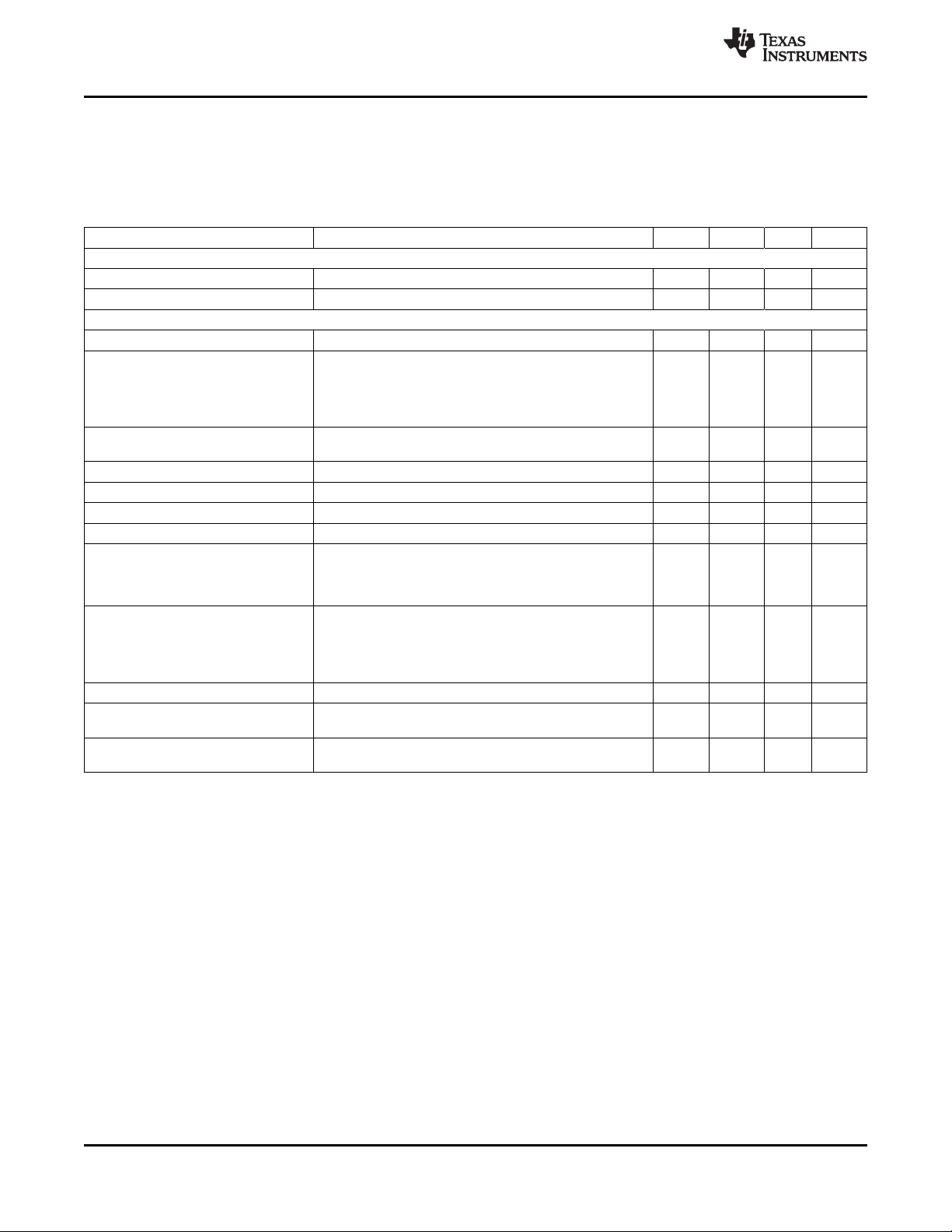
TPS65950
SWCS032E–OCTOBER 2008–REVISED JANUARY 2011
4.1.12 VAUX3 LDO Regulator
The VAUX3 GP LDO regulator powers the auxiliary devices. Table 4-14 lists the characteristics of the
regulator.
Table 4-14. VAUX3 LDO Regulator Characteristics
Parameter Test Conditions Min Typ Max Unit
Output Load Conditions
Filtering capacitor Connected from VAUX3.OUT to analog ground 0.3 1 2.7 μF
Filtering capacitor ESR 20 600 mΩ
Electrical Characteristics
V
V
I
V
Input voltage 2.7 3.6 4.5 V
IN
Output voltage On mode and low-power mode 2.425 2.5 2.575 V
OUT
Rated output current mA
OUT
On mode 200
Low-power mode 5
dc load regulation On mode: I
dc line regulation On mode, VIN= V
Turn-on time I
= 0, CL= 1 μF (within 10% of V
OUT
Wake-up time Full load capability 10 μs
f < 10 kHz 50
Ripple rejection dB
10 kHz < f < 100 kHz 40
f = 1 MHz 25
VIN= V
On mode, I
On mode, I
Ground current Low-power mode, I
Low-power mode, I
Off mode at 55°C 1
Dropout voltage On mode, I
DO
I
: I
Load
Transient load regulation –40 40 mV
Transient line regulation 10 mV
Min
Slew: 40 mA/μs
VINdrops 500 mV
Slew: 40 mV/μs
1.455 1.5 1.545
1.746 1.8 1.854
2.716 2.8 2.884
2.91 3.0 3.09
= I
OUT
+ 1 V, IO= I
OUT
= 0 70
OUT
= I
OUT
= I
OUT
– I
Max
to 0 20 mV
OUTmax
to V
INmin
Max
OUTmax
= 0 15 μA
OUT
= 5 mA 20
OUT
OUTmax
INmax
at I
= I
OUT
OUTmax
) 100 μs
OUT
www.ti.com
3 mV
270
250 mV
52 Power Module Copyright © 2008–2011, Texas Instruments Incorporated
Submit Documentation Feedback
Product Folder Link(s): TPS65950
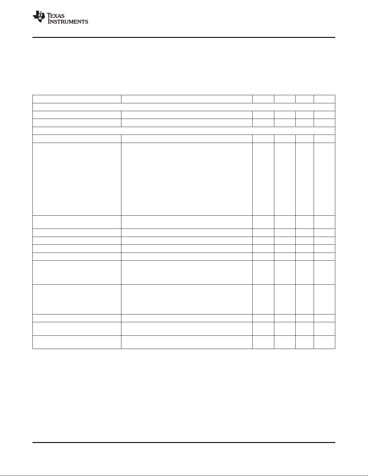
TPS65950
www.ti.com
4.1.13 VAUX4 LDO Regulator
The VAUX4 GP LDO regulator powers the auxiliary devices. The VAUX4 regulator has an independent
supply input pin and can be preregulated by an external voltage. Table 4-15 lists the characteristics of the
regulator.
Table 4-15. VAUX4 LDO Regulator Characteristics
Parameter Test Conditions Min Typ Max Unit
Output Load Conditions
Filtering capacitor Connected from VAUX4.OUT to analog ground 0.3 1 2.7 μF
Filtering capacitor ESR 20 600 mΩ
Electrical Characteristics
V
V
I
V
Input voltage 2.7 3.6 4.5 V
IN
Output voltage On mode and low-power mode 1.795 1.85 1.906 V
OUT
Rated output current mA
OUT
On mode 100
Low-power mode 5
dc load regulation On mode: I
dc line regulation On mode, VIN= V
Turn-on time I
Wake-up time Full load capability 10 μs
f < 10 kHz 50
Ripple rejection dB
10 kHz < f < 100 kHz 40
f = 1 MHz 30
VIN= V
On mode, I
On mode, I
Ground current Low-power mode, I
Low-power mode, I
Off mode at 55°C 1
Dropout voltage On mode, I
DO
Transient load regulation –40 40 mV
Transient line regulation 10 mV
I
Slew: 40 mA/μs
VINdrops 500 mV
Slew: 40 mV/μs
= I
OUT
= 0, CL= 1 μF (within 10% of V
OUT
+ 1 V, IO= I
OUT
= 0 70
OUT
= I
OUT
= I
OUT
: I
Min
– I
Max
Load
to 0 20 mV
OUTmax
to V
INmin
Max
OUTmax
= 0 17 μA
OUT
= 5 mA 20
OUT
OUTmax
INmax
SWCS032E–OCTOBER 2008–REVISED JANUARY 2011
0.672 0.7 0.728
0.97 1.0 1.03
1.164 1.2 1.236
1.261 1.3 1.339
1.455 1.5 1.545
1.746 1.8 1.854
2.425 2.5 2.575
2.522 2.6 2.678
2.716 2.8 2.884
2.765 2.85 2.936
2.91 3.0 3.09
3.056 3.15 3.245
at I
= I
OUT
OUTmax
) 100 μs
OUT
3 mV
170
250 mV
Copyright © 2008–2011, Texas Instruments Incorporated Power Module 53
Submit Documentation Feedback
Product Folder Link(s): TPS65950

TPS65950
SWCS032E–OCTOBER 2008–REVISED JANUARY 2011
www.ti.com
4.1.14 Internal LDOs
Table 4-16 lists the regulators that power the device, and the output loads associated with them.
Table 4-16. Output Load Conditions
Regulator Parameter Test Conditions Min Typ Max Unit
VINTDIG LDO Filtering capacitor Connected from VINTDIG.OUT to analog 0.3 1 2.7 μF
Filtering capacitor ESR 20 600 mΩ
VINTANA1 LDO Filtering capacitor Connected from VINTANA1.OUT to analog 0.3 1 2.7 μF
Filtering capacitor ESR 20 600 mΩ
VINTANA2 LDO Filtering capacitor Connected from VINTANA2.OUT to analog 0.3 1 2.7 μF
Filtering capacitor ESR 20 600 mΩ
VRUSB_3V1 LDO Filtering capacitor Connected from VUSB.3P1 to GND 0.3 1 2.7 μF
Filtering capacitor ESR 0 10 600 mΩ
VRUSB_1V8 LDO Filtering capacitor Connected from VINTUSB1P8.OUT to GND 0.3 1 2.7 μF
Filtering capacitor ESR 0 10 600 mΩ
VRUSB_1V5 LDO Filtering capacitor Connected from VINTUSB1P5 to GND 0.3 1 2.7 μF
Filtering capacitor ESR 0 10 600 mΩ
ground
ground
ground
4.1.15 CP
The CP generates a 4.8-V (nominal) power supply voltage from the battery to the VBUS pin. The input
voltage range is 2.7 to 4.5 V for the battery voltage. The CP operating frequency is 1 MHz.
The CP tolerates 7 V on VBUS when it is in power-down mode. The CP integrates a short-circuit current
limitation at 450 mA. Table 4-17 lists the characteristics of the CP.
Parameter Test Conditions Min Typ Max Unit
Output Load Conditions
Filtering capacitor Connected from VBUS to VSSP 1.41 4.7 6.5 μF
Flying capacitor Connected from CP to CN 1.32 2.2 3.08 μF
Filtering capacitor ESR 20 mΩ
Electrical Characteristics
V
V
I
Input voltage On mode: VIN= VBAT 2.7 3.6 4.5 V
IN
Output voltage 4.6 4.8 5.25 V
O
Rated output current mA
load
Efficiency I
Setting time I
Startup time 3 ms
Short-circuit limitation current 250 350 450 mA
dc load regulation I
dc line regulation 250 350 mV
Transient load regulation mV
Transient line regulation VBAT
Table 4-17. CP Characteristics
VBAT > 3 V at VBUS 0 100
2.7 V < VBAT < 3 V, at VBUS 0 50
= 100 mA, VBAT = 3.6 V 55%
Load
LOADmax/2
LOADmin
to I
to I
LOADmax
3.0 V to VBAT
I
= 100 mA
Load
I
VBUS_5Vmax/2
50 μs, C = 2*4.7 μF
0 – I
VBUS_5Vmax/2
to VBAT
min
in 5 μs 100 400 μs
LOAmax
250 500 mV
max
– I
VBUS_5Vmax
300 350
, 50 μs, C = 2*4.7 μF 350
in 50 μs, C = 2*4.7 μF 300 350 mV
max
54 Power Module Copyright © 2008–2011, Texas Instruments Incorporated
Submit Documentation Feedback
Product Folder Link(s): TPS65950

TPS65950
www.ti.com
4.1.16 USB LDO Short-Circuit Protection Scheme
The short-circuit current for the LDOs and dc-dc converters in TPS65950 is approximately twice the
maximum load current. In certain cases when the output of the block is shorted to ground, the power
dissipation can exceed the 1.2-W requirement if no action is taken. A short-circuit protection scheme is
included in the TPS65950 to ensure that if the output of an LDO or dc-dc is short-circuited, the power
dissipation does not exceed the 1.2-W level.
The three USB LDOs, VRUSB3V1, VRUSB1V8, and VRUSB1V5, are included in this short-circuit
protection scheme, which monitors the LDO output voltage at a frequency of 1 Hz and generates an
interrupt (sc_it) when a short circuit is detected.
The scheme compares the LDO output voltage to a reference voltage and detects a short circuit if the
LDO voltage drops below this reference value (0.5 or 0.75 V programmable). In the case of the
VRUSB3V1 and VRUSB1V8 LDOs, the reference is compared with a divided-down voltage (1.5 V typical).
If a short circuit is detected on VRUSB3V1, the power subchip FSM switches this LDO to sleep mode.
If a short circuit is detected on VRUSB1V8 or VRUSB1V5, the power subchip FSM switches off the
relevant LDO.
4.2 Power References
The bandgap voltage reference is filtered (resistance/capacitance [RC] filter) using an external capacitor
connected across the VREF output and an analog ground (REFGND). The VREF voltage is scaled,
distributed, and buffered in the device. The bandgap is started in fast mode (not filtered), and is set
automatically by the D machine in slow mode (filtered, less noisy) when required.
SWCS032E–OCTOBER 2008–REVISED JANUARY 2011
Table 4-18 lists the characteristics of the voltage references.
Table 4-18. Voltage Reference Characteristics
Parameter Test Conditions Min Typ Max Unit
Output Load Condition
Filtering capacitor Connected from V
Electrical Characteristics
VINInput voltage On mode 2.7 3.6 4.5 V
Internal bandgap reference voltage On mode, measured through TESTV terminal 1.272 1.285 1.298 V
Reference voltage (V
Retention mode reference On mode 0.492 0.5 0.508 V
I
NMOS sink 0.9 1 1.1 µA
REF
Ground current Bandgap 25 µA
Output spot noise 100 Hz 1 µV/√Hz
A-weighted noise (rms) 200 nV (ms)
P-weighted noise (rms) 150 nV (ms)
Integrated noise 20 Hz to 100 kHz 2.2 µV
I
trim bit LSB 0.1 µA
BIAS
Ripple rejection < 1 MHz from VBAT 60 dB
Start-up time 1 ms
terminal) On mode 0.725 0.75 0.7575 V
REF
IREF block 20
Preregulator 15
VREF buffer 10
Retention reference buffer 10
to REFGND 0.3 1 2.7 μF
REF
Copyright © 2008–2011, Texas Instruments Incorporated Power Module 55
Submit Documentation Feedback
Product Folder Link(s): TPS65950

TPS65950
SWCS032E–OCTOBER 2008–REVISED JANUARY 2011
www.ti.com
4.3 Power Control
4.3.1 Backup Battery Charger
If the backup battery is rechargeable, it can be recharged from the main battery. A programmable voltage
regulator powered by the main battery allows recharging of the backup battery. The backup battery charge
must be enabled using a control bit register. Recharging starts when two conditions are met:
• Main battery voltage > backup battery voltage
• Main battery > 3.2 V
The comparators of the backup battery system (BBS) give the two thresholds of the backup battery charge
startup. The programmed voltage for the charger gives the end-of-charge threshold. The programmed
current for the charger gives the charge current.
Overcharging is prevented by measurement of the backup battery voltage through the GP ADC.
Table 4-19 lists the characteristics of the backup battery charger.
Table 4-19. Backup Battery Charger Characteristics
Parameter Test Conditions Min Typ Max Unit
VBACKUP-to-MADC input attenuation VBACKUP from 1.8 to 3.3 V 0.33 V/V
Backup battery charging current VBACKUP = 2.8 V, BBCHEN = 1, BBISEL = 00 10 25 45 μA
VBACKUP = 2.8 V, BBCHEN = 1, BBISEL = 01 105 150 270 μA
VBACKUP = 2.8 V, BBCHEN = 1, BBISEL = 10 350 500 900 μA
VBACKUP = 2.8 V, BBCHEN = 1, BBISEL = 11 0.7 1 1.8 mA
VBACKUP = 0 V, BBCHEN = 1, BBISEL = 00 17.5 25 45 μA
VBACKUP = 0 V, BBCHEN = 1, BBISEL = 01 105 150 270 μA
VBACKUP = 0 V, BBCHEN = 1, BBISEL = 10 350 500 900 μA
VBACKUP = 0 V, BBCHEN = 1, BBISEL = 11 0.7 1 1.8 mA
End backup battery charging voltage: I
VBBCHGEND
VBACKUP
I
VBACKUP
I
VBACKUP
I
VBACKUP
= –10 μA, BBSEL = 00 2.4 2.5 2.6 V
= –10 μA, BBSEL = 01 2.9 3.0 3.1 V
= –10 μA, BBSEL = 10 3.0 3.1 3.2 V
= –10 μA, BBSEL = 11 3.1 3.2 3.3 V
4.3.2 Battery Monitoring and Threshold Detection
4.3.2.1 Power On/Power Off and Backup Conditions
Table 4-20 lists the threshold levels of the battery.
Table 4-20. Battery Threshold Levels
Parameter Test Conditions Min Typ Max Unit
Main battery charged threshold Measured on VBAT terminal 3.1 3.2 3.3 V
VMBCH
Main battery low threshold VMBLO VBACKUP = 3.2 V, measured on VBAT terminal (monitored 2.55 2.7 2.85 V
Main battery high threshold VMBHI Measured on terminal VBAT, VBACKUP = 0 V 2.5 2.65 2.95 V
Batteries not present threshold VBNPR Measured on terminal VBACKUP with VBAT < 2.1 V 1.6 1.8 2.0 V
56 Power Module Copyright © 2008–2011, Texas Instruments Incorporated
on terminal ONNOFF)
Measured on terminal VBAT, VBACKUP = 3.2 V 2.5 2.85 2.95
Measured on terminal VBAT with VBACKUP = 0 V 1.95 2.1 2.25
(monitored on terminal VRRTC)
Submit Documentation Feedback
Product Folder Link(s): TPS65950
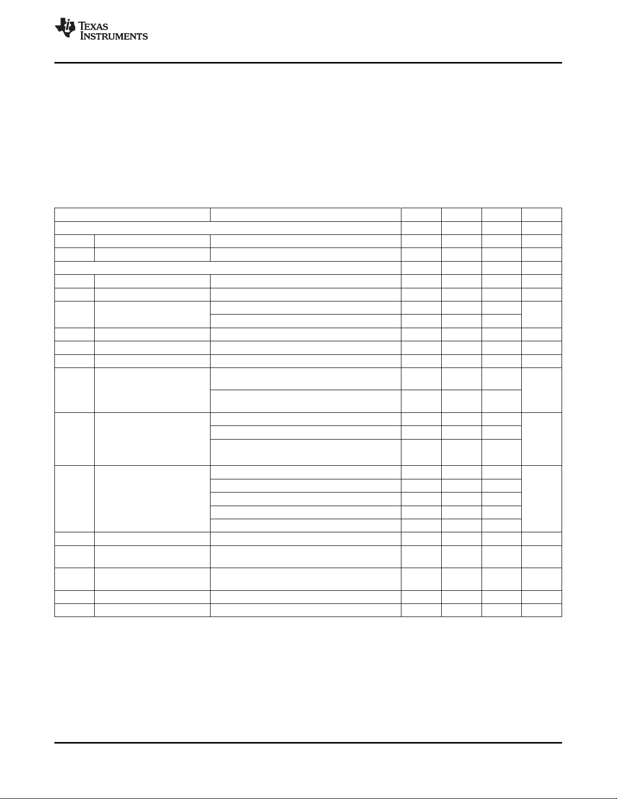
TPS65950
www.ti.com
4.3.3 VRRTC LDO Regulator
The VRRTC voltage regulator is a programmable, low dropout, linear voltage regulator supplying (1.5 V)
the embedded real-time clock (32.768-kHz oscillator) and dedicated I/Os of the digital host counterpart.
The VRRTC regulator is also the supply voltage of the power-management digital state-machine. The
VRRTC regulator is supplied from the UPR line, switched on by the main or backup battery, depending on
the system state. The VRRTC output is present as long as a valid energy source is present. The VRRTC
line is supplied by an LDO when VBAT > 2.7, and a clamp circuit when in backup mode. Table 4-21
describes the regulator characteristics.
Table 4-21. VRRTC LDO Regulator Characteristics
Parameter Test Conditions Min Typ Max Unit
Output Load Conditions
Filtering capacitor Connected from VRTC.OUT to analog ground 0.3 1 2.7 μF
Filtering capacitor ESR 20 600 mΩ
Electrical Characteristics
V
IN
V
OUT
I
OUT
V
DO
(1) For nominal output voltage
Input voltage On mode 2.7 VBAT 4.5 V
Output voltage On mode 1.45 1.5 1.55 V
Rated output current On mode 30 mA
DC load regulation On mode: I
DC line regulation On mode, VIN= V
Turn-on time I
Wake-up time On mode from low power to On mode, I
Ripple rejection (VRRTC) f < 10 kHz 50 dB
Ground current On mode, I
Dropout voltage
(1)
Transient load regulation I
Transient line regulation VINdrops 500 mV 10 mV
Overshoot Softstart 3%
Pull down resistance Default in off mode 250 320 450 Ω
SWCS032E–OCTOBER 2008–REVISED JANUARY 2011
Sleep mode 1
= I
OUT
= 0, at V
OUT
V
OUT
= V
OUT
OUTfinal
± 3%
From backup to On mode, I
V
OUTfinal
± 3%
to 0 100 mV
OUTmax
INmin
= V
to V
OUTfinal
at I
INmax
OUT
= I
OUTmax
± 3% 100 μs
= 0, at 100 μs
OUT
OUT
= 0, at V
= 100
OUT
100 mV
10 kHz < f < 100 kHz 40
f = 1 MHz 30
VIN= V
On mode, I
Sleep mode, I
Sleep mode, I
+ 1 V, IO= I
OUT
OUT
OUT
OUT
OUT
MAX
= 0 70 μA
= I
OUTmax
= 0 10
= 1 mA 11
100
Off mode 1
On mode, I
: I
LOAD
Slew: 40 mA/μs
MIN
OUT
– I
MAX
= I
OUTmax
250 mV
–40 40 mV
Slew: 40 mV/μs
Copyright © 2008–2011, Texas Instruments Incorporated Power Module 57
Submit Documentation Feedback
Product Folder Link(s): TPS65950

TPS65950
SWCS032E–OCTOBER 2008–REVISED JANUARY 2011
www.ti.com
4.4 Power Consumption
Table 4-22 describes the power consumption, depending on the use cases.
NOTE
Typical power consumption is obtained in nominal operating conditions with the TPS65950 in
stand-alone mode.
Table 4-22. Power Consumption
Mode Description Typical Consumption
Backup backup domain. No main source is connected. Consumption is on the VBAT not present 2.25 * 3.2 = 7.2 μW
Wait-on VBAT = 3.8 V 64 * 3.8 = 243.2 μW
Active No Load enabled with full current capability, internal reset is released, and the VBAT = 3.8 V 3291 * 3.8 = 12505 μW
Sleep No Load enabled but in low-consumption mode, and the associated processor is VBAT = 3.8 V 496 * 3.8 = 1884.4 μW
Only the RTC date is maintained with a couple of registers in the
backup battery.
The phone is apparently off for the user, a main battery is present and
well-charged. The RTC registers (registers in the backup domain) are
maintained. Wake-up capabilities (like the PWRON button) are
available.
The subsystem is powered by the main battery, all supplies are
associated processor is running.
The main battery powers the subsystem, selected supplies are
in low-power mode.
Table 4-23 lists the regulator states for each mode.
Table 4-23. Regulator States Depending on Use Cases
Regulator
VAUX1 OFF OFF OFF OFF
VAUX2 OFF OFF SLEEP ON
VAUX3 OFF OFF OFF OFF
VAUX4 OFF OFF SLEEP ON
VMMC1 OFF OFF OFF OFF
VMMC2 OFF OFF SLEEP ON
VPLL1 OFF OFF SLEEP ON
VPLL2 OFF OFF SLEEP ON
VSIM OFF OFF OFF OFF
VDAC OFF OFF OFF OFF
VINTANA1 OFF OFF SLEEP ON
VINTANA2 OFF OFF SLEEP ON
VINTDIG OFF OFF SLEEP ON
VIO OFF OFF SLEEP ON
VDD1 OFF OFF SLEEP ON
VDD2 OFF OFF SLEEP ON
VUSB_1V5 OFF OFF OFF OFF
VUSB_1V8 OFF OFF OFF OFF
VUSB_3V1 OFF OFF SLEEP SLEEP
Backup Wait-On Sleep No Load Active No Load
Mode
58 Power Module Copyright © 2008–2011, Texas Instruments Incorporated
Submit Documentation Feedback
Product Folder Link(s): TPS65950

TPS65950
www.ti.com
4.5 Power Management
4.5.1 Boot Modes
The modes corresponding to the BOOT0–BOOT1 combination value are listed in Table 4-24.
Name Description BOOT0 BOOT1
MC027 Master_C027_Generic 01 0 1
MC021 Master_C021_Generic 10 1 0
SC021 Slave_C021_Generic 11 1 1
4.5.2 Process Modes
The process modes parameter defines:
• The boot voltage for the host core
• The boot sequence associated with the process
• The dynamic voltage and frequency scaling (DVFS) protocol associated with the process
4.5.2.1 C027.0 Mode
SWCS032E–OCTOBER 2008–REVISED JANUARY 2011
Table 4-24. BOOT Mode Description
Reserved 0 0
Table 4-25 lists the parameters for C027.0 mode.
Table 4-25. C027.0 Mode Description
Boot core voltage 1.3 V
Power sequence VIO followed by VDD1 and VPLL
DVFS protocol VMODE1/2
4.5.2.2 C021.M Mode
Table 4-26 lists the parameters for C021.M mode.
Table 4-26. C021.M Mode Description
Boot core voltage 1.2 V
Power sequence VIO followed by VPLL1, VDD2, VDD1
DVFS protocol SmartReflex IF (I2C high speed)
4.5.3 Power-On Sequence
4.5.3.1 Timings Before Sequence_Start
The starting time of the power-on sequence relative to external events is shown in Figure 4-8.
Copyright © 2008–2011, Texas Instruments Incorporated Power Module 59
Submit Documentation Feedback
Product Folder Link(s): TPS65950

Vbkup
User_Action
Vbat
Sequence_Start
VAC
Sequence_Start
PWRON
Sequence_Start
PWRON
Sequence_Start
Pushbuttondebouncing-30ms
0 ms
Starting_Eventismainbatteryinsertion
Starting_EventisPWRONbutton
Starting_Eventischargerinsertion
Starting_EventisPWRONrisingwhendeviceisinslavemode
61 ms-2cycle32k
61 ms-2cycle32k
Vbus
Sequence_Start
Starting_EventisVBUSinsertion
61 ms-2cycle32k
032-010
TPS65950
SWCS032E–OCTOBER 2008–REVISED JANUARY 2011
www.ti.com
Figure 4-8. Timings Before Sequence Start
4.5.3.2 OMAP2 Power-On Sequence
Figure 4-9 shows the timing and control that must occur in Master_C027_Generic mode. Sequence_Start
occurs according to the events shown in Figure 4-8.
60 Power Module Copyright © 2008–2011, Texas Instruments Incorporated
Submit Documentation Feedback
Product Folder Link(s): TPS65950

Sequence_Start
REGEN
VIO
VPLL1
VDD2
VDD1
32KCLKOUT
SYSEN
CLKEN
HFCLKOUT
NRESPWRON
4638 msbatterydetection
1068 ms-3MHzoscillatorsetting+clockswitch
1052 msforVDD2stabilization
1072 msforVIOstabilization
1007 msforVDD1stabilization
610 ms
5.2ms
61 ms
3418 ms
122 msforLDOstabilization
2034 msforDcDcI/Ostabilization
1.8V
1.3V
1.3V
1.3V
032-011
TPS65950
www.ti.com
SWCS032E–OCTOBER 2008–REVISED JANUARY 2011
Figure 4-9. Timings—OMAP2 Power-On Sequence
4.5.3.3 OMAP3 Power-On Sequence
Figure 4-10 shows the timing and control that must occur in Master_C021_Generic mode. Sequence_Start
occurs according to the events shown in Figure 4-8.
Copyright © 2008–2011, Texas Instruments Incorporated Power Module 61
Submit Documentation Feedback
Product Folder Link(s): TPS65950
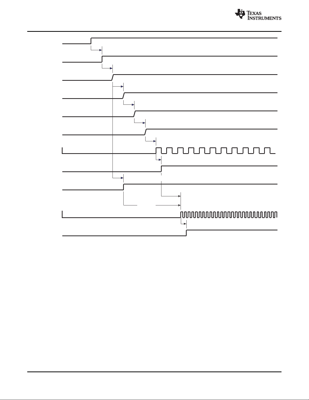
Sequence_Start
REGEN
VIO
VPLL1
VDD2
VDD1
32K OUTCLK
SYSEN
CLKEN
HFCLKOUT
NRESPWRON
4608 msbatterydetection
1068 ms-3MHzoscillatorsetting+clockswitch
1099 msforVDD2stabilizationandVDD1startramping
1179 msforVIOstabilization
1022 msforLDOstabilizationandstartDcDcramping
61 ms
~5.3ms
61 ms
1953 ms
1175 msforVDD1stabilization
1179 msforVIOstabilization
1.8V
1.8V
1.2V
1.2V
032-012
TPS65950
SWCS032E–OCTOBER 2008–REVISED JANUARY 2011
www.ti.com
Figure 4-10. Timings—OMAP3 Power-On Sequence
62 Power Module Copyright © 2008–2011, Texas Instruments Incorporated
Submit Documentation Feedback
Product Folder Link(s): TPS65950
030-022
PWRON
REGEN
VIO
VPLL1
VDD2
VDD1
32KCLKOUT
SYSEN
CLKEN
HFCLKOUT
NRESPWRON
4791 s – 3MHzoscillatorsetting+internalregm
1068 sforexternalsupplyrampm
1099 sforVDD2stabilizationm
1179 sforVIOdc-dcstablilizationm
1022 sm
1099 sforVDD2stabilizationm
61 sm
1175 sforVDD1stabilizationm
1953 sfordigitalclocksettingm
64 sm
1.8V
1.8V
1.2V
1.2V
TPS65950
www.ti.com
4.5.3.4 Power On in Slave_C021_Generic Mode
Figure 4-11 describes the timing and control that must occur in the Slave_C021_Generic mode.
Sequence_Start is a symbolic internal signal to ease the description of the power sequences and occurs
according to the different events detailed in Figure 4-8.
SWCS032E–OCTOBER 2008–REVISED JANUARY 2011
Figure 4-11. Timings—Power On in Slave_C021_Generic Model
4.5.4 Power-Off Sequence
This section describes the signal behavior required to power down the system.
4.5.4.1 Power-Off Sequence in Master Modes
Figure 4-12 shows the timing and control that occur during the power-off sequence in master modes.
Copyright © 2008–2011, Texas Instruments Incorporated Power Module 63
Submit Documentation Feedback
Product Folder Link(s): TPS65950

VBAT
DEVOFF(register)
NRESPWRON
REGEN
32K OUTCLK
DCDCs
LDOs
SYSEN
HFCLKOUT
CLKEN
NEXT_Startup_event
18 sm
1.2ms
1.2ms
1.2ms
18 sm
18 sm
18 sm
3.42msbeforedetectionofstartingevent
126 sm
032-013
TPS65950
SWCS032E–OCTOBER 2008–REVISED JANUARY 2011
www.ti.com
NOTE: All timings are typical values with the default setup (depending on the resynchronization between power domains,
64 Power Module Copyright © 2008–2011, Texas Instruments Incorporated
state machinery priority, etc.).
Figure 4-12. Power-Off Sequence in Master Modes
If the value of the HF clock is not 19.2 MHz (with the values of the CFG_BOOT HFCLK_FREQ bit field set
accordingly), the delay between DEVOFF and NRESPWRON/CLK32KOUT/SYSEN/HFCLKOUT is divided
by two (approximately 9 μs). This is caused by the internal frequency used by power STM switching from
3 to 1.5 MHz if the HF clock value is 19.2 MHz.
The DEVOFF event is PWRON falling edge in slave mode and DEVOFF internal register write in master
mode.
Submit Documentation Feedback
Product Folder Link(s): TPS65950

TPS65950
www.ti.com
5 Real-Time Clock and Embedded Power Controller
The TPS65950 device contains an RTC to provide clock and timekeeping functions and an EPC to
provide battery supervision and control.
5.1 RTC
The RTC provides the following basic functions:
• Time information (seconds/minutes/hours) directly in binary-coded decimal (BCD) code
• Calendar information (day/month/year/day of the week) directly in BCD code
• Interrupt generation periodically (1 second/1 minute/1 hour/1 day) or at a precise time (alarm function)
• 32-kHz oscillator drift compensation and time correction
• Alarm-triggered system wake-up event
5.1.1 Backup Battery
The TPS65950 implements a backup mode in which a backup battery can keep the RTC running to
maintain clock and time information even if the main supply is not present. If the backup battery is
rechargeable, the device also provides a backup battery charger so it can be recharged when the main
battery supply is present.
The backup domain powers the following:
• Internal 32.768-kHz crystal oscillator
• RTC
• Eight GP storage registers
• Backup domain low-power regulator (VBRTC)
SWCS032E–OCTOBER 2008–REVISED JANUARY 2011
5.2 EPC
The EPC provides five system states for optimal power use by the system, as listed in Table 5-1.
Three categories of events can trigger state transitions:
• Hardware events: Supply/battery insertion, wake-up requests, USB plug, and RTC alarm
• Software events: Switch-off commands, switch-on commands, and sleep-on commands
• Monitoring events: Supply/battery level check, main battery removal, main battery fail, and thermal
Table 5-1. System States
System State Description
NO SUPPLY The system is not powered by any battery.
BACKUP The system is powered only with the backup battery and maintains only the VBRTC supply.
WAIT-ON The system is powered by the main battery and maintains only the VRRTC supply. It can
accept switch-on requests.
ACTIVE The system is powered by the main battery; all supplies can be enabled with full current
capability.
SLEEP The main battery powers the system; selected supplies are enabled, but in low consumption
mode.
shutdown
Copyright © 2008–2011, Texas Instruments Incorporated Real-Time Clock and Embedded Power Controller 65
Submit Documentation Feedback
Product Folder Link(s): TPS65950
Stereoheadset
Stereo
hands-free
classD
Monoearpiece
Mainmicrophone
Submicrophone
Headsetmicrophone
Stereoauxiliary
input
Digital
microphones
(upto4)
Voice
PCM
interface
Audio
TDM/I2S
interface
High-speed
I C
2
(control)
Audio/voicemodule
HFCLKIN
BiasLDOs
(x3)
Carkit/MCPC
speaker/
microphone
Bluetooth
PCM
interface
Vibrator
H-bridge
Device
032-014
TPS65950
SWCS032E–OCTOBER 2008–REVISED JANUARY 2011
6 Audio/Voice Module
The audio codec in the device includes five DACs and two ADCs to provide multiple voice channels and
stereo downlink channels that can support all standard audio sample rates through I2S/TDM format
interfaces. The audio output stages on the device include stereo headset amplifiers, two integrated
class-D amplifiers providing stereo differential outputs, predrivers for line outputs, and an earpiece
amplifier. The input audio stages include three differential microphone inputs, stereo line inputs, and
interface for digital micrphones. Automatic and programmable gain control is available with all necessary
digital filtering, side-tone functions, and pop-noise reduction.
Figure 6-1 is a block diagram of the audio/voice module.
www.ti.com
66 Audio/Voice Module Copyright © 2008–2011, Texas Instruments Incorporated
Figure 6-1. Audio/Voice Module Block Diagram
Submit Documentation Feedback
Product Folder Link(s): TPS65950

DigitalPGA
Gain=0dB
AnalogPGA
Gain=2dB
Amp
6dB
DAC
4.0Vppdiff
0dBFs
032-015
TPS65950
www.ti.com
6.1 Audio/Voice Downlink (RX) Module
The audio/voice module includes the following output stages:
• Mono/stereo single-ended headset amplifier
• Stereo differential integrated class-D 8-Ω hands-free amplifiers
• Predriver output signals for external class-D amplifiers (single-ended)
• Mono differential earpiece amplifier
• Vibrator H-bridge
6.1.1 Earphone Output
6.1.1.1 Earphone Output Characteristics
Analog signals from the audio and/or voice interface are fed to the earphone amplifier. This amplifier, with
different gains, provides a full differential signal on terminals EARP and EARM. Figure 6-2 shows the
earphone amplifier. Table 6-1 lists the output characterstics of the earphone amplifier.
Figure 6-2. Earphone Amplifier
SWCS032E–OCTOBER 2008–REVISED JANUARY 2011
Table 6-1. Earphone Amplifier Output Characteristics
Parameter Test Conditions Min Typ Max Unit
Differential load impedance 26 32 Ω
100 100 pF
Gain range
Absolute gain error –1 1 dB
Maximum output power At 1.4 Vrms differential output voltage 61.25 mW
Peak-to-peak differential output voltage (0 dBFs) Default gain
Total harmonic distortion At 0 dBFs –65 –60
Default gain
Load impedance = 32 Ω At –20 dBFs –60
Idle channel noise Gain = 0 dB –90 –85 dBFs
(20 Hz to 20 kHz, A-weighted) Load = 32 Ω
Output PSRR (for all gains) 20 Hz to 4 kHz 90
(1) Audio digital filter = –62 to 0 dB (1-dB steps) and 0 to 12 dB (6-dB steps)
(2) The default gain setting assumes the ARXPGA has 2-dB gain setting (volume control) and output driver at 6-dB gain setting.
(1)
(2)
Voice digital filter = –36 to 12 dB (1-dB steps)
ARXPGA (volume control) = –24 to 12 dB (2-dB steps)
Output driver = 0, 6, 12 dB
Audio path –86 36 dB
Voice path –60 36
Load impedance = 32 Ω
(2)
At –6 dBFs –70 –65 dB
At –60 dBFs –30
20 Hz to 20 kHz 70
4.0 V
dB
PP
Copyright © 2008–2011, Texas Instruments Incorporated Audio/Voice Module 67
Submit Documentation Feedback
Product Folder Link(s): TPS65950

32
W
EARM
EARP
OnBoard
Chip
C
EAR
032-016
DigitalPGA
Gain=0dB
AnalogPGA
Gain=0dB
Amp
10.4dB
DAC
5.0Vppdiff
032-017
TPS65950
SWCS032E–OCTOBER 2008–REVISED JANUARY 2011
6.1.1.2 External Components and Application Schematic
Figure 6-3 is a simplified schematic of the earphone speaker.
www.ti.com
Figure 6-3. Earphone Speaker
NOTE
For the component values, see Table 15-1.
6.1.2 8-Ω Stereo Hands-Free
The digital signal from the audio and/or voice interface is fed to two class-D amplifiers. These 8-Ω speaker
amplifiers provide a stereo differential signal on terminal pairs (IHF.RIGHT.P, IHF.RIGHT.M and
IHF.LEFT.P, IHF.LEFT.M).
6.1.2.1 8-Ω Stereo Hands-Free Output Characteristics
Figure 6-4 shows the 8-Ω stereo hands-free amplifier. Table 6-2 lists the output characteristics of the 8-Ω
stereo hands-free amplifier.
Figure 6-4. 8-Ω Stereo Hands-Free Amplifiers
Table 6-2. 8-Ω Stereo Hands-Free Output Characteristics
Parameter Test Conditions Min Typ Max Unit
VBAT voltage 3.0 3.6 4.6 V
Load impedance 6 8 Ω
68 Audio/Voice Module Copyright © 2008–2011, Texas Instruments Incorporated
Submit Documentation Feedback
Product Folder Link(s): TPS65950

TPS65950
www.ti.com
SWCS032E–OCTOBER 2008–REVISED JANUARY 2011
Table 6-2. 8-Ω Stereo Hands-Free Output Characteristics (continued)
Parameter Test Conditions Min Typ Max Unit
Gain range
Absolute gain error –1 1 dB
Maximum output power (load impedance = 8 Ω) VBAT > 3.6 V 400 mW
Peak-to-peak differential output voltage VBAT> 3.6 V (0 dBFs) 5.0 V
Total harmonic distortion (load impedance = 8 Ω, gain setting = 0
dB) At –10 dBFs –60
(VBAT > 3.6 V)
Total harmonic distortion (load impedance = 8 Ω, (VBAT > 4.2 V) 2 dBFs –60 –40 dB
Idle channel noise (20 Hz to 20 kHz) 0 dB gain –88 dBFs
PSRR (input signal 1 kHz sine, 300 mVPP GSM ripple at 217 Hz From VBAT 75 80 dB
with 10-μs rise/fall times, at 12.5% duty cycle)
Efficiency
Power dissipation Power on load = 400 mW 175 mW
Idle current consumption on VBAT Without input signal 6 mA
Clock frequency for the ramp generation 384 426.6 kHz
I
DDQ
(1) Audio digital filter = –62 to 0 dB (1-dB steps) and 0 to 12 dB (6-dB steps)
(1)
current At 25°C 0.6 μA
Voice digital filter = –36 to 12 dB (1-dB steps)
ARXPGA (volume control) = –24 to 12 dB (2-dB steps)
Output driver = 10.4 dB
Audio path –75.6 34.4 dB
Voice path –49.6 34.4
VBAT > 4.0 V 700
VBAT > 4.0 V (2 dBFs) 6.25
At 0 dBFs –60 –40 dBFs
At –20 dBFs –45
At –60 dBFs –20
Power on load = 400 mW 70%
Load impedance = 8 Ω
Load impedance = 8 Ω
PP
6.1.2.1.1 Short-Circuit Protection
There is short-circuit protection for hands-free amplifiers to limit power dissipation to 1.2 W. The
short-circuit protection can be disabled by register. If a short circuit is detected, the short-circuit detection
block switches off the hands-free speaker output stages. A software restart is required to restart the
class-D amplifier.
6.1.2.2 External Components and Application Schematic
Figure 6-5 is a simplified schematic of the 8-Ω stereo hands-free.
Copyright © 2008–2011, Texas Instruments Incorporated Audio/Voice Module 69
Submit Documentation Feedback
Product Folder Link(s): TPS65950

8 W
Ferrite chip bead
Ferrite chip bead
VBAT.RIGHT/LEFT
IHF.RIGHT/LEFT.M
GND.RIGHT/LEFT
C /C
HFR HFL
IHF.RIGHT/LEFT.P
VBAT
On board
Chip
032-018
L /L
HFR.P HFL.P
L /L
HFR.M HFL.M
C /C
HFR.P HFL.P
C /C
HFR.M HFL.M
DigitalPGA
Gain=0dB
AnalogPGA
Gain=0dB
Amp
0dB
DAC
1.5Vpp
0dBFs
032-019
TPS65950
SWCS032E–OCTOBER 2008–REVISED JANUARY 2011
Figure 6-5. 8-Ω Stereo Hands-Free
www.ti.com
For the component values, see Table 15-1.
For ferrite bead, choose one with high impedance at high frequencies, but with very low impedance at low
frequencies. For example, MPZ1608S221A (recommended), N2012ZPS121, or MDP BKP1608HS271.
6.1.3 Headset
The analog signal from the audio and/or voice interface is fed to two single-ended headset amplifiers.
There are two configurations:
• Stereo single-ended mode: Left and right headset amplifiers with different gains (–6, 0, 6 dB) provide
the stereo signal on the HSOL and HSOR terminals. A pseudo-ground is provided on the VMID
terminal to eliminate external capacitors.
• Stereo single-ended mode ac-coupled: Left and right headset amplifiers with different gains (–6, 0, 6
dB) provide the stereo signal on the HSOL and HSOR terminals. The external capacitor is required to
eliminate the dc component of the signal.
6.1.3.1 Headset Output Characteristics
Figure 6-6 shows the headset amplifier. Table 6-3 lists the output characteristics of the headset amplifier.
NOTE
Parameter Test Conditions Min Typ Max Unit
Load impedance 14 16 Ω
70 Audio/Voice Module Copyright © 2008–2011, Texas Instruments Incorporated
Figure 6-6. Headset Amplifier
Table 6-3. Headset Output Characteristics
Submit Documentation Feedback
Product Folder Link(s): TPS65950

TPS65950
www.ti.com
SWCS032E–OCTOBER 2008–REVISED JANUARY 2011
Table 6-3. Headset Output Characteristics (continued)
Parameter Test Conditions Min Typ Max Unit
100 100 pF
Gain range
Absolute gain error –1 1 dB
Maximum output power
Peak-to-peak output voltage (0 dBFs) Default gain
Total harmonic distortion At 0 dBFs –80 –75 dB
Default gain
Load = 16 Ω At –20 dBFs –70 –65
Idle channel noise Default gain
(20 Hz to 20 kHz, A-weighted) Load = 16 Ω
SNR (A-weighted over 20-kHz bandwidth) At 0 dBFs 82 86 dB
Output PSRR (for all gains) 20 Hz to 4 kHz 90 dB
Crosstalk between right and left channels –60 dB
Total harmonic distortion At 0 dBFs –75 –70 dB
Default gain
Load = 16 Ω At –20 dBFs –70 –65
Idle channel noise Default gain
(20 Hz to 20 kHz, A-weighted) Load = 16 Ω
Output PSRR (for all gains) 20 Hz to 4 kHz 85 dB
(1) Audio digital filter = –62 to 0 dB (1-dB steps) and 0 to 12 dB (6-dB steps)
(2) The default gain setting assumes the ARXPGA has 0 dB gain setting (volume control) and output driver at 0 dB gain setting.
(3) The default gain setting assumes the ARXPGA has 0 dB gain setting (volume control) and output driver at 0 dB gain setting.
(1)
Single-Ended Mode ac-Coupled
(2)
Single-Ended Mode (Pseudo-Ground Provided on HSOVMID)
(3)
Voice digital filter = –36 to 12 dB (1-dB steps)
ARXPGA (volume control) = –24 to 12 dB (2-dB steps)
Output driver = –6, 0, 6 dB
Audio path –92 30 dB
Voice path –66 30
At 0.53 Vrms differential output voltage 17.56 mW
Load impedance = 16 Ω
(2)
1.5 V
At –6 dBFs –74 –69
At –60 dBFs –30 –25
(3)
–90 –85 dB
20 Hz to 20 kHz 70
At –6 dBFs –74 –69
At –60 dBFs –30 –25
(3)
–90 –85 dB
20 Hz to 20 kHz 65
PP
Copyright © 2008–2011, Texas Instruments Incorporated Audio/Voice Module 71
Submit Documentation Feedback
Product Folder Link(s): TPS65950

Onboard
Chip
4-wirestereojack
HSOR
HSOL
Cl
Cl
Rb
HSMIC.M
HSMIC.P
VHSMIC .OUT
Cb
Rs
Rs
Rl
Rl
Rsb
Cs
Cs
C
HM.P
C
HM.M
C
HM.O
032-20
TPS65950
SWCS032E–OCTOBER 2008–REVISED JANUARY 2011
6.1.3.2 External Components and Application Schematic
Figure 6-7 is a schematic of a headset 4-wire stereo jack without an external FET. Table 6-4 lists the
output characteristics of this configuration.
www.ti.com
Figure 6-7. Headset 4-Wire Stereo Jack Without an External FET
Table 6-4. Output Characteristics of a Headset 4-Wire Stereo Jack Without an External FET
Parameter Test Conditions Min Typ Max Unit
Rsb Cb < 200 pF 0 Ω
Cb = 100 nF 300
Cb = 1 μF 500
Rb + Rsb 2.2 2.7 kΩ
Cs 22 47 μF
The input capacitors and output resistors form a
high-pass filter (HPF) with the corner frequency =
1/(2πR
Rs required to ensure 16 to 32 Ω <100 pF 0 Ω
HS amplifier stability 16 to 32 Ω 1 nF 4
72 Audio/Voice Module Copyright © 2008–2011, Texas Instruments Incorporated
out
/Cs)
R
L
16 Ω 2 nF 8
24 Ω 12
Submit Documentation Feedback
Product Folder Link(s): TPS65950
32 Ω 18
16 Ω 3 nF 12
24 Ω 20
32 Ω 24
16 Ω 4 nF 16
24 Ω 24
32 Ω 32
16 Ω 5 nF 20
24 Ω 28
32 Ω 36
C
L

Onboard
Chip
4-wirestereojack
HSOR
HSOL
Cl
Cl
Rb
HSMIC . M
HSMIC .P
VHSMIC .OUT
Cb
Rs
Rs
Rl
Rl
Rsb
C
s
C
s
GPIO_6 ( MUTE )
ExternalFET
C
HM.O
C
HM.P
C
HM.M
032-021
TPS65950
www.ti.com
Table 6-5 is a schematic of a headset 4-wire stereo jack with an external FET. Table 6-5 lists the output
characteristics of this configuration.
SWCS032E–OCTOBER 2008–REVISED JANUARY 2011
NOTE
For other component values, see Table 15-1.
Figure 6-8. Headset 4-Wire Stereo Jack With an External FET
Table 6-5. Output Characteristics of a Headset 4-Wire Stereo Jack With an External FET
Parameter Test Conditions Min Typ Max Unit
Rsb Cb < 200 pF 0 Ω
Cb = 100 nF 300
Cb = 1 μF 500
Rb + Rsb 2.2 2.7 kΩ
Cs 22 47 μF
The input capacitors and output resistors form a HPF with
the corner frequency = 1/(2πR
Rs required to ensure HS amplifier stability and no 16 Ω <2 nF 10 Ω
distortion caused by the parasitic diode of the external
FET
out
/Cs)
R
L
24 Ω 15
C
L
32 Ω 20
16 Ω 3 nF 12
24 Ω 20
32 Ω 24
16 Ω 4 nF 16
24 Ω 24
32 Ω 32
16 Ω 5 nF 20
24 Ω 28
32 Ω 36
Copyright © 2008–2011, Texas Instruments Incorporated Audio/Voice Module 73
Submit Documentation Feedback
Product Folder Link(s): TPS65950

Onboard
Chip
5-wirestereojack
HSOR
HSOL
Cl
Cl
Rb
HSMIC.M
HSMIC.P
VHSMIC.OUT
Cb
Rs
Rs
Rl
Rl
Rsb
HSOVMID
C
HM.O
C
HM.P
C
HM.M
C
HM.O
032-022
TPS65950
SWCS032E–OCTOBER 2008–REVISED JANUARY 2011
For other component values, see Table 15-1.
Figure 6-9 is a schematic of a headset 5-wire stereo jack. Table 6-6 lists the output characteristics of this
configuration.
www.ti.com
NOTE
Figure 6-9. Headset 5-Wire Stereo Jack
Table 6-6. Output Characteristics of a Headset 5-Wire Stereo Jack
Parameter Test Conditions Min Typ Max Unit
Rsb Cb < 200 pF 0 Ω
Cb = 100 nF 300
Cb = 1 μF 500
Rb + Rsb 2.2 2.7 kΩ
R
L
Rs required to ensure HS amplifier stability 16 to 32 Ω <100 pF 0 Ω
16 to 32 Ω 1 nF 4
16 Ω 2 nF 8
24 Ω 12
32 Ω 18
16 Ω 3 nF 12
24 Ω 20
32 Ω 24
16 Ω 4 nF 16
24 Ω 24
32 Ω 32
16 Ω 5 nF 20
24 Ω 28
32 Ω 36
74 Audio/Voice Module Copyright © 2008–2011, Texas Instruments Incorporated
Submit Documentation Feedback
Product Folder Link(s): TPS65950
C
L

HSMIC.M
HSMIC
Onboard Chip
Rb
VHSMIC.OUT
4-wirestereojack
HSOR
HSOL
Cl
Cs
Cl
Rs
Rs
Cb
Cs
Rl
Rl
Rsb
+
–
mA
+
–
mA
mA
C
HM.P
Gain= –1
C
HM.M
C
HM.O
032-023
Ampli_HS
Ampli_HS
TPS65950
www.ti.com
Figure 6-10 is a schematic of a headset 4-wire stereo jack optimized.
SWCS032E–OCTOBER 2008–REVISED JANUARY 2011
NOTE
For other component values, see Table 15-1.
Figure 6-10. Headset 4-Wire Stereo Jack Optimized
NOTE
For other component values, see Table 15-1.
6.1.4 Headset Pop-Noise Attenuation
Pop noise occurs when the audio output amplifier is switched on. Although the speaker is ac-coupled
through an external capacitor, the sharp rise time given by the activation of the amplifier causes a large
spike to propagate to the speakers. Pop attenuation is achieved through a precharge and discharge of the
external coupling capacitor.
The antipop system using an internal current generator controlling the ramp of charge or discharge is
implemented for the headset output. The pop-noise effect can be dramatically reduced by an external FET
controlled by a 1.8-V output signal (MUTE pin).
Figure 6-11 is a diagram of headset pop noise. Table 6-7 lists the characteristics of headset pop noise.
Copyright © 2008–2011, Texas Instruments Incorporated Audio/Voice Module 75
Submit Documentation Feedback
Product Folder Link(s): TPS65950
HSO
EXTMUTE
V
0
VMID
t
VMID_EN
HSR/L_GAIN(1:0)
RAMP_EN
0
0
MUTE
HSO
RAMP_DELAY
Application
mode
t
t
RAMP_DELAY
032-024
dV/dt
TPS65950
SWCS032E–OCTOBER 2008–REVISED JANUARY 2011
www.ti.com
dv/dt Ramp of charge or discharge 170 V/s
Pop-noise (A-weighted) ac-coupling capacitor = 47 μF 1 mV
6.1.5 Predriver for External Class-D Amplifier
Figure 6-11. Headset Pop-Noise Cancellation Diagram
Table 6-7. Headset Pop-Noise Characteristics
Parameter Test Conditions Min Typ Max Unit
Serial resistor = 33 Ω
External FET: Rdson = 0.12 Ω
Two predriver amplifiers provide a stereo signal on the PreD.LEFT and PreD.RIGHT terminals to drive an
external class-D amplifier. These terminals are available if a stereo, single-ended, ac-coupled headset is
used.
6.1.5.1 Predriver Output Characteristics
Table 6-8 lists the output characteristics of the predriver.
76 Audio/Voice Module Copyright © 2008–2011, Texas Instruments Incorporated
Submit Documentation Feedback
Product Folder Link(s): TPS65950

PreDriverD
Onboard
Chip
ClassD
(TPA2010D1...)
IN+
IN–
Closedto
external
classC
C /C
PL PR
032-025
C /C
PR.O PL.O
R /R
PL.O PR.O
C /C
PL.M PR.M
R /R
PR PL
R /R
PR.M PL.M
TPS65950
www.ti.com
SWCS032E–OCTOBER 2008–REVISED JANUARY 2011
Table 6-8. Predriver Output Characteristics
Parameter Test Conditions Min Typ Max Unit
Load impedance 10 kΩ
50 pF
Gain range
Absolute gain error –1 1 dB
Peak-to-peak output voltage (0 dBFs) Default gain
Total harmonic distortion At 0 dBFs –80 –75 dB
Default gain
Load > 10 kΩ // 50 pF At –20 dBFs –70 –65
Idle channel noise (20 Hz to 20 kHz, A-weighted)
SNR (A-weighted over 20-kHz bandwidth) At 0 dBFs 83 88 dB
Default gain
Output PSRR (for all gains) 20 Hz to 4 kHz 90 dB
(1) Audio digital filter = –62 to 0 dB (1-dB steps) and 0 to 12 dB (6-dB steps)
(2) The default gain setting assumes the ARXPGA has a 0 dB gain setting (volume control) and output driver has a 0 dB gain setting.
(3) The default gain setting assumes the ARXPGA has a 0 dB gain setting (volume control) and output driver has a 0 dB gain setting.
(1)
(2)
(3)
Voice digital filter = –36 to 12 dB (1-dB steps)
ARXPGA (volume control) = –24 to 12 dB (2-dB steps)
Output driver = –6, 0, 6 dB
Audio path –92 30 dB
Voice path –66 30
(2)
1.5 V
At –6 dBFs –74 –69
At –60 dBFs –30 –25
Default gain
(3)
–90 –85 dB
Load = 10 Ω
At –60 dBFS 30
20 Hz to 20 kHz 70
PP
6.1.5.2 External Components and Application Schematic
Figure 6-12 is a simplified schematic of the external class-D predriver.
Figure 6-12. Predriver for External Class D
In Figure 6-12, input resistor (RPRor RPL) sets the gain of the external class D. For TPS2010D1, the gain
is defined according to the following equation:
Gain (V/V) = 2*150*103/(RPRor RPL)
RPRor RPL> 15 kΩ
Copyright © 2008–2011, Texas Instruments Incorporated Audio/Voice Module 77
Submit Documentation Feedback
Product Folder Link(s): TPS65950

Ferrite chip bead
Ferrite chip bead
VBAT.RIGHT
VIBRA.M
VIBRA.GND (LED.GND)
C
V.V
VIBRA.P
VBAT
On board
Chip
Vibrator
032-026
L
V.P
C
V.P
C
V.M
L
V.M
TPS65950
SWCS032E–OCTOBER 2008–REVISED JANUARY 2011
www.ti.com
NOTE
For other component values, see Table 15-1.
6.1.6 Vibrator H-Bridge
A digital signal from the pulse width modulated generator is fed to the vibrator H-bridge driver. The vibrator
H-bridge is a differential driver that drives vibrator motors. The differential output allows dual rotation
directions.
6.1.6.1 Vibrator H-Bridge Output Characteristics
Table 6-9 lists the output characteristics of the vibrator H-bridge.
Table 6-9. Vibrator H-Bridge Output Characteristics
Parameter Test Conditions Min Typ Max Unit
VBAT voltage 2.8 3.6 4.8 V
Differential output swing (16-Ω load) VBAT = 2.8 V 3.6 V
VBAT = 3.5 V 4.3
Output resistance (summed for both sides) 8 Ω
Load capacitance 100 pF
Load resistance 8 16 60 Ω
Load inductance 30 300 μH
Total harmonic distortion 10%
Operating frequency 20 10k Hz
PP
6.1.6.2 External Components and Application Schematic
Figure 6-13 is a simplified schematic of the vibrator H-bridge.
Figure 6-13. Vibrator H-Bridge
78 Audio/Voice Module Copyright © 2008–2011, Texas Instruments Incorporated
Submit Documentation Feedback
Product Folder Link(s): TPS65950

DigitalPGA
Gain=0dB
AnalogPGA
Gain=0dB
Amp
0dB
DAC
1.35VPP
0dBFs
USB
Amp
–0.6dB
032-027
TPS65950
www.ti.com
For other component values, see Table 15-1.
Example of ferrite: BLM 18BD221SN1.
6.1.7 Carkit Output
The USB-CEA carkit uses the DP/DM pad to output audio signals (see the CEA-936A: Mini-USB Analog
Carkit Interface Specification).
The MCPC carkit uses the RXAF analog pad to output audio signals.
Figure 6-14 shows the carkit output downlink full path characteristics for audio and USB.
SWCS032E–OCTOBER 2008–REVISED JANUARY 2011
NOTE
Figure 6-14. Carkit Output Downlink Path Characteristics
Table 6-10 lists the electrical characteristics of the MCPC and USB-CEA carkit audio.
Table 6-10. MCPC and USB-CEA Carkit Audio Downlink Electrical Characteristics
Parameter Conditions Min Typ Max Unit
Output load USB-CEA (DP/DM) 20 kΩ
MCPC (RXAF) 5
Gain range
Absolute gain error At 1 kHz –1 1 dB
Peak-to-peak differential output voltage (0 dBFs) Gain = 0 dB 1.5 V
Total harmonic distortion At 0 dBFs –80 –75 dB
THD+N (20 Hz to 20 kHz, A-weighted) At 0 dBFs 60 dB
Idle channel noise (20 Hz to 20 kHz, A-weighted), default gain USB-CEA –77 dBFs
setting
Output PSRR 20 Hz to 20 kHz 60 dB
Supply voltage (VINTANA1) 1.5 V
Common mode output voltage for USB-CEA 1.3 1.35 1.4 V
Isolation between D+/D– during audio mode (20 Hz to 20 kHz) 60 dB
Crosstalk between right and left channels USB-CEA stereo –90 dB
Crosstalk RX/TX (1 VPPoutput) USB-CEA mono/stereo –60 dB
Signal noise ratio (20 Hz to 20 kHz, A-weighted) At 0 dBFs 60 dB
(1)
(2)
Audio path –92 30 dB
Voice path –66 30
PP
At –6 dBFs –74 –69
At –20 dBFs –70 –65
At –60 dBFs –30 –25
MCPC –80 –77
MCPC –65
(1) Audio digital filter = –62 to 0 dB (1-dB steps) and 0 to 12 dB (6-dB steps);
Voice digital filter = –36 to 12 dB (1-dB steps);
ARXPGA (volume control) = –24 to 12 dB (2-dB steps);
Output driver (USB-CEA and MCPC) = –1 dB
(2) The default gain setting assumes the ARXPGA has 0-dB gain setting (volume control) and output driver at 0.6-dB gain setting.
Copyright © 2008–2011, Texas Instruments Incorporated Audio/Voice Module 79
Submit Documentation Feedback
Product Folder Link(s): TPS65950

Low-pass
filter
Digital
modulator
Randomizer
High-pass
filter
Audiointerface
DAC
032-028
Low-pass
filter
Digital
modulator
Randomizer
High-pass
filter
Voiceinterface
DAC
032-029
TPS65950
SWCS032E–OCTOBER 2008–REVISED JANUARY 2011
www.ti.com
Table 6-10. MCPC and USB-CEA Carkit Audio Downlink Electrical Characteristics (continued)
Parameter Conditions Min Typ Max Unit
Phone speaker amplifier output impedance at 1 kHz USB-CEA (DP/DM) 200 Ω
MCPC (RXAF) 200
6.1.8 Digital Audio Filter Module
Figure 6-15 shows the digital audio filter downlink full path characteristics of the audio interface.
Figure 6-15. Digital Audio Filter Downlink Path Characteristics
The HPF can be bypassed.
Table 6-11 lists the audio filter frequency responses relative to reference gain at 1 kHz.
Table 6-11. Digital Audio Filter RX Electrical Characteristics
Parameter Conditions Min Typ Max Unit
Passband 0.42 F
Passband ripple 0 to 0.42F
Stopband 0.6 F
Stopband attenuation F = 0.6F
Group delay 15.8/F
Linear phase –1.4 1.4 °
(1) FSis the sampling frequency (8, 11.025, 12, 16, 22.05, 24, 32, 44.1, or 48 kHz).
(1)
S
(1)
to 0.8F
S
(1)
S
–0.25 0.1 0.25 dB
60 75 dB
(1)
S
6.1.9 Digital Voice Filter Module
Figure 6-16 shows the digital voice filter downlink full path characteristics of the voice interface.
Figure 6-16. Digital Voice Filter Downlink Path Characteristics
S
S
μs
The global HPF or only the third-order HPF can be bypassed (when the third-order HPF is skipped, the
first-order HPF remains active).
80 Audio/Voice Module Copyright © 2008–2011, Texas Instruments Incorporated
Submit Documentation Feedback
Product Folder Link(s): TPS65950

–3
–2.5
–2
–1.5
–1
–0.5
0
0.5
1
1.5
2
0 500 1000 1500 2000 2500 3000 3500 4000
Rx_8K_1st_HPF
Specification
Rx_8K_3rd_HPF
VoiceDownlink(RX)Filter8kHz
Frequency(Hz)
Gain(dB)
032-030
TPS65950
www.ti.com
6.1.9.1 Voice Downlink Filter (Sampling Frequency at 8 kHz)
Figure 6-17 shows the voice downlink frequency response with FS= 8 kHz. Table 6-12 lists the voice filter
frequency responses relative to the reference gain at 1 kHz with FS= 8 kHz.
SWCS032E–OCTOBER 2008–REVISED JANUARY 2011
Figure 6-17. Voice Downlink Frequency Response With FS= 8 kHz
Table 6-12. Digital Voice Filter RX Electrical Characteristics With FS= 8 kHz
Parameter Test Conditions Min Typ Max Unit
Frequency response relative to reference gain at 1 kHz (first-order 100 Hz –20 dB
HPF)
Pole when third-order HPF is disabled (first-order HPF) 2.5 Hz
Group delay 0.5 ms
Copyright © 2008–2011, Texas Instruments Incorporated Audio/Voice Module 81
200 Hz –8 –0.5
300 to 3300 Hz –0.5 0 0.5
3400 Hz –1.5 0 0.1
4000 Hz –17
4600 Hz –40
> 6000 Hz –45
Submit Documentation Feedback
Product Folder Link(s): TPS65950
–3
–2.5
–2
–1.5
–1
–0.5
0
0.5
1
1.5
2
0 1000 2000 3000 4000 5000 6000 7000
Rx_8K_1st_HPF
Rx_8K_3rd_HPF
Specification
Frequency(Hz)
VoiceDownlink(RX)Filter16kHz
032-031
Gain(dB)
TPS65950
SWCS032E–OCTOBER 2008–REVISED JANUARY 2011
6.1.9.2 Voice Downlink Filter (Sampling Frequency at 16 kHz)
Figure 6-18 shows the voice downlink frequency response with FS= 16 kHz. Table 6-13 lists the voice
filter frequency responses relative to the reference gain at 1 kHz with FS= 16 kHz.
www.ti.com
Figure 6-18. Voice Downlink Frequency Response With FS= 16 kHz
Table 6-13. Digital Voice Filter RX Electrical Characteristics With FS= 16 kHz
Parameter Test Conditions Min Typ Max Unit
Frequency response relative to reference gain at 1 kHz (first-order 300 to 6600 Hz –0.5 0 0.5 dB
HPF)
Pole when third-order HPF is disabled (first-order HPF) 5 Hz
6.1.10 Boost Stage
The boost effect adds emphasis to low frequencies. It compensates for an HPF created by the
capacitance resistor (CR) filter of the headset (in ac-coupling configuration).
There are four modes. Three effects are available, with slightly different frequency responses, and the
fourth setting disables the boost effect:
• Boost effect 1
• Boost effect 2
• Boost effect 3
• Flat equalization: The boost effect is in bypass mode.
Table 6-14 and Table 6-15 list typical values according to frequency response versus input frequency and
FSfrequency.
82 Audio/Voice Module Copyright © 2008–2011, Texas Instruments Incorporated
6800 Hz –1.5 0 0.1
8000 Hz –17
9200 Hz –40
> 12000 Hz –45
Submit Documentation Feedback
Product Folder Link(s): TPS65950

TPS65950
www.ti.com
SWCS032E–OCTOBER 2008–REVISED JANUARY 2011
Table 6-14. Boost Electrical Characteristics Versus FSFrequency (FS≤ 22.05 kHz)
Frequency
(Hz)
10 4.51 5.13 5.62 5.10 5.51 5.80 5.22 5.58 5.83 5.54 5.77 5.92 5.76 5.89 5.97
12 4.08 4.83 5.46 4.80 5.32 5.71 4.95 5.41 5.76 5.36 5.66 5.87 5.65 5.83 5.94
15.2 3.43 4.32 5.18 4.28 4.97 5.54 4.47 5.11 5.61 5.03 5.47 5.79 5.45 5.71 5.90
18.2 2.91 3.86 4.89 3.82 4.63 5.36 4.04 4.80 5.45 4.71 5.26 5.69 5.24 5.59 5.84
20.5 2.56 3.53 4.65 3.49 4.37 5.21 3.72 4.56 5.32 4.45 5.09 5.60 5.06 5.49 5.79
29.4 1.62 2.49 3.78 2.45 3.42 4.57 2.68 3.74 4.73 3.51 4.39 5.24 4.35 5.02 5.59
39.7 1.05 1.71 2.93 1.67 2.55 3.84 1.88 2.80 4.06 2.66 3.63 4.72 3.67 4.45 5.27
50.4 0.71 1.20 2.26 1.17 1.91 3.17 1.33 2.13 3.41 2.01 2.95 4.19 2.89 3.85 4.88
60.3 0.51 0.92 1.79 0.89 1.49 2.65 1.00 1.68 2.89 1.57 2.43 3.72 2.39 3.35 4.52
76.7 0.32 0.61 1.26 0.59 1.05 1.99 0.69 1.18 2.22 1.11 1.79 3.04 1.76 2.66 3.94
97.5 0.20 0.39 0.87 0.38 0.70 1.43 0.44 0.79 1.62 0.75 1.27 2.36 1.24 2.00 3.28
131.5 0.12 0.21 0.50 0.20 0.39 0.88 0.25 0.47 1.02 0.42 0.78 1.59 0.75 1.30 2.41
157 0.08 0.15 0.36 0.15 0.28 0.65 0.17 0.33 0.75 0.31 0.57 1.22 0.55 0.99 1.93
200 0.05 0.09 0.22 0.09 0.17 0.41 0.11 0.21 0.49 0.19 0.37 0.82 0.36 0.66 1.38
240 0.03 0.06 0.15 0.06 0.12 0.29 0.07 0.14 0.35 0.14 0.26 0.60 0.25 0.48 1.04
304 0.02 0.04 0.09 0.04 0.07 0.18 0.04 0.09 0.22 0.08 0.16 0.38 0.16 0.30 0.70
463 0.00 0.01 0.03 0.01 0.03 0.07 0.02 0.04 0.09 0.03 0.07 0.17 0.07 0.13 0.32
704 0.00 0.00 0.01 0.00 0.01 0.03 0.01 0.01 0.03 0.01 0.03 0.07 0.03 0.06 0.14
1008 0.00 0.00 0.00 0.00 0.00 0.01 0.00 0.00 0.01 0.00 0.01 0.03 0.01 0.02 0.06
1444 0.00 0.00 0.00 0.00 0.00 0.00 0.00 0.00 0.00 0.00 0.00 0.00 0.00 0.01 0.02
2070 0.00 0.00 0.00 0.00 0.00 0.00 0.00 0.00 0.00 0.00 0.00 0.00 0.00 0.00 0.01
3770 0.00 0.00 0.00 0.00 0.00 0.00 0.00 0.00 0.00 0.00 0.00 0.00 0.00 0.00 0.00
FS= 8 kHz FS= 11.025 kHz FS= 12 kHz FS= 16 kHz FS= 22.05 kHz
1 2 3 1 2 3 1 2 3 1 2 3 1 2 3
Unit
dB
Table 6-15. Boost Electrical Characteristics Versus FSFrequency (FS≥ 24 kHz)
Frequency
(Hz)
10 5.79 5.90 5.97 5.89 5.89 5.99 5.95 5.98 6.04 5.96 5.99 6.01 5.71 5.83 5.90
12 5.70 5.85 5.95 5.84 5.84 5.98 5.92 5.97 6.03 5.94 5.98 6.00 5.54 5.68 5.81
15.2 5.53 5.76 5.91 5.73 5.73 5.96 5.87 5.94 6.02 5.89 5.95 5.99 5.40 5.57 5.73
18.2 5.35 5.65 5.87 5.62 5.62 5.93 5.80 5.90 6.00 5.83 5.93 5.98 5.28 5.48 5.68
20.5 5.19 5.56 5.83 5.52 5.52 5.91 5.74 5.87 5.99 5.78 5.90 5.97 5.19 5.42 5.64
29.4 4.55 5.18 5.64 5.10 5.07 5.79 5.51 5.75 5.94 5.57 5.79 5.92 4.87 5.18 5.48
39.7 3.81 4.62 5.37 4.52 4.52 5.64 5.12 5.53 5.85 5.26 5.59 5.84 4.47 4.91 5.30
50.4 3.14 4.06 5.02 3.94 3.95 5.43 4.69 5.27 5.72 4.88 5.37 5.73 4.08 4.63 5.11
60.3 2.62 3.51 4.69 3.46 3.54 5.21 4.30 5.00 5.59 4.49 5.13 5.62 3.72 4.37 4.95
76.7 1.97 2.90 4.15 2.76 2.76 4.78 3.68 4.52 5.34 3.91 4.70 5.40 3.18 3.92 4.67
97.5 1.41 2.22 3.51 2.10 2.09 4.27 2.99 3.94 4.99 3.24 4.15 5.07 2.59 3.41 4.33
131.5 0.88 1.49 2.65 1.40 1.40 3.49 2.15 3.10 4.35 2.38 3.35 4.51 1.86 2.69 3.75
157 0.65 1.13 2.15 1.04 1.04 2.96 1.70 2.58 3.90 1.90 2.82 4.08 1.47 2.24 3.35
200 0.41 0.76 1.55 0.70 0.70 2.28 1.19 1.93 3.23 1.35 2.15 3.44 1.03 1.68 2.77
240 0.30 0.55 1.18 0.50 0.50 1.81 0.89 1.51 2.71 1.02 1.70 2.92 0.77 1.31 2.32
304 0.18 0.35 0.80 0.33 0.32 1.27 0.58 1.04 2.05 0.68 1.19 2.24 0.51 0.90 1.75
463 0.08 0.16 0.37 0.14 0.14 0.64 0.27 0.50 1.12 0.31 0.58 1.25 0.23 0.43 0.95
704 0.03 0.06 0.16 0.06 0.06 0.29 0.12 0.23 0.56 0.14 0.27 0.62 0.10 0.20 0.46
1008 0.01 0.03 0.07 0.03 0.02 0.14 0.06 0.11 0.30 0.06 0.13 0.31 0.05 0.10 0.23
1444 0.00 0.01 0.03 0.01 0.01 0.06 0.03 0.05 0.16 0.03 0.06 0.15 0.02 0.05 0.11
2070 0.00 0.00 0.01 0.00 0.00 0.02 0.01 0.02 0.09 0.01 0.03 0.07 0.01 0.02 0.05
3770 0.00 0.00 0.00 0.00 0.00 0.00 0.00 0.00 0.04 0.00 0.00 0.01 0.00 0.00 0.01
FS= 24 kHz FS= 32 kHz FS= 44.1 kHz FS= 48 kHz FS= 96 kHz
1 2 3 1 2 3 1 2 3 1 2 3 1 2 3
Unit
dB
Copyright © 2008–2011, Texas Instruments Incorporated Audio/Voice Module 83
Submit Documentation Feedback
Product Folder Link(s): TPS65950

TPS65950
SWCS032E–OCTOBER 2008–REVISED JANUARY 2011
6.2 Audio/Voice Uplink (TX) Module
The voice uplink path includes two input amplification stages dedicated to ten analog input terminals:
• MIC_MAIN_P, MIC_MAIN_M (differential main handset input)
• MIC_SUB_P, MIC_SUB_M (differential sub handset input)
• HSMICP, HSMICM (differential headset input)
• AUXL (common terminal: single-ended auxiliary/FM radio left channel input)
• AUXR (common terminal: single-ended auxiliary/FM radio right channel input)
• CEA carkit and MCPC transmit audio (TXAF) microphone through DINP/DINM pins
For all cases, only two analog input amplifiers can be used, because two ADCs are available.
The voice uplink path also includes two pulse density modulated (PDM) interfaces for digital microphones.
Two stereo digital microphone interfaces are available.
The left and right FM channels can be connected to any audio output stage (for example, earpiece,
headset speakers, etc.) through a connection matrix.
6.2.1 Microphone Bias Module
Three bias generators provide an external voltage of 2.2 V to bias the analog microphones (MICBIAS1,
MICBIAS2, and HSMICBIAS terminals). The typical output current is 1 mA for each analog bias
microphone.
Two bias generators can provide an external voltage of 1.8 V to bias digital microphones (DIGMIC_0 and
DIGMIC_1). The typical output current is 5 mA for each digital bias microphone.
www.ti.com
NOTE
One bias generator can bias two digital microphones at the same time; in this case, the
typical output current is 10 mA.
Figure 6-19 shows the multiplexing for the analog and digital microphones.
84 Audio/Voice Module Copyright © 2008–2011, Texas Instruments Incorporated
Submit Documentation Feedback
Product Folder Link(s): TPS65950

Dig Mic
BiaLDO
PWDNZ
MICBIAS2
CLK=50*Fs
Mic
amp
right
DIG.MIC.1or
.MICSUB.M
1.8V
2 .2V
MICBIAS1
Mic
amp
left
.MAIN.PMIC
MIC.MAIN.M
1.8V
2 .2V
AnalogMic
Bias
HSMICBIAS
DIG.MIC.CLK1
(MuxedwithBluetooth
interface)
Comp
Comp
Comp
Comp
PWDN
AnalogMic
Bias
Analogmicrophone
or
digitalmicrophone
Analogmicrophone
(headsetmic)
Dig Mic
BiaLDO
PWDNZ
AnalogMic
Bias
PWDN
Analogmicrophone
or
digitalmicrophone
DIG.MIC.CLK0
(MuxedwithBluetooth
interface)
DIG.MIC.0or
MIC.SUB.P
2 .2V
032-032
TPS65950
www.ti.com
SWCS032E–OCTOBER 2008–REVISED JANUARY 2011
Figure 6-19. Analog and Digital Microphone Multiplexing
6.2.1.1 Analog Microphone Bias Module Characteristics
Table 6-16 lists the characteristics of the analog microphone bias module.
Table 6-16. Analog Microphone Bias Module Characteristics
Parameter Test Conditions Min Typ Max Unit
Bias voltage 2.15 2.2 2.25 V
Load current 1 mA
Copyright © 2008–2011, Texas Instruments Incorporated Audio/Voice Module 85
Submit Documentation Feedback
Product Folder Link(s): TPS65950

Device
Onboard
MICBIAS.GND
MIC.SUB.P/MIC.MAIN.P
MICBIAS1/2.OUT
C /
C
MM.O
MS.O
R /R
MM.O MS.O
C /C
MM.B MS.B
C /C
MM.M MS.M
MIC.SUB.M/MIC.MAIN.M
R /R
MM.MP MS.MP
C /C
MM.P MS.P
032-033
TPS65950
SWCS032E–OCTOBER 2008–REVISED JANUARY 2011
www.ti.com
Table 6-16. Analog Microphone Bias Module Characteristics (continued)
Parameter Test Conditions Min Typ Max Unit
Output noise P-weighted 20 Hz to 6.6 kHz 1.8 μV
External capacitor 0 200 pF
Internal resistance 50 60 70 kΩ
NOTE
If the value of the external capacitor is greater than 200 pF, the analog microphone bias
becomes unstable. To stabilize it, a serial resistor must be added.
Table 6-17 lists the characteristics of the analog microphone bias module with a bias resistor.
Table 6-17. Characteristics of Analog Microphone Bias Module With a Bias Resistor
Parameter Test Conditions Min Typ Max Unit
CB< 200 pF 0
R
SB
CB= 100 pF 300 Ω
CB= 1 μF 500
RB+ R
SB
2.2 to 2.7 kΩ
6.2.1.2 External Components and Application Schematic
RMS
Figure 6-20 and Figure 6-21 show the external components and application schematics for the analog
microphone.
Figure 6-20. Analog Microphone Pseudodifferential
86 Audio/Voice Module Copyright © 2008–2011, Texas Instruments Incorporated
Submit Documentation Feedback
Product Folder Link(s): TPS65950

DeviceOnboard
MICBIAS.GND
MIC.SUB.P/MIC.MAIN.P
MICBIAS1/2.OUT
R /R
MM.BP MS.SP
C /C
MM.B MS.B
MIC.SUB.M/MIC.MAIN.M
47pF
Closeto
device
Closeto
device
032-034
C /C
MM.P MS.P
C /C
MM.PM MS.PM
C /C
MM.M MS.M
R /2orR /2
MM.GM MS.GM
C orC
MM.GM MS.GM
C orC
MM.GP MS.GP
R /2orR /2
MM.GM MS.GM
TPS65950
www.ti.com
SWCS032E–OCTOBER 2008–REVISED JANUARY 2011
NOTE
For other component values, see Table 15-1.
6.2.1.3 Digital Microphone Bias Module Characteristics
Copyright © 2008–2011, Texas Instruments Incorporated Audio/Voice Module 87
Figure 6-21. Analog Microphone Differential
For other component values, see Table 15-1.
NOTE
NOTE
To improve the rejection, it is highly recommended to ensure that MICBIAS_GND is as clean
as possible. This ground must be shared with AGND of TPS65950 and must not share with
AVSS4, which is the ground used by RX class-AB output stages.
In differential mode, adding a low-pass filter (made by RSBand CB) is highly recommended if
coupling between RX output stages and the microphone is too high (and there is not enough
attenuation by the echo cancellation algorithm). The coupling can come from:
• The internal TPS65950 coupling between MICBIAS.OUT voltage and RX output stages
• Coupling noise between MICBIAS.GND and AVSS4
In pseudodifferential mode, the dynamic resistance of the microphone improves the rejection
versus MICBIAS.OUT:
PSRR = 20*log((RB+ R
)/RB)
Dyn_mic
Figure 6-22 is a block diagram of the digital microphone bias module.
Submit Documentation Feedback
Product Folder Link(s): TPS65950

2.75V
1.8V
VMIC1/2.OUT
Digmic
bias(LDO)
VRIO=1.8V
DIG.MIC.CLK0/1
BUF
DIGMICleft
Audiodigitalfilter
Comparator
DIGMICright
Q
S
R
0.9V
DIG.MIC.0/1
Comparator
Audiodigitalfilter
Q
Q
Q
R
S
AudioPLL
DigialMIC
clockgenerator
50*Fs
50*Fs
032-035
TPS65950
SWCS032E–OCTOBER 2008–REVISED JANUARY 2011
www.ti.com
Figure 6-22. Digital Microphone Bias Module Block Diagram
Table 6-18 and Table 6-19 list the characteristics of the digital microphone bias module.
Table 6-18. Digital Microphone Bias Module Characteristics
Parameter Test Conditions Min Typ Max Unit
Bias voltage 1.8 V
Load current 10 mA
PSRR (from VBAT) 20 Hz to 6.6 kHz 60 dB
External capacitor 0.3 1 3.3 μF
ESR for capacitor At 100 kHz 0.02 0.6 Ω
Table 6-19. Digital Microphone Bias Module Characteristics (2)
Comparator high threshold 0.5*VDD_IO 0.7*VDD_IO
Parameter Test Conditions Min Typ Max Unit
Comparator low threshold 0.3*VDD_IO 0.5*VDD_IO
Startup time 2 μs
DIG.MIC.0 (t
DIG.MIC.1 (t
) from DIG.MIC.CLK0 edge 4 ns
HOLD
) from DIG.MIC.CLK1 edge 4 ns
HOLD
88 Audio/Voice Module Copyright © 2008–2011, Texas Instruments Incorporated
Submit Documentation Feedback
Product Folder Link(s): TPS65950

DIG.MIC.CLK0/1
DIG.MIC.0/1
t
hold
t
hold
032-036
TPS65950
www.ti.com
Figure 6-23 is a timing diagram of the digital microphone bias module.
Figure 6-23. Digital Microphone Bias Module Timing Diagram
6.2.1.4 Silicon Microphone Characteristics
Based on silicon micro-electrical-mechanical system (MEMS) technology, the new microphone achieves
the same acoustic and electrical properties as conventional microphones, but is more rugged and exhibits
higher heat resistance. These properties offer designers greater flexibility and new opportunities to
integrate microphones.
The silicon microphone is the integration of mechanical elements and electronics on a common silicon
substrate through microfabrication technology.
The complementary metal oxide semiconductor (CMOS) MEMS microphone is more like an analog IC
than a classic electric condenser microphone (ECM). It is powered as an IC with a direct connection to the
power supply. The on-chip isolation between the power input and the rest of the system adds power
supply rejection (PSR) to the component, making the CMOS MEMS microphone inherently more immune
to power supply noise than an ECM and eliminating the need for additional filtering circuitry to keep the
power supply line clean.
SWCS032E–OCTOBER 2008–REVISED JANUARY 2011
Figure 6-24 is a schematic of the silicon microphone module.
Copyright © 2008–2011, Texas Instruments Incorporated Audio/Voice Module 89
Submit Documentation Feedback
Product Folder Link(s): TPS65950

Device
Onboard
MICBIAS.GND
MIC.SUB.P/MIC.MAIN.P
MICBIAS1/2.OUT
R
SM
MIC.SUB.M/MIC.MAIN.M
4 1
3 2
Power Output
GND GND
1 kW
Optional
dependingon
dynamicofmicrophone
Silicon microphone
SPM0204HE5-PB
(SPM0102ND3-C)
032-037
C
SM
C
SM.P
C
SM.PG
C
SM.M
TPS65950
SWCS032E–OCTOBER 2008–REVISED JANUARY 2011
www.ti.com
Bias voltage 2.2 V
Load current 1 mA
Output noise P-weighted 20 Hz to 6.6 kHz 1.8 μV
6.2.2 Stereo Differential Input
6.2.3 Headset Differential Input
Table 6-20 lists the characteristics of the silicon microphone module.
Figure 6-24. Silicon Microphone Module
NOTE
Table 6-20. Silicon Microphone Module Characteristics
Parameter Test Conditions Min Typ Max Unit
For other component values, see Table 15-1.
The stereo differential inputs (the MIC_MAIN_P and MIC_MAIN_M, and the MIC_SUB_P and
MIC_SUB_M terminals) can be amplified by the microphone amplification stages. The amplification stage
outputs are connected to the two ADC inputs.
The headset differential inputs (the HSMICP and HSMICM terminals) can be amplified by the microphone
amplification stage. The amplification stage outputs are connected to the ADC input.
RMS
90 Audio/Voice Module Copyright © 2008–2011, Texas Instruments Incorporated
Submit Documentation Feedback
Product Folder Link(s): TPS65950

Onboard Chip
C
AUXL/R
C
AUXL/R.M
AUXL/R
032-038
TPS65950
www.ti.com
6.2.4 FM Radio/Auxiliary Stereo Input
The auxiliary inputs AUXL/FML and AUXR/FMR can be used as the left and right stereo inputs,
respectively, of the FM radio. In that case (because both input amplifiers are busy), the other input
terminals are discarded and set to a high-impedance state. Both microphone amplification stages amplify
the FM radio stereo signal. Both amplification stage outputs are connected to the ADC input. The left and
right channel inputs of the FM radio can also be output through an audio output stage (mono output stage
in case of mono input FM radio, stereo output stage in case of stereo input FM radio).
6.2.4.1 External Components
Figure 6-25 shows the external components of the auxiliary stereo input.
SWCS032E–OCTOBER 2008–REVISED JANUARY 2011
Figure 6-25. Audio Auxiliary Input
For other component values, see Table 15-1.
6.2.5 PDM Interface for Digital Microphones
The PDM interface is used as digital microphone inputs; each microphone is directly connected to the TX
filter decimator to extract the audio samples at the desired accuracy and sample rate. Each digital
microphone is stereo (two paths). The digital microphone interface is DIG.MIC.CLK (clock input to the
microphone) and DIG.MIC (PDM data output from the microphone). The appropriate frequency of
DIG.MIC.CLK is generated by the audio PLL, and the ratio between DIG.MIC.CLK and the sample rate is
50 (see Figure 6-26). The PDM interface is available only when FS= 48 kHz.
The data signal output is a 3-state output from the microphone. When a falling-edge DIG.MIC.CLK is
detected, DIG.MIC is actively driven. When a rising DIG.MIC.CLK is detected, DIG.MIC is high
impedance. The latter DIG.MIC.CLK half-cycle is reserved for stereo operation (the second microphone
receives DIG.MIC.CLK inverted).
The Σ-Δ converter in the digital microphones produces PDM.
Digital microphone characteristics:
• PDM clock rate 2.4 MHz
• Fourth-order Σ-Δ converter in the microphone component
Figure 6-26 is an example of PDM interface circuitry.
NOTE
Copyright © 2008–2011, Texas Instruments Incorporated Audio/Voice Module 91
Submit Documentation Feedback
Product Folder Link(s): TPS65950

Digitalmic
clockgenerator
DIG.MIC.CLK
DIG.MIC
MICBIAS
Left
Right
Left
Right
DIG.MIC.CLK
DIG.MIC
Comparator
50*Fs
BUF
Digitalmic
bias(LDO)
2.75V
1.8V
Comparator
0.9V
50*Fs
032-039
DigitalPGA
Gain=0to31dB
Amp
0to30dB
ADC
032-040
TPS65950
SWCS032E–OCTOBER 2008–REVISED JANUARY 2011
www.ti.com
Figure 6-26. Example of PDM Interface Circuitry
6.2.6 Uplink Characteristics
Figure 6-27 shows the uplink amplifier. Table 6-21 lists the characteristics of the uplink amplifier.
Figure 6-27. Uplink Amplifier
92 Audio/Voice Module Copyright © 2008–2011, Texas Instruments Incorporated
Submit Documentation Feedback
Product Folder Link(s): TPS65950

DigitalPGA
Gain=0to31dB
Amp
0to
30dB
ADC
Amp
CEA
–1.02dB
MCPC
0.56dB
032-041
TPS65950
www.ti.com
SWCS032E–OCTOBER 2008–REVISED JANUARY 2011
Table 6-21. Uplink Amplifier Characteristics
Parameter Test Conditions Min Typ Max Unit
Speech delay Voice path 0.5 ms
Gain range
Absolute gain 0 dBFs at 1.02 kHz –1 1 dB
Peak-to-peak differential input voltage (0 dBFs) For differential input 1.5 V
Peak-to-peak single-ended input voltage (0 dBFs) For single-ended input 1.5 V
Input impedance
Total harmonic distortion (sine wave at 1.02 kHz) At –1 dBFs –80 –75 dB
Idle channel noise 20 Hz to 20 kHz, A-weighted, gain = 0 dB –85 –78 dBFs
Crosstalk A/D to D/A Gain = 0 dB –80 dB
Crosstalk path between two microphones –70 dB
Intermodulation distortion Two-tone method –60 dB
(1) Gain range is defined by: Preamplifier = 0 to 30 dB; Filter = 0 to 31 dB (1-dB steps)
(2) Impedance varies in the specified range with gain selection.
(1)
0 dB gain setting
0 dB gain setting
(2)
At –6 dBFs –74 –69
At –10 dBFs –70 –65
At –20 dBFs –60 –55
At –60 dBFs –20 –15
16 kHz: < 20 Hz to 7 kHz, gain = 0 dB –90
8 kHz: P-weighted voice, gain = 18 dB –87
16 kHz: < 20 Hz to 7 kHz, gain = 18 dB –82
0 61 dB
40k 70k Ω
PP
PP
6.2.7 Microphone Amplification Stage
Microphone amplification stages perform single-to-differential conversion for single-ended inputs. Two
programmable gains from 0 to 30 dB can be set:
• Automatic level control for main microphone or submicrophone input. The gain step is 1 dB.
• Level control by register for line-in or carkit input, or headset microphone. The gain step is 6 dB.
The amplification stage outputs are connected to the ADC input (ADC left and right).
6.2.8 Carkit Input
The USB-CEA carkit uses the DP pad to input the audio signal.
The MCPC carkit uses the TXAF analog pad to input the audio signal.
Figure 6-28 shows the uplink carkit full path uplink characteristics for audio and USB.
Figure 6-28. Carkit Input Uplink Path Characteristics
Table 6-22 lists the electrical characteristics of the MCPC and USB-CEA carkit audio.
Copyright © 2008–2011, Texas Instruments Incorporated Audio/Voice Module 93
Submit Documentation Feedback
Product Folder Link(s): TPS65950

PDMfromdigital
microphoneinterface
Error
cancellation
A/Doutput
Audio
interface
SINCfilter
differentiator
4thorder
SINCfilter
integrator
4thorder
1storderhigh-
passfilter
Low-pass
filter
032-042
TPS65950
SWCS032E–OCTOBER 2008–REVISED JANUARY 2011
www.ti.com
Table 6-22. MCPC and USB-CEA Carkit Audio Uplink Electrical Characteristics
Parameter Test Conditions Min Typ Max Unit
Gain range
Absolute gain, 0 dBFs at 1.02 kHz
Speech delay Voice path 0.5 ms
Input common mode voltage
Phone microphone amplifier input impedance at 1 kHz kΩ
Peak-to-peak single-ended input voltage (0 dBFs) Default setting 1.414 V
Total harmonic distortion (sine wave at 1 kHz), default gain setting At –1 dBFs –74 –60 dB
THD + N (20 Hz to 20 kHz, A-weighted) At 0 dBFs 60 dB
Signal noise ratio (20 Hz to 20 kHz, A-weighted) At 0 dBFs 60 dB
Idle channel noise (20 Hz to 20 kHz, A-weighted), default gain
setting
Output PSRR (20 Hz to 20 kHz, A-weighted) dB
(1) Gain range is defined by: MCPC/CEA amplifier = 0.56 dB/–1.02 dB; Preamplifier = 0 to 30 dB; Filter = 0 to 31 dB (1-dB steps).
(2) The CEA default gain setting assumes 0 dB on the preamplifier, 1 dB on the digital filter, and the MCPC/CEA amplifier at –1.02 dB.
(3) The MCPC default gain setting assumes 0 dB on the preamplifier, 0 dB on the digital filter, and the MCPC/CEA amplifier at 0.56 dB.
(4) Full-scale input voltage is 1 V minimum.
(1)
(1) (2) (3)
USB-CEA default gain setting –1.5 1.5
–1 60 dB
MCPC default gain setting –1.5 1.5
(4)
USB-CEA 1.3 1.9 V
USB-CEA 8 120
MCPC 5 100
At –6 dBFs
At –10 dBFs
At –20 dBFs
At –60 dBFs
USB-CEA –77
MCPC –80 –77
dBFs
USB-CEA 50
MCPC 35
dB
PP
6.2.9 Digital Audio Filter Module
Figure 6-29 shows the digital audio filter uplink full path characteristics for the audio interface.
Figure 6-29. Digital Audio Filter Uplink Path Characteristics
The HPF can be bypassed. It is controlled by the MISC_SET_2 ATX_HPF_BYP bit, address 0x49.
Table 6-23 lists the audio filter frequency responses relative to reference gain at 1 kHz.
Table 6-23. Digital Audio Filter TX Electrical Characteristics
Parameter Test Conditions Min Typ Max Unit
Passband 0.0005 0.42 F
Passband gain In region 0.0005*FSto 0.42*F
Stopband 0.6 F
Stopband attenuation In region 0.6*FSto 1*F
Group delay 15.8/F
(1) FSis the sampling frequency (8, 11.025, 12, 16, 22.05, 24, 32, 44.1, or 48 kHz).
S
(1)
S
(1)
–0.25 0.25 dB
60 dB
S
S
S
μs
94 Audio/Voice Module Copyright © 2008–2011, Texas Instruments Incorporated
Submit Documentation Feedback
Product Folder Link(s): TPS65950

A/Doutput
Voiceinterface
SINCfilter
integrator
SINCfilter
differentiator
Low-pass
filter
High-pass
filter
Error
cancellation
032-043
VoiceUplink(TX)Filter8kHz
–10
–8
–6
–4
–2
0
2
0 100 200 300 400 500 600
Frequency(Hz)
1storderHPF
Specification
3rdorderHPF
Gain(dB)
032-044
TPS65950
www.ti.com
6.2.10 Digital Voice Filter Module
Figure 6-30 shows the digital voice filter uplink full path characteristics of the voice interface.
Figure 6-30. Digital Audio Filter Uplink Path Characteristics
The global HPF or only the third-order HPF can be bypassed (when the third-order HPF is skipped, the
first-order HPF remains active). It is controlled by the MISC_SET_2 VTX_3RD_HPF_BYP bit, address
0x49, the for the third-order HPF, and by the VTX_HPF_BYP bit for the global HPF.
6.2.10.1 Voice Uplink Filter (Sampling Frequency at 8 kHz)
Figure 6-31 and Figure 6-32 show the voice uplink frequency response with a sampling frequency of 8
kHz.
SWCS032E–OCTOBER 2008–REVISED JANUARY 2011
Figure 6-31. Voice Uplink Frequency Response With FS= 8 kHz (Frequency Range 0 to 600 Hz)
Copyright © 2008–2011, Texas Instruments Incorporated Audio/Voice Module 95
Submit Documentation Feedback
Product Folder Link(s): TPS65950

VoiceUplink(TX)Filter8kHz
–10
–8
–6
–4
–2
0
2
3000 3100 3200 3300 3400 3500 3600
Frequency(Hz)
1storderHPF
Specification
3rdorderHPF
Gain(dB)
032-045
TPS65950
SWCS032E–OCTOBER 2008–REVISED JANUARY 2011
Figure 6-32. Voice Uplink Frequency Response With FS= 8 kHz (Frequency Range 3000 to 3600 Hz)
Table 6-24 lists the voice filter frequency responses relative to reference gain at 1 kHz with FS= 8 kHz.
www.ti.com
Table 6-24. Digital Voice Filter TX Electrical Characteristics With FS= 8 kHz
Parameter Test Conditions Min Typ Max Unit
Frequency response relative to reference gain at 1 kHz 100 Hz –20 dB
200 Hz –8 –0.5
300 to 3300 Hz –0.5 0 0.5
3400 Hz –1.5 0 0.1
4000 Hz –17
4600 Hz –40
>6000 Hz –45
Pole when HPF is disabled (first-order HPF) 24 Hz
Group delay 0.5 ms
96 Audio/Voice Module Copyright © 2008–2011, Texas Instruments Incorporated
Submit Documentation Feedback
Product Folder Link(s): TPS65950

VoiceUplink(TX)Filter16kHz
–10
–8
–6
–4
–2
0
2
0 100 200 300 400 500 600
Frequency(Hz)
1storderHPF
Specification
Gain(dB)
032-046
VoiceUplink(TX)Filter16kHz
–10
–8
–6
–4
–2
0
2
6200 6400 6600 6800 7000
Frequency(Hz)
1storderHPF
Specification
Gain(dB)
032-047
TPS65950
www.ti.com
SWCS032E–OCTOBER 2008–REVISED JANUARY 2011
6.2.10.2 Voice Uplink Filter (Sampling Frequency at 16 kHz)
Figure 6-33 and Figure 6-34 show the voice uplink frequency response with a sampling frequency of 16
kHz.
Figure 6-33. Voice Uplink Frequency Response With FS= 16 kHz (Frequency Range 0 to 600 Hz)
Figure 6-34. Voice Uplink Frequency Response With FS= 16 kHz (Frequency Range 6200 to 7000 Hz)
Table 6-25 lists the voice filter frequency responses relative to reference gain at 1 kHz with FS= 16 kHz.
Frequency response relative to reference gain at 1 kHz (first-order 300 to 6600 Hz –0.5 0.5 dB
HPF)
Copyright © 2008–2011, Texas Instruments Incorporated Audio/Voice Module 97
Table 6-25. Digital Voice Filter TX Electrical Characteristics With FS= 16 kHz
Parameter Test Conditions Min Typ Max Unit
6800 Hz –1.5 0.1
8000 Hz –0.5 0 –17
9200 Hz –1.5 0 –40
12000 Hz –45
Submit Documentation Feedback
Product Folder Link(s): TPS65950

TPS65950
SWCS032E–OCTOBER 2008–REVISED JANUARY 2011
www.ti.com
Table 6-25. Digital Voice Filter TX Electrical Characteristics With FS= 16 kHz (continued)
Parameter Test Conditions Min Typ Max Unit
Pole when third-order HPF is disabled (first-order HPF) 47 Hz
98 Audio/Voice Module Copyright © 2008–2011, Texas Instruments Incorporated
Submit Documentation Feedback
Product Folder Link(s): TPS65950

Hands-freeheadset
OMAP
(LINK)
ULPI
UART control
Phoneconnector
(USBorMCPC)
ADCinputs
(optional)
Audioaccessory
USBOTGdevice
PC
Carkit
Charger
Device
USBPHY
032-048
TPS65950
www.ti.com
7 USB HS 2.0 OTG Transceiver
The TPS65950 includes a USB OTG transceiver with CEA and MCPC carkit interfaces that support USB
480 Mbps HS, 12 Mbps full-speed (FS), and USB 1.5 Mbps low-speed (LS) through a 4-pin ULPI.
The carkit block ensures the interface between the phone and a carkit device. The TPS65950 USB
supports CEA and MCPC carkit standards.
Figure 7-1 is a block diagram of the USB 2.0 physical layer (PHY).
Figure 7-1. USB 2.0 PHY Overview
SWCS032E–OCTOBER 2008–REVISED JANUARY 2011
7.1 USB Features
The device has a USB OTG carkit transceiver that allows system implementation that complies with the
following specifications:
• Universal Serial Bus 2.0 Specification
• On-The-Go Supplement to the USB 2.0 Specification
• CEA-2011: OTG Transceiver Interface Specification
• CEA-936A: Mini-USB Analog Carkit Interface Specification
• MCPC ME-UART GL-006 Specification
• UTMI+ Low Pin Interface Specification
The features of the individual specifications are:
• Universal Serial Bus 2.0 Specification (hereafter referred to as the USB 2.0 specification):
– 5-V-tolerant data line at HS/FS, FS-only, and LS-only transmission rates
– 7-V-tolerant video bus (VBUS) line
– Integrated data line serial termination resistors (factory-trimmed)
– Integrated data line pullup and pulldown resistors
– On-chip 480-MHz PLL from the internal system clock (19.2, 26, and 38.4 MHz)
– Synchronization (SYNC)/end-of-period (EOP) generation and checking
– Data and clock recovery from the USB stream
– Bit-stuffing/unstuffing and error detection
– Resume signaling, wakeup, and suspend detection
– USB 2.0 test modes
• On-The-Go Supplement to the USB 2.0 Specification (hereafter referred to as the OTG supplement to
the USB 2.0 specification):
– 3-pin LS/FS serial mode (DAT_SE0)
– 4-pin LS/FS serial mode (VP_VM)
• CEA-2011: OTG Transceiver Interface Specification:
Copyright © 2008–2011, Texas Instruments Incorporated USB HS 2.0 OTG Transceiver 99
Submit Documentation Feedback
Product Folder Link(s): TPS65950

TPS65950
SWCS032E–OCTOBER 2008–REVISED JANUARY 2011
– 3-pin LS/FS serial mode (DAT_SE0)
– 4-pin LS/FS serial mode (VP_VM)
• CEA-936A: Mini-USB Analog Carkit Interface Specification (hereafter referred to as the CEA-936A
specification):
– 5-pin CEA mini-USB analog carkit interface
– UART signaling
– Audio (mono/stereo) signaling
– UART transactions during audio signaling
– Basic and smart 4-wire/5-wire carkit, chargers, and accessories
– ID CEA resistor comparators
• MCPC ME-UART GL-006 Specification (hereafter referred to as the MCPC ME-UART specification):
– 11-pin MCPC Association of Radio Industries and Businesses (ARIB)-USBi (USB interface
standard) analog carkit interface
– UART signaling
• UTMI+ Low Pin Interface Specification (hereafter referred to as the ULPI specification):
– 12-pin ULPI with 8-pin parallel data for USB signaling and register access
– 60-MHz clock generation
– Register mapping
7.2 USB Transceiver
www.ti.com
Figure 7-2 is an application schematic of the USB system.
100 USB HS 2.0 OTG Transceiver Copyright © 2008–2011, Texas Instruments Incorporated
Submit Documentation Feedback
Product Folder Link(s): TPS65950
 Loading...