

SYS_IN
L1
SM1
PGND1
PGND2
SM2
L2
AGND0
SM3
FB3
L3
SM3SW
OUT
SIM
OUT
GPIO1
USB
GPIO2
LDO_PM
PWM
AC
RED
BA T
GREEN
BA T
BLUE
TMR
SCLK
ISET1
SDA T
DPPM
INT
TS
RESPWRON
R TC_OUT
TRSTPWON
HOT_RST
LDO1
LDO0
LDO3
LDO35_REF
VIN_LDO35
LDO4
ADC_REF
AGND2
ANLG1
ANLG2
LDO5
GPIO3
GROUNDPAD
AGND1
VIN_LDO02
PGND3
VIN_SM2
VIN_SM1
2
11
8
13
10
12
9
6
7
5
3
4
14
38
41
36
39
37
40
42
34
35
33
32
31
30
27
29
25 282624232219 21201817
LED_PWM
LDO2
48 47 434446 4549505154 5256 5355
1
1615
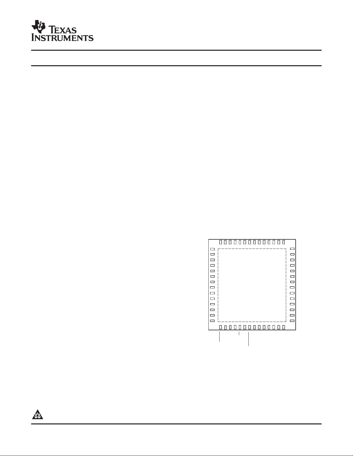
QFN56-Pin,8x8mmPackage
(TopView-NotToScale)
TPS65810
www.ti.com
SLVS658B – MARCH 2006 – REVISED FEBRUARY 2007
TPS65811
SINGLE-CELL Li-ION BATTERY- AND POWER-MANAGEMENT IC
1
FEATURES
• BATTERY CHARGER – 8-channel integrated A/D samples system
– Complete charge management solution for
single Li-Ion/Li-Pol cell with thermal
foldback, dynamic power management and • HOST INTERFACE
pack temperature sensing, supporting up
to 1.5-A max charge current
– Programmable charge parameters for AC
adapter and USB port operation
• INTEGRATED POWER SUPPLIES modification to host
– A total of 9 LDOs are integrated: – 3 GPIO ports, programmable as drivers,
– Six adjustable output LDOs (1.25-V to
3.3-V)
– Two fixed-voltage LDOs (3.3-V)
– One RTC backup supply with low
leakage (1.5-V)
– Two 0.6-V to 3.4-V programmable dc/dc
buck converters (600-mA for TPS65810,
750-mA for TPS65811) with enable,
standby-mode operation, and automatic
low-power mode setting
• DISPLAY FUNCTIONS
– Two open-drain PWM outputs with
programmable frequency and duty cycle.
Can be used to control keyboard backlight,
vibrator, or other external peripheral
functions
– RGB LED driver with programmable
flashing period and individual R/G/B
brightness control
– Constant-current white LED driver, with
programmable current level, brightness
control, and overvoltage protection can
drive up to 6 LEDs in series configuration
• SYSTEM MANAGEMENT
– Dual input power path function with input
– POR function with programmable masking
1
PRODUCTION DATA information is current as of publication date.
Products conform to specifications per the terms of the Texas
Instruments standard warranty. Production processing does not
necessarily include testing of all parameters.
current limiting and OVP protection
monitors all integrated supplies outputs
Please be aware that an important notice concerning availability, standard warranty, and use in critical applications of
Texas Instruments semiconductor products and disclaimers thereto appears at the end of this data sheet.
– Software and hardware reset functions
parameters with single conversion, peak
detection, or averaging operating modes
– Host can set system parameters and
access system status using I2C interface
– Interrupt function with programmable
masking signals system status
integrated A/D trigger or buck converters
standby mode control
APPLICATIONS
• PDAs
• Smart Phones
• MP3s
• Internet Appliances
• Handheld Devices
Copyright © 2006 – 2007, Texas Instruments Incorporated

www.ti.com
TPS65810
TPS65811
SLVS658B – MARCH 2006 – REVISED FEBRUARY 2007
This integrated circuit can be damaged by ESD. Texas Instruments recommends that all integrated circuits be handled with
appropriate precautions. Failure to observe proper handling and installation procedures can cause damage.
ESD damage can range from subtle performance degradation to complete device failure. Precision integrated circuits may be more
susceptible to damage because very small parametric changes could cause the device not to meet its published specifications.
DESCRIPTION
The TPS65810 provides an easy to use, fully integrated solution for handheld devices, integrating charge
management, multiple regulated power supplies, system management and display functions, in a small
thermally-enhanced 8x8 package. The high level of integration enables typical board area space savings of 70%
when compared to equivalent discrete solutions, while implementing a high-performance and flexible solution,
portable across multiple platforms. If required, an external host may control the TPS65810 via I2C interface, with
access to all integrated systems. The I2C enables setting output voltages, current thresholds, and operation
modes. Internal registers have a complete set of status information, enabling easy diagnostics, and
host-controlled handling of fault conditions. The TPS65810 can operate in stand-alone mode, with no external
host control, if the internal power-up defaults are compatible with the system requirements
AVAILABLE OPTIONS
T
J
– 40 ° C to 125 ° C TPS65810RTQ TPS65810
– 40 ° C to 125 ° C TPS65811RTQ TPS65811
(1) For the most current package and ordering information, see the Package Option Addendum at the end
of this document, or see the TI Web site at www.ti.com .
(2) The RTQ package is available in tape and reel. Add R suffix (TPS65810RTQR) to order quantities of
2000 parts per reel. Add T suffix (TPS65810RTQT) to order quantities of 250 parts per reel.
(3) This product is RoHS compatible, including a lead concentration that does not exceed 0.1% of total
product weight, and is suitable for use in specified lead-free soldering processes. In addition, this
product uses package materials that do not contain halogens, including bromine (Br) or antimony (Sb)
above 0.1% of total product weight.
(4) Other power-up sequences and default power-up states for the supplies can be implemented upon
request. Consult factory for available options
DEVICES
(2) (3) (4)
(1)
MARKING
2 Submit Documentation Feedback Copyright © 2006 – 2007, Texas Instruments Incorporated
Product Folder Link(s): TPS65810 TPS65811
www.ti.com
RTC_OUT
AC
BAT
OUT
USB
TMR
ISET1
TS
I2CINTERFACE
ANDINTERRUPT
CONTROLLER
INT
SDAT
SCLK
RESET
CONTROLLER
HOT_RST
RESPWRON
TRSTPWON
L1
PGND1
SM2
L2
L3
SM3
SIM
RED
BLUE
GREEN
SYS_IN
1.25V-3.3V
150 mA
LDO1
1.25V-3.3V
150 mA
LDO2
LDO3
1.224V-4.4V
100 mA
VIN_LDO35
1.224V-4.4V
100 mA
LDO4
LDO35_REF
ANLG1
ANLG2
GPIO1
GPIO2
3.3V
10 mA
LDO_PM
FB3
BAT
OUT
ADC_REF
GPIO3
AGND2
PGND3
VIN_SM1
VIN_SM2
PGND2
VIN_LDO2
DPPM
PWM
1.224V-4.4V
100 mA
LDO5
AGND1
LED_PWM
3.3V
150 mA
LDO0
AGND0
LDO3,4 ,5
LDO0,1,2
CONTROL
LOGIC
PWM
DRIVER
RGB
DRIVER
WHITELED
DRIVER
DISPLAY ANDI /O
GPIO’S
OUT
SM1
8 CHANNEL
MUX
A/D
CONVERTER
6 INTERNAL
CHANNELS
SM3_SW
1.5V
8 mA
1.8V/2.5V
8 mA
POWERPATH
CONTROL
LINEAR
CHARGER
0.6-1.8V
600 mA
1.0V-3.4V
600 mA
LDO_PM
CHARGE
MANAGEMENT
DC/DC
HOSTINTERFACE AND
SEQUENCING
ADC
AGND2
REFERENCE
SYSTEM
INTERNAL BIAS
OUT
OUT
OUT
TPS65810
SIM,RTCLDOS
SYSTEM
POWER
ON/OFF
OUT
AGND1AGND1
AGND1
OUT
AGND1
AGND1
AGND1
OUT
AGND1
BAT
AGND1
AGND 0,AGND 1 AND AGND 2PINSSHORTEDTOEACHOTHERINSIDETPS 65800. ALL AGNDPINS AREINTERNALLY CONNECTEDTO
THETPS 65800 THERMAL PAD ANDSUBSTRATE .
PGND1 ,PGND 3 ANDPGND 3PINS ARENOTCONNECTEDTOEACHOTHERORTOTHETPS
65800 SUBSTRATE / POWERPAD
DISPLAY ANDI /O
OUT
TPS65810
TPS65811
SLVS658B – MARCH 2006 – REVISED FEBRUARY 2007
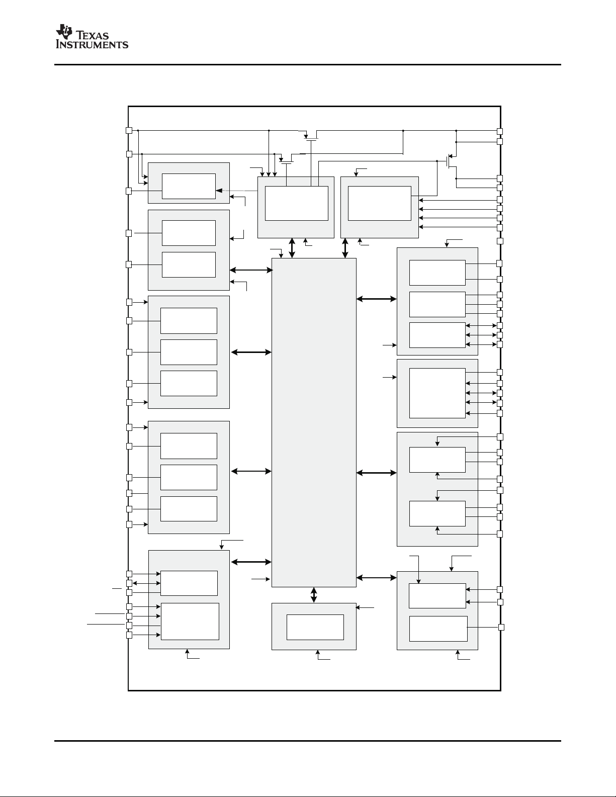
FUNCTIONAL BLOCK DIAGRAM
Copyright © 2006 – 2007, Texas Instruments Incorporated Submit Documentation Feedback 3
Figure 1. TPS65810 Simplified Block Diagram
Product Folder Link(s): TPS65810 TPS65811
www.ti.com
TPS65810
TPS65811
SLVS658B – MARCH 2006 – REVISED FEBRUARY 2007
ABSOLUTE MAXIMUM RATINGS
over operating free-air temperature range (unless otherwise noted)
AC and USB with respect to AGND1 – 0.3 to 18
ANLG1, ANLG2 with respect to AGND2 – 0.3 to V(OUT)
V(OUT) with respect to AGND1 5
VIN_LDO12, VIN_LDO35, LDO3, LDO4, LDO5 with respect to AGND2 – 0.3 to V(OUT)
LDO35_REF, ADC_REF with respect to AGND2 – 0.3 to smaller of: 3.6 or V(OUT)
SIM, RTC_OUT with respect to AGND1 – 0.3 to smaller of: 3.6 or V(OUT)
SM1, L1, VIN_SM1 with respect to PGND1 – 0.3 to V(OUT) V
SM2, L2, VIN_SM2 with respect to PGND2 – 0.3 to V(OUT)
SM3, L3 with respect to PGND3 – 0.3 to 29
SM3SW with respect to PGND3 – 0.3 to V(OUT)
FB3 with respect to PGND3 – 0.3 to 0.5
All other pins (except AGND and PGND), with respect to AGND1 – 0.3 to V(OUT)
AGND2, AGND0, PGND1, PGND2, PGND3 with respect to AGND1 – 0.3 to +0.3
Input Current, AC pin 2750
Input Current, USB pin 600
Output continuous current, OUT pin 3000 mA
Output continuous current, BAT pin – 3000
Continuous Current at L1, PGND1, L2, PGND2 1800
T
T
T
(1) Stresses beyond those listed under absolute maximum ratings may cause permanent damage to the device. These are stress ratings
Operating free-air temperature – 40 to 85
A
Maximum junction temperature 125
J
Storage temperature – 65 to 150
STG
Lead temperature 1,6 mm (1/16-inch) from case for 10 seconds 260
ESD rating, all pins 1.5 kV
only and functional operation of the device at these or any other conditions beyond those indicated under recommended operating
conditions is not implied. Exposure to absolute-maximum-rated conditions for extended periods may affect device reliability.
(1)
.
VALUE UNIT
° C
DISSIPATION RATINGS
PACKAGE θ
(1) (2)
RTQ
(1) This data is based on using the JEDEC High-K board and the exposed die pad is connected to a Cu
pad on the board. This is connected to the ground plane by a via matrix.
(2) The RTQ package MSL level: HIR3 at 260 ° C
4 Submit Documentation Feedback Copyright © 2006 – 2007, Texas Instruments Incorporated
JA
21.7 ° C/W 3.22 W 0.046 W/ ° C
Product Folder Link(s): TPS65810 TPS65811
TA≤ 55 ° C DERATING FACTOR
POWER RATING ABOVE TA= 55 ° C
www.ti.com
RECOMMENDED OPERATING CONDITIONS
AC and USB with respect to AGND1 4.35 16.5
ANLG1,ANLG2 with respect to AGND2 0 2.6 V
VIN_LDO35 with respect to AGND2 Greater of: 3.6 V OR minimum input 4.7
VIN_LDO12 with respect to AGND1 4.7
VIN_SM1 with respect to PGND1 4.7
VIN_SM2 with respect to PGND2 4.7
SM3 with respect to PGND3 28 V
T
A
T
J(op)
T
J
(1) Thermal operating restrictions are reduced or avoided if input voltage does not exceed 5 V.
Operating free-air temperature – 40 85 C
Junction temperature, functional operation assured – 40 125 C
Junction temperature, electrical characteristics assured 0 125 C
voltage required for LDO/converter
operation outside dropout region
TPS65810
TPS65811
SLVS658B – MARCH 2006 – REVISED FEBRUARY 2007
MIN MAX UNIT
(1)
V
V
Copyright © 2006 – 2007, Texas Instruments Incorporated Submit Documentation Feedback 5
Product Folder Link(s): TPS65810 TPS65811
www.ti.com
t
su(STOP)
t
(BUF)
STOP
START
1
9873
2
1
9873
2
ACK
ACK
SCL
SCL
SDA
SDA
t
su(STA)
START
t
r
STOP
t
h(STA)
t
h(DAT)
t
su(DAT)
SCL
SDA
t
w(H)
t
w(L)
t
f
t
r
t
f
t
h(DAT)
TPS65810
TPS65811
SLVS658B – MARCH 2006 – REVISED FEBRUARY 2007
ELECTRICAL CHARACTERISTICS – I2C INTERFACE
Over recommended operating conditions (typical values at TJ= 25 ° C), application circuit as in Figure 3 (unless otherwise
noted).
PARAMETER TEST CONDITIONS MIN TYP MAX UNIT
I2C TIMING CHARACTERISTICS
t
R
t
F
t
W(H)
t
W(L)
t
SU(STA)
t
H(STA)
t
SU(DAT)
t
H(DAT)
t
SU(STOP)
t
(BUF)
FSCL Clock Frequency 400 kHz
I2C INTERFACE LOGIC LEVELS
V
IH
V
IL
I
H
SCLK/SDATA rise time 300
SCLK/SDATA fall time 300 ns
SCLK pulse width high 600
SCLK Pulse Width Low 1.3 µ s
Setup time for START condition 600
START condition hold time after which first clock pulse is generated 600
Data setup time 100 ns
Data hold time 0
Setup time for STOP condition 600
Bus free time between START and STOP condition 1.3 µ s
High level input voltage 1.3 6
Low level input voltage 0 0.6
Input bias current 0.01 µ A
V
6 Submit Documentation Feedback Copyright © 2006 – 2007, Texas Instruments Incorporated
Figure 2. I2C Timing
Product Folder Link(s): TPS65810 TPS65811
www.ti.com
SLVS658B – MARCH 2006 – REVISED FEBRUARY 2007
ELECTRICAL CHARACTERISTICS – SYSTEM SEQUENCING AND OPERATING MODES
Over recommended operating conditions (typical values at TJ= 25 ° C), application circuit as in Figure 3 (unless otherwise
noted).
PARAMETER TEST CONDITIONS MIN TYP MAX UNIT
QUIESCENT CURRENT
I
BAT(SLEEP)
I
BAT(DONE)
I
BAT(CHGOFF)
I
INP(CHGOFF)
UNDERVOLTAGE LOCKOUT
V
UVLO
V
UVLO_HYS
t
DGL(UVLO)
SYSTEM LOW VOLTAGE THRESHOLD
V
LOW_SYS
V
HYS(LOWSYS)
t
DGL(LOWSYS)
THERMAL FAULT
T
SHUT
T
HYS(SHUT)
INTEGRATED SUPPLY POWER FAULT DETECTION
V
PGOOD
V
HYS(PGOOD)
HOT RESET FUNCTION
V
HRSTON
V
HRSTOFF
t
DGL(HOTRST)
SYSTEM RESET – OPEN DRAIN OUTPUT RESPWRON
V
RSTLO
I
TRSTPWON
K
RESET
BAT pin current, sleep
mode set
Input power not detected, V(BAT) = 4.2 V, Sleep mode set 400 µ A
BAT pin current, charge Charger function enabled by I2C, termination detected, input
terminated power detected and selected
BAT pin current, charge Charger function disabled by I2C, termination not detected,
function OFF input power detected and selected
AC or USB pin current,
charge function OFF
Internal UVLO detection NO POWER mode set at V(OUT) < V
threshold V(OUT) decreasing
UVLO detection
hysteresis
UVLO detection deglitch
time
Minimum system voltage System voltage V(SYS_IN) decreasing, SLEEP mode set if
detection threshold V(SYS_IN) < V
Minimum system voltage
detection hysteresis
Charger function disabled by I2C, termination not detected,
input power detected and selected. All integrated supplies 200 µ A
and drivers OFF, no load at OUT pin.
,
UVLO
– 3% 2.5 3% V
V(OUT) increasing 120 mV
Falling voltage only 5 ms
LOW_SYS
0.97 1 1.03 V
V(SYS_IN) increasing 50 mV
Minimum system voltage V(SYS_IN) decreasing
detection deglitch time
Thermal shutdown Increasing junction temperature 165 ° C
Thermal shutdown
hysteresis
Power good fault Falling output voltage, applies to all integrated supply outputs.
detection threshold Referenced to the programmed output voltage value
Power good fault Rising output voltage, applies to all integrated supply outputs.
detection hysteresis Referenced to V
Low level input voltage RESET mode set at V( HOT_RESET) < V
High level input voltage HOT reset not active at V( HOT_RESET) > V
Decreasing junction temperature 30 ° C
84% 90% 96%
threshold
PGOOD
HRSTON
HRSTOFF
3% 5% 7%
1.3 V
Hot reset input deglitch 5 ms
Low level output voltage IIL= 10 mA, V( RESPWRON ) < V
RSTLO
Pull-up current source Internally connected to TRSTPWRON pin 0.9 1.0 1.2 µ A
Reset timer constant T
= K
RESET
× C
RESET
TRSTPWON
TPS65810
TPS65811
3 µ A
3 µ A
5 ms
0.4 V
0 0.3 V
1 ms/nF
Copyright © 2006 – 2007, Texas Instruments Incorporated Submit Documentation Feedback 7
Product Folder Link(s): TPS65810 TPS65811
www.ti.com
TPS65810
TPS65811
SLVS658B – MARCH 2006 – REVISED FEBRUARY 2007
ELECTRICAL CHARACTERISTICS – POWER PATH AND CHARGE MANAGEMENT
Over recommended operating conditions (typical values at TJ= 25 ° C), circuit as in Figure 3 (unless otherwise noted).
PARAMETER TEST CONDITIONS MIN TYP MAX UNIT
VOLTAGE DETECTION THRESHOLDS
V
IN(DT)
V
IN(NDT)
t
DGL(NDT)
V
SUP(DT)
V
SUP(NDT)
Input Voltage detection AC detected at V(AC) – V(BAT) > V
threshold USB detected at V(USB) – V(BAT) > V
Input Voltage removal AC not detected at V(AC) – V(BAT) < V
threshold USB not detected at V(USB) – V(BAT) < V
Power not detected deglitch 22.5 ms
Supplement detection
threshold
Supplement not detected
threshold
POWER PATH INTEGRATED MOSFETs CHARACTERISTICS
V
ACDO
V
USBDO
V
BATDODCH
V
BATDOCH
AC switch dropout voltage 350 375 mV
USB switch dropout voltage
Battery switch dropout
voltage, discharge
Battery switch dropout Charger on, V(BAT): 3 V → 4.2 V, I(BAT) = 1 A 60 100 mV
voltage, charge
POWER PATH INPUT CURRENT LIMIT
I
INP(LIM1)
I
INP(LIM2)
Selected input current limit,
applies to USB input only
Selected Input current limit,
applies to USB input only
Selected Input current limit,
I
INP(LIM3)
applies to either AC or USB 2.75 A
input
SYSTEM REGULATION VOLTAGE
V
SYS(REG)
Output regulation voltage 4.6 4.7 V
POWER PATH PROTECTION AND RECOVERY FUNCTIONS
V
INOUTSH
R
SH(USBSH)
R
SH(ACSH)
Input-to-output short-circuit
detection threshold
OUT short circuit recovery
pullup resistor
OUT short circuit recovery
pullup resistor
Overvoltage detection Rising voltage, overvoltage detected when V(AC) > V
V
OVP
threshold V(USB) > V
Overvoltage detection
hysteresis
V
BATOUTSH
K
BLK(SHBAT)
I
SH(BAT)
R
SH(BAT)
R
DCH(BAT)
Battery-to-output short-circuit
detection threshold
Battery-to-ouput short-circuit V(DPPM) < 1v, t
blanking time constant connected from DPPM pin to AGND1
OUT short circuit recovery V
pullup current source Internal current source connected between OUT and BAT
BAT short circuit recovery V
resistor Internal resistor connected from OUT to BAT
BAT pulldown resistor 500 Ω
Battery switch ON at V(BAT) – V(OUT) > V
Battery switch OFF at V(BAT) – V(OUT) < V
V
= V(AC) – V(OUT); V(AC) = 4.75 V AC input current limit set to 2.75 A
ACDO
(typ), I
V
USBDO
USB input current limit set to 2.75 A (typ)
V(BAT): 3 V → V
= 1.0 A
O(OUT)
= V(USB) – V(OUT); V(USB) = 4.6 V I(OUT)+ I(BAT)= 0.5 A 175 190 mV
, I(BAT) = – 1 A 60 100 mV
CH(REG)
Selected input switch not in dropout, I2C settings: ISET2 = LO, PSEL = LO
Selected input switch not in dropout, I2C settings: ISET2 = HI, PSEL = LO
Selected input switch not in dropout, I2C settings: ISET2 = HI OR LO, PSEL
= HI
V
reached. Selected input voltage (AC or USB) > 5.1 V
= V(OUT), DPPM loop not active, selected input current limit not
SYS(REG)
AC and USB switches set to OFF if V(OUT) < V
V(OUT) < 1 V, internal resistor connected from USB to OUT 500 Ω
V(OUT) < 1 V, internal resistor connected from AC to OUT 500 Ω
OVP
Falling voltage, relative to detection threshold 0.1
BAT switch set to OFF if V(BAT) – V(OUT) > V
BLK(SHBAT)
– V
(BAT)
(BAT)
> V
(OUT)
< 1V,
= K
BLK(SHBAT)
,
BATOUTSH
Internal resistor connected from BAT to AGND1 when battery is not detected
by ANLG1
;
IN(DT)
IN(DT)
;
IN(NDT)
IN(NDT)
SUP(DT)
SUP(NDT)
190 mV
I(OUT)+ I(BAT)= 0.1 A 35 45 mV
400 500 mA
INOUTSH
or
OVP
BATOUTSH
X C
C
DPPM
capacitor is
DPPM,
125 mV
60 mV
20 mV
80 100 mA
0.6 V
6 6.5 6.8
V
200 mV
1 mS/nF
10 mA
1 k Ω
8 Submit Documentation Feedback Copyright © 2006 – 2007, Texas Instruments Incorporated
Product Folder Link(s): TPS65810 TPS65811
www.ti.com
V(OUT)* 1.2
500 kW
I
O(BAT)
+
K
(SET)
V
(SET)
R
SET
I
O(PRECHG)
+
V
(PRECHG)
K
(SET)
R
SET
I
(TERM)
+
V
(TERM)
K
(SET)
R
SET
SLVS658B – MARCH 2006 – REVISED FEBRUARY 2007
ELECTRICAL CHARACTERISTICS – POWER PATH AND CHARGE MANAGEMENT (Continued)
Over recommended operating conditions (typical values at TJ= 25 ° C), application circuit as in Figure 3 (unless otherwise
noted).
PARAMETER TEST CONDITIONS MIN TYP MAX UNIT
POWER PATH TIMING CHARACTERISTICS, DPPM AND THERMAL LOOPS NOT ACTIVE, R
t
BOOT
t
SW(ACBAT)
t
SW(USBBAT)
t
SW(PSEL)
t
SW(ACUSB)
Boot-up time Measured from input power detection 120 200 300 ms
Switching from AC to BAT 50 µ s
Switching from USB to BAT
Switching from USB to AC
Switching from AC to USB or USB to
AC
No USB: measured from V(AC) – V(BAT) < V
detected:CE=LO (after CE hold-off time)
No AC: measured from V(USB) – V(BAT) < V
detected:CE=LO (after CE hold-off time)
Toggling I2C PSEL bit
AC power removed or USB power removed 100 µ s
BATTERY REMOVAL DETECTION
V
NOBATID
t
DGL(NOBAT)
Battery ID resistor detection ID resistor not detected at V(OUT) – V(ANLG1) < V
Deglitch time for battery removal
detection
= 50 k Ω
TMR
, USB
IN(NDT)
,USB 50 µ s
IN(NDT)
NOBATID
TPS65810
TPS65811
50 µ s
0.5 V
0.6 1.2 ms
Set via I2C bits
I
O(ANLG1)
ANLG1 pullup current
(BATID1,BATID2)
ADC_WAIT register
Total accuracy 25% 25%
FAST CHARGE CURRENT, V(OUT) > V(BAT) + 0.1 V, V(BAT) > V
Charge current range 100 1500 mA
I
O(BAT)
V
= V(ISET1),
V
SET
K
SET
Battery charge current set voltage V
Battery charge current set factor
PRE-CHARGE CURRENT, V(OUT) > V(BAT) + 0.1 V, V
I
O(PRECHG)
V
PRECHG
V
LOWV
t
DGL(PRE)
Precharge current range 10 150 mA
Precharge set voltage V
Precharge to fast-charge transition Fast charge at V(BAT) > V
Deglitch time for fast charge to Decreasing battery voltage, R
precharge transition
CHARGE REGULATION VOLTAGE, V(OUT) > V
SET
(ISET1_1, ISET1_0) =
100 mA < I
1 mA < I
BATSH
PRECHG
+ 0.1V
O(BATREG)
Voltage options, selection via I2C
V
O(BATREG)
Battery charge voltage
Accuracy, TA= 25 ° C – 0.5% 0.5%
Total accuracy – 1% 1%
CHARGE TERMINATION, V(BAT) > V
, VOLTAGE REGULATION MODE SET
RCH
00, V
: 2.5 V to 4.4 V
(OUT)
01 10
10 50
11 60
LOWV
11, 100% scaling 2.475 2.500 2.525
10, 75% scaling 1.875 1.900 1.925
01, 50% scaling 1.225 1.250 1.275
00, 25% scaling 0.575 0.600 0.625
≤ 1 A 350 400 450
O(BAT)
≤ 100 mA 100 400 1000
O(BAT)
< V(BAT) < V
, t < t
LOWV
(PRECHG)
= V(ISET1) 220 250 270 mV
LOWV
= 50 k Ω 22.5 ms
TMR
2.8 3 3.2 V
4.2 V
4.356 V
µ A
I
TERM
Charge termination current range 10 150 mA
11, 100% scaling 240 260 280
V
TERM
Battery termination detection set V
voltage (ISET1_1, SET1_0) =
= V(ISET1),
TERM
10, 75% scaling 145 160 175
01, 50% scaling 90 110 130
00, 25% scaling 40 60 75
t
DGL(TERM)
Deglitch time for termination detection V(ISET1) < V
, R
TERM
= 50 k Ω 22.5 ms
TMR
Copyright © 2006 – 2007, Texas Instruments Incorporated Submit Documentation Feedback 9
Product Folder Link(s): TPS65810 TPS65811
mV

www.ti.com
TPS65810
TPS65811
SLVS658B – MARCH 2006 – REVISED FEBRUARY 2007
ELECTRICAL CHARACTERISTICS – POWER PATH AND CHARGE MANAGEMENT (Continued)
Over recommended operating conditions (typical values at TJ= 25 ° C), circuit as in Figure 3 (unless otherwise noted).
PARAMETER TEST CONDITIONS MIN TYP MAX UNIT
BATTERY RECHARGE DETECTION
V
RCH
t
DGL(RCH)
Recharge threshold voltage 80 100 130 mV
Deglitch time for recharge
detection
DPPM FUNCTION
V
DPPM
I
O(DPPM)
K
DPPM
t
DGL(DPPM
)
DPPM regulation point range V
DPPM pin current source AC or USB Present 95 100 105 µ A
DPPM scaling factor 1.139 1.15 1.162
DPPM de-glitch time 500 µ s
CHARGE AND PRE-CHARGE SAFETY TIMER
t
CHG
K
TMR
t
CHGADD
t
PRECHG
K
PRE
t
PCHGADD
R
TMR
R
TMR(FLT)
Charge safety timer Safety timer range, thermal/DPPM loop not active,
programmed value t
Charge timer set factor 0.313 0.36 0.414 s/ Ω
Total elapsed time when DPPM Fast charge on, t
or thermal loop are active t
Precharge safety timer Pre charge safety timer range, thermal/DPPM loop not active, min
programmed value t
Pre-charge timer set factor 0.09 0.1 0.11
Total elapsed time when DPPM Pre-charge on, t
or thermal loop are active t
External timer resistor limits 30 100 k Ω
Timer fault recovery pullup Internal resistor connected from OUT to BAT after safety timer
resistor timeout
THERMAL REGULATION LOOP
T
THREG
Temperature regulation limit Charge current decreased and timer extended when TJ> T
CHARGER THERMAL SHUTDOWN
T
THCHG
T
HCHGHYS
Charger thermal shutdown Charger turned off when TJ>T
Charger thermal shutdown
hystersis
New charge cycle starts if V(BAT) < V
termination was detected
R
= 50 k Ω 22.5 ms
TMR
= R
(DPPM)
× K
DPPM
× I
DPPMM
O(DPPM)
Status bit set indicating DPPM loop active after deglitch time,
R
= 50 k Ω
TMR
= R
CHG
CHG
PRECHG
PRECHG
× K
TMR
TMR
is the maximum add-on time added to
CHGADD
= K
× R
PRE
× K
TMR
TMR
is the maximum add-on time added to
PCHGADD
THCHG
– V
O(BATREG)
, after
RCH
2.6 4.4 V
3 5 10 h
18 30 60
2 × t
THREG
115 135 ° C
2 × t
CHG
PRECHG
150
1 k Ω
30
h
h
° C
10 Submit Documentation Feedback Copyright © 2006 – 2007, Texas Instruments Incorporated
Product Folder Link(s): TPS65810 TPS65811
www.ti.com
SLVS658B – MARCH 2006 – REVISED FEBRUARY 2007
ELECTRICAL CHARACTERISTICS – LINEAR REGULATORS
Over recommended operating conditions (typical values at TJ= 25 ° C), application circuit Figure 3 (unless otherwise noted).
PARAMETER TEST CONDITIONS MIN TYP MAX UNIT
SELECTABLE OUTPUT VOLTAGE LDO ’ S: LDO1, LDO2
I
= – 1 mA 15
I
Q(LDO12)
I
O(LDO1,2)
Quiescent current, either LDO1 or
LDO2 enabled, LDO0 disabled
I
Q(LDO12)
Output current range 150 mA
Output Voltage, Selectable via I2C.
Dropout voltage, 150 mA load 300 mV
V
O(LDO1,2)
LDO1, LDO2 Output Voltage Total accuracy, V(VIN_LDO02) = 3.65 V – 3% 3%
Line Regulation, 100 mA load,
V(VIN_LDO02): V
Load regulation, load: 10 mA → 150 mA
V(VIN_LDO02) > V
P
SR(LDO12)
I
SC(LDO1,2)
R
DCH(LDO1,2)
I
LKG(LDO1,2)
PSRR at 20 kHz 150mA load at output, V(VIN_LDO02) – V
LDO1&2 short circuit current limit Output grounded 300 mA
Discharge resistor 300 Ω
LDO disabled by I2C command
Leakage current LDO off 2 µ A
SIM LINEAR REGULATOR
I
Q(SIM)
I
O(SIM)
Quiescent current Internally connected to OUT pin 20 µ A
Output current range 8 mA
Output voltage, selectable via I2C.
Dropout voltage, 8 mA load 0.2 V
V
O(SIM)
SIM LDO output voltage
Total accuracy, V(OUT): 3.2 V to 4.7 V, 8 mA – 5% 5%
Load regulation, load: 1 mA → 8 mA,
V(OUT) > V
Line regulation, 5 mA load, V(OUT):
V
O(SIM) TYP
I
SC(SIM)
I
LKG(SIM)
Short-circuit current limit Output grounded 20 mA
Leakage current LDO off 1 µ A
PROGRAMMABLE OUTPUT VOLTAGE LDO ’ S: LDO3, LDO4, LDO5
I
Q(LDO35)
I
O(LDO35)
Quiescent current, only one of
LDO3, LDO4, LDO5 is enabled
I
Q(LDO35)
Output current range 100 mA
Output voltage, selectable via I2C
Dropout voltage, 100-mA load 240 mV
V
O(LDO35)
LDO3, LDO4, LDO5 output voltage Total accuracy, 100 mA load V
Load regulation, V(VIN_LDO35) > V
mA → 50 mA
Line regulation, 10-mA load,
V(VIN_LDO35): V
I
SC(LDO35)
PSR
(LDO35)
R
DCH(LDO35)
I
LKG(LDO35)
Short-circuit current limit Output grounded 250 mA
PSRR at 10 kHz V(VIN_LDO35) > V
Discharge resistor 400 Ω
LDO is disabled by I2C command
Leakage current LDO off 1 µ A
= I(VIN_LDO02) µ A
(LDO1,2)TYP
O(LDO1,2) TYP
+ 0.5 V
O(SIM) TYP
+ 0.5 V → 4.7 V
= I(VIN_LDO35) 70 µ A
O(LDO35)TYP
O(LDO3,5)
(LDO1,2)
I
= – 150 mA 160
(LDO1,2)
Available output voltages:
V
TYP = 1.25, 1.5, 1.8, V
O(LDO1,2)
2.5, 2.85, 3, 3.2, 3.3
+ 0.5 V → 4.7 V
+ 0.5V
=1V 40 dB
O(LDO1,2)
– 1% 1%
– 1.5% 1.5%
Available output voltages:
V
= 1.8 or 2.5
O(SIM)TYP
– 3% 3%
– 2% 2%
Available output voltages:
(VIN_LDO35)
O(LDO35)TYP
+ 0.5 V → 4.7 V
V
O(LDO35)TYP
4.46 V, 25-mV steps
= 5 V – 3% 3%
+ 0.5 V, load: 1
– 1% 1%
– 1% 1%
= 1.224 V to V
+1 V, 50 mA load at output 40 dB
TPS65810
TPS65811
V
ELECTRICAL CHARACTERISTICS – LINEAR REGULATORS (continued)
Over recommended operating conditions (typical values at TJ= 25 ° C), application circuit as in Figure 3 (unless otherwise
noted).
PARAMETER TEST CONDITIONS MIN TYP MAX UNIT
RTC_OUT LINEAR REGULATOR
Copyright © 2006 – 2007, Texas Instruments Incorporated Submit Documentation Feedback 11
Product Folder Link(s): TPS65810 TPS65811
www.ti.com
TPS65810
TPS65811
SLVS658B – MARCH 2006 – REVISED FEBRUARY 2007
ELECTRICAL CHARACTERISTICS – LINEAR REGULATORS (continued) (continued)
Over recommended operating conditions (typical values at TJ= 25 ° C), application circuit as in Figure 3 (unless otherwise
noted).
I
Q(RTC_OUT)
I
O(RTC_OUT)
V
O(RTC_OUT)
I
SH(RTC_OUT)
I
LKG(RTC_OUT)
LDO0 LINEAR REGULATOR
I
Q(LDO0)
I
O(LDO0)
V
O(LDO0)
PSR
I
SC(LDO0)
I
LKG(LDO0)
LDO_PM LINEAR REGULATOR
I
Q(LD0_PM)
V
O(LDO_PM)
I
LKG(LDOPM)
(LDO0)
Quiescent current for RTC LDO Internally connected to OUT pin 20 µ A
Output current range 8 mA
Fixed output voltage value 1.5 V
Dropout voltage, I(RTC_OUT) = – 8 mA 200 mV
RTC_OUT output voltage
Total accuracy, V(OUT): 2 V to 4.7 V, 8 mA load,
sleep mode not set
Load regulation, load: 1 mA → 8 mA,
2 V < V(OUT) < 4.7 V
Line regulation, 5-mA load
V(OUT): 2 V → 4.7 V
– 5% 5%
– 3% 3%
– 2% 2%
Short-circuit current limit V(RTC_OUT) = 0 V 20 mA
Leakage current nA
Quiescent current µ A
V(RTC_OUT) = 1.5 V,
V(OUT) = 0 V
Internally connected to VIN_LDO12
pin
TJ= 85 ° C 880
TJ= 25 ° C 250
I(LDO0) = – 1 mA 15
I(LDO0) = – 150 mA 160
Output current range 150 mA
Fixed output voltage value 3.3 V
Dropout voltage, I(LDO0) = – 150 mA 300 mV
Output voltage
Total accuracy – 3% 3%
Line regulation, V(OUT): V
I(LDO0) = – 100 mA
O(LDO0)
+ 0.5 → 4.7 V,
– 1% 1%
Load regulation, I(LDO0) = – 10 mA → – 150 mA – 1.5% 1.5%
PSRR at 20 kHz 150 mA load at output, V(VIN_LDO12) – V
= 1V 40 dB
O(LDO1,2)
Short circuit current limit V(LDO0) = 0 V 300 mA
Leakage current LDO off 1 µ A
Output current range 20 mA
Fixed output voltage value, V(OUT) > 4V 3.3 V
Output voltage Dropout voltage, I(LDOPM) = – 12 mA 0.5 0.7 V
Total accuracy – 5% 5%
Leakage current LDO off 1 µ A
12 Submit Documentation Feedback Copyright © 2006 – 2007, Texas Instruments Incorporated
Product Folder Link(s): TPS65810 TPS65811

www.ti.com
ELECTRICAL CHARACTERISTICS – SWITCHED-MODE SM1 STEP-DOWN CONVERTER
Over recommended operating conditions (typical values at TJ= 25 ° C), V
otherwise noted).
PARAMETER TEST CONDITIONS MIN TYP MAX UNIT
I
= I(VIN_ SM1), no output load Not switching 10
I
Q(SM1)
I
O(SM1)
V
O(SM1)
R
DSON(PSM1)
I
LKG(PSM1)
R
DSON(NSM1)
I
LKG(PSM1)
I
LIM(SM1)
f
S(SM1)
EFF
(SM1)
t
SS(SM1)
t
DLY(SM1)
Quiescent current for SM1 µ A
Output current range mA
Output voltage, PWM mode
P-channel MOSFET
on-resistance
P-channel leakage current 0.1 µ A
N-channel MOSFET
on-resistance
N-channel leakage current 5 µ A
P- and N-channel current limit mA
Oscillator frequency PWM mode set 1.3 1.5 1.7 MHz
Efficiency 90%
Soft start ramp time 750 µ s
Converter turn-on delay GPIO1 pin programmed as SM1 converter enable 170 µ s
Q(SM1)
SM1 OFF, set via I2C 0.1
Vin = 4.2 v, Vout = 1.24 V (TPS65810) 600
Vin = 4.2 v, Vout = 1.24 V (TPS65811) 750
Output voltage, selectable via I2C, Standby OFF 0.6 V to 1.8 V,
V
= V
O(SM1)
Total accuracy, V
V(VIN_SM1) = 3.0 V to 4.7 V; 0 mA ≤ I
, Output voltage range, Standby ON 0.6 V to 1.8 V,
SBY(SM1)
O(SM1)TYP
Line Regulation, V(VIN_SM1): 3.0 → 4.70 V, %/V
I
= 10 mA
O(SM1)
Load Regulation, V(VIN_SM1) = 4.7 V,
I
: 60 mA → 540 mA
O(SM1)
V(VIN_SM1) = 3.6 V, 100% duty cycle set 310 500 m Ω
V(VIN_SM1) = 3.6 V, 0% duty cycle set 220 330 m Ω
3 V < V(VIN_SM1) < 4.7 V (TPS65810) 900 1050 1200
3 V < V(VIN_SM1) < 4.7 V (TPS65811) 1000 1200 1400
V(VIN_SM1) = 4.2 V, PWM mode, I
V
= 3 V
O(SM1)
Converter OFF → ON, V
value
control. Measured from V(GPIO1): LO → HI
O(SM1)
O(SM1)
= V
SBY(SM1)
: 5% → 95% of target
O(SM1)
SLVS658B – MARCH 2006 – REVISED FEBRUARY 2007
= 1.24 V, application circuit Figure 3 (unless
Available output
= 1.24 V,
O(SM1)
= 300 mA,
≤ 600 mA
voltages: V
adjustable in 40-mV
voltages: V
adjustable in 40-mV
– 3% 3%
O(SM1)TYP
steps
Available output
SBY(SM1)
steps
0.027
0.139 %/A
TPS65810
TPS65811
=
V
=
Copyright © 2006 – 2007, Texas Instruments Incorporated Submit Documentation Feedback 13
Product Folder Link(s): TPS65810 TPS65811
www.ti.com
TPS65810
TPS65811
SLVS658B – MARCH 2006 – REVISED FEBRUARY 2007
ELECTRICAL CHARACTERISTICS – SWITCHED MODE SM2 STEP DOWN CONVERTER
Over recommended operating conditions (typical values at TJ= 25 ° C), V
otherwise noted).
PARAMETER TEST CONDITIONS MIN TYP MAX UNIT
I
= I(VIN_ SM2), no output load, not 10
Q(SM2)
I
Q(SM2)
I
O(SM2)
V
O(SM2)
R
DSON(PSM2)
I
LKG(PSM2)
R
DSON(NSM2)
I
LKG(PSM2)
I
LIM(SM2)
f
S(SM2)
EFF
(SM2)
t
SS(SM2)
t
DLY(SM2)
Quiescent current for SM2 µ A
Output current range mA
Output voltage V(VIN_SM2) = greater of [3.0 V or (V
P-channel MOSFET
on-resistance
P-channel leakage current 0.1 µ A
N-channel MOSFET
on-resistance
N-channel leakage current 5 µ A
P- and N-channel current limit mA
Oscillator frequency PWM mode set 1.3 1.5 1.7 MHz
Efficiency 90%
Soft start ramp time 750 µ s
Converter turn-on delay GPIO2 pin programmed as SM2 converter 170 µ s
switching
SM2 OFF, set via I2C 0.1
Vin = 4.2 v, Vout = 1.24 V (TPS65810) 600
Vin = 4.2 v, Vout = 1.24 V (TPS65811) 750
Output voltage, selectable via I2C, standby OFF V
V
= V
O(SM2)
Standby ON
Total accuracy, V
, Output voltage range,
SBY(SM2)
O(SM2)TYP
V)]
to 4.7 V; 0 mA ≤ I
O(SM2)
Line regulation, V(VIN_SM2) = greater of %/V
[3 V or (V
to 4.7 V; 0 mA ≤ I
+ 0.3 V)] 0.027
O(SM2)
O(SM2)
Load regulation, V(VIN_SM2) = 4.7 V,
I
: 60 mA → 540 mA
O(SM2)
V(VIN_SM2) = 3.6 V, 100% duty cycle set 310 500 m Ω
V(VIN_SM2) = 3.6 V, 0% duty cycle set 220 330 m Ω
3 V < V(VIN_SM2) < 4.7 V (TPS65810) 900 1050 1200
3 V < V(VIN_SM2) < 4.7 V (TPS65811) 1000 1200 1400
V(VIN_SM2) = 4.2 V, I
V
= 3 V
O(SM2)
Converter OFF → ON, V
target value
enable control. Measured from V(GPIO2): LO →
HI
≤ 600 mA
≤ 600 mA
O(SM2)
O(SM2)
O(SM1)
= V
SM2(SBY)
= 300 mA,
: 5% → 95% of
= 1.24 V, application circuit Figure 3 (unless
Available output voltages:
O(SM2)TYP
adjustable in 80-mV steps
Available output voltages:
V
SBY(SM2)
adjustable in 80-mV steps
= 1.8 V,
+ 0.3
O(SM2)
= 1 V to 3.4 V,
= 1 V to 3.4 V,
– 3% 3%
0.139 %/A
V
ELECTRICAL CHARACTERISTICS – GPIOs
Over recommended operating conditions (typical values at TJ= 25 ° C), application circuit as in Figure 3 (unless otherwise
noted).
PARAMETER TEST CONDITIONS MIN TYP MAX UNIT
GPIO1 – 3
V
OL
I
OGPIO
V
IL
I
LKG(GPIO)
14 Submit Documentation Feedback Copyright © 2006 – 2007, Texas Instruments Incorporated
Low level output voltage GPIO0 IOL= 20 mA 0.5 V
Low level sink current into GPIO1,2,3 V(GPIOn) = V(OUT) 20 mA
Low level input voltage 0.4 V
Input leakage current V(GPIOn) = V(OUT) 1 µ A
Product Folder Link(s): TPS65810 TPS65811
www.ti.com
V(OUT)* 1.2
500 kW
TPS65810
TPS65811
SLVS658B – MARCH 2006 – REVISED FEBRUARY 2007
ELECTRICAL CHARACTERISTICS – ADC
Over recommended operating conditions (typical values at TJ= 25 ° C), V(ADC_REF) =2.535v if external reference voltage is
used, application circuit as in Figure 3 (unless otherwise noted).
PARAMETER TEST CONDITIONS MIN TYP MAX UNIT
ANALOG INPUTS
V
RNG(CH1_5)
V
RNG(CH6_8)
C
IN(ADC)
R
INADC(CH1_5)
I
LKGADC(CH1_5)
R
INADC(CH6_8)
I
LKGADC(CH6_8)
V
CH5(ADC)
DC ACCURACY
RES
(ADC)
MCD
(ADC)
INL
(ADC)
DNL
(ADC)
OFF
ZERO(ADC)
OFF
CH(ADC)
GAIN
ADC
GAIN
CH(ADC)
THROUGHPUT SPEED
ADC
CLK
ADC
TCONV
REFERENCE VOLTAGES
V
INTREF
I
SHRT(INTREF)
V
REF(DRIFT)
I
Q(ADC)
I
(ANLG2)
Full scale input range Ch1 to Positive inputs (active clamp) V(ADC_
Ch5 Full scale ~ 2.535 V REF)
Full scale input range Ch6 to V
Ch8 × 1.854
Positive inputs (active clamp), full scale ~4.7 V 0 V
Input capacitance (all
channels)
0 V
INTREF
15 pF
Input resistance (Ch1 to Ch5) 1 M Ω
Leakage current (Ch1 to Ch5) 100 nA
Input resistance (Ch6 to Ch8) 430 540 k Ω
Leakage current (Ch6 to Ch8) 10 µ A
Internal voltage proportional to
junction temperature
TJ= 25 ° C, ADC channel 5 input voltage 1.895 V
Temperature coefficient 6.5 mV/ ° C
Resolution SAR ADC 10 Bits
No missing codes SPECIFIED
Integral linearity error ± 3 LSB
Differential non-linearity error ± 1 LSB
Offset error 5 LSB
Offset error match between
channels
Gain error ± 8 LSB
Difference between the first code transition
(00...00 to 00...01) and the ideal AGND + 1 LSB
5 LSB
Deviation in code from the ideal full scale code
(11 … 111) for the full scale voltage
Gain error match Any two channels 2 LSB
Sampling clock 600 750 900 kHz
Conversion time 44 59 68 µ s
Internal ADC reference TA= 25 ° C, V(ADC_REF)=V
voltage ADC reference is selected
Internal reference short circuit V(ADC_REF)= AGND1, internal reference
limit enabled via I2C
ADC internal reference
temperature drift
ADC Internal reference Measured at OUT pin (internal reference) or
quiescent current ADC_REF pin (external reference)
Sampling, conversion and setting Rs ≤ 200 K for
CH1,CH2,CH3; Rs ≤ 500 Ω for CH6, CH7, CH8
when internal
INTREF
2.53 2.535 2.54 V
6 mA
50 100 ppm/ ° C
40 µ A
00 0
ANLG2 pin internal pullup
current source
ADC channel 2 bias current, set via
I2C register ADC_WAIT bits µ A
(ADC_CH2I_D1_1, ADC_CH2I _D2)
01 10
10 50
11 60
Total accuracy, relative to selected value – 25% 25%
00 µ A
ADC channel 1 bias current, set via
I
(ANLG1)
ANLG1 pin internal pullup
current source
I2C register ADC_WAIT bits
(BATIDI_D1, BATIDI _D2)
01 10
10 50
11 60
Total accuracy 10% 10%
Copyright © 2006 – 2007, Texas Instruments Incorporated Submit Documentation Feedback 15
Product Folder Link(s): TPS65810 TPS65811
www.ti.com
I
O(SM3)
+
V(SM3REF)
R
FB3
TPS65810
TPS65811
SLVS658B – MARCH 2006 – REVISED FEBRUARY 2007
ELECTRICAL CHARACTERISTICS – ADC (continued)
Over recommended operating conditions (typical values at TJ= 25 ° C), V(ADC_REF) =2.535v if external reference voltage is
used, application circuit as in Figure 3 (unless otherwise noted).
PARAMETER TEST CONDITIONS MIN TYP MAX UNIT
INTERNAL REFERENCE POWER CONSUMPTION
PD
ACTIVE
PD
ARMED
TRIGGER TIMING CHARACTERISTICS
t
DELAY(TRG)
t
WAIT(TRG)
ELECTRICAL CHARACTERISTICS – LED AND PWM DRIVERS
Over recommended operating conditions (typical values at TJ= 25 ° C), application circuit as in Figure 3 (unless otherwise
noted).
SM3 BOOST CONVERTER, WHITE LED CONSTANT CURRENT DRIVER
V
VIN(SM3)
V
OVP3
V
HYS(OVP3)
V
SM3REF
Power dissipation Conversion active 2.3 mW
Power dissipation Not converting 0.43 mW
Trigger delay time accuracy Time range, set via I2C register ADC_DELAY 0 750 uS
Relative to typical value set via I2C – 20% +20%
Trigger wait time accuracy Time range, set via I2C register ADC_WAIT 0 20.48 mS
Relative to typical value set via I2C – 20% +20%
PARAMETER TEST CONDITIONS MIN TYP MAX UNIT
Input Voltage range V(OUT) = 3.3 V 3 4.7 V
Output overvoltage trip OVP detected at V(SM3) > V
Output overvoltage hysteresis OVP not detected at V(SM3) < V
LED current sense threshold 244 252 260 mV
LED current below regulation point at
V(FB3) < V
SM3REF
OVP3
– V
OVP3
HYS(OVP3)
26.5 29 30 V
1.8 V
I
O(SM3)
D
SM3SW
F
REP_SM3
R
DSON(SM3SW)
I
LKG(SM3SW)
R
DSON(L3)
I
LKG(L3)
I
MAX(L3)
LED current
LED switch duty cycle Duty cycle range –
LED switch duty cycle pattern 256 pulses within repetition
repetition rate rate time
LED switch MOSFET
on-resistance
LED switch MOSFET leakage 1 µ A
Power stage MOSFET
on-resistance
Power stage MOSFET
leakage
Power stage MOSFET current
limit
PWM DRIVER, PWM OPEN DRAIN OUTPUT
V
OL(PWM)
F
PWM
D
PWM
Low level output voltage I(PWM)= 150 mA 0.5 V
PWM driver frequency
PWM driver duty cycle Duty cycle range via I2C, –
Current range, Vin = 3.3 V,
Total accuracy, I
O(SM3)
= 10mA – 10% 10%
0 25 mA
D
SM3SW
= 0% to 99.6%, set
via I2C,
256 steps, 0.4% minimum
step
SM3_LF_OSC = 0 122
SM3_LF_OSC = 1 183
V(OUT)=3.6 V; I(SM3SW)=20 mA 1 2 Ω
V(OUT) = 3.6 V; I(L3) = 200 mA 300 600 m Ω
1 µ A
3 V < V(OUT) < 4.7 V 400 500 600 mA
Frequency range Hz
Set via I2C, F
0.5/1/1.5/2/3/4.5/7.8/15.6
=
PWM
Total accuracy, relative to selected value – 20% +20%
D
= 6.25% to 100%, set
PWM
6.25% minimum step
Hz
16 Submit Documentation Feedback Copyright © 2006 – 2007, Texas Instruments Incorporated
Product Folder Link(s): TPS65810 TPS65811
www.ti.com
SLVS658B – MARCH 2006 – REVISED FEBRUARY 2007
ELECTRICAL CHARACTERISTICS – LED AND PWM DRIVERS (continued)
Over recommended operating conditions (typical values at TJ= 25 ° C), application circuit as in Figure 3 (unless otherwise
noted).
PARAMETER TEST CONDITIONS MIN TYP MAX UNIT
LED_PWM DRIVER, LED_PWM OPEN DRAIN OUTPUT
D
D
LEDPWM
F
REP(LEDPWM)
V
OL(LEDPWM)
V
OH(LEDPWM)
LED_PWM driver duty cycle Duty cycle range set via I2C, 256 steps
LED_PWM driver duty cycle 256 pulses within repetition
pattern repetition rate rate time
Low level output voltage I(LED_PWM) = 150 mA 0.5 V
High level output voltage 6 V
RGB DRIVER, RED/GREEN/BLUE OPEN DRAIN OUTPUTS
t
FLASH(RGB)
t
FLASH(ON)
D
RGB
I
SINK(RGB)
V
OL(RGB)
I
LKG(RGB)
Flashing period
Flash on time
Duty cycle Duty cycle range, value selectable via I2C via I2C, 3.23% minimum
RGB output sink current V(BLUE) = 2 V, set via I2C mA
Low-level output voltage 0.3 V
Output off leakage current 1 µ A
SM3_LF_OSC = 0 122
SM3_LF_OSC = 1 180
Flashing period range via I2C, 0.5 sec minimum sec
Total accuracy – 20% +20%
Flash on time range, value selectable by I2C 0.1/0.15/0.2/0.25/0.3/0.4/ sec
Total accuracy relative to selected value – 20% +20%
00 = (Driver set to
V(RED) = V(GREEN) =
RGB_ISET1,0
OFF)
01 2.4 4 5.6
10 4.8 8 11.2
11 7 12 16.6
Output low voltage, 8-mA load, RED/GREEN/BLUE
PINS
V(RED)=V(GREEN)=V(BLUE) = 4.7 V, all drivers
disabled
LEDPWM
t
FLASH(RGB)
Set via I2C, t
D
RGB
0.4% minimum step
step, 8 steps
0.5/0.6 Sec
= 0% to 99.98%, set
= 0% to 99.6%,
= 1 to 8 sec, set
FLASH(ON)
TPS65810
TPS65811
Hz
=
step
Copyright © 2006 – 2007, Texas Instruments Incorporated Submit Documentation Feedback 17
Product Folder Link(s): TPS65810 TPS65811

www.ti.com
SYS_IN
L1
SM1
PGND1
PGND2
SM2
L2
AGND0
SM3
FB3
L3
SM3SW
OUT
SIM
OUT
GPIO1
USB
GPIO2
LDO_PM
PWM
AC
RED
BA T
GREEN
BA T
BLUE
TMR
SCLK
ISET1
SDA T
DPPM
INT
TS
RESPWRON
R TC_OUT
TRSTPWON
HOT_RST
LDO1
LDO0
LDO3
LDO35_REF
VIN_LDO35
LDO4
ADC_REF
AGND2
ANLG1
ANLG2
LDO5
GPIO3
GROUNDPAD
AGND1
VIN_LDO02
PGND3
VIN_SM2
VIN_SM1
2
11
8
13
10
12
9
6
7
5
3
4
14
38
41
36
39
37
40
42
34
35
33
32
31
30
27
29
25 282624232219 21201817
LED_PWM
LDO2
48 47 434446 4549505154 5256 5355
1
1615
TPS65810
TPS65811
SLVS658B – MARCH 2006 – REVISED FEBRUARY 2007
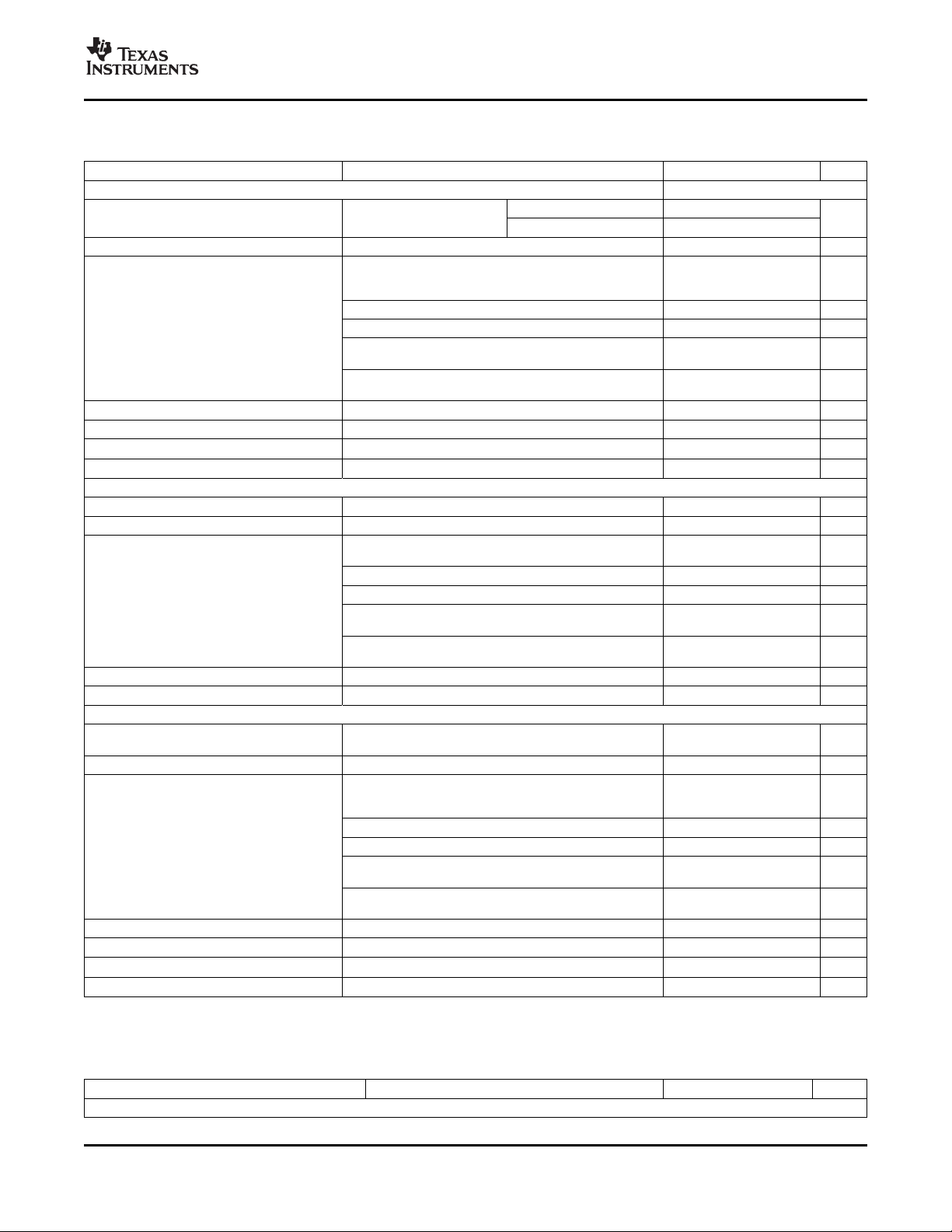
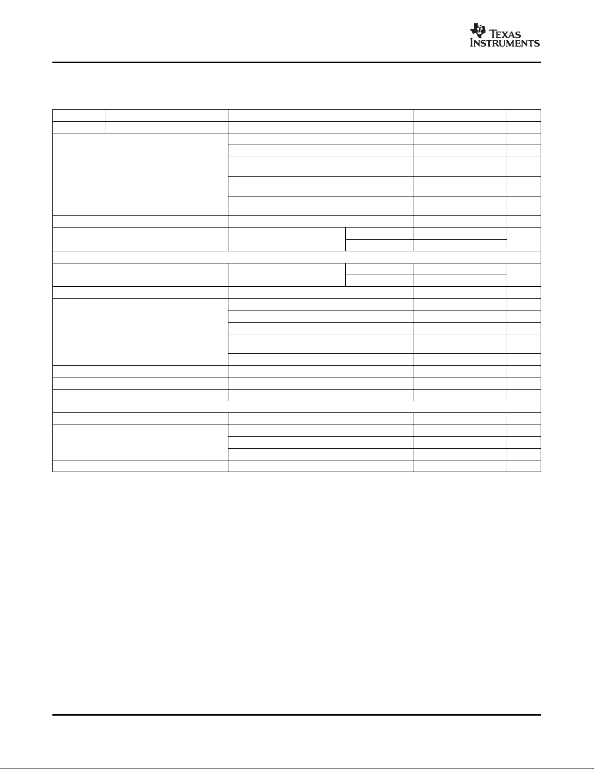
PIN ASSIGNMENT
PIN DESCRIPTION, REQUIRED EXTERNAL COMPONENTS
NAME PIN I/O DESCRIPTION EXTERNAL REQUIRED COMPONENTS
AC 7 I Adapter charge input voltage, connect to 1- µ F (minimum) capacitor to AGND1 pin to minimize
AC_DC adapter positive output terminal overvoltage transients during AC power hot-plug events.
(dc voltage)
ADC_REF 22 I/O ADC internal reference filter or ADC 4.7 µ F (minimum) to 10 µ F (maximum) capacitor connected to
external reference input AGND2 pin
AGND0 16 – Analog ground connection Connect to analog ground plane
AGND1 48 – Analog ground pin Connect to analog ground plane
AGND2 25 – Analog ground pin Connect to analog ground plane
ANLG1 24 I Analog input to ADC, programmable Can be used to monitor additional system or pack parameters
current source output
ANLG2 23 I Analog input to ADC, programmable Can be used to monitor additional system or pack parameters
current source output
BAT 17, I/O Battery power Connect to battery positive terminal. Connect 10- µ F capacitor
18 (minimum) from BAT pin to AGND1 pin.
BLUE 1 O Programmable blue driver, open drain Connect to BLUE input of RGB LED
DPPM 14 I Dynamic power path management External resistor from DPPM pin to AGND1 pin sets the DPPM
FB3 41 I/O White LED duty cycle switch output, LED External resistor from FB3 pin to PGND3 pin sets LED peak
GPIO1 43 I/O General purpose programmable I/O Power-up default: SM1 enable control, SM1 ON @ GPIO1=HI.
GPIO2 53 I/O General purpose programmable I/O Power-up default: SM2 enable control, SM2 ON at GPIO2 = HI.
GPIO3 54 I/O General purpose programmable I/O. Example: ADC conversion start trigger.
GREEN 56 O Programmable LED driver, open drain Connect to GREEN input of RGB LED
18 Submit Documentation Feedback Copyright © 2006 – 2007, Texas Instruments Incorporated
output, current sink output when active.
to AGND1 sets BAT to OUT short circuit blanking delay when
battery is hot-plugged into system
pin.
set-point regulation threshold. 1-nF (minimum) capacitor to from DPPM
current setting current. Connect 100 pF (minimum) filter capacitor to PGND3
output, current sink output when active.
Product Folder Link(s): TPS65810 TPS65811
(SEE APPLICATION DIAGRAM)

www.ti.com
TPS65810
TPS65811
SLVS658B – MARCH 2006 – REVISED FEBRUARY 2007
NAME PIN I/O DESCRIPTION EXTERNAL REQUIRED COMPONENTS
HOT_RST 15 I/O Hardware reset input, reset generated Connect to an external push-button switch. Connect to external
when connected to ground pullup resistor.
INT 19 O Interruption pin, open-drain output Connect 100-k Ω external pullup resistor between INT and OUT
INT pin is LO when interrupt is requested by TPS65810.
ISET1 11 I Current set point when charging in auto External resistor from ISET1 pin to AGND1 pin sets charge
mode with AC selected. Pre-charge and current value
charge termination set point for all charge
modes
L1 46 O SM1 synchronous buck converter 3.3- µ H inductor to SM1 pin
power-stage output
L2 51 O SM2 synchronous buck converter 3.3- µ H inductor to SM2 pin
power-stage output
L3 39 O Drain of the integrated boost power-stage 4.7- µ H inductor to OUT pin, external Schottky diode to SM3 pin
switch
LDO0 32 O LDO0 output, fixed voltage 1- µ F (minimum) capacitor to AGND1
LDO1 37 O LDO1 output 1- µ F (minimum) capacitor to AGND1
LDO2 33 O LDO2 output 1- µ F (minimum) capacitor to AGND1
LDO3 28 O LDO3 output 2.2- µ F (minimum) capacitor to AGND2
LDO35_REF 30 I Linear regulators LDO3-5 reference filter 100-nF capacitor to AGND2
LDO4 27 O LDO4 output 2.2- µ F (minimum) capacitor to AGND2
LDO5 26 O LDO5 output 2.2- µ F (minimum) capacitor to AGND2
LDO_PM 10 O General purpose LDO output 1- µ F (minimum) capacitor to AGND1 pin
LED_PWM 36 O PWM driver output, open drain. Can be used to drive a keyboard backlight LED
OUT 8, 9 O Power-path output. Connect to system 10- µ F capacitor to AGND1 pin
main power rail (system power bus)
PGND1 45 – SM1 synchronous buck converter power Connect to Power ground plane
ground
PGND2 52 – SM1 synchronous buck converter power Connect to power ground plane
ground
PGND3 38 – White LED driver power ground input. Connect to a power ground plane
PWM 34 O PWM driver output, open drain. Can be used to drive a vibrator or other external functions
RED 55 O Programmable LED driver, open drain Connect to RED input of RGB LED
output, current sink output when active.
RESPWRON 21 O System reset, open-drain output 100-k Ω external pullup resistor to OUT. RESPWRON pin is LO
when TPS65810 is resetting the system.
RTC_OUT 4 O Low leakage LDO output. Can be 1- µ F (minimum) capacitor to AGND1 pin or supercapacitor
connected to a super-capacitor or
secondary cell, if used as a RTC backup
output.
SCLK 2 I I2C interface clock line 2-k Ω pullup resistor to OUT pin
SDAT 3 I/O I2C interface data line 2-k Ω pullup resistor to OUT pin
SIM 5 O General purpose LDO output 1- µ F (minimum) capacitor to AGND1 pin
SM1 44 I SM1 synchronous buck converter output LC filter: 10- µ F capacitor to PGND1 pin
voltage sense
SM2 49 I SM2 synchronous buck converter output LC filter: 10- µ F capacitor to PGND2 pin
voltage sense
SM3 42 I White LED driver output overvoltage Connect 1- µ F capacitor to PGND3 pin. Connect SM3 pin to the
detection positive side of white LED ladder.
SM3SW 40 I Integrated white LED duty cycle switch Connect to negative side of external LED ladder
input
SYS_IN 31 I System power bus low-voltage detection External resistive divider sets minimum system operational
voltage. TPS65810 enters sleep mode when voltage below
minimum system voltage threshold is detected. 1-nF filter
capacitor to AGND1 recommended.
(SEE APPLICATION DIAGRAM)
Copyright © 2006 – 2007, Texas Instruments Incorporated Submit Documentation Feedback 19
Product Folder Link(s): TPS65810 TPS65811

www.ti.com
TPS65810
TPS65811
SLVS658B – MARCH 2006 – REVISED FEBRUARY 2007
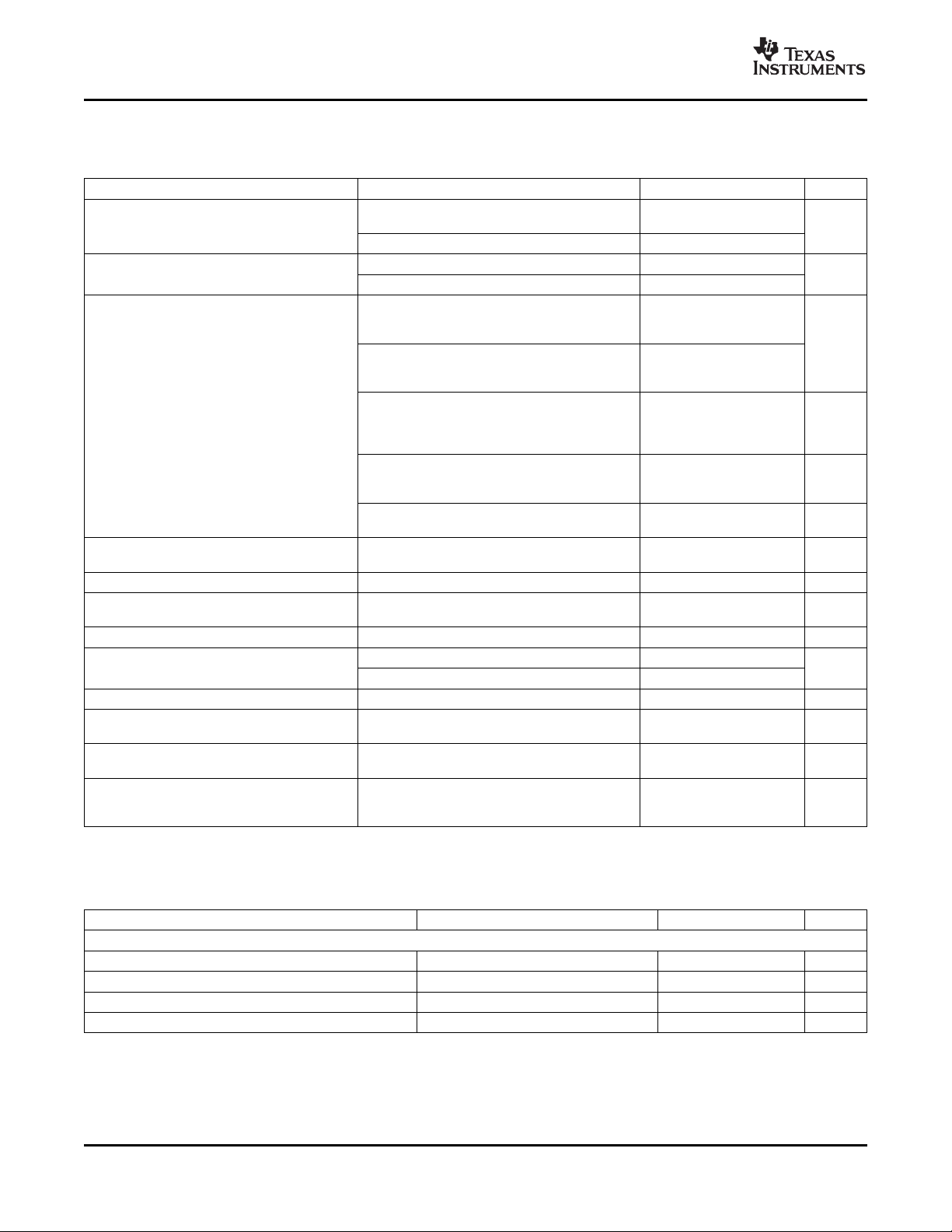
NAME PIN I/O DESCRIPTION EXTERNAL REQUIRED COMPONENTS
TMR 13 I Charge safety timer program input External resistor from TMR pin to AGND1 pin sets the charge
safety timer time-out value
TRSTPWON 20 I System reset pulse-duration setting 100-nF (minimum) capacitor to AGND. External capacitor from
TRSTPWON pin to AGND1 pin sets RESPWRON pulse
duration.
TS 12 I/O Temperature sense input, current source Connect to battery pack thermistor to sense battery pack
output temperature. Connect to external pullup resistor.
USB 6 I USB charge input voltage, connect to 1- µ F (minimum) capacitor to AGND1 pin, to minimize
USB port positive power output overvoltage transients during USB power hot-plug events.
VIN_LDO35 29 – Input to LDOs 3 to 5 1- µ F (minimum) decoupling capacitor to AGND2
VIN_LDO02 35 – Positive supply input for LDO0, LDO1, 1- µ F (minimum) decoupling capacitor to AGND1
LDO2
VIN_SM1 47 – SM1 synchronous buck converter positive 10- µ F capacitor to PGND1 pin
supply input
VIN_SM2 50 – SM2 synchronous buck converter positive 10- µ F capacitor to PGND2 pin
supply input
Exposed 57 – There is an internal electrical connection between the exposed thermal pad and AGNDn pins of the IC. The
thermal pad exposed thermal pad must be connected to the same potential as the AGND1 pin on the printed circuit
board. Do not use the thermal pad as the primary ground input for the IC. AGNDn pins must be connected
to a clean ground plane at all times.
(SEE APPLICATION DIAGRAM)
20 Submit Documentation Feedback Copyright © 2006 – 2007, Texas Instruments Incorporated
Product Folder Link(s): TPS65810 TPS65811
www.ti.com
SM 1
AC
BAT
OUT
USB
TMR
DPPM
TS
HOT _RST
L 1
SM 2
L 2
L 3
SM 3
SM 3SW
BAT
OUT
7
Battery
PGND 1
PGND 2
PGND 3
FB 3
VIN _ SM 2
VIN _SM 1
PWM
LED _PWM
RED
BLUE
GREEN
AGND 1
VIN _ LDO 12
LDO 1
LDO 0
LDO 2
TRSTPWON
SYS _ IN
TPS65810
INT
SDAT
SCLK
RESPWRON
AGND 2
EXTERNAL HOST
GPIO 2
GPIO 1
ANLG 1
GPIO 3
ANLG 2
ADC _REF
VIN _ LDO 35
LDO 35 _ REF
LDO 4
LDO 3
LDO 5
1 uF
2 .2 uF
A 1
0 .1 uF
1 nF
210 K
100 K
AC _ DC
ADAPTER
OUTPUT
USB
POWER
GND
GND
+
-
2 K
100 K
100 K
A 2
A 1
V LDO 2
V LDO 1
V LDO 0
V LDO 5
V LDO 4
V LDO 3
P 3
P 2
V SM2
V SM1
P 1
A 1
GND
49 . 9 K
37 .4 K
100 pF
GND
A 1 A 2 A 3
P 1 P 2
P 3
SIM
RTC _ OUT
AGND 0
A 0
V RTC_OUT
ISET 1
1 K
Supercap
LDO _ PM
V
LDO_PM
V
SIM
2 K
37
32
35
10
4
5
6
50
45
44
46
47
14
13
12
18
17
11
9
8
48
33
39
40
52
49
51
2
16
31
20
15
25
26
27
28
30
29
42
21
19
3
56
55
36
34
41
38
53
43
1
24
23
54
22
A 2
+
-
2 .2 uF
2 .2 uF
1 uF
4 .7 uF
4. 7uF
4 .7 uF
0 .1 uF
1 uF
10 uF
10 uF
2 .2 uF
1 uF
100 pF
4 .7 uH
10 uF
10 uF
10 uF
10 uF
3 .3 uH
3. 3uH
47 nF
10 uF
22 uF
0 .22 uF
4 .7 uF
SYSTEM
POWER
BUS
ADC
EXTERNAL
ANALOG
INPUTS
ADCTRIGGER
CLOCK
DATA
ALARM
RESET
10
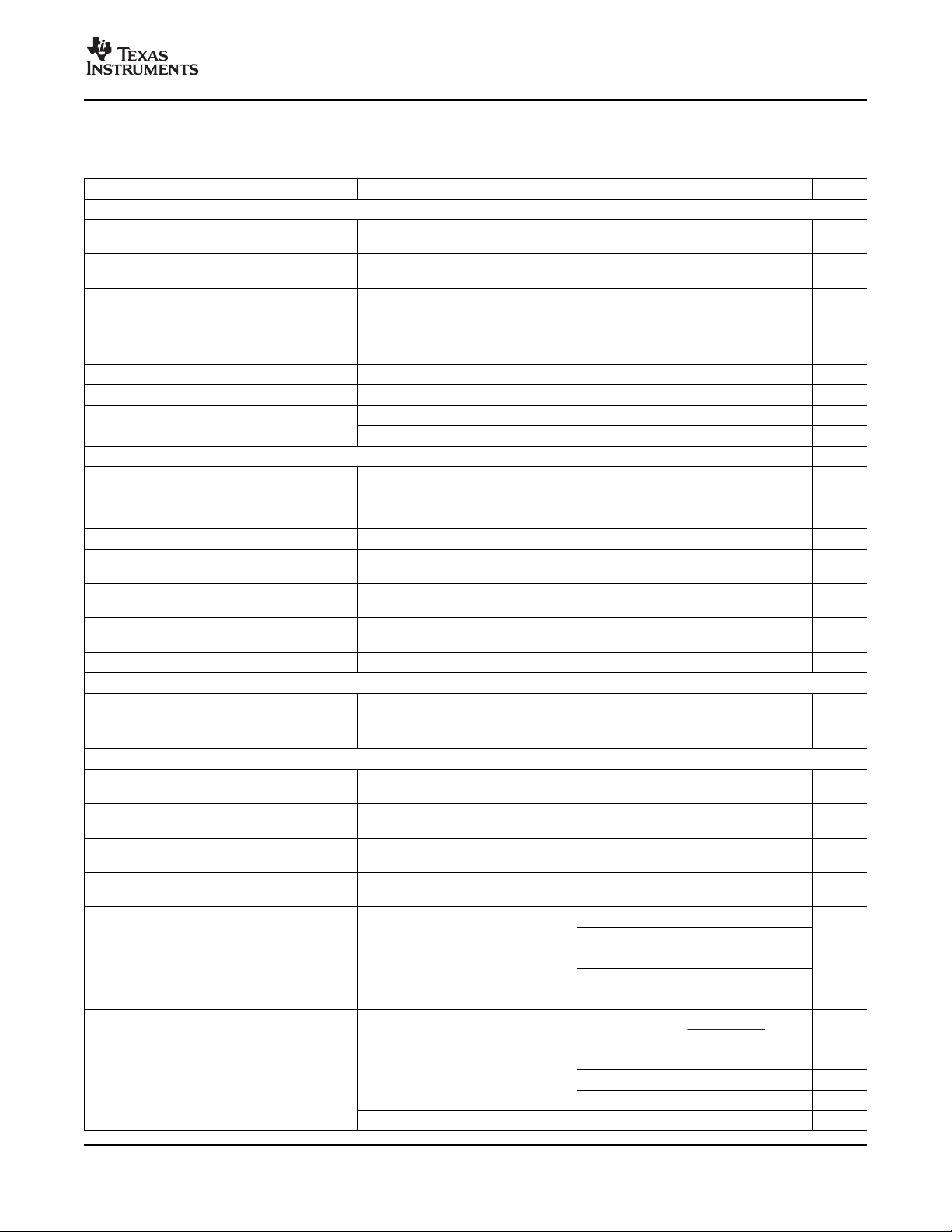
NOTES:
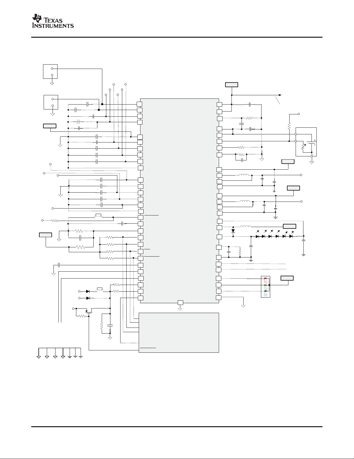
1) RESISTORVALUESINOHMS
2) THEFOLLOWINGPARAMETERS AREPROGRAMMED :
- R
TMR
=
49.9K: 6 HOURCHARGESAFETY TIMER ,
30 MINPRE-CHARGESAFETY TIMER
- R
SET
= 1K: 1A CHARGECURRENT (NOSCALING , INPUTLIMIT=2.5A),
100 mATERMINATION ANDPRE - CHARGECURRENTS
- R
FB
3
=
10 OHMS: 25
mA WHITELEDCURRENT
- C
TRSTPWON
=
100
nF : 100mSECRESETPULSEWIDTH
- R
DPPM
=
37.4K:
V
(DPPM)
=
4.3V
3) THECAPACITORVALUESSHOWNINTHE APPLICATIONDIAGRAM
MAY BELARGERTHANTHEMINIMUMREQUIREDVALUESINDICATED
INTHEPINDESCRIPITONTABLE
4) THEVALUESSHOWNINTHE APPLICATIONDIAGRAMMATCHTHE
COMPONENTVALUESUSEDINTHEHPA 129 EVM, SEEDESIGNNOTES
SECTIONFORCOMPONENTSELECTIONDETAILS
5) AFTERGPIOS ARESETTOHITHEHOSTNEEDSTOTURNONM1IN
LESSTHAN 1 SEC (WITHR8 =100K ANDC29=4.7uF ) TOKEEP THE
SYSTEMRUNNINGUNDERBATTERY POWERONLY
VOUT
VOUT
VOUT
VOUT
EXTERNAL
PERIPHERALS
VOUT
WHITELEDS
VOUT
VOUT
57
PWRGND
A 1
R
SET
R
TMR
R
DPPM
C
TRSTPWON
C 1
C 2
C 3
C 4
C 5
C 6
C 7
C 8
C 9
C 10
C 11
C 12
C 13
C 14
C 15
C 16
C 17
C 18
C 19
C 20
C 21
C 22
C 23
C 24
C 25
C 26
R 1
R 2
R 3
R 4
R 5
R 6
R
FB3
LSM 1
LSM 2
LSM 3
C 27
D 1
RGBLED
V SM2
100 K
R 7
V
LDO_PM
SYSTEM_ON
BAT
V SM2
A 1
M1
100KΩ
R 9 1 K
R 10
1 K
RESETSWITCH
TURNONSWITCH
V SM2
P 3
1 uF
C 28
R 8
C 29
100 K
4 .7 uF
R
12
10KΩ
V
SIM
R
11
TPS65810
TPS65811
SLVS658B – MARCH 2006 – REVISED FEBRUARY 2007
APPLICATION DIAGRAM
Copyright © 2006 – 2007, Texas Instruments Incorporated Submit Documentation Feedback 21
Figure 3. TPS65810 Application Diagram, Recommended External Components
Product Folder Link(s): TPS65810 TPS65811

www.ti.com
I
BAT
V
USB
V
OUT
V
BAT
USB=5V,
BAT =3.3V
I
BAT
V
AC
V
OUT
V
BAT
AC=5V,
BAT =3.3V
TPS65810
TPS65811
SLVS658B – MARCH 2006 – REVISED FEBRUARY 2007
TYPICAL CHARACTERISTICS – POWER PATH MANAGEMENT
Measured with Application Circuit shown in Figure 3 (unless otherwise noted).
SWITCHING FROM AC TO BATTERY SWITCHING FROM USB TO BATTERY
ON AC REMOVAL ON USB REMOVAL
Figure 4. Figure 5.
22 Submit Documentation Feedback Copyright © 2006 – 2007, Texas Instruments Incorporated
Product Folder Link(s): TPS65810 TPS65811
www.ti.com
0
0.05
0.1
0.15
0.2
0.25
0 20 40 60 80 100 120 140
LineRegulation-%
VIN_LDO02=3.8Vto4.7V,
Load=10mA,
C (LDO02)=1 FOm
T -JunctionTemperature-°C
J
VIN_LDO02=3.65V,
Load=10mA to150mA,
C (LDO02)=1 FOm
-0.850
-0.800
-0.750
-0.700
-0.650
-0.600
-0.550
-0.500
0 20 40 60 80 100 120 140
T -JunctionTemperature-°C
J
LoadRegulation-%
VIN_LDO02=3.3V,
Load=150mA,C =1 F
O(LDO02)
m
70
80
90
100
110
120
130
140
0 20 40 60 80 100 120 140
DropoutVoltage-mV
T -JunctionTemperature-°C
J
VIN_LDO02=3.65V,Load=10mA,
V =3.3V,
O(LDO 0)
V =1.225V
O(LDO 1,2)
1
1.5
2
2.5
3
3.5
0 20 40 60 80 100 120 140
V
-OutputVoltage-V
O
LDO0
LDO1
LDO2
T -JunctionTemperature-°C
J
SLVS658B – MARCH 2006 – REVISED FEBRUARY 2007
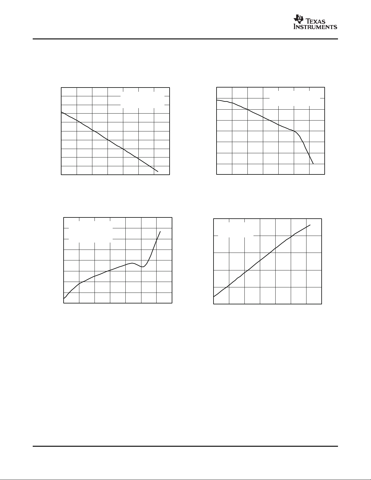
TYPICAL CHARACTERISTICS – LINEAR REGULATORS 0, 1, 2
Measured with application circuit shown in Figure 3 (unless otherwise noted).
TPS65810
TPS65811
LOAD REGULATION LINE REGULATION
vs vs
JUNCTION TEMPERATURE JUNCTION TEMPERATURE
Figure 6. Figure 7.
OUTPUT VOLTAGE DROPOUT VOLTAGE
vs vs
JUNCTION TEMPERATURE JUNCTION TEMPERATURE
Copyright © 2006 – 2007, Texas Instruments Incorporated Submit Documentation Feedback 23
Figure 8. Figure 9.
Product Folder Link(s): TPS65810 TPS65811
www.ti.com
VIN_LDO35=3V,
Load=10mA to150mA,
C =1 F
O(LDO 35)
m
-1
-0.95
-0.90
-0.85
-0.80
-0.75
-0.70
-0.65
-0.6
-0.55
-0.5
0 20 40 60 80 100 120 140
LoadRegulation-%
T -JunctionTemperature-°C
J
-0.018
-0.017
-0.016
-0.015
-0.014
-0.013
-0.012
-0.011
-0.010
0 20 40 60 80 100 120 140
LineRegulation-%
VIN_LDO35=3.3Vto4.7V,
Load=100mA,
C (LDO35)=1 FOm
T -JunctionTemperature-°C
J
1.2285
1.229
1.2295
1.23
1.2305
1.231
1.2315
1.232
1.2325
0
20
40 60 80
100 120 140
VIN_LDO35=4.7V,
Load=10mA,
V (LDO35)=1.228V,
C (LDO35)=1 F
O
O
m
T -JunctionTemperature-°C
J
V -OutputVoltage-V
O
90
100
110
120
130
140
0 20 40 60 80 100 120 140
Dropout-mV
VIN_LDO35=3.3V,
Load=150mA,
C (LDO35)=1 FOm
T -JunctionTemperature-°C
J
TPS65810
TPS65811
SLVS658B – MARCH 2006 – REVISED FEBRUARY 2007
TYPICAL CHARACTERISTICS – LINEAR REGULATORS 3, 4, 5
Measured with application circuit shown in Figure 3 (unless otherwise noted).
LOAD REGULATION LINE REGULATION
vs vs
JUNCTION TEMPERATURE JUNCTION TEMPERATURE
Figure 10. Figure 11.
OUTPUT VOLTAGE DROPOUT VOLTAGE
vs vs
JUNCTION TEMPERATURE JUNCTION TEMPERATURE
24 Submit Documentation Feedback Copyright © 2006 – 2007, Texas Instruments Incorporated
Figure 12. Figure 13.
Product Folder Link(s): TPS65810 TPS65811
www.ti.com
0
10
20
30
40
50
60
70
80
90
100
0 0.1 0.2 0.3 0.4 0.5 0.6
I -OutputCurrent- A
O
Efficiency-%
VIN_SM1=4V,
V (SM1)=1.24V,
L =3.3 H,
C (SM1)=10 F
O
O
m
m
76
78
80
82
84
86
88
90
92
0 0.1 0.2 0.3
0.4
0.5 0.6 0.7
I -OutputCurrent- A
O
Efficiency-%
VIN_SM2=4.6V,
VO(SM2)=1.8V,
L =3.3 H.
C (SM2)=10 FOm
m
AC=5V,
VIN_SM2=4.6V,
V (SM2=1.8V
O
I (SM2)
L =3.3mF,
C (SM2)=10 F
O
O
m
AC=5V,
VIN_SM2=4.6V,
V (SM2=1.8V
O
I (SM2)
L =3.3mF,
C (SM2)=10 F
O
O
m
SLVS658B – MARCH 2006 – REVISED FEBRUARY 2007
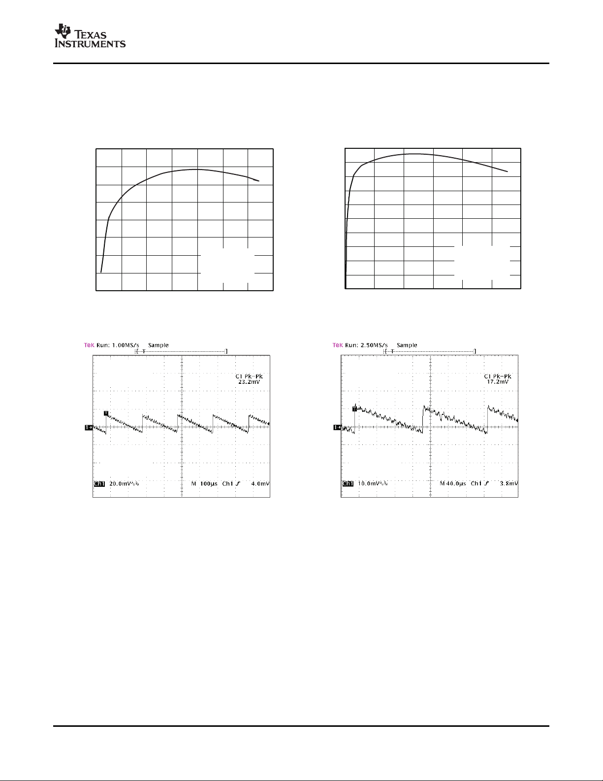
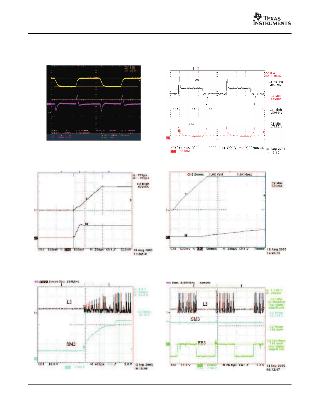
TYPICAL CHARACTERISTICS – SM1 AND SM2 BUCK CONVERTERS
Measured with application circuit shown in Figure 3 (unless otherwise noted).
EFFICIENCY IN AUTOMATIC vs
PWM/PFM MODE OUTPUT CURRENT
Figure 14. Figure 15.
TPS65810
TPS65811
PWM MODE
EFFICIENCY
PFM OPERATION PFM LOW RIPPLE OPERATION
Copyright © 2006 – 2007, Texas Instruments Incorporated Submit Documentation Feedback 25
Figure 16. Figure 17.
Product Folder Link(s): TPS65810 TPS65811
www.ti.com
VIN_SM2
VO(SM2)
AC=5V,VIN_SM2=3V(DC)+1V(AC),
V (SM2)=1.8V,I (SM2)=100mA,
L =3.3 F,C (SM1)=10 F,
CH1=VIN_SM2,CH2=V (SM2)
O O
O
O
m m
VO_SM2
I (SM2)
O
AC=5V,
VIN_SM2=4V,
V (SM2)=1.8V,
I (SM2)=0mA to600mA,
L =3.3 F,C (SM1)=10 F,
CH1=VO_SM2,
CH3=I (SM2)
O
O
O
m m
O
SM2Voltage
SM2Current
AC=5V,
VIN_SM2/SM2=4V,
V (SM2)=1.8V,
I (SM2)=600mA,
L =3.3 F,
C (SM1)=10 F
O
O
O
m
m
SM1Voltage
SM1Current
AC=5V,
VIN_SM2/SM2=4V,
V (SM2)=1.8V,
I (SM2)=600mA,
L =3.3 F,
C (SM1)=10 F
O
O
O
m
m
BAT =4V,
DC=0%
L3=4.7 F,
C (SM3)=10 F,
CH1=L3,
CH4=SM3
m
m
O
BAT =4V,DC=0%
L3=4.7 F,C (SM3)=10 F,
CH1=L3,CH4=SM3
m m
O
TPS65810
TPS65811
SLVS658B – MARCH 2006 – REVISED FEBRUARY 2007
Measured with application circuit shown in Figure 3 (unless otherwise noted)
LINE TRANSIENT LOAD TRANSIENT
Figure 18. Figure 19.
TRANSIENT - SM1 STARTUP TRANSIENT - SM2 STARTUP
TYPICAL CHARACTERISTICS – DRIVERS
26 Submit Documentation Feedback Copyright © 2006 – 2007, Texas Instruments Incorporated
Figure 20. Figure 21.
SM3 WHITE LED DRIVER vs
SOFT START PWM DUTY CYCLE
Figure 22. Figure 23.
Product Folder Link(s): TPS65810 TPS65811
SM3 LED CURRENT

www.ti.com
TPS65810
TPS65811
SLVS658B – MARCH 2006 – REVISED FEBRUARY 2007
SERIAL INTERFACE
Overview
The TPS65810 is compatible with a host-controlled environment, with internal parameters and status information
accessible via an I2C interface. An I2C communication port provides a simple way for an I2C compatible host to
access system status information and reset fault modes, functioning as a SLAVE port enabling I2C compatible
hosts to WRITE to or to READ from internal registers. The TPS65810 I2C port is a 2-wire bidirectional interface
using SCL (clock) and SDA (data) pins; the SDA pin is open drain and requires an external pullup. The I2C is
designed to operate at SCL frequencies up to 400 kHz. The standard 8 bit command is supported, the CMD part
of the sequence is the 8 bit register address to READ from or to WRITE to.
Register Default Values
The internal TPS65810 registers are loaded during the initial power-up from an internal, non-volatile memory
bank. The power-up default values are described in the sections detailing the registers functionality.
The register contents remain intact as long as OUT pin voltage remains above the internal UVLO threshold,
V
. All register bits are reset to the internal power up default when the OUT pin voltage falls below the V
UVLO
threshold or if the HOT_RESET pin is set to LO.
I2C Address
The I2C specification contains several global addresses, which the slaves on the bus are required to respond to.
The TPS65810 only responds (ACK) to addresses: 0x90 and 0x91 and does not respond (NACK) to any other
address.
UVLO
Table 1. TPS65810 I2C Read/Write Address
BYTE BIT
MSB 6 5 4 3 2 1 LSB
TPS65810 I2C WRITE ADDRESS 1 0 0 1 0 0 0 0
TPS65810 I2C READ ADDRESS 1 0 0 1 0 0 0 1
I/O DATA BUS B7 B6 B5 B4 B3 B2 B1 B0
Incremental Read
The TPS65810 does not support incremental read operations. Each register must be accessed in a single read
operation.
I2C Bus Release
The TPS65810 I2C engine does not create START or STOP states on the I2C bus during normal operation.
Sleep Mode Operation
When the sleep mode is set SDAT is held LO by the TPS65810. The overall system operation is not affected, as
in sleep mode all TPS65810 integrated supplies are disabled and no power is available for any external devices
connected to the TPS65810 SDAT pin. When sleep mode ends the SDAT pin is released before the TPS65810
integrated regulated supplies are enabled. See section on System Sequencing and TPS65810 Operating Modes
for additional details on sleep mode operation.
I2C Communication Protocol
The following conventions are used when describing the communication protocol:
Table 2. I2C Naming Conventions Used
CONDITION CODE
START sent from host S
STOP sent from host P
TPS65810 I2C slave address sent from host, bus direction set from host to TPS65810 (WRITE) hA0
Copyright © 2006 – 2007, Texas Instruments Incorporated Submit Documentation Feedback 27
Product Folder Link(s): TPS65810 TPS65811
www.ti.com
STOP
CONDITION
(P)
START
CONDITION
(S)
BIT 7
MSB
BIT 6
BIT0
LSB
ACKNOWLEDGE
(hAorbqA)
STOP
CONDITION
(P)
SCL
SDA
STOP
CONDITION
(P)
START
CONDITION
(S)
BIT 7
MSB
BIT 6
BIT 0
LSB
NOT
ACKNOWLEDGE
(hNorbqN)
STOP
CONDITION
(P)
SCL
SDA
STOP
CONDITION
(P)
START
CONDITION
(S)
BIT 7
MSB
BIT 6
SCL
SDA
DATA LINE
STABLE
DATA
CHANGE
ALLOWED
BIT 5-1
TPS65810
TPS65811
SLVS658B – MARCH 2006 – REVISED FEBRUARY 2007
Table 2. I2C Naming Conventions Used (continued)
CONDITION CODE
TPS65810 register address sent from TPS65810, bus direction is from TPS65810 to host (READ) hA1
Non-valid I2C slave address sent from host hA_N
Valid TPS65810 register address sent from host HCMD
Non-valid TPS65810 register address sent from host HCMD_N
I/O data byte (8 bits) sent from host to TPS65810 hDATA
I/O data byte (8 bits) sent from TPS65810 to host bqDATA
Acknowledge (ACK) from host hA
Not acknowledge (NACK) from host hN
Acknowledge (ACK) from TPS65810 bqA
Not acknowledge (NACK) from TPS65810 bqN
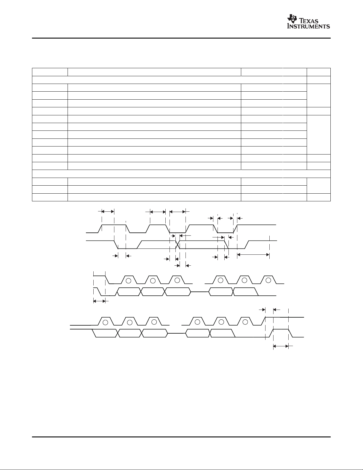
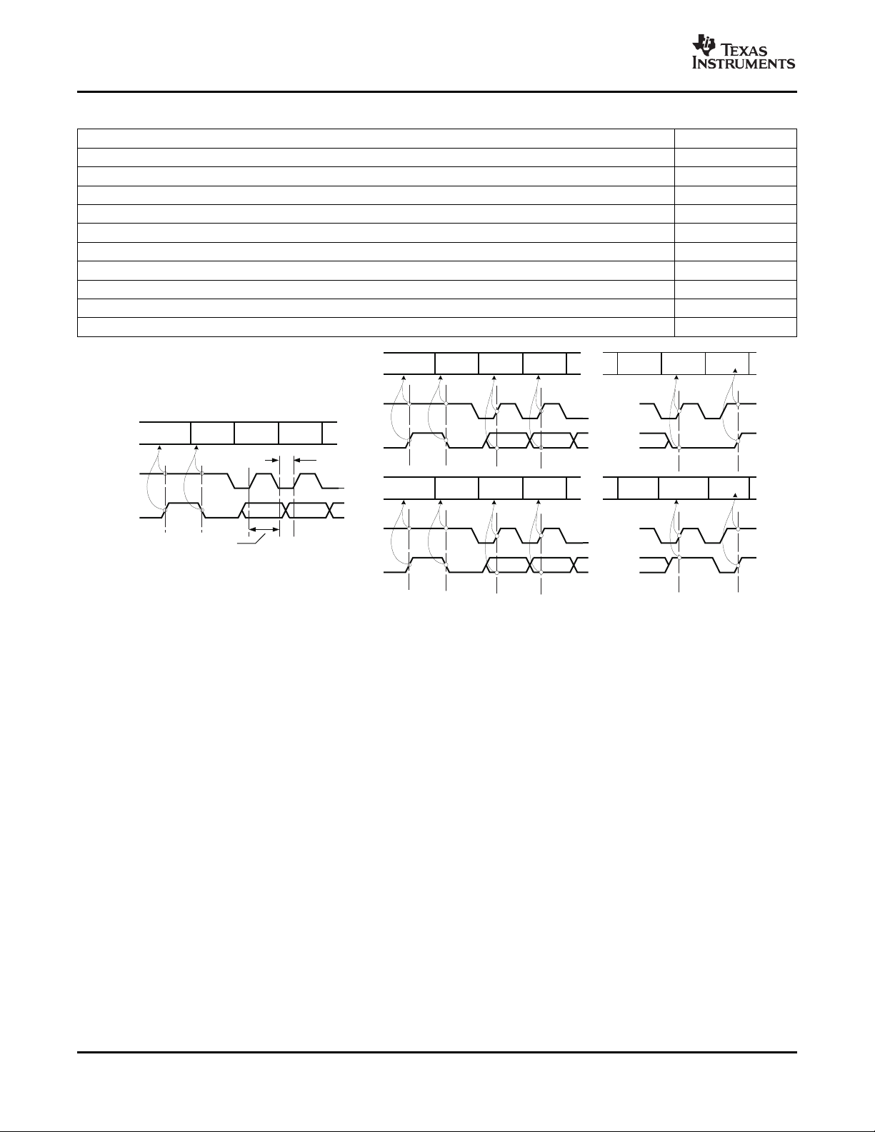
Figure 24. I2C operation waveforms
For normal data transfers, SDA is allowed to change only when SCL is low, and one clock pulse is used per bit
of data. The SDA line must remain stable whenever the SCL line is high, as SDA changes when SCL is high are
reserved for indicating the start and stop conditions. Each data transfer is initiated with a start condition and
terminated with a stop condition.
When addressed, the TPS65810 device generates an acknowledge bit after the reception of each byte by pulling
the SDA line Low. The master device (microprocessor) must generate an extra clock pulse that is associated
with the acknowledge bit. After the acknowledge/not acknowledge bit the TPS65810 leaves the data line high,
enabling a STOP condition generation.
I2C Read and Write Operations
The TPS65810 supports the standard I2C one byte Write. The basic I2C read protocol has the following steps:
• Host sends a start and sets TPS65810 I2C slave address in write mode
• TPS65810 ACK ’ s that this is a valid I2C address and that the bus is configured for write
• Host sends TPS65810 register address
• TPS65810 ACK ’ s that this is a valid register and stores the register address to be read
• Host sends a repeated start and TPS65810 I2C slave address, reconfiguring the bus for read
• TPS65810 ACK ’ s that this is a valid address and that bus is reconfigured
• Bus is in read mode, TPS65810 starts sending data from selected register
The I2C write protocol is similar to the read, without the need for a repeated start and bus being set in write
mode. In a WRITE, it is not necessary to end each 1-byte WRITE command with a STOP; a START has the
same effect (repeated start).
28 Submit Documentation Feedback Copyright © 2006 – 2007, Texas Instruments Incorporated
Product Folder Link(s): TPS65810 TPS65811
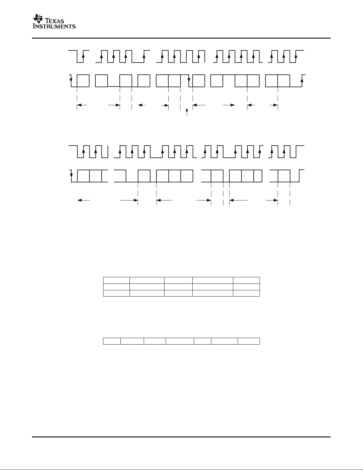
www.ti.com
SCLK ... ......
SDAT
Slave Address
hA0
Slave Address
hA1
Register
Address
hCMD
....
A6 R0R7R/WA0
0
0
0 0
Start
...
..
D0D7R/WA0A6
1
Slave
Drives
theData
bqDATA
MasterDrives
ACKandStop
RepeatedStart, canbereplacedbya
STOP andSTART
..
SCLK
... ......
SDAT
Slave Address
hA0
HostSends
Data
hDATA
Register
Address
hCMD
.........
A6 R6 R5 R0 D7 D6 D5 D0R7R/WA0A4A5
0 0 0 0
PStart
bqA bqA bqA hA PS
bqA bqA bqA
ACK
ACK
ACK
ACK
ACK
ACK
ACK
TPS65810
TPS65811
SLVS658B – MARCH 2006 – REVISED FEBRUARY 2007
The host can complete a READ or a WRITE sequence with either a STOP or a START.
Valid Write Sequences
The TPS65810 always ACKs its own address. If the CMD points to an allowable READ or WRITE address, bq
writes the address into its RAM address register and sends an ACK. If the CMD points to a non-allowed address,
bq does NOT write the address into its RAM address register and sends a NACK.
One-Byte Write
The data is written to the addressed register when the bq ACK ending the one byte write sequence is received.
The host can cancel a WRITE by sending a STOP or START before the trailing edge of the bq ACK clock pulse.
Figure 25. I2C read and write operations
S hA0 bqA
S hA0 bqA hCMD bqA
S hA0 bqA hCMD_N bqN
S hA0 bqA hCMD bqA hDATA bqA
Copyright © 2006 – 2007, Texas Instruments Incorporated Submit Documentation Feedback 29
Product Folder Link(s): TPS65810 TPS65811

www.ti.com
TPS65810
TPS65811
SLVS658B – MARCH 2006 – REVISED FEBRUARY 2007
Valid Read Sequences
The TPS65810 always ACKs its own address.
S hA1 bqA
Upon receiving hA1, TPS65810 starts at wherever the RAM address register is pointing. The START and the
STOP both act as priority interrupts. If the host has been interrupted and is not sure where it left off it can send a
STOP and reset the TPS65810 state machine to the WAIT state; once in WAIT state, the TPS65810 ignores all
activity on the SCL and SDA lines until it receives a START. A repeated START and START in the I2C
specification are both treated as a START.
S hA0 bqA hCMD bqA P
S hA0 bqA hCMD bqA S hA1 bqA bqDATA hN P
S hA1 bqA bqDATA hN P
Non-Valid Sequences
Incremental read sequences
S hA1 bqA bqDATA hA bqDATA hA bqDATA hA bqDATA hA ... bqDATA hA P
START and non-hA0 or non-hA1 Address
A START followed by an address which is not bqA0 or bqA1 is NACKED.
S hA_N bqN
Attempt to Specify Non-Allowed READ Address
If the CMD points to a non-allowed READ address (reserved registers), bq sends a NACK back to the host, and
it does not load the address in the RAM address register. Note that TPS65810 NACKS whether a stop is sent or
not.
S hA0 bqA hCMD_N bqN P
S hA0 bqA hCMD_N bqN
Attempt to Specify Non-Allowed WRITE Address
If the host attempts to WRITE to a READ-ONLY or non-accessible address TPS65810 ACKS the CMD
containing the allowed READ address, loads the address into the address register and NACKS after the host
sends the next data byte. After issuing the NACK TPS65810 returns to WAIT state. A subsequent hA1 READ
could read this address.
S hA0 bqA hCMD bqA hDATA bN
30 Submit Documentation Feedback Copyright © 2006 – 2007, Texas Instruments Incorporated
Product Folder Link(s): TPS65810 TPS65811

www.ti.com
SLVS658B – MARCH 2006 – REVISED FEBRUARY 2007
TPS65810 INTERNAL REGISTER MAP
hex NAME DESCRIPTION ADDITIONAL
0 RESERVED_01 RESERVED FACTORY ONLY
1 RESERVED_02 RESERVED FACTORY ONLY
2 PGOOD Output voltage status for linear regulators and dc/dc buck converters
3 INTMASK1 Interrupt request masking settings
4 INTMASK2 Interrupt request masking settings
5 INT_ACK1 Masked interrupt request register, latched
6 INT_ACK2 Masked interrupt request register, latched
7 PGOODFAULT_MASK System Reset masking settings
8 SOFT_RESET Generates a software reset
9 CHG_CONFIG Battery charger configuration
A CHG_STAT Battery charger status
B EN_LDO Linear regulator ON/OFF control
C LDO12 LDO1 and LDO2 output voltage setting
D LDO3 LDO3 output voltage settings
E LDO4 LDO4 output voltage settings
F LDO5 LDO5 output voltage settings
10 SM1_SET1 SM1 Buck converter ON/OFF control and output voltage setting, normal mode
11 SM1_SET2 SM1 Buck converter configuration
12 SM1_STANDBY SM1 Buck converter standby mode ON/OFF and standby output voltage setting
13 SM2_SET1 SM2 Buck converter ON/OFF control and output voltage setting, normal mode
14 SM2_SET2 SM2 Buck converter configuration
15 SM2_STANDBY SM2 Buck converter standby mode ON/OFF and standby output voltage setting
16 SM3_SET SM3 White LED driver ON/OFF control and settings
17 RGB_FLASH Overall RGB driver timing settings
18 RGB_RED RGB driver: RED duty cycle and output current setting
19 RGB_GREEN RGB driver: GREEN duty cycle and output current setting
1A RGB_BLUE RGB driver: BLUE duty cycle and output current setting
1B GPIO12 GPIO1 and GPIO2 configuration
1C GPIO3 GPIO2 and GPIO3 configuration, battery charge voltage selection
1D PWM PWM output configuration
1E ADC_SET ADC On/OFF control, ADC configuration
1F ADC reading_hi ADC data output
20 ADC reading_lo ADC data output
21 DHILIM1 ADC Maximum threshold setting
22 DHILIM2 ADC Maximum threshold setting
23 DLOLIM1 ADC Minimum threshold setting
24 DLOLIM2 ADC Minimum threshold setting
25 ADC_DELAY ADC configuration: conversion delay
26 ADC_WAIT ADC configuration: wait and repeat operation
27 LED_PWM LED_PWM configuration
2E RESERVED_03 RESERVED FACTORY ONLY
TPS65810
TPS65811
DETAILS
Copyright © 2006 – 2007, Texas Instruments Incorporated Submit Documentation Feedback 31
Product Folder Link(s): TPS65810 TPS65811

www.ti.com
INTERRUPT
CONTROLLER
INT
SDAT
SCLK
STATEMACHINE
ANDRESET
CONTROLLER
HOT_RST
RESPWRON
TRSTPWON
SYS_IN
HOST INTERFACE
ANDSEQUENCING
I2CENGINE
OUT
0. 1uF
A 1
2K
10 0K
2K
HOST
TPS 65810
10 0K
A1
A1
R5
R3
R 2
R 4
C
TRSTPWON
210 K
R 6
R 1
100 K
C 16
100 nF
10 0K
V SM2
R7
TPS65810
TPS65811
SLVS658B – MARCH 2006 – REVISED FEBRUARY 2007
FUNCTIONALITY REFERENCE GUIDE – HOST INTERFACE AND SYSTEM SEQUENCING
INTERRUPT CONTROLLER, OPEN-DRAIN OUTPUT (INT)
System Parameters Monitored by Interrupt Controller Power up
Supply Output System
Power Good Fault Status ADC status
Detection
LDO1, LDO2, External resistive
LDO3, LDO4, load connected to
(1)
SM1, ADC conversion end
SM2, ADC
SM3, Input out of range
Modification
Thermal Fault or ↔ Done AC detected: yes ↔ no
GPIO 1,2 DPPM:on ↔ off USB detected: yes ↔ no
configured as Charge Suspend: on ↔ Input OVP: yes ↔ no
external interrupt off System Power: AC ↔
LDO5 ANLG1
request Thermal Foldback: on USB
Can be masked Individually
via I2C. Blanked during Can be masked Individually via I2C
initial power up
Charger Status Input and Output
Transition Power Transition
Charge: Pre ↔ Fast
↔ off
Can be masked as a group via a single I2C mask
register bit
(1) For all supplies (except) for SM3 an output fault is detected if the output voltage is below 90% of the programmed regulation voltage. In
the SM3 converter an output fault indicates that the output OVP threshold was reached.
EVENTS TRIGGERING TPS65810 OPERATING MODE CHANGES
EVENT POWER GOOD FAULT THERMAL HARDWARE SOFTWARE
DETECTION
(1)
FAULT RESET RESET
How transition is Integrated regulator output Internal IC junction Using HOT_RST control I2C register control bit
triggered voltage below target value: temperature pin
SM1, SM2, SM3, LDO1,
LDO2,LDO3, LDO4, LDO5
Operating mode Sets Sleep mode or starts a Sets Sleep mode when Generates external host Generates external host
change new power-up cycle when thermal fault is detected reset pulse at pin reset pulse at pin
power good fault is detected RESPWON when RESPWON when I2C
(see state machine diagram). HOT_RST=LO. control bit is set.
Power good fault detection Input and Battery power Pulse duration set by Pulse duration set by
comparators are blanked during cycling required to exit external capacitor. external capacitor.
initial power-up. sleep
Controls Can be masked Individually via Fixed Internal Threshold External Input Set via I2C
I2C.
(1) For all supplies (except) for SM3 an output fault is detected if the output voltage is below 90% of the programmed regulation voltage. In
the SM3 converter an output fault indicates that the output OVP threshold was reached.
default
All interrupt
controller
inputs set to
non-masked
Figure 26. Required External Components, Recommended Values, External Connections
32 Submit Documentation Feedback Copyright © 2006 – 2007, Texas Instruments Incorporated
Product Folder Link(s): TPS65810 TPS65811
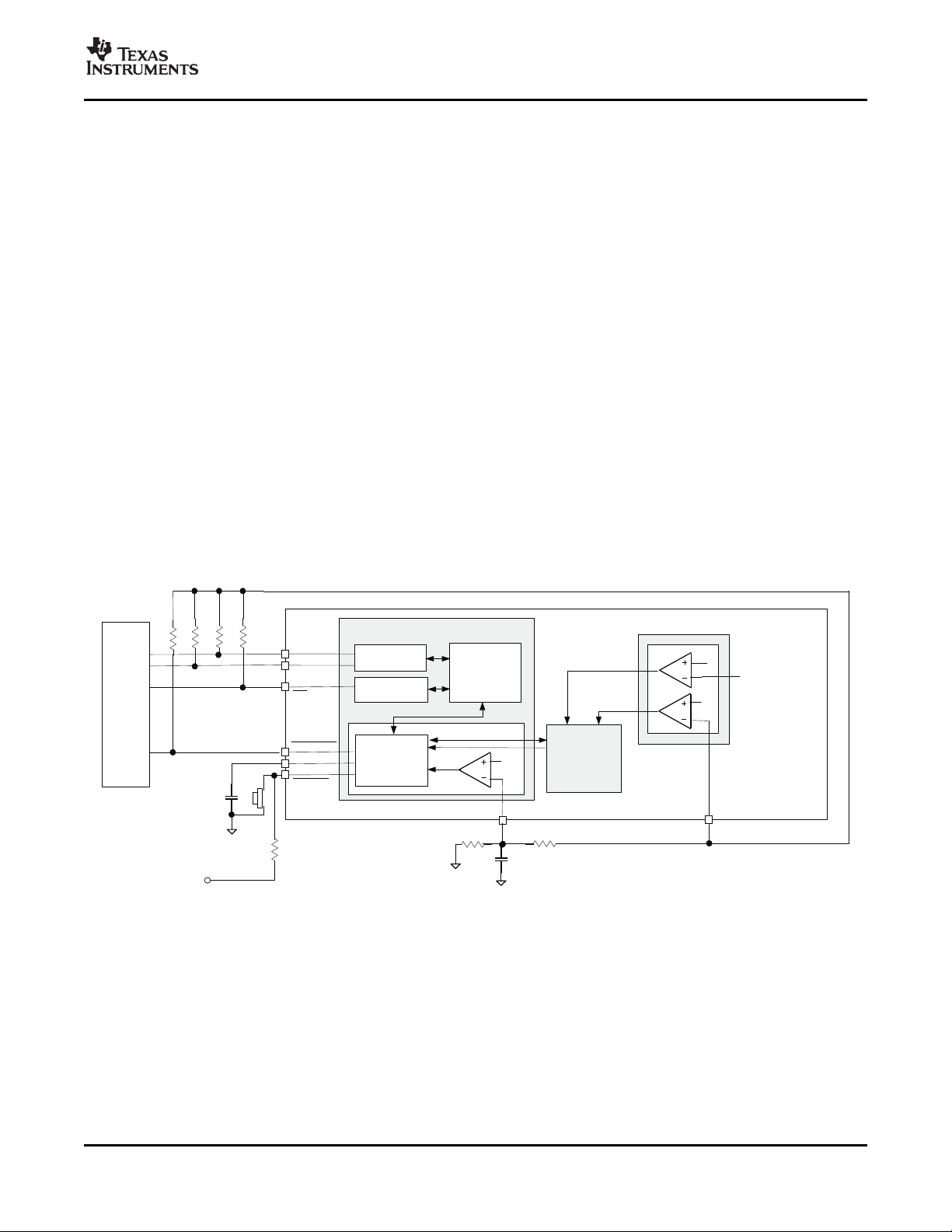
www.ti.com
INT
SDAT
SCLK
SEQUENCING
ANDOPERATING
MODESETTING
HOT _ RST
RESPWRON
TRSTPWON
SYS _IN
HOSTINTERFACE ANDSEQUENCING
I2 CENGINE I2 CREGISTERS
ANDNON -
VOLATILE
MEMORY
CONTROL
LOGIC
2 .5V
1 V
AC /USB /BAT
(HIGHERVOLTAGE
)
VSYS
OUT
A 1
HOST
TPS65810
R 1
R 6
A 1
C 16
R 5
R 3
R 2
R 4
C
TRSTPWON
2. 5V
1 0 0 K
V SM 2
R 7
INTERRUPT
CONTROLLER
TPS65810
TPS65811
SLVS658B – MARCH 2006 – REVISED FEBRUARY 2007
INTERRUPT CONTROLLER AND SYSTEM SEQUENCING
Overview
The TPS65810 has two dedicated internal controllers that execute the host interface and system sequencing
tasks: a sequencing controller and an interrupt controller.
The sequencing controller monitors internal and system parameters and defines the sequencing of the internal
power supplies during power up and power down / power fault events, and executes specific internal power
supply reset operations under external hardware control or host software commands.
The following parameters are monitored by the sequencing controller:
• System power bus voltage (at SYS_IN pin), input supply voltage, battery pack voltage
• TPS65810 thermal fault status
• Integrated supply status
The interrupt controller monitors multiple system status parameters and signals to the host when one of the
monitored parameters toggled, as a result of a system status change. The interrupt controller inputs include all
the parameters monitored by the sequencing controller plus:
• Charger status
• Battery pack status
• ADC status
Internal I2C registers enable masking of all the monitored parameters. Using those registers, the host can select
which parameters trigger an interrupt or a power-good fault. Power-good faults trigger a change in the TPS65810
operating mode, as detailed in the next sections.
A simplified block diagram for the TPS65810 sections that interface to the external host is shown in Figure 27 .
Figure 27. Simplified Block Diagram
Copyright © 2006 – 2007, Texas Instruments Incorporated Submit Documentation Feedback 33
Product Folder Link(s): TPS65810 TPS65811

www.ti.com
SLEEP STATE
ONLY RTC_ LDOISON
POWERPATH ACTIVE
RESPWRON = 0
REGISTERCONTENTSNOT RESET
INTERRUPT CLEARED
OFF
PROCESSOR
STANDBY STATE
RESPWRON = HI
PGFORSM1&SM2
ismasked
ENABLESTATE
SEQUENCESTATE
START INTEGRATED
SUPPLY START - UP SEQUENCE
RESPWRON
= LO
POWERGOOD
CHECKSTATE
RESPWRON=HI
ENABLEPOWERGOODCOMPARATORS
INT PINMODESET BY INTERRUPT
CONTROLLER
NORMAL MODE
RESPWRON=HI
ANY
STATE
RESETSTATE
RESPWRON=LO
START SYSTEMRESET PULSE TIMER
WHENHOT_RESET=HI
RESET
TIMEREXPIRES
V(SYS_IN) > AND
V(OUT) > V
V
(LOW_SYS)
V(AC) > V
UVLO
OR
V(USB) > V
UVLO
OR
V(BAT) > V
UVLO
NOPGOOD
FAULT
STANDBY
ON
STANDBY
OFF
PGOOD
FAULT
PGOOD
FAULT
V(OUT) < V
UVLO
RESPWRON=LO
V(SYS_IN) <
OR
POWER
CYCLE
AND
SLEEP NOT SET BY
THERMAL FAULT
THERMAL
FAULT
V(HOT_RESET)= LO
OR
I2CSOFT_RESET
REGISTERBIT
SOFT_RST = HI
V(HOT_RESET)= HI OR
I2CSOFT_RESET
REGISTERBIT
SOFT_RESET = LO
(SELFCLEARED)
V(HOT_RESET)= LO
OR
I2CSOFT_RESET
REGISTERBIT
SOFT_RST= HI
PGOODFAULT : A NON - MASKEDBIT OF THE
POWER _GOODI2CREGISTER TOGGLES
FROMLO TOHI
STANDBY ON : SM1 ANDSM 2 SET INSTANDBY
MODEBY GPIOORI 2CCOMMAND
STANDBY OFF : SM1 ANDSM 2 EXIT STANDBY
MODEBY GPIOOR
I2CCOMMAND
RESETTIMER : VALUESET BY CAPACITOR
CONNECTED TO TRSTPWONPIN
I2CSOFT_RESETBIT LOCATEDIN
SOFT_RESET REGISTER , BIT B0
POWERUP
OR
I2CSOFT_ RESET
REGISTER
BIT SLEEP _MODE = HI
(SELF-CLEARED )
RESPWRON=LO
UVLO
V
(LOW_SYS)
LOADPOWERUP DEFAULTSIN
I2CREGISTERS
CONNECT AC, USBORBAT PIN TO
OUT PIN
DISABLEPOWERGOODFAULT
DETECTION
INT PIN = HIGHIMPEDANCE
POR_FLAG = HI
POWERUP DEFAULTSLOADED
IN ALL I2CREGISTERS
(ExceptINT_ACKn)
POWERDOWNRAILS,
WAIT 5msec
TPS65810
TPS65811
SLVS658B – MARCH 2006 – REVISED FEBRUARY 2007
SYSTEM SEQUENCING AND TPS65810 OPERATING MODES
The TPS65810 has a state machine that controls the device power up and power down sequencing. The main
operating modes are shown in the state diagram below:
POWER UP – If the AC, USB and BAT pin voltages are below the internal UVLO threshold V
IC blocks are disabled and the TPS65810 is not operational, with all functions OFF. When an external power
source or battery with voltage greater than the V
internal TPS65810 references are powered up, biasing internal circuits. When all the main internal supply rails
are active the TPS65810 I2C registers are set to the power-up default values, shown below:
34 Submit Documentation Feedback Copyright © 2006 – 2007, Texas Instruments Incorporated
Figure 28. TPS65810 State Diagram
Product Folder Link(s): TPS65810 TPS65811
UVLO
voltage threshold is applied to AC/USB or BAT pins the
UVLO
(2.5 V typ) all

www.ti.com
V(OUT) + V
(LOW_SYS)
ǒ
1 )
R6
R1
Ǔ
:
where R6 and R1 are external resistors, V
(LOW_SYS)
+ 1 V typical
TPS65810
TPS65811
SLVS658B – MARCH 2006 – REVISED FEBRUARY 2007
Table 3. Integrated Supply and Drivers I2C Registers Power-Up Defaults
SUPPLY POWER-UP DEFAULT OTHER BLOCKS POWER-UP DEFAULT
LDO0 OFF, 3.3 V POWER PATH INPUT TO SYSTEM
LDO1 1.25V, OFF PWM OFF
LDO2 3.3 V, OFF PWM_LED OFF
LDO3 1.505 V, OFF GPIO1 INPUT, SM1 ON/OFF CONTROL
LDO4 1.811 V, OFF GPIO2 INPUT, SM2 ON/OFF CONTROL
LD05 3.111 V, ON GPIO3 INPUT
SIM 2.5 V, ON ADC OFF
RTC_OUT ON, 1.5 V SM3 (WHITE LED) OFF
LDO_PM 3.3 V, ON @ OUT POWERED RGB DRIVER OFF
SM1 OFF, 1.24 V INTERRUPT MASK NONE MASKED
SM2 OFF, 3.32 V POWER GOOD MASK ALL MASKED
CHARGER OFF
After the internal I2C register power-up defaults are loaded the power path control logic is enabled, connecting
the external power source to the OUT pin. A status flag (nRAMLOAD) is set to LO in the SOFT_RESET register,
indicating that the I2C registers were loaded with the power-up defaults, and the TPS65810 enters the ENABLE
state.
ENABLE: In the ENABLE mode the R ESPWRON output is set to the LO level, the INT pin mode is set to high
impedance and all the power good comparators that monitor the integrated supply outputs are disabled. The
ENABLE mode is used by the TPS65810 to detect when the main system power rail (OUT pin) is powered and
ready to be used on the internal supply power-up. The OUT pin voltage is sensed by an internal
low-system-voltage comparator which holds the IC in the ENABLE mode until the system power-bus voltage
(OUT pin) has reached a minimum operating voltage, defined by the user. The internal comparator senses the
system voltage at pin SYS_IN, and the threshold for the minimum system operating voltage at the OUT pin is set
by the external divider connected from OUT pin to SYS_IN pin. The threshold voltage is calculated as follows:
The minimum system operating voltage should always be set above the internal UVLO threshold V
normal application conditions the minimum system operating voltage is usually set to a value that assures that
the TPS65810 integrated regulators are not operating in the dropout region.
When the voltage at the SYS_IN pin exceeds the internal threshold V
system power sequencing, and the SEQUENCING mode is entered.
SEQUENCING – The sequencing state starts immediately after the enable state. In this mode of operation the
integrated supplies are turned ON. The TPS65810 sequencing timing diagram shown in figure details the internal
timing delays and supply sequencing. At the end of the sequencing state the user-programmable reset timer is
started, and the TPS65810 enters the reset state.
Copyright © 2006 – 2007, Texas Instruments Incorporated Submit Documentation Feedback 35
Product Folder Link(s): TPS65810 TPS65811
(1)
. In
UVLO
(LOW_SYS)
the TPS65810 is ready to start the
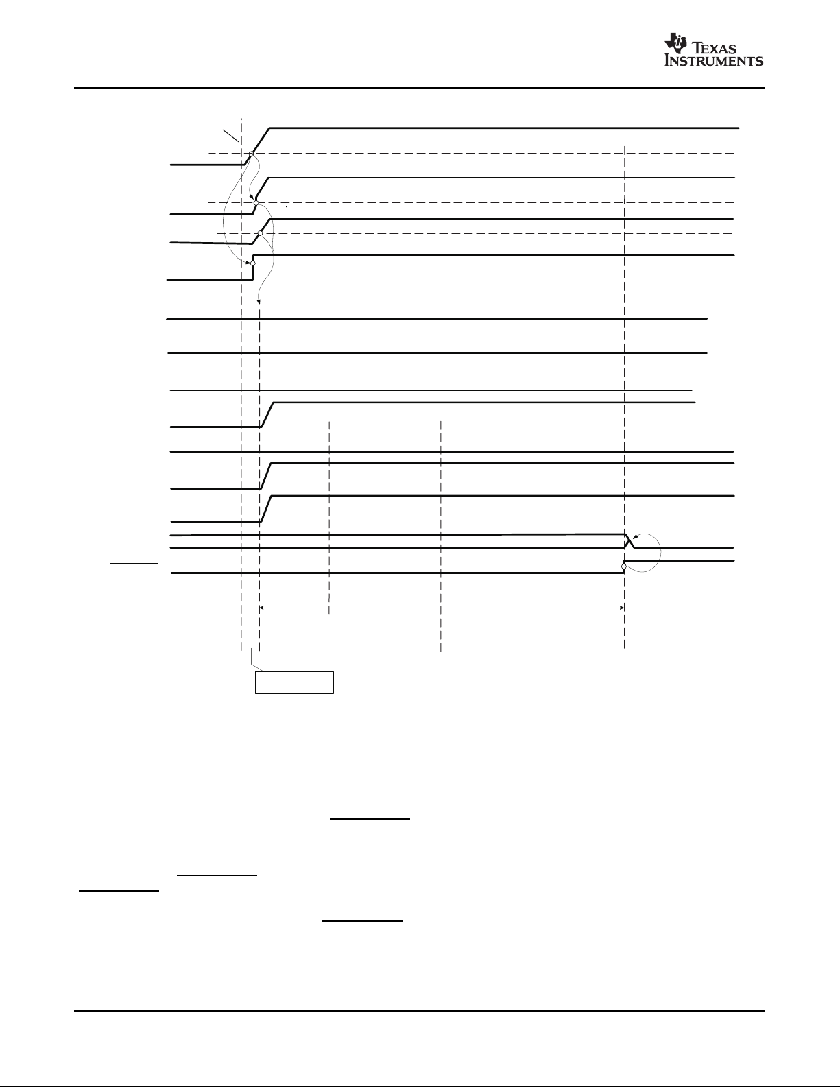
www.ti.com
OUT
RESPWRON
INT
RESET DELAY
PROGRAMMEDBY EXTERNAL CAPACITOR
CONNECTED TOPIN TRSTPWON
Power Applied
SEQUENCING
RESET
NOPOWER
I CRegistersLoaded
FromEEPROM
2
ENABLE
HIGHIMPEDANCE HIGHIMPEDANCEHIGHIMPEDANCE
SeeNote2
NORMAL
AC,USBorBAT
V
UVLO
V
UVLO
V
LOW_SYS
SYS_IN
RTC_OUT
LDO1
LDO2
LDO4
LDO5
LDO3
SM2
SeeNote1
SeeNote1
SM1
TPS65810
TPS65811
SLVS658B – MARCH 2006 – REVISED FEBRUARY 2007
(1) SM1 and SM2 are externally enabled by GPIO1 and GPIO2. This waveform represents the earliest time that SM1 and
SM2 are enabled if GPIO1 and GPIO2 are tied high.
(2) LDO5, SM1, and SM2 are all enabled at the same time. This waveform represents the earliest time that LDO5 is
enabled if VIN_LDO35 is connected to OUT. LDO5 power up can be synchronized to SM1 or SM2 by connecting
VIN_LDO35 to the SM1 or SM2 output, respectively.
Figure 29. TPS65810 Supply Sequencing Timing
RESET – When the reset state starts the RESPWRON output is LO. The user can program the reset timer value
selecting the value of the external capacitor connected to pin TRSTPWON, as shown below:
T
(RESET)
= K
° C
RESET
TRSTPWON
; where K
is the reset timer constant (1 ms/nF typ)
RESET
The TPS65810 RESPWRON pin should be used to reset the external host. During the external host reset
( RESPWRON = LO) the I2C SDA and SCL pins are not used to access TPS65810 internal registers. If a
non-standard configuration is used to reset the system the SDA and SCL lines should not be used to
communicate with the TPS65810 until RESPWRON = HI, in order to avoid overwriting the integrated power
supply internal power-up settings during the sequencing mode.
The power good comparators are masked during the reset mode. The reset mode ends when the reset timer
expires, and the TPS65810 goes into the power good check mode.
36 Submit Documentation Feedback Copyright © 2006 – 2007, Texas Instruments Incorporated
Product Folder Link(s): TPS65810 TPS65811

www.ti.com
TPS65810
TPS65811
SLVS658B – MARCH 2006 – REVISED FEBRUARY 2007
The RESPWRON signal set to a high level is the proper signal to use as an indicator that the device has
transitioned out of the reset state. During the power-up sequence the RESPWRON pin is asserted LOW until the
RESET TIMER expires. The RESET TIME (t
between the TRSTPWON pin and ground.
When the RESPWRON signal is LO, all internal and external interrupts are ignored. As a result, the open-drain
output that asserts the INT pin LO during a NORMAL MODE interrupt request is disabled. The INT pin is then
asserted HI via a pullup resistor that is typically connected to VOUT. After the RESPWRON signal goes HI, the
interrupt controller is given control of the INT pin. Finally, the rising edge of the RESPWRON pin should be used
to indicate the PMIC has transitioned from the RESET STATE to the POWER GOOD CHECK STATE. At that
point, the interrupt controller asserts an interrupt if necessary.
POWER GOOD CHECK – In the power good check mode the power good comparators are enabled, providing
status on the integrated supplies output voltages. An output voltage is considered as out of regulation and
generates a fault condition if the output voltage is below 90% of the target output voltage regulation value. If a
power good fault is detected the SLEEP mode is set, if a power good fault is not detected the NORMAL mode is
set.
The individual supply power good status can be masked via an I2C register PGOODFAULT_MASK. Supplies that
have their power-good fault status masked do not generate a power-good fault. However, the status bit for the
supply indicates that the output voltage is out of regulation.
The power good mask register bits default to masked upon power up.
NORMAL MODE – If a power good fault is not present at the end of the power good check mode the NORMAL
mode starts. In this mode of operation the I2C registers define the TPS65810 operation, and the host has full
control on operation modes, parameter settings, etc. The normal state operation ends if a thermal fault, system
low voltage fault ( V(SYS_IN) < V
LOW_SYS
) or power good fault is detected. A thermal fault or system low voltage
fault sets the SLEEP mode operation, a power good fault sets the NO POWER operation mode. From the normal
mode the converters SM1 and SM2 can be set in the STANDBY mode, with reduced output voltages. In
NORMAL mode either an I2C register bit (SOFT_RESET register bit SOFT_RST) or a hardware input (
HOT_RESET pin set to LO) can trigger a transition to the RESET state, enabling implementation of a host reset
function. In NORMAL mode an I2C register bit (SOFT_RESET register bit SLEEP_MODE) can trigger a transition
to SLEEP mode.
SLEEP MODE – The SLEEP mode is set when a thermal fault or system low voltage fault is detected, under
NORMAL operation mode set. This operation mode is also set when a power good fault is detected during the
power good check state or via the I2C bit SLEEP_MODE. In the SLEEP mode the RESPWRON output is set to
LO, and the I2C registers keep the same contents as in the state preceding SLEEP mode, with the exception of
the following control bits, which are reset to the default power-up values:
1. LDO1,2,3,4,5 and RTC_OUT are enabled, SIM LDO is disabled: EN_LDO register set to default values
2. LDO0 disabled, all GPIO ’ s with no control function assigned: GPIO12, GPIO3 registers set to default values
3. White LED driver is set to OFF: SM3_SET register has all bits set to LO
4. RGB drivers are set to OFF: RGB_FLASH, RGB_RED, RGB_GREEN, RGB_BLUE registers are set to
default values
5. PWM, PWM_LED drivers OFF: PWM, LED_PWM registers are set to default values
6. ADC engine reset to power up default: ADC_SET, ADC_DELAY, ADC_WAIT registers are set to default
values
In SLEEP mode the power path and main internal blocks are still active, but the internal integrated
supply sequencing is disabled. As a result of that, during SLEEP mode ALL integrated supplies (ALL
LDO's, ALL buck Converters) are disabled.
At the end of the SLEEP mode, the sequencer block uses the I2C control register values (which were reset to the
default power-up values) to sequence the integrated power supplies. The SLEEP mode ends when one of the
three following events happens:
1. If SLEEP was set by thermal fault: The SLEEP mode ends only when all external input supplies and battery
pack are removed and a UVLO condition is detected by the TPS65810, setting the NO POWER mode.
2. If SLEEP was set by a system low voltage detection, or I2C bit SLEEP_MODE, only with battery present:
Input power must be connected, setting the TPS65810 in the ENABLE mode. If no input power is inserted,
the battery discharges until the TPS65810 detects a UVLO condition and enters the NO POWER mode.
= 1ms/nF × CTRSTPWON) can be programmed via a capacitor
reset
Copyright © 2006 – 2007, Texas Instruments Incorporated Submit Documentation Feedback 37
Product Folder Link(s): TPS65810 TPS65811

www.ti.com
TPS65810
TPS65811
SLVS658B – MARCH 2006 – REVISED FEBRUARY 2007
3. ) If sleep was set by a system low voltage detection, power good fault or SLEEP_MODE, with battery and
input power present: all external input supplies connected to AC and USB pins must be removed, and then at
least one of them reconnected to the system. The input power cycling triggers a transition from SLEEP mode
to the ENABLE mode.
PROCESSOR STANDBY STATE – This state is set using an I2C register or a GPIO configured as SM1/SM2
standby control. In standby mode operation, the SM1 and SM2 voltages are set to value distinct than the normal
mode output voltage, and SM1/SM2 are set to PFM mode. The standby output voltage is defined in I2C registers
SM1_STANDBY and SM2_STANDBY.
TPS65810 OPERATING MODE CONTROLS
HARDWARE RESET: A dedicated control pin, HOT_RESET, enables implementation of a hardware reset
function. The system reset pin RESPWRON is set to LO when HOT_RESET = LO for a period longer than the
internal deglitch (5mSec typ). The RESET mode is started when the HOT_RESET pin transitions from LO to HI,
as shown in the state diagram. When HOT_RESET = LO all I2C registers are reset to the default power-up
values.
SOFTWARE RESET: The external host can set the TPS65810 in RESET mode using the I2C register
SOFT_RESET, bit B0 (SOFT_RST).
SOFTWARE SLEEP: The external host can set the TPS65810 in SLEEP mode using the I2C register
SOFT_RESET, bit B6 (SLEEP_MODE).
A software reset does not affect the contents of the I2C registers.
SEQUENCING AND OPERATING MODES – I2C REGISTERS
The I2C registers that control sequencing-related functions are shown below. The HEX address for each register
is shown by the register name, together with the R or W functionality for the register bits. Shaded values indicate
default initial power-up values.
SOFT_RESET, ADDRESS=08, ALL BITS R/W, BITS B7/B6/B1/B0 APPLY TO SEQUENCING.
B7 B6 B5 B4 B3 B2 B1 B0
Bit name STBY MODE SLEEP MODE NOT USED NOT USED SM3_LF_OSc NOT USED nRAMLOAD SOFT RST
Function SET SM1 AND SET TPS65810 NOT USED NOT USED NOT RELATED NOT USED RAM RESET SOFTWARE
When 0 NOT ACTIVE NOT ACTIVE NOT USED NOT USED NOT USED RAM NOT ACTIVE
When 1 When 1 SET SET SLEEP NOT USED NOT USED NOT USED RAM SET RESET
Some host algorithms need to identify when the power-up defaults are loaded in the RAM, in order to start
routines that initialize specific RAM registers. If that functionality is required the nRAMLOAD bit should be set to
HI by the host when entering the NORMAL operation mode. The nRAMLOAD bit is reset to LO by the TPS65810
when the power-up defaults are loaded in the I2C registers (V(OUT) < V
enabling the host algorithm to detect that the RAM registers need to be initialized.
The integrated supplies status is available in a dedicated register, shown below. The host can select which
integrated supply outputs trigger a power-good fault condition using the PGOODFAULT_MASK register. When a
non-masked power-good status register bit toggles state, the sequence controller generates a transition in the
TPS65810 state machine, indicated as a PGOOD FAULT in TPS65810 state diagram. The power-good status
register and mask register are shown below:
SYSTEM STATUS MONITORED BY SEQUENCING CONTROLLER
PGOOD, ADDRESS=02, ALL BITS READ ONLY - POWER UP DEFAULTS SHOW SYSTEM STATUS WHEN EXITING POWER DOWN
Bit name PGOOD SM1 PGOOD SM2 PGOOD SM3 PGOOD LDO1 PGOOD LDO2 PGOOD LDO3 PGOOD LDO4 PGOOD LDO5
Function SM1 OUTPUT SM2 SM3 OVP LDO1 OUTPUT LDO2 OUTPUT LDO3 OUTPUT LDO4 OUTPUT LDO5 OUTPUT
SM2 IN IN SLEEP TO FLAG RESET
STANDBY MODE SEQUENCING CONTROL
MODE SEE SM3
SM1 AND SM2 MODE (reset to DEFAULTS MODE (reset to
IN STANDBY LO internally) NOT LOADED LO internally)
B7 B6 B5 B4 B3 B2 B1 B0
STATUS OUTPUT STATUS STATUS STATUS STATUS STATUS STATUS
STATUS
SECTION
DEFAULTS
LOADED
OR V( HOT_RESET) = LO),
UVLO
38 Submit Documentation Feedback Copyright © 2006 – 2007, Texas Instruments Incorporated
Product Folder Link(s): TPS65810 TPS65811

www.ti.com
TPS65810
TPS65811
SLVS658B – MARCH 2006 – REVISED FEBRUARY 2007
SYSTEM STATUS MONITORED BY SEQUENCING CONTROLLER
B7 B6 B5 B4 B3 B2 B1 B0
When 0 OK OK OK OK OK OK OK OK
When 1 FAULT FAULT FAULT FAULT FAULT FAULT FAULT FAULT
PGOODFAULT_MASK, ADDRESS=07, ALL BITS R/W
Bit name MASK_PSM1 MASK_PSM2 MASK_PSM3 MASK_PLDO1 MASK_PLDO2 MASK_PLDO3 MASK_PLDO4 MASK_PLDO5
Function MASK PGOOD MASK MASK PGOOD MASK PGOOD MASK PGOOD MASK PGOOD MASK PGOOD MASK PGOOD
When 0 UNMASKED UNMASKED UNMASKED UNMASKED UNMASKED UNMASKED UNMASKED UNMASKED
When 1 MASKED MASKED MASKED MASKED MASKED MASKED MASKED MASKED
INTERRUPT CONTROLLER
The TPS65810 has internal block and overall system status information stored in I2C status registers. The
following subsystems and system parameters are monitored:
• External power supply status: AC or USB supply detected, AC or USB connected to system, AC/USB OVP
• Charger status: on/off/suspend, fast charge/pre-charge, termination detected, DPPM on, thermal loop ON
• Battery pack status: temperature, discharge on/off
• TPS65810 thermal shutdown
• ADC status: conversion status, input out of range, ANLG1 high impedance detection
• Integrated supplies status: output out of regulation (power good fault)
The GPIO1 and GPIO2 pins can be configured as inputs, generating an interrupt request to the host (
INT:HI → LO) at the GPIO rising or falling edge. The host can use internal the INT_MASK I2C registers to define
which of the monitored status variables triggers an interrupt. When a non-masked system status bit toggles state,
the interrupt controller issues an interrupt, following the steps below:
1. system status bits that caused the interruption are set to HI in registers INT_ACK1 and INT_ACK2
2. An interrupt is sent to the host ( INT:HI → LO)
Once an interrupt is sent to the host, INT is kept in the LO state and the INT_ACK register contents are latched,
holding the system status that generated the currently issued interrupt request. When an interrupt request is
active ( INT = LO) additional changes in non-masked status registers and control signals are ignored, and the
INT_ACK registers are not updated.
The host must write a 0 to the INT_ACK register bit that generated the interrupt in order to set INT = HI and
enable new updates to the INT_ACK registers. If the host stops in the middle of a WRITE or READ operation,
the INT pin stays at the LO level. The TPS65810 has no reset timeout; it is assumed that the host does not leave
INT = LO and the status registers unread for a long time.
The non-masked I2C register bits and internal control signals generate a new interrupt only after INT is set to HI.
The non-masked power-good fault register bits generate a power-good fault when any of the non-masked bits
detects that the monitored output voltage is out of regulation, independently of the INT pin level.
FAULT BY SM1 PGOOD FAULT BY FAULT BY FAULT BY FAULT BY FAULT BY FAULT BY
FAULT BY SM3 LDO1 LDO2 LDO3 LDO4 LDO5
SM2
SYSTEM STATUS — I2C REGISTERS
The I2C registers that have system status data are shown below. The HEX address for each register is shown by
the register name, together with the R or W functionality for the register bits. Those registers are valid, after an
initial power up, when the TPS65810 enters the normal operation mode.
SYSTEM STATUS MONITORED BY INTERRUPT CONTROLLER
B7 B6 B5 B4 B3 B2 B1 B0
PGOOD, ADDRESS=02, ALL BITS READ ONLY - POWER UP DEFAULTS SHOW SYSTEM STATUS WHEN EXITING POWER DOWN
Bit name PGOOD SM1 PGOOD SM2 PGOOD SM3 PGOOD LDO1 PGOOD LDO2 PGOOD LDO3 PGOOD LDO4 PGOOD LDO5
Function SM1 OUTPUT SM2 OUTPUT SM3 OVP LDO1 OUTPUT LDO2 OUTPUT LDO3 OUTPUT LDO4 OUTPUT LDO5 OUTPUT
STATUS STATUS STATUS STATUS STATUS STATUS STATUS STATUS
When 0 OK OK OK OK OK OK OK OK
When 1 FAULT FAULT FAULT FAULT FAULT FAULT FAULT FAULT
ADC STATUS
Copyright © 2006 – 2007, Texas Instruments Incorporated Submit Documentation Feedback 39
Product Folder Link(s): TPS65810 TPS65811
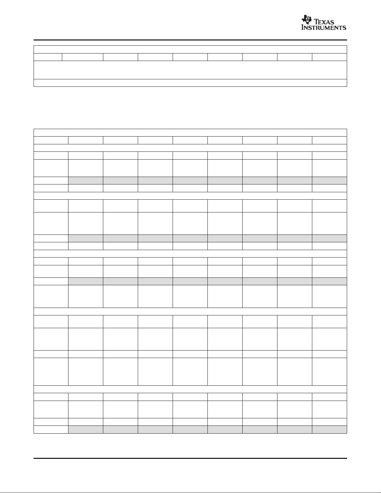
www.ti.com
TPS65810
TPS65811
SLVS658B – MARCH 2006 – REVISED FEBRUARY 2007
SYSTEM STATUS MONITORED BY INTERRUPT CONTROLLER
B7 B6 B5 B4 B3 B2 B1 B0
REGISTER ADC_READING_HI, B7: CONVERSION COMPLETE;
INTERNAL STATUS BITS (NO I2C REGISTER BIT AVAILABLE: INPUT OUT OF RANGE (HI OR LO), ANLG1 PIN IMPEDANCE TO AGND2 EXCEEDS 1 m Ω .
See additional details in the Analog-to-Digital Converter section.
OTHER SYSTEM STATUS: THERMAL FAULT DETECTED
INTERRUPT CONTROLLER – I2C REGISTERS
The I2C registers that control an interrupt generation (INT: HI → LO) are shown below. The HEX address for each
register is shown by the register name, together with the R or W functionality for the register bits. Shaded values
indicate default initial power-up values.
INTERRUPT AND POWER GOOD FAULT MANAGEMENT REGISTERS
B7 B6 B5 B4 B3 B2 B1 B0
INTMASK1, ADDRESS=03, ALL BITS R/W
Bit name MASK_ISM1 MASK_ISM2 MASK_ISM3 MASK_ILDO1 MASK_ILDO2 MASK_ILDO3 MASK_ILDO4 MASK_ILDO5
Function MASK INT by MASK INT by MASK INT by MASK INT by MASK INT by Mask INT by MASK INT by MASK INT by
When 0 UNMASKED UNMASKED UNMASKED UNMASKED UNMASKED UNMASKED UNMASKED UNMASKED
When 1 MASKED MASKED MASKED MASKED MASKED MASKED MASKED MASKED
INTMASK2, ADDRESS=04, ALL BITS R/W
Bit name MASK_IADC MASK_IANLG1 MASK_IGPIO2 MASK_IGPIO1 MASK_ITHSHU MASK_ICHGS MASK_IADC_H MASK_IADC_L
Function MASKS INT BY MASKS INT BY MASKS INT BY MASKS INT BY MASKS INT BY MASK INT BY MASK INT BY MASK INT BY
When 0 UNMASKED UNMASKED UNMASKED UNMASKED UNMASKED UNMASKED UNMASKED UNMASKED
When 1 MASKED MASKED MASKED MASKED MASKED MASKED MASKED MASKED
INT_ACK1, ADDRESS=05, ALL BITS R/W
Bit name ACK_SM1 ACK_SM2 ACK_SM3 ACK_LDO1 ACK_LDO2 ACK_LDO3 ACK_LDO4 ACK_LDO5
Function SM1 INT SM2 INT SM3 INT LDO1 INT LDO2 INT LDO3 INT LDO4 INT LDO5 INT
When 0 CLEAR FLAG CLEAR FLAG CLEAR FLAG CLEAR FLAG CLEAR FLAG CLEAR FLAG CLEAR FLAG CLEAR FLAG
When 1 SM1 PGOOD SM2 PGOOD SM3 OVP LDO1 PGOOD LDO2 PGOOD LDO3 PGOOD LDO4 PGOOD LDO5 PGOOD
INT_ACK2, ADDRESS=06, ALL BITS READ ONLY
Bit name ACK_ADC ACK_ANLG1 ACK_GPIO2 ACK_GPIO1 ACK_THSHUT ACK_CHGSTA ACK_ADC_HI ACK_ADC_LO
Function ADC INT ANLG1 GPIO2 INT GPIO1 INT THERMAL CHARGER INT ADC INT ADC INT
When 0 CLEAR FLAG CLEAR FLAG CLEAR FLAG CLEAR FLAG CLEAR FLAG CLEAR FLAG CLEAR FLAG CLEAR FLAG
When 1 ADC DONE ANLG1 HIGH GPIO2 EDGE GPIO1 EDGE THERMAL CHARGER ADC INPUT ADC INPUT
PGOODFAULT_MASK, ADDRESS=07, ALL BITS R/W
Bit name PGOOD SM1 PGOOD SM2 PGOOD SM3 PGOOD LDO1 PGOOD LDO2 PGOOD LDO3 PGOOD LDO4 PGOOD LDO5
Function MASK PGOOD MASK PGOOD MASK PGOOD MASK PGOOD MASK PGOOD MASK PGOOD MASK PGOOD MASK PGOOD
When 0 UNMASKED UNMASKED UNMASKED UNMASKED UNMASKED UNMASKED UNMASKED UNMASKED
When 1 MASKED MASKED MASKED MASKED MASKED MASKED MASKED MASKED
SM1 PGOOD SM2 PGOOD SM3 PGOOD LDO1 PGOOD LDO2 PGOOD LDO3 PGOOD LDO4 PGOOD LDO5 PGOOD
FAULT FAULT FAULT FAULT FAULT FAULT FAULT FAULT
T T I O
ADC END OF ANLG1 HIGH GPIO2 EDGE GPIO1 EDGE THERMAL CHG_STAT ADC INPUT ADC INPUT
CONVERSION IMPEDANCE TRANSITION TRANSITION FAULT REGISTER ABOVE HI BELOW LO
BITS LIMIT LIMIT
REQUEST REQUEST REQUEST REQUEST REQUEST REQUEST REQUEST REQUEST
FAULT FAULT FAULT FAULT FAULT FAULT FAULT FAULT
GENERATED GENERATED GENERATED GENERATED GENERATED GENERATED GENERATED GENERATED
INT INT INT INT INT INT INT INT
T
REQUEST 1 COMPARATO REQUEST REQUEST FAULT INT REQUEST REQUEST 2 REQUEST 3
R INT REQUEST
REQUEST
GENERATED IMPEDANCE GENERATED GENERATED FAULT STATUS ABOVE HI BELOW LO
INT REQUEST DETECTION INT REQUEST INT REQUEST GENERATED CHANGE LIMIT LIMIT
GENERATED INT REQUEST GENERATED GENERATED GENERATED
INT REQUEST INT REQUEST INT REQUEST INT REQUEST
FAULT BY FAULT BY FAULT BY FAULT BY FAULT BY FAULT BY FAULT BY FAULT BY
SM1 SM2 SM3 LDO1 LDO2 LDO3 LDO4 LDO5
40 Submit Documentation Feedback Copyright © 2006 – 2007, Texas Instruments Incorporated
Product Folder Link(s): TPS65810 TPS65811

www.ti.com
AC
BAT
OUT
USB
TMR
ISET
1
TS
BAT
OUT
DPPM
POWERPATH
CONTROL
LINEAR
CHARGER
Battery
GND
+
-
AC _DC Adapter
Output
USBPower
ACSWITCH
USBSWITCH
BATTERY
SWITCH
SYSTEMPOWERBUS
TPS 65810
Withtheabovecomponentsthefollowingsystem
parametersareset :
FastChargeCurrent = 1A (100% scaling, inputlimit=2.5A)
Safety Timer = 5hours, 30 minpre-charge
DPPMthreshold = 4.3V
Temphot: 65C
TempCold : 5C
SystemPower
Selection
InputCurrentLimit
Selection
ChargeVoltage
FastCharge
CurrentScaling
ChargeSuspend
I2CREGISTERS
R
37.4k
DPPM
W
A1
C26
22 Fm
C25
10 Fm
50k
NTC
W
R
49.9k
TMR
W
C2
10 Fm
C23
47nF
A1
R
1k
SET
W
A1
C24
0.22 Fm
A1
C1
10 Fm
TPS65810
TPS65811
SLVS658B – MARCH 2006 – REVISED FEBRUARY 2007
FUNCTIONALITY GUIDE — SYSTEM POWER AND CHARGE MANAGEMENT
Fast Charge
Charge Charge Current Current Current Scaling
(1)
Precharge Termination Charge Precharge SafetyTimer Power Up
Current Voltage Voltage Timeout Default
Current Value Scaling
I
, 25%, 50%, 75%, 10% of I(TERM), 10% of 25%, 50%, 75%, 4.2 V or 3.0 V Programmable Charger OFF
O(BAT)
Programmable, 100% of I
1.5A max value
Set via external Fixed ratio Fixed ratio Fixed Set via external
resistor resistor
O(BAT)
Set via I2C Set via I2C Set via I2C
I
O(BAT)
(1) The input current limit (see system power management below ) regulates the input current, effectively limiting the charge current if the
input current limit is lower than the fast charge current value programmed.
INPUT CURRENT LIMIT INPUT CONNECTED TO OUT PIN POWER UP DEFAULT
AC PIN USB PIN INPUT POWER TO SYSTEM BATTERY TO SYSTEM
2.5 A typ 100 mA max or #1 – AC Battery connected to system, Input Power to System,
Internal fixed Automatic internal algorithm
current limit
500 mA max or #2 – USB independently of battery USB mode selected,
2.5 A typ #3 – Battery (when AC pin power and USB pin power are voltage 100 mA max
not detected )
Set via I2C Set via I2C, overrides
CHARGE MANAGEMENT
I
O(BAT)
100% of I
(TERM)
4.36 V
POWER PATH MANAGEMENT
internal algorithm
Figure 30. Required External Components, Recommended Values, External Connections
POWER PATH AND CHARGE MANAGEMENT
Overview
The TPS65810 has an integrated charger with power path integrated MOSFETs. This topology, shown in the
simplified block diagram below, enables using an external input power to run the system and charge the battery
simultaneously. The power path has dual inputs that can be used to select either an external AC_DC adapter
(AC pin) or an USB port power (USB pin) to power the end equipment main power rail (OUT pin, also referred to
as the system power bus) and charge the battery pack (connected to BAT pin).
Copyright © 2006 – 2007, Texas Instruments Incorporated Submit Documentation Feedback 41
Product Folder Link(s): TPS65810 TPS65811
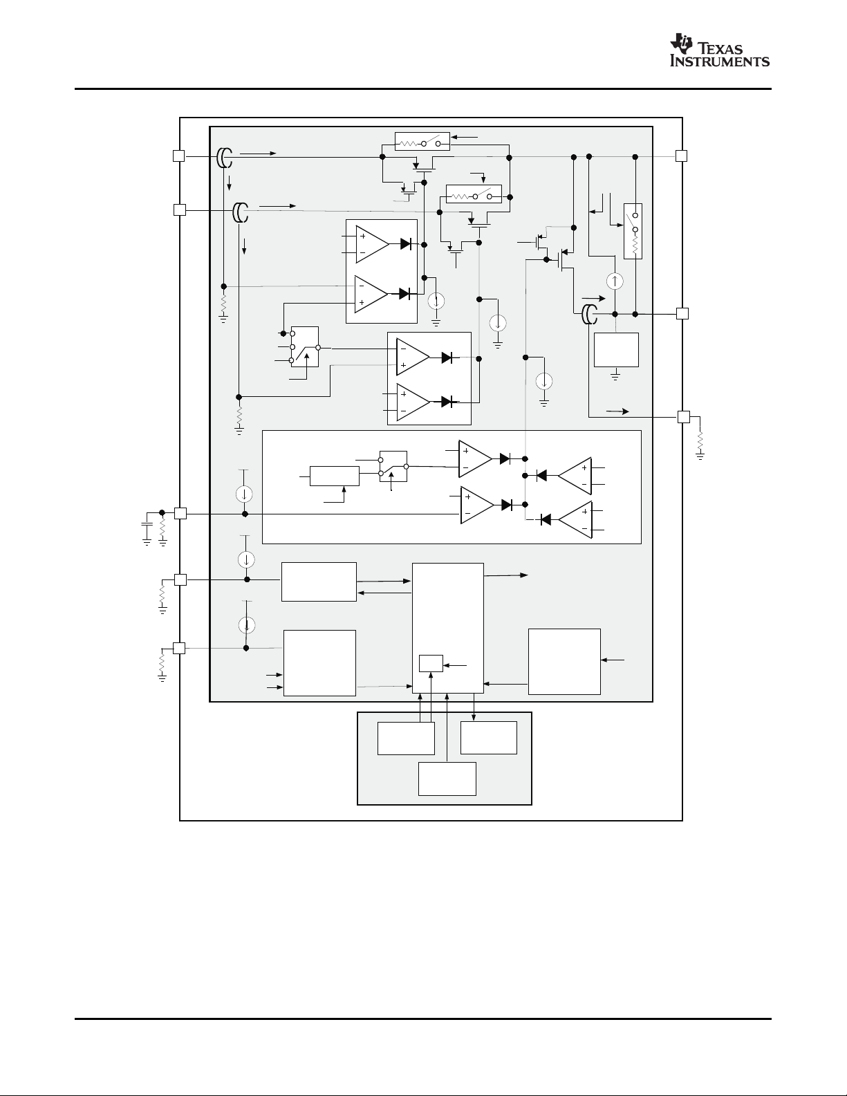
www.ti.com
BAT
BATTERY
STATUS
ISET1
CHARGE
CONTROL AND
POWERPATH
MANAGEMENT
VREF
I( )
I(OUT)/ K
(SET)
TS
OUT
V
(DPPM)
DPPM
V
(SET)
V(ISET1)
V
(PRECHG)
CHMODE
V
(USB2)
INPUT_LIM
V
(USB1)
V
(ACOC)
V(OUT)
V
O(REG)
V(OUT)
V
O(REG)
T
J(REG)
T
J
V(BAT)
V
O(REG)
BATTERY
STATUS
DETECTION
SYSTEM
STATUS
DETECTION
Dynamically
Controlled
Oscillator
TimerFault
VREF
USB
AC
SCALING
ATTENUATION
CONTROL SIGNALS
BATOFF
USBOFF
ACOFF
TMR
OUT
USB
AC
BAT
On, Reset
SystemPower
Selection
InputCurrentLimit
Selection
ChargeVoltage
FastCharge
CurrentScaling
ChargeSuspend
ChargerStatus
InputPowerStatus
ChargerControlLoops
Charge
Current
Loop
DPPM
Loop
Thermal
Loop
ChargeVoltage
Loop
USBControlLoops
USBInputCurrent
LimitLoop
ACInputCurrent
LimitLoop
SystemVoltage
RegulationLoop
SystemVoltage
RegulationLoop
ACControlLoops
ACSWITCH
BATTERY
SWITCH
USBSWITCH
I2C
REGISTERS
TPS65810
I(AC)/ K
INTAC
I(USB)/ K
INTUSB
I(AC)
I(USB)
CE
LATCH
CHG_UVLO
CE
500Ω
500
OUTSHORT
OUTSHORT
BATSHORT
VREF
ISET1
SYSTEM
STATUS
BAT
DISCHARGE
CIRCUIT
1k
Ω
BAT
TPS65810
TPS65811
SLVS658B – MARCH 2006 – REVISED FEBRUARY 2007
Figure 31. TPS65810 Charger and Power Path Section Simplified Block Diagram
The power path has three integrated power MOSFETs: the battery to system MOSFET (battery switch), the AC
input to system MOSFET (AC switch) and the USB input to system MOSFET (USB switch). Each of those power
MOSFETs can be operated either as an ON/OFF switch or as a linear pass element under distinct operating
conditions, as defined by the control circuits that set the power MOSFET gate voltage.
42 Submit Documentation Feedback Copyright © 2006 – 2007, Texas Instruments Incorporated
Product Folder Link(s): TPS65810 TPS65811

www.ti.com
POWERPATH
CONTROL LOGIC
ACDETECTED
USBDETECTED
USBOVP
ACOVP
OUT SHORTED
BAT
SHORTED
OUT LOWER
THANBAT
V
BATSH
AC
USB
OUT
BAT
V
OVP
V
OVP
BAT
V
OUTSH
BAT
OUT
BAT
NOBATT
SHORT
DPPM
1V
TPS65810
TPS65811
SLVS658B – MARCH 2006 – REVISED FEBRUARY 2007
The TPS65810 regulates the voltage at the OUT pin to 4.6 V when one of the external supplies connected to
pins AC or USB is powering the OUT pin. The selected input (AC or USB pin) current is limited to a value defined
by I2C register settings. The input current limit function assures compatibility with USB standard requirements,
and also implements a protection function by limiting the maximum current supplied by an external AC_DC
adapter or USB port power terminal.
The AC power MOSFET and USB power MOSFET operating modes are set by integrated control loops. Each of
the power MOSFETs is controlled by two loops: one system voltage regulation loop and one input current limiting
loop. The integrated loops modulate the AC or USB power MOSFETs drain to source resistance to regulate
either the OUT pin voltage or to limit the input current. If no input power is present (AC and USB input power not
detected) the AC and USB power MOSFETs are turned OFF, and the battery MOSFET is turned ON, connecting
the BAT pin to the OUT pin.
The battery switch is turned ON when the AC or USB input power is detected and the charger function is
enabled, charging the battery pack. During charge the battery MOSFET switch operation mode is defined by the
charger control loops. The battery MOSFET switch drain-to-source resistance is modulated by the charge current
loop and charge voltage loop in order to implement the battery charging algorithm. In addition to that multiple
safety functions are activated (thermal shutdown, safety timers, short circuit recovery), and additional functions
(thermal loop and DPPM loop) optimize the charging process.
POWER PATH MANAGEMENT FUNCTION
Detecting the System Status
The power path and charge management block operate independently of the other TPS65810 circuits. Internal
circuits check battery parameters (pack temperature, battery voltage, charge current) and system parameters
(AC and USB voltage, battery voltage detection), setting the power path MOSFETs operating modes
automatically. The TPS65810 has integrated comparators that monitor the battery voltage, AC pin voltage, USB
pin voltage and the OUT pin voltage. The data generated by those comparators is used by the power path
control logic to define which of the integrated power path switches are active. A simplified block diagram for the
system status detection is shown below.
Table 4 lists the system power detection conditions. V
references, refer to the electrical characteristics for additional details.
Copyright © 2006 – 2007, Texas Instruments Incorporated Submit Documentation Feedback 43
Figure 32. TPS65810 Systems Status Detection, Charger and Power Path Section
Product Folder Link(s): TPS65810 TPS65811
, V
IN(DT)
, V
OUTSH
, V
BATSH
OVP
are TPS65810 internal

www.ti.com
TPS65810
TPS65811
SLVS658B – MARCH 2006 – REVISED FEBRUARY 2007
Table 4. System Status Detection, Charger and Power Path Section
AC input voltage detected V(AC) – V(BAT) > V
USB input voltage detected V(USB) – V(BAT) > V
AC overvoltage detected V(AC) > V
USB overvoltage detected V(USB) > V
AC PIN TO OUT pin OR USB TO OUT PIN short detected V(OUT) < V
BAT pin to OUT pin short detected V(BAT) - V(OUT) > V
Battery supplement mode need detected V(BAT) – V(OUT) > V
Blank BAT to OUT short circuit detection V(DPPM) < 1V
OVP
OVP
Power Path Logic: Priority Algorithm
The system power bus supply is automatically selected by the power path control logic, following an internal
algorithm. The power path function detects an external input power connection when the input voltage exceeds
the battery pack voltage. It also detects a supplement mode need (battery switch must be turned ON) when the
system voltage (OUT pin) is below the battery voltage. A connected and non-selected external supply or the
battery is automatically switched to the system bus, following the priority algorithm, when the external supply
currently selected is disconnected from the system.
The input power priority is hard-wired internally, with the AC input having the higher priority, followed by the USB
input (2
nd
) and the battery pack (3
rd
). Using the I2C CHG_CONFIG register control bit CE the user can override
the power path algorithm, connecting the battery to the system power bus. Care must be taken when using the
battery-to-system connection option, as the system power bus is not connected back to the AC or USB inputs
(even if those are detected) when the battery is removed. Table 5 describes the priority algorithm.
IN(DT)
IN(DT)
INOUTSH
BATOUTSH
SUP
Table 5. Power Path Control Logic Priority Algorithm
(I2C CHG_CONFIG Register) DETECTED SOURCE
CE BIT EXTERNAL SUPPLY SWITCH MODE SYSTEM POWER
AC USB AC USB Battery
HI YES NO ON OFF ON if Supplement mode is AC
NO YES OFF ON USB
YES YES ON OFF AC
NO NO OFF OFF BATTERY
LO XX XX OFF OFF ON BATTERY
required, OFF otherwise
The power path status is stored in register CHG_STAT.
Input Current Limit
The USB input current is limited to the maximum value programmed by the host, using the I2C interface. If the
system current requirements exceed the input current limit, the output voltage collapses, the charge current is
reduced, and finally, the supplement mode is set. The input current limit value is set with the I2C charge control
register bits PSEL and ISET2, and it is applied to the USB input ONLY. The AC input current limit is fixed to the
internal short circuit limit value.
Table 6. Charge Current Scaling via I2C
PSEL (I2C) ISET2 (I2C) INPUT CURRENT LIMIT
USB AC
LO LO 100 mA 2.75 A
LO HI 500 mA 2.75 A
HI LO 2.75 A 2.75 A
HI HI 2.75 A 2.75 A
44 Submit Documentation Feedback Copyright © 2006 – 2007, Texas Instruments Incorporated
Product Folder Link(s): TPS65810 TPS65811

www.ti.com
BAT
OUT
V -V
(OUT) (NOBATID)
+
_
ANLG1
Battery
I C
2
TPS65810
PACKID
Resistor
TPS65810
TPS65811
SLVS658B – MARCH 2006 – REVISED FEBRUARY 2007
System Voltage Regulation
The system voltage is regulated to a fixed voltage when one of the input power supplies is connected to the
system. The system voltage regulation is implemented by a control loop that modulates the selected switch
Rds(on).
The typical system regulation voltage is 4.6 V.
Input Overvoltage Detection
The AC and USB input voltages are monitored by voltage comparators that identify an overvoltage condition. If
an overvoltage condition is detected a status register bit is set, indicating a potential fault condition.
When an overvoltage condition is detected, the AC or USB switches state is not modified. If any of those
switches was ON, it is kept in the ON state. During overvoltage conditions, the system voltage is still regulated,
and no major safety issues are observed when not modifying the input switch state.
If the input overvoltage condition results in excessive power dissipation, the thermal shutdown circuit is activated,
the AC and USB switches are turned OFF, and the BAT switch is turned ON.
Output Short-Circuit Detection
If the OUT pin voltage falls below an internal threshold V
INOUTSH
internal pullup resistors are connected from AC pin to OUT pin and USB pin to OUT pin. When the short circuit is
removed those resistors enable the OUT pin voltage to rise above the V
normal operation.
the AC and USB switches are turned off and
INOUTSH
threshold, returning the system to
Battery Short-Circuit Detection
If the OUT pin voltage falls below the BAT pin voltage by more than an internal threshold V
BATOUTSH
the battery
switch is turned off and internal pullup resistor is connected between the OUT pin and the BAT pin. This resistor
enables detection of the short removal, returning the system to normal operation.
Initial Power Path Operation
During the initial TPS65810 power-up the contents of the ISET2, CE and SUSPEND bits on the control register
are immediately implemented. The charger is disabled (SUSPEND=LO) and the selected input current limit is set
internally to 500 mA max.
No-Battery Detection Circuit
The ANLG1 pin may be used to detect the connection of an external resistor that is embedded in a battery pack
and is used as a pack ID function. The ANLG1 pin has an internal current source connected between OUT and
ANLG1, which is automatically enabled when the TPS65810 is not in SLEEP mode. The current levels for
ANLG1 pin can be programmed via I2C register ADC_WAIT, bits BATID_n, as shown below:
Copyright © 2006 – 2007, Texas Instruments Incorporated Submit Documentation Feedback 45
Figure 33. Battery Removal Detection, ANLG1 Pin
Product Folder Link(s): TPS65810 TPS65811

www.ti.com
TPS65810
TPS65811
SLVS658B – MARCH 2006 – REVISED FEBRUARY 2007
An internal comparator with a fixed deglitch time, t
V(OUT) - V
NOBATID
a battery removed condition is detected and an internal discharge switch is activated,
DGL(NOBAT)
monitors the ANLG1 pin voltage, if V(ANLG1) >
connecting an internal resistor from BAT pin to AGND1. Note that ANLG1 can also be used as an analog input
for the ADC converter, in this case the voltage at pin ANLG1 must never exceed the V(OUT) - V
NOBATID
threshold
to avoid undesired battery discharge.
Using the Input Power to Run the System and Charge the Battery Pack
The external supply connected to AC or USB pins must be capable of supplying the system power and the
charger current. If the external supply power is not sufficient to run the system and charge the battery pack the
TPS65810 executes a two-stage algorithm that prevents a low voltage condition at the system power bus:
1. The charge current is reduced, until the total (charger + system current) is at a level that can be supplied by
the external input supply. This function is implemented by a dedicated charger control loop (see DPPM
section in charger functional description for additional details).
2. The battery switch is turned ON if the charge current is reduced to zero and the input current is not enough
to run the system. In this mode of operation both the battery and the external input power supply the system
power ( supplement operation mode).
The supplement operation mode is automatically set by the TPS65810 when the input power is switched to the
OUT pin, and the OUT pin voltage falls below the battery voltage.
BATTERY CHARGE MANAGEMENT FUNCTION
Operating Modes
The TPS65810 supports charging of single-cell Li-Ion or Li-Pol battery packs. The charge process is executed in
three phases: pre-charge (or pre-conditioning), constant current and constant voltage.
The charge parameters are selectable via I2C interface and using external components. The charge process
starts when an external input power is connected to the system, the charger is enabled by the I2C register
CHG_CONFIG bits CE=HI and CHGON=HI, and the battery voltage is below the recharge threshold, V(BAT) <
V
. When the charge cycle starts a safety timer is activated. The safety timer timeout value is set by an
(RCH)
external resistor connected to the TMR pin.
When the charger is enabled two control loops modulate the battery switch drain to source impedance to limit the
BAT pin current to the programmed charge current value (charge current loop) or to regulate the BAT pin voltage
to the programmed charge voltage value (charge voltage loop). If V(BAT) < 3 V (typ) the BAT pin current is
internally set to 10% of the programmed charge current value. A typical charge profile is shown below, for an
operation condition that does not cause the IC junction temperature to exceed 125 ° C (typ).
46 Submit Documentation Feedback Copyright © 2006 – 2007, Texas Instruments Incorporated
Product Folder Link(s): TPS65810 TPS65811
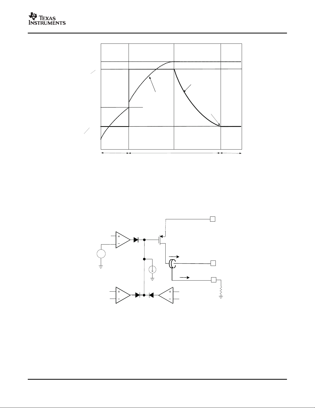
www.ti.com
Batteryvoltage,
V(BAT)
Charge
Complete
Status,
Charger
Off
Pre-
conditioning
Phase
Current
Regulation
Phase
VoltageRegulationand
ChargeTermination
Phase
PRE-CHARGE
CURRENT AND
TERMINATION
THRESHOLD
BatteryCurrent,
I(BAT)
V
O(BATREG)
V
(LOWV)
T
(PRECHG)
T
(CHG)
FAST-CHARGE
CURRENT
I
O(BAT)
I
O(PRECHG),I(TERM)
DONE
DONE
BAT
ISET 1
I /K
(OUT) (SET)
OUT
ChargeVoltage
Loop
Battery
Switch
SystemVoltage
RegulationLoop
VREF
Thermal
Loop
VTJ
V
(OUT)
I
(BAT)
V
(BAT)
V
O(REG)
V
O(REG)
Figure 34. Typical Charge Cycle, Thermal Loop not Active
TPS65810
TPS65811
SLVS658B – MARCH 2006 – REVISED FEBRUARY 2007
If the operating conditions cause the IC junction temperature to exceed 125 ° C the charge cycle is modified, with
the activation of the integrated thermal control loop. The thermal control loop is activated when an internal
voltage reference, which is inversely proportional to the IC junction temperature, is lower than a fixed,
temperature stable internal voltage. The thermal loop overrides the other charger control loops and reduces the
charge current until the IC junction temperature returns to 125 ° C, effectively regulating the IC junction
temperature.
Copyright © 2006 – 2007, Texas Instruments Incorporated Submit Documentation Feedback 47
Product Folder Link(s): TPS65810 TPS65811

www.ti.com
Battery
Voltage,
V(BAT)
Charge
Complete
Status,
Charger
Off
Pre-
conditioning
Phase
Current
Regulation
Phase
VoltageRegulationand
ChargeTermination
Phase
PRE-CHARGE
CURRENT AND
TERMINATION
THRESHOLD
BatteryCurrent,
I(BAT)
V
O(BATREG)
V
(LOWV)
T
(PRECHG)
T
(CHG)
FAST-CHARGE
CURRENT
I
O(BAT)
I
O(PRECHG),I(TERM)
DONE
DONE
Thermal
Regulation
Phase
ICJunction
Temperature, Tj
T
(THREG)
I
O(PRECHG)
+
V
PRECHG
K
SET
R
SET
I
O(BAT)
+
V
SET
K
SET
R
SET
TPS65810
TPS65811
SLVS658B – MARCH 2006 – REVISED FEBRUARY 2007
A modified charge cycle, with the thermal loop active, is shown here:
Figure 35. Typical Charge Cycle, Thermal Loop Active
Battery Preconditioning
The TPS65810 applies a pre-charge current I
o(PRECHG)
to the battery if the battery voltage is below the V
threshold, pre-conditioning deeply discharged cells. The charge current loop regulates the ISET1 pin voltage to
an internal reference value, V
PRECHG
. The resistor connected between the ISET1 and AGND pins, R
determines the precharge rate.
The pre-charge rate programmed by R
is always applied to a deeply discharged battery pack, independently
SET
of the input power selection (AC or USB). The pre-charge current can be calculated as follows:
where:
K
is the charge current scaling factor and V
SET
PRECHG
is the pre-charge set voltage.
CONSTANT CURRENT CHARGING
The constant charge current mode (fast charge) is set when the battery voltage is higher than the pre-charge
voltage threshold. The charge current loop regulates the ISET1 pin voltage to an internal reference value, V
The fast charge current regulation point is defined by the external resistor connected to the ISET1 pin, R
shown in the following:
where:
V
(2.5 V typ) is the voltage at ISET1 pin during charge current regulation and K
SET
Scaling Factor.
The reference voltage V
be selected as a percentage (75%, 50% or 25%) of the original 2.5 V typ, non-attenuated V
can be reduced via I2C register CHG_CONFIG bits ISET1_1 and ISET1_0. V
SET
SET
SET
= Charge Current
value, effectively
scaling down the charge current.
(LOWV)
,
SET
(2)
.
SET
, as
SET
(3)
can
SET
48 Submit Documentation Feedback Copyright © 2006 – 2007, Texas Instruments Incorporated
Product Folder Link(s): TPS65810 TPS65811
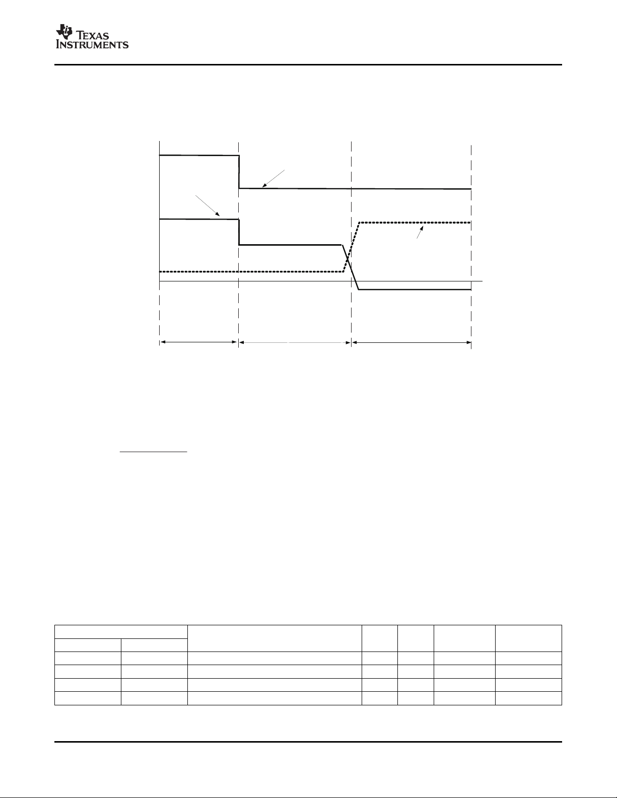
www.ti.com
2.75 A
500 mA
200 mA
750 mA
800 mA
300 mA
-250 mA
SYSTEMLOAD
INPUT
CURRENT
BATTERY
CHARGE
CURRENT
BATTERY
CHARGING,
USBINPUT LIMIT
SET TO 2.75 A
BATTERY
CHARGING,
INPUT LIMIT SET
TO 500 mA
BATTERY
DISCHARGING,
SUPPLEMENT
MODESET
(800mA DEFINED
BY RSET VALUE)
I(USB)
I(OUT )
I
TERM
+
V
TERM
K
SET
R
SET
TPS65810
TPS65811
SLVS658B – MARCH 2006 – REVISED FEBRUARY 2007
The ISET1 resistor always sets the maximum charge current if the AC input is selected. When the USB input is
selected, the maximum charge current is defined by the USB input current limit and the programmed charge
current. If the USB input current limit is lower than the I
and the charge current is defined by the input current limit value and system load, as shown in the following
curves:
value, the battery switch is set in the dropout region
O(OUT)
Figure 36. Input Current Limit Impact on Effective Charge Current
CHARGE TERMINATION AND RECHARGE
The TPS65810 monitors the charging current during the voltage regulation phase. Charge is terminated when
the charge current is lower than an internal threshold, set to 10% (typ) of the fast charge current rate. The
termination point applies to both AC and USB charging, and it can be calculated as follows:
where
V
is the termination detection voltage reference.
TERM
The voltage at ISET1 pin is monitored to detect termination, and termination is detected when V(SET1) < V
(0.25 V typ). The voltage reference V
if the reference voltage V
is scaled via I2C register CHG_CONFIG bits ISET1_1 and ISET1_0. V
SET
reduced by the same percentage used to scale down V
is internally set to 10% of the V
TERM
SET
reference voltage, and it is modified
SET
.
The table below shows charge current and termination thresholds for a 1-A charge current set (1-k Ω resistor
connected to ISET1 pin), with the selected input current limit set to a value higher than the programmed charge
current. The termination current is scaled for all charge current modes (AC or USB), as it is always set by the
ISET1 pin external resistor value.
Table 7. Charge Current and Termination Threshold Selection Example
programmed by ISET1 resistor) (V) (mV) Current (A) Current (mA)
Charge Control Register Bits Charge Current, (% of typical value Vset Vterm Charge Termination
ISET1_1 ISET1_0
0 0 25% 0.6 60 0.24 20
0 1 50% 1.25 115 0.5 40
1 0 75% 1.9 160 0.78 60
1 1 100% 2.5 250 1 100
(4)
TERM
is
TERM
Copyright © 2006 – 2007, Texas Instruments Incorporated Submit Documentation Feedback 49
Product Folder Link(s): TPS65810 TPS65811

www.ti.com
V
DPPM
+ R
DPPM
K
DPPM
I
DPPM
TPS65810
TPS65811
SLVS658B – MARCH 2006 – REVISED FEBRUARY 2007
Once termination is detected, a new charge cycle starts if the voltage on the BAT pin falls below the V
(RCH)
threshold. A new charge start is also triggered if the charger is enabled/disabled/enabled via I2C (CHG_CONFIG
register bits CE or CHGON), or if both AC and USB input power are removed and then at least one of them is
re-inserted.
The termination is disabled when the thermal loop OR DPPM loop are active, and during supplement mode.
BATTERY VOLTAGE REGULATION, CHARGE VOLTAGE
The voltage regulation feedback is Implemented by sensing the BAT pin voltage, which is connected to the
positive side of the battery pack. The TPS65810 monitors the battery-pack voltage between the BAT and AGND1
pins, when the battery voltage rises to the V
O(REG)
threshold the voltage regulation phase begins and the
charging current tapers down.
The charging voltage can be selected as 4.2 V or 4.365 V (typ). The default power-up voltage is 4.2 V. As a
safety measure the 4.365 V charge voltage is programmed only if two distinct bits are set via I2C: VCHG=HI in
the CHG_CONFIG, and CHG_VLTG=LO in the GPIO3 register.
TEMPERATURE QUALIFICATION
The TPS65810 charger section does not monitor the battery temperature. This function may be implemented by
an external host, which can measure the pack temperature by monitoring the ADC channel connected to the TS
pin. An external pullup resistor should be connected to the TS pin in order to bias the pack thermistor, as the
TPS65810 has no internal current source connected to the TS pin.
DYNAMIC POWER PATH MANAGEMENT
Under normal operating conditions, the OUT pin voltage is regulated when the AC or USB pin is powering the
OUT pin and the battery pack is being charged. If the total (system + charge current) exceeds the available input
current, the system voltage drops below the regulation value.
The dynamic power path management function monitors the system output voltage. A condition where the
external input supply rating has been exceeded or the input current limit has been reached is detected when the
OUT pin voltage drops below an user-defined threshold, V
:
DPPM
(5)
where:
R
K
I
= external resistor connected to DPPM pin
DPPM
= DPPM scaling factor
DPPM
= DPPM pin internal current source
DPPM
To correct this situation the DPPM loop reduces the charge current, regulating the OUT pin voltage to the
user-defined V
threshold. The DPPM loop effectively identifies the maximum current that can be delivered by
DPPM
the selected input and dynamically adjusts the charge current to guarantee that the end equipment is always
powered. In order to minimize OUT voltage ripple during DPPM operation the V
threshold should be set just
DPPM
below the system regulation voltage.
If the charge current is reduced to zero by the DPPM and the input current is still lower than the OUT pin load,
the output voltage falls below the DPPM threshold, decreasing until the battery supplement mode is set [V(OUT)
= V(BAT) – V
SUP(DT)
].
CHARGER OFF MODE
The TPS65810 charger circuitry enters the low-power OFF mode if both AC and USB power are not detected.
This feature prevents draining the battery during the absence of input supply.
PRE-CHARGE SAFETY TIMER
The TPS65810 activates an internal safety timer during the battery pre-conditioning phase. The pre-charge
safety timer time-out value is set by the external resistor connected to TMR pin, RTMR, and the timeout
constants K
T
PRECHG
and K
PRE
= K
PRE
:
TMR
× R
× K
TMR
TMR
50 Submit Documentation Feedback Copyright © 2006 – 2007, Texas Instruments Incorporated
Product Folder Link(s): TPS65810 TPS65811

www.ti.com
TPS65810
TPS65811
SLVS658B – MARCH 2006 – REVISED FEBRUARY 2007
The K
constant typical value is 0.1, setting the pre-charge timer value to 10% of the charge safety timer value.
PRE
When the charger is in suspend mode, set via I2C register CHG_CONFIG bit CHGON or set by a pack
temperature fault, the pre-charge safety timer is put on hold (i.e., charge safety timer is not reset). Normal
operation resumes when the charger exits the suspend mode. If V(BAT) does not reach the internal voltage
threshold V
PRECHG
within the pre-charge timer period a fault condition is detected and the charger is turned off.
If the TMR pin is left floating, an internal resistor of 50 K Ω (typ) is used to generate the time base used to set the
pre-charge timeout value. The typical pre-charge timeout value can be then calculated as:
T
PRECHG
= K
PRE
× 50K × K
TMR
CHARGE SAFETY TIMER
As a safety mechanism the TPS65810 has a user-programmable timer that measures the total fast charge time.
This timer (charge safety timer) is started at the end of the pre-conditioning period. The safety charge timeout
value is set by the value of an external resistor connected to the TMR pin R
). The charge safety timer
TMR
time-out value is calculated as follows:
T
= K
CHG
× R
TMR
TMR
When the charger is in suspend mode, set via I2C register CHG_CONFIG bit CHGON or set by a pack
temperature fault, the charge safety timer is put on hold (i.e., charge safety timer is not reset). Normal operation
resumes when the charger exits the suspend mode. If charge termination is not reached within the timer period a
fault condition is detected, and the charger is turned off.
The charge safety timer is held in reset if the TMR pin is left floating. Under this mode of operation an internal
resistor, 50K Ω typical, sets the internal charger and power path deglitch and delay times, as well as the
pre-charge safety timer timeout value.
TIMER FAULT RECOVERY
The TPS65810 provides a recovery method to deal with timer fault conditions. The following summarizes this
method:
• Condition 1: Charge voltage above recharge threshold, V
, and timeout fault occurs.
RCH
Recovery method: The IC waits for the battery voltage to fall below the recharge threshold. This could happen
as a result of a load on the battery, self-discharge or battery removal. Once the battery falls below the recharge
threshold, the IC clears the fault and starts a new charge cycle.
• Condition 2: Charge voltage below recharge threshold,V
, and timeout fault occurs.
(RCH)
Recovery method: Under this scenario, the IC connects an internal pullup resistor from OUT pin to BAT pin.
This pullup resistor is used to detect a battery removal condition and remains on as long as the battery voltage
stays below the recharge threshold. If the battery voltage goes above the recharge threshold, the IC disables the
pullup resistor connection and executes the recovery method described for condition 1.
All timers are reset and all timer fault conditions are cleared when a new charge cycle is started either via I2C
(toggling CHG_CONFIG bits CE, CHGON) or by cycling the input power. All timers are reset and all timer fault
conditions are cleared when the TPS65810 enters the UVLO mode.
DYNAMIC TIMER FUNCTION
The charge and pre-charge safety timers are programmed by the user to detect a fault condition if the charge
cycle duration exceeds the total time expected under normal conditions. The expected total charge time is
usually calculated based on the fast charge current rate.
When the thermal loop or the DPPM loops are activated the charge current is reduced, and a false safety timer
fault can be observed if this mode of operation is active for a long periods. To avoid this undesirable fault
condition the TPS65810 activates the dynamic timer function when the DPPM and thermal loops are active. The
dynamic timer function slows down the safety timers clock, effectively adding an extra time to the programmed
timeout value as follows:
1. If the battery voltage is below the battery depleted threshold: the pre-charge timer value is modified while the
thermal loop or the DPPM loop are active
2. If the battery voltage is above the pre-charge threshold: the safety timer value is modified if the DPPM or the
Copyright © 2006 – 2007, Texas Instruments Incorporated Submit Documentation Feedback 51
Product Folder Link(s): TPS65810 TPS65811

www.ti.com
1 2
1
2
TIMERINTERNAL CLOCKPERIOD
MULTIPLICATIONFACTOR
V(SET1)V(ISET1)
V(SET)V(PRECHG)
,
TPS65810
TPS65811
SLVS658B – MARCH 2006 – REVISED FEBRUARY 2007
thermal loop are active AND the battery voltage is below the recharge threshold.
The TPS65810 dynamic timer function circuit monitors the voltage at pin ISET1 during pre-charge and fast
charge. When the charger is regulating the charge current, the voltage at pin ISET1 is regulated by the control
loops to either V
than V
V
SET
or V
SET
/V(ISET1) ratio (fast charge) or V
The maximum clock period is internally limited to twice the value of the programmed clock period, which is
defined by the resistor connected to TMR pin, as shown in the following figure:
or V
SET
PRECHG
PRECHG
, and the dynamic timer control circuit changes the safety timers clock period based on the
. If the thermal loop or DPPM loops are active, the voltage at pin ISET1 is lower
/V(ISET1) ratio (pre-charge).
PRECHG
Figure 37. Safety Timer Internal Clock Slowdown
The effective charge safety timer value can then be expressed as follows:
Effective pre-charge timeout = t
Effective charge safety timeout = t
where the added timeout values, t
(PRECHG)
(PCHGADD)
+ t
(PCHGADD)
+ t
(CHG)
(CHGADD)
, t
(CHGADD),
are equal to the sum of all time periods when either the
thermal loop or DPPM loops were active. The maximum added timeout value is internally limited to 2 × t
x t
(PRECHG)
CHARGE AND SYSTEM POWER MANAGEMENT — I2C REGISTERS
The I2C registers that control charger and power path related functions are shown below. The HEX address for
each register is shown by the register name, together with the R or W functionality for the register bits. Shaded
values indicate default initial power-up values. Note that the CHG_STAT register contents are valid only when
either AC or USB power are applied to the TPS65810. The output of linear regulator LDO_PM can be used as an
indicator of external input power detection; if LDO_PM is in regulation the CHG_STAT register contents are valid.
or 2
(CHG)
52 Submit Documentation Feedback Copyright © 2006 – 2007, Texas Instruments Incorporated
Product Folder Link(s): TPS65810 TPS65811
www.ti.com
TPS65810
TPS65811
SLVS658B – MARCH 2006 – REVISED FEBRUARY 2007
CHG_CONFIG, ADDRESS=9, ALL BITS R/W
B7 B6 B5 B4 B3 B2 B1 B0
Bit name VCHG CHGON NOT USED ISET1_1 ISET1_0 ISET2 PSEL CE
Function CHARGE SUSPEND NOT USED CHARGE CURRENT SCALING USB SELECTED SYSTEM
When 0 4.36 V CHARGE NOT USED 00= 0.25 10=0.75 100 mA USE USB BATTERY TO
When 1 4.20 V CHARGE ON NOT USED 500 mA INPUT INPUT POWER
(1) The CE bit state is latched inside the charger control logic (CE latch) during an OUT pin UVLO event, prior to resetting the charge
control register bit CE to its power up default value. The charger CE latch controls the charger and power path state as long as the
TPS65810 is in UVLO mode and an external supply is connected to the charger block. The CE latch is reset to its power-up value
(CE=HI) only when the input power is removed from the charger block. The CE latch is disabled and the CE charge control register bit
sets the charger and power path MOSFETs state when the TPS65810 exits the UVLO mode. This feature avoids a host software loop
when the host algorithm requires a depleted (or absent) battery to be connected to the system bus while input power is present.
GPIO3, ADDRESS= 1C, ALL BITS R/W. NOTE: ONLY BIT B4 CONTROLS CHARGER-RELATED FUNCTIONALITY
Bit name GPIO3i/O GPIO3_LEVEL LDO0_ENABLE CHARGE _VLTG NOT USED GPIO2 _INTSRC GPIO1 _INTSRC GPIO2 _SM2
Function SEE SEE Table 15 SEE Table 15 CHARGE NOT USED SEE Table 15 Table 15 SEE Table 15
When 0 4.2 V
When 1 4.36 V
VOLTAGE CHARGE FACTOR CURRENT INPUT POWER
SELECTION LIMIT CURRENT SELECTION
SUSPENDED 01= 0.5 11= 1 CURRENT SYSTEM
Note: Relative to charge current LIMIT
programmed by external ISET pin
resistor.
B7 B6 B5 B4 B3 B2 B1 B0
Table 15 VOLTAGE
SELECTION
SAFETY BIT
LIMIT
CURRENT TO SYSTEM
LIMIT SET TO
MAXIMUM
(1)
(1)
CHG_STAT, ADDRESS=A, ALL BITS READ ONLY – POWER UP DEFAULTS SHOW SYSTEM STATUS WHEN EXITING POWER DOWN
B7 B6 B5 B4 B3 B2 B1 B0
Bit name BAT_STAT
Function BATTERY SELECTED THERMAL AC INPUT USB INPUT CHARGE STATUS AC OR USB
SUPPLEMENT INPUT LOOP AND POWER POWER INPUT OVP
MODE STATUS POWER DPPM STATUS STATUS DETECTION
When 0 SUPPLEMENT AC INPUT BOTH OFF AC NOT USB NOT 00 = FAULT/SUSPEND/OFF NO OVP
When 1 SUPPLEMENT USB INPUT DPPM ON OR AC USB OVP
(1) The battery supplement is entered when V
power bus current exceeds the input current limit or the external supply current capability, the supplement mode is set. An oscillatory
(1) (2)
INPUT _PWR THDPPM_ON ACPG
STATUS STATUS
MODE OFF SELECTED DETECTED DETECTED 01 = CHARGE DONE
MODE ON SELECTED THERMAL ON DETECTED DETECTED DETECTED
– V
(BAT)
> 60 mV (typ), and it ends when V
(OUT)
(3)
(3)
USBPG
STAT1 STAT2 INP_OV
10 = FAST CHARGE ON
11 = PRECHARGE
– V
(BAT)
(OUT)
< 20 mV. When the system
behavior for BAT_STAT bit can happen if the battery switch dropout voltage is less than 20 mV (typ) when in supplement mode.
(2) The BAT_STAT is always masked internally, and does not generate interrupts.
(3) The ACPG and USBPG bits have valid data only when V
(LDO_PM)
> 2 V.
Copyright © 2006 – 2007, Texas Instruments Incorporated Submit Documentation Feedback 53
Product Folder Link(s): TPS65810 TPS65811

www.ti.com
RT C _O UT
SIM
LDO1
LDO 2
LDO3
VIN_ LDO3 5
LDO4
L DO35_R EF
L DO_P M
AG ND 2
VIN_L DO12
L DO5
AG ND1
LDO0
HI PSRR L DO S
A2
OU T
A1
TPS65810
ON /OFF , OutputVoltage
DischargeControl
ON /OFF
ON /OFF
OutputVoltage
I2C
REG ISTER S
3.3V
10mA
1.224-4.4V
100mA
1.8V/2.5V
8mA
1.224-4.4V
100mA
1.25-3.3V
150mA
1.5V
8mA
3.3V
150mA
1.25-3.3V
150mA
1.224-4.4V
100mA
C142.2 Fm
C1
11
Fm
C120.1 Fm
C132.2 Fm
C71 Fm
C152.2 Fm
C51 Fm
C32.2
F
m
C4100mF
C84.7 Fm
C104.7 Fm
C94.7 Fm
C64.7 Fm
TPS65810
TPS65811
SLVS658B – MARCH 2006 – REVISED FEBRUARY 2007
FUNCTIONALITY GUIDE — LINEAR REGULATORS
SELECTABLE OUTPUT VOLTAGE LDO
Supply ON/OFF Output Discharge OUTPUT VOLTAGE (V), set via I2C IO Max Acc % Power Up
LDO1 Yes, set via Yes, enabled via I2C 8 1.25/1.5/1.8/2.5/2.85/3/3.2/3.3 150 3 OFF, 1.25 V
LDO2 Yes, set via Yes, enabled via I2C 8 1.25/1.5/1.8/2.5/2.85/3/3.2/3.3 150 3 OFF, 3.3 V
SIM Yes, set via no 2 1.8 / 2.5 8 2 ON, 2.5 V
PROGRAMMABLE OUTPUT VOLTAGE LDO
Supply ON/OFF Output Discharge OUTPUT VOLTAGE (V), set via I2C IO Max Acc % Power Up
LDO3 yes, set via I2C Yes, enabled via I2C 1.224 – 4.46 128 25 mV 100 3 OFF, 1.505 V
LDO4 yes, set via I2C Yes, enabled via I2C 1.224 – 4.46 128 25 mV 100 3 OFF, 1.811 V
LDO5 yes, set via I2C Yes, enabled via I2C 1.224 – 4.46 128 25 mV 100 3 ON, 3.111 V
FIXED OUTPUT VOLTAGE LDO ’ S
Supply ON/OFF Control OUTPUT IO Max (mA) Acc % Power Up Default
RTC_OUT Yes, via I2C 1.5, fixed 8 5 ON
LDC0 3.3, fixed 150 3 OFF
LDO_PM NO, enabled internally 3.3, fixed 20 5 ON if AC or USB power detected
Control Switch (mA) Default
# of Steps Available Values (V)
I2C
I2C
I2C
Control Switch (mA) Default
Range # of Steps Min Step
VOLTAGE (V)
Figure 38. Required External Components, Recommended Values, External Connections
54 Submit Documentation Feedback Copyright © 2006 – 2007, Texas Instruments Incorporated
Product Folder Link(s): TPS65810 TPS65811

www.ti.com
SHORT CIRCUIT
PROTECTION
BIAS
CONTROL
LDO3-5 ONLY
DISCHARGE
CONTROL
LDO1, LDO2,
LDO3-5 ONLY
VREF
+
_
INPUT SUPPLY
OUTPUT
VOLTAGE
SETTING
Programmable
LDOsonly
ON/OFF
CONTROL
AllLDOs
except
LDO_PM
DISCHARGE
CONTROL
ENABLE
LDO1, LDO2,
LDO3-5 ONLY
I2C
REGISTERS
OUTPUT VOLTAGE
OUTPUT
CURRENT
SAMPLE
OUTPUT
VOLTAGE
SAMPLE
TPS65810
TPS65811
SLVS658B – MARCH 2006 – REVISED FEBRUARY 2007
LINEAR REGULATORS — FUNCTIONAL DESCRIPTION
The TPS65810 offers nine integrated linear regulators, designed to be stable over the operating load range with
use of external ceramic capacitors, as long as the recommended filter capacitor values (see application diagram
and pinout description) are used. The output voltage can be programmed via I2C (LDO0-2, LDO3-5) or have a
fixed output voltage.
Simplified Block Diagram
A simplified block diagram for the LDOs is shown in Figure 39 .
Figure 39. Simplified Block Diagram
Connecting the LDO Input Supply
Both LDO1-2 and LDO3-5 have uncommitted input power supply pins (VIN_LDO12, VIN_LDO35), which should
be externally connected to the OUT pin. Optionally the LDO0-2 and LDO3-5 input supplies can be connected to
the output of the available buck converters SM1 or SM2, as long as the resulting overall power-up sequence
meets the system requirements.
The RTC_OUT, SIM, LDO0 and LDO_PM linear regulators are internally connected to the OUT pin.
ON/OFF Control
All the LDO ’ s, with exception of LDO_PM LDO, have a ON/OFF control which can be set via I2C commands,
facilitating host management of the distinct system power rails. The LDO_PM LDO On/OFF control is internally
hard-wired, and it is set to ON when either the AC or USB input power is detected.
Output Discharge Switch
LDO1, LDO2 AND LDO3-5 have integrated switches that discharge each output to ground when the LDO is set
to OFF by an I2C command. The output discharge switch function can be disabled by using I2C register control
bits. The discharge switches are enabled after the initial power-up
Special Functions
The RTC_OUT, SIM (Subscriber line interface module) and LDO_PM linear regulators are designed to support
lower load currents. The SIM and RTC_LDO have low leakage in OFF mode, with the input pin voltage above or
below the output pin voltage. The LDO_PM can be used for USB enumeration, or a status indication of input
power connection.
Copyright © 2006 – 2007, Texas Instruments Incorporated Submit Documentation Feedback 55
Product Folder Link(s): TPS65810 TPS65811
www.ti.com
TPS65810
TPS65811
SLVS658B – MARCH 2006 – REVISED FEBRUARY 2007
Output Voltage Monitoring
Internal power good comparators monitor the LDO outputs and detect when the output voltage is below 90% of
the programmed value. This information is used by the TPS65810 to generate interrupts or to trigger distinct
operating modes, depending on specific I2C register settings. See interrupt and sequencing controller section for
additional details.
LINEAR REGULATORS — I2C REGISTERS
The I2C registers that control LDO-related functions are shown below. The HEX address for each register is
shown by the register name, together with the R or W functionality for the register bits. Shaded values indicate
default initial power-up values.
B7 B6 B5 B4 B3 B2 B1 B0
EN_LDO: ADDRESS = B, ALL BITS R/W
Bit name LDO1_EN LDO2_EN LDO3_EN LDO4_EN LDO5_EN SIM_SET SIM EN1 RTC_EN
Function LDO1 … 5 ON/OFF CONTROL SIM LDO output SIM/RTC ON/OFF CONTROL
When 0 OFF OFF OFF OFF OFF 2.5 V, ON OFF OFF
When 1 ON ON ON ON ON 1.8 V ON ON
LDO12: ADDRESS = C, ALL BITS R/W
Bit name LDO1_DISCH LDO1_2 SET LDO1_1 SET LDO1_0 SET LDO2_DISCH LDO2_2 SET LDO2_1 SET LDO2_0 SET
Function LDO1 output LDO1 OUTPUT VOLTAGE SETTING LDO2 output LDO2 OUTPUT VOLTAGE SETTING
When 0 OFF 000 = 1.25 V 001 = 1.5 V Default = OFF 000 = 1.25 V 001 = 1.5 V Default = 3.3 V
When 1 ON ON
LDO3, ADDRESS = D, ALL BITS R/W
Bit name LDO3_DISCH LDO3_6 SET LDO3_5 SET LDO3_4 SET LDO3_3 SET LDO3_2 SET LDO3_1 SET LDO3_0 SET
Function LDO3 output LDO3 OUTPUT VOLTAGE SETTING
When 0 OFF SeeTable 8 for LDO3-5 output voltage setting, Power-up default = 1.505 V
When 1 ON
LDO4, ADDRESS = E, ALL BITS R/W
Bit name LDO4_DISCH LDO4_6 SET LDO4_5 SET LDO4_4 SET LDO4_3 SET LDO4_2 SET LDO4_1 SET LDO4_0 SET
Function LDO4 output LDO4 OUTPUT VOLTAGE SETTING
When 0 OFF See Table 8 for LDO3-5 output voltage setting, Power-up default = 1.811 V
When 1 ON
LDO5, ADDRESS = F, ALL BITS R/W
Bit name LDO5_DISCH LDO5_6 SET LDO5_5 SET LDO5_4 SET LDO5_3 SET LDO5_2 SET LDO5_1 SET LDO5_0 SET
Function LDO5 output LDO5 OUTPUT VOLTAGE SETTING
When 0 OFF See Table 8 for LDO3-5 output voltage setting, Power-up default = 3.111 V
When 1 ON
GPIO3, ADDRESS = 1C, ALL BITS R/W. NOTE: ONLY BIT B5 CONTROLS LDO-RELATED FUNCTIONALITY
Bit name GPIO3i/O GPIO3 LEVEL LDO0 ENABLE CHARGE NOT USED GPIO2 _INTSRC GPIO1 _INTSRC GPIO2 _SM2
Function SEE Table 15 SEE Table 15 LDO0 ON/OFF SEE Table 15 NOT USED SEE Table 15 SEE Table 15 SEE Table 15
When 0 LDO0 OFF
When 1 LDO0 ON
discharge switch discharge
enable switch enable
010 = 1.8 V 011 = 2.5 V 1.25 V 010 = 1.8 V 011 = 2.5 V
100 = 2.85 V 110 = 3 V 100 = 2.85 V 110 = 3 V
110 = 3.2 V 111 = 3.3 V 110 = 3.2 V 111 = 3.3 V
discharge switch
enable
discharge switch
enable
discharge switch
enable
_VLTG
CONTROL
voltage
56 Submit Documentation Feedback Copyright © 2006 – 2007, Texas Instruments Incorporated
Product Folder Link(s): TPS65810 TPS65811

www.ti.com
TPS65810
TPS65811
SLVS658B – MARCH 2006 – REVISED FEBRUARY 2007
Copyright © 2006 – 2007, Texas Instruments Incorporated Submit Documentation Feedback 57
Product Folder Link(s): TPS65810 TPS65811

www.ti.com
TPS65810
TPS65811
SLVS658B – MARCH 2006 – REVISED FEBRUARY 2007
Table 8. LDO 3 – 5 Programming Step Values
Step B6 – B0 Vset Step B6 – B0 Vset Step B6 – B0 Vset Step B6-B0 Vset
0 000 0000 1.224 32 010 0000 2.040 64 100 0000 2.015 96 110 0000 2.856
1 000 0001 1.250 33 010 0001 2.066 65 100 0001 2.040 97 110 0001 2.882
2 000 0010 1.275 34 010 0010 2.091 66 100 0010 2.907 98 110 0010 3.723
3 000 0011 1.301 35 010 0011 2.117 67 100 0011 2.933 99 110 0011 3.749
4 000 0100 1.326 36 010 0100 2.142 68 100 0100 2.958 100 110 0100 3.774
5 000 0101 1.352 37 010 0101 2.168 69 100 0101 2.984 101 110 0101 3.800
6 000 0110 1.377 38 010 0110 2.193 70 100 0110 3.009 102 110 0110 3.825
7 000 0111 1.403 39 010 0111 2.219 71 100 0111 3.035 103 110 0111 3.851
8 000 1000 1.428 40 010 1000 2.244 72 100 1000 3.060 104 110 1000 3.876
9 000 1001 1.454 41 010 1001 2.270 73 100 1001 3.086 105 110 1001 3.902
10 000 1010 1.479 42 010 1010 2.295 74 100 1010 3.111 106 110 1010 3.927
11 000 1011 1.505 43 010 1011 2.321 75 100 1011 3.137 107 110 1011 3.953
12 000 1100 1.530 44 010 1100 2.346 76 100 1100 3.162 108 110 1100 3.978
13 000 1101 1.556 45 010 1101 2.372 77 100 1101 3.188 109 110 1101 4.004
14 000 1110 1.581 46 010 1110 2.397 78 100 1110 3.213 110 110 1110 4.029
15 000 1111 1.607 47 010 1111 2.423 79 100 1111 3.239 111 110 1111 4.055
16 001 0000 1.632 48 011 0000 2.448 80 101 0000 3.264 112 111 0000 4.080
17 001 0001 1.658 49 011 0001 2.474 81 101 0001 3.290 113 111 0001 4.106
18 001 0010 1.683 50 011 0010 2.499 82 101 0010 3.315 114 111 0010 4.131
19 001 0011 1.709 51 011 0011 2.525 83 101 0011 3.341 115 111 0011 4.157
20 001 0100 1.734 52 011 0100 2.550 84 101 0100 3.366 116 111 0100 4.182
21 001 0101 1.760 53 011 0101 2.576 85 101 0101 3.392 117 111 0101 4.208
22 001 0110 1.785 54 011 0110 2.601 86 101 0110 3.417 118 111 0110 4.233
23 001 0111 1.811 55 011 0111 2.627 87 101 0111 3.443 119 111 0111 4.259
24 001 1000 1.836 56 011 1000 2.652 88 101 1000 3.468 120 111 1000 4.284
25 001 1001 1.862 57 011 1001 2.678 89 101 1001 3.494 121 111 1001 4.310
26 001 1010 1.887 58 011 1010 2.703 90 101 1010 3.519 122 111 1010 4.335
27 001 1011 1.913 59 011 1011 2.729 91 101 1011 3.545 123 111 1011 4.361
28 001 1100 1.938 60 011 1100 2.754 92 101 1100 3.570 124 111 1100 4.386
29 001 1101 1.964 61 011 1101 2.780 93 101 1101 3.596 125 111 1101 4.412
30 001 1110 1.989 62 011 1110 2.805 94 101 1110 3.621 126 111 1110 4.437
31 001 1111 2.015 63 011 1111 2.831 95 101 1111 3.647 127 111 1111 4.463
58 Submit Documentation Feedback Copyright © 2006 – 2007, Texas Instruments Incorporated
Product Folder Link(s): TPS65810 TPS65811

www.ti.com
L1
PGND 1
SM2
L2
VIN_ SM1
VIN_ SM2
PGND 2
SM1
SYNCBUCK
P2
OUT
TPS65810
OperatingMode
OutputVoltage
PhaseControl
DischargeControl
OperatingMode
OutputVoltage
PhaseControl
DischargeControl
I2CREGISTERS
LSM 1
LSM 2
1.0-3.4V
600mA
0.6-1.8V
600mA
3.3 Hm
3.3 Hm
V
O(SM2)
C20
10 Fm
C19
10 Fm
V
O(SM1)
C22
10 Fm
C21
10 Fm
P1
SLVS658B – MARCH 2006 – REVISED FEBRUARY 2007
FUNCTIONALITY GUIDE — SWITCHED MODE STEP-DOWN CONVERTERS
BUCK CONVERTERS, I2C PROGRAMMABLE OUTPUT VOLTAGE
Supply PFM Mode Standby IO Max PWM Freq SLEW RATE, mV/ µ S, Set Power Up Default
SM1 PFM/PWM Standby 0.6-1.8 32 40 mV 3 600 1.5MHz, 0 ° 0, 0.24 8 0.24 OFF, skip mode
with mode to 15.36 off, PWM only,
automatic with 1.24 V(on/sby),
mode distinct 15.36mV/ µ S
selection or voltage
PWM only. available
SM2 Mode of 1.0-3.4 32 80mV 3 600 1.5MHz, 0, 8 0.48 OFF, skip mode
operation set 0/90/180 0.48- on, PWM/PFM,
via I2C
Mode (mA) and Phase
.
Standby
mode set
via I2C or
with
GPIO pin
OUTPUT VOLTAGE (V), Set via I2C,
Separate Settings for Normal or via I2C
Standby Mode
Range # of Steps Min Acc Range # of Min
Step (%) Steps Step
270 ° , with 30.72 3.32V (on/sby),
respect to 180 ° , 30.72mV/ µ S
SM1, set via
I2C
TPS65810
TPS65811
Figure 40. Required External Components, Recommended Values, External Connections
STEP-DOWN SWITCHED MODE CONVERTERS: SM1 and SM2
The TPS65810 has two highly efficient step down synchronous converters. The integration of the power stage
switching MOSFETs reduces the external component count, and only the external output inductor and filter
capacitor are required. The integrated power stage supports 100% duty cycle operation. Multiple operation
modes are available, enabling optimization of the overall system performance under distinct load conditions.
The converters have two modes of operation: a 1.5 MHz fixed frequency pulse width modulation (PWM) mode at
moderate to heavy loads, and a pulse frequency modulation (PFM) mode at light loads. The converter output
voltage is programmable via I2C registers SM1_SET1 and SM2_SET1.
When the SM1/SM2 converters are disabled an integrated switch automatically discharges the converter output
capacitor. The discharge switch function can be disabled by setting the control bits DISCHSM1 and DISCHSM2
to LO, in I2C registers SM1_SET2 and SM2_SET2.
Copyright © 2006 – 2007, Texas Instruments Incorporated Submit Documentation Feedback 59
Product Folder Link(s): TPS65810 TPS65811
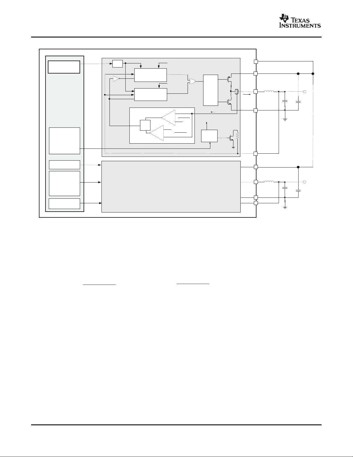
www.ti.com
GATE
CONTROL
LOGIC
SM1 OUTPUT
VOLTAGESETTING
SM1/SM2 PHASE
CONTROL
I2C
REGISTERS
SM1 OPERATING
MODE:
ON/OFF,
PWM, PFM, S TANDBY
SM1 DISCHARGE
SWITCHENABLE ,
LOWPFMRIPPLE
L1
PGND1
VIN_SM1
SM1
SM2 OUTPUT
VOLTAGESETTING
L2
PGND2
VIN_SM2
SM2
SM 1 CONVERTER
3.3 Hµ
10 Fµ
V
O(SM1)
10 Fµ
3.3 Hµ
10 Fµ
V
O(SM2)
10 Fµ
OUT
P1
P2
+
_
+
_
29 Ω
V( VIN _S M1)
39 Ω
V(VIN_SM1)
SET
RESET
OUT
EN_PFM
POWERSTAGE
CURRENT COMPARATORS
I(L1)
I(L1)
SM1
CONTROL
LOGIC
EN_PFM
EN_PWM
EN_ALL
DCHGON
SM2 OPERATING
MODE:
ON/OFF,
SM1 DISCHARGE
SWITCHENABLE ,
LOWPFMRIPPLE
TPS65810
LSM1
LSM2
C21
C22
C19
C20
PWMCONTROL
PFMCONTROL
PFMON
PWMON
DAC
EN_PWM
SM2CONVERTER
SAMETOPOLOGY ASSM1CONVERTER
PWM, PFM, S TANDBY
PWM, PFM, S TANDBY
I
PFM(LEAVE)
+
V(VIN_SM3)
29 W
,
I
PFM(ENTER)
+
V(VIN_SM3)
39 W
TPS65810
TPS65811
SLVS658B – MARCH 2006 – REVISED FEBRUARY 2007
Figure 41. SM1/SM2 Converter
The TPS65810 SM1 and SM2 buck converters can be set to operate only in PWM mode or to switch
automatically between PFM and PWM modes. The average load current is monitored, and the PFM mode is set
if the average load current is below the threshold IPFM(ENTER). When in PFM mode the load current is also
monitored, and the PWM mode is set when the load current exceeds the threshold I
PFM(LEAVE)
. The thresholds for
automatic PFM/PWM switching are calculated as shown in Equation 6 for the SM1 converter, the same
thresholds apply to the SM2 converter by replacing VIN_SM1 by VIN_SM2:
The automatic switching mode is enabled via the control bits PFM_SM1 and PFM_SM2 on I2C registers
SM1_SET1 and SM2_SET1.
Output Voltage Slew Rate
I2C registers enable setting the output voltage slew rate, when transitioning from one programmed voltage to a
new programmed voltage value. These events can be triggered by a new output voltage selection or by switching
from a low power mode (standby) to a normal operating mode. During a transition, the output voltage is stepped
from the currently programmed voltage to the new target voltage. The slew rate from the initial voltage to the final
voltage can be selected using I2C registers, SM1_SET2 and SM2_SET2, ranging from 0.24 mv/ µ s to 15.36
mV/ µ s for the SM1 converter and 0.48 to 30.72 mV/ µ S for the SM2 converter. If the slew rate is set to OFF the
output voltage goes from the current value to the programmed value in a single step.
During the transition to standby mode the Power Good comparators are disabled.
(6)
60 Submit Documentation Feedback Copyright © 2006 – 2007, Texas Instruments Incorporated
Product Folder Link(s): TPS65810 TPS65811

www.ti.com
V(VIN_SM1) v V(SM1) ) I(L1)ǒR
DSON(PSM1)
) R
L
Ǔ
TPS65810
TPS65811
SLVS658B – MARCH 2006 – REVISED FEBRUARY 2007
Soft Start
SM1 and SM2 have an internal soft start circuit that limits the inrush current during start-up. An initial delay (170
µ sec typ) from the converter enabled command to the converter effectively being operational is required, to
assure that the internal circuits of the converter are properly biased. At the end of that initial delay the soft start is
initiated, and the internal compensation capacitor is charged with a low value current source. The soft start time
is typically 750 µ s, with the output voltage ramping from 5% to 95% of the final target value.
Dropout Operation at 100% Duty Cycle
The TPS65810 buck converters offer a low input to output voltage difference while still maintaining operation
when the duty cycle is set to 100%. In this mode of operation the P-channel switch is constantly turned on,
enabling operation with a low input voltage. The dropout operation starts if:
Where:
I(L1) = Output current plus inductor ripple current.
R
= DC resistance of the inductor
L
Equation 7 can be also used for the SM2 converter, replacing SM1 by SM2 and L1 by L2.
Output Voltage Monitoring
The output voltage of converters SM1 and SM2 is monitored by internal comparators, and an output low voltage
condition is detected when the output voltage is below 90% of the programmed value. The power good status for
SM1 and SM2 is accessible via I2C, see interrupt controller section for more details.
The power good comparators for SM1 and SM2 are disabled during the transition to standby mode operation.
They are enabled when the transition to standby mode is complete.
(7)
Standby Mode
Using the I2C SM1 and SM2 can be set in stand-by mode. In STANDBY mode the PFM operation mode is set
and the output voltage is defined by I2C registers SM1_STANDBYand SM2_STANDBY, and it can be set to a
value different than the normal mode output regulation voltage. The standby mode can also be set by the GPIO
pins, if those are configured as control pins that define the SM1/SM2 operating mode.
PWM Operation
During PWM operation the converters use a fast response voltage mode controller scheme with input voltage
feed-forward, enabling the use of small ceramic input and output capacitors. At the beginning of each clock cycle
the P-channel MOSFET switch is turned on, and the oscillator starts the voltage ramp. The inductor current
ramps up until the ramp voltage reaches the error amplifier output voltage, when the comparator trips and the
p-channel MOSFET switch is turned off. Internal adaptative break-before-make circuits turn on the integrated
n-channel MOSFET switch after an internal, fixed dead-time delay, and the inductor current ramps down, until
the next cycle is started. When the next cycle starts the ramp voltage is reset to its low value and the p-channel
MOSFET switch is turned on again.
Copyright © 2006 – 2007, Texas Instruments Incorporated Submit Documentation Feedback 61
Product Folder Link(s): TPS65810 TPS65811

www.ti.com
GATE
CONTROL
LOGIC
OSC
PGND1
VIN_SM1
3.3 Hm
OUT
(L1)
+
_
+
_
LSM1
OUTPUT
VOLTAGE
SETTING
PWMCONTROL SECTION
(SHOWNFORSM1,SAMETOPOLOGY FORSM2)
RAMP PEAK-TO-PEAKVOLTAGE
PROPORTIONAL TOVIN_SM1
ERROR AMP WITH “TYPE-3
LIKE” COMPENSATION
V
O(SM1)
C21
10 Fm
C22
10 Fm
L1
SM1
TPS65810
TPS65811
SLVS658B – MARCH 2006 – REVISED FEBRUARY 2007
Figure 42. PWM Operation
The integrated power MOSFETs current is monitored at all times and the power MOSFET is turned off if its
internal short circuit current limit is reached.
Phase Control in PWM Mode
The SM1 and SM2 converters operate synchronized to each other when both are in PWM mode, with converter
SM1 as the master. I2C control register bits S1S2PHASE in register SM1_SET2 enables delaying the SM2 PWM
clock with respect to SM1 PWM clock, selecting a phase shift from 0 to 270 degrees. The out-of-phase operation
reduces the average current at the input node, enabling use of smaller input filter capacitors when both
converters are connected to the same input supply.
PFM Mode Operation
Using the I2C interface the SM1 and SM2 converters can have the automatic power saving PFM mode enabled.
When the PFM mode is set the switching frequency is reduced and the internal bias currents are decreased,
optimizing the converter efficiency under light load conditions.
In PFM mode, the output voltage is monitored by a voltage comparator, which regulates the output voltage to the
programmed value, V
. If the output voltage is below V
O(SM1)
, the PFM control circuit turns on the power
O(SM1)
stage, applying a burst of pulses to increase the output voltage. When the output voltage exceeds the target
regulation voltage, V
, the power stage is disabled, and the output voltage drops until it is below the
O(SM1)
regulation voltage target, when the power stage is enabled again.
62 Submit Documentation Feedback Copyright © 2006 – 2007, Texas Instruments Incorporated
Product Folder Link(s): TPS65810 TPS65811

www.ti.com
GATE
CONTROL
LOGIC
L
1
PGND1
VIN_SM1
SM1
OUT
P1
-
_
+
_
+
_
SET
RESET
OUT
OUTPUT VOLTAGE
COMPARATOR
POWERSTAGEPEAK
CURRENT COMPARATORS
I(L1)
I(L1)
LSM1
BIASCONTROL
PFMCONTROL SECTION
(SHOWNFORSM1,SAMETOPOLOGY FORSM2)
V(VIN_SM1)
39 W
V(VIN_SM1)
29 W
V
O(SM1)
+
3.3 Hm
V
O(SM1)
C21
10 Fm
C22
10 Fm
BURST
V
(OUT)
I
PFM(ENTER)
I
PFM(LEAVE)
BURST
INDUCTOR
CURRENT
OUTPUT
VOLTAGE
LOWRIPPLE
PFMOPERATION
MAXIMUMEFFICIENCY
PFMOPERATION
T
COMP
T
COMP
T
COMP
T
COMP
TPS65810
TPS65811
SLVS658B – MARCH 2006 – REVISED FEBRUARY 2007
Figure 43. PFM Mode Operation
During burst operation two current comparators control the power stage integrated MOSFETs. These
comparators monitor the instantaneous inductor current and compare it to the internal thresholds I
I
PFM(LEAVE)
inductor current exceeds I
, turning the p-channel switch on if the inductor current is less than I
PFM(ENTER)
. The n-channel switch is turned on when the p-channel MOSFET is off.
PFM(LEAVE)
and turning it off if the
The PFM output voltage comparator quiescent current may be reduced using the I2C register bits PFM_RPL1
and PFM_RPL2 in registers SM1_SET and SM2_SET. The voltage comparator quiescent current is reduced if
PFM_RPL1 and PFM_RPL2 bits are set to LO, and the comparator response time (t
COMP
increases. A reduction in quiescent current increases the converter efficiency at light loads, at the expense of a
larger output voltage ripple when in PFM mode.
The ripple is minimized if PFM_RPL1 and PFM_RPL2 bits are set to HI, at the expense of reduced efficiency
under light loads. The operation under low and high ripple settings is described in Figure 44 .
PFM(ENTER)
, see Figure 44 )
and
When a burst of pulses is generated, the PFM current comparators control the power-stage MOSFETs to limit
the inductor current to a value between the thresholds I
burst cycle is proportional to the load current, and the average current is always below I
operation is set. The typical burst operation in PFM mode is shown in Figure 45 .
Copyright © 2006 – 2007, Texas Instruments Incorporated Submit Documentation Feedback 63
Figure 44. PFM mode operation waveforms
Product Folder Link(s): TPS65810 TPS65811
and I
PFM(ENTER)
PFM(LEAVE)
. The number of pulses in a
PFM(LEAVE)
once PFM

www.ti.com
BURST
I
PFM(LEAVE)
LOADCURRENT
V(OUT)
I
PFM(LEAVE)
I
PFM(ENTER)
INDUCTORCURRENT
TPS65810
TPS65811
SLVS658B – MARCH 2006 – REVISED FEBRUARY 2007
Figure 45. Typical Burst Operation in PFM Mode
The PFM operation is disabled and PWM operation set if one of the following events happen during PFM
operation:
1. The total burst operation time exceeds 10 µ s, typ.
2. The output voltage falls below 2% of the target regulation voltage.
The PFM mode can be disabled through the serial interface to force the individual converters to stay in fixed
frequency PWM mode.
64 Submit Documentation Feedback Copyright © 2006 – 2007, Texas Instruments Incorporated
Product Folder Link(s): TPS65810 TPS65811

www.ti.com
TPS65810
TPS65811
SLVS658B – MARCH 2006 – REVISED FEBRUARY 2007
SWITCHED-MODE STEP-DOWN CONVERTERS — I2C REGISTERS
The I2C registers that control buck converter-related functions are shown below. The HEX address for each
register is shown by the register name, together with the R or W functionality for the register bits. Shaded values
indicate default initial power-up values.
B7 B6 B5 B4 B3 B2 B1 B0
SM1_SET1, ADDRESS=10, ALL BITS R/W
Bit name SM1 EN PFM_RPL1 PFM_SM1 SetV4_SM1 SetV3_SM1 SetV2_SM1 SetV1_SM1 SetV0_SM1
Function SM1 ON/OFF SM1 PFM SM1 PFM SM1 OUTPUT VOLTAGE REGULATION VALUE, STANDBY MODE NOT SET
When 0 OFF MAXIMIZE PWM/PFM See Table 9 for SM1, SM2 voltage setting, Power up default=1.24 V
When 1 ON MINIMIZE Only PWM
SM1_SET2, ADDRESS=11, ALL BITS R/W
Bit name NOT USED STANDBY_SM DISCHSM1 S1S2PHASE_1 S1S2PHASE_0 SLEWSM1_2 SLEWSM1_1 SLEWSM1_0
Function NOT USED SM1 STANDBY SM1 output SM2 PWM CLOCK DELAY, SM1 OUTPUT SLEW RATE SETTING
When 0 NOT USED OFF OFF 00 = 0 ° 10 = 180 ° 000 = 0.24 010 = 0.96 100 = 5.84 110 = 15.36
When 1 NOT USED ON ON
SM1_STANDBY, ADDRESS=12, B4-B0 R/W, B7-B5 READ ONLY
Bit name GPIO3LVL GPIO2LVL GPIO1LVL SetV4_SM1SL SetV3_SM1SL SetV2_SM1SL SetV1_SM1SL SetV0_SM1SL
Function GPIO3 pin logic GPIO2 pin logic GPIO1 pin logic SM1 OUTPUT VOLTAGE REGULATION VALUE, STANDBY MODE SET
When 0 LO LO LO See Table 9 for SM1, SM2 voltage setting, Power-up default = 1.24 V
When 1 HI HI HI
SM2_SET1, ADDRESS=13, ALL REGISTER BITS R/W
Bit name SM2 EN PFM_RPL2 PFM_SM2 SetV4_SM2 SetV3_SM2 SetV2_SM2 SetV1_SM2 SetV0_SM2
Function SM2 ON/OFF SM2 PFM SM2 PFM SM2 OUTPUT VOLTAGE REGULATION VALUE, STANDBY MODE NOT SET
When 0 OFF MAXIMIZE PWM/PFM See Table 9 for SM1, SM2 voltage setting, Power-up default = 3.32 V
When 1 ON MINIMIZE ONLY PWM
SM2_SET2, ADDRESS=14, ALL REGISTER BITS R/W
Bit name NOT USED STANDBY_SM DISCHSM2 NOT USED NOT USED SLEWSM2_2 SLEWSM2_1 SLEWSM2_0
Function NOT USED SM2 STANDBY SM2 output NOT USED NOT USED SM2 OUTPUT SLEW RATE SETTING
When 0 NOT USED OFF OFF NOT USED NOT USED 000 = 0.48 010 = 1.92 100 = 7.68
When 1 NOT USED ON ON NOT USED NOT USED
SM2_STANDBY, ADDRESS=15, ALL REGISTER BITS R/W
Bit name NOT USED NOT USED NOT USED SetV4_SM2SL SetV3_SM2SL SetV2_SM2SL SetV1_SM2SL SetV0_SM2SL
Function NOT USED NOT USED NOT USED SM1 OUTPUT VOLTAGE REGULATION VALUE, STANDBY MODE SET
When 0 NOT USED NOT USED NOT USED See Table 9 for SM1, SM2 voltage setting, Power up default=3.32 V
When 1 NOT USED NOT USED NOT USED
CONTROL FUNCTION MODE ON/OFF
OPERATION CTRL
EFFICIENCY
OUTPUT
RIPPLE
1
MODE ON discharge WITH RESPECT TO SM1 PWM
switch enable CLOCK
01 = 90 ° 11 = 270 ° 001 = 0.48 011 = 1.92 101 = 7.68 111 =
Default = 180 ° IMMEDIATE
Unit: mV/ µ s Default= 15.36
level level level
CONTROL FUNCTION MODE ON/OFF
OPERATION CTRL
EFFICIENCY
OUTPUT
RIPPLE
2
MODE ON discharge
switch enable
110 = 30.72 001 = 0.096 011 = 3.84
101 = 15.36 111 = IMMEDIATE
Unit: mV/ µ s Default = 30.72
Copyright © 2006 – 2007, Texas Instruments Incorporated Submit Documentation Feedback 65
Product Folder Link(s): TPS65810 TPS65811

www.ti.com
TPS65810
TPS65811
SLVS658B – MARCH 2006 – REVISED FEBRUARY 2007
Table 9. Programmable Settings for SM1 and SM2 (Including STANDBY)
SetV4_ SetV3_ SetV2_ SetV1_ SetV0_ Vset SM1 Vset SM2 SetV4_ SetV3_ SetV2_ SetV1_ SetV0_ Vset SM1 Vset SM2
SM SM SM SM SM SM SM SM SM SM
0 0 0 0 0 0.6 1 1 0 0 0 0 1.24 2.28
0 0 0 0 1 0.64 1.08 1 0 0 0 1 1.28 2.36
0 0 0 1 0 0.68 1.16 1 0 0 1 0 1.32 2.44
0 0 0 1 1 0.72 1.24 1 0 0 1 1 1.36 2.52
0 0 1 0 0 0.76 1.32 1 0 1 0 0 1.4 2.6
0 0 1 0 1 0.8 1.4 1 0 1 0 1 1.44 2.68
0 0 1 1 0 0.84 1.48 1 0 1 1 0 1.48 2.76
0 0 1 1 1 0.88 1.56 1 0 1 1 1 1.52 2.84
0 1 0 0 0 0.92 1.64 1 1 0 0 0 1.56 2.92
0 1 0 0 1 0.96 1.72 1 1 0 0 1 1.6 3
0 1 0 1 0 1 1.8 1 1 0 1 0 1.64 3.08
0 1 0 1 1 1.04 1.88 1 1 0 1 1 1.68 3.16
0 1 1 0 0 1.08 1.96 1 1 1 0 0 1.72 3.24
0 1 1 0 1 1.12 2.04 1 1 1 0 1 1.76 3.32
0 1 1 1 0 1.16 2.12 1 1 1 1 0 1.8 3.4
0 1 1 1 1 1.2 2.2 1 1 1 1 1 0.6 1
A
SM1, SM2 PHASE SMX_SLEW RATE, SMX = SM1 OR SM2
S1S2_PHASE1 S1S2_PHASE0 PHASE SLEWX_2 SLEWX_1 SLEWX_0
0 0 0 ° 0 0 0 0.24 0.48
0 1 90 ° 0 0 1 0.48 0.96
1 0 180 ° 0 1 0 0.96 1.92
1 1 270 ° 0 1 1 1.92 3.84
1 0 0 3.84 7.68
1 0 1 7.68 15.36
1 1 0 15.36 30.72
1 1 1 Immediate
SM1 SM2
mV/ µ s mV/ µ s
66 Submit Documentation Feedback Copyright © 2006 – 2007, Texas Instruments Incorporated
Product Folder Link(s): TPS65810 TPS65811

www.ti.com
ANLG1
ANLG2
ADC _REF
8 CHANNEL
MUX
A/D
CONVERTER
ADC
AGND 2
OUT
A 2
A 2
SYSTEMPOWERBUS
ADC
CONTROL
LOGIC
EXTERNAL ANALOG
INPUTVOLTAGE
6INTERNAL
CHANNELS
C17
4.7 Fm
SLVS658B – MARCH 2006 – REVISED FEBRUARY 2007
FUNCTIONALITY GUIDE – ANALOG TO DIGITAL CONVERTER
10 BIT SUCCESSIVE APPROXIMATION ADC
ADC Input Channels Trigger Mode Conversion Converter Mode Trigger Delay Wait Time, Multiple Power Up
Internal External Range Min Step
Charge ANLG1 and 1, 4, 8, 16, 32, Single, Average, 0-750 µ s, 50 µ s µ s: 20, 40, 60, 80, 160, ADC off
Current, ANLG2 64, 128, 256 Find max value, 16 steps 240, 320, 640
Thermistor voltages Find min value
temperature,
IC junction
temperature,
RTC_OUT
voltage, OUT
voltage,
Battery
voltage
Fixed Selectable via Selectable via Selectable via Selectable via Selectable Selectable
internally
I2C I2C I2C I2C via I2C via I2C
GPIB, I2C
driven, Repeat
Count Conversions Default
ms: 1.28, 1.92, 2.56,
5.12, 10.24, 15.36, 20.48
Selectable via I2C
TPS65810
TPS65811
Figure 46. Required External Components, Recommended Values, External Connections
ANALOG-TO-DIGITAL CONVERTER
Overview
The TPS65810 has a 10 bit integrated successive approximation A/D, capable of running A/D conversions on
eight distinct channels in a variety of modes. Two of the eight channels are connected to uncommitted pins
ANLG1 and ANLG2, and can be used to convert external voltages. The other six channels monitor system
parameters which are critical to the overall system monitoring. The channel selection is set via I2C.
A dedicated set of I2C registers enables configuration of the ADC to perform a conversion cycle with either a
single conversion or a multiple conversions. The ALU generates a data set containing maximum value detection,
minimum value detection and average value calculation for each conversion cycle. Each cycle can be performed
a single time or multiple times.
Input Channels
The following channels are available for selection via the I2C register ADC_SET bits CHSEL_SET bits:
Copyright © 2006 – 2007, Texas Instruments Incorporated Submit Documentation Feedback 67
Product Folder Link(s): TPS65810 TPS65811

www.ti.com
TPS65810
TPS65811
SLVS658B – MARCH 2006 – REVISED FEBRUARY 2007
Table 10. ADC input channel overview
Channel Connection Parameter Sampled Voltage Range Under Special Features Full Scale Reading LSB
CH1 ANLG1 pin User defined User defined Internal pullup current 2.535 V Full scale
CH2 ANLG2 pin 2.535 V
CH3 ISET1 pin Voltage proportional to 0 V (charger off) to — 2.535 V
charge current 2.525 V (fast charge)
CH4 TS pin Voltage proportional to pack 0 V (short) to 4.7V (no No internal pullup 2.535 V
temperature thermistor) current, use external
CH5 Internal Voltage proportional to IC 1.85 V at TJ= 25 ° C, — 2.535 V
junction junction temperature – 6.5 mV/ ° C slope typ
temperature
CH6 RTC_OUT Internal LDO output voltage 0 V to 3.3 V — 4.7 V
pin
CH7 OUT pin System Power bus voltage 0 V to 4.4 V — 4.7 V
CH8 BAT pin Battery pack positive 0 V to 4.4 V — 4.7 V
terminal voltage
FUNCTIONAL OVERVIEW
The TPS65810 ADC can be subdivided in four sections:
1. Input selection: The input selection section has two major blocks, the input bias control and an 8 channel
MUX. The input bias control provides the bias currents that are applied to pins ANLG1 and ANLG2. The bias
currents for pins ANLG1 and ANLG2 are set on I2C register ADC_WAIT.
The ANLG1 pin current source is automatically enabled when the input power is detected, providing the
required setup to measure a battery ID resistor (ANLG1 pin). ANLG1 and ANLG2 can be used to measure
external resistive loads or analog voltages. The bias current sources are always connected to the OUT pin
internally.
The internal MUX connects one of the monitored analog inputs to the ADC engine, following the selection
defined on register ADC_SET.
2. ADC engine: The ADC engine uses an internal or external voltage reference, as defined by the ADC_REF
bit on the ADC_SET control register. If the internal reference is selected ADC_REF is connected to an
internal LDO that regulates the ADC_REF pin voltage to generate the ADC supply and internal voltage
reference. The internal LDO maximum output current is 6 mA typical, and a conversion should be started
only after the external capacitor is fully charged.
If an external reference is used it should be connected to the ADC_REF pin. When an external reference is
selected the internal LDO connected to ADC_REF is disabled. Care must be taken when selecting an
external reference as the ADC reference voltage, as it affects the ADC LSB absolute value.
3. Trigger control and synchronization: The ADC engine starts a conversion of the selected input when the
trigger control circuit sends a start command. The trigger control circuit starts the ADC conversion and
transfers the ADC output data to the arithmetic logic unit (ALU) at the end of the conversion. It also
synchronizes the data transfer from the ALU to the I2C ADC_READING register at the end of a conversion
cycle, and generates the ADC status information sent to the ADC registers.
An ADC engine conversion is triggered by the TPS65810 trigger control circuit using either an internal trigger
or an external trigger. The internal trigger is automatically generated by the TPS65810 at the end of each
ADC engine conversion, following the timing parameters set on I2C registers ADC_SET, ADC_DELAY and
ADC_WAIT.
The GPIO3 pin can be used as an external trigger if the bit ADC_TRG_GPIO3 is set HI, in the I2C register
ADC_DELAY. In the external trigger mode a new conversion is started after the GPIO3 pin has an edge
transition, following the timing parameters set on I2C registers ADC_SET, ADC_DELAY and ADC_WAIT.
Normal Operating (Internal reference value
Conditions selected )
source programmable reading
via I2C: 0/ 10/50/60 µ A ÷ 1023
pullup resistor to bias
pack thermistor
68 Submit Documentation Feedback Copyright © 2006 – 2007, Texas Instruments Incorporated
Product Folder Link(s): TPS65810 TPS65811

www.ti.com
8 CHANNEL
MUX
CURRENT SAMPLE
ARITHMETICLOGIC
UNIT
ANLG1
ANLG2
T
J
TS
ISET1
RTC_OUT
OUT
BAT
10 BIT SUCCESSIVE
APROXIMATION ADC
SUPPLY REF
ACCUMULATOR
TRIGGERCONTROL
AND
SYNCHRONIZATION
START DONE
ADCREFERENCE
ANDSUPPLY
SELECTION
BIASCONTROL
ANLG 1/
ANLG 2 BIAS
SELECTION
ADCSUPPLY
AND
REFERENCE
SELECTION
OUT
ADC
CHANNEL
SELECTION
ADCCONFIGURATION :
TRIGGER, HOLDOFF, REPEAT
MODES
DELAY ANDWAIT TIMING
ALUMODE :
SINGLE,
AVERAGE ,
MIN,, MAX
TOI2C:
STATUS AND
CONVERSION
DATA
ADC_REF
I2C
I2C
TPS65810
A 2
4.7 Fm
TPS65810
TPS65811
SLVS658B – MARCH 2006 – REVISED FEBRUARY 2007
4. Arithmetic Logic Unit (ALU): The ALU performs mathematical operations on the ADC output data as
defined by the I2C ADC_READING registers. It executes average calculations or minimum /maximum
detection. The result of the calculations is stored in a 11 bit accumulator register (1 bit allocated for
carry-over). The accumulator value is transferred to the I2C data register at the end of a conversion cycle.
A simplified block diagram for the ADC is shown in Figure 47 .
Figure 47. ADC Simplified Block Diagram
ADC Conversion Cycle
A conversion cycle includes all the steps required to successfully sample the selected input signal and transfer
the converted data to the I2C, generating an interrupt request to the host ( pin: HI → LO). The number of individual
conversions (samples) in a conversion cycle is defined by the I2C ADC_SET register bits READ_MODE settings,
and can range from a single sample to 256 samples. The conversion cycle settings for the ALU is defined by
register ADC_READING and it can be set to average, maximum value detection, minimum value detection or no
processing (ADC engine output loaded in the accumulator directly).
The conversion cycle starts with the first sampling and ends when:
• The required ALU operations are performed on the final sample, and
• The ALU accumulator data is transferred to the I2C ADC_READING register, and
• The register bit ADC_STATUS in the ADC_READING register is set to LO.
A conversion cycle is always started by the external host when the ADC_EN bit in the ADC_SET register is
toggled from LO to HI by a I2C write operation. Resetting the ADC_EN bit to LO before the current conversion
cycle ends ( INT: LO → HI, ADC_STATUS bit set to LO) is not recommended, as the ADC keeps its current
configuration until the current conversion cycle ends.
At the end of a conversion cycle the output data is stored at registers in the ALU block. The ADC_STATUS bit is
set to LO ( DONE ) and an interrupt is generated ( INT pin: HI → LO ) if the ADC_STATUS bit is unmasked, at the
interrupt masking registers INT_MASK. It should be noted that the minimum, maximum and average values are
ALWAYS calculated by the ALU for each conversion cycle.
Copyright © 2006 – 2007, Texas Instruments Incorporated Submit Documentation Feedback 69
Product Folder Link(s): TPS65810 TPS65811

www.ti.com
GPIO3
INTERNAL ADC
CONVERSIONSTART
CONVERTER
MODE
ARMED
CONVERTING
T
DLY(TRG)
T
DLY(TRG)
TPS65810
TPS65811
SLVS658B – MARCH 2006 – REVISED FEBRUARY 2007
The value loaded in the I2C registers ADC READING_HI and ADC READING_LO at the end of a conversion
cycle is defined by control bits ADC_READ0 and ADC_READ1 in register ADC READING_HI. The average,
minimum, maximum, and last-sample values for a conversion cycle can be read if the external host executes an
I2C write operation, changing the values of bits ADC_READ0 and ADC_READ1, followed by an I2C read
operation on registers ADC READING_HI and ADC READING_LO. The minimum, maximum, average, and last
values have the same value if a conversion cycle with only one sample is executed.
The ADC_READ0 and ADC_READ1 bits can not be modified during the execution of a conversion cycle. A new
conversion cycle should be started only after the current conversion cycle is completed, by toggling the ADC_EN
bit from HI to LO and HI again.
External Trigger Operation
The trigger control circuit can be programmed to use an external signal to start a conversion. The TPS65810
GPIO3 input is configurable as an ADC trigger, with ADC conversion starting on either a rising edge or falling
edge. When using an external trigger the trigger delay, trigger wait time delay and trigger hold-off mode can be
programmed using I2C registers.
The procedure to start an externally-triggered conversion cycle has the following steps:
1. Verify that the current conversion cycle has ended (ADC_STATUS=LO, I2C register ADC_READING_HI)
2. Set ADC_EN=LO
3. Configure ADC sampling mode, ALU mode, trigger parameters, etc.
4. Set ADC_EN=HI
After step 4 the ADC is armed, waiting for an external trigger detection to start a conversion cycle. Similarly to
the non-triggered mode, the ADC configuration should not be modified until the current conversion cycle ends.
Note that in the external trigger mode the current cycle does not end if the converter is armed and an external
trigger is not detected.
Detecting an External Trigger Event
An external trigger event is detected when the GPIO3 input has an edge that matches the edge detection
programmed in the EDGE bit, at the I2C register ADC_DELAY. The internal ADC trigger can be delayed with
respect to the external trigger signal edge. The delay time value is set by the ADC_DELAY register bits
DELAY_n, and can range from 0 µ s (no delay) to 750 µ sec. A conversion is started only if the external trigger
remains at its active level when the delay time expires, as shown in Figure 48 . In a positive-edge detection the
active trigger level is HI; in a negative-edge detection the active trigger level is LO.
Figure 48. ADC Conversion Triggered by GPIO3 Positive Edge Triggered Active Level Hi
Executing Multiple-Sample Cycles With an External Trigger
When executing conversion cycles that require multiple samples it may be desirable to synchronize the input
signal conversion using either an external trigger that has a periodic repetition rate or an external asynchronous
trigger that indicates when the external input signal being converted is valid. The TPS65810 has additional
operating modes and timing parameters that can be programmed using the I2C to configure multiple sample
conversion cycles.
In multiple sample cycles the host can select the wait time between samples using the bits WAITn in the
ADC_WAIT register to set the wait time between samples. The wait time is measured between the end of a
conversion and the start of a new conversion.
70 Submit Documentation Feedback Copyright © 2006 – 2007, Texas Instruments Incorporated
Product Folder Link(s): TPS65810 TPS65811
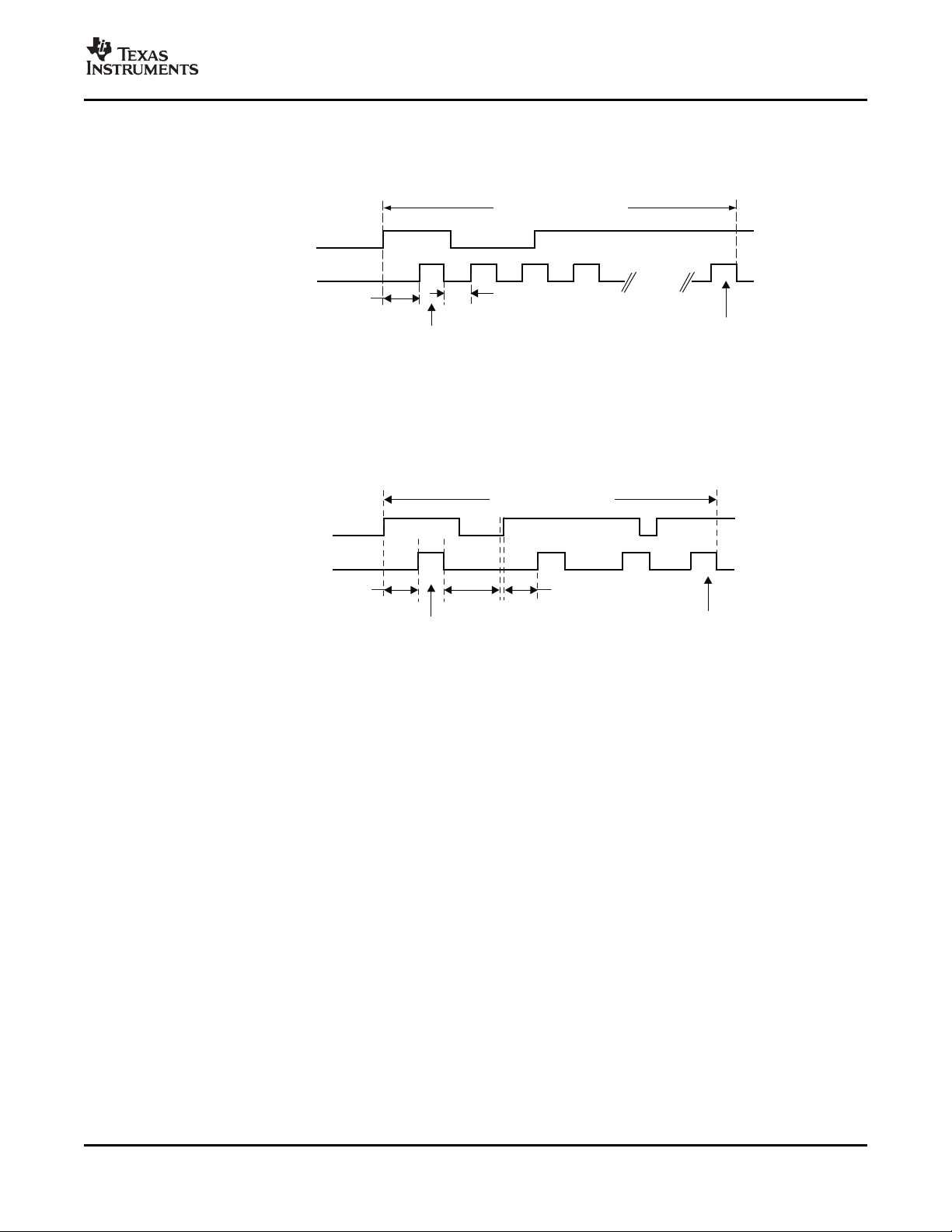
www.ti.com
GPIO3
INTERNAL ADC
CONVERSIONSTATUS
FIRST
SAMPLE
LAST
SAMPLE
ON
OFF
t
WAIT(TRG)
t
DLY(TRG
)
CONVERSIONCYCLE
GPIO3
INTERNAL ADC
CONVERSIONSTATUS
FIRST
SAMPLE
LAST
SAMPLE
ON
OFF
T
WAIT(TRG)
T
DLY(TRG)
T
DLY(TRG)
CONVERSIONCYCLE
TPS65810
TPS65811
SLVS658B – MARCH 2006 – REVISED FEBRUARY 2007
With the default power-up settings (HOLDOFF=LO, ADC_DELAY register), the TPS65810 executes a
multiple-sample conversion cycle if the first sample is taken when the trigger is at its active level. Subsequent
samples are converted at the end of the wait time, even if the trigger returns to the non-active level. The external
trigger level edge is ignored until the current conversion cycle ends.
Figure 49. ADC Conversion Triggered by GPIO3 Positive Edge Triggered Active Level Hi, Holdoff = LC
If the sample conversion needs to be synchronized with an external trigger, during multiple sample conversion
cycles, the control bit HOLDOFF should be set to HI. When the holdoff mode is active, the internal trigger starts
a sample conversion only if the external trigger was detected and is at its active level at the end of the wait time,
as shown in Figure 50 .
When the multiple sample cycles are executed the host must configure the maximum and minimum limits for the
ADC output using registers DLOLIM1, DLOLIM2, DHILIM1 and DHILIM2. A conversion cycle ends if any
individual conversion result exceeds the maximum limit value or is below the minimum limit value. When an out
of limit conversion is detected an interrupt is sent to the host, and the ADC_STATUS bit on register ADC
READING_HI is set to DONE.
Continuous Conversion Operation (Repeat Mode)
The TPS65810 ADC can be set to operate in a continuous conversion mode, with back-to-back conversion
cycles executed. The REPEAT mode is targeted at applications where an input is continuously monitored for a
period of time, and the host must be informed if the monitored input is out of the range set by I2C registers
DLOLIM1, DLOLIM2, DHILIM1 and DHILIM2. In REPEAT mode each conversion is started when the ADC trigger
(internal or external) is detected, and a new conversion cycle is started when the current conversion cycle ends.
All the trigger and sampling modes available for normal conversion cycles are available in repeat mode.
Executing I2C read operations to get the ADC readings for average, minimum, maximum and last sample values
is possible in REPEAT mode. However, this is not a recommended operation, as the REPEAT mode does not
generate a DONE status flag making it difficult to synchronize the ADC data reading to the end of a conversion
cycle.
The recommended use of the REPEAT mode is:
1. Configure the ADC conversion cycle: trigger mode, sample mode, select input signal, etc.
2. Configure the HI and LO limits for the ADC readings
3. Set the ADC_DELAY register bit REPEAT to HI
4. Toggle ADC_DELAY register bit ADC_EN bit from LO to HI
Copyright © 2006 – 2007, Texas Instruments Incorporated Submit Documentation Feedback 71
Figure 50. ADC Conversion Triggered by GPIO3 Positive Edge Triggered Active Level HI,
Holdoff = HI, Four Sample Cycles
Product Folder Link(s): TPS65810 TPS65811

www.ti.com
TPS65810
TPS65811
SLVS658B – MARCH 2006 – REVISED FEBRUARY 2007
5. Monitor the INT pin. An interrupt triggered by ADC_STATUS=LO indicates that the selected input signal is
out of range
To exit the continuous mode the host must follow the steps below, if external trigger mode was set:
1. Exit external trigger mode
2. Set REPEAT bit to LO, effectively terminating the repeat mode. This generates an additional conversion; at
the end of this conversion the ADC is ready for a new configuration.
3. Set ADC_EN to LO after on-going conversion ends.
To exit the continuous mode the host must follow the steps below, if internal trigger mode was set:
1. Set REPEAT bit to LO, effectively terminating the repeat mode.
2. Set ADC_EN to LO, after on-going conversion ends
ADC Input Signal Range Setting
The registers DHILIMn and DLOLIMn can be used by the host to set maximum and minimum limits for the DAC
engine output. At the end of each conversion the ADC output is checked for the maximum and minimum limits,
and a status flag is set if the converted data exceeds the high limit or is under the low limit. In multiple sample
operation the converted data range is checked when all programmed samples have been converted.
The host can mask or unmask interrupts caused by the ADC range status bits using the INT_MASKn registers.
72 Submit Documentation Feedback Copyright © 2006 – 2007, Texas Instruments Incorporated
Product Folder Link(s): TPS65810 TPS65811

www.ti.com
LOAD ADC
CONFIGURATION
DATA FROMI2C
TRIGGERMODE,
TRIGGERDELAY
SAMPLEWAIT TIME,
HOLDOFFMODE
REPEAT ON/OFF
ALUMODE : AVG/MAX/MIN
NUMBEROFSAMPLES
ADCINPUT RANGE
ADCCHANNEL
ADC
ENABLED
(I2C) ?
TRIGGER
EDGE
DETECT
EXTERNAL
TRIGGER
HOLDOFF
ON
1) SET ADC
BUSY STATUS
2) START
CONVERSION
TRIGGER
EDGE
MODE
TRIGGER
HI
TRIGGER
LO
N
CONVERSIONS
?
N
TH
CONVERSION
DONE
WAIT TIME
0 µsto 20.5 msec
STARTTRIGGER
DELAY
1) LOADDATA IN
ALU
2) ALUOUTPUT
STOREDIN
ACCUMULATOR
ALU
DATAOUT OF
RANGE
REPEAT
MODE
1
) LOADI2CDATA
REGISTERWITH
ALUDATA
2) SET ADCSTATUS
TODONE
3) INT SENT TOHOST
IFNON-MASKED
1) SET ADC_HIOR
ADC_ LOFAULT
2) SET ADCSTATUS
TODONE
3) INT SENT TOHOST
IFNON-MASKED
CURRENT
CYCLEENDS
HOSTSTARTSNEW
CONVERSION
CYCLEBY SETTING
ADC_EN=HI
YES
NO
YES
YES
YES,CHECK
TRIGGER
NO
NO
NO
NO
NO
NO,SEND
DATA
TOI2C
YESFAULT
DETECTED
YES
NO
FALLING
EDGE
RISING
EDGE
ADCCONVERSION
COMPLETE
ALUOUTPUT
DATAREADY
YES
TRIGGER
VALID
TRIGGER
DELAY
OVER
NO,OPPOSITE
TRIGGEREDGE
HAPPENED
BEFOREDELAY
TIME
NO
YES
ADC
ENABLED
(I2C) ?
NO
YES
NO,SEND
DATA
TOI2C
ADC
ENABLED
(I2C) ?
NO, HOSTENDS
CURRENT
CONVERSION
CYCLESETTING
ADC_EN=LO
YES,CURRENT
CONVERSION
CYCLESTILL
ACTIVE,
ADC_EN= HI
TPS
65810READY
FORNEW
CONVERSION
CYCLE
I2CWRITEOPERATION
CONFIGURESNEXT
CONVERSIONCYCLE
ADC_EN=LO
NO,
ADC+EN=LO,
NEEDTO
RECONFIGURE
ADC
PARAMETERS
ALU
RESET
SLVS658B – MARCH 2006 – REVISED FEBRUARY 2007
ADC State Machine
The ADC state machine with all the trigger and operation modes is shown in Figure 51 .
TPS65810
TPS65811
Figure 51. Trigger and Operation Modes for the ADC State Machine
BATTERY DETECTION CIRCUIT
Product Folder Link(s): TPS65810 TPS65811
The ANLG1 pin has an internal current source connected between OUT and ANLG1, which is automatically
turned on when the OUT pin voltage exceeds the minimum system voltage set by the SYS_IN pin external
resistive divider. The current levels for ANLG1 pin can be programmed via I2C register ADC_WAIT, bits
BATID_n. An integrated switch discharges the BAT pin to AGND1 when V(ANLG1)> V(OUT) – V
enabling implementation of a battery removal function if an external pack resistor ID is connected between
ANLG1 and ground.
The ANLG1 pin may be used to monitor other parameters than a pack ID resistor. When ANLG1 pin is used as a
generic ADC analog input V(ANLG1) should never exceed V(OUT) – V
discharge caused by activation of the battery pin discharge circuit.
Copyright © 2006 – 2007, Texas Instruments Incorporated Submit Documentation Feedback 73
(NOBATID)
(NOBATID)
, to avoid undesired battery
,

www.ti.com
TPS65810
TPS65811
SLVS658B – MARCH 2006 – REVISED FEBRUARY 2007
ADC – I2C REGISTERS
The I2C registers that control ADC-related functions are shown below. The HEX address for each register is
shown by the register name, together with the R or W functionality for the register bits. Default, initial power-up
values are shown in bold. In the timing equations, replace Bn with 1 for HI state, and 0 for LO state.
B7 B6 B5 B4 B3 B2 B1 B0
ADC_SET, ADDRESS=1E, ALL BITS R/W
Bit Name ADC_ENABLE ADC_REF_EN CHSEL2_SET CHSEL1_SET CHSEL0_SET READ_MODE2 READ_MODE1 READ_MODE0
Function ADC ON/OFF ADC ADC CHANNEL SELECTION ADC SAMPLING SETTINGS
When 0 OFF Internal 000 = ANLG1 011 = V(TS) 110 = V(OUT) 000 = 1 011 = 16 110 = 128
When 1 ON External
ADC READING_HI, ADDRESS=1F, BITS B3/B4 R/W, ALL OTHER BITS READ ONLY
Bit Name ADC_STATUS NOT USED NOT USED ADC_READ1 ADC_READ0 D10 D9_MSB D8
Function CURRENT NOT USED NOT USED ALU OUTPUT DATA ADC ADC CONVERSION OUTPUT
When 0 DONE NOT USED NOT USED 00=LAST 10 = MAXIMUM VALID ONLY AFTER ADC
When 1 BUSY NOT USED NOT USED
ADC READING_LO, ADDRESS=20, READ ONLY
Bit Name D7 D6 D5 D4 D3 D2 D1 D0_LSB
Function ADC CONVERSION OUTPUT BITS, VALID ONLY AFTER ADC CONVERSION ENDS
Value VALUE=[B10*512 + B9*256 + B8*128 + B7*64 + B6*32 + B5*16 + B4*8 + B3*4 + B2*2 + B1] * [ VRNG(CHn) / 1023]; Unit=Volts,
DHILIM1, ADDRESS=21, ALL BITS R/W
Bit Name NOT USED NOT USED NOT USED NOT USED NOT USED DHILIM10 DHILIM9 DHILIM8
Function RESERVED ADC MAX INPUT LIMIT RANGE SETTING (3
DHILIM2, ADDRESS=22, ALL BITS R/W
Bit Name DHILIM7 DHILIM6 DHILIM5 DHILIM4 DHILIM3 DHILIM2 DHILIM1 DHILIM0_LSB
Function ADC MAX INPUT LIMIT RANGE SETTING (8 LSBs)
DLOLIM1, ADDRESS=23, ALL BITS R/W
Bit Name NOT USED NOT USED NOT USED NOT USED NOT USED DLOLIM10 DLOLIM9 DLOLIM8
Function RESERVED ADC MIN INPUT LIMIT RANGE SETTING (3 MSBs)
DLOLIM2, ADDRESS=24, ALL BITS R/W
Bit Name DLOLIM7 DLOLIM6 DLOLIM5 DLOLIM4 DLOLIM3 DLOLIM2 DLOLIM1 DLOLIM0_LSB
Function ADC MIN INPUT LIMIT RANGE SETTING (8 LSBs)
ADC_DELAY, ADDRESS=25, ALL BITS R/W
Bit Name ADC_TRG_GPIO3 EDGE _GPIO3 HOLDOFF REPEAT Delay_3 Delay_2 Delay_1 Delay_0
Function USE GPIO3 AS GPIO3 ADC REPEAT ADC EXTERNAL TRIGGER DELAY SETTING
When 0 OFF Falling Edge OFF OFF t
When 1 ON Rising Edge ON ON
ADC_WAIT, ADDRESS=26, ALL BITS R/W
Bit Name ADC_cH2I_D1 ADC_cH2I_D0 BATIDI_D1 BATIDI_D0 WAIT_D3 WAIT_D2 WAIT_D1 WAIT_LSB
Function ANLG2 PULL-UP CURRENT ANLG1 PULL-UP CURRENT ADC SAMPLE WAIT TIME, MULTIPLE SAMPLES MODE
When 0 11:60 µ A, 10:50 µ A, 01:10 µ A, 00: 0 11:60 µ A, 10:50 µ A, 01:10 µ A, 0000 = 0 0100 = 0.08 1000 = 0.64 1100 = 5.12
When 1
CONTROL REFERENCE
CONVERSION SELECTION AVERAGE BITS
STATUS CARRYOVER
ADC TRIGGER TRIGGER HOLDOFF MODE
SOURCE VALUE SOURCE VALUE
Default= 00 00: WEAK PULL UP 0001 = 0.02 0101 = 0.16 1001 = 1.28 1101 = 10.24
SELECTION
001 = ANLG2 100 = Tj 111 = V(BAT) 001= 4 100 = 32 111 = 256
010 = V(ISET1) 101 = Default = 010 = 8 101 = 64 Default = 1
The LSB bit value is proportional to the ADC reference voltage - See V
MODE ON/OFF ON/OFF
CONTROL
V(RTC_OUT) ANLG1
01=AVERAGE 11 = MINIMUM CONVERSION ENDS SEE
Default= LAST ADC_READING_LO
= B4*400 + B3 * 200 + B2*100 + B1* 50, Units = µ s Default =
DLY(TRIG)
Default: 00 0010 = 0.04 0110 = 0.24 1010 = 1.92 1110 = 15.36
0011 = 0.06 0111 = 0.32 1011 = 2.56 1111 = 20.48
Units = ms Default = 0
BIT
in electrical parameters
RNG(CHn)
MSBs)
0 µ s
74 Submit Documentation Feedback Copyright © 2006 – 2007, Texas Instruments Incorporated
Product Folder Link(s): TPS65810 TPS65811

www.ti.com
TPS65810
TPS65811
SLVS658B – MARCH 2006 – REVISED FEBRUARY 2007
Copyright © 2006 – 2007, Texas Instruments Incorporated Submit Documentation Feedback 75
Product Folder Link(s): TPS65810 TPS65811

www.ti.com
L3
SM3
PGND3
4.7 Hm
PWM
LED_PWM
RED
BLUE
GREEN
P3
AGND0
A0
PWM
DRIVER
RGB
DRIVER
WHITELED
DRIVER
DISPLAY ANDI/O
SM3_SW
OUT
TPS65810
WHITELEDS
LSM3
EXTERNAL
PERIPHERALS
RGBLED
D1
R
10
FB3
W
C27
1 Fm
C18
100pF
FB3
TPS65810
TPS65811
SLVS658B – MARCH 2006 – REVISED FEBRUARY 2007
FUNCTIONALITY GUIDE — LED AND PERIPHERAL DRIVERS
WHITE LED CONSTANT CURRENT DRIVER
Driver PWM Output LED Current Eff (%) Power Up
Duty Cycle # of Steps Io(Typ) Max Acc (%)
Range
SM3 Off (0%), 256 5 V – 25 V Set by external resistor 25 mA 25 80 Off (0%)
0.4% -99.6%
Set via I2C
OPEN DRAIN PWM DRIVERS
Driver PWM Freq (kHz) PWM Duty Cycle Io(max) Power Up Default
PWM 0.5/1/1.5/2/3/ 4.5/7.8/15.6 Off (0%), 8 6.25% 150 Off(0%)
Set via I2C 6.25% to 100
LED_PWM 15.625 or 23.4 , set via I2C Off(0%), 256 0.4% 150 Off (0%)
RGB OPEN DRAIN LED DRIVER
Driver Flash Period (same for RGB) Flash On time (same for RGB) Brightness Io mA Power Up
Range # of Min Step Range # of Min Step Duty (%) # of Min
Steps Steps Steps Steps
RED, No flash, 16 0.5 sec 0.1 – 0.6 sec 8 0.1 sec Off (0%), 32 3.125% 0/4/8/12 Flash Off, 0
GREEN, or 1 – 8 sec Set via I2C 3.125 to mA,
BLUE Set via I2C 96.87 0%
Voltage Default
Range # of Steps Min Step
mA
Set via I2C
0.4% to 99.6%
Set via I2C
(Individual R/G/B Control) Default
Set via I2C brightness
duty cycle
Figure 52. Required External Components, Recommended Values, External Connections
Product Folder Link(s): TPS65810 TPS65811
76 Submit Documentation Feedback Copyright © 2006 – 2007, Texas Instruments Incorporated
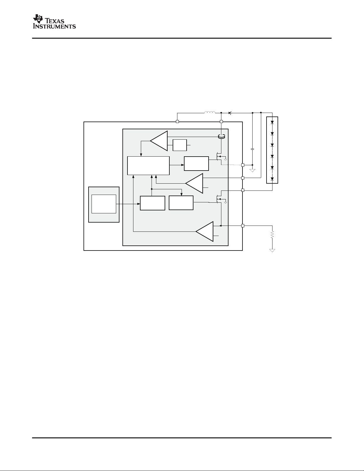
www.ti.com
L3
3.3 Hm
SM3
PGND3
FB3
P3
P3
OUT
GATE
DRIVE
GATE
DRIVE
500 mA
+
_
INDUCTORPEAK
CURRENT
DETECTION
LEDLOWCURRENT
DETECTION
+
_
OUTPUT OVP
DETECTION
+
_
CONTROL LOGIC AND
MINIMUMOFF TIME
MAXIMUMON TIME
SOFT
START
DUTY CYCLE
CONTROL
OFF
OFFON EN
ON
LEDSWITCH
FREQUENCY
ANDDUTY
CYCLE
TPS65810
250 mV
I2CREGISTER
28V
LED
SWITCH
POWER
STAGE
SWITCH
LSM3
D1
SM3_SW
R
10
FB3
W
C27
1 Fm
TPS65810
TPS65811
SLVS658B – MARCH 2006 – REVISED FEBRUARY 2007
WHITE LED CONSTANT CURRENT DRIVER
The TPS65810 has an integrated boost converter (SM3) that is optimized to drive white LEDs connected in a
series configuration. Up to six series white LEDs can be driven, with programmable current and duty cycle
adjustable via a dedicated I2C register.
The SM3 boost converter (SM3) has a 30-V, 500-mA, low-side integrated power stage switch that drives the
external inductor. Another integrated 30-V, 25-mA switch (LED switch) is used to modulate the brightness of the
external white LEDs. A simplified block diagram is shown in Figure 53
Figure 53. Simplified Block Diagram
The SM3 converter operates like a standard boost converter. The LED current is defined by the value of the
external resistor R
, connected from pin FB3 to AGND1. The integrated power stage switch control monitors
FB3
the LED switch current (FB3) and the integrated power stage switch current, implementing a topology that
effectively regulates the LED current independently of the input voltage and number of LEDs connected. The
high voltage rating of the integrated switches enables driving up to six white LEDs, connected in a series
configuration.
The internal LED switch, in series with the external LEDs, disconnects the LEDs from ground during shutdown. In
addition, the LED switch is driven by a PWM signal that sets the duty cycle, enabling adjustment to the average
LED current by modifying the settings of the I2C register SM3_SET. With this control method, the LED brightness
depends on the LED switch duty cycle only, and is independent of the PWM control signal.
The duty cycle control used in the SM3 converter LED switch is implemented by generating a burst of high
frequency pulses, with a pattern that is repeated periodically. For a duty cycle of 50%, all of the high frequency
pulses have a 50% duty cycle. The duty cycle control sets individual pulses to 100% duty cycle when increasing
the LED_PWM output duty cycle; for decreasing LED_PWM output duty cycles, individual pulses are set to 0%
duty cycle. An example of distinct duty cycles is shown in Figure 54 , the sum of the individual pulses on/off time
over the repetition period are equivalent to the duty cycle obtained with traditional single-pulse duty cycle circuits.
Copyright © 2006 – 2007, Texas Instruments Incorporated Submit Documentation Feedback 77
Product Folder Link(s): TPS65810 TPS65811

www.ti.com
SM3CONVERTER
>50%DUTY CYCLE
REPETITIONPERIOD
SM3CONVERTER
50%DUTY CYCLE
SM3CONVERTER
<50%DUTY CYCLE
I
P(typ)
+ I
MAX(L3)
)
V(OUT)
L
100 ns, or : I
P(typ)
+ 500 mA )
V(OUT)
L
100 ns
TPS65810
TPS65811
SLVS658B – MARCH 2006 – REVISED FEBRUARY 2007
Figure 54. Example of Distinct Duty Cycles
The repetition period can be set using the register SOFT_RESET control bit SM3_LF_OSC to either 183 Hz (HI)
or 122 Hz (LO). Each repetition period has a total of 256 pulses, enabling a resolution of 0.4% when
programming the duty cycle.
SM3 Control Logic Overview
The SM3 boost converter operates in a pulse frequency modulation (PFM) scheme with constant peak current
control. This control scheme maintains high efficiency over the entire load current range and enables the use of
small external components, as the switching frequency can reach up to 1 MHz depending on the load conditions.
The LED current ripple is defined by the external inductor size.
The converter monitors the sense voltage at pin FB3, and turns on the integrated power stage switch when V
is below the 250-mV (typ) internal reference voltage and the LED Switch is ON, starting a new cycle. The
integrated power switch turns off when the inductor current reaches the internal 500-mA (typ) peak current limit,
or if the switch is on for a period longer than the maximum on-time of 6 µ s (typ). The integrated power switch
also turns off when the LED switch is set to OFF. As the integrated power switch is turned off, the external
Schottky diode is forward biased, delivering the stored inductor energy to the output. The main switch remains off
until the FB3 pin voltage is below the internal 250-mV reference voltage and the LED switch is turned ON, when
it is turned on again.
This PFM peak current control scheme sets the converter in discontinuous conduction mode (DCM), and the
switching frequency depends on the inductor, input/output voltage and LED current. Lower LED currents reduce
the switching frequency, with high efficiency over the entire LED current range. This regulation scheme is
inherently stable, allowing a wide range for the selection of the inductor and output capacitor.
(FB3)
Peak Current Control (Boost Converter)
The SM3 integrated power stage switch is turned on until the inductor current reaches the dc current limit I
(500 mA, typ). Due to internal delays, typically around 100 ns, the actual current exceeds the DC current limit
threshold by a small amount. The typical peak current limit can be calculated as shown in Equation 8
The current overshoot is directly proportional to the input voltage, and inversely proportional to the inductor
value.
Soft Start
All inductive step-up converters exhibit high in-rush current during start-up. If no special precautions are taken,
voltage drops can be observed at the input supply rail during start-up, with unpredictable results in the overall
system operation.
The SM3 boost converter limits the inrush current during start-up by increasing the current limit in three steps:
1. 125 mA (typ),
2. 250 mA (typ) and
3. 500 mA (typ)
The two initial steps (125 mA and 250 mA) are active for 256 power stage switching cycles.
78 Submit Documentation Feedback Copyright © 2006 – 2007, Texas Instruments Incorporated
Product Folder Link(s): TPS65810 TPS65811
MAX(L3)
(8)

www.ti.com
LED_PWM,>50%DUTY CYCLE
LED_PWM,50%DUTY CYCLE
LED_PWM,<50%DUTY CYCLE
REPETITIONPERIOD
TPS65810
TPS65811
SLVS658B – MARCH 2006 – REVISED FEBRUARY 2007
Enabling the SM3 Converter
The SM3_SET I2C register controls the SM3 LED switch duty cycle. If the register is set to all zeros SM3 is set to
OFF mode. When the host writes a value other than 00 in SM3_SET the SM3 converter is enabled, entering the
soft start phase and then normal operation. The SM3 converter can operate with duty cycles varying from 0.4%
to 99.6%, with LED switch frequencies of 122 Hz or 180 Hz. The LED switch operating frequency is set by bit
SM3_LF, in the SOFT_RESET register.
Overvoltage Protection
The output voltage of the boost converter is sensed at pin SM3, and the integrated power stage switch is turned
OFF when V(SM3) exceeds the internal overvoltage threshold V
when V(SM3) < V
– V
OVP3
HYS(OVP3)
.
Under Voltage Lockout Operation
When the TPS65810 enters the UVLO mode, the SM3 converter is set to OFF mode with the power stage
MOSFET switch and the LED switch open (off).
Thermal Shutdown Operation
When the TPS65810 enters the thermal shutdown mode, the SM3 converter is set to OFF mode with the power
stage MOSFET switch and the LED switch open (off).
. The converter returns to normal operation
OVP3
PWM DRIVERS
PWM Pin Driver
The TPS65810 offers one low-frequency, open-drain PWM driver, capable of driving up to 150 mA. The PWM
frequency and duty cycle are defined by the PWM I2C register settings. The PWM parameters are set in I2C
register PWM. Available frequency values range from 500 Hz to 15 kHz, with 8 frequency values and 16 duty
cycle options (6.25% each).
LED_PWM Pin Driver
The TPS65810 has another PWM driver output (pin LED_PWM), which is optimized to drive a backlight LED.
The LED_PWM driver controls the external LED current intensity using a pulse-width control method, with duty
cycle being set by the I2C register LED_PWM.
The pulse width method implemented generates a burst of high frequency pulses, with a pattern that is repeated
periodically. For a duty cycle of 50%, all of the high -frequency pulses have a 50% duty cycle. The duty cycle
control sets individual pulses to 100% duty cycle when increasing the LED_PWM output duty cycle; for
decreasing LED_PWM output duty cycles individual pulses are set to 0% duty cycle. An example of distinct duty
cycles is shown in Figure 55 ; the sum of the individual pulses on/off time over the repetition period is equivalent
to the duty cycle obtained with traditional single-pulse duty cycle circuits.
The repetition period can be set using the register SOFT_RESET control bit SM3_LF_OSC to either 180 Hz (HI)
or 122 Hz (LO). Each repetition period has a total of 256 pulses, enabling a resoltuion of 0.4% when
programming the duty cycle. The LED_SET register enables control of the duty cycle via I2C, with duty cycle
ranging from 0.4% to 99.6%. Setting the LED_SET register to all zeros forces the LED_PWM pin to 0% duty
cycle (OFF).
Copyright © 2006 – 2007, Texas Instruments Incorporated Submit Documentation Feedback 79
Figure 55. Example of Distinct Duty Cycles
Product Folder Link(s): TPS65810 TPS65811

www.ti.com
GREEN
I
LEDB
RED
BLUE
FLASH
CONTROL
LED
CURRENT
SETTINGS
RGB
DUTY
CYCLE
CONTROL
LED
CONTROL
LOGIC
OUT
R
RED
R
GRN
R
BLUE
I
LEDR
I
LEDG
TPS65810
TPS65811
SLVS658B – MARCH 2006 – REVISED FEBRUARY 2007
RGB Driver
The TPS65810 has a dedicated driver for an RGB external LED. Three outputs are available (pins RED,
GREEN, BLUE), with common settings for operation mode (flash on/off, flash period, flash on time), LED current
and phase delay between outputs. The TPS65810 RGB driver continually flashes the external LEDs connected
to the RED, GREEN and BLUE pins using the flash operation parameters defined in register RGB_FLASH.
The currents for the external LEDs can be programmed via I2C, and external resistors are not required to limit
the LED current. However, they can be added to set the LED current if the available I2C values are not
compatible with the current application, as shown in the circuit below:
Figure 56. Limiting the External LED Current
The flashing-mode parameters defined in register RGB_FLASH enable setting the flashing period from 1 to 8
seconds in 0.5-sec steps, or to continuous operation. Flashing operation is enabled by setting the FLASH_EN bit
in register RGB_FLASH to HI. This bit must be set HI to enable the RGB current-sink channels.
Each driver has an individual duty cycle control. The duty cycle modulation method used is similar to the
PWM_LED duty cycle control, with high frequency pulses being generated when the driver (RED, GREEN, or
BLUE pins) is ON. The repetition period for the RGB drivers has a total of 32 pulses, enabling a 3.125%
resolution when programming the individual RED, GREEN and BLUE drivers duty cycles. The duty cycles for
each driver can be set individually using control bits on registers RGB_RED, RGB_GREEN and RGB_BLUE.
The RGB drivers can be programmed to sink 4, 8, or 12 mA, with no external current limiting resistor.
80 Submit Documentation Feedback Copyright © 2006 – 2007, Texas Instruments Incorporated
Product Folder Link(s): TPS65810 TPS65811

www.ti.com
TPS65810
TPS65811
SLVS658B – MARCH 2006 – REVISED FEBRUARY 2007
White LED, PWM Drivers — I2C Registers
The I2C registers that control LED AND PWM driver related functions are shown below. The HEX address for
each register is shown by the register name, together with the R or W functionality for the register bits. Shaded
values indicate default initial power-up values. In the equations replace Bn with 1 for HI state, and 0 for LO state.
B7 B6 B5 B4 B3 B2 B1 B0
SM3_SET, ADDRESS = 16, ALL BITS R/W
Bit Name SM3_I7 set SM3_I6 set SM3_I5 set SM3_I4 set SM3_I3 set SM3_I2 set SM3_I1 set SM3_I0 set
Function SM3 DUTY CYCLE CONTROL
Value See Table 11 for SM3 duty cycle settings, default = 0 (OFF)
RGB_FLASH, ADDRESS = 17, ALL BITS R/W
Bit Name FLASH_EN FLASH_ON2 FLASH_ON1 FLASH_ON0 FLASH_PER3 FLASH_PER2 FLASH_PER1 FLASH_PER0
Function FLASH MODE FLASH MODE ON TIME FLASH MODE PERIOD
When 0 OFF See Table 12 for RGB ON TIME settings, default = See Table 12 for RGB FLASH settings, default = 1
When 1 ON
RGB_RED, ADDRESS = 18, ALL BITS R/W
Bit Name RGB_ISET1 RGB_ISET0 PHASE PWMR_D4 PWMR_D3 PWMR_D2 PWMR_D1 PWMR_D0
Function RGB LED CURRENT SETTINGS PHASE REG DRIVER DUTY CYCLE CONTROL
When 0 00= 0 10= 8 mA GREEN out of See Table 12 for RGB_RED DUTY settings, default = 0
When 1 BLUE out of Φ
RGB_GREEN, ADDRESS = 19, ALL BITS R/W
Bit Name NOT USED NOT USED NOT USED PWMG_D4 PWMG_D3 PWMG_D2 PWMG_D1 PWMG_D0
Function NOT USED NOT USED NOT USED GREEN DRIVER DUTY CYCLE CONTROL
Value NOT USED NOT USED NOT USED See Table 12 for RGB_GREEN DUTY settings, default = 0
RGB_BLUE, ADDRESS = 1A, ALL BITS R/W
Bit Name NOT USED NOT USED NOT USED PWMB_D4 PWMB_D3 PWMB_D2 PWMB_D1 PWMB_D0
Function NOT USED NOT USED NOT USED BLUE DRIVER DUTY CYCLE CONTROL
Value NOT USED NOT USED NOT USED See Table 12 for RGB_BLUE DUTY settings, default = 0
PWM, ADDRESS = 1D, ALL BITS R/W
Bit Name PWM_EN PWM1_F2 PWM_F1 PWM_F0 PWM_D3 PWM_D2 PWM_D1 PWM_D0
Function PWM ON/OFF PWM DRIVER FREQUENCY SETTINGS PWM DRIVER DUTY CYCLE SETTINGS
When 0 Disabled 000 = 15.6 kHz 011 = 3 kHz 110 = 1 kHz See Table 13 for PWM DUTY settings, default = 0.0625
When 1 Enabled
LED_PWM, ADDRESS = 27, ALL BITS R/W
Bit Name LPWM_7 set LPWM_6 set LPWM_5 set LPWM_4 set LPWM_3 set LPWM_2 set LPWM_1 set LPWM_0 set
Function LED_PWM DRIVER DUTY CYCLE CONTROL
Value See Table 11 for LED_PWM DUTY settings, default = 0 (OFF)
ON/OFF CTRL
0.1
CONTROL
01= 4 mA 11=12 mA Φ with RED &
BLUE
with RED &
GREEN
CONTROL
001 = 7.8 kHz 100 = 2 kHz 111 = 500 Hz
010 = 4.5 kHz 101 = 1.5 kHz Default = 15.6
kHz
Copyright © 2006 – 2007, Texas Instruments Incorporated Submit Documentation Feedback 81
Product Folder Link(s): TPS65810 TPS65811

www.ti.com
TPS65810
TPS65811
SLVS658B – MARCH 2006 – REVISED FEBRUARY 2007
Table 11. SM3 Duty Cycle Settings
Dec B7-B0 Dcpu Dec B7-B0 Dcpu Dec B7-B0 Dcpu Dec B7-B0 Dcpu Dec B7-B0 Dcpu
0 0000 0000 – 52 0011 0100 0.203 104 0110 1000 0.406 156 1001 1100 0.609 208 1101 0000 0.813
1 0000 0001 0.004 53 0011 0101 0.207 105 0110 1001 0.41 157 1001 1101 0.613 209 1101 0001 0.816
2 0000 0010 0.008 54 0011 0110 0.211 106 0110 1010 0.414 158 1001 1110 0.617 210 1101 0010 0.82
3 0000 0011 0.012 55 0011 0111 0.215 107 0110 1011 0.418 159 1001 1111 0.621 211 1101 0011 0.824
4 0000 0100 0.016 56 0011 1000 0.219 108 0110 1100 0.422 160 1010 0000 0.625 212 1101 0100 0.828
5 0000 0101 0.02 57 0011 1001 0.223 109 0110 1101 0.426 161 1010 0001 0.629 213 1101 0101 0.832
6 0000 0110 0.023 58 0011 1010 0.227 110 0110 1110 0.43 162 1010 0010 0.633 214 1101 0110 0.836
7 0000 0111 0.027 59 0011 1011 0.23 111 0110 1111 0.434 163 1010 0011 0.637 215 1101 0111 0.84
8 0000 1000 0.031 60 0011 1100 0.234 112 0111 0000 0.438 164 1010 0100 0.641 216 1101 1000 0.844
9 0000 1001 0.035 61 0011 1101 0.238 113 0111 0001 0.441 165 1010 0101 0.645 217 1101 1001 0.848
10 0000 1010 0.039 62 0011 1110 0.242 114 0111 0010 0.445 166 1010 0110 0.648 218 1101 1010 0.852
11 0000 1011 0.043 63 0011 1111 0.246 115 0111 0011 0.449 167 1010 0111 0.652 219 1101 1011 0.855
12 0000 1100 0.047 64 0100 0000 0.25 116 0111 0100 0.453 168 1010 1000 0.656 220 1101 1100 0.859
13 0000 1101 0.051 65 0100 0001 0.254 117 0111 0101 0.457 169 1010 1001 0.66 221 1101 1101 0.863
14 0000 1110 0.055 66 0100 0010 0.258 118 0111 0110 0.461 170 1010 1010 0.664 222 1101 1110 0.867
15 0000 1111 0.059 67 0100 0011 0.262 119 0111 0111 0.465 171 1010 1011 0.668 223 1101 1111 0.871
16 0001 0000 0.063 68 0100 0100 0.266 120 0111 1000 0.469 172 1010 1100 0.672 224 1110 0000 0.875
17 0001 0001 0.066 69 0100 0101 0.27 121 0111 1001 0.473 173 1010 1101 0.676 225 1110 0001 0.879
18 0001 0010 0.07 70 0100 0110 0.273 122 0111 1010 0.477 174 1010 1110 0.68 226 1110 0010 0.883
19 0001 0011 0.074 71 0100 0111 0.277 123 0111 1011 0.48 175 1010 1111 0.684 227 1110 0011 0.887
20 0001 0100 0.078 72 0100 1000 0.281 124 0111 1100 0.484 176 1011 0000 0.688 228 1110 0100 0.891
21 0001 0101 0.082 73 0100 1001 0.285 125 0111 1101 0.488 177 1011 0001 0.691 229 1110 0101 0.895
22 0001 0110 0.086 74 0100 1010 0.289 126 0111 1110 0.492 178 1011 0010 0.695 230 1110 0110 0.898
23 0001 0111 0.09 75 0100 1011 0.293 127 0111 1111 0.496 179 1011 0011 0.699 231 1110 0111 0.902
24 0001 1000 0.094 76 0100 1100 0.297 128 1000 0000 0.5 180 1011 0100 0.703 232 1110 1000 0.906
25 0001 1001 0.098 77 0100 1101 0.301 129 1000 0001 0.504 181 1011 0101 0.707 233 1110 1001 0.91
26 0001 1010 0.102 78 0100 1110 0.305 130 1000 0010 0.508 182 1011 0110 0.711 234 1110 1010 0.914
27 0001 1011 0.105 79 0100 1111 0.309 131 1000 0011 0.512 183 1011 0111 0.715 235 1110 1011 0.918
28 0001 1100 0.109 80 0101 0000 0.313 132 1000 0100 0.516 184 1011 1000 0.719 236 1110 1100 0.922
29 0001 1101 0.113 81 0101 0001 0.316 133 1000 0101 0.52 185 1011 1001 0.723 237 1110 1101 0.926
30 0001 1110 0.117 82 0101 0010 0.32 134 1000 0110 0.523 186 1011 1010 0.727 238 1110 1110 0.93
31 0001 1111 0.121 83 0101 0011 0.324 135 1000 0111 0.527 187 1011 1011 0.73 239 1110 1111 0.934
32 0010 0000 0.125 84 0101 0100 0.328 136 1000 1000 0.531 188 1011 1100 0.734 240 1111 0000 0.938
33 0010 0001 0.129 85 0101 0101 0.332 137 1000 1001 0.535 189 1011 1101 0.738 241 1111 0001 0.941
34 0010 0010 0.133 86 0101 0110 0.336 138 1000 1010 0.539 190 1011 1110 0.742 242 1111 0010 0.945
35 0010 0011 0.137 87 0101 0111 0.34 139 1000 1011 0.543 191 1011 1111 0.746 243 1111 0011 0.949
36 0010 0100 0.141 88 0101 1000 0.344 140 1000 1100 0.547 192 1100 0000 0.75 244 1111 0100 0.953
37 0010 0101 0.145 89 0101 1001 0.348 141 1000 1101 0.551 193 1100 0001 0.754 245 1111 0101 0.957
38 0010 0110 0.148 90 0101 1010 0.352 142 1000 1110 0.555 194 1100 0010 0.758 246 1111 0110 0.961
39 0010 0111 0.152 91 0101 1011 0.355 143 1000 1111 0.559 195 1100 0011 0.762 247 1111 0111 0.965
40 0010 1000 0.156 92 0101 1100 0.359 144 1001 0000 0.563 196 1100 0100 0.766 248 1111 1000 0.969
41 0010 1001 0.16 93 0101 1101 0.363 145 1001 0001 0.566 197 1100 0101 0.77 249 1111 1001 0.973
42 0010 1010 0.164 94 0101 1110 0.367 146 1001 0010 0.57 198 1100 0110 0.773 250 1111 1010 0.977
43 0010 1011 0.168 95 0101 1111 0.371 147 1001 0011 0.574 199 1100 0111 0.777 251 1111 1011 0.98
44 0010 1100 0.172 96 0110 0000 0.375 148 1001 0100 0.578 200 1100 1000 0.781 252 1111 1100 0.984
45 0010 1101 0.176 97 0110 0001 0.379 149 1001 0101 0.582 201 1100 1001 0.785 253 1111 1101 0.988
46 0010 1110 0.18 98 0110 0010 0.383 150 1001 0110 0.586 202 1100 1010 0.789 254 1111 1110 0.992
47 0010 1111 0.184 99 0110 0011 0.387 151 1001 0111 0.59 203 1100 1011 0.793 255 1111 1111 0.996
48 0011 0000 0.188 100 0110 0100 0.391 152 1001 1000 0.594 204 1100 1100 0.797
49 0011 0001 0.191 101 0110 0101 0.395 153 1001 1001 0.598 205 1100 1101 0.801
50 0011 0010 0.195 102 0110 0110 0.398 154 1001 1010 0.602 206 1100 1110 0.805
51 0011 0011 0.199 103 0110 0111 0.402 155 1001 1011 0.605 207 1100 1111 0.809
82 Submit Documentation Feedback Copyright © 2006 – 2007, Texas Instruments Incorporated
Product Folder Link(s): TPS65810 TPS65811

www.ti.com
TPS65810
TPS65811
SLVS658B – MARCH 2006 – REVISED FEBRUARY 2007
Table 12. RGB Duty Cycle Control Settings
RGB_D4 RGB_D3 RGB_D2 RGB_D1 RGB_D0 DC(%) FLASH_PER3 FLASH_PER2 FLASH_PER1 FLASH_PER0 P(s)
0 0 0 0 0 0.00 0 0 0 0 1
0 0 0 0 1 3.23 0 0 0 1 1.5
0 0 0 1 0 6.45 0 0 1 0 2
0 0 0 1 1 9.68 0 0 1 1 2.5
0 0 1 0 0 12.90 0 1 0 0 3
0 0 1 0 1 16.13 0 1 0 1 3.5
0 0 1 1 0 19.35 0 1 1 0 4
0 0 1 1 1 22.58 0 1 1 1 4.5
0 1 0 0 0 25.80 1 0 0 0 5
0 1 0 0 1 29.03 1 0 0 1 5.5
0 1 0 1 0 32.25 1 0 1 0 6
0 1 0 1 1 35.48 1 0 1 1 6.5
0 1 1 0 0 38.70 1 1 0 0 7
0 1 1 0 1 41.93 1 1 0 1 7.5
0 1 1 1 0 45.15 1 1 1 0 8
0 1 1 1 1 48.38 1 1 1 1 Continuous
1 0 0 0 0 51.60
1 0 0 0 1 54.83
1 0 0 1 0 58.05 FLASH_ON2 FLASH_ON1 FLASH_ON0 ON_TIME (s)
1 0 0 1 1 61.23 0 0 0 0.1
1 0 1 0 0 64.50 0 0 1 0.15
1 0 1 0 1 67.73 0 1 0 0.2
1 0 1 1 0 70.95 0 1 1 0.25
1 0 1 1 1 74.18 1 0 0 0.3
1 1 0 0 0 77.40 1 0 1 0.4
1 1 0 0 1 80.63 1 1 0 0.5
1 1 0 1 0 83.85 1 1 1 0.6
1 1 0 1 1 87.08
1 1 1 0 0 90.30
1 1 1 0 1 93.53
1 1 1 1 0 96.75
1 1 1 1 1 99.98
Copyright © 2006 – 2007, Texas Instruments Incorporated Submit Documentation Feedback 83
Product Folder Link(s): TPS65810 TPS65811

www.ti.com
TPS65810
TPS65811
SLVS658B – MARCH 2006 – REVISED FEBRUARY 2007
Table 13. PWM Frequency and Duty Cycle Settings
PWM FREQUENCY TABLE PWM_D DUTY CYCLE
PWM_F2 PWM_F1 PWM_F0 F (Hz) PWM2_D3 PWM2_D2 PWM2_D1 PWM2_D0 D_cycle (pu)
0 0 0 15600 0 0 0 0 0.0625
0 0 1 7800 0 0 0 1 0.125
0 1 0 4500 0 0 1 0 0.1875
0 1 1 3000 0 0 1 1 0.25
1 0 0 2000 0 1 0 0 0.3125
1 0 1 1500 0 1 0 1 0.375
1 1 0 1000 0 1 1 0 0.4375
1 1 1 500 0 1 1 1 0.5
1 0 0 0 0.5625
1 0 0 1 0.625
1 0 1 0 0.6875
1 0 1 1 0.75
1 1 0 0 0.8125
1 1 0 1 0.875
1 1 1 0 0.9375
1 1 1 1 1
84 Submit Documentation Feedback Copyright © 2006 – 2007, Texas Instruments Incorporated
Product Folder Link(s): TPS65810 TPS65811

www.ti.com
GPIO1
GPIO
CONTROL
GPIO2
GPIO3
I2C
SETTINGS
GPIO
FUNCTION
ANDMODE
TPS65810
CONFIGURATIONMODES:
1-OUTPUT
2-ADC TRIGGERCONTROL
3-LDC0ENABLE
4-CHARGEVOLTAGESELECTION
CONFIGURATIONMODES:
1-OUTPUT
2-SM1/SM2STANDBY CONTROL INPUT
3-SM1ON/OFFCONTROL INPUT
4-INTERRUPT REQUEST CONTROL INPUT
GENERATES PINHI LO TRANSITIONINT ®
CONFIGURATIONMODES:
1-OUTPUT
2-SM2 CONTROL
34-GENERATES PINHI LO TRANSITION
ON/OFF
INTERRUPT REQUEST CONTROL INPUT
INT ®
SLVS658B – MARCH 2006 – REVISED FEBRUARY 2007
FUNCTIONALITY GUIDE – GENERAL PURPOSE INPUTS/OUTPUTS
GPIO3 FUNCTIONS
CONFIGURED AS OUTPUT CONFIGURED AS INPUT POWER-UP
OUTPUT LEVEL Io(max) A/D CONVERSION START TRIGGER
mA
HI or LO at output set 5 Falling or rising edge selected via I2C Input, no mode
via I2C selected
GPIO2 FUNCTIONS
CONFIGURED AS OUTPUT CONFIGURED AS INPUT POWER-UP
OUTPUT LEVEL Io(max) HOST INTERRUPT SM2 ENABLE
mA REQUEST
HI or LO at output set 5 Set INT pin to LO via I2C GPIO2 level sets SM2 converter ON/OFF operation. Input, SM2
via I2C when GPIO2 pin edge is GPIO2 pin level (HI or LO) for ON operation enable, SM2
detected. Rising or falling selected via I2C ON@
edge detection selected via GPIO2=HI
I2C
The host interrupt request and SM2 enable GPIO2 functions are mutually exclusive,
and they should NOT be configured simultaneously
GPIO1 FUNCTIONS
CONFIGURED AS OUTPUT CONFIGURED AS INPUT POWER-UP
OUTPUT LEVEL Io(max) HOST INTERRUPT SM1 ENABLE SM1 AND SM2 STANDBY
mA REQUEST CONTROL
HI or LO at output set 5 Set INT pin to LO via I2C GPIO1 level sets SM1 GPIO1 level sets SM2 and Input, SM1
via I2C when GPIO1 pin edge is converter ON/OFF SM1 converters in standby enable, SM1
detected. Rising or falling operation. GPIO2 pin mode. GPIO1 pin level (HI ON@
edge detection set via I2C level (HI or LO) for ON or LO) for standby mode GPIO1=HI
operation set via I2C set selected via I2C
The host interrupt request, SM1 enable and SM1/SM2 standby control GPIO1
functions are mutually exclusive, and they should NOT be configured simultaneously.
TPS65810
TPS65811
DEFAULT
DEFAULT
DEFAULT
Figure 57. Required External Components, Recommended Values, External Connections
Copyright © 2006 – 2007, Texas Instruments Incorporated Submit Documentation Feedback 85
Product Folder Link(s): TPS65810 TPS65811

www.ti.com
S1
S2
D
C ENB
Multiplexer
Q
Q
SET
CLR
D
GPIO
SignalPin
HI=RisingEdge,
LO=FallingEdge
UVLO
GPIOConfig= OUTPUT
Equivalentcircuitforinternal
logicwhenconfiguredasedge
interruptwithnomasking
I CINTACKREAD
C
2
ommand?
INT INT
TPS65810
TPS65811
SLVS658B – MARCH 2006 – REVISED FEBRUARY 2007
General Purpose I/Os — GPIO 1, 2, 3
The TPS65810 integrates 3 general purpose open drain ports (GPIOs) that can be configured as selectable
inputs or outputs. When configured as outputs the output level can be set to LO or HI via I2C commands. When
the GPIOs are configured as inputs the action to be taken when a transition or HI/LO level is detected at the
GPIO pin is selectable via I2C.
When configured as inputs the GPIOs can be set in the following modes:
1. Interrupt request: In this mode of operation, a transition at the GPIO pin generates an interrupt request at the
interrupt controller. The GPIO interrupt request can be masked at the INT_MASK register. This operation
mode is available for GPIO ’ s 1 and 2.
2. SM1 and SM2 control: The GPIO ’ s can be used to turn the converters SM1 and SM2 ON/OFF, as well as
setting them in standby mode. This control mode is available for GPIO1 (SM1 on/off and SM1/SM2 standby)
and GPIO2 (SM2 on/off control).
3. ADC trigger: GPIO3 can be configured as an external ADC trigger. The GPIO3 trigger configuration bit is
located at the ADC register ADC_DELAY.
GPIOs Input Level Configuration
When using I2C commands, the GPIO1 and GPIO2 pins can be configured as logic output signals or as
level-controlled inputs which enables (or disables) the switch mode converters SM1 and/or SM2. These pins may
also be configured as rising- or falling-edge-triggered inputs to externally control the generation of an interrupt
signal ( INT), if desired.
The GPIO3 pin may be used as an external trigger source to start an A/D conversion cycle or as a logic output.
See Figure 58 for a description of the logic used for GPIO1 and GPIO2 inputs when configured for
edge-triggered interrupt generation. The signal from the GPIO pin input is double-latched before being sent to the
interrupt contoller logic. The inversion of the Q output from the first flip-flop must be HI to allow the output latch to
be cleared when a READ command occurs. On the initial edge of the GPIO signal, the Q output of the flip-flop is
set (HI). The INT line is asserted (LO) after the initial selected edge from the GPIO pin. On the next falling (or
rising) edge of the GPIO pin, the interrupt can again be cleared (which allows the INT pin to go back high). The
INT signal is cleared (set back HI) after an I2C READ operation is performed.
Thus, two successive edges of the GPIO signal, followed by an I2C READ command, are required to clear the
INT pin output. If no I2C READ commands occur, repeatedly applying edges to the GPIO pin does not toggle the
state of the INT pin output.
In addition to an I2C READ command after two GPIO edges, a UVLO event or reconfiguration of the GPIO pins
as outputs also de-asserts the INT signal.
Figure 58. GPIO 1 or GPIO2 Configured as an Interrupt Request Input
86 Submit Documentation Feedback Copyright © 2006 – 2007, Texas Instruments Incorporated
Product Folder Link(s): TPS65810 TPS65811

www.ti.com
TPS65810
TPS65811
SLVS658B – MARCH 2006 – REVISED FEBRUARY 2007
Function Implementation: I2C Commands Versus GPIO Commands
Some of the GPIO SM1/SM2 control functions overlap I2C register control functions. Table 14 describes the
TPS65810 action when the GPIO ’ s command and I2C registers commands are not compatible with each other.
Table 14. GPIO Commands and I2C Registers Commands
SM1 AND SM2 ON/OFF I2C COMMAND GPIO COMMAND SM1 OR SM2 MODE SET
CONVERTER DISABLED CONVERTER DISABLED DISABLED
CONVERTER ENABLED DON ’ T CARE ENABLED
DON ’ T CARE CONVERTER ENABLED ENABLED
SM1 AND SM2 STANDBY I2C COMMAND GPIO COMMAND SM1 OR SM2 MODE SET
DO NOT SET STANDBY DON ’ T CARE NORMAL
SET STANDBY SET STANDBY STANDBY
DON ’ T CARE DO NOT SET STANDBY NORMAL
Copyright © 2006 – 2007, Texas Instruments Incorporated Submit Documentation Feedback 87
Product Folder Link(s): TPS65810 TPS65811

www.ti.com
TPS65810
TPS65811
SLVS658B – MARCH 2006 – REVISED FEBRUARY 2007
GPIO Configuration Table
Table 15 describes the I2C register settings required to program the available GPIO modes. The GPIO pins logic
level is available at register SM1_STANDBY, bits B5, B6 and B7.
Table 15. Recommended GPIO Configuration Procedure
GPIO MODE I2C I2C REGISTER BIT SETTING ADDITIONAL DETAILS
GPIO3 = OUTPUT GPIO3 GPIO3I/O=HI AND GPIO3OUT=HI GPIO3 PIN SET TO HIGH IMPEDANCE
GPIO3 =INPUT GPIO3 AND GPIO3I/O=LO AND ADC_TRG_GPIO3=HI AND GPIO3 pin rising edge triggers ADC
ADC CONVERSION ADC_DELAY EDGE_GPIO3=HI conversion
START TRIGGER
GPIO2 = OUTPUT GPIO12 GPIO2I/O=HI AND GPIO2OUT=HI GPIO2 PIN SET TO HIGH IMPEDANCE
GPIO2=INPUT, GPIO12 AND GPIO2I/O=LO AND GPIO2INT=HI AND INT pin HI → LO → HI at V(GPIO2) falling
HOST INTERRUPT GPIO3 GPIO2LVL=HI AND GPIO2SM2=LO edge
REQUEST
GPIO2=INPUT, GPIO12 AND GPIO2I/O=LO AND GPIO2INT=LO AND SM2 converter ON at V(GPIO2)=HI
SM2 ENABLE GPIO3 GPIO2LVL=HI AND GPIO2SM2=HI
GPIO1 = OUTPUT GPIO12 GPIO1I/O=HI AND GPIO1OUT=HI GPIO1 PIN SET TO HIGH IMPEDANCE
GPIO1=INPUT, GPIO12 AND GPIO1I/O=LO AND GPIO1INT=HI AND INT pin HI → LO → HI at V(GPIO1) falling
HOST INTERRUPT GPIO3 GPIO1LVL=HI AND GPIO1SM1=LO AND edge
REQUEST GPIO1SMSBY=LO
GPIO1=INPUT, GPIO12 AND GPIO1I/O=LO AND GPIO1INT=LO AND SM1 converter ON at V(GPIO1)=HI
SM1 ENABLE GPIO3 GPIO1LVL=HI AND GPIO1SM1=HI AND
GPIO1=INPUT, GPIO12 AND GPIO1I/O=LO AND GPIO1INT=LO AND SM1/SM2 converter standby set at
SM1/SM2 STANDBY GPIO3 GPIO1LVL=HI AND GPIO1SM1=LO AND V(GPIO1) = HI
CONTROL GPIO1SMSBY=HI
REGISTERS
MODE
GPIO3I/O=HI AND GPIO3OUT=LO V(GPIO3) = V
GPIO3I/O=LO AND ADC_TRG_GPIO3=HI AND GPIO3 pin falling edge triggers ADC
EDGE_GPIO3=LO conversion
MODE
GPIO2I/O=HI AND GPIO2OUT=LO V(GPIO2) = V
GPIO2I/O=LO AND GPIO2INT=HI AND INT pin HI → LO → HI at V(GPIO2) rising
GPIO2LVL=HI AND GPIO2SM2=LO edge
GPIO2I/O=LO AND GPIO2INT=LO AND SM2 converter ON at V(GPIO2)=LO
GPIO2LVL=LO AND GPIO2SM2=HI
MODE
GPIO1I/O=HI AND GPIO1OUT=LO V(GPIO1) = V
GPIO1I/O=LO AND GPIO1INT=HI AND INT pin HI → LO → HI at V(GPIO1) rising
GPIO1LVL=LO AND GPIO1SM1=LO AND edge
GPIO1SMSBY=LO
GPIO1SMSBY=LO
GPIO1I/O=LO AND GPIO1INT=LO AND SM1 converter ON at V(GPIO1)=LO
GPIO1LVL=LO AND GPIO1SM1=HI AND
GPIO1SMSBY=LO
GPIO1I/O=LO AND GPIO1INT=LO AND SM1/SM2 converter standby set at
GPIO1LVL=LO AND GPIO1SM1=LO AND V(GPIO1) = LO
GPIO1SMSBY=HI
OL
OL
OL
88 Submit Documentation Feedback Copyright © 2006 – 2007, Texas Instruments Incorporated
Product Folder Link(s): TPS65810 TPS65811
www.ti.com
TPS65810
TPS65811
SLVS658B – MARCH 2006 – REVISED FEBRUARY 2007
GPIOs — I2C Registers
The I2C registers that control GPIO-related functions are shown below. The HEX address for each register is
shown by the register name, together with the R or W functionality for the register bits. Shaded values indicate
default initial power-up values.
B7 B6 B5 B4 B3 B2 B1 B0
GPIO12, ADDRESS=1B, ALL BITS R/W
Bit Name GPIO2I/O GPIO1I/O GPIO2OUT GPIO1OUT GPIO2LVL GPIO1LVL GPIO1SMSBY GPIO1SM1
Function GPIO2 MODE GPIO1 MODE SET GPIO2 SET GPIO1 GPIO2 EDGE GPIO1 EDGE GPIO 1 GPIO1
When 0 INPUT INPUT LOW LOW RISING EDGE, RISING EDGE, DISABLED DISABLED
When 1 OUTPUT OUTPUT HIGH HIGH FALLING FALLING ENABLED ENABLED
GPIO3, ADDRESS=1C, ALL BITS R/W
Bit Name GPIO3I/O GPIO3OUT LDO0_EN CHG_VOLT NOT USED GPIO2 INT GPIO1 INT GPIO2SM2
Function GPIO3 MODE SET GPIO3 LDO0 ON/OFF CHARGE NOT USED GPIO2 GPIO1 SM2 ON/OFF
LEVEL CONTROL VOLTAGE TRIGGERS TRIGGERS CONTROL
(OUTPUT SAFETY BIT INT:HI → LO INT:HI → LO
ONLY)
When 0 INPUT LOW OFF 4.20 V NOT USED DISABLED DISABLED DISABLED
When 1 OUTPUT HIGH ON 4.36 V NOT USED ENABLED ENABLED ENABLED
LEVEL LEVEL AND LEVEL AND LEVEL CONTROLS CONTROLS
(OUTPUT (OUTPUT DETECTION DETECTION SM1 AND SM2 SM1 ON/OFF
ONLY) ONLY) STANDBY
ON/OFF
LO LEVEL LO LEVEL
EDGE, HI EDGE, HI
LEVEL LEVEL
Copyright © 2006 – 2007, Texas Instruments Incorporated Submit Documentation Feedback 89
Product Folder Link(s): TPS65810 TPS65811

www.ti.com
F +
1
2p LC
Ǹ
+ 27.7 kHz (a) for L + 3.3 mH andC + 10 mF
I
target
+
V
OUT
0.3 I
OUT_MAX
ǒ
1 *
V
OUT
V
IN_MAX
Ǔ
f
DI
L
+
V
L
L
Dt +
V
OUT
L
ǒ
1 *
V
OUT
V
IN
Ǔ
f
I
Lmax
+ I
OUTmax
)
DI
L
2
TPS65810
TPS65811
SLVS658B – MARCH 2006 – REVISED FEBRUARY 2007
APPLICATION INFORMATION
INDUCTOR AND CAPACITOR SELECTION — CONVERTERS SM1 AND SM2
SM1 and SM2 are designed with internal voltage mode compensation and the stabilization is based on choosing
an LC filter that has a corner frequency around 27 kHz. It is not recommended to use LC values that would be
outside the range of 13 kHz to 40 kHz.
Equation 9 calculates the corner frequency of the output LC filter. The standard recommended LC values are 3.3
µ H and 10 µ F.
The inductor value, along with the input voltage VIN, output voltage V
ripple current. Typically the ripple current target is 30% of the full load current. At light loads it is desirable for
ripple current to be less then 150% of the light load current.
The inductor should be chosen with a rating to handle the peak ripple current., if an inductor ’ s current gets higher
than its rated saturation level (DCR), the inductance starts to fall off, and the inductor ’ s ripple current increases
exponentially. The DCR of the inductor plays an important role in efficiency and size of the inductor. Larger
diameter wire has less DCR but may increase the size of the inductor
Equation 10 calculates the target inductor value. If an inductor value has already been chosen, Equation 11 ,
calculates the inductor ’ s ripple current under static operating conditions. The ripple amplitude can be calculated
during the on time (positive ramp) or during the off time (negative ramp). It is easiest to calculate the ripple using
the off time since the inductor ’ s voltage is the output voltage.
and switching frequency f define the
OUT
(9)
Equation 12 calculates the peak current due to the output load and ripple current
For a faster transient response, a lower inductor and higher capacitance allows the output current to ramp faster,
while the addition capacitance holds up the output longer (a 2.2- µ H inductor in combination with a 22- µ F output
capacitor are recommended).
The highest inductor current occurs at the maximum input voltage. The peak inductor current during a transient
may be higher than the steady state peak current and should be considered when choosing an inductor.
Monitoring the inductor current for non-saturation operation during a transient of 1.2 × I_loadmax at Vin_max
ensures adequate saturation margin.
Table 16. Inductors for Typical Operation Conditions
DEVICE INDUCTOR VALUE TYPE COMPONENT SUPPLIER
DCDC3 converter 3.3 µ H CDRH2D14NP-3R3 Sumida
3.3 µ H PDS3010-332 Coilcraft
3.3 µ H VLF4012AT-3R3M1R3 TDK
2.2 µ H VLF4012AT-2R2M1R5 TDK
2.2 µ H NR3015T2R2 Taoup-Uidem
(10)
(11)
(12)
90 Submit Documentation Feedback Copyright © 2006 – 2007, Texas Instruments Incorporated
Product Folder Link(s): TPS65810 TPS65811

www.ti.com
I
RMSCout
+
1 *
V
OUT
V
IN
2 L f
1
3
Ǹ
V
RMSCout
+
1 *
V
OUT
V
IN
L f
ǒ
1
8 Cout f
) ESR
Ǔ
TPS65810
TPS65811
SLVS658B – MARCH 2006 – REVISED FEBRUARY 2007
Table 16. Inductors for Typical Operation Conditions (continued)
DEVICE INDUCTOR VALUE TYPE COMPONENT SUPPLIER
DCDC2 converter 3.3 µ H CDRH2D18/HPNP-3R3 Sumida
3.3 µ H VLF4012AT-3R3M1R3 TDK
2.2 µ H VLCF4020-2R2 TDK
DCDC1 converter 3.3 µ H CDRH3D14/HPNP-3R2 Sumida
3.3 µ H CDRH4D28C-3R2 Sumida
3.3 µ H MSS5131-332 Coilcraft
2.2 µ H VLCF4020-2R2 TDK
OUTPUT CAPACITOR SELECTION, SM1, SM2 CONVERTERS
The advanced Fast Response voltage mode control scheme of the SM1, SM2 converters implemented in the
TPS65020 allow the use of small ceramic capacitors with a typical value of 10 µ F for a 3.3- µ H inductor, without
having large output voltage under and overshoots during heavy load transients.
Ceramic capacitors having low ESR values have low output voltage ripple, and recommended values and
manufacturers are listed in Table 1 . Often, due to the low ESR, the ripple current rating of the ceramic capacitor
is adequate to meet the inductor ’ s currents requirements.
The RMS ripple current is calculated as:
At nominal load current, the inductive converters operate in PWM mode. The overall output voltage ripple is the
sum of the voltage spike caused by the output capacitor ESR plus the voltage ripple caused by charging and
discharging the output capacitor: The output voltage ripple is maximum at the highest input voltage Vin.
At light load currents, the converters operate in PFM and the output voltage ripple is dependent on the output
capacitor value. The output voltage ripple is set by the internal PFM output voltage comparator delay and the
external capacitor. The typical output voltage ripple is less than 1% of the nominal output voltage.
Table 17. Input/Output Capacitors for Typical Operation Conditions
CAPACITOR VALUE CASE SIZE COMPONENT SUPPLIER COMMENTS
22 µ F 1260 TDK C3216X5R0J226M Ceramic
22 µ F 1260 Taiyo Yuden JMK316BJ226ML Ceramic
10 µ F 0805 Taiyo Yuden JMK212BJ106M Ceramic
10 µ F 0805 TDK C2012X5R0J106M Ceramic
22 µ F 0805 TDK C2012X5R0J226MT Ceramic
22 µ F 0805 Taiyo Yuden JMK212BJ226MG Ceramic
(13)
(14)
Copyright © 2006 – 2007, Texas Instruments Incorporated Submit Documentation Feedback 91
Product Folder Link(s): TPS65810 TPS65811

www.ti.com
R1 +
ƪ
V
SMxOUT
V
FB
* 1ƫR2
L
target
+
V
OUT
0.3 I
OUT_MAX
ƪ
1 *
V
OUT
V
IN_MAX
ƫ
fsw
+ 3.35 mH, 3.3 mH is a good target.
C +
1
L[2 p fc]
2
+ 10.5 mF 10 mF is a good target.
R
ISET
+
K
SET
V
SET
I
PGM
+ 1 kW
R
DPPM
+
V
DPPM_OUT
K
DPPM
I
DPPM
+ 3.74 kW
TPS65810
TPS65811
SLVS658B – MARCH 2006 – REVISED FEBRUARY 2007
INPUT CAPACITOR SELECTION, SM1, SM2 CONVERTERS
Buck converters have a pulsating input current that can generate high input voltage spikes at V
input capacitor is required to filter the input voltage, minimizing the interference with other circuits connected to
the same power supply rail. Each dc-dc converter requires a 10- µ F ceramic input capacitor on its input pin.
OUTPUT VOLTAGE SELECTION, SM1, SM2 CONVERTERS
Typically the output voltage is programmed by the I2C. An external divider can be added to raise the output
voltage, if the available I2C values do not meet the application requirements. Care must be taken with this special
option, because this external divider (gain factor) would apply to any selected I2C output voltage value for this
converter.
Equation 16 calculates R1, Let R2 = 20 k Ω :
where V
is the I2C selected voltage, is the desired output voltage and R1/R2 is the feedback divider.
FB
DESIGN EXAMPLES
SM1, SM2 CONVERTER DESIGN EXAMPLE
IN
. A low ESR
(16)
Design Conditions and Parametrs for SM1 or SM2:
Vin_SM1/2: 4.6 V typical (may be less if input source is limited).
Vout_SM1/2: 1.24 V
Iout_max: 0.6 A
fsw = 1500 kHz
fc = 25 kHz
CHARGER DESIGN EXAMPLE
Design Conditions and Parameters for Charger:
Vout: 4.6 V; (OUT pin is input to charger)
Fast-charge current, I
: 1 A
PGM
DPPM-OUT threshold: 4.3 V; (charging current reduces when OUT falls to this level)
Safety timer: 5 h
Battery short-circuit delay, t
: 47 µ s; (delays BAT short circuit during hot plug of battery)
DELAY
TS temperature range: disabled
K
SET
= 400; V
SET
= 2.5 V; K
DPPM
= 1.15; I
DPPM
= 100 µ A; K
TMR
= 0.36 s/ Ω
Program Fast Charge Current Level:
(17)
(18)
Program DPPM_OUT Voltage Level (Level at Which Charging Current Reduces)
92 Submit Documentation Feedback Copyright © 2006 – 2007, Texas Instruments Incorporated
Product Folder Link(s): TPS65810 TPS65811
(19)
(20)

www.ti.com
C
DPPM
+ t
DELAY
I
DPPM
+ 4.7 Nf
R
TMR
+
t
SAFETY*HR
3600 secńhr
K
TMR
+ 50 kW
Program BAT Short Circuit Delay (Used for inserting battery)
Program 5-Hour Safety Timer
TPS65810
TPS65811
SLVS658B – MARCH 2006 – REVISED FEBRUARY 2007
(21)
(22)
Copyright © 2006 – 2007, Texas Instruments Incorporated Submit Documentation Feedback 93
Product Folder Link(s): TPS65810 TPS65811

PACKAGE OPTION ADDENDUM
www.ti.com
25-Sep-2007
PACKAGING INFORMATION
Orderable Device Status
(1)
Package
Type
Package
Drawing
Pins Package
Qty
Eco Plan
TPS65810RTQR ACTIVE QFN RTQ 56 2000 Green (RoHS &
no Sb/Br)
TPS65810RTQRG4 ACTIVE QFN RTQ 56 2000 Green (RoHS &
no Sb/Br)
TPS65810RTQT ACTIVE QFN RTQ 56 250 Green (RoHS &
no Sb/Br)
TPS65810RTQTG4 ACTIVE QFN RTQ 56 250 Green (RoHS &
no Sb/Br)
TPS65811RTQR ACTIVE QFN RTQ 56 2000 Green (RoHS &
no Sb/Br)
TPS65811RTQRG4 ACTIVE QFN RTQ 56 2000 Green (RoHS &
no Sb/Br)
TPS65811RTQT ACTIVE QFN RTQ 56 250 Green (RoHS &
no Sb/Br)
TPS65811RTQTG4 ACTIVE QFN RTQ 56 250 Green (RoHS &
no Sb/Br)
(1)
The marketing status values are defined as follows:
ACTIVE: Product device recommended for new designs.
LIFEBUY: TI has announced that the device will be discontinued, and a lifetime-buy period is in effect.
NRND: Not recommended for new designs. Device is in production to support existing customers, but TI does not recommend using this part in
a new design.
PREVIEW: Device has been announced but is not in production. Samples may or may not be available.
OBSOLETE: TI has discontinued the production of the device.
(2)
Lead/Ball Finish MSL Peak Temp
CU NIPDAU Level-3-260C-168 HR
CU NIPDAU Level-3-260C-168 HR
CU NIPDAU Level-3-260C-168 HR
CU NIPDAU Level-3-260C-168 HR
CU NIPDAU Level-3-260C-168 HR
CU NIPDAU Level-3-260C-168 HR
CU NIPDAU Level-3-260C-168 HR
CU NIPDAU Level-3-260C-168 HR
(3)
(2)
Eco Plan - The planned eco-friendly classification: Pb-Free (RoHS), Pb-Free (RoHS Exempt), or Green (RoHS & no Sb/Br) - please check
http://www.ti.com/productcontent for the latest availability information and additional product content details.
TBD: The Pb-Free/Green conversion plan has not been defined.
Pb-Free (RoHS): TI's terms "Lead-Free" or "Pb-Free" mean semiconductor products that are compatible with the current RoHS requirements
for all 6 substances, including the requirement that lead not exceed 0.1% by weight in homogeneous materials. Where designed to be soldered
at high temperatures, TI Pb-Free products are suitable for use in specified lead-free processes.
Pb-Free (RoHS Exempt): This component has a RoHS exemption for either 1) lead-based flip-chip solder bumps used between the die and
package, or 2) lead-based die adhesive used between the die and leadframe. The component is otherwise considered Pb-Free (RoHS
compatible) as defined above.
Green (RoHS & no Sb/Br): TI defines "Green" to mean Pb-Free (RoHS compatible), and free of Bromine (Br) and Antimony (Sb) based flame
retardants (Br or Sb do not exceed 0.1% by weight in homogeneous material)
(3)
MSL, Peak Temp. -- The Moisture Sensitivity Level rating according to the JEDEC industry standard classifications, and peak solder
temperature.
Important Information and Disclaimer:The information provided on this page represents TI's knowledge and belief as of the date that it is
provided. TI bases its knowledge and belief on information provided by third parties, and makes no representation or warranty as to the
accuracy of such information. Efforts are underway to better integrate information from third parties. TI has taken and continues to take
reasonable steps to provide representative and accurate information but may not have conducted destructive testing or chemical analysis on
incoming materials and chemicals. TI and TI suppliers consider certain information to be proprietary, and thus CAS numbers and other limited
information may not be available for release.
In no event shall TI's liability arising out of such information exceed the total purchase price of the TI part(s) at issue in this document sold by TI
to Customer on an annual basis.
Addendum-Page 1

PACKAGE MATERIALS INFORMATION
www.ti.com
TAPE AND REEL INFORMATION
11-Mar-2008
*All dimensions are nominal
Device Package
TPS65810RTQR QFN RTQ 56 2000 330.0 16.4 8.3 8.3 2.25 12.0 16.0 Q2
TPS65810RTQT QFN RTQ 56 250 180.0 16.4 8.3 8.3 2.25 12.0 16.0 Q2
TPS65811RTQR QFN RTQ 56 2000 330.0 16.4 8.3 8.3 2.25 12.0 16.0 Q2
TPS65811RTQT QFN RTQ 56 250 180.0 16.4 8.3 8.3 2.25 12.0 16.0 Q2
Type
Package
Drawing
Pins SPQ Reel
Diameter
(mm)
Reel
Width
W1 (mm)
A0 (mm) B0 (mm) K0 (mm) P1
(mm)W(mm)
Pin1
Quadrant
Pack Materials-Page 1
PACKAGE MATERIALS INFORMATION
www.ti.com
11-Mar-2008
*All dimensions are nominal
Device Package Type Package Drawing Pins SPQ Length (mm) Width (mm) Height (mm)
TPS65810RTQR QFN RTQ 56 2000 346.0 346.0 33.0
TPS65810RTQT QFN RTQ 56 250 190.5 212.7 31.8
TPS65811RTQR QFN RTQ 56 2000 346.0 346.0 33.0
TPS65811RTQT QFN RTQ 56 250 190.5 212.7 31.8
Pack Materials-Page 2


IMPORTANT NOTICE
Texas Instruments Incorporated and its subsidiaries (TI) reserve the right to make corrections, modifications, enhancements, improvements,
and other changes to its products and services at any time and to discontinue any product or service without notice. Customers should
obtain the latest relevant information before placing orders and should verify that such information is current and complete. All products are
sold subject to TI’s terms and conditions of sale supplied at the time of order acknowledgment.
TI warrants performance of its hardware products to the specifications applicable at the time of sale in accordance with TI’s standard
warranty. Testing and other quality control techniques are used to the extent TI deems necessary to support this warranty. Except where
mandated by government requirements, testing of all parameters of each product is not necessarily performed.
TI assumes no liability for applications assistance or customer product design. Customers are responsible for their products and
applications using TI components. To minimize the risks associated with customer products and applications, customers should provide
adequate design and operating safeguards.
TI does not warrant or represent that any license, either express or implied, is granted under any TI patent right, copyright, mask work right,
or other TI intellectual property right relating to any combination, machine, or process in which TI products or services are used. Information
published by TI regarding third-party products or services does not constitute a license from TI to use such products or services or a
warranty or endorsement thereof. Use of such information may require a license from a third party under the patents or other intellectual
property of the third party, or a license from TI under the patents or other intellectual property of TI.
Reproduction of TI information in TI data books or data sheets is permissible only if reproduction is without alteration and is accompanied
by all associated warranties, conditions, limitations, and notices. Reproduction of this information with alteration is an unfair and deceptive
business practice. TI is not responsible or liable for such altered documentation. Information of third parties may be subject to additional
restrictions.
Resale of TI products or services with statements different from or beyond the parameters stated by TI for that product or service voids all
express and any implied warranties for the associated TI product or service and is an unfair and deceptive business practice. TI is not
responsible or liable for any such statements.
TI products are not authorized for use in safety-critical applications (such as life support) where a failure of the TI product would reasonably
be expected to cause severe personal injury or death, unless officers of the parties have executed an agreement specifically governing
such use. Buyers represent that they have all necessary expertise in the safety and regulatory ramifications of their applications, and
acknowledge and agree that they are solely responsible for all legal, regulatory and safety-related requirements concerning their products
and any use of TI products in such safety-critical applications, notwithstanding any applications-related information or support that may be
provided by TI. Further, Buyers must fully indemnify TI and its representatives against any damages arising out of the use of TI products in
such safety-critical applications.
TI products are neither designed nor intended for use in military/aerospace applications or environments unless the TI products are
specifically designated by TI as military-grade or "enhanced plastic." Only products designated by TI as military-grade meet military
specifications. Buyers acknowledge and agree that any such use of TI products which TI has not designated as military-grade is solely at
the Buyer's risk, and that they are solely responsible for compliance with all legal and regulatory requirements in connection with such use.
TI products are neither designed nor intended for use in automotive applications or environments unless the specific TI products are
designated by TI as compliant with ISO/TS 16949 requirements. Buyers acknowledge and agree that, if they use any non-designated
products in automotive applications, TI will not be responsible for any failure to meet such requirements.
Following are URLs where you can obtain information on other Texas Instruments products and application solutions:
Products Applications
Amplifiers amplifier.ti.com Audio www.ti.com/audio
Data Converters dataconverter.ti.com Automotive www.ti.com/automotive
DSP dsp.ti.com Broadband www.ti.com/broadband
Clocks and Timers www.ti.com/clocks Digital Control www.ti.com/digitalcontrol
Interface interface.ti.com Medical www.ti.com/medical
Logic logic.ti.com Military www.ti.com/military
Power Mgmt power.ti.com Optical Networking www.ti.com/opticalnetwork
Microcontrollers microcontroller.ti.com Security www.ti.com/security
RFID www.ti-rfid.com Telephony www.ti.com/telephony
RF/IF and ZigBee® Solutions www.ti.com/lprf Video & Imaging www.ti.com/video
Mailing Address: Texas Instruments, Post Office Box 655303, Dallas, Texas 75265
Copyright © 2008, Texas Instruments Incorporated
Wireless www.ti.com/wireless
 Loading...