

www.ti.com
SWN
TPS65123
D1
L1
10
C1
2.2
V
IN
2.7 V to 5.5 V
V
GL
down to −18 V/2 mA
C3
100 nFR4
R3
SWP
FBL
VMAIN
FBM
C5
220 nF
R6
R5
V
MAIN
3.0 V to 5.3 V/25 mA
C4
1
BOOT
VGH
C2
100 nF
V
GH
up to 20 V/2 mA
PGND
AGND
FBH
RUN
EN
VIN
A
A
GATE
R2
R1
Fµ
µFµH
0.1
0.5
0.9
4.0
8.0
12.0
16.0
20.0
24.0
2.3
2.4
2.6
2.8
3.2
4.0
4.7
5.2
5.5
0
10
20
30
40
50
60
70
80
90
100
Core Converter Efficiency − %
VIN − Input Voltage − V
I
BOOT
− Load Current − mA
TPS65120, TPS65121, TPS65123, TPS65124
SLVS531A – JUNE 2004 – REVISED MARCH 2005
SINGLE-INDUCTOR QUADRUPLE-OUTPUT
TFT LCD POWER SUPPLY
FEATURES
• Main Output, V
– Adjustable Voltage, 3.0 V to 5.6 V/25 mA
– Post-Regulated for Low Ripple (5mV
– ±0.8% Typical Accuracy
MAIN
)
PP
• Automatic or Programmable Power
Sequencing
• Complete 1 mm Component Profile Solution
• 2.5 V to 5.5 V Input Voltage Range
• Output Short Circuit Protected
– Efficiency up to 83% • 16-Pin QFN Package (3 × 3 × 0,9 mm)
• Positive Output, V
– Adjustable Voltage up to 20 V/2 mA
– ±3% Typical Accuracy
• Negative Output, V
– Adjustable Voltage down to -18 V/2 mA
– ±3% Typical Accuracy
• Auxiliary 1.8 V/3.3 V Linear Regulator
GH
APPLICATIONS
• Small Form Factor a-Si and LTPS TFT LCD
• Cell Phones, Smart Phones
GL
• PDAs, Pocket PCs
• Portable DVD
• Digital-Still Cameras, Camcorders
• Handheld Instruments
• Portable GPS
• Car Navigation Systems
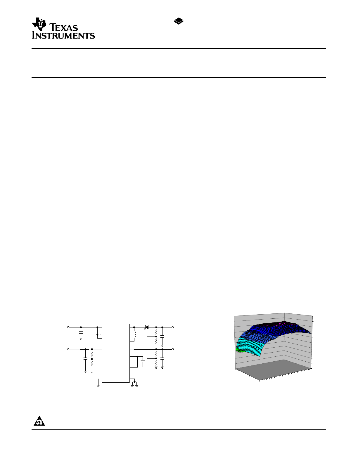
DESCRIPTION
The TPS6512x DC-DC converter supplies all three voltages required by amorphous-silicon (a-Si) and
low-temperature poly-silicon (LTPS) TFT-LCD displays. The compact layout of the TPS6512x uses a single
inductor to generate independently-regulated positive and negative outputs. A free-running variable peak current
PWM control scheme time-multiplexes the inductor between outputs. This control architecture operates at a
pseudo-fixed-frequency to provide fast response to line and load transients while maintaining a relatively
constant switching frequency and high efficiency over a wide range of input and output voltages. Due to the high
switching frequency capability of the device, inexpensive and ultra-thin 8.2 or 10 µH inductors can be used.
The main output, V
auxiliary outputs generate a boosted output voltage, V
-18 V for the LCD gate drive. The device has internal current limiting for high reliability under fault conditions.
Additionally, the device offers a fixed output linear regulator for the LCD logic circuitry.
, is post-regulated to provide a low-ripple source drive voltage for the LCD display. The
MAIN
, up to 20 V, and a negative output voltage, V
GH
GL
, down to
Please be aware that an important notice concerning availability, standard warranty, and use in critical applications of Texas
Instruments semiconductor products and disclaimers thereto appears at the end of this data sheet.
PRODUCTION DATA information is current as of publication date.
Products conform to specifications per the terms of the Texas
Instruments standard warranty. Production processing does not
necessarily include testing of all parameters.
Figure 1. Typical Application Figure 2. Core Converter Efficiency
Copyright © 2004–2005, Texas Instruments Incorporated
www.ti.com
TPS65120, TPS65121, TPS65123, TPS65124
SLVS531A – JUNE 2004 – REVISED MARCH 2005
These devices have limited built-in ESD protection. The leads should be shorted together or the device
placed in conductive foam during storage or handling to prevent electrostatic damage to the MOS gates.
ORDERING INFORMATION
T
A
-40 to 85°C
(1) The xyz package is available in tape and reel. Add R suffix (xyzR) to order quantities of TBD parts. Add T suffix (xyzT) to order
quantities of 250 parts.
INTEGRATED POWER SEQUENCING PACKAGE PART NUMBER
LINEAR REGULATOR MARKING
Fixed 3.3V output voltage Automatic Power-Up/Down 3 × 3 QFN-16 TPS65120RGT BKA
Fixed 1.8V output voltage Automatic Power-Up/Down 3 × 3 QFN-16 TPS65121RGT BKB
NO Automatic Power-Up/Down 3 × 3 QFN-16 TPS65123RGT BKC
NO Programmable 3 × 3 QFN-16 TPS65124RGT BKD
Power-Up/Down
ABSOLUTE MAXIMUM RATINGS
over operating free-air temperature range (unless otherwise noted)
VIN -0.3 V to +6 V
Input voltage
Voltage
Input voltage at GATE, EN, RUN
Power dissipation Internally limited
Operating temperature range -40°C to 85°C
Maximum operating junction temperature, TJ(max) 135°C
Storage temperature range 65°C to 150°C
(1) Stresses beyond those listed under "absolute maximum ratings" may cause permanent damage to the device. These are stress ratings
only and functional operation of the device at these or any other conditions beyond those indicated under "recommended operating
conditions" is not implied. Exposure to absolute-maximum-rated conditions for extended periods may affect device reliability.
(2) All voltage values are with respect to network ground terminal.
(2)
(2)
SWN VIN- 24 V to VIN+0.3 V
SWP - 0.3 V to +23 V
VGH - 0.3 V to +21 V
VMAIN, LDOIN, LDOOUT, ENVGL, ENVGH - 0.3 V to +6 V
BOOT - 0.3 V to +6.2 V
(2)
(1)
(1)
UNIT
-0.3 V to VIN+ 0.3 V
PACKAGE
DISSIPATION RATINGS
PACKAGE R
RGT 68°C/W 15mW/°C
(1) Maximum power dissipation is a function of TJ(max), θJAand TA. The maximum allowable power
dissipation at any allowable ambient temperature is PD= [TJ(max)-T
2
θ JA
DERATING FACTOR ABOVE TA= 25°C
(1)
]/ θJA.
A
www.ti.com
TPS65120, TPS65121, TPS65123, TPS65124
SLVS531A – JUNE 2004 – REVISED MARCH 2005
ELECTRICAL CHARACTERISTICS
V
= 3.6 V, EN = RUN = VIN, L = 10 µH, TA= -40°C to 85°C, typical values are at TA= 25°C (unless otherwise noted)
IN
PARAMETER TEST CONDITIONS MIN TYP MAX UNIT
CONVERTER STAGE
R
≥ 330 Ω at V
L_MAIN
R
≥ 12 k Ω at V
Input voltage for full load operation 2.7 5.5 V
V
IN
Minimum input voltage for start-up 2.5 V
f Switching frequency 4.0 MHz
P
GH
P
GL
Output power on V
Output power on V
GH
GL
L_VGH
R
≥ 12 k Ω at V
L_VGL
V
= GND, TA= -40°C to 85°C
LDOIN
R
≥ 660 Ω at V
L_MAIN
R
≥ 24 k Ω at V
L_VGH
R
≥ 24 k Ω at V
L_VGL
V
= GND, TA= -20°C to 85°C
LDOIN
R
= 250 Ω at V
L_MAIN
V
= ENVGH = ENVGL = GND
LDOIN
VIN≥ 2.7 V 35
VIN≥ 2.5 V 15
VIN≥ 2.7 V 35
VIN≥ 2.5 V 15
VIN≥ 2.5 V 60
P
TOT
Total output power on
V
+ V
BOOT
+ V
GH
GL
VIN≥ 2.7 V 120
VIN≥ 3 V 150
VIN≥ 4.5 V 250
η Power efficiency V
I
LIM
I
START-UP
P-MOS1 current limit 2.7 V ≤ VIN≤ 5.5 V 150 200 mA
P-MOS1 start-up current limit 2.7 V ≤ VIN≤ 5.5 V 65 mA
P-MOS1 switch on-resistance Ω
r
DS(ON)
N-MOS1 switch on-resistance Ω
P-MOS1 leakage current 0.01
N-MOS1 leakage current 0.01
N-MOS2 + P-MOS2 forward voltage drop 400 600 mV
N-MOS3 + D1 forward voltage drop 900 1100 mV
MAIN
= 15 V, V
GH
IGH= IGL= 100 µA, V
VIN= V
VIN= V
V
= V
BOOT
V
= V
BOOT
V
= 6 V, TA= 25°C µA
DS
V
= V
GS
I
= ID= 50 mA
BOOT
V
= V
GS
IGH= ID= 50 mA
BOOT
GL
= 3.6 V 2.5 4.3
GS
= 2.5 V 3.8 6.9
GS
= 3.7 V 1.9 3.5
GS
= 5 V 1.4 2.3
GS
= 5.5 V, V
BOOT
= 5.5 V, V
BOOT
V
= 5.0 V, I
CONVERTER SUPPLY CURRENT
Quiescent current into VIN I
Quiescent current into BOOT 30 60
I
Q
Quiescent current into VGH 0.1 1
I
SD
Shutdown current TA= 25°C 0.1 1 µA
= IGH= IGL= 0 mA, 140 170
MAIN
V
= +15 V, V
GH
V
MAIN
V
FBL
V
LDOIN
TA= 25°C
= 5 V, V
= -0.2 V, V
GL
FBH
= GND, EN = RUN = VIN,
BOOT
= 5 V,
MAIN
= 12 V,
GH
= -12 V,
GL
= 5 V,
MAIN
= 12 V,
GH
= -12 V,
GL
= 5 V
MAIN
= 20 mA,
= -10 V, 83%
= GND
LDOIN
= 2 V,
SWP
= 2 V,
SWP
= -15 V,
= V
= +1.5 V,
FBM
= 5.25 V,
mW
mW
mW
µA
3
www.ti.com
TPS65120, TPS65121, TPS65123, TPS65124
SLVS531A – JUNE 2004 – REVISED MARCH 2005
ELECTRICAL CHARACTERISTICS (continued)
V
= 3.6 V, EN = RUN = VIN, L = 10 µH, TA= -40°C to 85°C, typical values are at TA= 25°C (unless otherwise noted)
IN
PARAMETER TEST CONDITIONS MIN TYP MAX UNIT
MAIN OUTPUT
V
MAIN
I
MAIN
V
FBM
I
FBM
I
SC_MAIN
R
DIS_VMAIN
VGH OUTPUT
V
GH
I
GH
V
FBH
I
FBH
R
DIS_VGH
VGL OUTPUT
V
GL
I
GL
V
FBL
I
FBL
Main output voltage range 3.0 5.6 V
V
≤ 5.3 V 25
Maximum main output current mA
Feedback regulation voltage
Feedback input bias current V
Load regulation I
Minimum dropout voltage I
Main output voltage ripple I
Short-circuit current limit V
MAIN
V
≥ 5.3 V 7.5
MAIN
2.7 V ≤ VIN≤ 5.5 V, 100 µA ≤ I
TA= -20°C to 50°C
≤ 25 mA,
MAIN
2.7 V ≤ VIN≤ 5.5 V,
0 mA ≤ I
FBM
MAIN
MAIN
MAIN
BOOT
≤ 25 mA
MAIN
= V
REF
= 0 to 25 mA, V
= 5 V 0.006 %/mA
MAIN
= 10 mA 130 mV
= 10 mA 5 mV
= 5.5 V 50 mA
Discharge resistor for power-down sequence
V
output voltage range VIN+ 0.5 20 V
GH
Maximum DC output current 6 mA
V
precharge resistor 1 k Ω
GH
Feedback regulation voltage 2.7 V ≤ VIN≤ 5.5 V, 0 mA ≤ IGH≤ 2 mA 1.177 1.213 1.249 V
Feedback input bias current V
Load regulation IGH= 0 to 2 mA, V
= 0 V 0.01 0.1 µA
FBH
= 15 V -0.11 %/mA
GH
Line regulation VIN= 2.7 V to 5.5 V, IGH= 100 µA 0.01 %/V
V
output voltage ripple 20 mV
GH
200 µA load, V
C
= 220 nF, C
OUT
= 15 V,
GH
= 10 pF
FF
Discharge resistor for power-down sequence
V
Output voltage range -18 -2.5 V
GL
Maximum DC output current 6 mA
Feedback regulation voltage 2.7 V ≤ VIN≤ 5.5 V, 0 mA ≤ IGL≤ 2 mA -0.036 0 0.036 V
Feedback input bias current V
Load regulation IGL= 0 to 2 mA, V
= 0 V 0.01 0.1 µA
FBL
= -15 V 0.13 %/mA
GL
Line regulation VIN= 2.7 V to 5.5 V, IGL= 100 µA 0.1 %/V
V
output voltage ripple 20 mV
GL
200 µA load, V
C
= 220 nF
OUT
= -15 V,
GL
1.203 1.213 1.223 V
1.195 1.213 1.231 V
0.01 0.1 µA
P-P
10 k Ω
10 k Ω
4
www.ti.com
TPS65120, TPS65121, TPS65123, TPS65124
SLVS531A – JUNE 2004 – REVISED MARCH 2005
ELECTRICAL CHARACTERISTICS (continued)
V
= 3.6 V, EN = RUN = VIN, L = 10 µH, TA= -40°C to 85°C, typical values are at TA= 25°C (unless otherwise noted)
IN
PARAMETER TEST CONDITIONS MIN TYP MAX UNIT
LINEAR REGULATOR STAGE - AUXILIARY OUTPUT
V
LDOIN
V
LDOOUT
I
LDOOUT
I
SC_LDO
I
Q_LDO
I
SD_LDO
GATE DRIVER
V
IH
V
IL
UNDERVOLTAGE LOCKOUT
V
UVLO
LOGIC SIGNALS EN, RUN, ENVGL, ENVGH
V
IH
V
IL
I
LKG
Input voltage range 2.5 5.8 V
Output voltage range 1.8 V
Maximum output current 20 mA
Short-circuit current limit V
Minimum dropout voltage I
Total accuracy ±3%
Load regulation I
Line regulation 0.013 %/V
Linear regulator quiescent current 11 20 µA
LDOOUT
2.5 V ≤ V
0 mA ≤ I
LDOOUT
V
to 5.5 V, I
V
TA= 25°C
= 0 V 50 mA
LDOOUT
= 10 mA 400 mV
≤ 5.5 V,
LDOIN
≤ 20 mA
LDOOUT
= 0 to 20 mA 0.006 %/mA
= V
LDOIN
LDOOUT
= V
LDOIN
LDOOUT
LDOOUT
+ 0.5 V (min 2.5 V)
= 20 mA
+ 0.4 V (min 2.5 V),
Linear regulator shutdown current GATE = VIN 0.2 1 µA
Gate output pull-down resistance V
< 500 mV 100 k Ω
GATE
Gate output pull-up resistance 100 k Ω
High level input voltage 1.4 V
Low level input voltage 0.4 V
Undervoltage lockout threshold VINfalling 2.15 2.3 V
High level input voltage 1.4 V
Low level input voltage 0.4 V
Logic input leakage current µA
ENVGL, ENVGH = VINor GND (TPS65124) 0.01 0.1
EN, RUN = V
IN
EN, RUN pin pull-down resistance EN, RUN ≤ 0.4 v 100 k Ω
0.01 0.1
V
LDOIN
-0.5
5
www.ti.com
1
2
3
4
12
11
10
9
5 6 7 8
131516
EN
RUN
ENVGL
ENVGH
FBL
FBM
AGND
VMAIN
PGND
BOOT
VGH
FBH
GATE
VIN
SWN
SWP
1
2
3
4
12
11
10
9
5 6
7
8
13141516
EN
RUN
AGND
AGND
FBL
FBM
AGND
VMAIN
PGND
BOOT
VGH
FBH
GATE
VIN
SWP
1
2
3
4
12
11
10
9
5 6
7
8
13141516
Exposed
Thermal Die*
EN
RUN
LDOIN
LDOOUT
FBL
FBM
AGND
VMAIN
PGND
BOOT
VGH
FBH
GATE
VIN
SWN
SWP
AGND
SWN
Exposed
Thermal Die*
AGND
14
Exposed
Thermal Die*
AGND
TPS65120/1/2
(TOP VIEW)
TPS65123
(TOP VIEW)
TPS65124
(TOP VIEW)
TPS65120, TPS65121, TPS65123, TPS65124
SLVS531A – JUNE 2004 – REVISED MARCH 2005
PIN ASSIGNMENTS
TERMINAL FUNCTIONS
TERMINAL
NAME NO.
VIN 15 I This is the input voltage pin of the device.
GATE 16 I/O section), or an active high control input. Pulling GATE above the 1.4 V logic-high level and RUN to a logic-low
RUN 2 I
EN 1 I floating. A simultaneous logic-high level on EN and RUN enables the converter and a logic-low shuts down
SWN 14 I/O Connect the inductor to this pin. This pin is connected to the source of the high-side MOSFET switch.
SWP 13 I/O Connect the inductor to this pin. This pin is connected to the drain of the low-side MOSFET switch.
PGND 12 O Power ground. Connect to AGND underneath the IC.
VGH 10 O Positive output
BOOT 11 O
VMAIN 8 I Main output
FBH 9 I Feedback pin for the positive output voltage divider. Regulates to 1.213 V nominal.
FBL 5 I
FBM 6 I Feedback pin for the main output voltage divider. Regulates to 1.213V nominal.
AGND 7, 3, 4
LDOIN 3 I (TPS65120/1/2). The low-dropout series-pass regulator (LDO) is enabled according to the GATE signal
LDOOUT 4 O Auxiliary linear regulator output (TPS65120/1/2).
ENVGL 3 I Enable pin for negative output (TPS65124). This pin should be terminated and not be left floating.
ENVGH 4 I Enable pin for positive output (TPS65124). This pin should be terminated and not be left floating.
I/O DESCRIPTION
This pin can either be the gate driver output to an external small P-Channel MOSFET (see application
level disables the integrated active power-down sequencing.
RUN controls the external P-Channel MOSFET. This pin must be terminated and not be left floating. Forcing
this pin to a logic-high level turns on the external MOSFET switch.
This is the enable pin of the multiple-output dc-to-dc converter. This pin must be terminated and not be left
the device.
Provides a bootstrapped supply for the rectifier MOSFET driver, enabling the gate of the MOSFET to be
driven above the output voltage.
Feedback pin for the negative output voltage divider. Regulates to 0 V nominal. Connect feedback resistor
divider between VGL and main output.
Analog ground. Connect to power ground (PGND) underneath IC. Pins 3 and 4 are only used for AGND in
TPS65123.
Auxiliary linear regulator input. If this pin is connected to GND, the voltage regulator is disabled
timing.
6
www.ti.com
Current Limit
Comparator
Undervoltage
Lockout
Bias Supply
VIN
SWP
LDOOUT
SWN
T
on
VGH
BOOT
PGND
VMAINLDO
BOOT
V
REF
R
V
REF
R
FBH
R
FBL
BOOT
FBM
AGND
Bandgap
V
REF
= 1.213V
Power Up/Down
Sequencer
Oscillator
S
Min Off Time
VMAIN
Control
Logic
EN
BOOT
BOOT
P−MOS1
P−MOS2
N−MOS1
N−MOS2
N−MOS3
D1
RUN
VMAIN
GATE
EN
100kR
Power Down Seq Off
Power Down Seq Off
R
DIS_VGH
R
DIS_VMAIN
EN
LDO
LDOIN
EN_LDOAUX
NOT PRESENT IN TPS65123
FUNCTIONAL BLOCK DIAGRAM - TPS65120/1/2/3
TPS65120, TPS65121, TPS65123, TPS65124
SLVS531A – JUNE 2004 – REVISED MARCH 2005
7
www.ti.com
Current Limit
Comparator
Undervoltage
Lockout
Bias Supply
VIN
SWP
SWN
T
on
VGH
BOOT
PGND
VMAIN
BOOT
V
REF
R
V
REF
R
FBH
R
FBL
BOOT
FBM
AGND
Power Up/Down
Sequencer
Oscillator
S Min Off Time
VMAIN
Control
Logic
EN
BOOT
BOOT
P−MOS1
P−MOS2
N−MOS1
N−MOS2
N−MOS3
D1
RUN
VMAIN
GATE
EN
100kR
Power Down Seq Off
Power Down Seq Off
R
DIS_VGH
R
DIS_VMAIN
EN
ENVGH
ENVGL
Bandgap
V
REF
= 1.213V
LDO
TPS65120, TPS65121, TPS65123, TPS65124
SLVS531A – JUNE 2004 – REVISED MARCH 2005
FUNCTIONAL BLOCK DIAGRAM - TPS65124
8
www.ti.com
PARAMETER MEASUREMENT INFORMATION
SWN
TPS65120
D1
L1
10
C1
F
V
IN
2.7 V to 5.5 V
V
GL
down to −18 V/2 mA
C3
220 nF
R4
R3
SWP
FBL
VMAIN
FBM
C5
220 nF
R6
R5
V
MAIN
3.0 V to 5.3 V/20 mA
C4
1
BOOT
VGH
C2
220 nF
V
GH
up to 20 V/2 mA
PGND
AGND
FBH
RUN
V
AUX
3.3 V/20 mA
EN
VIN
A
A
GATE
LDOIN
LDOOUT
C6
220 nF
R2
R1
List of Components:
U1 = TPS6512x
L1 = EPCOS SIMID1812-C
D1 = ZETEX ZUMD54C
CX = X5R/X7R
2.2 FH
TPS65120, TPS65121, TPS65123, TPS65124
SLVS531A – JUNE 2004 – REVISED MARCH 2005
η Core converter efficiency vs Load current 3
V
MAIN
V
, V
GH
V
GH
V
GL
f
s
I
Q
TYPICAL CHARACTERISTICS
Table of Graphs
FIGURE
vs Input voltage 4
Main output efficiency vs Load current 5
vs Input voltage 6
Output ripple voltage 7
DC output voltage vs Load current 8
Load transient response 9
GL
Positive, negative output ripple voltage 10, 11
DC output voltage vs Load current 12
DC output voltage vs Load current 13
Switching frequency vs Load current 14
No load quiescent current vs Input voltage 15
Power-Up Sequencing (TPS65120) 16
Power-Down Sequencing (TPS65120) 17
9

www.ti.com
60
65
70
75
80
85
90
95
100
2.7 3.1 3.5 3.9 4.3 4.7 5.1 5.5
I
BOOT
= 15 mA
I
BOOT
= 5 mA
VIN = 3.6 V ,
V
MAIN
= 5 V,
ENVGL = ENVGH = GND
VIN − Input Voltage − V
Core Converter Efficiency − %
0
10
20
30
40
50
60
70
80
90
100
0.1 1 10 100
Core Converter Efficiency − %
I
BOOT
− Output Current − mA
VIN = 3.6 V
ENVGL = ENVGH = GND
V
MAIN
= 5 V
30
40
50
60
70
80
90
100
0 2 4 6 8 10 12 14 16 18 20
I
MAIN
− Output Current − mA
Main Output Efficiency − %
V
MAIN
= 5 V ,
VGH = 15 V @ 200 A,
VGL = −10 V @ 200 A
V
MAIN
= 3.3 V ,
VGH = 7.5 V @ 200 A,
VGL = −3 V @ 200 A
VIN = 3.6 V
40
45
50
55
60
65
70
75
80
85
90
95
100
2.7 3.1 3.5 3.9 4.3 4.7 5.1 5.5
V
MAIN
= 5 V @ 10 mA,
VGH = 15 V @ 200 A,
VGL = −10 V @ 200 A
V
MAIN
= 5 V @ 5 mA,
VGH = 15 V @ 200 A,
VGL = −10 V @ 200 A
V
MAIN
= 3.3 V @ 10 mA,
VGH = 7.5 V @ 200 A,
VGL = −3 V @ 200 A
VIN − Input Voltage − V
Main Output Efficiency − %
TPS65120, TPS65121, TPS65123, TPS65124
SLVS531A – JUNE 2004 – REVISED MARCH 2005
CORE CONVERTER EFFICIENCY CORE CONVERTER EFFICIENCY
TPS65124 TPS65124
vs vs
LOAD CURRENT INPUT VOLTAGE
Figure 3. Figure 4.
MAIN OUTPUT EFFICIENCY MAIN OUTPUT EFFICIENCY
vs vs
LOAD CURRENT INPUT VOLTAGE
10
Figure 5. Figure 6.

www.ti.com
V
BOOT
(50 mV/div,
5.8 V Offset)
V
MAIN
(10 mV/div,
5 V Offset)
V
IN
= 3.6 V ,
V
MAIN
= 5 V @ 20 mA,
ENVGL = ENVGH = LOW
t − Time − 5 s/div
4.95
4.96
4.97
4.98
4.99
5
5.01
5.02
5.03
5.04
5.05
0 2 4 6 8 10 12 14 16 18 20
I
MAIN
− Output Current − mA
VIN = 3.6 V ,
VGH = 15 V @ 200 A,
VGL = −10 V @ 200 A
V − Output Voltage − V
MAIN
V
GH
(50 mV/div,
AC Coupled)
V
GL
(20 mV/div,
AC Coupled)
V
IN
= 3.6 V ,
V
MAIN
= 5 V @ 5 mA,
VGH = 15 V @ 100 A,
VGL = −10 V @ 100 A
t − Time − 20 s/div
V
MAIN
(50 mV/div,
5 V Offset)
I
MAIN
(10 mA/div)
t − Time − 10 s/div
V
IN
= 3.6 V ,
V
MAIN
= 5 V ,
ENVGL = ENVGH = LOW
C
OUT
= 220 nF
TPS65120, TPS65121, TPS65123, TPS65124
SLVS531A – JUNE 2004 – REVISED MARCH 2005
MAIN DC OUTPUT VOLTAGE
MAIN OUTPUT RIPPLE VOLTAGE LOAD CURRENT
Figure 7. Figure 8.
MAIN OUTPUT LOAD
TRANSIENT RESPONSE POSITIVE, NEGATIVE OUTPUT RIPPLE
vs
Figure 9. Figure 10.
11

www.ti.com
V
GH
(20 mV/div,
AC Coupled)
V
GL
(20 mV/div,
AC Coupled)
t − Time − 10 s/div
V
IN
= 3.6 V ,
V
MAIN
= 5 V @ 5 mA,
VGH = 15 V @ 100 A,
VGL = −10 V @ 100 A
10 pF Feed-Forward
Capacitor Across R
1
14.85
14.90
14.95
15
15.05
15.10
15.15
0.1 1 10
IGH − Output Current − mA
V
GH
− DC Output Voltage − V
VIN = 3.6 V ,
V
MAIN
= 5 V, @ 5 mA
VGL = −10 V @ 200 A
−10.10
−10.08
−10.06
−10.04
−10.02
−10
−9.98
−9.96
−9.94
−9.92
−9.90
0.1
1
10
VIN = 3.6 V ,
V
MAIN
= 5 V @ 5 mA,
VGH = 15 V @ 200 A
IGL − Output Current − mA
V
GL
− DC Output Voltage − V
1
10
0.1 1 10 100
VIN = 3.6 V ,
V
MAIN
= 5 V ,
ENVGH = ENVGL = GND
Switching Frequency − MHz
I
MAIN
− Output Current − mA
TPS65120, TPS65121, TPS65123, TPS65124
SLVS531A – JUNE 2004 – REVISED MARCH 2005
POSITIVE, NEGATIVE OUTPUT
RIPPLE VOLTAGE POSITIVE OUTPUT (VGH) LOAD REGULATION
Figure 11. Figure 12.
NEGATIVE OUTPUT (VGL) LOAD REGULATION LOAD CURRENT
SWITCHING FREQUENCY
Figure 13. Figure 14.
vs
12

www.ti.com
V
LOGIC
V
MAIN
V
GH
V
GL
VIN = 3.6 V , EN = HIGH,
R
MAIN
= 1 k,
RGH = 120 k,
RGL = 100 k,
RUN
V
LOGIC
(5 V/div)
V
MAIN
(2 V/div)
V
GH
(5 V/div)
V
GL
(5 V/div)
t − Time − 100 s/div
0
50
100
150
200
250
300
2.5 2.8 3 3.3 3.5 3.8 4 4.3 4.5 4.8 5 5.3 5.5
V
MAIN
= 3.3 V , VGH = 7.5 V , VGL = −3 V
No-Load Quiescent Current Includes
Output Voltage Divider Network Bias Current
I
Q
− Quiescent Current − I
Q
A
VIN − Input Voltage − V
V
LOGIC
V
MAIN
V
GH
V
GL
VIN = 3.6 V, EN = HIGH,
R
MAIN
= 1 k,
RGH = 120 k,
RGL = 100 k,
RUN
V
MAIN
(2 V/div)
V
GH
(5 V/div)
V
GL
(5 V/div)
t − Time − 5 ms/div
V
LOGIC
(5 V/div)
TPS65120, TPS65121, TPS65123, TPS65124
SLVS531A – JUNE 2004 – REVISED MARCH 2005
QUIESCENT CURRENT
vs TPS65120
INPUT VOLTAGE POWER-UP SEQUENCING
Figure 15. Figure 16.
TPS65120
POWER-DOWN SEQUENCING
Figure 17.
13

www.ti.com
TPS65120, TPS65121, TPS65123, TPS65124
SLVS531A – JUNE 2004 – REVISED MARCH 2005
DETAILED DESCRIPTION
The standard application circuit ( Figure 1 ) of the TPS65120 is a complete power supply for TFT LCD displays.
The circuit generates four independent supplies for the source driver (V
logic supply for the timing controller. The input voltage range is from 2.5 V to 5.5 V.
The TPS65120/1/2 contains a high-performance switching regulator and two low-dropout linear regulators
(LDOs). One of the LDOs generates V
and the other powers the logic inside the panel. The TPS65123
MAIN
includes only one linear regulator to provide the main output with low ripple voltage and can be set from 3.0 V to
5.3 V with an external resistor voltage divider. The TPS65124 integrates programmable power sequencing for
highest flexibility.
OPERATION
The TPS6512x generates both positive and negative supply voltages using a single inductor. It alternates
between acting as a step-up converter and an inverting converter on a cycle-by-cycle basis. All output voltages
are independently regulated.
A free-running, variable-peak-current PWM control scheme is used to time-multiplex the inductor between BOOT,
V
, and V
GH
fast response to line and load transients while maintaining a relatively constant switching frequency and high
efficiency over a wide range of input and output voltages.
During the first cycle of operation, internal switches N-MOS1 and P-MOS1 are turned on. SWN connects to VIN,
SWP pulls to ground and the inductor current rises. Once the inductor current reaches the DC current limit (I
of 150 mA (typ) the internal control logic can either turn off N-MOS1 or P-MOS1 to service the requesting output.
Depending on the required output power, the converter starts another cycle or enters a pulse-skipping
modulation scheme to increase efficiency under light loads. The current into the SWN pin measures the inductor
current. The TPS6512x controls the inductor current to regulate BOOT, V
To achieve low ripple voltage and high accuracy, the main output (V
This LDO regulator regulates energy from the BOOT output down to 5.3 V (max). To achieve the highest
efficiency, the BOOT voltage is regulated to minimize the dropout voltage across the LDO to approximately V
+ 0.5 V.
In addition, the VMAIN, VGH, VGL outputs are monitored for fault conditions that last longer than the fault-timer
period of 100 µs (typ). The device goes into a latched shutdown state in case of a fault condition.
outputs. This inherently-stable control architecture operates at a pseudo fixed frequency, providing
GL
MAIN
), the gate drivers (V
MAIN
, and V
GH
GL
output voltages.
, V
GH
) is post-regulated by an integrated LDO.
GL
) and a
)
LIM
MAIN
Soft Start
The TPS6512x has an internal soft-start circuit that limits the inrush current during startup. This prevents possible
voltage drops of the input voltage in case the battery or a high impedance power source is connected to the input
of the device.
The device powers up by precharging the BOOT output capacitor to VIN. During the precharge phase, the
current through the rectifying switch N-MOS2 is limited. This also limits the output current under short-circuit
conditions on the BOOT output. To ensure proper startup of the device, the BOOT output must be left unloaded
during the precharge phase.
After the precharge phase, the converter operates with an I
START-UP
current limit of 65 mA (typ), then increases
gradually to the full current limit of 150 mA (typ).
Undervoltage Lockout
To ensure that the input voltage is high enough for reliable operation, the TPS6512x includes an under-voltage
lockout (UVLO) circuit. The UVLO threshold at the VIN pin is 2.15 V (typ) falling and 2.25 V (typ) rising. The 100
mV (typ) hysteresis prevents supply transients from causing restarts.
Once the input voltage exceeds the UVLO rising threshold, the controller can enable the reference voltage and
precharges BOOT. When the input voltage falls below the UVLO falling threshold, the controller turns off the
reference and all the regulator outputs, and pulls GATE high with an internal 100 k Ω resistor to turn off P1 (
Figure 18 ).
14

www.ti.com
SWN
TPS65120
D1
L1C1
C3
R4
R3
SWP
FBL
VMAIN
FBM
C5
R6
R5
C4
BOOT
VGH
C2
FBH
RUN
EN
VIN
GATE
R10
R9
C7
P1
PGND
AGND
A A
LDOIN
LDOOUT
VIN = 3.3 V
V
GH
V
LOGIC
= 3.3 V
V
GL
V
MAIN
R1
R2
V
IN
RUN
V
LOGIC
, EN
V
MAIN
V
GL
V
GH
V
BOOT
5.75V
GATE, EN_LDOAUX
TPS65120, TPS65121, TPS65123, TPS65124
SLVS531A – JUNE 2004 – REVISED MARCH 2005
DETAILED DESCRIPTION (continued)
Enable and Power Sequencing (TPS65120/1/2/3)
To correctly power up most TFT panels, the gate-drive supplies must be sequenced such that the negative
supply (V
enable pin.
Once RUN is high, the TPS65120/1/2/3 turns on the external P-channel MOSFET P1 (see Figure 18 ) by pulling
GATE low. GATE is pulled down with a 100 k Ω resistor. The DC/DC converter then starts, enabling the BOOT
output.
Pulling the enable pin (EN) high enables the MAIN output. When the output voltage V
nominal value, the negative output enables. V
nominal value.
Pulling the RUN pin low shuts down the device. Power-down sequencing starts by switching off V
The V
feedback voltage divider. The required time to discharge the output capacitor at V
current. Once V
This sequence is shown in Figure 19 .
When no power sequencing is required on the digital supply voltage (V
and GATE can be connected to a logic-high level to disable the power-down sequencer. Each output turns off
depending upon load current and output capacitance.
) powers up before the positive supply (V
GL
GH
output capacitor is actively discharged by an internal resistor while V
GH
has reached 1.2 V (typ) the main output is turned off followed by the output voltage V
FBL
). The TPS65120/1/2/3 controls this sequence through an
GH
is delayed until the negative voltage has reached 90% of its
GL
GL
), tie EN and RUN signals together
LOGIC
has reached 90% of its
MAIN
and V
GH
is only discharged by its
output depends on the load
GL
.
.
LOGIC
Figure 18. Power Sequencing on Digital Supply Voltage, Figure 19. TPS65120/1/2/3 Power Sequence
V
LOGIC
15

www.ti.com
SWN
TPS65124
D1
L1
C1
VIN = 3.3V
V
GL
C3
R4
R3
SWP
FBL
VMAIN
FBM
C5
R6
R5
V
MAIN
C4
BOOT
VGH
C2
V
GH
FBH
RUN
GATE
VIN
EN
V
LOGIC
= 3.3V
P1
PGND
AGND
A
A
ENVGH
ENVGL
ENVGH
ENVGL
EN
D2
optional
R1
R2
V
LOGIC
V
IN
RUN
GATE
V
MAIN
V
GL
V
GH
V
BOOT
5.75V
ENVGH
ENVGL
EN
TPS65120, TPS65121, TPS65123, TPS65124
SLVS531A – JUNE 2004 – REVISED MARCH 2005
DETAILED DESCRIPTION (continued)
Enable and Power Sequencing (TPS65124)
The TPS65124 controls the power sequencing of V
These pins must be terminated and not be left floating to prevent instability.
Once RUN is pulled high and the input voltage on VIN exceeds the rising input UVLO threshold, the reference is
turned on and the external P-channel MOSFET P1 (see Figure 20 ) is switched on by pulling GATE low. The
GATE is pulled down with a 100 k Ω resistor. The DC/DC converter then starts up, enabling the BOOT output.
Pulling enable pin high (EN) powers on the MAIN output. This power sequencing must occur before the gate
voltages are enabled. Conversely V
and V
GL
output voltages must be turned off by pulling ENVGL and ENVGH
GH
inputs to ground before the MAIN output is switch off.
To clamp the V
output near zero when the MAIN output is still on, an external diode (D2) can be used. In some
GL
applications this diode may already be implemented in the display.
, V
LOGIC
, V
MAIN
and V
GH
with four separate enable pins.
GL
Figure 20. Power Sequencing on Digital Supply Voltage, Figure 21. TPS65124 Programmable Power Sequence
V
LOGIC
Fault Protection
All TPS6512x outputs are protected against a short circuit to ground. During steady-state operation, if the output
V
, V
MAIN
Once V
or V
GH
comes down to 700 mV typ, the GATE output is pulled to V
MAIN
falls below its fault detection threshold the device simultaneously turns off all three outputs.
GL
, the auxiliary LDO (TPS65120/1/2) is
IN
disabled and the device enters a shutdown state.
The auxiliary LDO present in TPS65120/1/2 has an integrated current foldback circuit for reliable short-circuit
protection.
The device can be enabled again by toggling the enable pins (RUN, EN) below 0.4 V or by cycling the input
voltage below the UVLO falling threshold (2.15 V typ).
16

www.ti.com
GHGHGH
IVP ×=
GLGLGL
IVP ×=
5.0VVforI
0.5V
V
PP
MAININMAIN
MAIN
MAIN
MAIN_LDOMAINBOOT
2
+<×
+
≈η×=
MAININMAIN
IN
MAIN
MAIN_LDOMAINBOOT
VVforI
V
V
PP
2
>×≈η×=
FBMMAIN
R6
R6R5VV+
×=
FBHGH
R2
R2R1VV+
×=
MAINGL
R4
R3
VV ×=
TPS65120, TPS65121, TPS65123, TPS65124
SLVS531A – JUNE 2004 – REVISED MARCH 2005
APPLICATION INFORMATION
OUTPUT POWER CAPABILITY
The first step in the design procedure is to calculate the maximum output current for each output under certain
input and output voltage conditions. The TPS6512x uses time-multiplex operation to share the inductive storage
element between BOOT, VGH and VGL outputs. To avoid complex calculations it is recommended to use the
specified output-power data from the electrical characteristics table to determine the maximum output-power
capability.
The following example shows how to proceed for given requirements:
• Input Voltage = 3.0 V
• MAIN Output = 5.0 V @ 10 mA
• VGH output = 12 V @ 500 µA
• VGL output = -12 V @ 300 µA
1. Calculate Maximum Output Power on VGH Output
2. Calculate Maximum Output Power on VGL Output
3. Calculate Maximum Output Power on BOOT Output
4. Maximum Output Power Verification
The electrical characteristics table states that for V
must be lower than 35 mW each. Furthermore, the total output power (P
> 3.0 V, the maximum power on VGH and VGL outputs
IN
+ P
BOOT
+ P
GH
GL
) must be lower than
150 mW.
In our design example, P
GH
= 6 mW, P
= 3.6 mW, and P
GL
= 55 mW. Since these numbers are well below
BOOT
the specified values, we can conclude that TPS6512x can reasonably power such a display.
SETTING THE OUTPUT VOLTAGE
The output voltages are defined as shown in Figure 22 .
with an internal reference voltage V
with an internal reference voltage V
To minimize the operating quiescent current, set R2, R4 and R6 in the range 100 k Ω to 300 k Ω . Great care
should be taken to route the FBx lines away from noise sources such as the inductor or the SWN and SWP lines.
A feed-forward capacitor across the upper feedback resistor (R1, R3) on VGH and VGL outputs can be used to
provide more overdrive for the error comparator. This feed-forward capacitor helps to reduce the output ripple
voltage. A good starting value is 10 pF.
typical = 1.213V.
FBM
typical = 1.213V.
FBH
17

www.ti.com
SWN
TPS65120
D1
L1
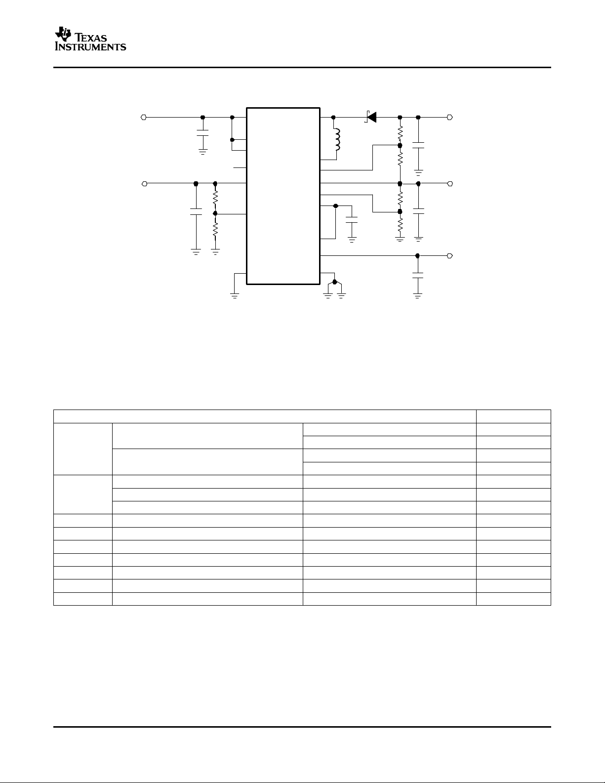
10
C1
2.2
V
IN
2.7 V to 5.5 V
V
GL
down to −18 V/2 mA
C3
100 nF
R4
R3
SWP
FBL
VMAIN
FBM
C5
220 nF
R6
R5
V
MAIN
3.0 V to 5.3 V/25 mA
C4
1
BOOT
VGH
C2
100 nF
V
GH
up to 20 V/2 mA
PGND
AGND
FBH
RUN
V
AUX
3.3 V/20 mA
EN
VIN
A
A
GATE
LDOIN
LDOOUT
C6
220 nF
R1
R2
µF
µF
Hµ
TPS65120, TPS65121, TPS65123, TPS65124
SLVS531A – JUNE 2004 – REVISED MARCH 2005
APPLICATION INFORMATION (continued)
The larger the feed-forward capacitor the worse the load regulation of the device. Therefore, when concern for
load regulation is paramount, select a capacitor value as small as possible. Another possibility to further reduce
ripple voltage on VGH and VGL outputs is to increase output-capacitor values (C2, C3).
Figure 22. Typical Application
INDUCTOR SELECTION
Since the control scheme of the TPS6512x device is inherently stable, the inductor value does not affect the
stability of the converter. To operate the TPS6512x properly at full performance, choose inductors in the range
8.2 µH to 10 µH.
The selection of the inductor is primarily based on the required output power. The variable peak current PWM
control scheme used in TPS6512x automatically adapts the peak inductor current (between 65mA typ. and
150mA typ.) depending on output power and input voltage.
At moderate loads, the converter typically operates with a peak inductor current in the range of 65mA to 100mA,
allowing the use of inductors in the 0603 case size. In order not to saturate the inductor when operating at a
higher output power, select an inductor with a higher saturation-current rating.
The inductor series in Table 1 from various suppliers have been used with the TPS6512x converter.
Table 1. List of Inductors
MANUFACTURER SERIES DIMENSIONS
LQ LB1608 1.6 x 0.8 x 0.8 = 1.02 mm
TAIYO YUDEN LQ CB2012 2.0 x 1.2 x 1.2 = 2.88 mm
LQ CBL2012 2.0 x 1.2 x 1.0 = 2.40 mm
TDK
18
GLF1608 1.6 x 0.8 x 0.8 = 1.02 mm
GLF2012 2.0 x 1.2 x 1.2 = 2.88 mm
3
3
3
3
3

www.ti.com
TPS65120, TPS65121, TPS65123, TPS65124
SLVS531A – JUNE 2004 – REVISED MARCH 2005
DIODE SELECTION
To achieve high efficiency, use a Schottky diode. The voltage rating must be higher than the input voltage plus
the absolute value of the negative output. The current rating of the diode must meet the converter peak
inductor-current rating when servicing the VGL output. The main parameter affecting the efficiency of the
converter is the forward voltage and the reverse leakage current of the diode, both should be as low as possible.
The following diodes from different suppliers listed in Table 2 have been used with the TPS6512x converter.
Table 2. List of Diodes
MANUFACTURER REFERENCE REVERSE VOLTAGE
ROHM RB521G-30 30 V
VISHAY BAT54-HT3 30 V
ZETEX ZUMD54 30 V
CAPACITOR SELECTION
The TPS65120 converter requires six capacitors. The input capacitor is primarily a function of the board layout.
In designs with long traces, for good input filtering, we recommend a ceramic input capacitor (X5R/X7R type) of
at least 1 µF placed as close as possible to the converter.
To operate properly, the TPS6512x requires a bootstrap capacitor of 1 µF (or larger) on the BOOT output.
Additionally the minimum BOOT capacitance must be larger than two times the capacitor value connected to the
MAIN and AUXILIARY LDO outputs (in case LDO AUX is connected to the BOOT output).
The TPS6512x peak-current control scheme is inherently stable. The filtering capacitors on VGH and VGL
outputs are basically determined as a function of the required current and permissible ripple voltage. For small
form-factor TFT-LCD applications, typical values in the range of 100 nF to 1 µF are usually required. A good
starting point is 220 nF. For high output power on VGH and VGL outputs, the capacitance may need to approach
2 µF.
For stable operation, TPS6512x requires a 220-nF ceramic capacitor on the MAIN and AUXILIARY LDO outputs.
Larger capacitor values can be used to achieve lower output-voltage noise without sacrificing stability.
In general, ceramic X5R types are strongly recommended for their low ESR and ESL and capacitance-versus-bias-voltage stability. Be certain that the capacitors used are rated for the maximum voltage with
adequate safety margin.
LAYOUT CONSIDERATIONS
As for all switching power supplies, the layout is an important step in the design. If the layout is not carefully
done, the regulator could become unstable, displaying double or missing pulses as well as EMI problems.
Therefore, use wide, short traces for the main current paths. Route these traces first.
Place the input capacitor as close as possible to the IC pins as well as the inductor and output capacitors. Place
the inductor and diode as close as possible to the switch pins to minimize noise coupling into other circuits.
Use a common ground node for power ground and a different one for control ground (AGND) to minimize the
effects of ground noise. Connect these ground nodes together (star point) at any place close to one of the
ground pins of the IC and make sure that small-signal components returning to the AGND pin do not share the
switching-current paths.
Feedback pins and divider networks are high-impedance nodes and should therefore be routed away from the
inductor and shielded with a ground plane or trace to minimize noise coupling into the control loop.
19

www.ti.com
SWN
TPS65120
D1
L1
10
C1
2.2
V
IN
2.7 V to 5.5 V
V
GL
down to −18 V/2 mA
C3
220 nFR4
R3
SWP
FBL
VMAIN
FBM
C5
220 nFR6
R5
V
MAIN
3.0 V to 5.3 V/25 mA
C4
1
BOOT
VGH
C2
220 nF
V
GH
up to +20 V/2 mA
PGND
AGND
FBH
RUN
V
LOGIC
= 3.3 V
EN
VIN
A
A
GATE
LDOIN
LDOOUT
C6
220 nF
R2
R1
GPIO
µF
H
µ
µ
F
SWN
TPS65123
D1
L1
C1
V
IN
2.7 V to 5.5 V
V
GL
C3
220 nF
R4b
R3
SWP
FBL
VMAIN
FBM
C5
220 nF
R6
R5
V
MAIN
C4
1
BOOT
VGH
C2
220 nF
V
GH
PGND
AGND
FBH
RUN
EN
VIN
A
A
GATE
R2
R1
RUN
R4a
N−MOS
VISHAY SI1032
RUN
V
MAIN
= 5.0 V , VGH = 15 V , V
GL
= −10 V
R3 = 540 kΩ, R4a = 270 kΩ, R4b = 680 kΩ
a4
ldOFFThresho_GL
MAIN
3b4
R
2.1V
V2.1
RR −
−
−
=
a4
3
MAINGL
R
R
VV ×=
µF
SWN
TPS65121
D1
L1
C1
V
IN V
GL1
C3
R4
R3
SWP
FBL
VMAIN
FBM
C5
220 nFR6
R5
V
MAIN
C4
1
BOOT
VGH
C2
220 nF
V
GH
PGND
AGND
FBH
RUN
V
LOGIC
EN
VIN
A A
GATE
LDOIN
LDOOUT
C6
220 nF
R2
R1
GPIO
V
GL2
C7
Negative LDO = TPS723xx series
Negative
LDO
EN
Fµ
C7
>
TPS65120, TPS65121, TPS65123, TPS65124
SLVS531A – JUNE 2004 – REVISED MARCH 2005
APPLICATION EXAMPLES
Figure 23. Complete TFT-LCD Power Supply from 1 cell Li-Ion
Figure 24. V
20
→ V
GL
Figure 25. Additonal Negative Gate Driver Voltage
Power Down-Sequencing Threshold Shifting
MAIN

www.ti.com
SWN
TPS65124
D1
L1
C1
2.2
V
IN
V
GL
C3
220 nF
R4
R3
SWP
FBL
VMAIN
FBM
C5
R6
R5
C4
4.7
BOOT
VGH
C2
220 nF
V
GH
FBH
RUN
GATE
VIN
EN
PGND
AGND
A
A
ENVGH
ENVGL
R2
R1
N&P MOS = VISHAY Si1016
D1 = VISHAY BAT54A−HT3
GPIO1
GPIO2
GPIO3
V
MAIN
N&P MOS
GPIO4
C7
C6
Fµ
Fµ
10 pF
2.2
Fµ
C8
100 nF
10 pF
SWN
TPS65124
D1
L1
C1
V
IN
V
NEG
C3
220 nF
R4
R3
SWP
FBL
VMAIN
FBM
C5
220 nF
R6
R5
C4
1
BOOT
VGH
C2
220 nF
V
POS
FBH
RUN
GATE
VIN
EN
PGND
AGND
A
A
ENVGH
ENVGL
EN
V
POS
R2
R1
R1 = 887 kΩ
R2 = 100 kΩ
R3 = R4 = 680 kΩ
R5 = 845 kΩ
R6 = 270 kΩ
V
REF
µ
F
12 V
−12 V
ENVGH,
ENVGL
(2V/div)
V
GL
(5V/div)
V
GH
(5V/div)
VIN = 3.6V
EN = RUN = HIGH
RGH = 60 kΩ
RGL = 60 kΩ
V
GL
V
GH
SWN
TPS65123 D1
L1
C1
V
IN
V
GL
C3
R4
R3
SWP
FBL
VMAIN
FBM
C5
1uF
R6
R5
V
MAIN
C4
2.2
BOOT
VGH
C2
V
GH
PGND
AGND
FBH
RUN
EN
VIN
A
A
GATE
R2
R1
RUN
LDO
External LDO = TPS792xx series
Ext. LDO nominal output voltage setting recommended at 1% lower than VMAIN.
EN
IN
OUT
µ
F
EN TPS65120
TPS65120, TPS65121, TPS65123, TPS65124
SLVS531A – JUNE 2004 – REVISED MARCH 2005
Figure 26. Fully Programmable Sequencing Featuring Very Low Gate Ripple Voltage
Figure 27. Dual Output Tracking Regulator with High Accuracy Reference Voltage
Figure 28. Boosting Main Output Current, I
> 25mA
MAIN
21


PACKAGE OPTION ADDENDUM
www.ti.com
18-Jul-2006
PACKAGING INFORMATION
Orderable Device Status
(1)
Package
Type
Package
Drawing
Pins Package
Qty
Eco Plan
TPS65120RGTR ACTIVE QFN RGT 16 3000 Green (RoHS &
no Sb/Br)
TPS65120RGTRG4 ACTIVE QFN RGT 16 3000 Green (RoHS &
no Sb/Br)
TPS65120RGTT ACTIVE QFN RGT 16 250 Green (RoHS &
no Sb/Br)
TPS65120RGTTG4 ACTIVE QFN RGT 16 250 Green (RoHS &
no Sb/Br)
TPS65121RGTR ACTIVE QFN RGT 16 3000 Green (RoHS &
no Sb/Br)
TPS65121RGTRG4 ACTIVE QFN RGT 16 3000 Green (RoHS &
no Sb/Br)
TPS65121RGTT ACTIVE QFN RGT 16 250 Green (RoHS &
no Sb/Br)
TPS65121RGTTG4 ACTIVE QFN RGT 16 250 Green (RoHS &
no Sb/Br)
TPS65123RGTR ACTIVE QFN RGT 16 3000 Green (RoHS &
no Sb/Br)
TPS65123RGTRG4 ACTIVE QFN RGT 16 3000 Green (RoHS &
no Sb/Br)
TPS65123RGTT ACTIVE QFN RGT 16 250 Green (RoHS &
no Sb/Br)
TPS65123RGTTG4 ACTIVE QFN RGT 16 250 Green (RoHS &
no Sb/Br)
TPS65124RGTR ACTIVE QFN RGT 16 3000 Green (RoHS &
no Sb/Br)
TPS65124RGTRG4 ACTIVE QFN RGT 16 3000 Green (RoHS &
no Sb/Br)
TPS65124RGTT ACTIVE QFN RGT 16 250 Green (RoHS &
no Sb/Br)
TPS65124RGTTG4 ACTIVE QFN RGT 16 250 Green (RoHS &
no Sb/Br)
(1)
The marketing status values are defined as follows:
ACTIVE: Product device recommended for new designs.
LIFEBUY: TI has announced that the device will be discontinued, and a lifetime-buy period is in effect.
NRND: Not recommended for new designs. Device is in production to support existing customers, but TI does not recommend using this part in
a new design.
PREVIEW: Device has been announced but is not in production. Samples may or may not be available.
OBSOLETE: TI has discontinued the production of the device.
(2)
Lead/Ball Finish MSL Peak Temp
CU NIPDAU Level-2-260C-1 YEAR
CU NIPDAU Level-2-260C-1 YEAR
CU NIPDAU Level-2-260C-1 YEAR
CU NIPDAU Level-2-260C-1 YEAR
CU NIPDAU Level-2-260C-1 YEAR
CU NIPDAU Level-2-260C-1 YEAR
CU NIPDAU Level-2-260C-1 YEAR
CU NIPDAU Level-2-260C-1 YEAR
CU NIPDAU Level-2-260C-1 YEAR
CU NIPDAU Level-2-260C-1 YEAR
CU NIPDAU Level-2-260C-1 YEAR
CU NIPDAU Level-2-260C-1 YEAR
CU NIPDAU Level-2-260C-1 YEAR
CU NIPDAU Level-2-260C-1 YEAR
CU NIPDAU Level-2-260C-1 YEAR
CU NIPDAU Level-2-260C-1 YEAR
(3)
(2)
Eco Plan - The planned eco-friendly classification: Pb-Free (RoHS), Pb-Free (RoHS Exempt), or Green (RoHS & no Sb/Br) - please check
http://www.ti.com/productcontent for the latest availability information and additional product content details.
TBD: The Pb-Free/Green conversion plan has not been defined.
Pb-Free (RoHS): TI's terms "Lead-Free" or "Pb-Free" mean semiconductor products that are compatible with the current RoHS requirements
for all 6 substances, including the requirement that lead not exceed 0.1% by weight in homogeneous materials. Where designed to be soldered
at high temperatures, TI Pb-Free products are suitable for use in specified lead-free processes.
Pb-Free (RoHS Exempt): This component has a RoHS exemption for either 1) lead-based flip-chip solder bumps used between the die and
package, or 2) lead-based die adhesive used between the die and leadframe. The component is otherwise considered Pb-Free (RoHS
compatible) as defined above.
Green (RoHS & no Sb/Br): TI defines "Green" to mean Pb-Free (RoHS compatible), and free of Bromine (Br) and Antimony (Sb) based flame
retardants (Br or Sb do not exceed 0.1% by weight in homogeneous material)
Addendum-Page 1

PACKAGE OPTION ADDENDUM
www.ti.com
(3)
MSL, Peak Temp. -- The Moisture Sensitivity Level rating according to the JEDEC industry standard classifications, and peak solder
temperature.
Important Information and Disclaimer:The information provided on this page represents TI's knowledge and belief as of the date that it is
provided. TI bases its knowledge and belief on information provided by third parties, and makes no representation or warranty as to the
accuracy of such information. Efforts are underway to better integrate information from third parties. TI has taken and continues to take
reasonable steps to provide representative and accurate information but may not have conducted destructive testing or chemical analysis on
incoming materials and chemicals. TI and TI suppliers consider certain information to be proprietary, and thus CAS numbers and other limited
information may not be available for release.
In no event shall TI's liability arising out of such information exceed the total purchase price of the TI part(s) at issue in this document sold by TI
to Customer on an annual basis.
18-Jul-2006
Addendum-Page 2


IMPORTANT NOTICE
Texas Instruments Incorporated and its subsidiaries (TI) reserve the right to make corrections, modifications,
enhancements, improvements, and other changes to its products and services at any time and to discontinue
any product or service without notice. Customers should obtain the latest relevant information before placing
orders and should verify that such information is current and complete. All products are sold subject to TI’s terms
and conditions of sale supplied at the time of order acknowledgment.
TI warrants performance of its hardware products to the specifications applicable at the time of sale in
accordance with TI’s standard warranty. Testing and other quality control techniques are used to the extent TI
deems necessary to support this warranty . Except where mandated by government requirements, testing of all
parameters of each product is not necessarily performed.
TI assumes no liability for applications assistance or customer product design. Customers are responsible for
their products and applications using TI components. To minimize the risks associated with customer products
and applications, customers should provide adequate design and operating safeguards.
TI does not warrant or represent that any license, either express or implied, is granted under any TI patent right,
copyright, mask work right, or other TI intellectual property right relating to any combination, machine, or process
in which TI products or services are used. Information published by TI regarding third-party products or services
does not constitute a license from TI to use such products or services or a warranty or endorsement thereof.
Use of such information may require a license from a third party under the patents or other intellectual property
of the third party, or a license from TI under the patents or other intellectual property of TI.
Reproduction of information in TI data books or data sheets is permissible only if reproduction is without
alteration and is accompanied by all associated warranties, conditions, limitations, and notices. Reproduction
of this information with alteration is an unfair and deceptive business practice. TI is not responsible or liable for
such altered documentation.
Resale of TI products or services with statements different from or beyond the parameters stated by TI for that
product or service voids all express and any implied warranties for the associated TI product or service and
is an unfair and deceptive business practice. TI is not responsible or liable for any such statements.
Following are URLs where you can obtain information on other Texas Instruments products and application
solutions:
Products Applications
Amplifiers amplifier.ti.com Audio www.ti.com/audio
Data Converters dataconverter.ti.com Automotive www.ti.com/automotive
DSP dsp.ti.com Broadband www.ti.com/broadband
Interface interface.ti.com Digital Control www.ti.com/digitalcontrol
Logic logic.ti.com Military www.ti.com/military
Power Mgmt power.ti.com Optical Networking www.ti.com/opticalnetwork
Microcontrollers microcontroller.ti.com Security www.ti.com/security
Low Power Wireless www.ti.com/lpw Telephony www.ti.com/telephony
Video & Imaging www.ti.com/video
Wireless www.ti.com/wireless
Mailing Address: Texas Instruments
Post Office Box 655303 Dallas, Texas 75265
Copyright 2006, Texas Instruments Incorporated
 Loading...