

www.DataSheet4U.com
www.ti.com
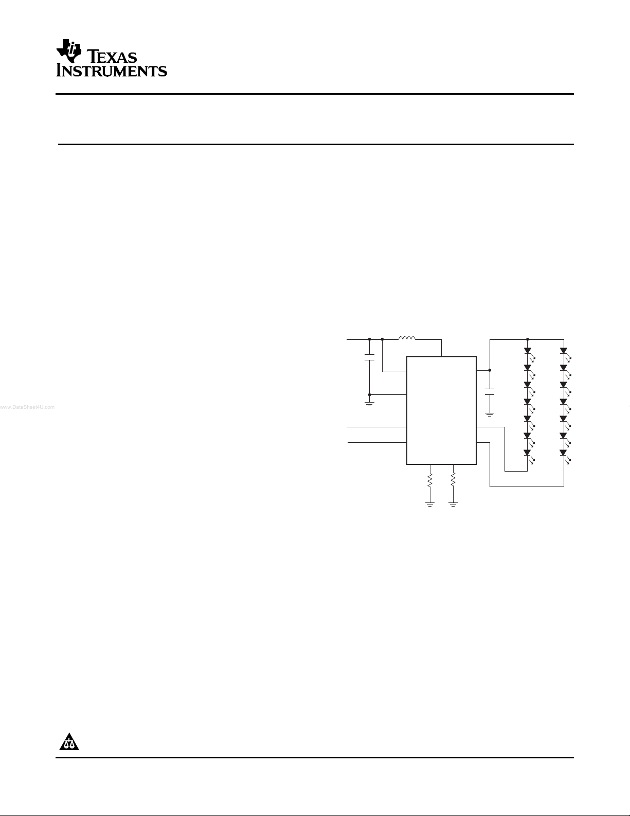
VIN
SW
GND
SEL2
SEL1
ISET1
IFB1
R1
56.5kW
IOUT
IFB2
ISET2
R2
56.5kW
2.5Vto6VInput
L1
10 Hm
C1
1mF
C2
1mF
TPS61150A
DUAL OUTPUT BOOST WLED DRIVER
USING SINGLE INDUCTOR
TPS61150A
SLVS706 – OCTOBER 2006
FEATURES
• 2.5V to 6V Input Voltage Range
• 0.7A Integrated Switch
• Built-in Power Diode
• 1.2MHz Fixed PWM Frequency
• Individually Programmable Output Current
• Input-to-Output Isolation
• Built-in Soft Start
• 27V Overvoltage Protection
• 3% at 15mA Matching between Two Current
Strings, Improvement from TPS61150/1
• Up to 83% Efficiency
• Up to 30kHz PWM Dimming Frequency
• Availiable in a 10 Pin, 3 × 3 mm QFN Package
APPLICATIONS
• Up to 14 WLED Driver for Media Form Factor
Display
• Sub and Main Display Backlight in Clam Shell
Phones
• Display and Keypad Backlight in Portable
Equipment
The two current outputs are ideal for driving WLED
backlight for the sub and main displays in clam shell
phones. The two outputs can also be used for driving
display and keypad backlights. When used together,
the two outputs can drive up to 14 WLED for one
large display.
In addition to the small inductor, small capacitor and
3mm x 3mm QFN package, the built-in MOSFET and
diode eliminate the need for any external power
devices. Overall, the IC provides an extremely
compact solution with high efficiency and plenty of
flexibility.
TYPICAL APPLICATION
DESCRIPTION
The TPS61150A is a high frequency boost converter
with two regulated current outputs for driving
WLEDs. Each current output can be individually
programmed through external resistors. There is
dedicated selection pin for each output, so the two
outputs can be turned on separately or
simultaneously. The output current can be reduced
by a pulse width modulation (PWM) signal on the
select pins or an analog voltage on the ISET pin. The
boost regulator runs at 1.2MHz fixed switching
frequency to reduce output ripple and avoid audible
noises associated with PFM control.
Please be aware that an important notice concerning availability, standard warranty, and use in critical applications of Texas
Instruments semiconductor products and disclaimers thereto appears at the end of this data sheet.
PRODUCTION DATA information is current as of publication date.
Products conform to specifications per the terms of the Texas
Instruments standard warranty. Production processing does not
necessarily include testing of all parameters.
Copyright © 2006, Texas Instruments Incorporated
www.ti.com
1
2
3
4
5
10
9
8
7
6
IFB1
ISET
SEL1
SEL2
VIN
IFB2
ISET2
GND
IOUT
SW
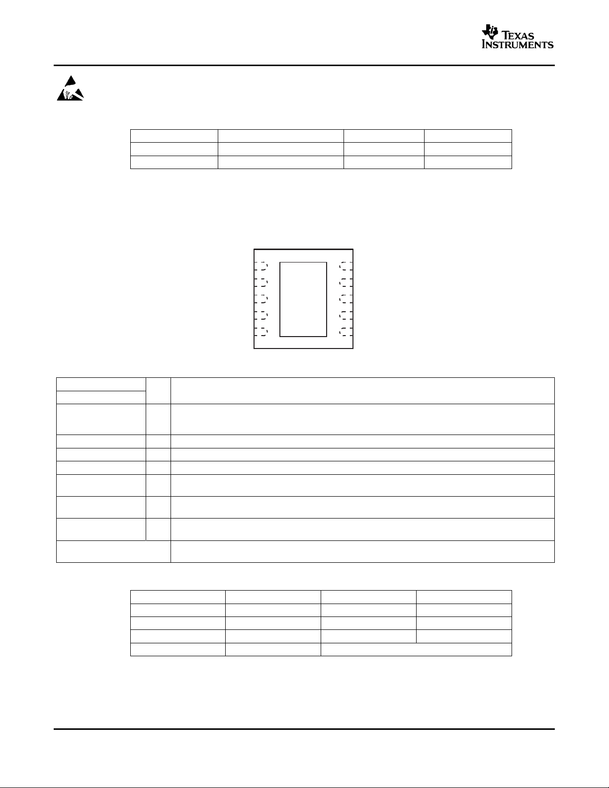
QFNPACKAGE
(TOP VIEW)
Exposed
Thermal
Pad
TPS61150A
SLVS706 – OCTOBER 2006
These devices have limited built-in ESD protection. The leads should be shorted together or the device placed in conductive foam
during storage or handling to prevent electrostatic damage to the MOS gates.
ORDERING INFORMATION
T
A
–40 to 85 ° C TPS61150ADRCR 28V BTK
–40 to 85 ° C TPS61150ADRCT 28V BTK
(1) For the most current package and ordering information, see the Package Option Addendum at the end
of this document, or see the TI website at www.ti.com .
PACKAGE OVP (Typ.) PACKAGE MARKING
(1)
DEVICE INFORMATION
TERMINAL FUNCTIONS
TERMINAL
NAME NO.
VIN 5 I below the undervoltage lockout threshold, the IC turns off and disables outputs; thereby disconnecting the
GND 8 O Ground. Connect the input and output capacitors as close as possible to this pin.
SW 6 I Switching node of the IC.
IOUT 7 O Constant current supply output. IOUT is directly connected to the boost converter output.
IFB1, IFB2 10 I
ISET1, 2
ISET2 9
SEL1, 3
SEL2 4
Thermal Pad
I/O DESCRIPTION
Input pin. VIN provides the current to the boost power stage, and also powers the IC circuit. When VIN is
WLEDs from the input.
Return path for the IOUT regulation. The current regulator is connected to this pin, and it can be disabled
to open the current path.
I Output current programming. The resistor connected to the pin programs the corresponding output current.
I Mode selection. See Table 1 for details.
The thermal pad should be soldered to the analog ground. If possible, use the thermal pad to connect to
ground plane for ideal power dissipation.
2
Table 1. TPS61150A Mode Selection
SEL1 SEL2 IFB1 IFB2
H L Enable Disable
L H Disable Enable
H H Enable Enable
L L IC Shutdown
Submit Documentation Feedback
www.ti.com
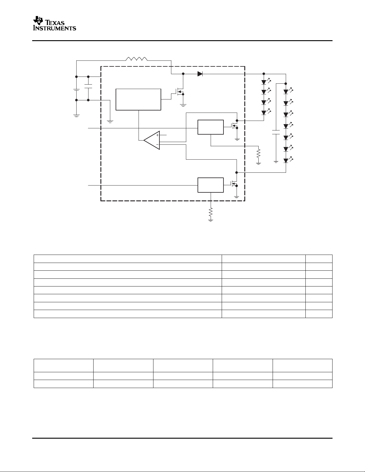
FUNCTIONAL BLOCK DIAGRAM
VIN
IFB2
IOUT
SW
Error
Amplifier
Current
Sink
SEL1
SEL2
GND
ISET2
TPS61150A
Current
Sink
0.33V
IFB1
ISET1
+
−
1.2MHzCurrent
ModeControl
PWM
TPS61150A
SLVS706 – OCTOBER 2006
ABSOLUTE MAXIMUM RATINGS
(1)
over operating free-air temperature range (unless otherwise noted)
VALUE UNIT
Supply voltages on pin VIN
Voltages on pins SEL1/2, ISET1/2
Voltage on pin IOUT, SW, IFB1 and IFB2
Continuous power dissipation See Dissipation Rating Table
Operating junction temperature range –40 to 150 ° C
Storage temperature range –65 to 150 ° C
Lead Temperature (soldering, 10 sec) 260 ° C
(1) Stresses beyond those listed under absolute maximum ratings may cause permanent damage to the device. These are stress ratings
only, and functional operation of the device at these or any other conditions beyond those indicated under recommended operating
conditions is not implied. Exposure to absolute-maximum-rated conditions for extended periods may affect device reliability.
(2) All voltage values are with respect to network ground terminal.
DISSIPATION RATINGS
PACKAGE R
(1)
QFN
(2)
QFN
(2 48.7
(1) Soldered PowerPAD on a standard 2-layer PCB without vias for thermal pad.
(2) Soldered PowerPAD on a standard 4-layer PCB with vias for thermal pad .
(2)
(2)
(2)
TA≤ 25 ° C TA= 70 ° C TA= 85 ° C
θ JA
o
270
C/W 370mW 204mW 148mW
o
C/W 2.05W 1.13W 821mW
POWER RATING POWER RATING POWER RATING
–0.3 to 7 V
–0.3 to 7 V
30 V
Submit Documentation Feedback
3
www.ti.com
TPS61150A
SLVS706 – OCTOBER 2006
RECOMMENDED OPERATING CONDITIONS
over operating free-air temperature range (unless otherwise noted)
V
I
V
O
L Inductor
C
I
C
O
T
A
T
J
(1) See Application Section for further information.
Input voltage range 2.5 6.0 V
Output voltage range VIN 27 V
(1)
Input capacitor
Output capacitor
(1)
(1)
Operating ambient temperature –40 85 ° C
Operating junction temperature –40 125 ° C
MIN NOM MAX UNIT
10 µ H
1 µ F
1 µ F
4
Submit Documentation Feedback
www.ti.com
ELECTRICAL CHARACTERISTICS
VIN = 3.6V, SELx = VIN, Rset = 80k Ω , V
noted)
PARAMETER TEST CONDITIONS MIN TYP MAX UNIT
SUPPLY CURRENT
V
I
I
Q
I
SD
V
UVLO
V
hys
ENABLE AND SOFT START
V
(selh)
V
(sell)
R
(en)
t
(off)
I
(ss)
t
(ss)
t
(ss_en)
CURRENT FEEDBACK
V
(ISET)
K
ISET
K
M
V
(IFB)
V
hys(IFB_L)
t
I(sink)
I
lkg
POWER SWITCH AND DIODE
R
DS(ON)
I
lkg(N_NFET)
V
(F)
OC AND OVP
I
L
I
(IFB_MAX)
V
ovp
V
ovp_hys
PWM AND PFM CONTROL
F
S
D
max
THERMAL SHUTDOWN
T
shutdown
T
hys
Input voltage range 2.5 6.0 V
Operating quiescent current into VIN Device PWM switching no load 2 mA
Shutdown current SELx = GND, TA= 25 ° C 1.7 1.9 µ A
Under-voltage lockout threshold VIN falling 1.65 1.8 V
Under-voltage lockout hysterisis 70 mV
SEL logic high voltage VI= 2.5V to 6V 1.2 V
SEL logic low voltage VI= 2.5V to 6V 0.4 V
SEL pull down resistor 300 700 k Ω
SEL pulse width to disable SELx high to low 40 ms
IFB soft start current steps 16
Soft start time step Measured as clock divider 64
Soft start enable time Time between falling and rising of two adjacent 40 ms
ISET pin voltage 1.204 1.229 1.254 V
Current multipler, I
Current matching, (2 × |I
/I
, I
fb1
set1
–I
fb1
IFB regulation voltage 300 330 360 mV
IFB low threshold hysteresis 60 mV
Current sink settle time measured from 6 µ s
SELx rising edge
(1)
IFB pin leakage current IFB voltage = 25V 1 µ A
N-channel MOSFET on-resistance VIN= V
N-channel leakage current V
Power diode forward voltage Diode current = 0.7A 0.83 1.0 V
N-Channel MOSFET current limit A
Current sink max output current IFB current = 330mV 34 mA
Overvoltage threshold 27 28 29 V
Overvoltage hysteresis 550 mV
Oscillator frequency 1.0 1.2 1.5 MHz
Maximum duty cycle Feedback voltage = 1.0V 89% 93%
Thermal shutdown threshold 160 ° C
Thermal shutdown threshold hysteresis 15 ° C
TPS61150A
SLVS706 – OCTOBER 2006
= 15V, TA= –40 ° C to 85 ° C, typical values are at TA= 25 ° C (unless otherwise
(IOUT)
SELx = GND 2.7 3
SELx pulses
/I
fb2
set2
|)/(I
fb2
fb1
ISET current = 16.7 µ A 883 920 957
ISET current = 1.2 µ A 736 920 1104
+I
) ISET current = 16.7 µ A 0% 3%
fb2
ISET current = 1.2 µ A 0% 20%
= 3.6V 0.6 0.9 Ω
GS
= 25V 1 µ A
DS
Dual output, IOUT= 15V, Duty cycle = 76% 0.75 1.0 1.25
Single output , IOUT= 15V, Duty cycle = 76% 0.40 0.55 0.7
(1) This specification determines the minimum on time required for PWM dimming for desirable linearity. The maximum PWM dimming
frequency can be calculated from the minimum duty cycle required in the application.
Submit Documentation Feedback
5
www.ti.com
0
100
200
300
400
500
600
10 20 30 40 50 60 70 80 90
DutyCycle-%
CurrentLimit-mA
V =4.2V
I
V =3.6V
I
V =3V
I
0
200
400
600
800
1000
1200
10 20 30 40 50 60 70 80 90
DutyCycle-%
CurrentLimit-mA
VI=4.2V
V =3.6V
I
V =3V
I
TPS61150A
SLVS706 – OCTOBER 2006
TYPICAL CHARACTERISTICS
Table of Graphs
Overcurrent Limit VIN = 3.0V, 3.6V, and 4.2V, single and dual output 1,2
WLED efficiency VIN = 3.3V, 3.6V and 4.2V, 3 WLED, WLED voltage = 11V 3
WLED efficiency VIN = 3.3V, 3.6V and 4.2V, 4 WLED, WLED voltage = 15V 4
WLED efficiency VIN = 3.3V, 3.6V and 4.2V, 5 WLED, WLED voltage = 19V 5
WLED efficiency VIN = 3.3V, 3.6V and 4.2V, 6 WLED, WLED voltage = 23V 6
Both on efficiency VIN = 3.3V, 3.6V and 4.2V, 4 WLED on each output 7
K value over current VIN = 3.6V, I
PWM dimming linearity Frequency = 20kHz and 30kHz 9
Single output PWM dimming waveform 10
Multiplexed PWM dimming waveform 11
Start up waveform 12
= 1mA to 25mA 8
WLED
FIGURES
OVERCURRENT LIMIT (SINGLE OUTPUT) OVERCURRENT LIMIT (DUAL OUTPUT)
vs vs
DUTY CYCLE DUTY CYCLE
Figure 1. Figure 2.
6
Submit Documentation Feedback
www.ti.com
50
60
70
80
90
0 5 10 15 20 25
WLEDCurrent-mA
Efficiency-%
WLEDVoltage=11V ,3WLED,
SingleOutput
V =3.6V
I
V =3.3V
I
V =4.2V
I
50
60
70
80
90
0 5 10 15 20 25
WLEDCurrent-mA
Efficiency-%
WLEDVoltage=15V,4WLED,
SingleOutput
V =4.2V
I
V =3.3V
I
V =3.6V
I
50
60
70
80
90
0 5 10 15 20 25
WLEDCurrent-mA
Efficiency-%
WLEDVoltage=19V,5WLED,
SingleOutput
V =4.2V
I
V =3.3V
I
V =3.6V
I
50
60
70
80
90
0 5 10 15 20 25
WLEDCurrent-mA
Efficiency-%
WLEDVoltage=23V,6WLED,
SingleOutput
V
I
V =4.2V
I
V =3.6V
I
=3.3V
EFFICIENCY EFFICIENCY
vs vs
LOAD CURRENT LOAD CURRENT
Figure 3. Figure 4.
TPS61150A
SLVS706 – OCTOBER 2006
EFFICIENCY EFFICIENCY
vs vs
LOAD CURRENT LOAD CURRENT
Figure 5. Figure 6.
Submit Documentation Feedback
7
www.ti.com
700
800
900
1000
1100
1200
0 10 20 30 40 50
WLEDCurrent-mA
V =3.6V
WLED1Voltage=15V
WLED2Voltage=15V
I
KValue
WLED1
WLED2
50
60
70
80
90
0 10 20 30 40
60
50
I -TotalOutputCurrent-mA
O
Efficiency-%
WLED1Voltage=15V
WLED2Voltage=15V
V =3.3V
I
V =4.2V
I
V =3.6V
I
ISEL2
5V/div ,DC
WLEDCurrent
20mA/div,DC
IOUT
1V/div ,DC
15VOffset
SW
10V/div ,DC
t-Time-20 s/divm
0
5
10
15
20
25
0
20 40 60
80 100
PWMDutycycle-%
WLEDcurrent-mA
f=20kHz
f=30kHz
TPS61150A
SLVS706 – OCTOBER 2006
BOTH ON EFFICIENCY K VALUE
vs vs
TOTAL OUTPUT CURRENT WLED CURRENT
Figure 7. Figure 8.
SINGLE OUTPUT WLED PWM
WLED BRIGHTNESS DIMMING LINEARITY BRIGHTNESS DIMMING
8
Figure 9. Figure 10.
Submit Documentation Feedback

www.ti.com
ISEL2
5V/div ,DC
IOUT
10V/div ,DC
WLEDCurrent
20mA/div ,DC
t-Time-200 s/divm
InductorCurrent
500mA/div ,DC
ISEL1
5V/div ,DC
ISEL2
5V/div ,DC
t-Time-2ms/div
IOUT
5V/div ,DC
MULTIPLEXED PWM DIMMING
(ISEL1: 4 WLED, ISEL2: 2 WLED) WLED START UP
Figure 11. Figure 12.
TPS61150A
SLVS706 – OCTOBER 2006
Submit Documentation Feedback
9

www.ti.com
I
O
+
V
ISET
R
SET
K
ISET
TPS61150A
SLVS706 – OCTOBER 2006
DETAILED DESCRIPTION
CURRENT REGULATION
The TPS61150A uses a single boost regulator to drive 2 WLED strings whose current can be programmed
independently. The boost converter adopts PWM control which is ideal for high output current and low output
ripple noises. The feedback loop regulates the IFB pin to a threshold voltage (330mV typical), giving the current
sink circuit just enough headroom to operate.
The regulation current is set by the resistor on the Iset pin based on
where
IO= output current
V
= Iset pin voltage (1.229V typical)
ISET
R
= Iset pin resistor value
SET
K
= current multiplier (920 typical)
ISET
When both outputs are enabled, the boost converter regulates to the IFB pin that demands higher Iout pin
voltage, V
switches to the other IFB pin if its voltage drops more than the IFB low hysterisis (60mV typical) below it's
regulation voltage. This ensures proper current regulation for both outputs. When both IFB voltages are low,
IFB1 is used for regulation. Once IFB1 reaches its regulation voltage, the feedback path may hand over to IFB2
if it is still low, and the boost output will continue to rise.
The overall efficiency in this mode depends on the voltage different between the IFB1 and IFB2. A large
difference reduces the efficiency due to power losses across the current sink circuit. To improve the efficiency of
the both-on mode, the two current outputs can be turned on complimentarily by applying out of phase enable
signal to the SEL pins. The ISET pin resistors need to be recalculated to compensate for the reduced DC
current.
, and let the other IFB pin rise above its regulation voltage. The feedback path dynamically
(IOUT)
(1)
START UP
During start up, both the boost converter and the current sink circuitry are trying to establish steady state
simultaneously. The current sink circuitry ramps up current in 16 steps, with each step taking 64 clock cycles.
This ensures that the current sink loop is slower than the boost converter response during startup. Therefore,
the boost converter output comes up slowly as current sink circuitry ramps up the current. This ensures smooth
start up and minimizes in-rush current.
OVERVOLTAGE PROTECTION
To prevent the boost output run away as the result of WLED disconnection, there is an overvoltage protection
circuit which stops the boost converter from switching as soon as its output exceeds the OVP threshold. When
the voltage falls below the OVP threshold, the converter resumes switching. TPS61150A provides 28V(typical)
OVP to prevent a 25V rated output capacitor or the internal 30V FET from breaking down.
UNDERVOLTAGE LOCKOUT
An undervoltage lockout prevents mis-operation of the device for input voltages below 1.65V (typical). When the
input voltage is below the undervoltage threshold, the device remains off and both the boost converter and
current sink circuit are turned off, providing isolation between input and output.
THERMAL SHUTDOWN
An internal thermal shutdown turns off the IC when the typical junction temperature of 160 ° C is exceeded. The
thermal shutdown has a hysteresis of typically 15 ° C.
10
Submit Documentation Feedback

www.ti.com
TPS61150A
SLVS706 – OCTOBER 2006
DETAILED DESCRIPTION (continued)
ENABLE
Pulling either the SEL1 or SEL2 pin low turns off the corresponding output. If both SEL1 and SEL2 are low for
more than 40ms, the IC shuts down and consumes less than 2 µ A (room temperature) current. The SEL pin can
also be used for PWM brightness dimming. To improve PWM dimming linearity, soft start is disabled if the time
between falling and rising edges of two adjacent SELx pulses is less than 40ms. See APPLICATION
INFORMATION for details.
Each SEL input pin has an internal pull down resistor to disable the device when the pin is floating.
Submit Documentation Feedback
11
www.ti.com
I
p
+
1
ƪ
L
ǒ
1
Viout)Vf*Vin
)
1
Vin
Ǔ
Fs
ƫ
Iout_max +
Vin ǒIlim*
I
p
2
Ǔ h
Viout
ISET
Q1
R1
R
ISET
ON/OFF
Logic
TPS61150A
SLVS706 – OCTOBER 2006
APPLICATION INFORMATION
MAXIMUM OUTPUT CURRENT
The over-current limit in a boost converter limits the maximum input current and thus maximum input power for a
given input voltage. Maximum output power is less than maximum input power due to power conversion losses.
Therefore, the current limit, input voltage, output voltage and efficiency can all change maximum current output.
Since current limit clamps peak inductor current, ripple has to be subtracted to derive maximum DC current. The
ripple current is a function of switching frequency, inductor value and duty cycle. The following equations take
into account of all the above factors for maximum output current calculation.
where
Ip = inductor peak-to-peak ripple
L = inductor value
Vf = power diode forward voltage
Fs = switching frequency
Viout = boost output voltage. It is equal to 330mV + voltage drop across WLED.
(2)
where
Iout_max = maximum output current of the boost converter
Ilim = overcurrent limit
η = efficiency
To keep a tight range of the overcurrent limit, The TPS61150A uses the Vin and Iout pin voltage to compensate
for the overcurrent limit variation caused by the slope compensation. However, the current threshold still has
residual dependency on the VIN and IOUT voltage. Use Figure 1 and Figure 2 to identify the typical overcurrent
limit in your application, and use ± 25% tolerance to account for temperature dependency and process variations.
The maximum output current can also be limited by the current capability of the current sink circuitry. It is
designed to provide maximum 35mA current regardless of the current capability of the boost converter.
WLED BRIGHTNESS DIMMING
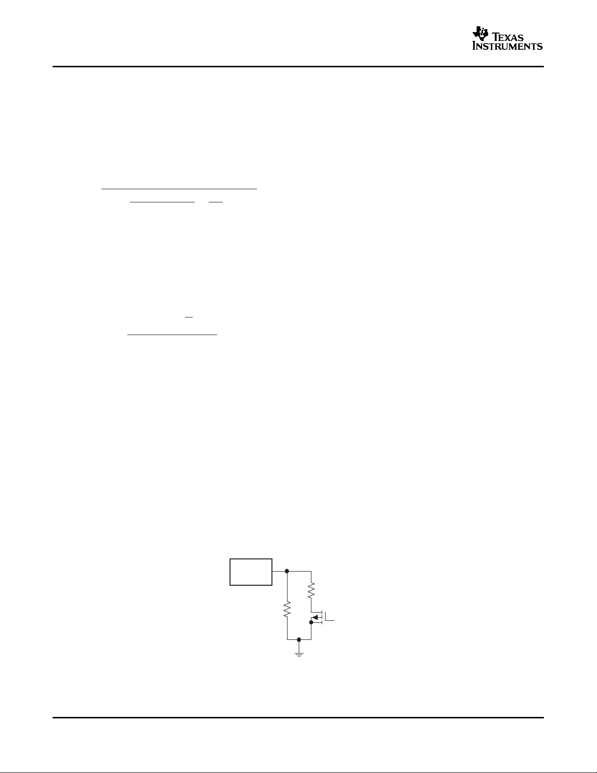
There are three ways to change the output current on the fly for WLED dimming. The first method parallels an
additional resistor with the ISET pin resistor as shown in Figure 13 . The switch (Q1) can change the ISET pin
resistance and therefore, modify the output current. This method is very simple, but can only provide limited
dimming steps.
(3)
12
Figure 13. Switching In/Out an Additional Resistor to Change Output Current
Submit Documentation Feedback
www.ti.com
F
PWM_MAX
+
D
min
T
isink
I
WLED
+ K
ISET
ǒ
1.229
R
ISET
)
1.229* V
DC
R
1
Ǔ
for DC voltage input
I
WLED
+ K
ISET
ǒ
1.229
R
ISET
)
1.229* V
DC
R1) 10K
Ǔ
for PWM signal input
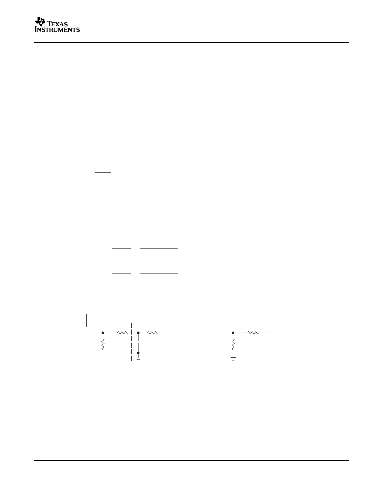
Filter
ISET
PWM Signal
0.1 mF
10 kWR1
R
ISET
ISET
DC Voltage
R1
R
ISET
TPS61150A
SLVS706 – OCTOBER 2006
APPLICATION INFORMATION (continued)
Alternatively, a PWM dimming signal at the SEL pin can modulate the output current by the duty cycle of the
signal. The logic high of the signal turns on the current sink circuit, while the logic low turns it off. This operation
creates an averaged DC output current proportional to the duty cycle of the PWM signal. The frequency of the
PWM signal has to be high enough to avoid flashing of the WLEDs. The soft start of the current sink circuit is
disabled during the PWM dimming to improve linearity.
The major concern of the PWM dimming is the creation of audible noises which can come from the inductor
and/or output capacitor of the boost converter. The audible noises on the output capacitor are created by the
presence of voltage ripple in range of audible frequencies. The TPS61150A alleviates the problem by
disconnecting the WLEDs from the output capacitor when the SEL pin is low. Therefore, the output capacitor is
not discharged by the WLEDs, which reduces the voltage ripple during PWM dimming.
The audible noises can be eliminated by using PWM dimming frequency above or below the audible frequency
range. The maximum PWM dimming frequency of the TPS61150A is determined by the current settling time
(t
) which is the time required for the circuit sink circuit to reach steady state after the SEL pin transitions from
isink
low to high. The maximum dimming frequency can be calculated by
D
= min duty cycle of the PWM dimming required in the application.
min
For 20% D
range.
The third method uses an external DC voltage and resistor as shown in Figure 14 to change the ISET pin
current, and thus control the output current. The DC voltage can be the output of a filtered PWM signal. The
equation to calculate the output current is
, PWM dimming frequency up to 33kHz is possible, making the noise frequency above the audible
min
(4)
K
= current multiplier between the ISET pin current and the IFB pin current.
ISET
VDC= voltage of the DC voltage source or the DC voltage of the PWM signal.
Figure 14. Analog Dimming Uses an External Voltage Source to Control the Output Current
INDUCTOR SELECTION
Because the selection of the inductor affects power supplies steady state operation, transient behavior, and loop
stability, the inductor is the most important component in power regulator design. There are three specifications
most important to the performance of the inductor, inductor value, DC resistance, and saturation current.
Considering inductor value alone is not enough.
The inductors inductance value determines the inductor ripple current. It is generally recommended to set
peak-to-peak ripple current given by Equation 2 to 30–40% of DC current. It is a good compromise of power
losses and inductor size. For this reason, 10 µ H inductors are recommended for TPS61150A. Inductor DC
current can be calculated as
Submit Documentation Feedback
(5)
(6)
13

www.ti.com
I
L_DC
+
V
iout
I
out
V
in
h
C
out
+
ǒ
V
iout
* V
in
Ǔ
I
out
V
iout
Fs V
ripple
TPS61150A
SLVS706 – OCTOBER 2006
APPLICATION INFORMATION (continued)
Use the maximum load current and minimum VIfor calculation.
The internal loop compensation for PWM control is optimized for the external component shown in the typical
application circuit with consideration of component tolerance. Inductor values can have ± 20% tolerance with no
current bias. When the inductor current approaches saturation level, its inductance can decrease 20 to 35%
from the 0A value depending on how the inductor vendor defines saturation. Using an inductor with a smaller
inductance value forces discontinuous PWM in which inductor current ramps down to zero before the end of
each switching cycle. It reduces the boost converter’s maximum output current, and causes large input voltage
ripple. An inductor with larger inductance reduces the gain and phase margin of the feedback loop, possibly
resulting in instability
Regulator efficiency is dependent on the resistance of its high current path and switching losses associated with
the PWM switch and power diode. Although the TPS61150A has optimized the internal switches, the overall
efficiency still relies on inductors DC resistance (DCR); Lower DCR improves efficiency. However, there is a
trade off between DCR and inductor size, and shielded inductors typically have higher DCR than unshielded
ones. DCR in range of 150m Ω to 350m Ω is suitable for applications requiring both on mode. DCR is the range
of 250m Ω to 450m Ω is a good choice for single output application. Table 2 and Table 3 list recommended
inductor models.
Table 2. Recommended Inductors for Single Output
L DCR Typ Isat SIZE
( µ H) (m Ω ) (A) (L × W × H mm)
TDK
VLF3012AT-100MR49 10 360 0.49 2.8 × 3.0 × 1.2
VLCF4018T-100MR74-2 10 163 0.74 4.0 × 4.0 × 1.8
Sumida
CDRH2D11/HP 10 447 0.52 3.2 × 3.2 × 1.2
CDRH3D16/HP 10 230 0.84 4.0 × 4.0 × 1.8
(7)
Table 3. Recommended Inductors for Dual Output
L DCR Typ Isat SIZE
( µ H) (m Ω ) (A) (L × W × H mm)
TDK
VLCF4018T-100MR74-2 10 163 0.74 4.0 × 4.0 × 1.8
VLF4012AT-100MR79 10 300 0.85 3.5 × 3.7 × 1.2
Sumida
CDRH3D16/HP 10 230 0.84 4.0 × 4.0 × 1.8
CDRH4D11/HP 10 340 0.85 4.8 × 4.8 × 1.2
INPUT AND OUTPUT CAPACITOR SELECTION
The output capacitor is mainly selected for the output ripple of the converter. This ripple voltage is the sum of the
ripple caused by the capacitor’s capacitance and its equivalent series resistance (ESR). Assuming a capacitor
with zero ESR, the minimum capacitance needed for a given ripple can be calculated by
V
= Peak-to-peak output ripple.
ripple
14
Submit Documentation Feedback
(8)
www.ti.com
TPS61150A
SLVS706 – OCTOBER 2006
For VI= 3.6V, V
= 20V, and Fs= 1.2MHz, 0.1% ripple (20mV) would require 1.0 µ F capacitor. For this value,
iout
ceramic capacitors are the best choice for its size, cost and availability.
The additional output ripple component caused by ESR is calculated using:
V
ripple_ESR
Due to it's low ESR, V
= I
× R
out
ESR
ripple_ESR
can be neglected for ceramic capacitors, but must be considered if tantalum or
electrolytic capacitors are used.
During a load transient, the capacitor at the output of the boost converter has to supply or absorb additional
current before the inductor current ramps up the steady state value. Larger capacitors always help to reduce the
voltage over and under shoot during a load transient. A larger capacitor also helps loop stability.
Care must be taken when evaluating a ceramic capacitor’s derating due to applied dc voltage, aging and
frequency response. For example, larger form factor capacitors (in 1206 size) have their self-resonant
frequencies in the range of TPS61150A’s switching frequency, so the effective capacitance is significantly lower.
Therefore, it may be necessary to use small capacitors in parallel instead of one large capacitor.
The popular vendors for high value ceramic capacitors are:
TDK (http://www.component.tdk.com/components.php )
Murata (http://www.murata.com/cap/index.html )
Table 4. Recommended Input and Output Capacitors
Capacitance ( µ F) Voltage (V) Case
TDK
C3216X5R1E475K 4.7 25 1206
C2012X5R1E105K 1 25 805
C1005X5R0J105K 1 6.3 402
Murata
GRM319R61E475KA12D 4.7 25 1206
GRM216R61E105KA12D 1 25 805
GRM155R60J105KE19D 1 6.3 402
LAYOUT CONSIDERATION
As for all switching power supplies, especially those providing high current and using high switching frequencies,
layout is an important design step. If layout is not carefully done, the regulator could show instability as well as
EMI problems, therefore, use wide and short traces for high current paths. The input capacitor needs not only to
be close to the VIN pin, but also to the GND pin in order to reduce the input ripple seen by the IC. The VIN and
SW pins are conveniently located on the edges of the IC, therefore the inductor can be placed close to the IC.
The output capacitor needs to be placed near the load to minimize ripple and maximize transient performance.
It is also beneficial to have the ground of the output capacitor close to the GND pin since there will be large
ground return current flowing between them. When laying out signal ground, it is recommended to use short
traces separated from power ground traces, and connect them together at a single point.
Submit Documentation Feedback
15

www.ti.com
SW
SEL1
ISET1
ISET2
VIN
IFB2
IOUT
SEL2
EN/PWM
Dimming
GND
VIN
IFB1
C2
1 Fm
1 Fm
R2R1
C2
L1
10 Hm
SEL1
SEL2
IFB1
ON
IFB1
ON
IFB2
ON
IFB2
ON
40ms
Display
Keypad
VIN
SW
GND
SEL2
SEL1
ISET1
IFB1
L1
10 Hm
R1
IFB2
ISET2
R2
IOUT
C2
IC
Shutdown
VIN
C1
1 Fm
1 Fm
TPS61150A
SLVS706 – OCTOBER 2006
ADDITIONAL APPLICATION CIRCUIT
Figure 15. Driving Up to 12 WLEDs With One LCD Backlight
Figure 16. Driving a Keypad and LCD Backlight by applying interleaved PWM signal to the SEL1 and
SEL2 pins. The duty cycle of the PWM signal controls brightness dimming
16
Submit Documentation Feedback

PACKAGE OPTION ADDENDUM
www.ti.com
5-Feb-2007
PACKAGING INFORMATION
Orderable Device Status
(1)
Package
Type
Package
Drawing
Pins Package
Qty
Eco Plan
TPS61150ADRCR ACTIVE SON DRC 10 3000 Green (RoHS &
no Sb/Br)
TPS61150ADRCRG4 ACTIVE SON DRC 10 3000 Green (RoHS &
no Sb/Br)
TPS61150ADRCT ACTIVE SON DRC 10 250 Green (RoHS &
no Sb/Br)
TPS61150ADRCTG4 ACTIVE SON DRC 10 250 Green (RoHS &
no Sb/Br)
(1)
The marketing status values are defined as follows:
ACTIVE: Product device recommended for new designs.
LIFEBUY: TI has announced that the device will be discontinued, and a lifetime-buy period is in effect.
NRND: Not recommended for new designs. Device is in production to support existing customers, but TI does not recommend using this part in
a new design.
PREVIEW: Device has been announced but is not in production. Samples may or may not be available.
OBSOLETE: TI has discontinued the production of the device.
(2)
Eco Plan - The planned eco-friendly classification: Pb-Free (RoHS), Pb-Free (RoHS Exempt), or Green (RoHS & no Sb/Br) - please check
http://www.ti.com/productcontent for the latest availability information and additional product content details.
TBD: The Pb-Free/Green conversion plan has not been defined.
Pb-Free (RoHS): TI's terms "Lead-Free" or "Pb-Free" mean semiconductor products that are compatible with the current RoHS requirements
for all 6 substances, including the requirement that lead not exceed 0.1% by weight in homogeneous materials. Where designed to be soldered
at high temperatures, TI Pb-Free products are suitable for use in specified lead-free processes.
Pb-Free (RoHS Exempt): This component has a RoHS exemption for either 1) lead-based flip-chip solder bumps used between the die and
package, or 2) lead-based die adhesive used between the die and leadframe. The component is otherwise considered Pb-Free (RoHS
compatible) as defined above.
Green (RoHS & no Sb/Br): TI defines "Green" to mean Pb-Free (RoHS compatible), and free of Bromine (Br) and Antimony (Sb) based flame
retardants (Br or Sb do not exceed 0.1% by weight in homogeneous material)
(2)
Lead/Ball Finish MSL Peak Temp
CU NIPDAU Level-2-260C-1 YEAR
CU NIPDAU Level-2-260C-1 YEAR
CU NIPDAU Level-2-260C-1 YEAR
CU NIPDAU Level-2-260C-1 YEAR
(3)
(3)
MSL, Peak Temp. -- The Moisture Sensitivity Level rating according to the JEDEC industry standard classifications, and peak solder
temperature.
Important Information and Disclaimer:The information provided on this page represents TI's knowledge and belief as of the date that it is
provided. TI bases its knowledge and belief on information provided by third parties, and makes no representation or warranty as to the
accuracy of such information. Efforts are underway to better integrate information from third parties. TI has taken and continues to take
reasonable steps to provide representative and accurate information but may not have conducted destructive testing or chemical analysis on
incoming materials and chemicals. TI and TI suppliers consider certain information to be proprietary, and thus CAS numbers and other limited
information may not be available for release.
In no event shall TI's liability arising out of such information exceed the total purchase price of the TI part(s) at issue in this document sold by TI
to Customer on an annual basis.
Addendum-Page 1

PACKAGE MATERIALS INFORMATION
www.ti.com
17-May-2007
TAPE AND REEL INFORMATION
Pack Materials-Page 1

PACKAGE MATERIALS INFORMATION
www.ti.com
Device Package Pins Site Reel
Diameter
(mm)
TPS61150ADRCR DRC 10 MLA 330 12 3.3 3.3 1.1 8 12 PKGORN
TPS61150ADRCT DRC 10 MLA 180 12 3.3 3.3 1.1 8 12 PKGORN
Reel
Width
(mm)
A0 (mm) B0 (mm) K0 (mm) P1
(mm)W(mm)
17-May-2007
Pin1
Quadrant
T2TR-MS
P
T2TR-MS
P
TAPE AND REEL BOX INFORMATION
Device Package Pins Site Length (mm) Width (mm) Height (mm)
TPS61150ADRCR DRC 10 MLA 346.0 346.0 29.0
TPS61150ADRCT DRC 10 MLA 190.0 212.7 31.75
Pack Materials-Page 2

PACKAGE MATERIALS INFORMATION
www.ti.com
17-May-2007
Pack Materials-Page 3


IMPORTANT NOTICE
Texas Instruments Incorporated and its subsidiaries (TI) reserve the right to make corrections, modifications, enhancements,
improvements, and other changes to its products and services at any time and to discontinue any product or service without notice.
Customers should obtain the latest relevant information before placing orders and should verify that such information is current and
complete. All products are sold subject to TI’s terms and conditions of sale supplied at the time of order acknowledgment.
TI warrants performance of its hardware products to the specifications applicable at the time of sale in accordance with TI’s
standard warranty. Testing and other quality control techniques are used to the extent TI deems necessary to support this
warranty. Except where mandated by government requirements, testing of all parameters of each product is not necessarily
performed.
TI assumes no liability for applications assistance or customer product design. Customers are responsible for their products and
applications using TI components. To minimize the risks associated with customer products and applications, customers should
provide adequate design and operating safeguards.
TI does not warrant or represent that any license, either express or implied, is granted under any TI patent right, copyright, mask
work right, or other TI intellectual property right relating to any combination, machine, or process in which TI products or services
are used. Information published by TI regarding third-party products or services does not constitute a license from TI to use such
products or services or a warranty or endorsement thereof. Use of such information may require a license from a third party under
the patents or other intellectual property of the third party, or a license from TI under the patents or other intellectual property of TI.
Reproduction of information in TI data books or data sheets is permissible only if reproduction is without alteration and is
accompanied by all associated warranties, conditions, limitations, and notices. Reproduction of this information with alteration is an
unfair and deceptive business practice. TI is not responsible or liable for such altered documentation.
Resale of TI products or services with statements different from or beyond the parameters stated by TI for that product or service
voids all express and any implied warranties for the associated TI product or service and is an unfair and deceptive business
practice. TI is not responsible or liable for any such statements.
TI products are not authorized for use in safety-critical applications (such as life support) where a failure of the TI product would
reasonably be expected to cause severe personal injury or death, unless officers of the parties have executed an agreement
specifically governing such use. Buyers represent that they have all necessary expertise in the safety and regulatory ramifications
of their applications, and acknowledge and agree that they are solely responsible for all legal, regulatory and safety-related
requirements concerning their products and any use of TI products in such safety-critical applications, notwithstanding any
applications-related information or support that may be provided by TI. Further, Buyers must fully indemnify TI and its
representatives against any damages arising out of the use of TI products in such safety-critical applications.
TI products are neither designed nor intended for use in military/aerospace applications or environments unless the TI products are
specifically designated by TI as military-grade or "enhanced plastic." Only products designated by TI as military-grade meet military
specifications. Buyers acknowledge and agree that any such use of TI products which TI has not designated as military-grade is
solely at the Buyer's risk, and that they are solely responsible for compliance with all legal and regulatory requirements in
connection with such use.
TI products are neither designed nor intended for use in automotive applications or environments unless the specific TI products
are designated by TI as compliant with ISO/TS 16949 requirements. Buyers acknowledge and agree that, if they use any
non-designated products in automotive applications, TI will not be responsible for any failure to meet such requirements.
Following are URLs where you can obtain information on other Texas Instruments products and application solutions:
Products Applications
Amplifiers amplifier.ti.com Audio www.ti.com/audio
Data Converters dataconverter.ti.com Automotive www.ti.com/automotive
DSP dsp.ti.com Broadband www.ti.com/broadband
Interface interface.ti.com Digital Control www.ti.com/digitalcontrol
Logic logic.ti.com Military www.ti.com/military
Power Mgmt power.ti.com Optical Networking www.ti.com/opticalnetwork
Microcontrollers microcontroller.ti.com Security www.ti.com/security
RFID www.ti-rfid.com Telephony www.ti.com/telephony
Low Power www.ti.com/lpw Video & Imaging www.ti.com/video
Wireless
Wireless www.ti.com/wireless
Mailing Address: Texas Instruments, Post Office Box 655303, Dallas, Texas 75265
Copyright © 2007, Texas Instruments Incorporated
 Loading...