

(3,25 mm x 3,25 mm)
www.ti.com
C
IN
L1
V
IN
22 µF
4.7 µH
2.7 V . . 5.5 V
GND
TPS61058
GND
PVIN
EN
VIN
SW VOUT
FB
PGND
C1, C2, C3
x3
D1
C3
Rs
R2
R1
IOK
R3
R4
FLASH ON (0/1.8 V)
22 µF
39 kΩ
22 kΩ
56 kΩ
1.5 Ω
62 kΩ
1 nF
(COG)
R5
5.6 kΩ
0
10
20
30
40
50
60
70
80
90
100
2.70 3.10 3.50 3.90 4.30 4.70 5.10 5.50
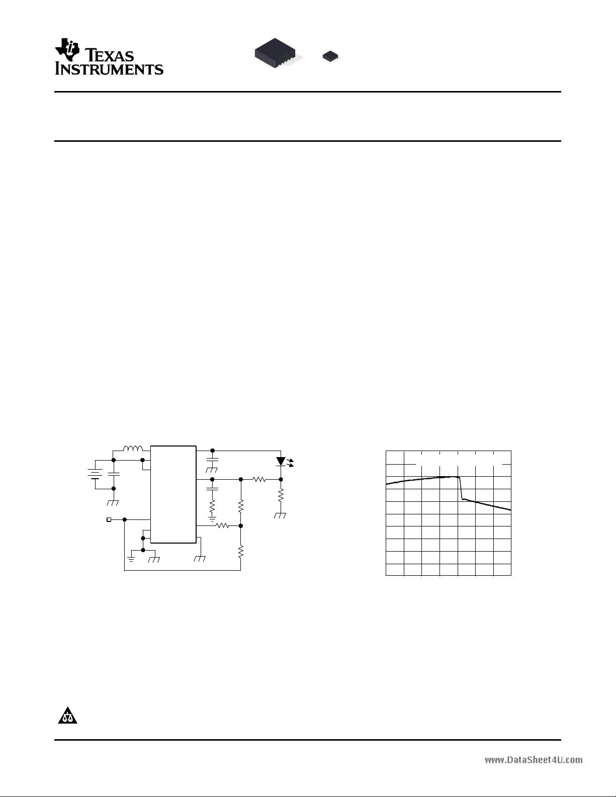
V - Input Voltage - V
I
LED Power Efficiency (P /P ) - %
LED IN
I = 500 mA @ V = 3.7 V
LED F
SYNCHRONOUS BOOST CONVERTER WITH DOWN MODE
HIGH POWER WHITE LED DRIVER
FEATURES DESCRIPTION
• 80% Efficient Synchronous Boost Converter
– 500-mA LED Current From 3.3-V Input
(TPS61058)
– 800-mA LED Current From 3.3-V Input
(TPS61059)
• Input Voltage Range: 2.7 V to 5.5 V
• Fixed Frequency 650 kHz (Typ) Operation
• LED Disconnect During Shutdown
• Open/Shorted LED Protection
• Over-Temperature Protection
• Low Shutdown Current: 100 nA (Typ)
• Total Solution Of Less Than 80 mm
• Small 3mm x 3mm QFN-10 Package
APPLICATIONS
• Torch/Camera White LED Supply for Cell
Phones, Smart-Phones and PDAs
TPS61058
TPS61059
SLVS572B – APRIL 2005 – REVISED DECEMBER 2005
The TPS61058/9 devices are fixed frequency,
synchronous boost dc-dc converters with an
integrated down conversion mode. The devices are
optimized for driving high power single cell white
LEDs up to 800 mA from a 2.7-V to 5.5-V input. The
LED current can be programmed to different levels
(e.g. torch, flashlight) by a set of external resistors.
The boost converter is based on a 650 kHz fixed
frequency, pulse-width-modulation (PWM) controller
using a synchronous rectifier to obtain maximum
efficiency. The maximum peak current in the boost
switch is limited to 1000 mA (TPS61058) and 1500
2
mA (TPS61059).
The converter can be disabled to maximize battery
life. In the shutdown mode, the load is completely
disconnected and the current consumption is reduced
to less than 1 µA. Built-in precharge and soft-start
circuitry prevents excessive inrush current during
start-up.
The device is packaged in a 10-pin QFN
PowerPAD™ package measuring 3 mm x 3 mm
(DRC).
Figure 1. 500 mA Flashlight Application
Please be aware that an important notice concerning availability, standard warranty, and use in critical applications of Texas
Instruments semiconductor products and disclaimers thereto appears at the end of this data sheet.
PowerPAD is a trademark of Texas Instruments.
PRODUCTION DATA information is current as of publication date.
Products conform to specifications per the terms of the Texas
Instruments standard warranty. Production processing does not
necessarily include testing of all parameters.
Figure 2. Flashlight Efficiency vs V
Copyright © 2005, Texas Instruments Incorporated
IN
www.ti.com
TPS61058
TPS61059
SLVS572B – APRIL 2005 – REVISED DECEMBER 2005
These devices have limited built-in ESD protection. The leads should be shorted together or the device placed in conductive foam
during storage or handling to prevent electrostatic damage to the MOS gates.
AVAILABLE OPTIONS
T
A
-40 ° C to 85 ° C 10-Pin QFN
(1) The DRC package is available taped and reeled. Add R suffix to device type (e.g. TPS61058DRCR, TPS61059DRCR) to order
quantities of 3000 devices per reel.
(2) For the most current package and ordering information, see the Package Option Addendum at the end of this document, or see the TI
website at www.ti.com.
CURRENT LIMIT PACKAGE MARKING PACKAGE PART NUMBER
1000 mA BNF TPS61058DRC
1500 mA BNG TPS61059DRC
ABSOLUTE MAXIMUM RATINGS
over operating free-air temperature range (unless otherwise noted)
Input voltage range on PVIN, VIN, EN, FB, IOK, SW, VOUT -0.3 V to 7 V
Power dissipation Internally limited
Operation temperature range, T
Maximum operating junction temperature, TJ(max) 150 ° C
Storage temperature range, T
(1) Stresses beyond those listed under "absolute maximum ratings" may cause permanent damage to the device. These are stress ratings
only, and functional operation of the device at these or any other conditions beyond those indicated under "recommended operating
conditions" is not implied. Exposure to absolute-maximum-rated conditions for extended periods may affect device reliability.
A
stg
(1)
TPS61058/9
-40 ° C to 85 ° C
-65 ° C to 150 ° C
(1) (2)
DISSIPATION RATINGS TABLE
PACKAGE
DRC 48.7 ° C/W 2040 mW 21 mW/ ° C
THERMAL RESISTANCE POWER RATING DERATING FACTOR ABOVE
Θ
JA
TA≤ 25 ° C TA= 25 ° C
2
www.ti.com
SLVS572B – APRIL 2005 – REVISED DECEMBER 2005
ELECTRICAL CHARACTERISTICS
V
= 3.6 V, I
IN
otherwise noted)
DC/DC STAGE
V
IN
V
OUT
V
OVP
V
FB
f Oscillator frequency 550 650 750 kHz
I
SW
r
DS(on)
I
Q
I
(SD)
CONTROL STAGE
V
(IL)
V
(IH)
I
(I)
= 500 mA, EN = VIN, L = 4.7 µH, C
LED
= 3x 22 µF, TA= –40 ° C to 85 ° C, typical values are at TA= 25 ° C (unless
O
PARAMETER TEST CONDITIONS MIN TYP MAX UNIT
Input voltage range VO> 2.0 V @ I
= 50 mA 2.7 5.5 V
LED
TPS61058/9 output voltage range 2.5 5.5 V
Output overvoltage protection 5.9 6.1 6.3 V
TPS61058/9 feedback voltage 490 500 510 mV
Switch current limit (TPS61058) VO= 3.3 V 900 1100 1300 mA
Switch current limit (TPS61059) VO= 3.3 V 1200 1500 1800 mA
Pre-charge current VO= 2.5 V, TA= -10 ° C to 85 ° C 84 mA
SWN switch on resistance VO= 3.3V 260 m Ω
SWP switch on resistance VO= 3.3 V 290 m Ω
Total accuracy (including line and load regulation) -3% 3%
I
= 0 mA, VO= 5.0 V,
Quiescent current 5.5 mA
LED
Device switching at 650 kHz
Shutdown current EN = GND, TA= 25 ° C 0.1 1 µA
IOK switch on-resistance VO= 5.0 V, I
= 100 µA 0.6 0.8 1 k Ω
IOK
IOK output low current 100 300 µA
IOK output leakage current V
= 7 V 0.01 0.1 µA
IOK
EN low-level input voltage 0.4 V
EN high-level input voltage 1.4 V
EN input leakage current Input tied to GND 0.01 0.1 µA
EN pull-down resistance 400 k Ω
Overtemperature protection 140 ° C
Overtemperature hysteresis 20 ° C
TPS61058
TPS61059
3
www.ti.com
FB
IOK
GND
PVIN
SW
VOUT
GND
VIN
EN
PGND
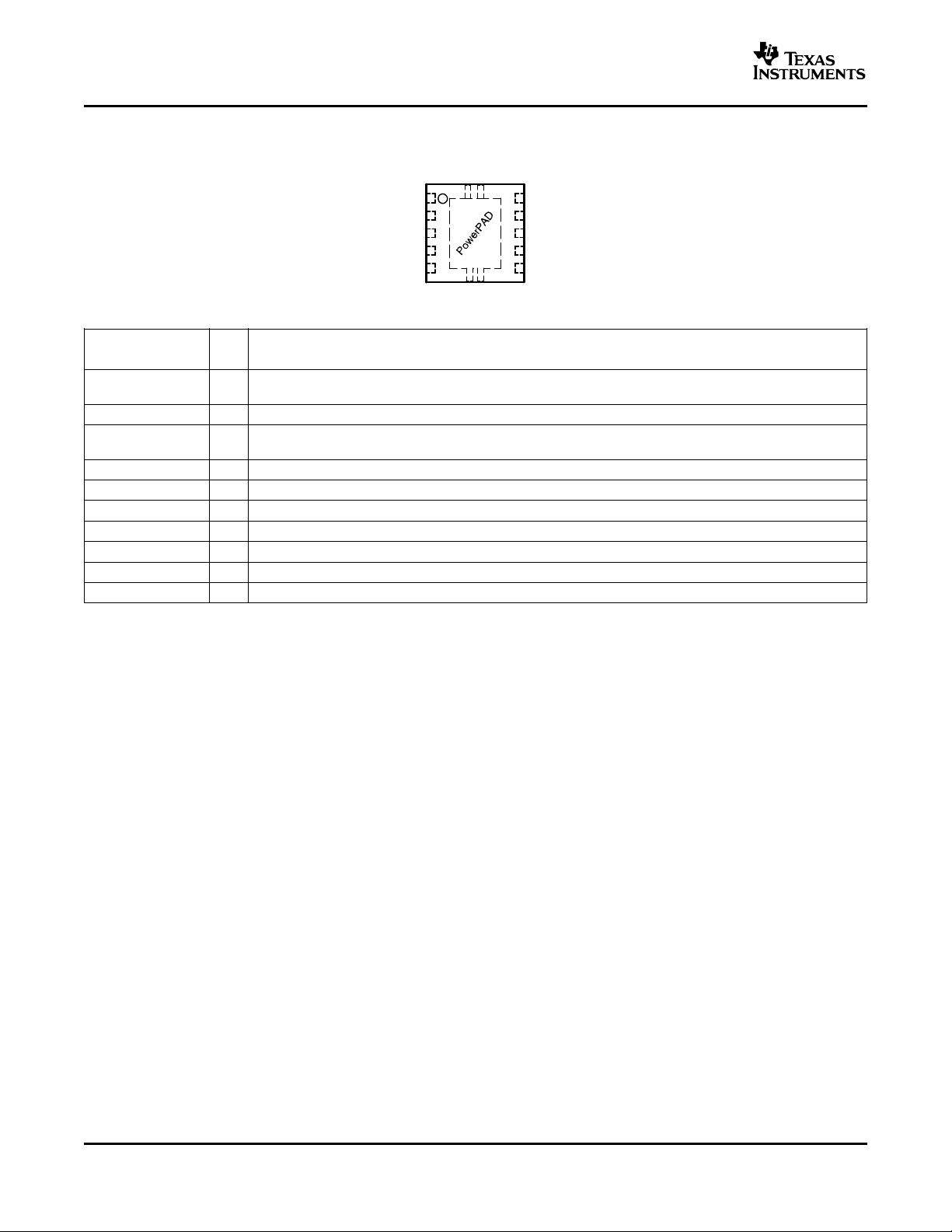
DRC Package
(TOP VIEW)
TPS61058
TPS61059
SLVS572B – APRIL 2005 – REVISED DECEMBER 2005
PIN ASSIGNMENTS
Terminal Functions
TERMINAL
NAME NO.
EN 1 I This is the enable pin of the device. Connect this pin to ground forces the device into shutdown mode. Pulling
VOUT 2 O This is the output of the dc-dc converter.
FB 3 I This is the feedback pin of the device. The feedback pin measures the LED current through the sense
IOK 4 O This pin indicates that the dc-dc converter is ready for high current operation (open drain output).
GND 5, 7 Control / logic ground.
PVIN 6 I This is the input voltage pin of the device. Connect directly to the input bypass capacitor.
VIN 8 I This pin needs to be tied to the input voltage pin of the device.
SW 9 I This is the switching pin of the converter.
PGND 10 Power ground.
PowerPAD™ Must be soldered to achieve appropriate power dissipation. Should be connected to PGND.
I/O DESCRIPTION
this pin above 1.4V enables the device. This pin has an internal pull-down resistor.
resistor. The feedback voltage is set internally to 500mV.
4
www.ti.com
Vmax
control
Gate
Control
Regulator Error-
Amplifier
Vref
Oscillator
PGND
PVIN
SW
VOUT
FB
GND
EN
PGND
GND
VIN
OVP
Vref
EN
Control Logic
PGND
20 pF
Temperature
Control
10 kW
IOK
400 kW
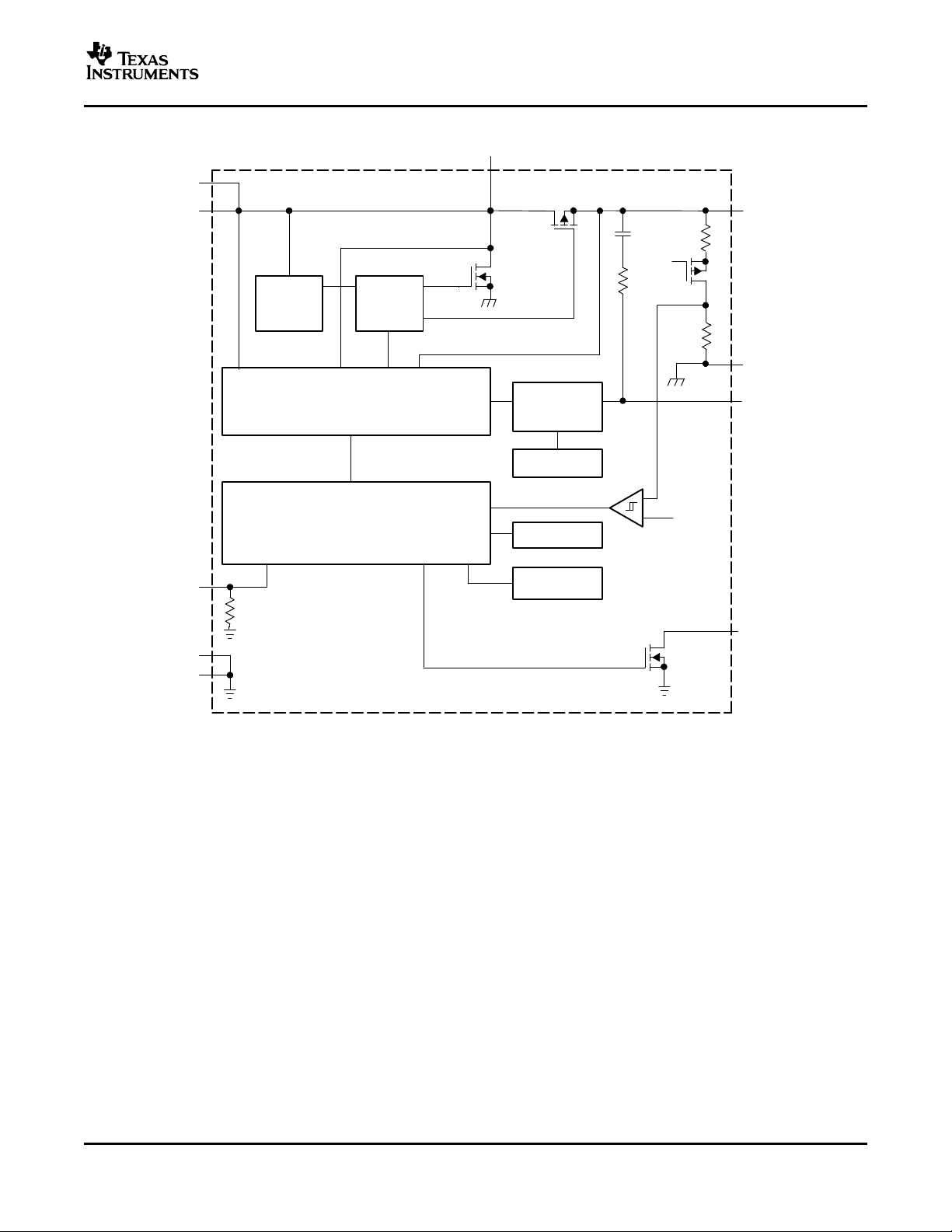
FUNCTIONAL BLOCK DIAGRAM (TPS61058/9)
TPS61058
TPS61059
SLVS572B – APRIL 2005 – REVISED DECEMBER 2005
5
www.ti.com
C
IN
L1
V
IN
22 Fm
4.7 Fm
2.7 V . . 5.5 V
GND
TPS61058/9
GND
PVIN
EN
VIN
SW VOUT
FB
PGND
C1, C2, C3
x3
D1
C3
Rs
R2
R1
IOK
R3
R4
TORCH ON (0/1.8 V)
22 Fm
22 kW
1 nF (COG)
R6
R5
FLASH (0 . .2 V)
500 mA Flashlight Application
Rs = 1.3
R2 = 56 k
R3 = 100 k
R4 = 2.4 k
R5 = 6.2 k
R6 = 91 k
W
W
W
W
W
W
700 mA Flashlight Application
Rs = 1.2
R2 = 47 k
R3 = 51 k
R4 = 3.3 k
R5 = 4.3 k
R6 = 120 k
W
W
W
W
W
W
List of Components:
L1 = TDK VLF5014AT-4R7T
C1,C2,C3 = TDK C2012X5R0J226MTJ
C4
(Optional)
C4 = 100 nF
TPS61058
TPS61059
SLVS572B – APRIL 2005 – REVISED DECEMBER 2005
PARAMETER MEASUREMENT INFORMATION
TYPICAL CHARACTERISTICS
Table of Graphs
FIGURE
(TPS61058) LED Power Efficiency vs. Input Voltage 3
(TPS61059) LED Power Efficiency vs. Input Voltage 4
(TPS61058) LED Power Efficiency vs LED Current 5
(TPS61058) DC Input Current vs. Input Voltage 6
(TPS61058) LED Current vs. Input Voltage 7
Oscillator Frequency 8
(TPS61059) Current Limit vs. Temperature 9
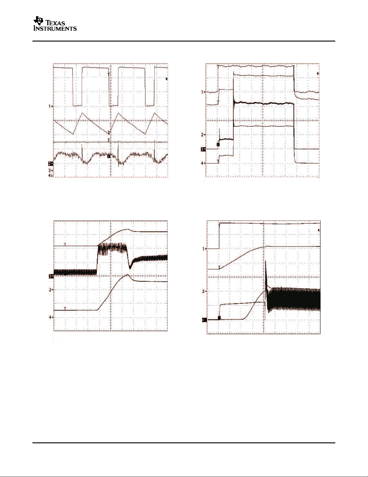
Waveforms Switching Waveforms in Boost Mode (TPS61058) 10
Switching Waveforms in Down-Mode (TPS61058) 11
High Current Flashlight Pulse Waveform (TPS61058) 12
Torch to Flashlight Transistion (TPS61058) 13
Start-Up After Enable (TPS61058) 14
Overvoltage Protection (TPS61058) 15
Duty Cycle Jitter (TPS61058) 16
6
www.ti.com
0
10
20
30
40
50
60
70
80
90
100
2.70 3.10 3.50 3.90 4.30 4.70 5.10 5.50
LEDPowerEfficiency(P /P )-%
LED IN
I = 500 mA @ V = 3.7 V
LED F
I = 150 mA @ V = 3.4 V
LED F
V - Input Voltage - V
I
0
10
20
30
40
50
60
70
80
90
100
2.70 3.10 3.50 3.90 4.30 4.70 5.50
VI − Input Voltage − V
LED Power Efficiency (P
LED
/P
IN
) − %
I
LED
= 700 mA @ VF = 3.4 V
I
LED
= 150 mA @ VF = 3.0 V
5.10
0
200
400
600
800
1000
1200
1400
2.70 3.10 3.50 3.90 4.30 4.70 5.10 5.50
Input DC Current - mA
V - Input Voltage - V
I
I = 500 mA
LED
0
10
20
30
40
50
60
70
80
90
100
100 150 200 250 300 350 400 450 500
LED Current - mA
LED Power Efficiency (P /P ) - %
LED IN
V = 3.3 V
IN
V = 4.2 V
IN
V = 3.6 V
IN
TPS61058
TPS61059
SLVS572B – APRIL 2005 – REVISED DECEMBER 2005
LED POWER EFFICIENCY LED POWER EFFICIENCY
TPS61058 TPS61059
vs vs
INPUT VOLTAGE INPUT VOLTAGE
Figure 3. Figure 4.
TPS61058 TPS61058
EFFICIENCY DC INPUT CURRENT
vs vs
LED CURRENT INPUT VOLTAGE
Figure 5. Figure 6.
7
www.ti.com
0
100
200
300
400
500
600
2.70 3.10 3.50 3.90 4.30 4.70 5.10 5.50
LED Current - mA
I = 500 mA
LED
I = 150 mA
LED
V - Input Voltage - V
I
0
2
4
6
8
10
12
14
16
606
615
622
629
636
643
650
657
664
672
f − Oscillator Frequency − kHz
Percent of Units − %
TA = 25C
Switch Current Limit − Am
Ambient Temperature − C
1250
1350
1450
1550
1650
1750
-40 -30 -20 -10 0 10 20 30 40 50 60 70 80
SW (2 V/div)
V = 3.6 V, I = 500 mA
I LED
I (200 mA/div)
L
V (10 mV/div - 3.8 V OFFSET)
OUT
I (200 mA/div)
LED
t - Time - 500 ns/div
TPS61058
TPS61059
SLVS572B – APRIL 2005 – REVISED DECEMBER 2005
TPS61058 OSCILLATOR FREQUENCY
LED CURRENT
vs
INPUT VOLTAGE
Figure 7. Figure 8.
TPS61059 TPS61058
CURRENT LIMIT SWITCHING WAVEFORMS IN BOOST MODE
TEMPERATURE
Figure 9. Figure 10.
8
vs
www.ti.com
SW
(2 V/div)
I (200 mA/div)
L
I (200mA/div)
LED
V
(10 mV/div - 3.8 V OFFSET)
OUT
V = 4.5 V, I = 500 mA
I LED
t - Time - 500 ns/div
EN (1 V/div)
t - Time - 5 ms/div
I (200 mA/div)
L
V (1 V/div)
OUT
I (200 mA/div)
LED
V = 3.6 V
I
V (1 V/div)
OUT
I (200 mA/div)
LED
I (500 mA/div)
L
t - Time - 50 s/divm
EN (1 V/div)
V (1 V/div)
OUT
I (50 mA/div)
LED
I (100 mA/div)
L
t - Time - 200 s/divm
TPS61058
TPS61059
SLVS572B – APRIL 2005 – REVISED DECEMBER 2005
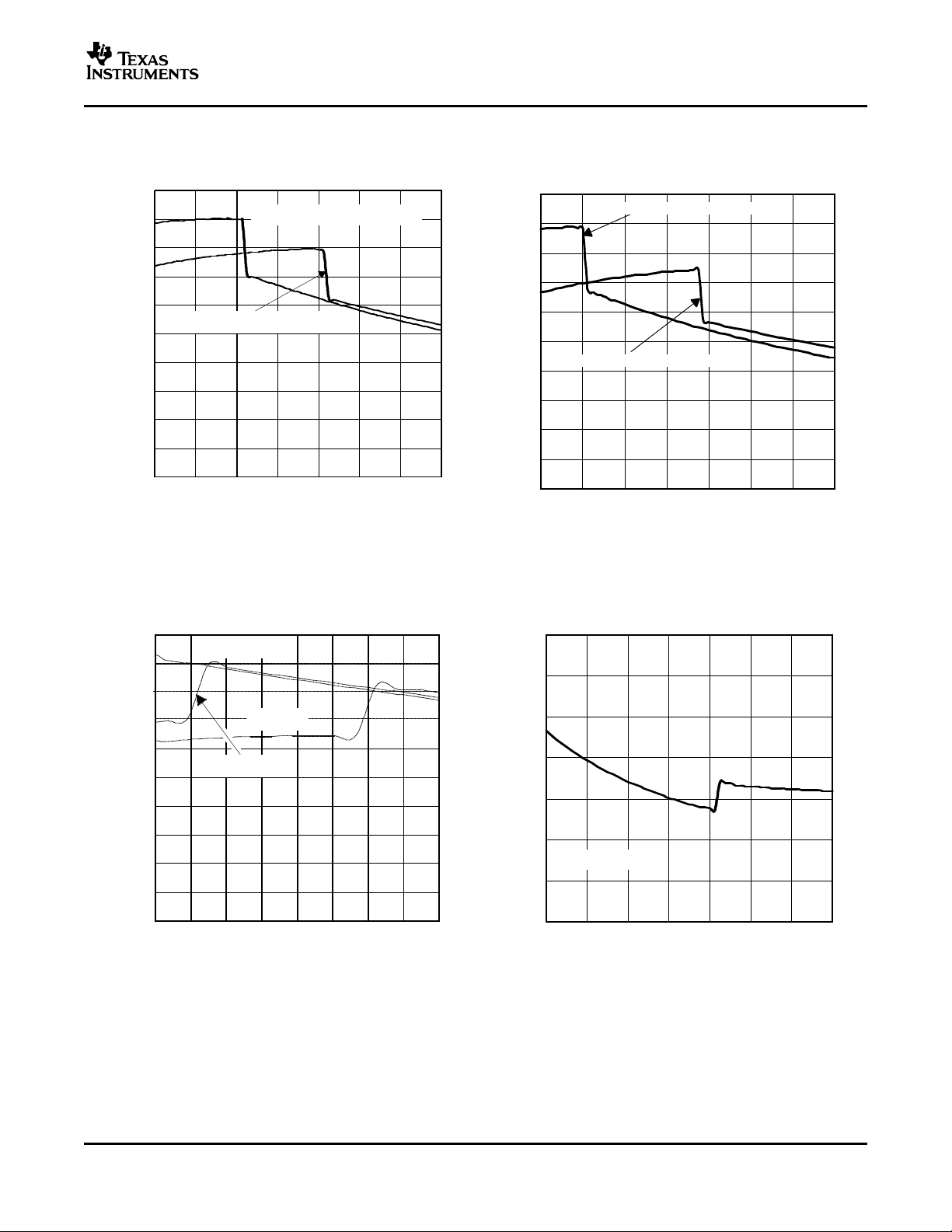
SWITCHING WAVEFORMS IN DOWN MODE HIGH CURRENT FLASHLIGHT PULSE WAVEFORM
TPS61058 TPS61058
Figure 11. Figure 12.
TPS61058 TPS61058
TORCH TO FLASHLIGHT TRANSISTION START-UP AFTER ENABLE
Figure 13. Figure 14.
9

www.ti.com
SW (2 V/div)
V = 3.6 V
I
I = 500 mA
LED
Triggered On Falling Edge
t - Time - 50 ns/div
V (200 mV/div - 5 V OFFSET)
OUT
t - Time - 50 ms/div
TPS61058
TPS61059
SLVS572B – APRIL 2005 – REVISED DECEMBER 2005
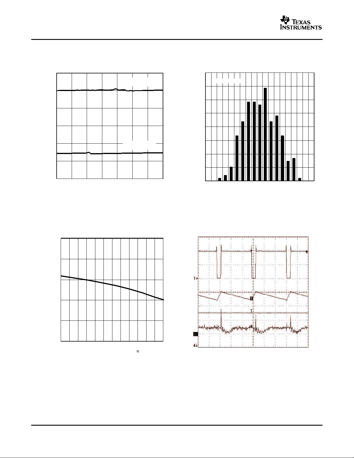
OVERVOLTAGE PROTECTION DUTY CYCLE JITTER
TPS61058 TPS61058
Figure 15. Figure 16.
10

www.ti.com
TPS61058
TPS61059
SLVS572B – APRIL 2005 – REVISED DECEMBER 2005
DETAILED DESCRIPTION
OPERATION
The TPS61058/9 familly is based on a fixed frequency multiple feedforward controller topology. Input voltage,
output voltage, and voltage drop on the NMOS switch are monitored and forwarded to the regulator. So changes
in the operating conditions of the converter directly affect the duty cycle and must not take the indirect and slow
way through the control loop and the error amplifier.
The control loop, determined by the error amplifier, only has to handle small signal errors. The input for it is the
feedback voltage on the FB pin. It is compared with the internal reference voltage to generate an accurate and
stable LED current.
The peak current of the NMOS switch is also sensed to limit the maximum current flowing through the switch and
the inductor. The typical peak current limit is set to 1000mA (TPS61058) and 1500 mA (TPS61059). An internal
temperature sensor prevents the device from getting overheated in case of excessive power dissipation.
Synchronous Rectifier
The device integrates an N-channel and a P-channel MOSFET transistor to realize a synchronous rectifier.
Because the commonly used discrete Schottky rectifier is replaced with a low RDS(ON) PMOS switch, the power
conversion stage itself can reach 96% efficiency.
In order to avoid ground shift due to the high currents in the NMOS switch, two separate ground pins are used.
The reference for all control functions is the GND pin. The source of the NMOS switch is connected to PGND.
Both grounds must be connected on the PCB at only one point close to the GND pin.
A special circuit is applied to disconnect the load from the input during shutdown of the converter. In conventional
synchronous rectifier circuits, the backgate diode of the high-side PMOS is forward biased in shutdown and
allows current flow from the battery to the output. This device however uses a special circuit which takes the
cathode of the backgate diode of the high-side PMOS and disconnects it from the source when the regulator is
not enabled (EN = Low).
The benefit of this feature for the system design engineer is that the battery is not depleted during shutdown of
the converter. No additional components have to be added to the design to make sure that the battery is
disconnected from the output of the converter.
Down Regulation
In general, a boost converter only regulates output voltages which are higher than the input voltage. This device
operates differently and is capable of driving high power single die white LEDs from a fully charged Li-Ion cell. To
control this applications properly, a down conversion mode is implemented.
If the input voltage reaches or exceeds the output voltage necessary to maintain the LED current within
regulation, the converter changes to a down conversion mode. In this mode, the control circuit changes the
behavior of the rectifying PMOS transitor. It sets the voltage drop across the PMOS as high as needed to
regulate the output voltage. This means the power losses in the converter increase. This has to be taken into
account for thermal consideration especially when operating with low V
LEDs, high battery voltages and high
F
LED currents.
Enable
The device is put into operation when EN is set high. It is put into a shutdown mode when EN is set to GND. The
EN input pin has an internal 400-k Ω pull-down resistor to disable the device when this pin is floating.
In shutdown mode, the regulator stops switching, the internal control circuitry is switched off, and the load is
isolated from the input (as described in the Synchronous Rectifier Section). This also means that the output
voltage can drop below the input voltage during shutdown.
11

www.ti.com
TPS61058
TPS61059
SLVS572B – APRIL 2005 – REVISED DECEMBER 2005
DETAILED DESCRIPTION (continued)
Softstart
To avoid high inrush current during start-up, special care is taken to control the inrush current. When the device
is first enabled, the output capacitor is charged with a constant pre-charge current of 115mA (typ) until either the
output voltage is typically 0.1V below the input voltage or the feedback voltage is 500mV (typ). The rectifying
switch is current limited during the pre-charge phase. This also limits the output current under short circuit
conditions at the output.
The fixed pre-charge current during start-up allows the device to start up without problems when driving single
die white LEDs as long as the LED start-up current is set to a value lower than the pre-charge current (84 mA
min.). Refer to the application section for more details.
When the device has finished start-up and is ready for high current operation, the device forces IOK output to
ground, starts switching and regulates the LED current to the desired value (e.g. torch or flashlight current level).
Overvoltage Protection (OVP)
As with any current source, the output voltage rises when the load becomes high impedance or gets
disconnected. To prevent the output voltage exceeding the maximum switch voltage rating (7 V) of the main
switch, an overvoltage protection circuit is integrated. As soon as the output voltage exceeds the OVP threshold,
the converter stops switching and the output voltage decreases. When the output voltage falls below the OVP
threshold, the converter continues operation until the output voltage exceeds the OVP threshold again.
Efficiency and Sense Voltage
The voltage across the sense resistor (R
voltage does not contribute to the output power (P
) has a direct effect of the converter efficiency. Because the sense
S
), the lower this voltage the higher the efficiency. It is
LED
therefore recommended to operate with a sense voltage of approximately 0.75V at maximum LED current.
Thermal Shutdown
An internal thermal shutdown is implemented and turns off the internal MOSFETs when the typical junction
temperature of 140 ° C is exceeded. The thermal shutdown has a hysteresis of typically 20 ° C. Refer to the
Thermal Information section.
12

www.ti.com
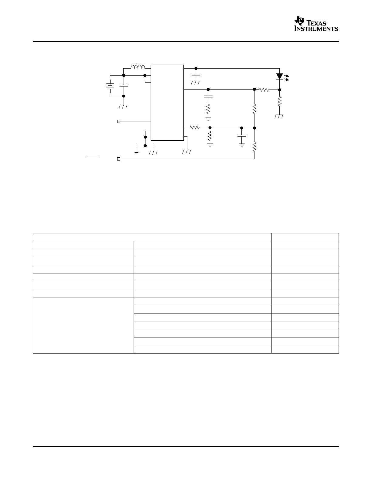
nFLASH
IOK
ILED
Flashlight
MOVIE-LIGHT
Hi-Z Hi-Z
Pre-Charge
Movie-Light
GND
C
IN
L1
GND
PVIN
EN
VIN
SW
VOUT
FB
PGND
V
IN D1
Rs
R2
R3
R4
nFLASH
IOK Vx
R6
R5
2.7 V . . 5.5 V
4.7 µH
22 µF
MOVIE-LIGHT
C1, C2, C3
22 µF
x3
C4
1 nF (COG)
R1
22 kΩ
V
SENSE
TPS61058/9
C5
100nF
R
S
V
SENSE
I
LED
SLVS572B – APRIL 2005 – REVISED DECEMBER 2005
APPLICATION INFORMATION
DESIGN PROCEDURE
The standard application circuit (Figure 17 ) of the TPS61058/9 is a complete solution to drive high-power white
LEDs with two discrete current steps.
TPS61058
TPS61059
Figure 17. Typical Application
The LED current is programmed using external resistors (R
the LED is to enable the device (EN = High). After charging the output capacitor, the device forces IOK to
ground, starts switching, and regulates the LED current to the desired value. The control signal, nFLASH, injects
current into the feedback network through R4, thereby, changing the LED current. For this reason, the nFLASH
control signal needs at least to be biased up until IOK goes low. In case this is not done properly the converter
stays stuck in the pre-chage phase.
To faciliate the sizing of the external resistor network, it is recommended to use the calculation sheet available in
the device product folder.
1. Sense resistor, R
S
The voltage across the sense resistor should be set to approximately 0.75 V at maximum LED current.
Check the power rating of the sense resistor (P
2. LED current setting
Figure 19 shows an equivalent circuit for the feedback network. The regulation loop is using an external
control voltage (nFLASH) to set the LED current. With the help of this voltage the feedback bias current
(I
) can be adjusted which, in effect, controls the LED current without changing any externals.
BIAS
In most applications a variable control voltage is not available to set the LED current. In practical
applications, nFLASH can either be:
A constant bias voltage (2.8 V for example) which in combination with IOK can be used to switch
between two LED currents (Off, Flashlight).
A logic signal generated by the imaging processor. This configuration permits three different LED
currents: Off, Movie-light (nFLASH = High), Flashlight (nFLASH = Low).
Figure 18. Waveform Profiles
, R2, R3, R4, R5, and R6). The first step to turn on
S
(1)
= RS× I
D
2
).
LED
13

www.ti.com
I
LED
0.5 R2 I
BIAS
R
S
I
BIAS
R5
R3 (R4 R5)
nFLASH
0.5
R3
, assuming R4R5 is small compared R3.
I
LED
0.5 R2 I
BIAS2
R
S
1
2 R
S
R2
2 R3 R
S
R2
R3 R
S
Vx
I
BIAS2
R5
R3 (R4 R5)
nFLASH
0.5
R3
, with R5
R5 R6
R5 R6
I
LED(FLASH)
R2 R3
2 R3 R
S
, assumingR4R5R6 is small compared R3.
Vx
1
2
R3
2 R2
I
LED(MOVIELIGHT,PRECHARGE)
R3 R
S
R2
Vx
R5
R4 R5
nFLASH, with R5
R5 R6
R5 R6
TPS61058
TPS61059
SLVS572B – APRIL 2005 – REVISED DECEMBER 2005
The circuit operation can be split into different phases:
1. Pre-Charge Phase (IOK = Hi-Z)
During this phase IOK is kept high-impedance. For proper startup the external loop components need to be
chosen so that the regulation loop can settle for a maximum LED current of less than 84 mA. This can be
achieved by increasing the bias voltage (V
2. High-Current Operation (IOK = GND)
After the pre-charge phase, IOK is automatically pulled to ground. This modifies the feedback divider network
changing the potential of the V
node. As a consequence the LED current is adjusted accordingly.
X
) of the feedback network.
X
(2)
(3)
(4)
For operation at maximum LED current (flashlight mode), nFLASH needs to be set to ground level.
For operation at other LED currents (movie-light or pre-charge), nFLASH applies a positive bias voltage (1.8 V
for example) to the feedback divider network. The following equations show the relationship between LED
current and bias voltage Vx.
For stable operation, it is recommended that R3 be set in the range of 50 k Ω to 150 k Ω and R5 in the range of
3.3 k Ω to 10 k Ω . Best performance is obtained with a pre-charge current of 45 mA typ.
For single current level applications (e.g. torch or flashlight only) it is recommended to operate with R4 in the
range of 50k Ω to 200 k Ω . In that case R5 is not need anymore.
(5)
(6)
(7)
(8)
14

www.ti.com
R
S
V
SENSE
I
LED
0.75
0.5
1.5
V
OUT(MAX)
4.4 0.75 5.15 V
I
LED(FLASH)
R2 R3
2 R3 R
S
R3 100 k (recommended value)
R2 47 k (calculated)
Vx
1
2
R3
2 R2
I
LED
R3 R
S
R2
VX 1.1 V @ I
LED
150 mA (movie−light)
VX 1.4 V @ I
LED
45 mA (pre−load)
Vx
R5
R4 R5
nFLASH
R5
R4 R5
0.78
R5 10 k (recommended value)
R4 2.7 k (calculated)
Vx
R5
R4 R5
nFLASH
R5
R4 R5
0.61, R5 1.57 R4, R5
R5 R6
R5 R6
R6 7.5 k (calculated)
IOK
M1
R4
nFLASH
R3
R2
R
S
I
LED
V
X
V
SENSE
R6
R5
I
BIAS
FB = 500 mV
TPS61058
TPS61059
SLVS572B – APRIL 2005 – REVISED DECEMBER 2005
The following example is used to explain the procedure to size the external components for a given set of
requirements:
• Movie-light mode: I
• Flashlight mode: I
• LED forward voltage: V
• nFLASH signal is 1.8 V logic compliant (0 V and 1.8 V ± 4%)
Step 1 – Current Sense Resistor Calculation – R
Step 2 – Feedback Divider Resistor Calculation – R2, R3
Step 3 – Bias Resistor Network Calculation – R4, R5, R6
= 150 mA
LED
= 500 mA
LED
F (MAX)
= 4.4 V at 500 mA
S
(9)
(10)
During the pre-charge phase, IOK is high impedance.
In movie-light mode, IOK is grounded.
(11)
(12)
(13)
Figure 19. Feedback Network Equivalent Circuit
15

www.ti.com
IL I
OUT
V
OUT
VIN 0.8
V
OUT
V
F(LED)
RS I
LED
L
V
IN
V
OUT
V
IN
IL ƒ V
OUT
TPS61058
TPS61059
SLVS572B – APRIL 2005 – REVISED DECEMBER 2005
INDUCTOR SELECTION
A boost converter normally requires two main passive components for storing energy during the conversion. A
boost inductor and a storage capacitor at the output are required. To select the boost inductor, it is
recommended to keep the possible peak inductor current below the current limit threshold of the power switch in
the chosen configuration. For example, the current limit threshold of the TPS61059 switch is 1700 mA at an
output voltage of 5 V. The highest peak current through the inductor and the switch depends on the output load,
the input voltage and the output voltage. Estimation of the maximum average inductor current can be done using
Equation 14 :
For example, for an output current of 500 mA at 4.5 V, at least 800 mA of average current flows through the
inductor at a minimum input voltage of 3.3 V.
The second parameter for choosing the inductor is the desired current ripple in the inductor. In order to optimized
the solution size, inductor ripple currents as high as 40% of the average inductor current can be tolerated. A
smaller ripple reduces the magnetic hysteresis losses in the inductor, as well as output voltage ripple and EMI.
With those parameters, it is possible to calculate the value for the inductor by using Equation 16 :
(14)
(15)
Parameter f is the switching frequency and ∆ ILis the ripple current in the inductor, i.e., 40% × IL. In this example,
the desired inductor has the value of 4.5 µH. With this calculated value and the calculated currents, it is possible
to choose a suitable inductor. In typical high current white LED applications a 4.7 µH inductance is
recommended. Care has to be taken that load transients and losses in the circuit can lead to higher currents as
estimated in Equation 16 . Also, the losses in the inductor caused by magnetic hysteresis losses and copper
losses are a major parameter for total circuit efficiency.
The following inductor series from different suppliers have been used with the TPS61058/9 converters:
Table 1. List of Inductors
MANUFACTURER SERIES DIMENSIONS REMARKS
COILCRAFT LPS3015 3 mm x 3 mm x 1.5 mm max. height TPS61058
TDK
TAIYO YUDEN NP04SZB 5 mm x 5 mm x 2.0 mm max. height TPS61059
VLF3014AT 2.6 mm x 2.8 mm x 1.4 mm max. height TPS61058
VLF5014AT 4.5 mm x 4.7 mm x 1.4 mm max. height TPS61059
(16)
16

www.ti.com
C
min
I
OUT
V
OUT
V
IN
ƒ V V
OUT
V
ESR
I
OUT
R
ESR
TPS61058
TPS61059
SLVS572B – APRIL 2005 – REVISED DECEMBER 2005
CAPACITOR SELECTION
Input Capacitor
For good input voltage filtering low ESR ceramic capacitors are recommended. At least a 10-µF input capacitor is
recommended to improve transient behavior of the regulator and EMI behavior of the total power supply circuit.
The input capacitor should be placed as close as possible to the input pin of the converter.
Output Capacitor
The major parameter necessary to define the output capacitor is the maximum allowed output voltage ripple of
the converter. This ripple is determined by two parameters of the capacitor, the capacitance and the ESR. It is
possible to calculate the minimum capacitance needed for the defined ripple, supposing that the ESR is zero, by
using Equation 17 :
Parameter f is the switching frequency and ∆ V is the maximum allowed ripple.
With a chosen ripple voltage of 10 mV, a minimum capacitance of 22 µF is needed. The total ripple is larger due
to the ESR of the output capacitor. This additional component of the ripple can be calculated using Equation 18 :
The total ripple is the sum of the ripple caused by the capacitance and the ripple caused by the ESR of the
capacitor. Additional ripple is caused by load transients. This means that the output capacitor has to completely
supply the load during the charging phase of the inductor. A reasonable value of the output capacitance depends
on the speed of the load transients and the load current during the load change.
For the high current white LED application, a minimum of 20 µF effective output capacitance is usually required
when operating with 4.7 µH (typ) inductors. For solution size reasons, this is usually one or more X5R/X7R
ceramic capacitors. In order to maintain the control loop stable, the addition of a compensation network formed
by R1 (22 k Ω ) and C3 (1 nF COG) is necessary.
(17)
(18)
CHECKING LOOP STABILITY
The first step of circuit and stability evaluation is to look from a steady-state perspective at the following signals:
• Switching node, SW
• Inductor current, I
• Output ripple voltage, V
These are the basic signals that need to be measured when evaluating a switching converter. When the
switching waveform shows large duty cycle jitter or the output voltage or inductor current shows oscillations, the
regulation loop may be unstable. This is often a result of board layout and/or L-C combination.
As a next step in the evaluation of the regulation loop, the load transient response is tested. V
monitored for settling time, overshoot or ringing that helps judge the converter's stability. Without any ringing, the
loop has usually more than 45 ° of phase margin.
Because the damping factor of the circuitry is directly related to several resistive parameters (e.g., MOSFET
r
) that are temperature dependant, the loop stability analysis has to be done over the input voltage range,
DS(on)
LED current range, and temperature range.
L
OUT(AC)
OUT
can be
17

www.ti.com
TPS61058
TPS61059
SLVS572B – APRIL 2005 – REVISED DECEMBER 2005
LAYOUT CONSIDERATIONS
As for all switching power supplies, the layout is an important step in the design, especially at high peak currents
and high switching frequencies. If the layout is not carefully done, the regulator could show stability problems as
well as EMI problems. Therefore, use wide and short traces for the main current path and for the power ground
tracks.
The input capacitor, output capacitor, and the inductor should be placed as close as possible to the IC. Use a
common ground node for power ground and a different one for control ground to minimize the effects of ground
noise. Connect these ground nodes at any place close to one of the ground pins of the IC.
The compensation network as well as the current setting resistors should be placed as close as possible to the
control ground pin of the IC. To lay out the control ground, it is recommended to use short traces as well,
separated from the power ground traces. This avoids ground shift problems, which can occur due to
superimposition of power ground current and control ground current.
Figure 20. Suggested Layout – Top Side
Figure 21. Suggested Layout – Bottom Side
18

www.ti.com
APPLICATION EXAMPLES
C
IN
L1
V
IN
22 F
4.7 H
2.7 V . . 5.5 V
GND
TPS61058
GND
PVIN
EN
VIN
SW VOUT
FB
PGND
C1, C2, C3
x3
D1
C3
Rs
R2
R1
IOK
R3
R4
FLASH ON (0/1.8 V)
22 F
39 k
22 k
56 k
1.5
68 k
1 nF
(COG)
R6
5.6 k
List of Components:
L1 = COILCRAFT LPS3015−4R7
C1,C2, C3 = TDK C2012X5R0J226MTJ
GND
C
IN
L1
TPS61059
GND
PVIN
EN
VIN
SW VOUT
FB
PGND
C1, C2, C3
x3
V
IN
D1
C4
Rs
R2
1nF (COG)
List of Components:
L1 = TDK VLF5014AT−4R7
C1,C2, C3 = TDK C2012X5R0J226MTJ
MOVIE−LIGHT nFLASH ILED
0 0 OFF
0 1 OFF
1 0 FLASHLIGHT
1 1 MOVIE− LIGHT
R6
IOK
22 F
33 k
1.2
R4
3.9 k
10 k
R1
22 k
4.7 H
2.7 V . . 5.5 V
22 F
R3
75 k
MOVIE−LIGHT (0/2.8V)
nFLASH (0/2.8V)
R5
4.7 k
C5
100 nF
Note: Before turning into the flashlight mode, the
device to be driven into movie−light mode. See the
Design Procedure section for more details.
TPS61058
TPS61059
SLVS572B – APRIL 2005 – REVISED DECEMBER 2005
Figure 23. 150 mA Movie-Light/600 mA Flashlight Application - 2.8 V Logic
Figure 22. 500 mA Flashlight Application - 1.8 V Logic
19

www.ti.com
GND
C
IN
L1
TPS61058
GND
PVIN
EN
VIN
SW
VOUT
FB
PGND
C1, C2, C3
x3
V
IN
D1
C4
Rs
R2
R1
1nF (COG)
IOK
List of Components:
L1 = COILCRAFT LPS3015−4R7
C1,C2, C3 = TDK C2012X5R0J226MTJ
R6
1.5
R4
150 k
4.7 H
R3
51 k
FLASH ON (0/2.8V)
22 F
22 F
39 k
10 k
22 k
2.7 V . . 5.5 V
22 F
4.7 H
GND
C
IN
L1
TPS61059
GND
PVIN
EN
VIN
SW
VOUT
FB
PGND
C1, C2, C3
x3
V
IN
D1
C4
Rs
R2
R1
1nF (COG)
R3
R4
MOVIE−LIGHT (0/1.8 V)
List of Components:
L1 = TDK VLF5014AT−4R7
C1,C2, C3 = TDK C2012X5R0J226MTJ
TX−TOFF (0/1.8 V)
IOK
n FLASH (0/1.8 V)
LVC1G32
1V8
68 k
100 k
3.6 k
22 k
22 F
2.7 V . . 5.5 V
1.2
R6
12 k
R5
6.8 k
C5
100nF
TPS61058
TPS61059
SLVS572B – APRIL 2005 – REVISED DECEMBER 2005
Figure 24. 500 mA Flashlight Application - 2.8 V Logic
Figure 25. 150 mA Movie-Light/700 mA Flashlight with No-Latency Current Reduction
20

www.ti.com
GND
C
IN
L1
TPS61059
GND
PVIN
EN
VIN
SW
VOUT
FB
PGND
C1, C2, C3
x3
V
IN
D1
C3
R1
R4
R1
1nF (COG)
IOK
List of Components:
L1 = TDK VLF5014AT−4R7
C1,C2, C3 = TDK C2012X5R0J226MTJ
R7
2.0
R6
110 k
4.7 H
R5
75 k
FLASH ON (0/2.8V)
22 F
22 F
75 k
5.1 k
22 k
2.7 V . . 5.5 V
R2
2.0
R3
75 k
D2
V1
V2
C5
100 nF
TPS61058
TPS61059
SLVS572B – APRIL 2005 – REVISED DECEMBER 2005
Figure 26. 2x 350 mA Flashlight Application - 2.8 V Logic
21

www.ti.com
P
D(MAX)
T
J(MAX)
T
A
R
JA
125°C 85°C
48.7 °CW
820 mW
TPS61058
TPS61059
SLVS572B – APRIL 2005 – REVISED DECEMBER 2005
THERMAL INFORMATION
Implementation of integrated circuits in low-profile and fine-pitch surface-mount packages typically requires
special attention to power dissipation. Many system-dependent issues such as thermal coupling, airflow, added
heat sinks and convection surfaces, and the presence of other heat-generating components affect the
power-dissipation limits of a given component.
Three basic approaches for enhancing thermal performance are listed below.
• Improving the power dissipation capability of the PCB design
• Improving the thermal coupling of the component to the PCB
• Introducing airflow in the system
The maximum recommended junction temperature (T
resistance of the 10-pin QFN 3 x 3 package (DRC) is R
regulator operation is assured to a maximum ambient temperature T
dissipation is about 820 mW. More power can be dissipated if the maximum ambient temperature of the
application is lower.
) of the TPS61058/9 devices is 125 ° C. The thermal
J
= 48.7 ° C/W, if the PowerPAD is soldered. Specified
θ JA
of 85 ° C. Therefore, the maximum power
A
(19)
22

PACKAGE OPTION ADDENDUM
www.ti.com
5-Feb-2007
PACKAGING INFORMATION
Orderable Device Status
(1)
Package
Type
Package
Drawing
Pins Package
Qty
Eco Plan
TPS61058DRCR ACTIVE SON DRC 10 3000 Green (RoHS &
no Sb/Br)
TPS61058DRCRG4 ACTIVE SON DRC 10 3000 Green (RoHS &
no Sb/Br)
TPS61059DRCR ACTIVE SON DRC 10 3000 Green (RoHS &
no Sb/Br)
TPS61059DRCRG4 ACTIVE SON DRC 10 3000 Green (RoHS &
no Sb/Br)
TPS61059DRCT ACTIVE SON DRC 10 250 Green (RoHS &
no Sb/Br)
TPS61059DRCTG4 ACTIVE SON DRC 10 250 Green (RoHS &
no Sb/Br)
(1)
The marketing status values are defined as follows:
ACTIVE: Product device recommended for new designs.
LIFEBUY: TI has announced that the device will be discontinued, and a lifetime-buy period is in effect.
NRND: Not recommended for new designs. Device is in production to support existing customers, but TI does not recommend using this part in
a new design.
PREVIEW: Device has been announced but is not in production. Samples may or may not be available.
OBSOLETE: TI has discontinued the production of the device.
(2)
Lead/Ball Finish MSL Peak Temp
CU NIPDAU Level-2-260C-1 YEAR
CU NIPDAU Level-2-260C-1 YEAR
CU NIPDAU Level-2-260C-1 YEAR
CU NIPDAU Level-2-260C-1 YEAR
CU NIPDAU Level-2-260C-1 YEAR
CU NIPDAU Level-2-260C-1 YEAR
(3)
(2)
Eco Plan - The planned eco-friendly classification: Pb-Free (RoHS), Pb-Free (RoHS Exempt), or Green (RoHS & no Sb/Br) - please check
http://www.ti.com/productcontent for the latest availability information and additional product content details.
TBD: The Pb-Free/Green conversion plan has not been defined.
Pb-Free (RoHS): TI's terms "Lead-Free" or "Pb-Free" mean semiconductor products that are compatible with the current RoHS requirements
for all 6 substances, including the requirement that lead not exceed 0.1% by weight in homogeneous materials. Where designed to be soldered
at high temperatures, TI Pb-Free products are suitable for use in specified lead-free processes.
Pb-Free (RoHS Exempt): This component has a RoHS exemption for either 1) lead-based flip-chip solder bumps used between the die and
package, or 2) lead-based die adhesive used between the die and leadframe. The component is otherwise considered Pb-Free (RoHS
compatible) as defined above.
Green (RoHS & no Sb/Br): TI defines "Green" to mean Pb-Free (RoHS compatible), and free of Bromine (Br) and Antimony (Sb) based flame
retardants (Br or Sb do not exceed 0.1% by weight in homogeneous material)
(3)
MSL, Peak Temp. -- The Moisture Sensitivity Level rating according to the JEDEC industry standard classifications, and peak solder
temperature.
Important Information and Disclaimer:The information provided on this page represents TI's knowledge and belief as of the date that it is
provided. TI bases its knowledge and belief on information provided by third parties, and makes no representation or warranty as to the
accuracy of such information. Efforts are underway to better integrate information from third parties. TI has taken and continues to take
reasonable steps to provide representative and accurate information but may not have conducted destructive testing or chemical analysis on
incoming materials and chemicals. TI and TI suppliers consider certain information to be proprietary, and thus CAS numbers and other limited
information may not be available for release.
In no event shall TI's liability arising out of such information exceed the total purchase price of the TI part(s) at issue in this document sold by TI
to Customer on an annual basis.
Addendum-Page 1

PACKAGE MATERIALS INFORMATION
www.ti.com
17-May-2007
TAPE AND REEL INFORMATION
Pack Materials-Page 1

PACKAGE MATERIALS INFORMATION
www.ti.com
Device Package Pins Site Reel
Diameter
(mm)
TPS61058DRCR DRC 10 MLA 330 12 3.3 3.3 1.1 8 12 PKGORN
TPS61059DRCR DRC 10 MLA 330 12 3.3 3.3 1.1 8 12 PKGORN
TPS61059DRCT DRC 10 MLA 180 12 3.3 3.3 1.1 8 12 PKGORN
Reel
Width
(mm)
A0 (mm) B0 (mm) K0 (mm) P1
(mm)W(mm)
17-May-2007
Pin1
Quadrant
T2TR-MS
P
T2TR-MS
P
T2TR-MS
P
TAPE AND REEL BOX INFORMATION
Device Package Pins Site Length (mm) Width (mm) Height (mm)
TPS61058DRCR DRC 10 MLA 346.0 346.0 29.0
TPS61059DRCR DRC 10 MLA 346.0 346.0 29.0
TPS61059DRCT DRC 10 MLA 190.0 212.7 31.75
Pack Materials-Page 2

PACKAGE MATERIALS INFORMATION
www.ti.com
17-May-2007
Pack Materials-Page 3


IMPORTANT NOTICE
Texas Instruments Incorporated and its subsidiaries (TI) reserve the right to make corrections, modifications, enhancements,
improvements, and other changes to its products and services at any time and to discontinue any product or service without notice.
Customers should obtain the latest relevant information before placing orders and should verify that such information is current and
complete. All products are sold subject to TI’s terms and conditions of sale supplied at the time of order acknowledgment.
TI warrants performance of its hardware products to the specifications applicable at the time of sale in accordance with TI’s
standard warranty. Testing and other quality control techniques are used to the extent TI deems necessary to support this
warranty. Except where mandated by government requirements, testing of all parameters of each product is not necessarily
performed.
TI assumes no liability for applications assistance or customer product design. Customers are responsible for their products and
applications using TI components. To minimize the risks associated with customer products and applications, customers should
provide adequate design and operating safeguards.
TI does not warrant or represent that any license, either express or implied, is granted under any TI patent right, copyright, mask
work right, or other TI intellectual property right relating to any combination, machine, or process in which TI products or services
are used. Information published by TI regarding third-party products or services does not constitute a license from TI to use such
products or services or a warranty or endorsement thereof. Use of such information may require a license from a third party under
the patents or other intellectual property of the third party, or a license from TI under the patents or other intellectual property of TI.
Reproduction of information in TI data books or data sheets is permissible only if reproduction is without alteration and is
accompanied by all associated warranties, conditions, limitations, and notices. Reproduction of this information with alteration is an
unfair and deceptive business practice. TI is not responsible or liable for such altered documentation.
Resale of TI products or services with statements different from or beyond the parameters stated by TI for that product or service
voids all express and any implied warranties for the associated TI product or service and is an unfair and deceptive business
practice. TI is not responsible or liable for any such statements.
TI products are not authorized for use in safety-critical applications (such as life support) where a failure of the TI product would
reasonably be expected to cause severe personal injury or death, unless officers of the parties have executed an agreement
specifically governing such use. Buyers represent that they have all necessary expertise in the safety and regulatory ramifications
of their applications, and acknowledge and agree that they are solely responsible for all legal, regulatory and safety-related
requirements concerning their products and any use of TI products in such safety-critical applications, notwithstanding any
applications-related information or support that may be provided by TI. Further, Buyers must fully indemnify TI and its
representatives against any damages arising out of the use of TI products in such safety-critical applications.
TI products are neither designed nor intended for use in military/aerospace applications or environments unless the TI products are
specifically designated by TI as military-grade or "enhanced plastic." Only products designated by TI as military-grade meet military
specifications. Buyers acknowledge and agree that any such use of TI products which TI has not designated as military-grade is
solely at the Buyer's risk, and that they are solely responsible for compliance with all legal and regulatory requirements in
connection with such use.
TI products are neither designed nor intended for use in automotive applications or environments unless the specific TI products
are designated by TI as compliant with ISO/TS 16949 requirements. Buyers acknowledge and agree that, if they use any
non-designated products in automotive applications, TI will not be responsible for any failure to meet such requirements.
Following are URLs where you can obtain information on other Texas Instruments products and application solutions:
Products Applications
Amplifiers amplifier.ti.com Audio www.ti.com/audio
Data Converters dataconverter.ti.com Automotive www.ti.com/automotive
DSP dsp.ti.com Broadband www.ti.com/broadband
Interface interface.ti.com Digital Control www.ti.com/digitalcontrol
Logic logic.ti.com Military www.ti.com/military
Power Mgmt power.ti.com Optical Networking www.ti.com/opticalnetwork
Microcontrollers microcontroller.ti.com Security www.ti.com/security
RFID www.ti-rfid.com Telephony www.ti.com/telephony
Low Power www.ti.com/lpw Video & Imaging www.ti.com/video
Wireless
Wireless www.ti.com/wireless
Mailing Address: Texas Instruments, Post Office Box 655303, Dallas, Texas 75265
Copyright © 2007, Texas Instruments Incorporated
 Loading...