

Texas Instruments TPS5633EVM-104, TPS5633EVM-111, TPS5625PWPR, TPS5625PWP, TPS5625EVM-105 Datasheet
...
TPS5615, TPS5618, TPS5625, TPS5633
SYNCHRONOUS-BUCK HYSTERETIC REGULATOR CONTROLLER
SLVS177A – SEPTEMBER 1998 – REVISED NOVEMBER 1998
1
POST OFFICE BOX 655303 • DALLAS, TEXAS 75265
D
±1% Reference Over Full Operating
T emperature Range
D
Synchronous Rectifier Driver for >90%
Efficiency
D
Fixed Output Voltage Options of 1.5 V,
1.8 V, 2.5 V, and 3.3 V
D
User-Selectable Hysteretic-T ype Control
D
Low Supply Current...3 mA Typ
D
11.4-V to 13-V Input Voltage Range, V
CC
D
Power Good Output
D
Programmable Soft-Start
D
Overvoltage/Overcurrent Protection
D
Active Deadtime Control
description
The TPS5615 family of synchronous-buck regulator controllers provides an accurate supply voltage to DSPs.
The output voltage is internally set by a resistive divider with an accuracy of 1% over the full operating
temperature range. A hysteretic controller with user-selectable hysteresis is used to dramatically reduce
overshoot and undershoot caused by load transients. Propagation delay from the comparator inputs to the
output drivers is less than 250 ns. Overcurrent shutdown and crossover protection for the output drivers
combine to eliminate destructive faults in the output FETs. PWRGD monitors the output voltage and pulls the
open-collector output low when the output drops below 93% of the nominal output voltage. An overvoltage circuit
disables the output drivers if the output voltage rises 15% above the nominal value. The inhibit pin can be used
to control power sequencing. Inhibit and undervoltage lockout assures that the 12-V supply voltage and system
supply voltage (5 V or 3.3 V) are within proper operating limits before the controller starts. The output driver
circuits include 2-A drivers with internal 8-V gate-voltage regulators that can easily provide sufficient power for
today’s high-powered DSPs. The high-side driver can be configured either as a ground-referenced driver or as
a floating bootstrap driver. The TPS5615 family is available in a 28-pin TSSOP PowerPad package. It operates
over a junction temperature range of 0°C to 125°C.
AVAILABLE OPTIONS
PACKAGE
T
J
OUTPUT VOLTAGE
TSSOP
†
(PWP)
1.5 V TPS5615PWP
°
°
1.8 V TPS5618PWP
0°C to 125°C
2.5 V TPS5625PWP
3.3 V TPS5633PWP
†
The PWP package is availble taped and reeled. Add R suffix to
device type (e.g., TPS5615PWPR).
Copyright 1998, Texas Instruments Incorporated
PRODUCTION DATA information is current as of publication date.
Products conform to specifications per the terms of Texas Instruments
standard warranty. Production processing does not necessarily include
testing of all parameters.
Please be aware that an important notice concerning availability, standard warranty, and use in critical applications of
Texas Instruments semiconductor products and disclaimers thereto appears at the end of this data sheet.
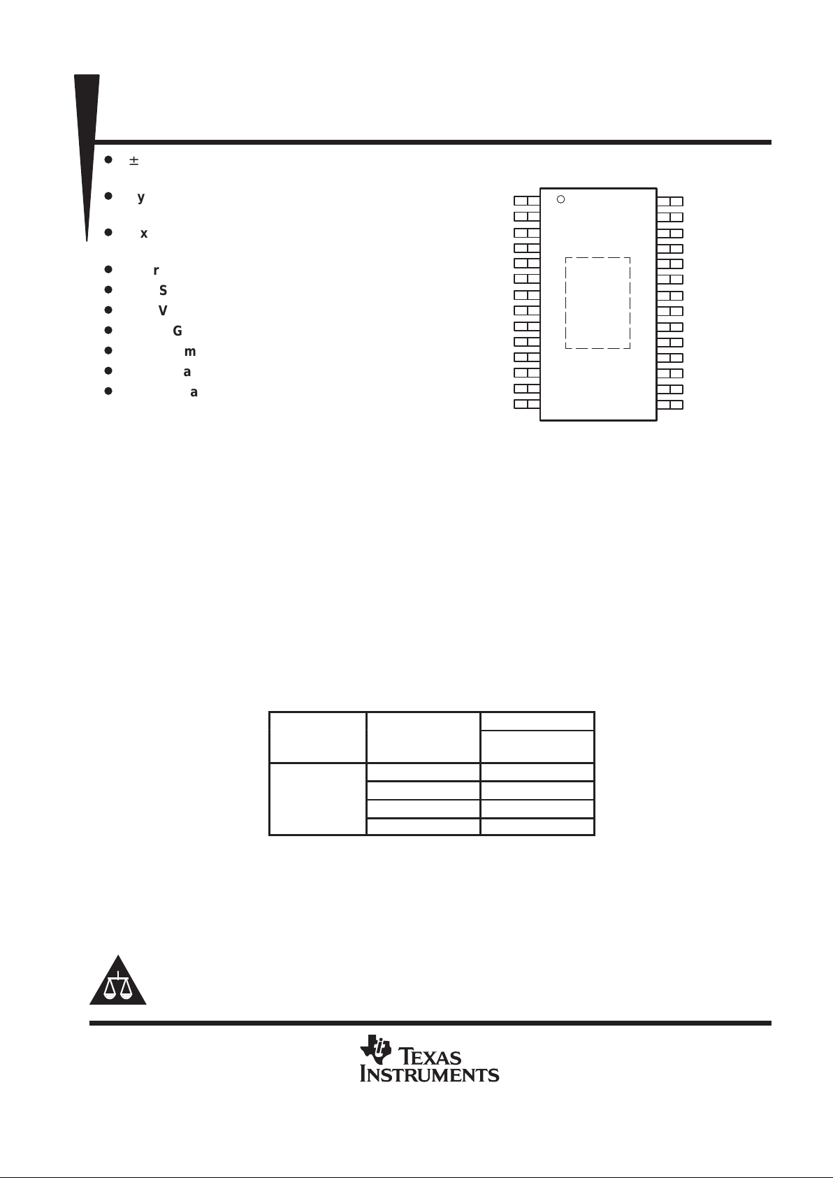
1
2
3
4
5
6
7
8
9
10
11
12
13
14
28
27
26
25
24
23
22
21
20
19
18
17
16
15
IOUT
AGND2
OCP
VHYST
VREFB
VSENSE
ANAGND
SLOWST
BIAS
LODRV
LOHIB
DRVGND
LOWDR
DRV
PWRGD
NC
NC
NC
NC
NC
INHIBIT
IOUTLO
LOSENSE
HISENSE
BOOTLO
HIGHDR
BOOT
V
CC
PWP PACKAGE
(TOP VIEW)
NC – No internal connection
PowerPAD is a trademark of Texas Instruments Incorporated.
TPS5615, TPS5618, TPS5625, TPS5633
SYNCHRONOUS-BUCK HYSTERETIC REGULATOR CONTROLLER
SLVS177A – SEPTEMBER 1998 – REVISED NOVEMBER 1998
2
POST OFFICE BOX 655303 • DALLAS, TEXAS 75265
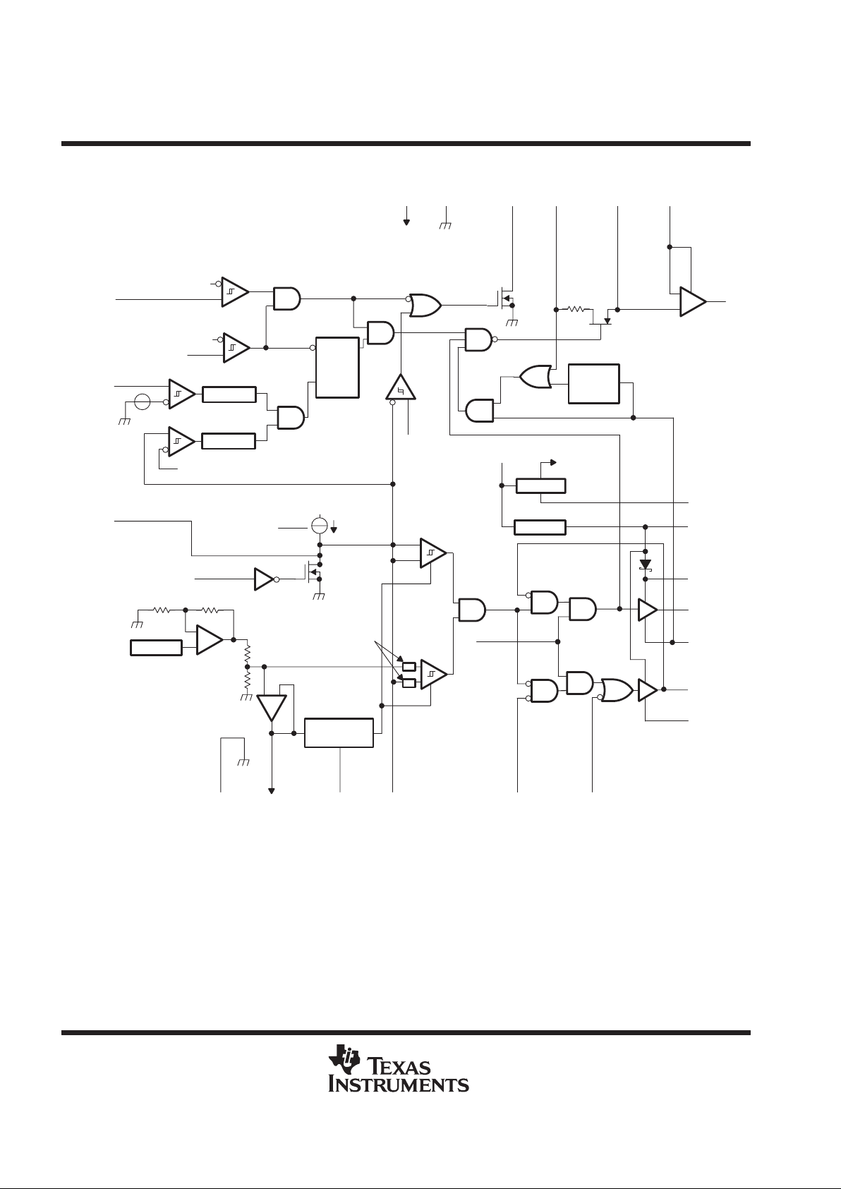
functional block diagram
INHIBIT
OCP
SLOWST
IOUT
BIAS
DRV
BOOT
HIGHDR
BOOTLO
LOWDR
DRVGND
HISENSEIOUTLOLOSENSEPWRGDANAGND
CC
V
VREFBAGND2 VSENSEVHYST LODRVLOHIB
_
+
2 V
10 V
UVLO
V
CC
22
3
8
25 4 6 11 10
15 7 28 20
21
19
1
9
14
16
17
18
13
12
_
+
Deglitch
100mV
VOVP
1.15 VREF
VSENSE
S
R
Q
V
CC
Deglitch
Fault
Shutdown
VPGD
0.93 VREF
Rising
Edge
Delay
HIGHIN
HIGHDR
2X
Shutdown
_
+
Bandgap
_
+
I
VREFB
5
Analog
Bias
VREF
Hysteresis
Setting
I
VREFB
_
+
_
+
Hysteresis
Comparator
Shutdown
Slowstart
Comparator
CM Filters
PREREG
DRV REG
V
CC
Analog
Bias
TPS5615, TPS5618, TPS5625, TPS5633
SYNCHRONOUS-BUCK HYSTERETIC REGULATOR CONTROLLER
SLVS177A – SEPTEMBER 1998 – REVISED NOVEMBER 1998
3
POST OFFICE BOX 655303 • DALLAS, TEXAS 75265
Terminal Functions
TERMINAL
NAME NO.
I/O
DESCRIPTION
AGND2 2 Analog ground (must be connected).
ANAGND 7 Analog ground
BIAS 9 Analog bias pin. A 1-µF capacitor should be connected from BIAS to ANAGND.
BOOT 16 Bootstrap. A 1-µF capacitor should be connected from BOOT to BOOTLO.
BOOTLO 18 Bootstrap low. Connect to the junction of the high-side and low-side FETs for floating drive configuration.
Connect to PGND for ground-reference drive configuration.
DRV 14 Drive regulator for the FET drivers. A 1-µF capacitor should be connected from DRV to DRVGND.
DRVGND 12 Drive ground. Ground for FET drivers. Connect to FET PWRGND.
HIGHDR 17 High drive. Output drive to high-side power switching FETs.
HISENSE 19 High current sense. For current sensing across high-side FET s, connect to the drain of the high-side FETs;
for optional current sensing scheme, connect to power supply side of current-sense resistor placed in series
with high-side FET drain.
INHIBIT 22 Disables the drive signals to the MOSFET drivers. Also serves as UVLO for system logic supply (3.3 V or
5 V). An external pull-up resistor should be connected to system-logic supply.
IOUT 1 Current out. Output voltage on this terminal is proportional to the load current as measured across the
R
ds(on)
of the high side FET . The voltage on this terminal equals 2 ×R
DS(ON)
×IOUT . In applications where
very accurate current-sensing is required, a sense resistor should be connected between the input supply
and the drain of the high-side FETs.
IOUTLO 21 Current sense low output. This is the voltage on the LOSENSE terminal when the high-side FETs are on.
A ceramic capacitor (between 0.033 µF and 0.1 µF) should be connected from IOUTLO to HISENSE to hold
the sensed voltage.
LODRV 10 Low drive enable. Normally tied to 5 V. To configure the low-side FET as a crowbar , pull LODRV low.
LOHIB 11 Low side inhibit. Connect to the junction of the high- and low-side FETs to control the anti-cross-
conduction and eliminate shoot-through current. Disabled when configured in crowbar mode.
LOSENSE 20 Low current sense. For current sensing across high-side FET s, connect to the source of the high-side FET s;
for optional current sensing scheme, connect to high-side FET drain side of current-sense resistor placed
in series with high-side FET drain.
LOWDR 13 Low drive. Output drive to synchronous rectifier FETs.
NC 23–27 No connect
OCP 3 Over current protection. Current limit trip point is set with a resistor divider between IOUT and ANAGND.
PWRGD 28 Power good. PWRGD signal goes high when output voltage is within 7% of voltage setpoint. Open-drain
output.
SLOWST 8 Slow Start (soft start). A capacitor form SLOWST to ANAGND sets the slowstart time.
Slowstart current = I
VREFB
/5
VHYST 4 Hysteresis set input. The hysteresis is set with a resistor divider from VREFB to ANAGND.
Hysteresis = 2 × (VREFB – VHYST)
V
CC
15 12-V supply. A 1-µF capacitor should be connected from VCC to DRVGND.
VREFB 5 Buffered reference voltage
VSENSE 6 Voltage sense Input. T o be connected from converter output voltage bus to sense and control output voltage.
It is recommended that a RC low-pass filter be connected at this pin to filter noise.
TPS5615, TPS5618, TPS5625, TPS5633
SYNCHRONOUS-BUCK HYSTERETIC REGULATOR CONTROLLER
SLVS177A – SEPTEMBER 1998 – REVISED NOVEMBER 1998
4
POST OFFICE BOX 655303 • DALLAS, TEXAS 75265
detailed description
Vref
The reference voltage section consists of a temperature-compensated bandgap reference and a resistive
divider that sets the output voltage option. The output voltage, VREF, is within 1% of the nominal setting over
the full junction temperature range of 0°C to 125°C, and a V
CC
supply voltage range of 11.4 V to 12.6 V. The
output of the reference network is indirectly brought out through a buffer to the VREFB pin. The voltage on this
pin will be within 2% of VREF . It is not recommended to drive loads with VREFB, other than setting the hysteresis
of the hysteretic comparator, because the current drawn from VREFB sets the charging current for the slowstart
capacitor. Refer to the
slowstart
section for additional information.
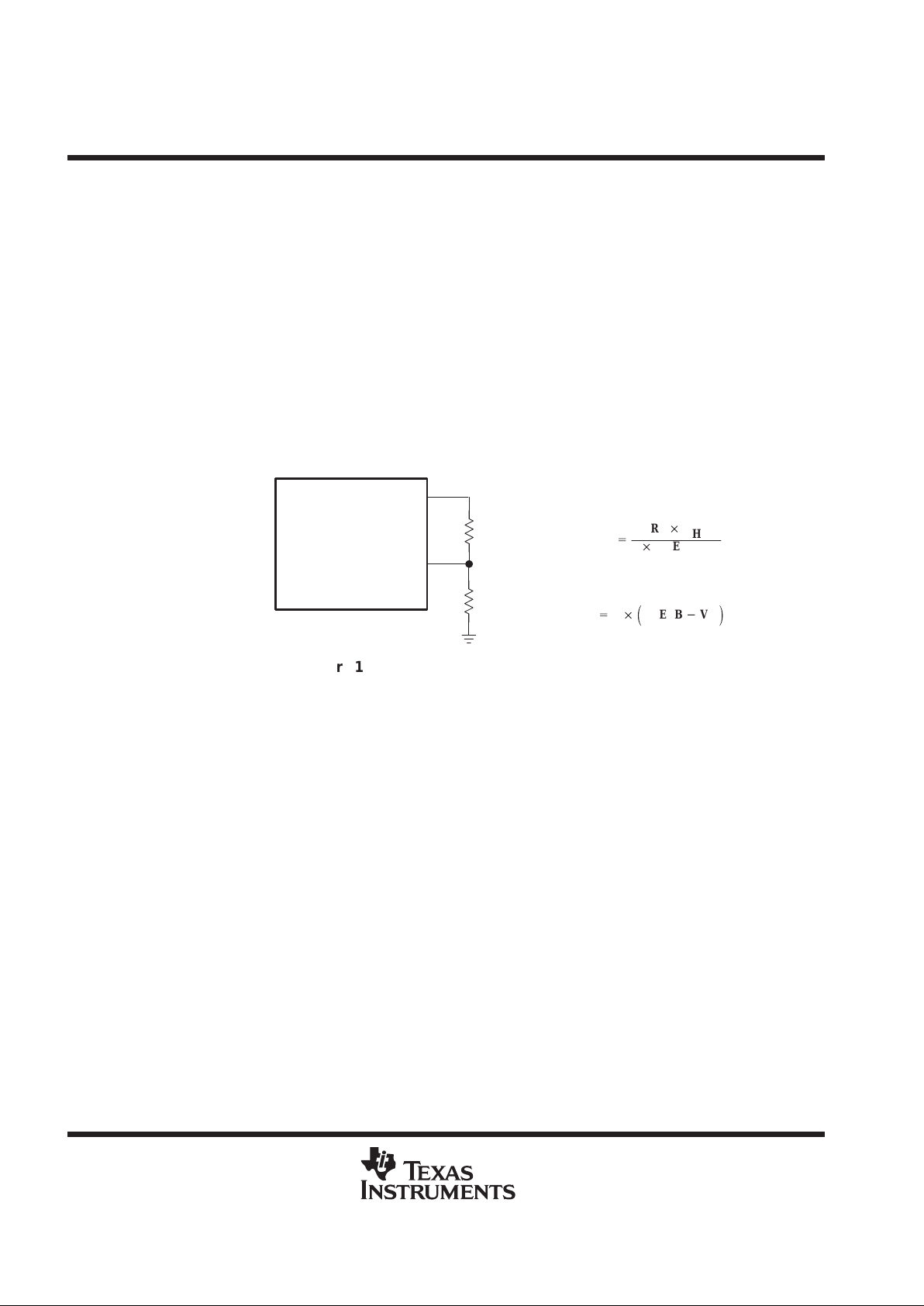
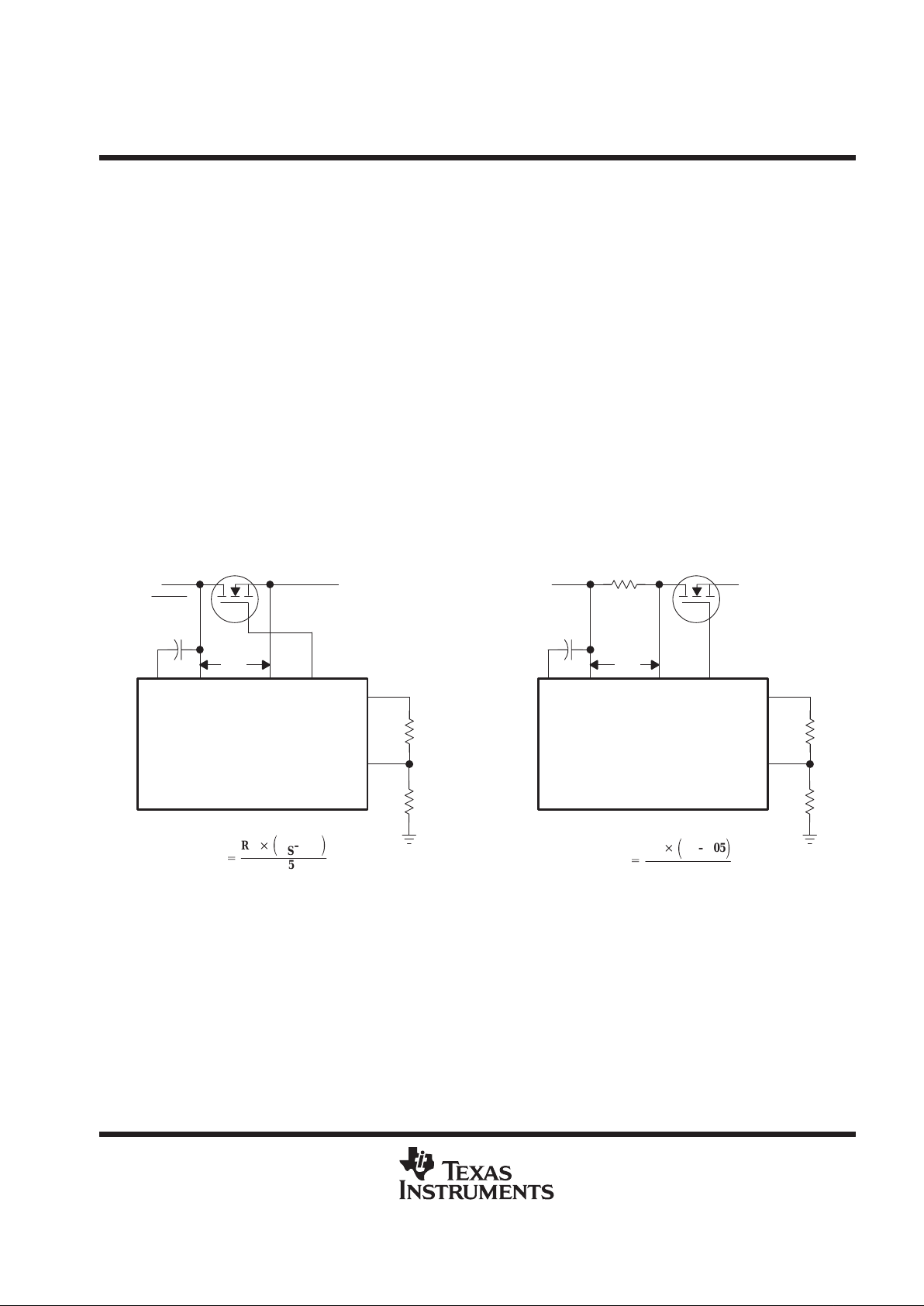
hysteretic comparator
The hysteretic comparator regulates the output voltage of the synchronous-buck converter. The hysteresis is
set by 2 external resistors and is centered on VREF . The 2 external resistors form a resistor divider from VREFB
to ANAGND, with the output voltage connecting to the VHYST pin. The hysteresis of the propagation delay from
the comparator inputs to the driver outputs is 250 ns (maximum). The maximum hysteresis setting is 60 mV.
R1
+
R2 V
H
2 VREFB–V
H
Where
VH =
desired hysteresis voltage
I
O(MAX)
= 0.5 µA
VHYST
TPS56xx
VREFB
R1
R2
+2 ǒVREFB*V
H
Ǔ
Figure 1. Setting the Hysteresis Voltage
low-side driver
The low-side driver is designed to drive low-R
ds(on)
n-channel MOSFETs. The current rating of the driver is 2
A, source or sink. The bias to the low-side driver is internally connected to the DRV regulator.
high-side driver
The high-side driver is designed to drive low-R
ds(on)
n-channel MOSFETs. The current rating of the driver is 2
A, source or sink. The high-side driver can be configured either as a ground-referenced driver or as a floating
bootstrap driver. When configured as a floating driver , the bias voltage to the driver is developed from the DR V
regulator. The internal bootstrap diode, connected between the DR V and BOOT pins, is a Schottky for improved
drive efficiency. The maximum voltage that can be applied between BOOT and DRVGND is 30 V. The driver
can be referenced to ground by connecting BOOTLO to DRVGND, and connecting BOOT to either DRV or V
CC
.
deadtime control
Deadtime control prevents shoot-through current from flowing through the main power FETs during switching
transitions by actively controlling the turn-on times of the MOSFET drivers. The high-side driver is not allowed
to turn on until the gate-drive voltage to the low-side FET is below 2 V; the low-side driver is not allowed to turn
on until the voltage at the junction of the 2 FETs (Vphase) is below 2 V.
TPS5615, TPS5618, TPS5625, TPS5633
SYNCHRONOUS-BUCK HYSTERETIC REGULATOR CONTROLLER
SLVS177A – SEPTEMBER 1998 – REVISED NOVEMBER 1998
5
POST OFFICE BOX 655303 • DALLAS, TEXAS 75265
detailed description (continued)
current sensing
Current sensing is achieved by sampling and holding the voltage across the high-side power FET while the
high-side FET is on. The sampling network consists of an internal 60-Ω switch and an external ceramic hold
capacitor. Recommended value of the hold capacitor is between 0.033 µ F and 0.1 µF. The actual value should
give a time constant (60 Ω × C
H
) greater than the FET on time. Internal logic controls the turn-on and turn-off
of the sample/hold switch such that the switch does not turn on until the Vphase voltage transitions high, and
the switch turns off when the input to the high-side driver goes low . Thus sampling will occur only when the high
side FET is conducting current. The voltage on the IOUT pin equals 2 times the sensed high-side voltage. In
applications where a higher accuracy in current-sensing is required, a sense resistor can be placed in series
with the high-side FET and the voltage across the sense resistor can be sampled by the current sensing circuit.
See Figures 2 and 3.
overcurrent protection
The overcurrent protection (OCP) circuit monitors the current through the high-side FET. The overcurrent
threshold is adjustable with an external resistor divider between IOUT and ANAGND, with the divider voltage
connected to OCP. If the voltage on OCP (V
S
) exceeds 100 mV , then a fault latch is set and the output drivers
are turned off. The latch will remain set until V
CC
goes below the undervoltage lockout value. A 3-µs deglitch
timer is included for noise immunity . The OCP circuit is also designed to protect the high-side power FET against
a short-to-ground fault on the terminal common to both power FETs (Vphase).
R1
+
R2
ǒ
VS–0.05
Ǔ
0.05
Figure 2. OCP Using FET ON-Resistance
Figure 3. Precision OCP Using External Resistor
R1
+
R2
ǒ
VS–0.05
Ǔ
0.05
R2
2 * V
S
OCP
TPS56xx
R1
IOUT
IOUTLO
HISENSE
LOSENSE
HIGHDR
V
CC
V
P
C
H
V
S
R2
2 * V
S
OCP
TPS56xx
R1
IOUT
IOUTLO
HISENSE
LOSENSE
HIGHDR
V
CC
V
P
C
H
V
S
R
S
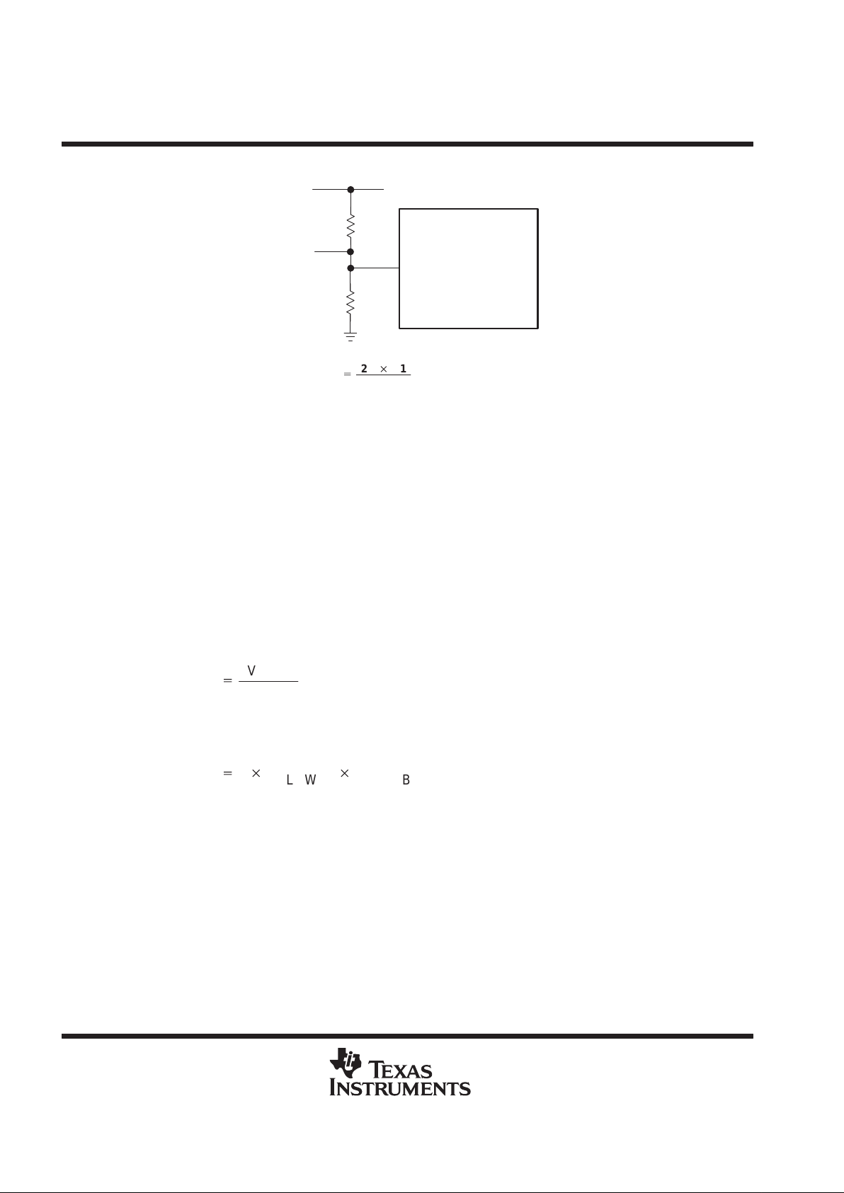
inhibit
INHIBIT is a TTL-compatible digital input used to enable the controller. When INHIBIT is low , the output drivers
are low and the slowstart capacitor is discharged. When INHIBIT goes high, the short across the slowstart
capacitor is released and normal converter operation begins. When the system-logic supply is connected to
INHIBIT, it also controls power sequencing by locking out controller operation until the system-logic supply
exceeds the input threshold voltage of the inhibit circuit. Thus the 12-V supply and the system-logic supply
(either 5 V or 3.3 V) must be above UVLO thresholds before the controller is allowed to start up. The INHIBIT
comparator start threshold is 2.1 V and the hysteresis is 100 mV.
TPS5615, TPS5618, TPS5625, TPS5633
SYNCHRONOUS-BUCK HYSTERETIC REGULATOR CONTROLLER
SLVS177A – SEPTEMBER 1998 – REVISED NOVEMBER 1998
6
POST OFFICE BOX 655303 • DALLAS, TEXAS 75265
detailed description (continued)
R2
+
2.1 R1
V
TRIP
–2.1
Where
V
TRIP
=desired V
SUPPLY
trip voltage
R2
INHIBIT
TPS56xx
R1
To Power Stage
SHUTDOWN
V
CC
Figure 4. Input Undervoltage Lockout Circuit Using INHIBIT
V
CC
undervoltage lockout (UVLO)
The undervoltage lockout circuit disables the controller while the V
CC
supply is below the 10-V start threshold
during power-up. While the controller is disabled, the output drivers will be low and the slowstart capacitor will
be shorted. When V
CC
exceeds the start threshold, the short across the slowstart capacitor is released and
normal converter operation begins. There is a 2-V hysteresis in the undervoltage lockout circuit for noise
immunity.
slowstart
The slowstart circuit controls the rate at which V
O
powers up. A capacitor is connected between SLOWSST and
ANAGND and is charged by an internal current source. The slowstart charging current is determined by the
following equation:
I
SLOWSTART
+
I(VREFB)
5
where I(VREFB) is the current flowing out of VREFB. It is recommended that no additional loads be connected
to VREFB, other than the resistor divider for setting the hysteresis voltage. The maximum current that can be
sourced by the VREFB circuit is 500 µA. The slowstart time is set by:
t
SLOWSTART
+5
C
SLOWST
R
VREFB
where R
VREFB
is the total external resistance from VREFB to ANAGND.
power good
The power good circuit monitors for an undervoltage condition on V
O
. If VO is 7% below V
REF
, then PWRGD
is pulled low. PWRGD is an open-drain output.
overvoltage protection
The overvoltage protection (OVP) circuit monitors V
O
for an overvoltage condition. If VO is 15% above V
REF
,
then a fault latch is set and both output drivers are turned off. The latch will remain set until V
CC
goes below the
undervoltage lockout value. A 3-µs deglitch timer is included for noise immunity. Refer to the LODRV section
for information on how to protect the load against overvoltages due to a shorted fault across the high-side power
FET .
TPS5615, TPS5618, TPS5625, TPS5633
SYNCHRONOUS-BUCK HYSTERETIC REGULATOR CONTROLLER
SLVS177A – SEPTEMBER 1998 – REVISED NOVEMBER 1998
7
POST OFFICE BOX 655303 • DALLAS, TEXAS 75265
detailed description (continued)
drive regulator
The drive regulator provides drive voltage to the output drivers. The minimum drive voltage is 7 V . The minimum
short circuit current is 100 mA. Connect a 1-µF ceramic capacitor from DRV to DRVGND.
LODRV
The LODRV circuit is designed to protect the load against overvoltages that occur if the high-side FET s become
shorted. External components to sense an overvoltage condition are required to use this feature. When an
overvoltage fault occurs, LODRV is pulled low and the low-side FET will be turned on, overriding all control
signals inside the TPS56xx controller. The crowbar action will short the system-logic supply to ground through
the faulted high-side FET s and the low-side FETs. A fuse, in series with V
IN
, should be added to disconnect the
short circuit.
absolute maximum ratings over operating free-air temperature (unless otherwise noted)
†
Supply voltage range, V
CC
(see Note 1) –0.3 to 14 V. . . . . . . . . . . . . . . . . . . . . . . . . . . . . . . . . . . . . . . . . . . . . . .
Input voltage range: BOOT to DRVGND (high-side driver ON) –0.3 to 30 V. . . . . . . . . . . . . . . . . . . . . . . . . . .
BOOT to HIGHDRV –0.3 to 15 V. . . . . . . . . . . . . . . . . . . . . . . . . . . . . . . . . . . . . . . . . . . . . .
BOOT to BOOTLO –0.3 to 15 V. . . . . . . . . . . . . . . . . . . . . . . . . . . . . . . . . . . . . . . . . . . . . . .
INHIBIT, LODRV –0.3 to 7.3 V. . . . . . . . . . . . . . . . . . . . . . . . . . . . . . . . . . . . . . . . . . . . . . . . .
PWRGD, OCP –0.3 to 7 V. . . . . . . . . . . . . . . . . . . . . . . . . . . . . . . . . . . . . . . . . . . . . . . . . . .
LOHIB, LOSENSE, IOUTLO, HISENSE –0.3 to 14 V. . . . . . . . . . . . . . . . . . . . . . . . . . . .
VSENSE –0.3 to 5 V. . . . . . . . . . . . . . . . . . . . . . . . . . . . . . . . . . . . . . . . . . . . . . . . . . . . . . . .
Voltage difference between ANAGND and DRVGND ±0.5 V. . . . . . . . . . . . . . . . . . . . . . . . . . . . . . . . . . . . . . . . .
Output current, VREFB 0.5 mA. . . . . . . . . . . . . . . . . . . . . . . . . . . . . . . . . . . . . . . . . . . . . . . . . . . . . . . . . . . . . . . . . . .
Short circuit duration, DRV Continuous. . . . . . . . . . . . . . . . . . . . . . . . . . . . . . . . . . . . . . . . . . . . . . . . . . . . . . . . . . . .
Continuous total power dissipation See Dissipation Rating Table. . . . . . . . . . . . . . . . . . . . . . . . . . . . . . . . . . . . .
Operating junction temperature range, T
J
0°C to 125°C. . . . . . . . . . . . . . . . . . . . . . . . . . . . . . . . . . . . . . . . . . . . .
Storage temperature range, T
stg
–65°C to 150°C. . . . . . . . . . . . . . . . . . . . . . . . . . . . . . . . . . . . . . . . . . . . . . . . . . .
Lead temperature soldering 1,6 mm (1/16 inch) from case for 10 seconds 260°C. . . . . . . . . . . . . . . . . . . . . . .
†
Stresses beyond those listed under “absolute maximum ratings” may cause permanent damage to the device. These are stress ratings only, and
functional operation of the device at these or any other conditions beyond those indicated under “recommended operating conditions” is not
implied. Exposure to absolute-maximum-rated conditions for extended periods may affect device reliability.
NOTE 1: Unless otherwise specified, all voltages are with respect to ANAGND.
DISSIPATION RATING TABLE
PACKAGE
TA ≤ 25°C
POWER RATING
DERATING FACTOR
ABOVE TA = 25°C
TA = 70°C
POWER RATING
TA = 85°C
POWER RATING
PWP 1150 mW 11.5 mW/°C 630 mW 460 mW
TPS5615, TPS5618, TPS5625, TPS5633
SYNCHRONOUS-BUCK HYSTERETIC REGULATOR CONTROLLER
SLVS177A – SEPTEMBER 1998 – REVISED NOVEMBER 1998
8
POST OFFICE BOX 655303 • DALLAS, TEXAS 75265
recommended operating conditions
MIN MAX UNIT
Supply voltage, V
CC
11.4 13 V
BOOT to DRVGND 0 28
BOOT to BOOTLO 0 13
Input voltage
INHIBIT, LODRV, PWRGD, OCP 0 6
V
LOHIB, LOSENSE, IOUTLO, HISENSE 0 13
VSENSE 0 4.5
Voltage dif ference between ANAGND and DRVGND 0 ±0.2 V
Output current, VREFB
†
0 0.4 mA
†
Not recommended to load VREFB other than to set hysteresis since I
VREFB
sets slowstart time.
electrical characteristics over recommended operating virtual junction temperature range,
V
CC
= 12 V, I
DRV
= 0 A (unless otherwise noted)
reference
PARAMETER TEST CONDITIONS MIN TYP MAX UNIT
TPS5615 1.485 1.515
Reference
TPS5618
1.782 1.818
VREF
Reference
voltage
TPS5625
V
CC
=
11.4 V to 12.6 V
2.475 2.525
V
TPS5633 3.267 3.333
VREFB Output voltage I
REFB
= 50 µA VREF–2% VREF VREF+2% V
VREFB Output regulation 10 µA ≤ IO ≤ 500 µA 2 mV
power good
PARAMETER TEST CONDITIONS MIN TYP MAX UNIT
Undervoltage trip threshold 90 93 95 %VREF
Low-level output voltage, PWRGD IO = 5 mA 0.5 0.75 V
High-level input current, PWRGD V
PWRGD
= 6 V 1 µA
Hysteresis 10 mV
overvoltage protection
PARAMETER TEST CONDITIONS MIN TYP MAX UNIT
Overvoltage trip threshold 112 115 120 %VREF
Hysteresis See Note 2 10 mV
NOTE 2: Ensured by design, not tested.
slowstart
PARAMETER TEST CONDITIONS MIN TYP MAX UNIT
Charge current V
SLOWST
= 0.5 V, I
VREFB
= 65 µA 10.4 13 15.6 µA
Discharge current V
SOFTST
= 1 V 3 mA
Comparator input offset voltage 10 mV
Comparator input bias current See Note 2 10 100 nA
Hysteresis –7.5 7.5 mV
NOTE 2: Ensured by design, not tested.

TPS5615, TPS5618, TPS5625, TPS5633
SYNCHRONOUS-BUCK HYSTERETIC REGULATOR CONTROLLER
SLVS177A – SEPTEMBER 1998 – REVISED NOVEMBER 1998
9
POST OFFICE BOX 655303 • DALLAS, TEXAS 75265
electrical characteristics over recommended operating virtual junction temperature range,
V
CC
= 12 V, I
DRV
= 0 A (unless otherwise noted) (continued)
inhibit
PARAMETER TEST CONDITIONS MIN TYP MAX UNIT
Startup threshold 1.9 2.1 2.35 V
Hysteresis 0.08 0.1 0.12 V
Stop threshold 1.85 V
input undervoltage lockout
PARAMETER TEST CONDITIONS MIN TYP MAX UNIT
Startup threshold 9.25 10 10.75 V
Hysteresis 1.9 2 2.2 V
Stop threshold 7.5 V
hysteretic comparator
PARAMETER TEST CONDITIONS MIN TYP MAX UNIT
Input offset voltage –2.5 2.5 mV
Input bias current See Note 2 500 nA
Hysteresis accuracy V
REFB
– V
HYST
= 15 mV, (hysteresis window = 30 mV) –3.5 3.5 mV
Maximum hysteresis setting V
REFB
– V
HYST
= 30 mV 60 mV
NOTE 2: Ensured by design, not tested.
overcurrent protection
PARAMETER TEST CONDITIONS MIN TYP MAX UNIT
OCP trip threshold 90 100 110 mV
Input bias current 100 nA

TPS5615, TPS5618, TPS5625, TPS5633
SYNCHRONOUS-BUCK HYSTERETIC REGULATOR CONTROLLER
SLVS177A – SEPTEMBER 1998 – REVISED NOVEMBER 1998
10
POST OFFICE BOX 655303 • DALLAS, TEXAS 75265
electrical characteristics over recommended operating virtual junction temperature range,
V
CC
= 12 V, I
DRV
= 0 A (unless otherwise noted) (continued)
high-side VDS sensing
PARAMETER TEST CONDITIONS MIN TYP MAX UNIT
Gain 2 V/V
V
HISENSE
= 12 V, V
LOSENSE
= 11.9 V
Initial accuracy
Differential input to Vds sensing amp = 100 mV
194
206
mV
IOUTLO sink current 5 V ≤ V
IOUTLO
≤ 13 V 250 nA
IOUT source current
V
IOUT
= 0.5 V,
V
IOUTLO
= 11.5 V
V
HISENSE
= 12 V,
500 µA
IOUT sink current
V
IOUT
= 0.05 V ,
V
IOUTLO
= 12 V
V
HISENSE
= 12 V,
50 µA
V
HISENSE
= 11 V 0 2
Output voltage swing
V
HISENSE
= 4.5 V
R
IOUT
= 10 kΩ
0 1.5
V
V
HISENSE
= 3 V 0 0.75
LOSENSE high-level input voltage V
HISENSE
= 4.5 V, See Note 2 2.85 V
LOSENSE low-level input voltage V
HISENSE
= 4.5 V, See Note 2 2.4 V
11.4 V ≤ V
HISENSE
≤ 12.6 V,
LOSENSE connected to HISENSE,
V
HISENSE
– V
IOUTLO
= 0.15 V
50 60 80
Sample/hold resistance
4.5 V ≤ V
HISENSE
≤ 5.5 V,
LOSENSE connected to HISENSE,
V
HISENSE
– V
IOUTLO
= 0.15 V
62 85 123
Ω
3 V ≤ V
HISENSE
≤ 3.6 V,
LOSENSE connected to HISENSE,
V
HISENSE
– V
IOUTLO
= 0.15 V
67 95 144
CMRR
V
HISENSE
= 12.6 V to 3 V,
V
HISENSE
– V
OUTLO
= 100 mV
69 75 dB
NOTE 2: Ensured by design, not tested.
deadtime
PARAMETER TEST CONDITIONS MIN TYP MAX UNIT
LOHIB
p
See Note 2 2.4
LODR
High-level input voltage
See Note 2 3
V
LOHIB
p
See Note 2 1.4
LODR
Low-level input voltage
See Note 2 1.7
V
NOTE 2: Ensured by design, not tested.
LODRV
PARAMETER TEST CONDITIONS MIN TYP MAX UNIT
High-level input voltage 1.85 V
LODRV
Low-level input voltage 0.95 V
drive regulator
PARAMETER TEST CONDITIONS MIN TYP MAX UNIT
Output voltage 11.4 V ≤ VCC ≤ 12.6 V, I
DRV
= 50 mA 7 9 V
Output regulation 1 mA ≤ I
DRV
≤ 500 mA 100 mV
Short-circuit current 100 mA

TPS5615, TPS5618, TPS5625, TPS5633
SYNCHRONOUS-BUCK HYSTERETIC REGULATOR CONTROLLER
SLVS177A – SEPTEMBER 1998 – REVISED NOVEMBER 1998
11
POST OFFICE BOX 655303 • DALLAS, TEXAS 75265
electrical characteristics over recommended operating virtual junction temperature range,
V
CC
= 12 V, I
DRV
= 0 A (unless otherwise noted) (continued)
bias regulator
PARAMETER TEST CONDITIONS MIN TYP MAX UNIT
Output voltage 11.4 V ≤ VCC ≤ 12.6 V, See Note 3 6 V
NOTE 3: The bias regulator is designed to provide a quiet bias supply for the TPS56xx controller. External loads should not be driven by the bias
regulator.
output drivers
PARAMETER (see Note 4) TEST CONDITIONS MIN TYP MAX UNIT
High-side sink
Duty cycle < 2%, tpw < 100 µs, TJ = 125°C,
2
p
High-side source
V
BOOT
–
V
BOOTLO
=
6.5 V
,
V
HIGHDR
= 1.5 V (SRC) or 5 V (sink), See Note 2
2
Peak output current
Low-side sink
Duty cycle < 2%, tpw < 100 µs, TJ = 125°C,
2
A
Low-side source
V
DRV
= 6.5 V,
V
LOWDR
= 1.5 V
(SRC)
or 5
V
(sink), See Note 2
2
High-side sink
T
= 125°C, V
– V
= 6.5 V,
3
p
High-side source
J
,
BOOT BOOTLO
,
V
HIGHDR
= 1.5 V (SRC) or 5 V (sink)
45
Output resistance
Low-side sink
TJ = 125°C, V
DRV
= 6.5 V,
5.7
Ω
Low-side source
J DRV
V
LOWDR
= 1.5 V (SRC) or 5 V (sink)
45
NOTES: 2. Ensured by design, not tested.
4. The pull up/down circuits of the drivers are bipolar and MOSFET transistors in parallel. The peak output current rating is the
combined current from the bipolar and MOSFET transistors. The output resistance is the R
DS(ON)
of the MOSFET transistor when
the voltage on the driver output is less than the saturation voltage of the bipolar transistor.
supply current
PARAMETER TEST CONDITIONS MIN TYP MAX UNIT
VCC supply voltage range 11.4 12 13 V
V
INHIBIT
= 5 V,
V
BOOTLO
= 0 V,
VCC > 10.75 V at startup,
See Note 2
3 10
VCC quiescent current
V
INHIBIT
= 5 V,
V
BOOTLO
= 0 V,
C
LOWDR
= 50 pF,
VCC > 10.75 V at startup,
C
HIGHDR
= 50 pF,
f
swx
= 200 kHz
5
mA
V
INHIBIT
= 0 V or VCC < 9.25 V at startup,
V
BOOT
= 13 V, V
BOOTLO
= 0 V
10 µA
High-side drive regulator quiescent current
V
INHIBIT
= 5 V,
V
BOOT
= 13 V,
C
HIGHDR
= 50 pF,
VCC > 10.75 V at startup,
V
BOOTLO
= 0 V,
f
swx
= 200 kHz
2 mA
NOTE 2: Ensured by design, not tested.

TPS5615, TPS5618, TPS5625, TPS5633
SYNCHRONOUS-BUCK HYSTERETIC REGULATOR CONTROLLER
SLVS177A – SEPTEMBER 1998 – REVISED NOVEMBER 1998
12
POST OFFICE BOX 655303 • DALLAS, TEXAS 75265
switching characteristics over recommended operating virtual junction temperature range,
V
CC
= 12 V, I
DRV
= 0 V (unless otherwise noted)
PARAMETER TEST CONDITIONS MIN TYP MAX UNIT
VSENSE to HIGHDR or
LOWDR (excluding deadtime)
Overdrive = 10 mV (see Note 2) 150 250 ns
OCP comparator See Note 2 1
Propagation delay
OVP comparator See Note 2 1
µs
PWRGD comparator See Note 2 1
SLOWST comparator Overdrive = 10 mV (see Note 2) 560 900 ns
HIGHDR output
CL = 9 nF,
V
BOOTLO
= 0 V,
V
BOOT
= 6.5 V,
TJ = 125°C
60
Rise time
LOWDR output
CL = 9 nF,
TJ = 125°C
V
DRV
= 6.5 V,
60
ns
HIGHDR output
CL = 9 nF,
V
BOOTLO
= 0 V,
V
BOOT
= 6.5 V,
TJ = 125°C
60
Fall time
LOWDR output
CL = 9 nF,
TJ = 125°C
V
DRV
= 6.5 V,
60
ns
Deglitch time (includes
p
p
p
OCP See Note 2 2 5
comparator propagation
delay)
OVP See Note 2 2 5
µ
s
V
HISENSE
= 12 V,
V
IOUTLO
pulsed from 12 V to 11.9 V,
100 ns rise/fall times, See Note 2
2
Response time High-side VDS sensing
V
HISENSE
= 4.5 V,
V
IOUTLO
pulsed from 4.5 V to 4.4 V ,
100 ns rise/fall times, See Note 2
3
µs
V
HISENSE
= 3 V,
V
IOUTLO
pulsed from 3 V to 2.9 V ,
100 ns rise/fall times, See Note 2
3
Short-circuit protection risingedge delay
SCP LOSENSE = 0 V, (see Note 2) 300 500 ns
Turn-on/turn-off delay
VDS sensing sample/hold
switch
3 V ≤ V
HISENSE
≤ 11 V,
V
LOSENSE
= V
HISENSE
(see Note 2)
30 100 ns
Crossover delay time
LOWDR to HIGHDRV, and
LOHIB to LOWDR
See Note 2 30 100 ns
Prefilter pole frequency Hysteretic comparator See Note 2 5 MHz
Propagation delay LODRV See Note 2 400 ns
NOTE 2: Ensured by design, not tested.

TPS5615, TPS5618, TPS5625, TPS5633
SYNCHRONOUS-BUCK HYSTERETIC REGULATOR CONTROLLER
SLVS177A – SEPTEMBER 1998 – REVISED NOVEMBER 1998
13
POST OFFICE BOX 655303 • DALLAS, TEXAS 75265
TYPICAL CHARACTERISTICS
Figure 5
SLOWSTART TIMING
vs
CAPACITANCE
0.1
0.0001 0.001 0.01 0.1
0
SLOWSTART T ime – ms
Capacitance – µF
1
100
10
V
REFB
= 2 V
I
(VREFB)
= 100µA
C
(SLOWST)
= 0.1 µF
TJ = 25°C
1
Figure 6
SLOWSTART TIMING
vs
VREFB CURRENT
1 10 100
1
SLOWSTART T iming – ms
I
(VREFB)
– VREFB Current – µA
1000
1000
100
V
REFB
= 2 V
C
(SLOWST)
= 0.1µF
TJ = 25°C
10
Figure 7
OUTPUT DRIVER RISE TIME
vs
LOAD CAPACITANCE
0.1 1 10
1
CL – Load Capacitance – nF
100
100
10
High Side Driver
Low Side Driver
t
r
– Output Driver Rise Time – ns
Figure 8
OUTPUT DRIVER FALL TIME
vs
LOAD CAPACITANCE
0.1 1 10
1
CL – Load Capacitance – nF
100
1000
100
High Side Driver
10
Low Side Driver
t
f
– Output Driver Fall Time – ns

TPS5615, TPS5618, TPS5625, TPS5633
SYNCHRONOUS-BUCK HYSTERETIC REGULATOR CONTROLLER
SLVS177A – SEPTEMBER 1998 – REVISED NOVEMBER 1998
14
POST OFFICE BOX 655303 • DALLAS, TEXAS 75265
TYPICAL CHARACTERISTICS
Figure 9
OVP THRESHOLD VOLTAGE
vs
JUNCTION TEMPERATURE
0255075
100 125
TJ – Junction Temperature – °C
115
114
OVP Threshold V oltage – %
117
118
112
116
113
Figure 10
OCP THRESHOLD VOLTAGE
vs
JUNCTION TEMPERATURE
0255075
100 125
TJ – Junction Temperature – °C
99
97
OCP Threshold V oltage – mV
103
105
95
101
Figure 11
INHIBIT START THRESHOLD VOLTAGE
vs
JUNCTION TEMPERATURE
0255075
100 125
TJ – Junction Temperature – °C
1.95
INHIBIT Start Threshold Voltage – V
2.05
2.1
1.90
2
Figure 12
INHIBIT HYSTERESIS VOLTAGE
vs
JUNCTION TEMPERATURE
0255075
100 125
TJ – Junction Temperature – °C
75
INHIBIT Hysteresis Voltage – mV
125
150
50
100

TPS5615, TPS5618, TPS5625, TPS5633
SYNCHRONOUS-BUCK HYSTERETIC REGULATOR CONTROLLER
SLVS177A – SEPTEMBER 1998 – REVISED NOVEMBER 1998
15
POST OFFICE BOX 655303 • DALLAS, TEXAS 75265
TYPICAL CHARACTERISTICS
Figure 13
UVLO START THRESHOLD VOLTAGE V
CC
vs
JUNCTION TEMPERATURE
0255075
100 125
TJ – Junction Temperature – °C
10
10.5
9
9.5
V
CC
UVLO Start Threshold Voltage (
) – V
Figure 14
UVLO HYSTERESIS VOLTAGE (VCC)
vs
JUNCTION TEMPERATURE
0255075
100 125
TJ – Junction Temperature – °C
1.9
1.7
2.3
2.5
1.5
2.1
V
CC
UVLO Hysteresis Voltage (
) – V
Figure 15
QUIESCENT CURRENT V
CC
vs
JUNCTION TEMPERATURE
0255075
100 125
TJ – Junction Temperature – °C
4
6
0
2
V
CC
Quiescent Current (
) – mA
Figure 16
PWRGD THRESHOLD VOLTAGE
vs
JUNCTION TEMPERATURE
0255075
100 125
TJ – Junction Temperature – °C
92
91
94
95
90
93
V
o
PWRGD Threshold Voltage – %

TPS5615, TPS5618, TPS5625, TPS5633
SYNCHRONOUS-BUCK HYSTERETIC REGULATOR CONTROLLER
SLVS177A – SEPTEMBER 1998 – REVISED NOVEMBER 1998
16
POST OFFICE BOX 655303 • DALLAS, TEXAS 75265
TYPICAL CHARACTERISTICS
Figure 17
SLOWSTART CHARGE CURRENT
vs
JUNCTION TEMPERATURE
0255075
100 125
TJ – Junction Temperature – °C
12
11
14
15
10
13
Slowstart Charge Current – Aµ
Figure 18
VDS SAMPLE/HOLD RESISTANCE
vs
JUNCTION TEMPERATURE
0255075
100 125
TJ – Junction Temperature – °C
25
75
100
0
50
VDS Sample/Hold Resistance – Ω
Figure 19
DRIVE REGULATOR OUTPUT VOLTAGE
vs
JUNCTION TEMPERATURE
0255075
100 125
TJ – Junction Temperature – °C
7.75
8.25
8.5
7.5
8
V
o
– Drive Regulator Output Voltage – V
Figure 20
DRIVE REGULATOR LOAD REGULATION
vs
JUNCTION TEMPERATURE
0255075
100 125
TJ – Junction Temperature – °C
150
175
100
125
Drive Regulator Load Regulation – mV

TPS5615, TPS5618, TPS5625, TPS5633
SYNCHRONOUS-BUCK HYSTERETIC REGULATOR CONTROLLER
SLVS177A – SEPTEMBER 1998 – REVISED NOVEMBER 1998
17
POST OFFICE BOX 655303 • DALLAS, TEXAS 75265
TYPICAL CHARACTERISTICS
Figure 21
DRIVE REGULATOR LINE REGULATION
vs
JUNCTION TEMPERATURE
0255075
100 125
TJ – Junction Temperature – °C
150
175
100
125
Drive Regulator Line Regulation – mV
Figure 22
HIGH–SIDE DRIVER OUTPUT RESISTANCE
vs
JUNCTION TEMPERATURE
0255075
100 125
TJ – Junction Temperature – °C
2
1
4
5
0
3
High–Side Driver Output Resistance –
Ω
Figure 23
LOW–SIDE DRIVER OUTPUT RESISTANCE
vs
JUNCTION TEMPERATURE
0255075
100 125
TJ – Junction Temperature – °C
3
2
5
6
0
4
1
Low–Side Driver Output Resistance –
Ω

TPS5615, TPS5618, TPS5625, TPS5633
SYNCHRONOUS-BUCK HYSTERETIC REGULATOR CONTROLLER
SLVS177A – SEPTEMBER 1998 – REVISED NOVEMBER 1998
18
POST OFFICE BOX 655303 • DALLAS, TEXAS 75265
APPLICATION INFORMATION
Synchronous rectifier buck regulator circuits are used where high efficiency and low dropout voltages are required.
The TPS56xx controller is useful in applications with very high transient loads and wide dc load ranges, such as
multiple-DSP applications.
The circuit below will meet a wide variety of applications with maximum continuous-rated output currents of up to 8 A.
Design tradeoffs, such as cost, size, or efficiency may need to be addressed for specific applications. Care should
be taken in the proper layout (see last section of this data sheet for specific layout guidelines), especially in the
higher-current configurations, to ensure that noise and ripple are kept to a minimum. Basic layout considerations are
discussed in the
1996 Power Supply Circuits Databook
(Literature no. SL VD002). Design guidelines and equations
are discussed in
Synchronous Buck Converter Design Using TPS56xx Controllers in SLVP10x EVMs User’s Guide
(Literature no. SLVU007).

TPS5615, TPS5618, TPS5625, TPS5633
SYNCHRONOUS-BUCK HYSTERETIC REGULATOR CONTROLLER
SLVS177A – SEPTEMBER 1998 – REVISED NOVEMBER 1998
19
POST OFFICE BOX 655303 • DALLAS, TEXAS 75265
APPLICATION INFORMATION
IOUT
AGND2
OCP
VHYST
VREFB
VSENSE
ANAGND
SLOWST
BIAS
LODRV
LOHIB
DRVGND
LOWDR
DRV
PWRGD
NC
NC
NC
NC
NC
INHIBIT
IOUTLO
LOSENSE
HISENSE
BOOTLO
HIGHDR
BOOT
VCC
28
27
26
25
24
23
22
21
20
19
18
17
16
15
1
2
3
4
5
6
7
8
9
10
11
12
13
14
C7 1 µF
R4
10 Ω
C11
1 µF
R3
10 Ω
C4
1 µF
C3 0.1 µF
R8
100 Ω
1%
C17 1 µF
C16 0.1 µF
R13
C15 1000 pF
Q2
Si4410
R2
10 kΩ
L1
2.2 µH
C2
0.1 µF
R1
1.0 kΩ
U1
TPS5625
R12
20.0 kΩ 1%
R9
100 Ω 1%
C12 0.1 µF
R6
1.3 kΩ
R11
750 Ω
C14
0.01 µF
R7
11.0 kΩ 1%
R16
4.7 Ω
C1
22 µF
10 V
C5 2.2 µF
C6 680 µF 6.3 V
Q1
Si4410
C8 0.01 µF
C9 820 µF 4V
C10 10 µF
R15
4.7 Ω
J1–1
J1–3
J1–8
J1–7
SD
PG
PwrGND
+12 V
J1–10
J1–9
RETURN
J1–6
J1–5
Vin
J1–18
J1–17
J1–16
J1–15
VsenseL/
8 A
2.5 V
VsenseH
J1–14
J1–13
J1–12
J1–11
PwrGND
J1–2
J1–4
Analog GND
L1 = 10T #22 on T30–18 Core
L2 = 12T #20 on T44–8Core
Not Used:
R10, R13, R14
C13
Power GND
AnaGND
L2
2.6 µH
R5
2.7 Ω
C18
0.1 µF
See Note A
NOTE A: Theses two traces should be physically close to each other for good noise immunity.
R17
1 MΩ
Figure 24. Typical Design Schematic

TPS5615, TPS5618, TPS5625, TPS5633
SYNCHRONOUS-BUCK HYSTERETIC REGULATOR CONTROLLER
SLVS177A – SEPTEMBER 1998 – REVISED NOVEMBER 1998
20
POST OFFICE BOX 655303 • DALLAS, TEXAS 75265
Table 1. Test Results for 2.5-V, 8-A Converter
TEST CONDITIONS QTY UNITS
Output voltage VIN = 5.25 V , IO = 8 A 2.50 V
Load regulation VIN = 5.25 V , IO = 0.8 to 8 A 0.4 %
Line regulation IO =6 A, VCC = 4.5 V to 6 V 0.2 %
Ripple VIN = 5.25 V , IO = 8 A 50 mVpp
Efficiency VIN = 5.25 V , IO = 8 A 89 %
Table 2. 2.5-V, 8-A Converter Bill of Materials
REF DES QTY PART NUMBER DESCRIPTION MFG
C1 1 10SS22M Capacitor , Os-Con, 22 µF, 10 V, 20% Sanyo
C2 4 GRM39X7R104K016A Capacitor , Ceramic, 0.1 µF, 16 V , 10%, X7R muRata
C3 GRM39X7R104K016A Capacitor, Ceramic, 0.1 µF, 16 V, 10%, X7R muRata
C4 4 GRM42-6Y5V105Z016A Capacitor, Ceramic, 1 µF, 16 V, +80%–20% muRata
C5 1 GRM42-6Y5V225Z016A Capacitor, Os-Con, 2.2 µF, 16 V, Y5U muRata
C6 1 6SP680M Capacitor , Os-Con, 680 µF, 6.3 V , 20% Sanyo
C7 GRM42-6Y5V105Z016A Capacitor, Ceramic, 1 µF, 16 V, +80%–20% muRata
C8 2 GRM39X7R103K025A Capacitor , Ceramic, 0.01 µF, 25 V , 10%, X7R muRata
C9 1 4SP820M Capacitor , Os-Con, 820 µF, 4 V , 20% Sanyo
C10 1 GRM235Y5V106Z016A Capacitor, Ceramic, 10 µF, 16 V, Y5V muRata
C11 GRM42-6Y5V105Z016A Capacitor, Ceramic, 1 µF, 16 V, +80%–20% muRata
C12 GRM39X7R104K016A Capacitor, Ceramic, 0.1 µF, 16 V, 10%, X7R muRata
C14 GRM39X7R103K025A Capacitor, Ceramic, 0.01 µF, 25 V, 10%, X7R muRata
C15 1 GRM39X7R102K050A Capacitor, Ceramic, 1000 pF, 50 V, 10%, X7R muRata
C16 GRM39X7R104K016A Capacitor, Ceramic, 0.1 µF, 16 V, 10%, X7R muRata
C17 GRM42-6Y5V105Z016A Capacitor, Ceramic, 1 µF, 16 V, +80%–20% muRata
C18 GRM39X7R104K016A Capacitor, Ceramic, 0.1 µF, 16 V, 10%, X7R muRata
J1 1 S1122-18-ND Header, RA, 18-pin, 0.23 Posts × 0.20 Tails Sullins
L1 1 Inductor, Filter, 2.2 µH, 8.5 A (10T #22 on T30-18 Core)
L2 1 Inductor, Filter, 2.6 µH, 8.5 A (12T #20 on T44-8 Core)
Q1 2 Si4410DY FET, N-ch, 30-V, 10-A, 13-mΩ Siliconix
Q2 Si4410DY FET, N-ch, 30-V, 10-A, 13-mΩ Siliconix
R1 3 Std Resistor, Chip, 1.0 kΩ, 1/16W, 5%
R2 1 Std Resistor, Chip, 10 kΩ, 1/16W, 5%
R3 2 Std Resistor, Chip, 10 Ω, 1/10W, 5%
R4 Std Resistor, Chip, 10 Ω, 1/10W, 5%
R5 1 Std Resistor, Chip, 2.7 Ω, 1/4W, 5%
R6 Std Resistor, Chip, 1.3 kΩ, 1/16W, 5%
R7 1 Std Resistor, Chip, 11.0 kΩ, 1/16W, 1%
R8 2 Std Resistor, Chip, 100 Ω, 1/16W, 1%
R9 Std Resistor, Chip, 100 Ω, 1/16W, 1%
R11 Std Resistor, Chip, 750 Ω, 1/16W, 5%
R12 1 Std Resistor, Chip, 20.0 kΩ, 1/16W, 1%
R15 2 Std Resistor, Chip, 4.7 Ω, 1/16W, 5%
R16 Std Resistor, Chip, 4.7 Ω, 1/16W, 5%
R17 1 Std Resistor, Chip, 1 MΩ, 1/16W, 5%
U1 1 TPS5625PWP IC, PWM Ripple Controller, FIxed 2.5 V TI

TPS5615, TPS5618, TPS5625, TPS5633
SYNCHRONOUS-BUCK HYSTERETIC REGULATOR CONTROLLER
SLVS177A – SEPTEMBER 1998 – REVISED NOVEMBER 1998
21
POST OFFICE BOX 655303 • DALLAS, TEXAS 75265
APPLICATION INFORMATION
0123
48
Output Current – A
85
95
100
80
90
Efficiency – %
56
7
EFFICIENCY
vs
OUTPUT CURRENT
Figure 25
Top: Vo 10 mV/div
Bottom: VDS Q2 5 V/div
2 µs/div
Figure 26. Output Voltage Ripple at 8 A

TPS5615, TPS5618, TPS5625, TPS5633
SYNCHRONOUS-BUCK HYSTERETIC REGULATOR CONTROLLER
SLVS177A – SEPTEMBER 1998 – REVISED NOVEMBER 1998
22
POST OFFICE BOX 655303 • DALLAS, TEXAS 75265
APPLICATION INFORMATION
20 µs/div
I
O
2.5 A/div
V
O
20 mV/div
Figure 27. Rising Load Transient Response
I
O
2.5 A/div
V
O
20 mV/div
20 µs/div
Figure 28. Falling Load Transient Response

TPS5615, TPS5618, TPS5625, TPS5633
SYNCHRONOUS-BUCK HYSTERETIC REGULATOR CONTROLLER
SLVS177A – SEPTEMBER 1998 – REVISED NOVEMBER 1998
23
POST OFFICE BOX 655303 • DALLAS, TEXAS 75265
APPLICATION INFORMATION
layout guidelines
Good power supply results will only occur when care is given to proper design and layout. Layout will affect noise
pickup and generation and can cause a good design to perform with less than expected results. With a range
of currents from milliamps to tens or even hundreds of amps, good power supply layout is much more difficult
than most general PCB design. The general design should proceed from the switching node to the output, then
back to the driver section and, finally, place the low-level components. Below are several specific points to
consider before layout of a TPS56xx design begins.
1. All sensitive analog components should be referenced to ANAGND. These include components connected
to SLOWST, IOUT, OCP, VSENSE, VREFB, VHYST, BIAS, and LOHIB.
2. Analog ground and drive ground should be isolated as much as possible. Ideally , analog ground will connect
to the ground side of the bulk storage capacitors, on V
O
, and drive ground will connect to the main ground
plane close to the source of the low-side FET.
3. Connections from the drivers to the gate of the power FETs should be as short and wide as possible to
reduce stray inductance. This becomes more critical if external gate resistors are not being used.
4. The bypass capacitor for the DRV regulator should be placed close to the TPS56xx and be connected to
DRVGND.
5. The bypass capacitor for V
CC
should be placed close to the TPS56xx and be connected to DRVGND.
6. When configuring the high-side driver as a floating driver, the connection from BOOTLO to the power FETs
should be as short and as wide as possible. The other pins that also connect to the power FETs, LOHIB
and LOSENSE, should have a separate connection to the FETs, since BOOTLO will have large peak
currents flowing through it.
7. When configuring the high-side driver as a floating driver, the bootstrap capacitor (connected from BOOT
to BOOTLO) should be placed close to the TPS56xx.
8. When configuring the high-side driver as a ground referenced driver, BOOTLO should be connected to
DRVGND.
9. The bulk storage capacitors across V
I
should be placed close to the power FETs. High-frequency bypass
capacitors should be placed in parallel with the bulk capacitors and connected close to the drain of the
high-side FET and close to the source of the low-side FET.
10. High-frequency bypass capacitors should be placed across the bulk storage capacitors on V
O
.
11. HISENSE and LOSENSE should be connected very close to the drain and source, respectively, of the
high-side FET. HISENSE and LOSENSE should be routed very close to each other to minimize
differential-mode noise coupling to these traces.

TPS5615, TPS5618, TPS5625, TPS5633
SYNCHRONOUS-BUCK HYSTERETIC REGULATOR CONTROLLER
SLVS177A – SEPTEMBER 1998 – REVISED NOVEMBER 1998
24
POST OFFICE BOX 655303 • DALLAS, TEXAS 75265
MECHANICAL DATA
PWP (R-PDSO-G**) PowerPAD PLASTIC SMALL-OUTLINE PACKAGE
4073225/E 03/97
0,50
0,75
0,25
0,15 NOM
Thermal Pad
(See Note D)
Gage Plane
2824
7,70
7,90
20
6,40
6,60
9,60
9,80
6,60
6,20
11
0,19
4,50
4,30
10
0,15
20
A
1
0,30
1,20 MAX
1614
5,10
4,90
PINS **
4,90
5,10
DIM
A MIN
A MAX
0,05
Seating Plane
0,65
0,10
M
0,10
0°–8°
20-PIN SHOWN
NOTES: B. All linear dimensions are in millimeters.
C. This drawing is subject to change without notice.
D. Body dimensions do not include mold flash or protrusions.
E. The package thermal performance may be enhanced by bonding the thermal pad to an external thermal plane. This pad is electrically
and thermally connected to the backside of the die and possibly selected leads.
F. Falls within JEDEC MO-153
PowerPAD is a trademark of Texas Instruments Incorporated.

IMPORTANT NOTICE
T exas Instruments and its subsidiaries (TI) reserve the right to make changes to their products or to discontinue
any product or service without notice, and advise customers to obtain the latest version of relevant information
to verify, before placing orders, that information being relied on is current and complete. All products are sold
subject to the terms and conditions of sale supplied at the time of order acknowledgement, including those
pertaining to warranty, patent infringement, and limitation of liability.
TI warrants performance of its semiconductor products to the specifications applicable at the time of sale in
accordance with TI’s standard warranty. Testing and other quality control techniques are utilized to the extent
TI deems necessary to support this warranty. Specific testing of all parameters of each device is not necessarily
performed, except those mandated by government requirements.
CERT AIN APPLICATIONS USING SEMICONDUCTOR PRODUCTS MAY INVOLVE POTENTIAL RISKS OF
DEATH, PERSONAL INJURY, OR SEVERE PROPERTY OR ENVIRONMENTAL DAMAGE (“CRITICAL
APPLICATIONS”). TI SEMICONDUCTOR PRODUCTS ARE NOT DESIGNED, AUTHORIZED, OR
WARRANTED TO BE SUITABLE FOR USE IN LIFE-SUPPORT DEVICES OR SYSTEMS OR OTHER
CRITICAL APPLICATIONS. INCLUSION OF TI PRODUCTS IN SUCH APPLICA TIONS IS UNDERST OOD TO
BE FULLY AT THE CUSTOMER’S RISK.
In order to minimize risks associated with the customer’s applications, adequate design and operating
safeguards must be provided by the customer to minimize inherent or procedural hazards.
TI assumes no liability for applications assistance or customer product design. TI does not warrant or represent
that any license, either express or implied, is granted under any patent right, copyright, mask work right, or other
intellectual property right of TI covering or relating to any combination, machine, or process in which such
semiconductor products or services might be or are used. TI’s publication of information regarding any third
party’s products or services does not constitute TI’s approval, warranty or endorsement thereof.
Copyright 1998, Texas Instruments Incorporated
 Loading...