

TPS56302
DUAL-OUTPUT LOW-INPUT-VOLTAGE
DSP POWER SUPPLY CONTROLLER WITH SEQUENCING
SLVS289 – MARCH 2000
1
POST OFFICE BOX 655303 • DALLAS, TEXAS 75265
D
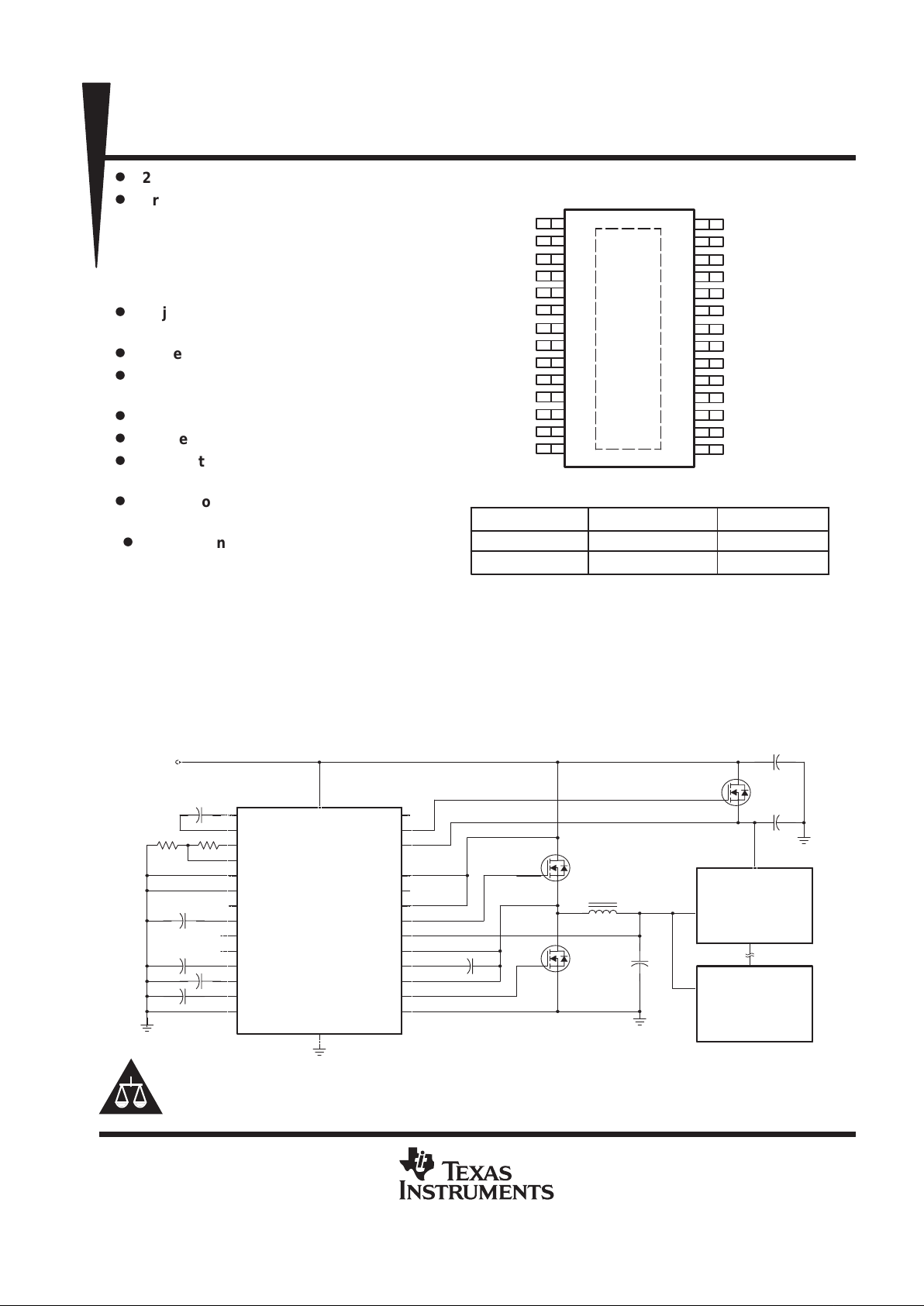
2.8 V – 5.5 V Input Voltage Range
D
Programmable Dual Output Controller
Supports Popular DSP, FPGA and
Microcontroller Core and I/O Voltages
– Switching Regulator Controls I/O Voltage
– Low Dropout Controller Regulates Core
Voltage
D
Adjustable Slow-Start for Simultaneous
Powerup of Both Outputs
D
Power Good Output Monitors Both Outputs
D
Fast Ripple Regulator Reduces Bulk
Capacitance for Lower System Costs
D
±1.5% Reference V oltage Tolerance
D
Efficiencies Greater Than 90%
D
Overvoltage, Undervoltage, and Adjustable
Overcurrent Protection
D
Drives Logic Level N-Channel MOSFETs
Through Entire Input Voltage Range
D
Evaluation Module TPS56302EVM–163
Available
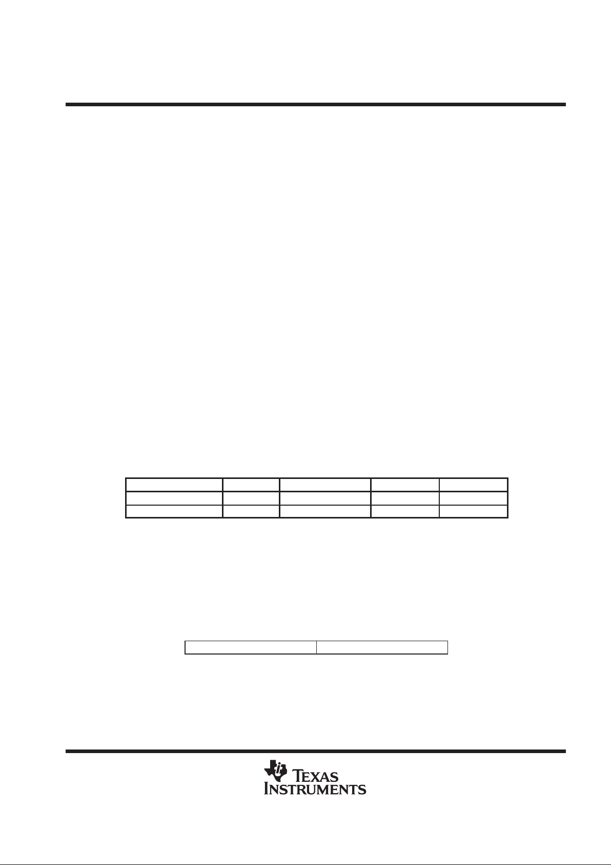
description
The high-performance TPS56302 synchronous-buck regulator provides two supply voltages to power the core
and I/O of digital signal processors. The TPS56302 is identical to the TPS56300 except that the reference
voltages of the LDO and switching regulator have been reversed. The switching regulator, using hysteretic
control with droop compensation, supports high current and efficiency for the I/O and other peripheral
components. The LDO controller, suitable for powering the core voltage, drives an external N-channel power
MOSFET and functions as an LDO regulator and as a power distribution switch.
typical design
+
+ +
U1
TPS56302PWP
CPC1
CPC2
VREFB
VHYST
DROOP
OCP
IOUT
SLOWST
VID0
VID1
BIAS
VLDODRV
VDRV
ANAGND
PwrPad
V
CC
DSP
V
CORE
V
I/O
Data
Data Bus
PERIPHERAL
V
I
(2.8 V – 5.5 V)
PWRGD
NGATE–LDO
VSEN–LDO
INHIBIT
IOUTLO
HISENSE
HIGHDR
VSEN–RR
LOSENSE/LOHIB
BOOT
BOOTLO
LOWDR
DRVGND
See Table 1
See Table 1
+
+
Copyright 2000, Texas Instruments Incorporated
PRODUCTION DATA information is current as of publication date.
Products conform to specifications per the terms of Texas Instruments
standard warranty. Production processing does not necessarily include
testing of all parameters.
Please be aware that an important notice concerning availability, standard warranty, and use in critical applications of
Texas Instruments semiconductor products and disclaimers thereto appears at the end of this data sheet.
PowerPAD is a trademark of Texas Instruments.
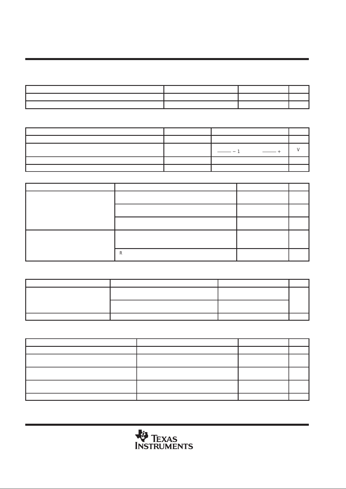
1
2
3
4
5
6
7
8
9
10
11
12
13
14
28
27
26
25
24
23
22
21
20
19
18
17
16
15
VID0
VID1
SLOWST
VHYST
VREFB
VSEN–RR
ANAGND
BIAS
VLDODRV
CPC1
V
CC
CPC2
VDRV
DRVGND
DROOP
OCP
IOUT
PWRGD
VSEN–LDO
NGATE–LDO
INHIBIT
IOUTLO
HISENSE
LOSENSE/LOHIB
HIGHDR
BOOT
BOOTLO
LDWDR
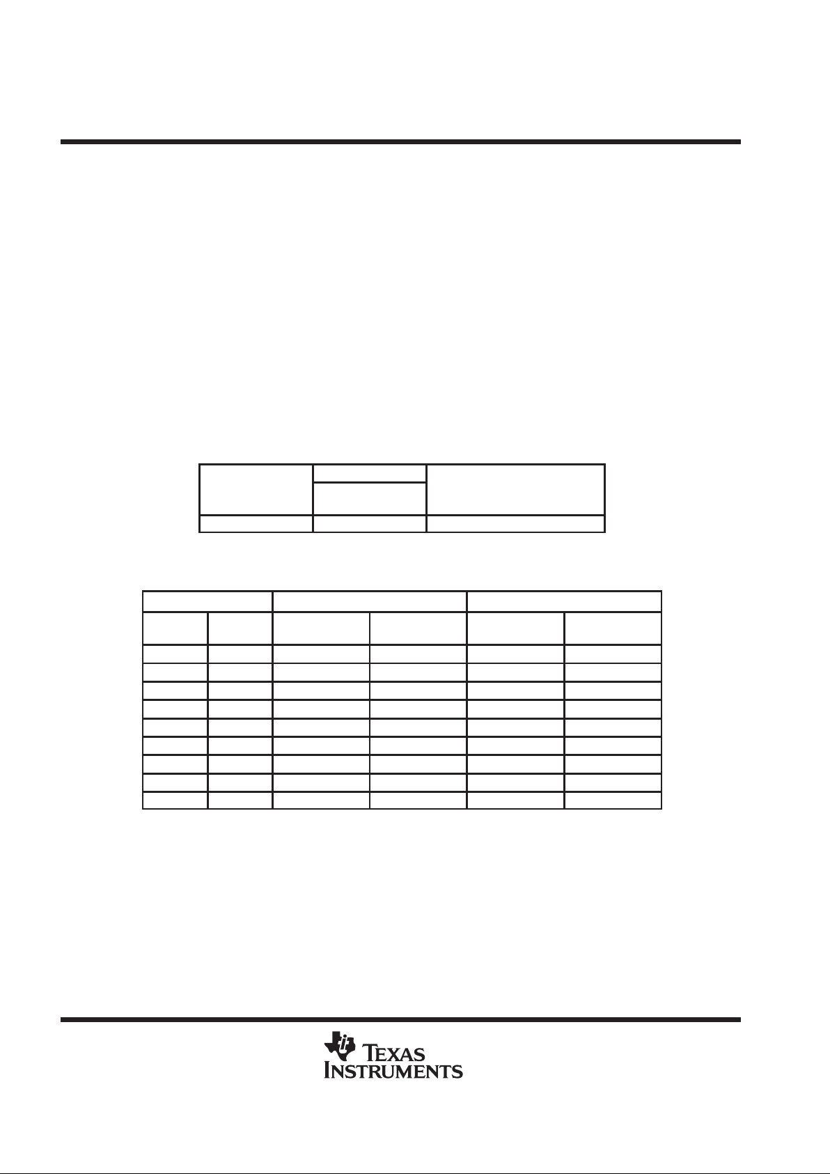
PWP PowerPAD PACKAGE
(TOP VIEW)
Thermal
Pad
OUTPUTS
V
OUT
–LDO
V
OUT
–Switcher
TPS56302
1.3 V TO 2.5 V
1.3 V TO 3.3 V
TPS56300
1.3 V TO 3.3 V
1.3 V TO 2.5 V
AVAILABLE VID CODE RANGES
NOTE: See Table 1 for actual VID codes.
TPS56302
DUAL-OUTPUT LOW-INPUT-VOLTAGE
DSP POWER SUPPLY CONTROLLER WITH SEQUENCING
SLVS289 – MARCH 2000
2
POST OFFICE BOX 655303 • DALLAS, TEXAS 75265
description (continued)
T o promote better system reliability during power up, voltage sequencing and protection are controlled such that
the core and I/O power up together with the same slow-start voltage. At power down, the LDO and ripple
regulator are discharged towards ground for added protection. The TPS56302 also includes inhibit, slow-start,
and under-voltage lockout features to aide in controlling power sequencing. A tri-level voltage identification
definition (VID) sets both regulated voltages to any of 9 preset voltage pairs from 1.3 V to 3.3 V . Other voltages
are possible by implementing an external voltage divider. Strong MOSFET drivers, with a typical peak current
rating of 2-A sink and source are included on chip, which allows paralleling MOSFET s to be driven and allowing
higher current to be controlled. The high-side driver features a floating bootstrap driver with an internal bootstrap
synchronous rectifier. Many protection features are incorporated within the device to ensure better system
integrity . An open-drain output power good status circuit monitors both output voltages, and is pulled low if either
output falls below the threshold. An over current shutdown circuit protects the high-side power MOSFET against
short-to-ground faults, while over voltage protection turns off the output drivers and LDO controller if either
output exceeds its threshold. Under voltage protection turns off the high-side and low-side MOSFET drivers and
the LDO controller if either output is 25% below V
REF
. Lossless current-sensing is implemented by detecting
the drain-source voltage drop across the high-side power MOSFET while it is conducting. The TPS56302 is fully
compliant with TI DSP power requirements.
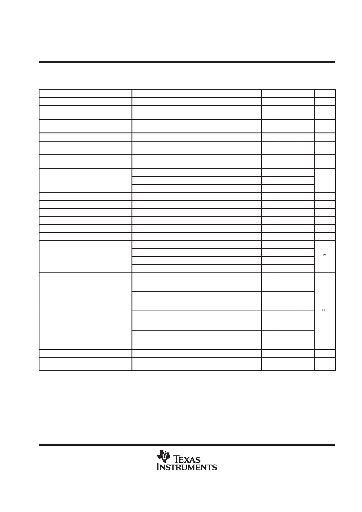
AVAILABLE OPTIONS
PACKAGES
T
J
TSSOP
†
(PWP)
EVALUATION MODULE
–40°C to 125°C TPS56302PWP TPS56302EVM–163 (SLVP163)
†
The PWP package is also available taped and reel. To order, add an R to the end of
the part number (e.g., TPS56302PWPR).
Table 1. Voltage Identification Code
¶#
VID TERMINALS
‡
56302 56300
VID1 VID0
V
REF–LDO
#
(VDC)
V
REF–RR
#
(VDC)
V
REF–RR
#
(VDC)
V
REF–LDO
#
(VDC)
0 0 1.30 1.50 1.30 1.50
0 1 1.50 1.80 1.50 1.80
0 2 1.30 1.80 1.30 1.80
1 0 1.80 3.30 1.80 3.30
1 1 1.30 1.30 1.30 1.30
1 2 2.50 3.30 2.50 3.30
2 0 1.30 2.50 1.30 2.50
2 1 1.50 3.30 1.50 3.30
2 2 1.80 2.50 1.80 2.50
‡
0 = ground (GND), 1 = floating(V
BIAS
/2), 2 = (V
BIAS
)
§
RR = Ripple Regulator, LDO = Low Drop-Out Regulator
¶
V
BIAS
/2 is internal, leave the VID pin floating. Adding an external 0.1-µF capacitor to ANAGND may be used
to avoid erroneous level.
#
External resistors may be used as a voltage divider (from V
OUT
to VSEN–xx to ground) to program output
voltages to other values.
TPS56302
DUAL-OUTPUT LOW-INPUT-VOLTAGE
DSP POWER SUPPLY CONTROLLER WITH SEQUENCING
SLVS289 – MARCH 2000
3
POST OFFICE BOX 655303 • DALLAS, TEXAS 75265
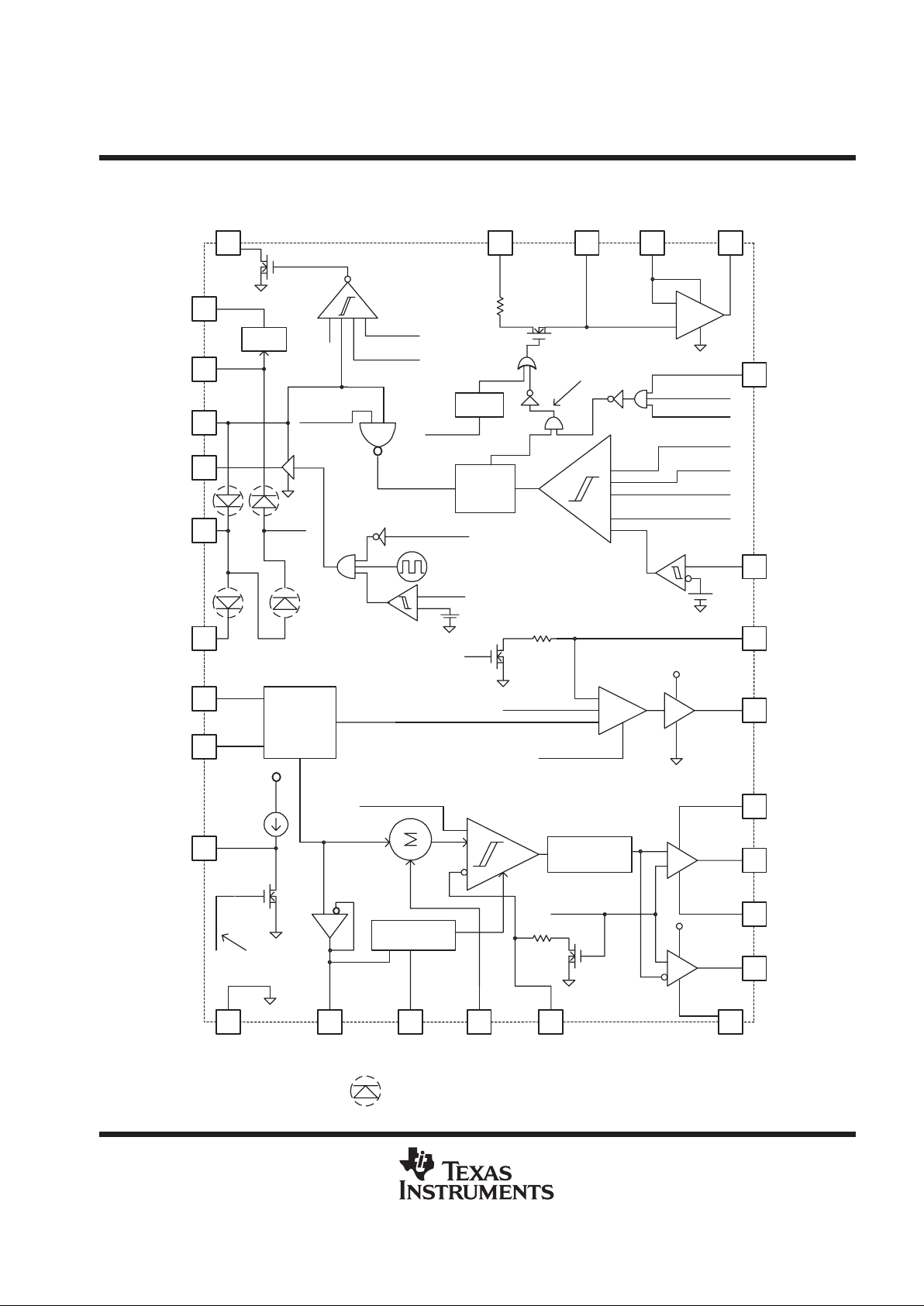
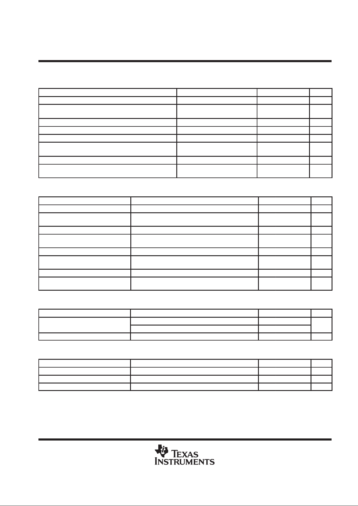
functional block diagram
CC
23
24
VLDODRV
NGATE–LDO
VSEN–LDO
RR_OVP
LDO_OVP
RR_UVP *
LDO_UVP *
SHUTDOWN
VID
2
1
VID0
VID1
VREF_LDO
VREF_RR
5
VREFB
Hysteresis
Setting
+
–
28
VHYST
6
VSEN–RR
Hysteresis
Comparator
Adaptive
Deadtime
15
18
16
14
17
VDRV
BOOT
HIGHDR
BOOTLO
LOWDR
DRVGND
22
11
INHIBIT
V
VDRV UVLO
V
3
SLOWST
SHUTDOWN
+
–
–
+
Delay
26202119
LOSENSE/
LOHIB
IOUTLO HISENSE
IOUT
HIGHDR
Ivrefb/5
Vbias
8
Bias
7
Reg.
VLDODRV
25
>0.93xVSEN–RR
>0.93xVSEN–LDO
4
DROOP
PWRGD
ANAGND
SHUTDOWN
27
125 mV
OCP
RS
Q
Fault
Latch
SHUTDOWN
INHIBIT
SLOWST
SLOWST
SHUTDOWN
SHUTDOWN
5 V
10
CPC1
9
12
CPC2
13
VDRV
VDRV
BOOT
–
+
E/A
Synchronous
FET
RR–Ripple Regulator
(see Table 1)
VDRV
* UVP is disabled during slowstart
CC
UVLO
TPS56302
DUAL-OUTPUT LOW-INPUT-VOLTAGE
DSP POWER SUPPLY CONTROLLER WITH SEQUENCING
SLVS289 – MARCH 2000
4
POST OFFICE BOX 655303 • DALLAS, TEXAS 75265
Terminal Functions
TERMINAL
NAME
NO.
DESCRIPTION
VID0 1 Voltage Identification input 0. The VID pins are tri-level programming pins that set the output voltages for both
converters. The code pattern for setting the output voltage is located in table 1. The VID pins are internally pulled to
V
BIAS
/2, allowing floating voltage set to logic 1 (see Table 1).
VID1 2 Voltage Identification input 1 (see VID0 pin description and Table 1).
SLOWST 3 Slow-start (soft start). A capacitor from pin 3 to GND sets the slow-start time for V
OUT-RR
and V
OUT-LDO
. Both supplies
will ramp-up together while tracking the slow-start voltage.
VHYST 4 Hysteresis set pin. The hysteresis equals 2 × (VREFB – VHYST).
VREFB 5 Buffered ripple regulator reference voltage from VID network.
VSEN-RR 6 Ripple regulator voltage sense input. This pin is connected to the ripple regulator output. It is used to sense the ripple
regulator voltage for regulation, OVP , UVP , and power good functions.. It is recommended that an RC low pass filter be
connected at this pin to filter high frequency noise.
ANAGND 7 Analog ground
BIAS 8 Analog BIAS pin. Recommended that a 1-µF capacitor be connected to ANAGND.
VLDODRV 9 Output of charge pump generated through bootstrap diode. Approximately equal to VDRV + VIN – 300 mV . Used as
supply for LDO driver and bias regulator. Recommended that a 1-µF capacitor be connected to DR VGND.
CPC1 10 Connect one end of charge pump capacitor. Recommended that a 1-µF capacitor be connected from CPC1 to CPC2.
V
CC
11 3.3 V or 5 V supply (2.8 V – 5.5 V). It is recommended that a low ESR capacitor be connected directly from VCC to
DRVGND (bulk capacitors supplied at power stage input).
CPC2 12 Other end of charge pump capacitor from CPC1.
VDRV 13 Regulated output of internal charge pump. Supplies DRIVE charge for the low-side MOSFET driver (5 V).
Recommended that a 10-µF capacitor be connected to DRVGND.
DRVGND 14 Drive ground. Ground for FET drivers. Connect to source of low-side FET.
LOWDR 15 Low drive. Output drive to synchronous rectifier low-side FET.
BOOTLO 16 Bootstrap low. This pin connects to the junction of the high-side and low-side FETs.
BOOT 17 Bootstrap pin. Connect a 1-µF low ESR capacitor to BOOTLO to generate floating drive for the high-side FET driver.
HIGHDR 18 High drive. Output drive to high-side power switching FETs
LOSENSE/
LOHIB
19 Low sense/low-side inhibit. This pin is connected to the junction of the high and low-side FET s and is used in current
sensing and the anti-cross-conduction to eliminate shoot-through current.
HISENSE 20 High current sense. For current sensing across high-side FETs, connect to the drain of the high-side FETs.
IOUTLO 21 Current sense low output. Voltage on this pin is the voltage on the LOSENSE pin when the high-side FETs are on.
INHIBIT 22 This pin inhibits the drive signals to the MOSFET drivers. The IC is in a low-current state if INHIBIT is grounded. It is
recommended that an external pullup resistor be connected to 5 V.
NGATE-LDO 23 Drives external N-channel power MOSFET to regulate LDO voltage to VREF-LDO.
VSEN–LDO 24 LDO voltage sense. This pin is connected to the LDO output. It is used to sense the LDO voltage for regulation, OVP,
UVP, and power good functions.
PWRGD 25 Power good. Power good signal goes high when output voltage is above 93% of V
REF
for both ripple regulator and
LDO. This is an open-drain output.
IOUT 26 Current signal output. Output voltage on this pin is proportional to the load current as measured across the high-side
FET s on-resistance. The voltage on this pin equals 2× RON×IOUT, where RON is the equivalent on-resistance of the
high-side FETs
OCP 27 Over current protection. Current limit trip point for ripple regulator is set with a resistor divider between the IOUT pin and
ANAGND. The trip point is typically 125 mV .
DROOP 28 Droop voltage. Voltage input used to set the amount of output voltage droop as a function of load current. The amount of
droop compensation is set with a resistor divider between the IOUT pin and ANAGND.
TPS56302
DUAL-OUTPUT LOW-INPUT-VOLTAGE
DSP POWER SUPPLY CONTROLLER WITH SEQUENCING
SLVS289 – MARCH 2000
5
POST OFFICE BOX 655303 • DALLAS, TEXAS 75265
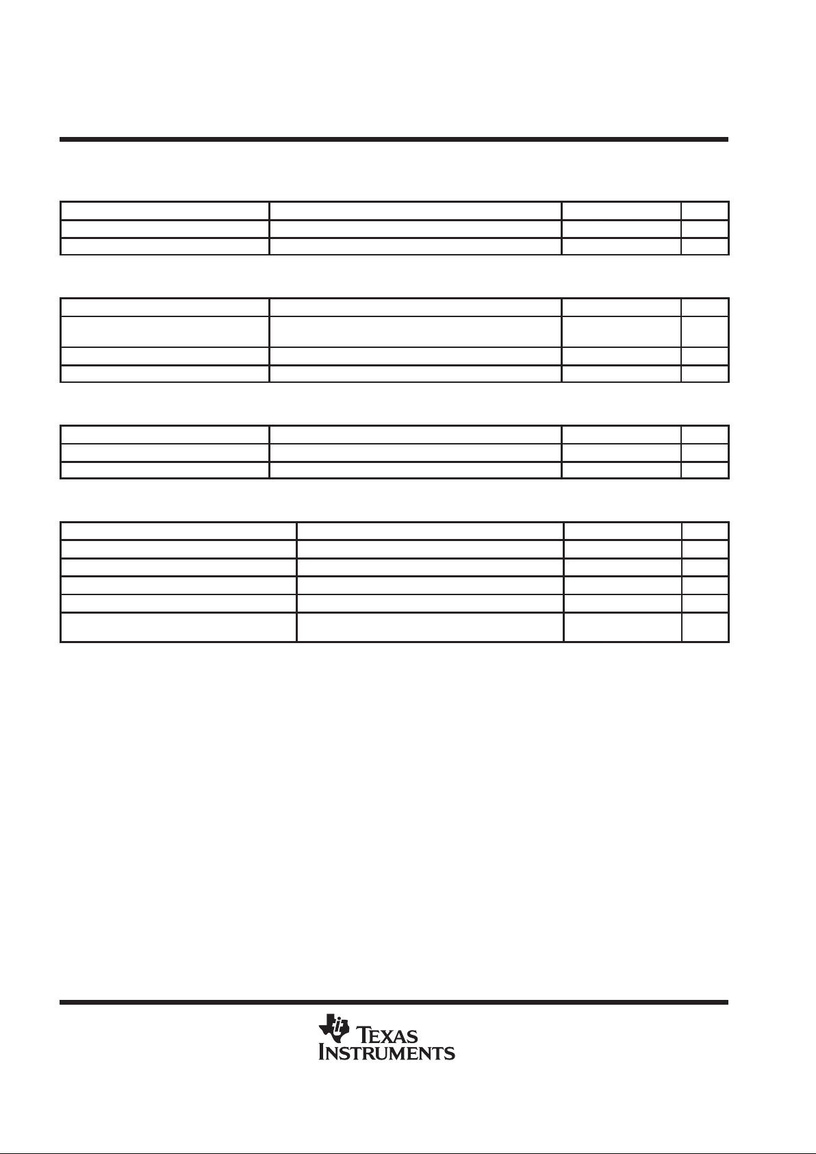
absolute maximum ratings over operating virtual junction temperature (unless otherwise noted)
†
Supply voltage range, V
CC
(see Note1) –0.3 V to 6 V. . . . . . . . . . . . . . . . . . . . . . . . . . . . . . . . . . . . . . . . . . . . . . .
Input voltage range: VDRV –0.3 V to 7 V. . . . . . . . . . . . . . . . . . . . . . . . . . . . . . . . . . . . . . . . . . . . . . . . . . . . . . . . .
BOOT to DRVGND (High-side Driver ON) –0.3 V to 15 V. . . . . . . . . . . . . . . . . . . . . . . . .
BOOT to BOOTLO –0.3 V to 7 V. . . . . . . . . . . . . . . . . . . . . . . . . . . . . . . . . . . . . . . . . . . . . .
BOOT to HIGHDRV –0.3 V to 7 V. . . . . . . . . . . . . . . . . . . . . . . . . . . . . . . . . . . . . . . . . . . . .
BOOTLO to DRVGND –0.5 V to 15 V. . . . . . . . . . . . . . . . . . . . . . . . . . . . . . . . . . . . . . . . . .
DRV to DRVGND –0.3 V to 7 V. . . . . . . . . . . . . . . . . . . . . . . . . . . . . . . . . . . . . . . . . . . . . . .
BIAS to ANAGND –0.3 V to 7 V. . . . . . . . . . . . . . . . . . . . . . . . . . . . . . . . . . . . . . . . . . . . . . .
INHIBIT –0.3 V to 7 V. . . . . . . . . . . . . . . . . . . . . . . . . . . . . . . . . . . . . . . . . . . . . . . . . . . . . . .
DROOP –0.3 V to V
CC
+ 0.3 V. . . . . . . . . . . . . . . . . . . . . . . . . . . . . . . . . . . . . . . . . . . . . . . .
OCP –0.3 V to 7 V. . . . . . . . . . . . . . . . . . . . . . . . . . . . . . . . . . . . . . . . . . . . . . . . . . . . . . . . . .
VID0, VID1 (tri-level terminals) –0.3 V to V
BIAS
+ 0.3 V. . . . . . . . . . . . . . . . . . . . . . . . . .
PWRGD –0.3 V to 6 V. . . . . . . . . . . . . . . . . . . . . . . . . . . . . . . . . . . . . . . . . . . . . . . . . . . . . . .
LOSENSE, LOHIB –0.5 V to 14 V. . . . . . . . . . . . . . . . . . . . . . . . . . . . . . . . . . . . . . . . . . . . .
IOUTLO –0.3 V to 14 V. . . . . . . . . . . . . . . . . . . . . . . . . . . . . . . . . . . . . . . . . . . . . . . . . . . . . .
HISENSE –0.3 V to 7 V. . . . . . . . . . . . . . . . . . . . . . . . . . . . . . . . . . . . . . . . . . . . . . . . . . . . . .
VSEN–LDO –0.3 V to 6 V. . . . . . . . . . . . . . . . . . . . . . . . . . . . . . . . . . . . . . . . . . . . . . . . . . . .
VSEN–RR –0.3 V to 6 V. . . . . . . . . . . . . . . . . . . . . . . . . . . . . . . . . . . . . . . . . . . . . . . . . . . . .
Voltage difference between ANAGND and DRVGND ±300 mV. . . . . . . . . . . . . . . . . . . . . . . . . . . . . . . . . . . . . . .
Continuous total power dissipation See Dissipation Rating Table. . . . . . . . . . . . . . . . . . . . . . . . . . . . . . . . . . . . .
Operating junction temperature range, T
J
–40°C to 125°C. . . . . . . . . . . . . . . . . . . . . . . . . . . . . . . . . . . . . . . . . . .
Storage temperature range, T
stg
–65°C to 150°C. . . . . . . . . . . . . . . . . . . . . . . . . . . . . . . . . . . . . . . . . . . . . . . . . . .
Lead temperature soldering 1,6 mm (1/16 inch) from case for 10 seconds 300°C. . . . . . . . . . . . . . . . . . . . . . .
†
Stresses beyond those listed under “absolute maximum ratings” may cause permanent damage to the device. These are stress ratings only, and
functional operation of the device at these or any other conditions beyond those indicated under “recommended operating conditions” is not
implied. Exposure to absolute-maximum-rated conditions for extended periods may affect device reliability.
NOTE 1: Unless otherwise specified, all voltages are with respect to ANAGND.
DISSIPATION RATING TABLE
PWP
TA < 25°C DERATING FACTOR
‡
TA = 70°C TA = 85°C
PowerPAD mounted 3.58 W 0.0358 W/°C 1.96 W 1.43 W
PowerPAD unmounted 1.78 W 0.0178 W/°C 0.98 W 0.71 W
‡
Test Board Conditions:
1.. Thickness: 0.062”
2. 3”× 3”
3. 2 oz. Copper traces located on the top of the board (0.071 mm thick )
4. Copper areas located on the top and bottom of the PCB for soldering
5. Power and ground planes, 1 oz. Copper (0.036 mm thick)
6. Thermal vias, 0.33 mm diameter, 1.5 mm pitch
7. Thermal isolation of power plane
For more information, refer to TI technical brief SLMA002.
JUNCTION-CASE THERMAL RESISTANCE TABLE
Junction-case thermal resistance
0.72 °C/W
TPS56302
DUAL-OUTPUT LOW-INPUT-VOLTAGE
DSP POWER SUPPLY CONTROLLER WITH SEQUENCING
SLVS289 – MARCH 2000
6
POST OFFICE BOX 655303 • DALLAS, TEXAS 75265
electrical characteristics TJ = 0° to 125°C, VCC = 2.8 V to 5.5 V (unless otherwise noted)
input
PARAMETER TEST CONDITIONS MIN TYP MAX UNITS
V
CC
Supply voltage range 2.8 5.5 V
I
CC
Quiescent current INHIBIT = 0 V, VCC = 5 V 15 mA
NOTE 2: Ensured by design, not production tested.
reference/voltage identification
PARAMETER TEST CONDITIONS MIN TYP MAX UNITS
VID0–VID1 High-level input voltage (2) V
BIAS
– 0.3 V V
VID0–VID1 Mid-level floating voltage (1)
V
BIAS
2
*
1
V
BIAS
2
)
1
V
VID0–VID1 Low-level input voltage (0) 0.3 V
Input pull-to-mid resistance 36.5 73 95 kΩ
cumulative reference
PARAMETER TEST CONDITIONS MIN TYP MAX UNITS
V
REF
= 1.3 V, Hysteresis window = 30 mV ,
TJ = 25°C
–1.3% 0.25% 1.3%
Cumulative accuracy ripple regulator
V
REF
= 1.3 V, Hysteresis window = 30 mV ,
TJ = –40°C, See Note 2
–0.2%
V
REF
= full range, Hysteresis window = 30 mV,
Droop = 0, See Note 2
–1.5% 1.5%
Cumulative accuracy LDO
V
REF
= 1.3 V, IO = 0.1 A,
Closed Loop, Pass device = IRFZ24N,
TJ = 25°C, See Note 2
–2% 2%
y
V
REF
= full range, IO = 0.1 A, Closed Loop,
Pass device = IRFZ24N, See Note 2
–2.5% 2.5%
NOTE 2. Ensured by design, not production tested.
buffered reference
PARAMETER CONDITIONS MIN TYP MAX UNITS
p
I
REFB
=50 µA, Accuracy from V
REF
nominal
V
REF
–1.5%
V
REF
V
REF
+1.5%
VREFB output voltage
I
REFB
=50 µA, Accuracy from V
REF
nominal
TJ = –40°C, See Note 2
V
REF
–0.6%
V
VREFB load regulation 10 µA < I
REFB
< 500 µA 2 mV
NOTE 2. Ensured by design, not production tested.
hysteretic comparator(ripreg)
PARAMETER TEST CONDITIONS MIN TYP MAX UNITS
Input bias current See Note 2 500 nA
Hysteresis accuracy
V
VREFB
– V
VHYST
= 15 mV,
Hysteresis window = 30 mV
–3.5 3.5 mV
Maximum hysteresis setting
V
VREFB
– V
VHYST
= 30 mV,
See Note 2
60 mV
Propagation delay time from VSENSE to HIGHDR or
LOWDR (excluding deadtime)
10 mV overdrive, 1.3 V <= V
REF
<= 3.3 V,
See Note 2
150 250 ns
Prefilter pole frequency See Note 2 5 MHz
NOTE 2. Ensured by design, not production tested.
TPS56302
DUAL-OUTPUT LOW-INPUT-VOLTAGE
DSP POWER SUPPLY CONTROLLER WITH SEQUENCING
SLVS289 – MARCH 2000
7
POST OFFICE BOX 655303 • DALLAS, TEXAS 75265
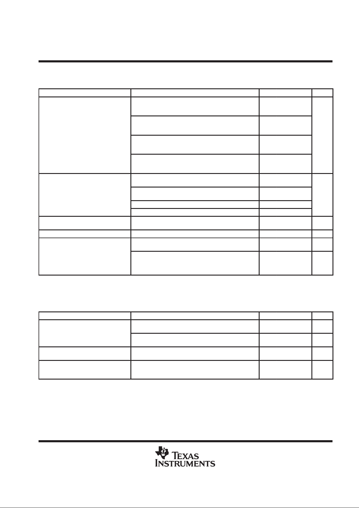
electrical characteristics TJ = 0° to 125°C, VCC = 2.8 V to 5.5 V (unless otherwise noted) (continued)
overvoltage protection
PARAMETER TEST CONDITIONS MIN TYP MAX UNITS
OVP ripple regulator trip point (RR) Upper threshold 112 115 120 %V
REF
Hysteresis (RR)
Upper threshold – lower threshold,
(see Note 2)
10 mV
Comparator propagation delay time (RR) V
overdrive
= 30 mV , See Note 2 1 µs
Deglitch time (includes comparator propagation delay time) (RR) V
overdrive
= 30 mV , See Note 2 2.25 11 µs
OVP LDO trip point (LDO) Upper threshold 112 115 120 % V
REF
Hysteresis (LDO)
Upper threshold – lower threshold,
(see Note 2)
10 mV
Comparator propagation delay time (LDO) V
overdrive
= 50 mV , See Note 2 1 µs
Deglitch time (includes comparator propagation delay time)
(LDO)
V
overdrive
= 50 mV , See Note 2 2.25 11 µs
NOTE 2. Ensured by design, not production tested.
undervoltage protection
PARAMETER CONDITIONS MIN TYP MAX UNITS
UVP ripple regulator trip point (RR) Lower threshold 70 75 80 % V
REF
Hysteresis (RR)
Upper threshold – lower threshold,
(see Note 2)
10 mV
Comparator propagation delay time (RR) V
overdrive
= 50 mV , See Note 2 1 µs
Deglitch time (includes comparator
propagation delay time) (RR)
V
overdrive
= 50 mV , See Note 2 0.1 1 ms
UVP LDO trip point (LDO) Lower threshold 70 75 80 % V
REF
Hysteresis (LDO)
Upper threshold – lower threshold,
(see Note 2)
10 mV
Comparator propagation delay time (LDO) V
overdrive
= 50 mV , See Note 2 1 µs
Deglitch time (includes comparator
propagation delay time) (LDO)
V
overdrive
= 50 mV , See Note 2 0.1 1 ms
NOTE 2. Ensured by design, not production tested.
inhibit comparator
PARAMETER CONDITIONS MIN TYP MAX UNITS
2.1 2.35
Start threshold
TJ = –40°C, See Note 2 2.1
V
Stop threshold 1.79 V
NOTE 2. Ensured by design, not production tested.
VDRV UVLO
PARAMETER CONDITIONS MIN TYP MAX UNITS
Start threshold See Note 2 4.9 V
Hysteresis See Note 2 0.3 0.35 V
Stop threshold See Note 2 4.4 V
NOTE 2. Ensured by design, not production tested.
TPS56302
DUAL-OUTPUT LOW-INPUT-VOLTAGE
DSP POWER SUPPLY CONTROLLER WITH SEQUENCING
SLVS289 – MARCH 2000
8
POST OFFICE BOX 655303 • DALLAS, TEXAS 75265
electrical characteristics TJ = 0° to 125°C, VCC = 2.8 V to 5.5 V (unless otherwise noted) (continued)
slow-start
PARAMETER CONDITIONS MIN TYP MAX UNITS
Charge current
V
(S/S)
= 0.5 V,
Resistance from VREFB pin to ANAGND = 20 kΩ
VREFB = 1.3 V, Ichg = (I
VREFB
/5)
10.4 13 15.6 µA
Discharge current V
(S/S)
= 1.3 V 3 mA
Comparator input offset voltage 10 mV
Comparator input bias current See Note 2 10 100 nA
Hysteresis accuracy –7.5 7.5 mV
Comparator propagation delay Overdrive = 10 mV, See Note 2 560 1000 ns
NOTE 2. Ensured by design, not production tested.
VCC UVLO
PARAMETER CONDITIONS MIN TYP MAX UNITS
(see Note 2) 2.72 2.80
Start threshold
TJ = –40°C, See Note 2 2.71
V
Stop threshold (see Note 2) 2.48 V
NOTE 2. Ensured by design, not production tested.
power good
PARAMETER CONDITIONS MIN TYP MAX UNITS
Undervoltage trip point ripple regulator
VIN and VDRV above UVLO thresholds 90 93 95
gg
(VSENSE–RR)
TJ = –40°C, See Note 2 93
% V
REF
Undervoltage trip point LDO
VIN and VDRV above UVLO thresholds 90 93 95
g
(VSENSE–LDO)
TJ = –40°C, See Note 2 93
% V
REF
Output saturation voltage IO=5 mA 0.5 0.75 V
Leakage current V
PGD
= 4.5 V 1 µA
V
REF
= 1.3 V, 1.5 V, or 1.8 V 50 75 mV
Hysteresis
V
REF
= 2.5 V, or 3.3 V 100 125 mV
Comparator high–low transition time
(propagation delay only)
See Note 2 1 µs
Comparator low–high transition time
(propagation delay + deglitch)
See Note 2 0.2 1 2 ms
NOTE 2. Ensured by design, not production tested.
droop compensation
PARAMETER CONDITIONS MIN TYP MAX UNITS
Initial accuracy V
DROOP
= 50 mV 46 54 mV
overcurrent protection (RR)
PARAMETER CONDITIONS MIN TYP MAX UNITS
OCP trip point 118 130 142 mV
Input bias current 300 nA
Comparator propagation delay time V
overdrive
= 30 mV , See Note 2 1 µs
Deglitch time (includes comparator
propagation delay time)
V
overdrive
= 30 mV , See Note 2 2.25 11 µs
NOTE 2. Ensured by design, not production tested.
TPS56302
DUAL-OUTPUT LOW-INPUT-VOLTAGE
DSP POWER SUPPLY CONTROLLER WITH SEQUENCING
SLVS289 – MARCH 2000
9
POST OFFICE BOX 655303 • DALLAS, TEXAS 75265
electrical characteristics TJ = 0° to 125°C, VCC = 2.8 V to 5.5 V (unless otherwise noted) (continued)
high-side VDS sensing
PARAMETER CONDITIONS MIN TYP MAX UNITS
Gain 2 V/V
Initial accuracy
V
HISENSE
= 3.3 V, V
IOUTLO
= 3.2 V,
Differential input to Vds sensing amp = 100 mV
194 208 mV
Common-mode rejection ratio
V
HISENSE
=2.8 V to 5.5 V ,
V
HISENSE
– V
IOUTLO
=100 mV
69 75 dB
Sink current (IOUTLO) 2.8 V < V
IOUTLO
< 5.5 V 250 nA
Source current (IOUT)
V
IOUT
= 0.5 V, V
HISENSE
=3.3 V ,
V
IOUTLO
=2.8 V
500 µA
Sink current (IOUT)
V
IOUT
= 0.05 V , V
HISENSE
=3.35 V ,
V
IOUTLO
=3.3 V
50 µA
V
HISENSE
=5.5 V , R
IOUT
= 10 kΩ 0 1.75
Output voltage swing
V
HISENSE
=4.5 V , R
IOUT
= 10 kΩ 0 1.5
V
V
HISENSE
=3 V, R
IOUT
= 10 kΩ 0 0.75
LOSENSE high-level input voltage V
HISENSE
=2.8 V , See Note 2 1.77 V
LOSENSE low-level input voltage V
HISENSE
=2.8 V , See Note 2 1.49 V
LOSENSE high-level input voltage V
HISENSE
=4.5 V , See Note 2 2.85 V
LOSENSE low-level input voltage V
HISENSE
=4.5 V , See Note 2 2.4 V
LOSENSE high-level input voltage V
HISENSE
=5.5 V , See Note 2 3.80 V
LOSENSE low-level input voltage V
HISENSE
=5.5 V , See Note 2 3.2 V
V
HISENSE =
6 V, See Note 2 70 90
p
V
HISENSE =
4.5 V , See Note 2 80 100
Sample/hold resistance
V
HISENSE =
3.6 V , See Note 2 90 120
Ω
V
HISENSE =
2.8 V , See Note 2 120 180
V
HISENSE
= 2.55 V ,
V
IOUTLO
pulsed from 2.55 V to 2.45 V ,
100 ns rise and fall times, See Note 2
4
Response time (measured from 90% of
V
HISENSE
= 2.8 V,
V
IOUTLO
pulsed from 2.8 V to 2.7 V ,
100 ns rise and fall times, See Note 2
3.5
(
V
IOUTLO
to 90% of V
IOUT
)
V
HISENSE
= 4.5 V,
V
IOUTLO
pulsed from 4.5 V to 4.4 V ,
100 ns rise and fall times, See Note 2
3
µ
s
V
HISENSE
= 5.5 V,
V
IOUTLO
pulsed from 5.5 V to 5.9 V ,
100 ns rise and fall times, See Note 2
3
Short circuit protection rising edge delay LOSENSE grounded, See Note 2 300 500 ns
Sample/hold switch turnon/turnoff delay
2.8 V < V
HISENSE
< 5.5 V,
V
LOSENSE
= V
HISENSE
, See Note 2
30 100 ns
NOTE 2. Ensured by design, not production tested.
TPS56302
DUAL-OUTPUT LOW-INPUT-VOLTAGE
DSP POWER SUPPLY CONTROLLER WITH SEQUENCING
SLVS289 – MARCH 2000
10
POST OFFICE BOX 655303 • DALLAS, TEXAS 75265
electrical characteristics TJ = 0° to 125°C, VCC = 2.8 V to 5.5 V (unless otherwise noted) (continued)
thermal shutdown
PARAMETER CONDITIONS MIN TYP MAX UNITS
Over temperature trip point See Note 2 145 °C
Hysteresis See Note 2 10 °C
NOTE 2. Ensured by design, not production tested.
synch charge pump regulator
PARAMETER CONDITIONS MIN TYP MAX UNITS
Internal oscillator frequency
2.8 V < VIN < 5.5 V, I
DRV
= 50 mA,
VDRV=5 V , See Note 2
200 300 400 kHz
Internal oscillator turnon threshold VCC above UVLO threshold, See Note 2 5.05 5.2 V
Internal oscillator turnon hysteresis VCC above UVLO threshold, See Note 2 20 mV
NOTE 2. Ensured by design, not production tested.
hysteretic comparator (charge pump)
PARAMETER CONDITIONS MIN TYP MAX UNITS
Threshold VIN above UVLO threshold, See Note 2 5.05 5.2 V
Hysteresis VIN above UVLO threshold, See Note 2 20 mV
NOTE 2. Ensured by design, not production tested.
deadtime circuit
PARAMETER CONDITIONS MIN TYP MAX UNITS
LOSENSE/LOHIB high level input voltage V
HISENSE
=2.55 V – 5.5 V , See Note 2 2.4 V
LOSENSE/LOHIB low level input voltage V
HISENSE
=2.55 V – 5.5 V , See Note 2 1.33 V
LOWDR high level input voltage V
HISENSE
=2.55 V–5.5 V , See Note 2 3 V
LOWDR low level input voltage V
HISENSE
=2.55 V–5.5 V , See Note 2 1.7 V
Driver nonoverlap time
C
LOWDR
= 9 nF, 10% threshold on LOWDR,
VDRV=5 V
40 170 ns
NOTE 2. Ensured by design, not production tested.
TPS56302
DUAL-OUTPUT LOW-INPUT-VOLTAGE
DSP POWER SUPPLY CONTROLLER WITH SEQUENCING
SLVS289 – MARCH 2000
11
POST OFFICE BOX 655303 • DALLAS, TEXAS 75265
electrical characteristics TJ = 0° to 125°C, VCC = 2.8 V to 5.5 V (unless otherwise noted) (continued)
output drivers (see Note 5)
PARAMETER CONDITIONS MIN TYP MAX UNITS
Duty cycle < 2%, tpw < 100 us,
V
BOOT
– V
BOOTLO
= 4.5 V,
V
HIGHDR
= 4 V (sink), See Note 2 and Figure 15
0.7 2
p
Duty cycle < 2%, tpw < 100 us,
V
BOOT
– V
BOOTLO
= 4.5 V,
V
HIGHDR
= 0.5 V (source), See Note 2 and Figure 15
1.2 2
Peak output current
Duty cycle < 2%, tpw < 100 µs,
V
DRV
= 4.5 V, V
LOWDR
= 4 V (sink),
See Note 2 and Figure 15
1.3 2
A
Duty cycle < 2%, tpw < 100 us,
V
DRV
= 4.5 V, V
LOWDR
= 0.5 V (source),
See Note 2 and Figure 15
1.4 2
V
BOOT
– V
BOOTLO
= 4.5 V, V
HIGHDR
= 0.5 V,
See Note 2
5
Output resistance
V
BOOT
– V
BOOTLO
= 4.5 V, V
HIGHDR
= 4 V,
See Note 2
45
Ω
V
DRV
= 4.5 V, V
LOWDR
= 0.5 V , See Note 2 9
V
DRV
= 4.5 V, V
LOWDR
= 4 V, See Note 2 45
HIGHDR rise/fall time
CL = 3.3 nF, V
BOOT
= 4.5 V ,
V
BOOTLO
=grounded, See Note 2
60 ns
LOWDR rise/fall time CL = 3.3 nF, V
DRV
= 4.5 V , See Note 2 40 ns
INHIBIT grounded, VIN < UVLO, V
BOOT
=6 V ,
BOOTLO grounded
10 µA
High-side driver quiescent current
INHIBIT connected to +5 V , VIN > UVLO
f
(swx)
= 200 kHz, V
BOOT
= 5.5 V,
BOOTLO = 0, C
HIGHDR
= 50 pF,
See Note 2
2 mA
NOTES: 2. Ensured by design, not production tested.
5. The pullup/pulldown circuits of the drivers are bipolar and MOSFET transistors in parallel. The peak output current rating is the
combined current from the bipolar and MOSFET transistors. The output resistance is the R
ds(on)
of the MOSFET transistor when
the voltage on the driver output is less than the saturation voltage of the bipolar transistor.
LDO N-channel output driver
PARAMETER CONDITIONS MIN TYP MAX UNITS
p
V
LDODRV
= 7.5 V, V
N–DRV
= 3 V (source),
V
IOSENSE
= 0.9 × V
LDOREF
, See Note 2
100 µA
Peak output current
V
LDODRV
= 7.5 V, V
N–DRV
=0 V (sink),
V
IOSENSE
= 1.1 × V
LDOREF
, See Note 2
1.5 mA
Open loop voltage gain
(V
NGATE–LDO
/ V
SENSE–LDO
)
7.5 V ≥ V
NGATE–LDO
≥ 0.5 V, VIN = 5.5 V,
See Note 2
3000
(70)
V/V
(dB)
Power supply ripple rejection
f = 1 kHz, CO=10 µF,
5.5 V ≥ VIN ≥ 2.55 V, TJ=125 °C,
See Note 2
60 dB
NOTE 2. Ensured by design, not production tested.

TPS56302
DUAL-OUTPUT LOW-INPUT-VOLTAGE
DSP POWER SUPPLY CONTROLLER WITH SEQUENCING
SLVS289 – MARCH 2000
12
POST OFFICE BOX 655303 • DALLAS, TEXAS 75265
electrical characteristics TJ = 0° to 125°C, VCC = 2.8 V to 5.5 V (unless otherwise noted) (continued)
V
SENSE–RR
and V
SENSE–LDO
discharge
PARAMETER CONDITIONS MIN TYP MAX UNITS
V
SENSE–RR
discharge FET current saturation V
SENSE–RR
= 1.5 V , See Note 2 5 mA
V
SENSE–RR
discharge series resistance (limits current) INHIBIT = 0 V, VIN = 5.5 V 1 kΩ
V
SENSE–RR
discharge FET propagation delay time See Note 2 100 ns
V
SENSE–LDO
discharge FET current saturation V
SENSE–LDO
= 3.3 V , See Note 2 5 mA
V
SENSE–LDO
discharge series resistance (limits current) INHIBIT = 0 V, VIN = 5.5 V, 1 kΩ
V
SENSE–LDO
discharge FET propagation delay time See Note 2 100 ns
NOTE 2. Ensured by design, not production tested.
detailed description
reference/voltage identification
The reference/voltage identification definition (VID) section consists of a temperature compensated bandgap
reference and a 2-pin voltage selection network. Both ripple regulator and LDO reference voltages are
programmed with each VID setting. The 2 VID pins are inputs to the VID selection network and are tri-level inputs
that may be set to GND, floating (V
BIAS
/2), or V
BIAS
. The VID codes allow the controller to power both current
and future DSP products. The output voltages may also be programmed by external resistor voltage dividers
for any values not included in the VID code settings. Refer to Table 1 for the VID code settings. The output
voltages of the VID network, V
REF–RR
, is within 1.5% and V
REF–LDO
is within 2.5% of the nominal setting over
the VID range of 1.3 V to 3.3 V. The reference tolerance conditions include a junction temperature range of
–40_C to +125_C and a VCC supply voltage range of 2.8 V to 5.5 V . The V
REF–RR
output of the reference/VID
network is indirectly brought out through a buffer to the VREFB pin. The voltage on this pin will be within 1.5%
of V
REF–RR
. It is not recommended to drive loads with VREFB, other than setting the hysteresis of the hysteretic
comparator, because the current drawn from VREFB sets the charging current for the slow-start capacitor . Refer
to the Slow-start section of this document for additional information.
hysteretic comparator
The hysteretic comparator regulates the output voltage of the synchronous-buck converter. The hysteresis is
set by 2 external resistors and is centered around V
REF
. The two external resistors form a resistor divider from
VREFB to ANAGND, and the divided down voltage connects to the VHYST pin. The hysteresis of the
comparator will be equal to twice the voltage difference that is across the VREFB and VHYST pins. The
propagation delay from the comparator inputs to the driver outputs is 250 ns maximum. The maximum
hysteresis setting is 60 mV.
low-side driver
The low-side driver is designed to drive low r
DS(on)
logic-level N-channel MOSFETs. The current rating of the
driver is 2-A typical, source and sink. The bias to the low-side driver is internally connected to the regulated
synchronous charge pump output.
high-side driver
The high-side driver is designed to drive low r
DS(on)
logic-level N-channel MOSFET s. The current rating of the
driver is 2 amps typical, source and sink. The high-side driver can be configured either as a floating bootstrap
driver or as a ground-reference driver. When configured as a floating driver, the bias voltage to the driver is
developed from the charge pump VDRV voltage. The internal synchronous bootstrap rectifier, connected
between the VDRV and BOOT pins, is a synchronously-rectified MOSFET for improved drive efficiency. The
maximum voltage that can be applied between the BOOT pin and ground is 14 V.

TPS56302
DUAL-OUTPUT LOW-INPUT-VOLTAGE
DSP POWER SUPPLY CONTROLLER WITH SEQUENCING
SLVS289 – MARCH 2000
13
POST OFFICE BOX 655303 • DALLAS, TEXAS 75265
detailed description (continued)
deadtime control
Deadtime control prevents shoot-through current from flowing through the main power FETs during switching
transitions by actively controlling the turnon time of the MOSFET drivers. The high-side driver is not allowed
to turn on until the gate drive voltage to the low-side FET is below 1 V, and the low-side driver is not allowed
to turn on until the voltage at the junction of the 2 FETs (Vphase) is below 2 V.
current sensing
Current sensing is achieved by sampling and holding the voltage across the high-side power FET while the
high-side FET is on. The sampling network consists of an internal 60-Ω switch and an external hold capacitor.
Internal logic controls the turnon and turnoff of the sample/hold switch such that the switch does not turn on until
the Vphase voltage transitions high, and the switch turns off when the input to the high-side driver goes low.
Thus sampling will occur only when the high-side FET is conducting current. The voltage on the IOUT pin equals
2 times the sensed high-side voltage.
droop compensation
The droop compensation network reduces the load transient overshoot / undershoot on V
OUT
, relative to V
REF
(see the
application information
section of this document for more details). V
OUT
is programmed to a voltage
greater than V
REF
by an external resistor divider from V
OUT
to the VSENSE pin to reduce the undershoot on
V
OUT
during a low to high load transient. The overshoot during a high to low load transient is reduced by
subtracting the voltage that is on the DROOP pin from V
REF
. The voltage on the IOUT pin is divided down with
an external resistor divider, and connected to the DROOP pin.
inhibit
INHIBIT is a TTL-compatible comparator pin that is used to enable the controller. When INHIBIT is lower than
the threshold, the output drivers are low and the slow-start capacitor is discharged. When INHIBIT goes high
(above 2.1 V), the short across the slow-start capacitor is released and normal converter operation begins.
When another system logic supply is connected to the INHIBIT pin, this pin controls power sequencing by
locking out controller operation until the system logic supply exceeds the input threshold voltage of the inhibit
circuit; thus the +3.3-V supply and another system logic supply (either +5 V or +12 V) must be above UVLO
thresholds before the controller is allowed to start up. T oggling the INHIBIT pin from low to high or recycling V
CC
clears the fault latch.
slow-start
The slow-start circuit controls the rate at which both V
OUT–RR
and V
OUT–LDO
power up (at the same time). A
capacitor is connected between the SLOWST and ANAGND pins and is charged by an internal current source.
The value of the current source is proportional to the reference voltage, so that the charging rate of C
SLOWST
is proportional to the ripple regulator reference voltage. The slow-start charging current is determined by the
following equation:
I
SLOWSTART
+
I
VREFB
5
Where I
VREFB
is the current flowing out of the VREFB pin. It is recommended that no additional loads be
connected to VREFB, other than the resistor divider for setting the hysteresis voltage. Thus these resistor values
will determine the slow-start charging current. The maximum current that can be sourced by the VREFB circuit
is 500 µA. The equation for the slow-start time is:
T
SLOWSTART
+5
C
SLOWSTART
R
VREFB
Where R
VREFB
is the total external resistance from VREFB to ANAGND.

TPS56302
DUAL-OUTPUT LOW-INPUT-VOLTAGE
DSP POWER SUPPLY CONTROLLER WITH SEQUENCING
SLVS289 – MARCH 2000
14
POST OFFICE BOX 655303 • DALLAS, TEXAS 75265
detailed description (continued)
VCC and VDRV undervoltage lockout
The VCC undervoltage lockout circuit disables the controller while the VCC supply is below the 2.8-V start
threshold. The VDRV undervoltage lockout circuit disables the controller while the VDRV supply is below the
4.9 V start threshold during powerup. While the controller is disabled, the output drivers will be low, the LDO
drive is off, and the slow-start capacitor will be shorted. When V
CC
and VDRV exceed the start threshold, the
short across the slow-start capacitor is released and normal converter operation begins. Recycling VCC or
toggling the INHIBIT pin from low to high clears the fault latch.
power good
The power good circuit monitors for an undervoltage condition on V
OUT–RR
and V
OUT–LDO
. The power good
(PWRGD) pin is pulled low if either V
OUT–RR
is 7% below V
REF–RR
, or V
OUT–LDO
is 7% below V
REF–LDO
.
PWRGD is an open drain output. The PWRGD pin is also pulled down, if either V
CC
or VDRV are below their
UVLO thresholds.
overvoltage protection
The overvoltage protection circuit monitors V
OUT–RR
and V
OUT–LDO
for an overvoltage condition. If V
OUT–RR
or V
OUT–LDO
are 15% above their reference voltage, then a fault latch is set and both output drivers and LDO
are turned off. The latch remains set until the V
CC
or inhibit voltages go below their undervoltage lockout turnoff
values. A 1-µs to 5 µs deglitch timer is included for noise immunity.
overcurrent protection
The overcurrent protection circuit monitors the current through the high-side FET. The overcurrent threshold
is adjustable with an external resistor divider between IOUT and ANAGND pins, with the divider voltage
connected to the OCP pin. If the voltage on the OCP pin exceeds 125 mV , a fault latch is then set and the output
drivers are turned off. The latch remains set until the VCC or inhibit voltages go below their undervoltage lockout
values. A 1-µs to 5-µs deglitch timer is included for noise immunity . The OCP circuit is also designed to protect
the high-side power FET against a short-to-ground fault on the terminal common to both power FETs.
undervoltage protection
The undervoltage protection circuit monitors V
OUT–RR
and V
OUT–LDO
for an undervoltage condition. If V
OUT–RR
or V
OUT–LDO
is 15% below their reference voltage, then a fault latch is set and both output drivers and LDO are
turned off. The latch remains set until the VCC or inhibit voltages go below their undervoltage lockout values.
A 100-µs to 1-ms deglitch timer is included for noise immunity.
synchronous charge pump
The regulated synchronous charge pump provides drive voltage to the low-side driver at VDRV (5 V), and to
the high-side driver configured as a floating driver. The minimum drive voltage is 4.5 V, (typical is 5 V). The
minimum short-circuit current is 80 mA. The bootstrap capacitor is used to provide voltage for the high-side FET ,
the power for VLDODRV, and the bias regulator . Instead of diodes, synchronous rectified MOSFETs are used
to reduce voltage drop losses and allow a lower input voltage threshold. The charge pump oscillator operates
at 300 kHz until the UVLO VDRV is set; after which it is synchronized to the converter switching frequency and
is turned on and off to regulate VDRV at 5 V.
The charge pump is designed to operate at a switching frequency of 200 kHz to 400 kHz. Operation at low
frequency may require larger capacitors on the CPCx and VDRV pins. Higher frequencies (> 400 kHz) may not
be possible.
power sequence
The V
OUT–LDO
voltage is powered up with respect to the same slow-start reference voltage as the V
OUT–RR
Also, at power down, the V
OUT–RR
and V
OUT–LDO
are discharged to ground through P-channel MOSFET s in
series with 1-kΩ resistors.

TPS56302
DUAL-OUTPUT LOW-INPUT-VOLTAGE
DSP POWER SUPPLY CONTROLLER WITH SEQUENCING
SLVS289 – MARCH 2000
15
POST OFFICE BOX 655303 • DALLAS, TEXAS 75265
TYPICAL CHARACTERISTICS
Figure 1
10
11
12
13
0 25 50 75 100 125
Quiescent Current – mA
QUIESCENT CURRENT
vs
JUNCTION TEMPERATURE
TJ – Junction Temperature – °C
VCC = 3.3 V
INHIBIT = 0 V
Figure 2
150
155
160
165
170
175
180
0 25 50 75 100 125
VCC UVLO HYSTERESIS
vs
JUNCTION TEMPERATURE
TJ – Junction Temperature – °C
UVLO Hysteresis – mVV
CC
Figure 3
2.65
2.675
2.700
2.725
2.750
0 25 50 75 100 125
VCC UVLO START THRESHOLD VOLTAGE
vs
JUNCTION TEMPERATURE
TJ – Junction Temperature – °C
UVLO Start Threshold Voltage – VV
CC
Figure 4
TJ – Junction Temperature – °C
SLOW-START CHARGE CURRENT
vs
JUNCTION TEMPERATURE
12
10
25 75
14
13
11
50 100 125
15
0
Slowstart Charge Current – Aµ

TPS56302
DUAL-OUTPUT LOW-INPUT-VOLTAGE
DSP POWER SUPPLY CONTROLLER WITH SEQUENCING
SLVS289 – MARCH 2000
16
POST OFFICE BOX 655303 • DALLAS, TEXAS 75265
TYPICAL CHARACTERISTICS
Figure 5
SLOW-START TIME
vs
SUPPLY CURRENT (VREFB)
110
ICC – Supply Current (VREFB) – µA
1000
1
10
Slowstart Time – ms
VCC = 3.3 V
V
(VREFB)
= 1.3 V
CS = 0.1 µF
TJ = 27°C
100 1000
100
Figure 6
SLOW-START TIME
†
vs
SLOW-START CAPACITANCE
0.0001 0.0010
Slow-start Capacitance – µF
100
10
1
0.1
Slowstart Time – ms
VCC = 3.3 V
V
(VREFB)
= 1.3 V
I
(VREFB)
= 65 µA
TJ = 25°C
0.0100 0.1000 1
Figure 7
DRIVER
RISE TIME
vs
GATE CAPACITANCE
0.1 1
Gate Capacitance – nF
100
1
10
– Rise Time – ns
10 100
t
r
1000
TJ = 27°C
High Side
Low Side
Figure 8
Gate Capacitance – nF
0.1 1
1000
1
10
10 100
100
– Fall Time – nst
f
DRIVER
FALL TIME
vs
GATE CAPACITANCE
TJ = 27°C
High Side
Low Side

TPS56302
DUAL-OUTPUT LOW-INPUT-VOLTAGE
DSP POWER SUPPLY CONTROLLER WITH SEQUENCING
SLVS289 – MARCH 2000
17
POST OFFICE BOX 655303 • DALLAS, TEXAS 75265
TYPICAL CHARACTERISTICS
Figure 9
1.0
1.5
2.0
2.5
3.0
3.5
4.0
4.5
5.0
0 25 50 75 100 125
DRIVER
HIGH-SIDE OUTPUT RESISTANCE
vs
JUNCTION TEMPERATURE
TJ – Junction Temperature – °C
– High-Side Output Resistance –R
O
Ω
Figure 10
0
1
2
3
4
5
6
7
8
0 25 50 75 100 125
DRIVER
LOW-SIDE OUTPUT RESISTANCE
vs
JUNCTION TEMPERATURE
TJ – Junction Temperature – °C
– Low-Side Output Resistance –R
O
Ω
Figure 11
Input Current – A
DRIVER
CURRENT
vs
OUTPUT VOLTAGE
VO – Output Voltage – V
1
0
13
2
1.5
0.5
245
2.5
0
3
7689
4
3.5
4.5
5
2 A Typical
4.5 V
Figure 12
4.65
4.66
4.67
4.68
4.69
4.70
0 25 50 75 100 125
VDRV UVLO Start Threshold V oltage – V
VDRV UVLO START THRESHOLD VOLTAGE
vs
JUNCTION TEMPERATURE
TJ – Junction Temperature – °C

TPS56302
DUAL-OUTPUT LOW-INPUT-VOLTAGE
DSP POWER SUPPLY CONTROLLER WITH SEQUENCING
SLVS289 – MARCH 2000
18
POST OFFICE BOX 655303 • DALLAS, TEXAS 75265
TYPICAL CHARACTERISTICS
Figure 13
100
120
140
160
180
200
220
240
260
280
300
0 25 50 75 100 125
VDRV UVLO Hysteresis – mV
VDRV UVLO HYSTERESIS
vs
JUNCTION TEMPERATURE
TJ – Junction Temperature – °C
Figure 14
88
89
90
91
92
93
94
95
96
0 25 50 75 100 12
5
Ripple Regulator Powergood Threshold – %
RIPPLE REGULATOR
POWER GOOD THRESHOLD
vs
JUNCTION TEMPERATURE
TJ – Junction Temperature – °C
Figure 15
2.000
2.025
2.050
2.075
2.100
0 25 50 75 100 125
INHIBIT Start Threshold Voltage – V
INHIBIT START THRESHOLD VOLTAGE
vs
JUNCTION TEMPERATURE
TJ – Junction Temperature – °C
Figure 16
90
100
110
120
130
140
0 25 50 75 100 125
INHIBIT Hysteresis Voltage – mV
INHIBIT HYSTERESIS VOLTAGE
vs
JUNCTION TEMPERATURE
TJ – Junction Temperature – °C

TPS56302
DUAL-OUTPUT LOW-INPUT-VOLTAGE
DSP POWER SUPPLY CONTROLLER WITH SEQUENCING
SLVS289 – MARCH 2000
19
POST OFFICE BOX 655303 • DALLAS, TEXAS 75265
TYPICAL CHARACTERISTICS
Figure 17
TJ – Junction Temperature – °C
RIPPLE REGULATOR OVP THRESHOLD
vs
JUNCTION TEMPERATURE
114
112
25 75
116
115
113
50 100 125
117
0
Ripple Regulator OVP Threshold – %
118
Figure 18
TJ – Junction Temperature – °C
RIPPLE REGULATOR UVP THRESHOLD
vs
JUNCTION TEMPERATURE
73
71
25 75
75
74
72
50 100 125
76
0
Ripple Regulator UVP Threshold – %
77
TJ – Junction Temperature – °C
OCP THRESHOLD VOLTAGE
vs
JUNCTION TEMPERATURE
129
25 75
133
131
50 100 125
135
0
OCP Treshhold Voltage – mV
Figure 19

TPS56302
DUAL-OUTPUT LOW-INPUT-VOLTAGE
DSP POWER SUPPLY CONTROLLER WITH SEQUENCING
SLVS289 – MARCH 2000
20
POST OFFICE BOX 655303 • DALLAS, TEXAS 75265
TYPICAL CHARACTERISTICS
112
113
114
115
116
117
118
0 25 50 75 100 125
LDO OVP Threshold – %
LDO OVP THRESHOLD
vs
JUNCTION TEMPERATURE
TJ – Junction Temperature – °C
Figure 20
TJ – Junction Temperature – °C
LDO UVP THRESHOLD
vs
JUNCTION TEMPERATURE
73
71
25 75
75
74
72
50 100 125
76
0
LDO UVP Threshold – %
77
Figure 21

TPS56302
DUAL-OUTPUT LOW-INPUT-VOLTAGE
DSP POWER SUPPLY CONTROLLER WITH SEQUENCING
SLVS289 – MARCH 2000
21
POST OFFICE BOX 655303 • DALLAS, TEXAS 75265
APPLICATION INFORMATION
evaluation module
In many DSP applications, the voltage bus powering DSP I/O also has to power peripheral circuitry . The total
current is much higher than the requirement for the I/O only . This is the reason to use the high-efficiency ripple
regulator to power I/O. In turn, the core power is delivered by LDO output. Since the I/O voltage is lower than
the input voltage in cases such as 5-V input, but higher than the core voltage, the ripple regulator output should
be used as the input voltage for LDO to achieve higher efficiency . In EVM testing, J1–4 (RR–OUT) is connected
to J2–1(VI–LDO). The test results displayed in this section are all based on this configuration.
JP2
JP1
PwrPad
U1
TPS563xxPWP
JP3
TP8
TP7
E1
Q1:A
Q4
TP11
TP3
TP1
Q1:B
Q5
+
TP2
FB2
J2
+
+
TP6
TP5
FB1
+ + +
TP10
+
L1
3.3 uH
+ +
TP4
J1
Figure 22. EVM Schematic
Table 2. EVM Input and Outputs
V
IN
I
IN
V
RR
I
RR
V
LDO
I
LDO
5 V 4 A 3.3 V 4 A 1.8 V 0.5 A

TPS56302
DUAL-OUTPUT LOW-INPUT-VOLTAGE
DSP POWER SUPPLY CONTROLLER WITH SEQUENCING
SLVS289 – MARCH 2000
22
POST OFFICE BOX 655303 • DALLAS, TEXAS 75265
APPLICATION INFORMATION
Table 3. Ripple Regulator Power Stage Components
Ripple Regulator Section
Ref Des Function 4A (EVM Design) 8A
†
12A
†
20A
†
C3, C6 Input bulk
capacitor
C3: open
C6: 150 µF
(Sanyo,
6TPB150M)
C3: 150 µF
C6: 150 µF
(Sanyo,
6TPB150M)
C3: 150 µF
C6: 150 µF
(Sanyo,
6TPB150M)
C3: 150 µF
C6: 2x150 µF
(Sanyo,
6TPB150M)
C11, C2 Input high-freq
capacitor
C2: 0.1 µF
C11: 0.1 µF
(muRata
GRM39X7R104K016A,
0.1 µF, 16–V, X7R)
C2: 0.1 µF
C11: 0.1 µF
(muRata
GRM39X7R104K016A,
0.1 µF, 16–V, X7R)
C2: 0.1 µF
C11: 0.1 µF
(muRata
GRM39X7R104K016A, 0.1
µF, 16–V , X7R)
C2: 0.33 µF
C11: 0.33 µF
(muRata
GRM39X7R334K016A,
0.33 µF, 16–V, X7R)
C13, C14 Output bulk
capacitor
C13: 150 µF
(Sanyo, 6TPB150M)
C14: open
C13: 150 µF
(Sanyo, 6TPB150M)
C14: open
C13: 150 µF
C14: 150 µF
(Sanyo, 6TPB150M)
C13: 150 µF
C14: 150 µF
(Sanyo, 6TPB150M)
C15,C30,
C31
Output mid-freq
capacitor
C15: open
C30: 10 µF
C31: 10 µF
(muRata
GRM39X7R106K016A,
10 µF, 16–V, X7R)
C15: open
C30: 10 µF
C31: 10 µF
(muRata
GRM39X7R106K016A,
10 µF, 16–V, X7R)
C15: 10 µF
C30: 10 µF
C31: 10 µF
(muRata
GRM39X7R106K016A, 10
µF, 16–V , X7R)
C15: 10 µF
C30: 10 µF
C31: 10 µF
(muRata
GRM39X7R106K016A,
10 µF, 16–V, X7R)
C16 Output high-freq
capacitor
open 0.1 µF
(muRata
GRM39X7R104K016A,
0.1 µF, 16–V, X7R)
0.1 µF
(muRata
GRM39X7R104K016A, 0.1
µF, 16–V , X7R)
0.1 µF
(muRata
GRM39X7R104K016A,
0.1 µF, 16–V, X7R)
L1 Input filter 3.3 µH
Coilcraft
DO3316P–332, 5.4 A
3.3 µH
Coilcraft
DO3316P–332,5.4 A
1.5 µH
Coilcraft
DO3316P–152,6.4 A
1 µH
Coiltronics
UP3B–1R0, 12.5–A
L2 Output filter 3.3 µH
Coilcraft
DO3316P–332, 5.4 A
3.3 µH
Coilcraft
DO5022P–332HC, 10 A
1.5 µH
Coilcraft
DO5022P–152HC,
15 A
3.3 µH
Micrometals,
T68–8/90 Core w/7T,
#16, 25 A
R8 Low side gate
resistor
10 Ω 10 Ω 5.1 Ω 5.1 Ω
Q1A,Q4 Power switch Q1A: Dual FET
IRF7311
Q4: IRF7811 Q4: 2xIRF7811 Q4: 2xIRF781 1
Q1B,Q5 Synchronous
switch
Q1B: Dual FET
IRF7311
Q5: IRF7811 Q5: 2xIRF7811 Q5:
2xIRF7811
†
Position available on the EVM board
The values listed in Table 3 are recommendations based on actual test circuits. Many variations of the above
are possible based upon the desires and/or requirements of the user. Performance of the circuit is equally, if
not more, dependent upon the layout than on the specific components, as long as the device parameters are
not exceeded. Fast-response, low-noise circuits require circuits require critical attention to the layout details.

TPS56302
DUAL-OUTPUT LOW-INPUT-VOLTAGE
DSP POWER SUPPLY CONTROLLER WITH SEQUENCING
SLVS289 – MARCH 2000
23
POST OFFICE BOX 655303 • DALLAS, TEXAS 75265
APPLICATION INFORMATION
Table 4. LDO Power Stage Components
LDO Section
Ref. Des Part V
IN
V
OUT
Description
Q2:A IRF7811(EVM)
or
Si4410, IRF7413
‡
FDS6680
V
IN
VIN– V
DROPOUT
†
Used as a power distribution switch for
LDO output control
Q2:A IRF9410, Si9410
‡
Low cost solution for low LDO output current (V
IN–VOUT
)*I
OUT
< 1 W
Q2:A IRF7811
‡
Higher current and still surface mount
1 W < (VIN–V
OUT
)*I
OUT
) < 2 W
Q2: B IRLZ24N
‡
High output current requiring heat sink.
Low cost but through–hole package.
(VIN–V
OUT
)*I
OUT
> 2 W
†
V
DROPOUT
= I
OUT
× RDSON. It should be as small as possible.
‡
Position available on the EVM board
frequency calculation
With hysteretic control, the switching frequency is a function of the input voltage, the output voltage, the
hysteresis window, the delay of the hysteresis comparator and the driver , the output inductance, the resistance
in the output inductor, the output capacitance, the ESR and ESL in the output capacitor , the output current, and
the turnon resistance of high-side and low-side MOSFET . It is a very complex equation if everything is included.
T o make it more useful to designers, a simplified equation is developed that considers only the most influential
factors. The tolerance of the result for this equation is about 30%:
fs+
V
OUT
ǒ
VIN*
V
OUT
Ǔ
ȧ
ȡ
Ȣ
ESR
*
ǒ
250 10–9)
T
d
Ǔ
C
out
ȧ
ȣ
Ȥ
VIN ǒVIN
ESR
ǒ250 10–9)
T
d
Ǔ
)
V
hys
L
OUT
*
ESL V
IN
Ǔ
Where fs is the switching frequency (Hz); V
OUT
is the output voltage (V); VIN is the input voltage (V); C
OUT
is
the output capacitance; ESR is the equivalent series resistance in the output capacitor (Ω); ESL is the equivalent
series inductance in the output capacitor (H); L
OUT
is the output inductance (H); Td is output feedback RC filter
time constant (S); V
hys
is the hysteresis window (V).
output voltage setpoint calculation
In some applications, the required output voltage is different from the VID reference voltage. In this case,
external voltage divider can be used for the setpoint adjustment. The voltage divider is composed of two
resistors. The equation for the setpoint is:
R
bottom
+
R
top
V
R
VO*
V
R
Where VR is the reference voltage; VO is the required output voltage setpoint. VR should be lower than VO. In
EVM design, the top resistor is R14 for the LDO output, or R10 for ripple regular output; the bottom resistor is
R15 for LDO output, or R12 for ripple regulator output.

TPS56302
DUAL-OUTPUT LOW-INPUT-VOLTAGE
DSP POWER SUPPLY CONTROLLER WITH SEQUENCING
SLVS289 – MARCH 2000
24
POST OFFICE BOX 655303 • DALLAS, TEXAS 75265
APPLICATION INFORMATION
hysteresis window
The changeable hysteresis window in TPS56302 is used for switching frequency and output voltage ripple
adjustment. The hysteresis window setup is decided by a two-resistor voltage divider on VREFB and VHYST
pin. Two times the voltage drop on the top resistor is the hysteresis window. The formula is shown in the
following:
)
13R11R
13R
1(VREFB2
+
–××=
V
hyswindow
Where V
hyswindow
is the hysteresis window (V); VREFB is the regulated voltage from VREVB (pin 5); R1 1 is the
top resistor in the voltage divider; R13 is the bottom resistor in the voltage divider. The maximum hysteresis
window is 60 mV.
slow-start
Slow-start reduces the start-up stresses on the power-stage components and reduces the input current surge.
The minimum slow-start time is limited to 1 ms due to the power good function deglitch time. Slow-start timing
is dependent on the timing capacitor value on the slow-start pin and the total resistance on VREFB. The
following formula can be used for setting the slow-start timing:
T
SLOW-START
+5
C
SLOW-START
R
VREFB
T
SLOW-START
is the slow-start time; C
SLOW-ST ART
is the capacitor value on SLOWST (pin 3). R
VREFB
is the total
resistance on VREFB (pin 5).
current limit
Current limit is implemented using the on-resistance of the upper FETs as the sensing elements. The IOUT
signal is used for the current limit and the droop function. The voltage at IOUT at the output current trip point
will be:
V
IOUT
+
RON
IO
2
R
ON
is the high-side on-time resistance; IO is the output current. The current limit is calculated by using the
equation:
R5
+
R4
ǒ
I
OǒMAX
Ǔ
2
RON*
0.125
Ǔ
0.125
Where R4 is the bottom resistor in the voltage divider on OCP pin, and R5 is the top resistor; I
O(MAX)
is the
maximum current allowed; RON is the high-side FET on-time resistance.
Since the FET on-time resistance varies according to temperature, the current limit is basically for catastrophic
failure.

TPS56302
DUAL-OUTPUT LOW-INPUT-VOLTAGE
DSP POWER SUPPLY CONTROLLER WITH SEQUENCING
SLVS289 – MARCH 2000
25
POST OFFICE BOX 655303 • DALLAS, TEXAS 75265
APPLICATION INFORMATION
droop compensation
Droop compensation with the offset resistor divider from V
OUT
to the VSENSE is used to keep the output voltage
in range during load transients by increasing the output voltage setpoint toward the upper tolerance limit during
light loads and decreasing the voltage setpoint toward the lower tolerance limit during heavy loads. This allows
the output voltage to swing a greater amount and still remain within the tolerance window. The maximum droop
voltage is set with R6 and R7:
V
DROOPǒmax
Ǔ
+
V
IOUTǒmax
Ǔ
R6
R6)R7
Where V
DROOP(max)
is the maximum droop voltage; V
IOUT(max)
is the maximum V
IOUT
that reflects the
maximum output current (full load); R6 is the bottom resistor of the divider connected to the DROOP pin, R7
is the top resistor.
The offset voltage is set to be half of the maximum droop voltage higher than the nominal output voltage, so
the whole droop voltage range is symmetrical to the nominal output voltage. The formula for setting the offset
voltage is:
V
OFFSET
+
1
2
V
DROOPǒmax
Ǔ
+
VO
ǒ
R12
R10)R12
Ǔ
Where V
OFFSET
is the desired offset voltage; V
DROOP(max)
is the droop voltage at full load; VO is the nominal
output voltage; R10 is the top resistor of the offset resistor divider, and R12 is the bottom one.
Therefore, with the setup above, at light load, the output voltage is:
V
OǒNO LOAD
Ǔ
+
V
Oǒnom
Ǔ
)
V
OFFSET
+
V
Oǒnom
Ǔ
)
1
2
V
DROOP
And, at full load, the output voltage is:
V
O
ǒ
FULL LOAD
Ǔ
+
V
Oǒnom
Ǔ
*
V
OFFSET
+
V
Oǒnom
Ǔ
*
1
2
V
DROOP
output inductor ripple current
The output inductor current ripple can affect not only the efficiency, but also the output voltage ripple. The
equation for calculating the inductor current ripple is exhibited in the following:
I
ripple
+
VIN*
V
OUT
*
I
OUT
ǒr
DS(on)
)
R
L
Ǔ
L
OUT
D
Ts
Where I
ripple
is the peak-to-peak ripple current (A) through the inductor; VIN is the input voltage (V); V
OUT
is the
output voltage (V); I
OUT
is the output current; r
DS(on)
is the on-time resistance of MOSFET (Ω); RL is the output
inductor equivalent series resistance; D is the duty cycle; and Ts is the switch cycle (S). From the equation, it
can be seen that the current ripple can be adjusted by changing the output inductor value.
Example:
VIN = 5 V; V
OUT
= 1.8 V; I
OUT
= 5 A; r
DS(on)
= 10 mΩ; RL = 5 mΩ; D = 0.36; Ts = 5 µs; L
OUT
= 6 µH
Then, the ripple I
ripple
= 1 A.

TPS56302
DUAL-OUTPUT LOW-INPUT-VOLTAGE
DSP POWER SUPPLY CONTROLLER WITH SEQUENCING
SLVS289 – MARCH 2000
26
POST OFFICE BOX 655303 • DALLAS, TEXAS 75265
APPLICATION INFORMATION
output capacitor RMS current
Assuming the inductor ripple current totally goes through the output capacitor to ground, the RMS current in the
output capacitor can be calculated as:
12
II∆
=
O(rms)
Where I
O(rms)
is the maximum RMS current in the output capacitor (A); ∆I is the peak-to-peak inductor ripple
current (A).
Example:
∆I = 1 A, so I
O(rms)
= 0.29 A
input capacitor RMS current
The input capacitor RMS current is important for input capacitor design. Assuming the input ripple current totally
goes into the input capacitor to the power ground, the RMS current in the input capacitor can be calculated as:
I
I(rms)
+
I
O
2
D (1*D))
1
12
D
I
ripple
2
Ǹ
Where I
I(rms)
is the input RMS current in the input capacitor (A); IO is the output current (A); I
ripple
is the
peak-to-peak output inductor ripple current; D is the duty cycle. From the equation, it can be seen that the
highest input RMS current usually occurs at the lowest input voltage, so it is the worst case design for input
capacitor ripple current.
Example:
IO = 5 A; D = 0.36; I
ripple
= 1 A,
Then, I
I(rms)
= 2.46 A
layout and component value consideration
Good power supply results will only occur when care is given to proper design and layout. Layout and
component value will affect noise pickup and generation and can cause a good design to perform with less than
expected results. With a range of current from milliamps to tens or even hundreds of amps, good power supply
layout and component selection, especially for a fast ripple controller, is much more dif ficult than most general
PCB design. The general design should proceed from the switching node to the output, then back to the driver
section, and, finally, to placing the low-level components. In the following list are several specific points to
consider before layout and component selection for TPS56302:
1. All sensitive analog components should be referenced to ANAGND. These include components connected
to SLOWST, DROOP , IOUT, OCP, VSENSE, VREFB, VHYST , BIAS, and LOSENSE/LOHIB.
2. The input voltage range for TPS56302 is low from 2.8-V to 5.5-V, so it has a voltage tripler (charge pump)
inside to deliver proper voltage for internal circuitry. To avoid any possible noise coupling, a low ESR
capacitor on V
CC
is recommended.
3. For the same reason in Item 2, the ANAGND and DRVGND should be connected as close as possible to
the IC.
4. The bypass capacitor should be placed close to the TPS56302.

TPS56302
DUAL-OUTPUT LOW-INPUT-VOLTAGE
DSP POWER SUPPLY CONTROLLER WITH SEQUENCING
SLVS289 – MARCH 2000
27
POST OFFICE BOX 655303 • DALLAS, TEXAS 75265
APPLICATION INFORMATION
layout and component value consideration (continued)
5. When configuring the high-side driver as a boot-strap driver, the connection from BOOTLO to the power
FETs should be as short and as wide as possible. LOSENSE/LOHIB should have a separate connection
to the FETs since BOOTLO will have large peak current flowing through it.
6. The bulk storage capacitors across VIN should be placed close to the power FET s. High-frequency bypass
capacitors should be placed in parallel with the bulk capacitors and connected close to the drain of the
high-side FET and to the source of the low-side FET.
7. HISENSE and LOSENSE/LOHIB should be connected very close to the drain and source, respectively, of
the high-side FET . HISENSE and LOSENSE/LOHIB should be routed very close to each other to minimize
differential-mode noise coupling to these traces. Ceramic decoupling capacitors should be placed close to
where HISENSE connects to V
IN
, to reduce high-frequency noise coupling on HISENSE.
The EVM board (SLVP-139) is used in the test. The test results are shown in the following.
Figure 23
IO – Output Current – A
EFFICIENCY OF
RIPPLE REGULATOR (3.3 V)
60
40
13
80
70
50
245
100
0
Efficiency – %
90
VIN = 5 V
Figure 24
IO – Output Current – A
RIPPLE REGULATOR
LOAD REGULATION (3.3 V)
–2
13
0
–1
245
1
0
2
VIN = 5 V
Load Regulation – %

TPS56302
DUAL-OUTPUT LOW-INPUT-VOLTAGE
DSP POWER SUPPLY CONTROLLER WITH SEQUENCING
SLVS289 – MARCH 2000
28
POST OFFICE BOX 655303 • DALLAS, TEXAS 75265
APPLICATION INFORMATION
Figure 25
0
–1
VIN – Input Voltage – V
RIPPLE REGULATOR
LINE REGULATION (3.3 V)
1
–2
35
2
46
Line Regulation – %
3.5 4.5 5.5
IO = 2 A
IO – Output Current – A
Figure 26
LDO LOAD REGULATION (1.8 V)
–2
–1
0
0
1
2
0.2 0.80.4 0.6 1.21
Line Regulation – %
VIN = 5 V
Figure 27
DROOP COMPENSATION EFFECT
280 mV
220 mV
With Droop
No Droop
Output Voltage
t – Time – ms
0 1.510.5 2 2.5 3.53 4 4.5 5
I – Load Current – A
L
200
100
0
0
5
10
–5
– Output Voltage – mVV
O
–100
t – Time – ms
0128416202824 32 36 40
3.3 V
1.8 V
1
0
4
–1
5
6
3
2
– Output Voltage – VV
O
–2
SLOW-START
Figure 28

TPS56302
DUAL-OUTPUT LOW-INPUT-VOLTAGE
DSP POWER SUPPLY CONTROLLER WITH SEQUENCING
SLVS289 – MARCH 2000
29
POST OFFICE BOX 655303 • DALLAS, TEXAS 75265
APPLICATION INFORMATION
layouts
3 in
2.7 in
Figure 29. Top Layer
Figure 30. Bottom Layer (Top View)

TPS56302
DUAL-OUTPUT LOW-INPUT-VOLTAGE
DSP POWER SUPPLY CONTROLLER WITH SEQUENCING
SLVS289 – MARCH 2000
30
POST OFFICE BOX 655303 • DALLAS, TEXAS 75265
APPLICATION INFORMATION
bill of materials
REF PN Description MFG Size
C1 10TPA33M Capacitor, POSCAP, 33 µF, 10 V Sanyo C
C2, C20, C21, C30, C31 Std Capacitor, Ceramic, 10 µF, 16 V Sanyo 1210
C3. C6, C8, C13, C25 6TPB150M Capacitor, POSCAP, 150 µF, 6 V Sanyo D
C4, C5, C11, C12, C23, C26, C27, Std Capacitor, Ceramic, 0.1 µF, 16 V Sanyo 603
C7, C22 Std Capacitor, Ceramic, 1 µF, 16 V Sanyo 805
C9 Std Open 1210
C10, C16 Std Open 603
C14, C15 Std Open D
C17, C24 Std Capacitor, Ceramic, 1000 pF, 16 V Sanyo 603
C18, C19 Std Capacitor, Ceramic, 1 µF, 16 V Sanyo 805
D1 SML-LX2832G Diode, LED, Green, 2.1 V SM Lumwx 1210
L1, L2 DO3316P-332 Inductor, 3.3 µH, 5.4 A Coilcraft 0.5 × 0.37 in
J1 ED2227 Terminal Block, 4-pin, 15 A, 5.08 mm OST 5.08 mm
J2 ED1515 Terminal Block, 3-pin, 6 A, 3.5 mm OST n, 6 A,
JP1, JP2 S1132-3-ND Header, Right straight, 3-pin, 0.1 ctrs,
0.3” pins
Sullins #S1132-3-ND
JP1shunt 929950-00-ND Shunt jumper, 0.1” (for JP1) 3M 0.1”
J3 S1132-2-ND Header, Right straight, 2-pin, 0.1 ctrs,
0.3” pins
Sullins #S1132-2-ND
Q1 Open SO-8
Q2:A, Q4, Q5 IRF7811 MOSFET, N-ch, 30 V , 10 mΩ SO-8
Q2:B Open TO–220
Q3 2N7002DICT-N MOSFET, N-ch, 115 mA, 1.2 Ω Diodes, Inc. TO-236
R3 std Resistor, 10 kohms, 5 % 603
R4 std Resistor, 1 kohms, 1% 603
R5 std Resistor, 0 ohms, 1% 603
R6 std Resistor, 1 kohms, 1% 603
R7 std Resistor, 3.32 kohms, 1% 603
R8 std Resistor, 10 ohms, 5 % 603
R9 std Resistor, 2.7 ohms, 5 % 1206
R10 std Resistor, 150 ohms, 5 % 603
R11 std Resistor, 100 ohms, 1 % 603
R12 std Resistor, 10 kohms, 5 % 603
R13 std Resistor, 20.0 kohms, 1 % 603
R14 std Resistor, 0 ohms, 5% 603
R15 std Resistor, open 603
R16 std Resistor, 15 kohms, 5 % 805
TP1–TP10 240–345 Test Point, Red Farnell
TP11 131–4244–00 Adaptor, 3.5-mm probe clip
(or 131–5031–00)
T ektronix
U1 TPS56302PWP Dual controller TSSOP–28pin

TPS56302
DUAL-OUTPUT LOW-INPUT-VOLTAGE
DSP POWER SUPPLY CONTROLLER WITH SEQUENCING
SLVS289 – MARCH 2000
31
POST OFFICE BOX 655303 • DALLAS, TEXAS 75265
APPLICATION INFORMATION
+
–
Power Supply
5–V, 5–A Supply
Load
+
–
0 – 4 A
6.8 Ohms
2 W
Jumper Pins 2–3
NOTE A: All wire pairs should be twisted.
Figure 31. Test Setup

TPS56302
DUAL-OUTPUT LOW-INPUT-VOLTAGE
DSP POWER SUPPLY CONTROLLER WITH SEQUENCING
SLVS289 – MARCH 2000
32
POST OFFICE BOX 655303 • DALLAS, TEXAS 75265
APPLICATION INFORMATION
DSP power application
In DSP power applications, TPS56302 is used in the applications that require more current for peripheral and
DSP I/O. The power good (PG) output can be used for monitoring or controlling as an optional function. In the
EVM schematic, Q3, D1, R1, and R2 are the circuit to show this function.
V
IN
RR
Output
LDO
Output
Core
I/O
Peripheral
PG output (optional)
Ripple
Regulator
LDO
DSP
Figure 32. TPS56302 For High Peripheral Current DSP Application
TPS56300 is used in the applications that require high current for core, but low current for I/O. Another important
feature is that, if the input voltage is the same as the LDO output, the LDO switch acts as a distribution switch
to control the on/off of the LDO output.
Ripple
Regulator
LDO
Core
I/O
DSP
RR Output
LDO Output
V
IN
PG output (optional)
Figure 33. TPS56300 For On/Off Control DSP Application

TPS56302
DUAL-OUTPUT LOW-INPUT-VOLTAGE
DSP POWER SUPPLY CONTROLLER WITH SEQUENCING
SLVS289 – MARCH 2000
33
POST OFFICE BOX 655303 • DALLAS, TEXAS 75265
MECHANICAL DATA
PWP (R-PDSO-G**) PowerPAD PLASTIC SMALL-OUTLINE P ACKAGE
4073225/E 03/97
0,50
0,75
0,25
0,15 NOM
Thermal Pad
(See Note D)
Gage Plane
2824
7,70
7,90
20
6,40
6,60
9,60
9,80
6,60
6,20
11
0,19
4,50
4,30
10
0,15
20
A
1
0,30
1,20 MAX
1614
5,10
4,90
PINS **
4,90
5,10
DIM
A MIN
A MAX
0,05
Seating Plane
0,65
0,10
M
0,10
0°–8°
20-PIN SHOWN
NOTES: A. All linear dimensions are in millimeters.
B. This drawing is subject to change without notice.
C. Body dimensions do not include mold flash or protrusions.
D. The package thermal performance may be enhanced by bonding the thermal pad to an external thermal plane. This pad is electrically
and thermally connected to the backside of the die and possibly selected leads.
E. Falls within JEDEC MO-153
PowerPAD is a trademark of Texas Instruments.

IMPORTANT NOTICE
T exas Instruments and its subsidiaries (TI) reserve the right to make changes to their products or to discontinue
any product or service without notice, and advise customers to obtain the latest version of relevant information
to verify, before placing orders, that information being relied on is current and complete. All products are sold
subject to the terms and conditions of sale supplied at the time of order acknowledgment, including those
pertaining to warranty, patent infringement, and limitation of liability.
TI warrants performance of its semiconductor products to the specifications applicable at the time of sale in
accordance with TI’s standard warranty. Testing and other quality control techniques are utilized to the extent
TI deems necessary to support this warranty. Specific testing of all parameters of each device is not necessarily
performed, except those mandated by government requirements.
Customers are responsible for their applications using TI components.
In order to minimize risks associated with the customer’s applications, adequate design and operating
safeguards must be provided by the customer to minimize inherent or procedural hazards.
TI assumes no liability for applications assistance or customer product design. TI does not warrant or represent
that any license, either express or implied, is granted under any patent right, copyright, mask work right, or other
intellectual property right of TI covering or relating to any combination, machine, or process in which such
semiconductor products or services might be or are used. TI’s publication of information regarding any third
party’s products or services does not constitute TI’s approval, warranty or endorsement thereof.
Copyright 2000, Texas Instruments Incorporated
 Loading...