

TPS56100
HIGH-EFFICIENCY DSP POWER SUPPLY CONTROLLER
FOR 5-V INPUT SYSTEMS
SLVS201A – JUNE 1999 – REVISED JULY 1999
1
POST OFFICE BOX 655303 • DALLAS, TEXAS 75265
D
Single-Channel, 5-V Controller
D
Synchronous-Rectifier Drivers for Greater
Than 90% Efficiency
D
Useable for All Common DSP Supply
Voltages – Popular Output Voltage Options
Set With Program Pins
D
EVM Available
D
Ideal for Applications With Current Ranges
From 3 A to 30 A.
D
Hysteretic Control Technique Enables Fast
Transient Response — Ideal for ’C6000 or
Multiple ’C5000 Applications
D
Low Supply Current
– 3 mA in Operation
– 90 µA in Standby
D
Power Good Output
D
28-Pin TSSOP PowerP AD Package
description
The TPS56100 is a high-efficiency synchronous-buck regulator controller which provides an accurate
programmable supply voltage to low-voltage digital signal processors, such as the ‘C6x and ‘C54x DSPs. An
internal 5-bit DAC is used to program the reference voltage from 1.3 V to 2.6 V . Higher output voltages can be
implemented using an external input resistive divider. The TPS56100 uses a fast hysteretic control method that
provides a quick transient response. The propagation delay from the comparator input to the output driver is
application example
15
14
2122 17 1620
87 9
19 18
131211101
28
5 643
27 26 25 24 23
2
TPS56100
+
IOUTNCOCP
VHYST
VREFB
VSENSE
ANAGND
SLOWST
BIAS
LODRV
LOHIB
DRVGND
LOWDR
DRV
PWRGD
VP0
VP1
VP2
VP3
VP4
INHIBIT
IOUTLO
LOSENSE
HISENSE
BOOTLO
HIGHDR
BOOT
V
CC
DSP
CV
DD
GND
5 V
1.5 V
GND
Copyright 1999, Texas Instruments Incorporated
PRODUCTION DATA information is current as of publication date.
Products conform to specifications per the terms of Texas Instruments
standard warranty. Production processing does not necessarily include
testing of all parameters.
Please be aware that an important notice concerning availability, standard warranty, and use in critical applications of
Texas Instruments semiconductor products and disclaimers thereto appears at the end of this data sheet.
1
2
3
4
5
6
7
8
9
10
11
12
13
14
28
27
26
25
24
23
22
21
20
19
18
17
16
15
IOUT
NC
OCP
VHYST
VREFB
VSENSE
ANAGND
SLOWST
BIAS
LODRV
LOHIB
DRVGND
LOWDR
DRV
PWRGD
VP0
VP1
VP2
VP3
VP4
INHIBIT
IOUTLO
LOSENSE
HISENSE
BOOTLO
HIGHDR
BOOT
V
CC
PWP PACKAGE
(TOP VIEW)
NC – Not Connected
PowerPAD is a trademark of Texas Instruments Incorporated.
TPS56100
HIGH-EFFICIENCY DSP POWER SUPPLY CONTROLLER
FOR 5-V INPUT SYSTEMS
SLVS201A – JUNE 1999 – REVISED JULY 1999
2
POST OFFICE BOX 655303 • DALLAS, TEXAS 75265
description (continued)
less than 300 ns, even at maximum output current. Overcurrent shutdown and crossover protection combine
to eliminate destructive faults in the output MOSFETs, thereby protecting the processor during operation. The
slowstart current source is proportional to the reference voltage, thereby eliminating variation of the slowstart
timing when changes are made to the output voltage. When the output drops to less than 93% of the nominal
output voltage, PWRGD will pull the open-drain output low. The overvoltage circuit will disable the output drivers
if the output voltage rises more than 15% above the nominal output voltage. The TPS56100 also includes an
inhibit input to control power sequencing and undervoltage lockout thereby insuring the 5-V supply is within
limits before the controller starts. The 2-A MOSFET drivers can power multiple MOSFETs in parallel to drive
single or multiple DSPs and load currents up to 30 A. The high-side driver can be configured as a
ground-referenced driver or as a floating bootstrap driver with the included internal bootstrap Schottky diode.
The TPS56100 is available in a 28-pin TSSOP PowerPAD package, which increases thermal efficiency and
eliminates bulky heat sinks.
AVAILABLE OPTIONS
PACKAGES
T
J
TSSOP
†
(PWP)
EVM
0°C to 125°C TPS561000PWP TPS56100EVM–128
†
The PWP package is also available taped and reel. T o order, add an R
to the end of the part number (e.g., TPS561000PWPR).
TPS56100
HIGH-EFFICIENCY DSP POWER SUPPLY CONTROLLER
FOR 5-V INPUT SYSTEMS
SLVS201A – JUNE 1999 – REVISED JULY 1999
POST OFFICE BOX 655303 DALLAS, TEXAS 75265
• 3
11111
Decode
VP0
VP1
VP2
VP3
VP4
SQ
R
Deglitch
Deglitch
100 mV
+
V
OVP
1.15 V
ref
V
PGD
0.93 V
ref
Rising
Edge
Delay
–
+
+
–
–
+
–
+
Hysteresis
Setting
–+
VP
MUX
and
Decoder
2x
SLOWST
OCP
INHIBIT
Bandgap Shutdown
I
VREFB
5
Shutdown
VSENSE
HIGHIN
HIGHDR
Analog
Bias
Analog Bias
Slowstart
Comp
Hysteresis
Comp
CM Filters
VREF
28 20 21 1915 7
V
CC
ANAGND PWRGD LOSENSE IOUTLO HISENSE
2 V
3.6 V
V
CC
UVLO
NOCPU
Fault
Shutdown
IOUT
BIAS
DRV
BOOT
HIGHDR
BOOTLO
LOWDR
DRVGND
1
9
14
16
17
18
13
12
6
11 104523
VP0 VP1 VP2 VP3 VP4
24252627
VREFB VHYST VSENSE LOHIB LODRV
8
3
22
I
VREFB
200 kΩ
200 kΩ
functional block diagram

TPS56100
HIGH-EFFICIENCY DSP POWER SUPPLY CONTROLLER
FOR 5-V INPUT SYSTEMS
SLVS201A – JUNE 1999 – REVISED JULY 1999
4
POST OFFICE BOX 655303 • DALLAS, TEXAS 75265
Terminal Functions
TERMINAL
NAME NO.
I/O
DESCRIPTION
ANAGND 7 I Analog ground
BIAS 9 I Analog BIAS pin. This terminal must be connected to 5-V supply voltage. A 1-µF ceramic capacitor should be
connected from BIAS to ANAGND.
BOOT 16 I Bootstrap. Connect a 1-µF low-ESR capacitor from BOOT to BOOTLO.
BOOTLO 18 I Bootstrap low. Connect BOOTLO to the junction of the high-side and low-side FETs for floating drive
configuration. Connect BOOTLO to PGND for ground reference drive configuration.
DRV 14 I Drive bias for the FET drivers. This terminal must be connected to 5-V supply voltage. A 1-µF ceramic capacitor
should be connected from DRV to DRVGND.
DRVGND 12 I Drive ground. Ground for FET drivers. Connect to FET PWRGND.
HIGHDR 17 O High drive. Output drive to high-side power switching FETs
HISENSE 19 I High current sense. For current sensing across high-side FETs, connect to the drain of the high-side FETs; for
optional resistor sensing scheme, connect to power supply side of current-sense resistor placed in series with
high-side FET drain.
INHIBIT 22 I Disables the drive signals to the MOSFET drivers.
IOUT 1 O Current out. Output voltage on this pin is proportional to the load current as measured across the Rds(on) of the
high-side FET s. The voltage on this pin equals 2×R
ds(on)×IOUT . In applications where very accurate current
sensing is required, a sense resistor should be connected between the input supply and the drain of the high-side
FET s.
IOUTLO 21 O Current sense low output. This is the voltage on the LOSENSE pin when the high-side FET s are on. A ceramic
capacitor should be connected from IOUTLO to HISENSE to hold the sensed voltage while the high-side FET s
are off. Capacitance range should be between 0.033 µF and 0.1 µF.
LODRV 10 I Low drive enable. Normally tied to 5 V. To activate the low-side FETs as a crowbar, pull LODRV low.
LOHIB 11 I Low side inhibit. Connect to the junction of the high and low side FETs to control the anti-cross-conduction and
eliminate shoot-through current. Disabled when configured in crowbar mode.
LOSENSE 20 I Low current sense. For current sensing across high-side FET s, connect to the source of the high-side FETs; for
optional resistor sensing scheme, connect to high-side FET drain side of current-sense resistor placed in series
with high-side FET drain.
LOWDR 13 O Low drive. Output drive to synchronous rectifier FETs
NC 2 Not connected
OCP 3 I Over current protection. Current limit trip point is set with a resistor divider between IOUT and ANAGND.
PWRGD 28 O Power good. Power Good signal goes high when output voltage is within 7% of voltage set by VID pins.
Open-drain output.
SLOWST 8 O Slow Start (soft start). A capacitor from SLOWST to ANAGND sets the slowstart time.
Slowstart current = I
VREFB
/5
V
CC
15 I 5-V supply. A 1-µF ceramic capacitor should be connected from VCC to DRVGND.
VHYST 4 I HYSTERESIS set pin. The hysteresis is set with a resistor divider from V
REFB
to ANAGND.
The hysteresis window = 2 × (V
REFB
– V
HYST
)
VP0 27 I Voltage programming input 0
VP1 26 I Voltage programming input 1
VP2 25 I Voltage programming input 2
VP3 24 I Voltage programming input 3
VP4 23 I Voltage programming input 4. Digital inputs that set the output voltage of the converter. The code pattern for
setting the output voltage is located in Table 1. Internally pulled up to 5 V.
VREFB 5 O Buffered reference voltage from VP network
VSENSE 6 I Voltage sense Input. To be connected to converter output voltage bus to sense and control output voltage. It is
recommended that an RC low pass filter be connected at this pin to filter noise.

TPS56100
HIGH-EFFICIENCY DSP POWER SUPPLY CONTROLLER
FOR 5-V INPUT SYSTEMS
SLVS201A – JUNE 1999 – REVISED JULY 1999
5
POST OFFICE BOX 655303 • DALLAS, TEXAS 75265
detailed description
V
REF
The reference/voltage programming (VP) section consists of a temperature-compensated bandgap reference
and a 5-bit voltage selection network. The 5 VP terminals are inputs to the VP selection network and are
TTL-compatible inputs internally pulled up to 5 V . The VP codes conform to the Intel
VRM 8.3 DC-DC Converter
Specification
for voltage settings between 1.8 V and 2.6 V, and they are decremented by 50 mV, down to 1.3
V , for the lower VP settings. V oltages higher than V
REF
can be implemented using an external resistive divider.
Refer to Table 1 for the VP code settings. The output voltage of the VP network, V
REF
, is within ±1.5% of the
nominal setting over the VP range of 1.3 V to 2.6 V, including a junction temperature range of 0°C to +125°C.
The output of the reference/VP network is indirectly brought out through a buffer to the V
REFB
pin. The voltage
on this pin will be within 2% of V
REF
. It is not recommended to drive loads with V
REFB
, other than setting the
hysteresis of the hysteretic comparator, because the current drawn from V
REFB
sets the charging current for
the slowstart capacitor. Refer to the slowstart section for additional information.
hysteretic comparator
The hysteretic comparator regulates the output voltage of the synchronous-buck converter. The hysteresis is
set by 2 external resistors and is centered about V
REF
. The 2 external resistors form a resistor divider from V
REFB
to ANAGND, with the output voltage connecting to the V
HYST
pin. The hysteresis of the comparator will be equal
to twice the voltage
difference
between the V
REFB
and V
HYST
pins. The propagation delay from the comparator
inputs to the driver outputs is 300 ns (maximum). The maximum hysteresis setting is 60 mV.
low-side driver
The low-side driver is designed to drive low-Rds(on) n-channel MOSFETs. The current rating of the driver is
2 A, source and sink. The bias to the low-side driver is derived from DRV.
high-side driver
The high-side driver is designed to drive low-Rds(on) n-channel MOSFETs. The current rating of the driver is
2 A, source and sink. The high-side driver can be configured either as a ground-referenced driver or as a floating
bootstrap driver. When configured as a floating driver , the bias voltage to the driver is developed from DRV . The
internal bootstrap diode connected between the DRV and BOOT pins is a Schottky for improved drive efficiency .
The maximum voltage that can be applied between BOOT and DRVGND is 30 V . The driver can be referenced
to ground by connecting BOOTLO to DRVGND, and connecting BOOT to a voltage supply.
deadtime control
Deadtime control prevents shoot-through current from flowing through the main power FETs during switching
transitions by actively controlling the turnon times of the MOSFET drivers. The high-side driver is not allowed
to turn on until the gate-drive voltage to the low-side FET s is below 2 V ; the low-side driver is not allowed to turn
on until the voltage at the junction of the high-side and low-side FETs (Vphase) is below 2 V.
current sensing
Current sensing is achieved by sampling and holding the voltage across the high-side power FETs while the
high-side FET s are on. The sampling network consists of an internal 85-Ω switch and an external ceramic hold
capacitor. Recommended value of the hold capacitor is between 0.033 µF and 0.1 µF. Internal logic controls
the turnon and turnoff of the sample/hold switch such that the switch does not turn on until the Vphase voltage
transitions high, and the switch turns off when the input to the high-side driver goes low . The sampling will occur
only when the high-side FETs are conducting current. The voltage on the IOUT pin equals 2 times the sensed
high-side voltage. In applications where a higher accuracy in current sensing is required, a sense resistor can
be placed in series with the high-side FETs, and the voltage across the sense resistor can be sampled by the
current sensing circuit.

TPS56100
HIGH-EFFICIENCY DSP POWER SUPPLY CONTROLLER
FOR 5-V INPUT SYSTEMS
SLVS201A – JUNE 1999 – REVISED JULY 1999
6
POST OFFICE BOX 655303 • DALLAS, TEXAS 75265
detailed description (continued)
inhibit
INHIBIT is a TTL-compatible digital input used to enable the controller. When INHIBIT is low , the output drivers
are low and the slowstart capacitor is discharged. When INHIBIT goes high, the short across the slowstart
capacitor is released and normal converter operation begins. The 5-V supply must be above UVLO thresholds
before the controller is allowed to start up. The inhibit start threshold is 2.1 V and the hysteresis is 100 mV for
the INHIBIT comparator.
VCC undervoltage lockout (UVLO)
The undervoltage lockout circuit disables the controller while the VCC supply is below the 4-V start threshold
during power up. When the controller is disabled, the output drivers will be low and the slowstart capacitor is
discharged. When VCC exceeds the start threshold, the short across the slowstart capacitor is released and
normal converter operation begins. There is a 0.5-V hysteresis in the undervoltage lockout circuit for noise
immunity.
slowstart
The slowstart circuit controls the rate at which VO powers up. A capacitor is connected between SLOWST and
ANAGND and is charged by an internal current source. The current source is proportional to the reference
voltage, so that the charging rate of C
SLOWST
is proportional to the reference voltage. By making the charging
current proportional to V
REF
, the power-up time for VO will be independent of V
REF
. Thus, C
SLOWST
can remain
the same value for all VP settings. The slowstart charging current is determined by the following equation:
I
slowstart
= I(V
REFB
) / 5 (amps)
Where I(V
REFB
) is the current flowing out of V
REFB
.
It is recommended that no additional loads be connected to V
REFB
, other than the resistor divider for setting the
hysteresis voltage. The maximum current that can be sourced by the V
REFB
circuit is 500 µA. The equation for
setting the slowstart time is:
t
SLOWST
= 5 × C
SLOWST
× R
VREFB
(seconds)
Where R
VREFB
is the total external resistance from V
REFB
to ANAGND.
power good
The power-good circuit monitors for an undervoltage condition on V
O
. If VO is 7% below V
REF
, then the PWRGD
pin is pulled low. PWRGD is an open-drain output.
overvoltage protection
The overvoltage protection (OVP) circuit monitors VO for an overvoltage condition. If VO is 15% above V
REF
,
then a fault latch is set and both output drivers are turned off. The latch will remain set until VCC goes below the
undervoltage lockout value or INHIBIT is low. A 3-µs deglitch timer is included for noise immunity. Refer to the
LODRV section for information on how to protect the microprocessor against overvoltages due to a shorted
high-side power FET.
TPS56100
HIGH-EFFICIENCY DSP POWER SUPPLY CONTROLLER
FOR 5-V INPUT SYSTEMS
SLVS201A – JUNE 1999 – REVISED JULY 1999
7
POST OFFICE BOX 655303 • DALLAS, TEXAS 75265
detailed description (continued)
overcurrent protection
The overcurrent protection (OCP) circuit monitors the current through the high-side FET. The overcurrent
threshold is adjustable with an external resistor divider between IOUT and ANAGND, with the divider voltage
connected to the OCP pin. If the voltage on OCP exceeds 100 mV , then a fault latch is set and the output drivers
are turned off. The latch will remain set until V
CC
goes below the undervoltage lockout value and back up above
3.6 V or INHIBIT is similarly brought below its stop threshold and back above its start threshold. A 3-µs deglitch
timer is included for noise immunity . The OCP circuit is also designed to protect the high-side power FET against
a short-to-ground fault on the terminal common to both power FETs.
LODRV
The LODRV circuit is designed to protect the microprocessor against overvoltages that can occur if the high-side
power FETs become shorted. External components sensing an overvoltage condition are required to use this
feature. When an overvoltage fault occurs, the low-side FET s are used as a crowbar . LODR V is pulled low and
the low-side FET will be turned on, overriding all control signals inside the TPS5210 controller. The crowbar
action will short the input supply to ground through the faulted high-side FETs and the low-side FETs. A fuse
in series with V
in
should be added to disconnect the short circuit.
T able 1. Voltage Programming Codes
VP TERMINALS
(0 = GND, 1 = floating or pull-up to 5 V)
V
REF
VP4 VP3 VP2 VP1 VP0 (Vdc)
0 1 1 1 1 1.30
0 1 1 1 0 1.35
0 1 1 0 1 1.40
0 1 1 0 0 1.45
0 1 0 1 1 1.50
0 1 0 1 0 1.55
0 1 0 0 1 1.60
0 1 0 0 0 1.65
0 0 1 1 1 1.70
0 0 1 1 0 1.75
0 0 1 0 1 1.80
0 0 1 0 0 1.85
0 0 0 1 1 1.90
0 0 0 1 0 1.95
0 0 0 0 1 2.00
0 0 0 0 0 2.05
1 1 1 1 1 No CPU
1 1 1 1 0 2.10
1 1 1 0 1 2.20
1 1 1 0 0 2.30
1 1 0 1 1 2.40
1 1 0 1 0 2.50
1 1 0 0 1 2.60

TPS56100
HIGH-EFFICIENCY DSP POWER SUPPLY CONTROLLER
FOR 5-V INPUT SYSTEMS
SLVS201A – JUNE 1999 – REVISED JULY 1999
8
POST OFFICE BOX 655303 • DALLAS, TEXAS 75265
Table 1. Voltage Programming Codes (Continued)
VP TERMINALS
(0 = GND, 1 = floating or pull-up to 5 V)
V
REF
VP4 VP3 VP2 VP1 VP0 (Vdc)
1 1 0 0 0 2.60
1 0 1 1 1 2.60
1 0 1 1 0 2.60
1 0 1 0 1 2.60
1 0 1 0 0 2.60
1 0 0 1 1 2.60
1 0 0 1 0 2.60
1 0 0 0 1 2.60
1 0 0 0 0 2.60
absolute maximum ratings over operating virtual junction temperature (unless otherwise noted)
†
Supply voltage range, V
CC
(see Note1), BIAS, DRV –0.3 V to 7 V. . . . . . . . . . . . . . . . . . . . . . . . . . . . . . . . . . . .
Input voltage range: BOOT to DRVGND (High-side Driver ON) –0.3 V to 30 V. . . . . . . . . . . . . . . . . . . . . . . . .
BOOT to HIGHDRV –0.3 V to 15 V. . . . . . . . . . . . . . . . . . . . . . . . . . . . . . . . . . . . . . . . . . . .
BOOT to BOOTLO –0.3 V to 15 V. . . . . . . . . . . . . . . . . . . . . . . . . . . . . . . . . . . . . . . . . . . . .
INHIBIT, VPx, LODRV –0.3 V to 7.3 V. . . . . . . . . . . . . . . . . . . . . . . . . . . . . . . . . . . . . . . . . .
PWRGD, OCP –0.3 V to 7 V. . . . . . . . . . . . . . . . . . . . . . . . . . . . . . . . . . . . . . . . . . . . . . . . .
LOHIB, LOSENSE, IOUTLO, HISENSE –0.3 V to 7 V. . . . . . . . . . . . . . . . . . . . . . . . . . .
VSENSE –0.3 V to 5 V. . . . . . . . . . . . . . . . . . . . . . . . . . . . . . . . . . . . . . . . . . . . . . . . . . . . . .
Voltage difference between ANAGND and DRVGND ±0.5 V. . . . . . . . . . . . . . . . . . . . . . . . . . . . . . . . . . . . . . . . .
Output current, V
REFB
0.5 mA. . . . . . . . . . . . . . . . . . . . . . . . . . . . . . . . . . . . . . . . . . . . . . . . . . . . . . . . . . . . . . . . . . . .
Continuous total power dissipation See Dissipation Rating Table. . . . . . . . . . . . . . . . . . . . . . . . . . . . . . . . . . . . .
Operating virtual junction temperature range, TJ 0°C to 125°C. . . . . . . . . . . . . . . . . . . . . . . . . . . . . . . . . . . . . . .
Storage temperature range, T
stg
–65°C to 150°C. . . . . . . . . . . . . . . . . . . . . . . . . . . . . . . . . . . . . . . . . . . . . . . . . . .
Lead temperature soldering 1,6 mm (1/16 inch) from case for 10 seconds 260°C. . . . . . . . . . . . . . . . . . . . . . .
†
Stresses beyond those listed under “absolute maximum ratings” may cause permanent damage to the device. These are stress ratings only, and
functional operation of the device at these or any other conditions beyond those indicated under “recommended operating conditions” is not
implied. Exposure to absolute-maximum-rated conditions for extended periods may affect device reliability.
NOTE 1: Unless otherwise specified, all voltages are with respect to ANAGND.
DISSIPATION RATING TABLE
PACKAGE
TA ≤ 25°C
POWER RATING
DERATING FACTOR
ABOVE TA = 25°C
TA = 70°C
POWER RATING
TA = 85°C
POWER RATING
PWP 1150 mW 11.5 mW/°C 630 mW 460 mW
TPS56100
HIGH-EFFICIENCY DSP POWER SUPPLY CONTROLLER
FOR 5-V INPUT SYSTEMS
SLVS201A – JUNE 1999 – REVISED JULY 1999
9
POST OFFICE BOX 655303 • DALLAS, TEXAS 75265
recommended operating conditions
MIN MAX UNIT
Supply voltage, V
CC
4.5 6 V
Input voltage, BOOT to DRVGND 0 28 V
Input voltage, BOOT to BOOTLO 0 13 V
Input voltage, INHIBIT, VPx, LODRV, PWRGD, OCP 0 6 V
Input voltage, LOHIB, LOSENSE, IOUTLO, HISENSE, BIAS, DRV 0 6 V
Input voltage, VSENSE 0 4.5 V
Voltage dif ference between ANAGND and DRVGND 0 ±0.2 V
Output current, V
REFB
†
0 0.4 mA
†
Not recommended to load V
REFB
other than to set hystersis since I
VREFB
sets slowstart time.
electrical characteristics over recommended operating virtual junction temperature range,
V
CC
= 5 V (unless otherwise noted)
reference/voltage programming
PARAMETER TEST CONDITIONS MIN TYP MAX UNIT
V
REF
Cumulative voltage reference
accuracy
VCC = 4.5 to 5.5 V, 1.3 V ≤ V
REF
≤ 2.6 V,
See Note 2
–1.5% 1.5%
VPx High-level input voltage 2.25 V
VPx Low-level input voltage 1 V
Output voltage I
VREFB
= 50 µA V
REF
–10 mV V
REFVREF
+10 mV V
V
REFB
Output regulation 10 µA ≤ IO ≤ 500 µA 2 mV
VPx Input pullup resistance 190 kΩ
NOTES: 2. Cumulative reference accuracy is the combined accuracy of the reference voltage and the input offset voltage of the hysteretic
comparator. Cumulative accuracy equals the average of the high-level and low-level thresholds of the hysteretic comparator.
3. This parameter is ensured by design and is not production tested.
TPS56100
HIGH-EFFICIENCY DSP POWER SUPPLY CONTROLLER
FOR 5-V INPUT SYSTEMS
SLVS201A – JUNE 1999 – REVISED JULY 1999
10
POST OFFICE BOX 655303 • DALLAS, TEXAS 75265
electrical characteristics over recommended operating virtual junction temperature range,
V
CC
= 5 V (unless otherwise noted) (continued)
power good
PARAMETER TEST CONDITIONS MIN TYP MAX UNIT
Undervoltage trip threshold 90 93 95 %V
REF
V
OL
Low-level output voltage IO = 2.5 mA 0.4 0.75 V
I
OH
High-level input current V
PWRGD
= 5 V 1 µA
V
hys
Hysteresis voltage 3 %V
REF
slowstart
PARAMETER TEST CONDITIONS MIN TYP MAX UNIT
Charge current
V
SLOWST
= 0.5 V,
I
VREFB
= 65 µA
V
VREFB
= 1.3 V,
10.4 13 15.6 µA
Discharge current V
SLOWST
= 1 V 3 mA
Comparator input offset voltage –18 18 mV
Comparator input bias current See Note 3 10 100 nA
Comparator hysteresis –8.5 8.5 mV
NOTE 3: This parameter is ensured by design and is not production tested.
hysteretic comparator
PARAMETER TEST CONDITIONS MIN TYP MAX UNIT
Input offset voltage See Note 3 –4 4 mV
Input bias current See Note 3 500 nA
Hysteresis accuracy V
REFB
– V
HYST
= 15 mV
(Hysteresis window = 30 mV)
–5 5 mV
Maximum hysteresis setting V
REFB
– V
HYST
= 30 mV 60 mV
NOTE 3: This parameter is ensured by design and is not production tested.
thermal shutdown
PARAMETER TEST CONDITIONS MIN TYP MAX UNIT
Over temperature trip point See Note 3 160 °C
Hysteresis See Note 3 10 °C
NOTE 3: This parameter is ensured by design and is not production tested.

TPS56100
HIGH-EFFICIENCY DSP POWER SUPPLY CONTROLLER
FOR 5-V INPUT SYSTEMS
SLVS201A – JUNE 1999 – REVISED JULY 1999
11
POST OFFICE BOX 655303 • DALLAS, TEXAS 75265
electrical characteristics over recommended operating virtual junction temperature range,
V
CC
= 5 V (unless otherwise noted) (continued)
high-side VDS sensing
PARAMETER TEST CONDITIONS MIN TYP MAX UNIT
Gain 2 V/V
Initial accuracy V
HISENSE
= 5 V, V
LOSENSE
= 4.5 V 194 206 mV
IOUTLO Sink current V
IOUTLO
= 5 V 250 nA
IOUT Source current
V
IOUT
= 0.5 V, V
HISENSE
= 5 V,
V
IOUTLO
= 4.5 V
500 µA
IOUT Sink current
V
IOUT
= 0.05 V, V
HISENSE
= 5 V,
V
IOUTLO
= 5 V
50 µA
p
V
HISENSE
= 4.5 V, R
IOUT
= 10 kΩ 0 1 V
Output voltage swing
V
HISENSE
= 3 V, R
IOUT
= 10 kΩ 0 0.75 V
High-level input voltage
2.85 V
LOSENSE
Low-level input voltage
V
HISENSE
= 4.5 V
(see Note 3)
2.4 V
p
4.5 V ≤ V
HISENSE
≤ 5.5 V,
LOSENSE connected to HISENSE,
V
HISENSE
– V
IOUTLO
= 0.15 V
62 85 123
Sample/hold resistance
3 V ≤ V
HISENSE
≤ 3.6 V,
LOSENSE connected to HISENSE,
V
HISENSE
– V
IOUTLO
= 0.15 V
67 95 144
Ω
CMRR
V
HISENSE
= 5.5 V to 3 V,
V
HISENSE
– V
OUTLO
= 100 mV
62 65 dB
NOTE 3. This parameter is ensured by design and is not production tested.
inhibit
PARAMETER TEST CONDITIONS MIN TYP MAX UNIT
Start threshold 1.85 2.1 2.35 V
Hysteresis 0.08 0.1 0.14 V
Stop threshold 1.76 V
overvoltage protection
PARAMETER TEST CONDITIONS MIN TYP MAX UNIT
Overvoltage trip threshold 112 115 120 %V
REF
Hysteresis See Note 3 10 mV
NOTE 3: This parameter is ensured by design and is not production tested.
overcurrent protection
PARAMETER TEST CONDITIONS MIN TYP MAX UNIT
OCP trip threshold 80 100 125 mV
Input bias current 100 nA
TPS56100
HIGH-EFFICIENCY DSP POWER SUPPLY CONTROLLER
FOR 5-V INPUT SYSTEMS
SLVS201A – JUNE 1999 – REVISED JULY 1999
12
POST OFFICE BOX 655303 • DALLAS, TEXAS 75265
electrical characteristics over recommended operating virtual junction temperature range,
V
CC
= 5 V (unless otherwise noted) (continued)
deadtime
PARAMETER TEST CONDITIONS MIN TYP MAX UNIT
High-level input voltage 2.4
LOHIB
Low-level input voltage 1.33
V
High-level input voltage See Note 3 2.38
LOWDR
Low-level input voltage See Note 3 1.23
V
NOTE 3: This parameter is ensured by design and is not production tested.
LODRV
PARAMETER TEST CONDITIONS MIN TYP MAX UNIT
High-level input voltage 1.70
LODRV
Low-level input voltage 0.95
V
input undervoltage lockout
PARAMETER TEST CONDITIONS MIN TYP MAX UNIT
Start threshold 3.8 4.08 4.46 V
Hysteresis 0.4 0.5 0.6 V
Stop threshold 3.3 V
TPS56100
HIGH-EFFICIENCY DSP POWER SUPPLY CONTROLLER
FOR 5-V INPUT SYSTEMS
SLVS201A – JUNE 1999 – REVISED JULY 1999
13
POST OFFICE BOX 655303 • DALLAS, TEXAS 75265
electrical characteristics over recommended operating virtual junction temperature range,
V
CC
= 5 V (unless otherwise noted) (continued)
output drivers
PARAMETER TEST CONDITIONS MIN TYP MAX UNIT
High-side sink
Duty cycle < 2%,
TJ = 125°C,
tpw < 100 µs,
V
BOOT
– V
BOOTLO
= 4.5 V,
0.7
Peak output
High-side source
V
HIGHDR
= 0.5 V (source) or 4 V (sink),
See Note 3
1.2
curren
t
(see Note 4)
Low-side sink
Duty Cycle < 2%,
TJ = 125°C,
tpw < 100 µs,
V
DRV
= 4.5 V,
1.3
A
Low-side source
V
LOWDR
= 0.5 V (source) or 4 V (sink),
See Note 3
1.4
High-side sink
T
= 125°C, V
– V
= 4.5 V,
5
Output
High-side source
J
,
BOOT BOOTLO
,
V
HIGHDR
= 4 V (source) or 0.5 V (sink)
75
resistance
(
see Note 4
)
Low-side sink
TJ = 125°C, V
DRV
= 4.5 V,
9
Ω
(see Note 4)
Low-side source
J DRV
V
LOWDR
= 4 V (source) or 0.5 V (sink)
75
NOTES: 3. This parameter is ensured by design and is not production tested.
4. The pullup/pulldown circuits of the drivers are bipolar and MOSFET transistors in parallel. The peak output current rating is the
combined current from the bipolar and MOSFET transistors. The output resistance is the R
ds(on)
of the MOSFET transistor when
the voltage on the driver output is less than the saturation voltage of the bipolar transistor.
supply current
PARAMETER TEST CONDITIONS MIN TYP MAX UNIT
V
CC
Supply voltage
range
4.5 5 5.5 V
V
INHIBIT
= 5 V,
VCC > 4.46 V at startup,
VP code ≠ 11111,
V
BOOTLO
= 0 V
3 10
V
CC
Quiescent
current
V
INHIBIT
= 5 V,
VCC > 4.46 V at startup,
C
HIGHDR
= 50 pF,
f
SWX
= 200 kHz,
VP code ≠ 11111,
V
BOOTLO
= 0 V,
C
LOWDR
= 50 pF,
See Note 3
5
mA
High-side
V
INHIBIT
= 0 V or VP code = 11111 or VCC < 3.8 V at startup,
V
BOOT
= 13 V, V
BOOTLO
= 0 V
90 µA
driver
quiescent
current
V
INHIBIT
= 5 V,
V
BOOT
= 13 V,
C
HIGHDR
= 50 pF,
VP code ≠ 11111, VCC > 4.46 V at startup,
V
BOOTLO
= 0 V,
f
SWX
= 200 kHz (see Note 3)
2 mA
NOTE 3: This parameter is ensured by design and is not production tested.

TPS56100
HIGH-EFFICIENCY DSP POWER SUPPLY CONTROLLER
FOR 5-V INPUT SYSTEMS
SLVS201A – JUNE 1999 – REVISED JULY 1999
14
POST OFFICE BOX 655303 • DALLAS, TEXAS 75265
switching characteristics over recommended operating virtual-junction temperature range,
V
CC
= 5 V (unless otherwise noted)
PARAMETER TEST CONDITIONS MIN TYP MAX UNIT
VSENSE to HIGHDR or
LOWDR (excluding deadtime)
1.3 V ≤ V
VREF
≤ 2.6 V, 10 mV overdrive
(see Note 3)
230 300 ns
p
OCP comparator 1
Pro agation delay
OVP comparator
See Note 3
1
µs
PWRGD comparator 1
SLOWST comparator Overdrive = 10 mV (see Note 3) 700 1000 ns
HIGHDR output
CL = 6 nF, V
BOOT
= 4.5 V,
V
BOOTLO
= 0 V, TJ = 125°C
120
Rise and fall time
LOWDR output
CL = 6 nF, V
DRV
= 4.5 V,
TJ = 125°C
80
ns
Deglitch time (Includes
p
p
p
OCP
2 5
comparator propagation
delay)
OVP
See Note 3
1.8 5
µ
s
p
V
HISENSE
= 4.5 V,
V
IOUTLO
pulsed from 4.5 V to 4.4 V ,
100 ns rise/fall times (see Note 3)
3
Response time
High-side VDS sensing
V
HISENSE
= 3 V,
V
IOUTLO
pulsed from 3 V to 2.9 V ,
100 ns rise/fall times (see Note 3)
3
µ
s
Short-circuit protection
rising-edge delay
SCP LOSENSE = 0 V (see Note 3) 300 500 ns
Turnon/turnoff delay
VDS sensing sample/hold
switch
3 V ≤ V
HISENSE
≤ 5.5 V,
V
LOSENSE
= V
HISENSE
(see Note 3)
30 100 ns
Crossover delay time
LOWDR to HIGHDRV, and
LOHIB to LOWDR
See Note 3 50 200 ns
Prefilter pole frequency Hysteretic comparator See Note 3 5 MHz
Propagation delay LODRV See Note 3 400 ns
NOTE 3: This parameter is ensured by design and is not production tested.

TPS56100
HIGH-EFFICIENCY DSP POWER SUPPLY CONTROLLER
FOR 5-V INPUT SYSTEMS
SLVS201A – JUNE 1999 – REVISED JULY 1999
15
POST OFFICE BOX 655303 • DALLAS, TEXAS 75265
TYPICAL CHARACTERISTICS
Figure 1
SLOWSTART TIME
vs
SLOWSTART CAPACITANCE
0.0001 0.0010
Slowstart Capacitance – µF
100
0.01
10
1
0.1
Slowstart Time – ms
V
(VREFB)
= 2 V
I
(VREFB)
= 100 µA
TJ = 27°C
0.0100 0.1000 1
Figure 2
SLOWSTART TIME
vs
SUPPLY CURRENT (VREFB)
110
ICC – Supply Current (VREFB) – µA
1000
1
10
Slowstart Time – ms
V
(VREFB)
= 2 V
CS = 0.1 µF
TJ = 27°C
100 1000
100
Figure 3
DRIVER
RISE TIME
vs
LOAD CAPACITANCE
0.1 1
CL – Load Capacitance – nF
100
1
10
– Rise Time – ns
10 100
t
r
1000
TJ = 27°C
High Side
Low Side
Figure 4
CL – Load Capacitance – nF
0.1 1
1000
1
10
10 100
100
– Fall Time – nst
f
DRIVER
FALL TIME
vs
LOAD CAPACITANCE
TJ = 27°C
High Side
Low Side
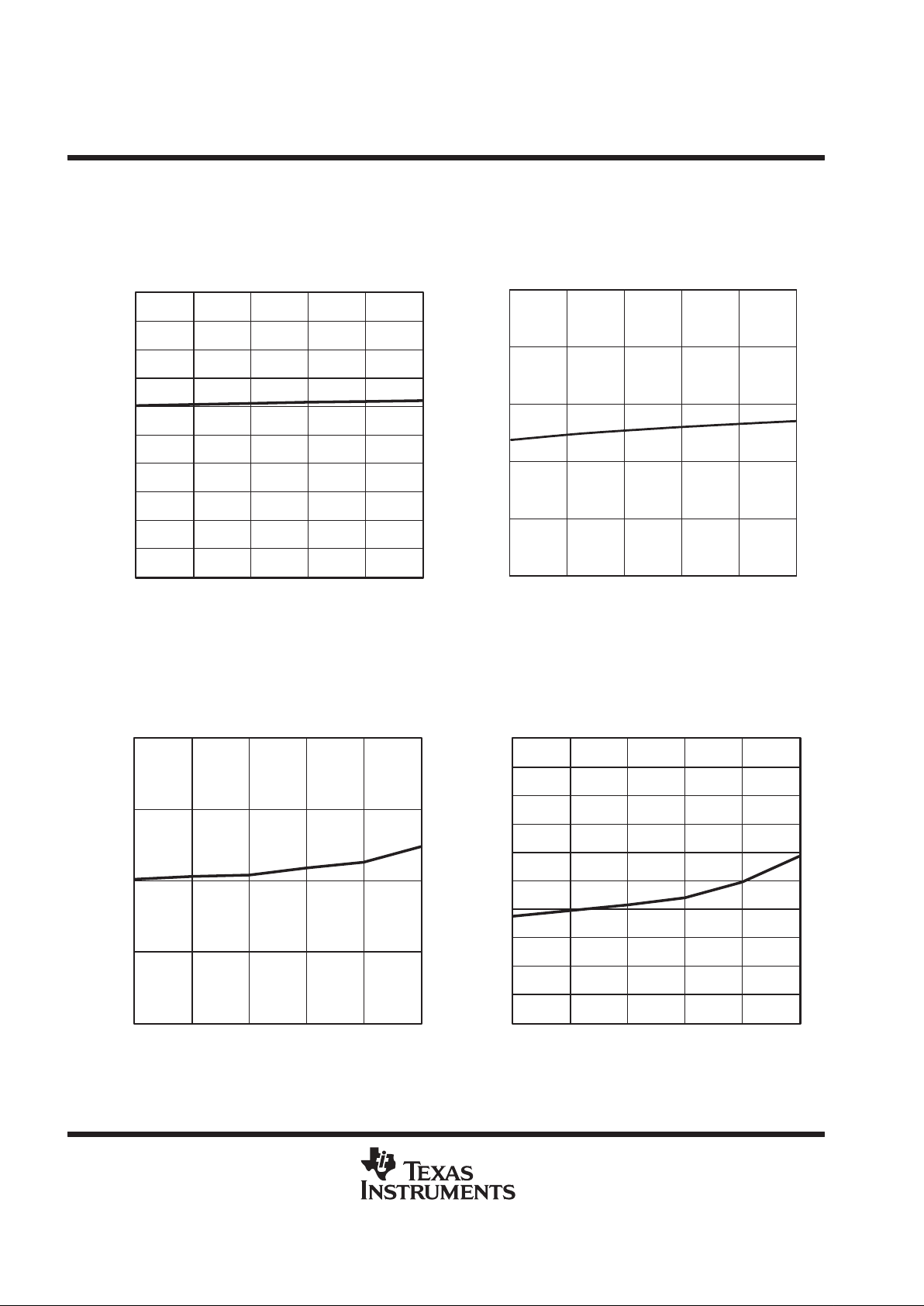
TPS56100
HIGH-EFFICIENCY DSP POWER SUPPLY CONTROLLER
FOR 5-V INPUT SYSTEMS
SLVS201A – JUNE 1999 – REVISED JULY 1999
16
POST OFFICE BOX 655303 • DALLAS, TEXAS 75265
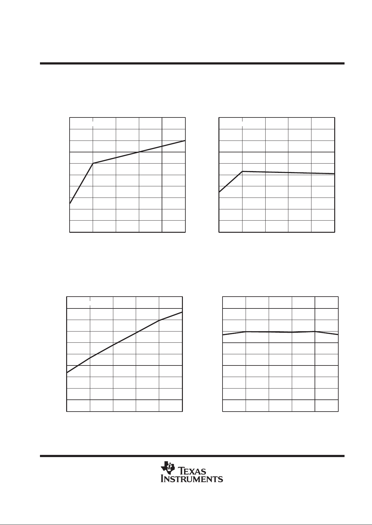
TYPICAL CHARACTERISTICS
Figure 5
113
113.5
114.0
114.5
115.0
115.5
116.0
116.5
117.0
117.5
118.0
0 25 50 75 100 125
OVP Threshold – %
OVP THRESHOLD
vs
JUNCTION TEMPERATURE
TJ – Junction Temperature – °C
Figure 6
TJ – Junction Temperature – °C
OCP THRESHOLD VOLTAGE
vs
JUNCTION TEMPERATURE
99
95
25 75
103
101
97
50 100 125
105
0
OCP Threshold V oltage – mV
Figure 7
1.90
1.95
2.00
2.05
2.10
0 25 50 75 100 125
Inhibit Start Threshold Voltage – V
INHIBIT START THRESHOLD VOLTAGE
vs
JUNCTION TEMPERATURE
TJ – Junction Temperature – °C
Figure 8
100
101
102
103
104
105
106
107
108
109
110
0 25 50 75 100 125
Inhibit Hysteresis Voltage – mV
INHIBIT HYSTERESIS VOLTAGE
vs
JUNCTION TEMPERATURE
TJ – Junction Temperature – °C
TPS56100
HIGH-EFFICIENCY DSP POWER SUPPLY CONTROLLER
FOR 5-V INPUT SYSTEMS
SLVS201A – JUNE 1999 – REVISED JULY 1999
17
POST OFFICE BOX 655303 • DALLAS, TEXAS 75265
TYPICAL CHARACTERISTICS
Figure 9
4.000
4.002
4.004
4.006
4.008
4.010
4.012
4.014
4.016
4.018
4.020
0 25 50 75 100 125
UVLO Start Threshold Voltage – V
UVLO START THRESHOLD VOLTAGE
vs
JUNCTION TEMPERATURE
TJ – Junction Temperature – °C
VI = 5 V
Figure 10
460
461
462
463
464
465
466
467
468
469
470
0 25 50 75 100 125
UVLO Hysteresis – mV
UVLO HYSTERESIS
vs
JUNCTION TEMPERATURE
TJ – Junction Temperature – °C
VI = 5 V
Figure 11
1
1.1
1.2
1.3
1.4
1.5
1.6
1.7
1.8
1.9
2.0
0 25 50 75 100 125
Quiescent Current – mA
QUIESCENT CURRENT
vs
JUNCTION TEMPERATURE
TJ – Junction Temperature – °C
VI = 5 V
Figure 12
92
92.1
92.2
92.3
92.4
92.5
92.6
92.7
92.8
92.9
93.0
0 25 50 75 100 125
Powergood Threshold – %
POWERGOOD THRESHOLD
vs
JUNCTION TEMPERATURE
TJ – Junction Temperature – °C

TPS56100
HIGH-EFFICIENCY DSP POWER SUPPLY CONTROLLER
FOR 5-V INPUT SYSTEMS
SLVS201A – JUNE 1999 – REVISED JULY 1999
18
POST OFFICE BOX 655303 • DALLAS, TEXAS 75265
TYPICAL CHARACTERISTICS
Figure 13
TJ – Junction Temperature – °C
SLOW START CHARGE CURRENT
vs
JUNCTION TEMPERATURE
12
10
25 75
14
13
11
50 100 125
15
0
Slow Start Charge Current – Aµ
V
(VREFB)
= 1.3 V
R
(VREFB)
= 20 kΩ
Figure 14
0
0.5
1.0
1.5
2.0
2.5
3.0
3.5
4.0
0 25 50 75 100 125
DRIVER
HIGH-SIDE OUTPUT RESISTANCE
vs
JUNCTION TEMPERATURE
TJ – Junction Temperature – °C
– High-Side Output Resistance –R
O
Ω
Figure 15
0
1
2
3
4
5
6
7
8
0 25 50 75 100 125
DRIVER
LOW-SIDE OUTPUT RESISTANCE
vs
JUNCTION TEMPERATURE
TJ – Junction Temperature – °C
– Low-Side Output Resistance –R
O
Ω
Figure 16
0
25
50
75
100
125
0 25 50 75 100 125
SENSING SAMPLE/HOLD RESISTANCE
vs
JUNCTION TEMPERATURE
TJ – Junction Temperature – °C
– Sensing Sample/Hold Resistance –R
O
Ω
V
(HISENSE)
= 5 V

TPS56100
HIGH-EFFICIENCY DSP POWER SUPPLY CONTROLLER
FOR 5-V INPUT SYSTEMS
SLVS201A – JUNE 1999 – REVISED JULY 1999
19
POST OFFICE BOX 655303 • DALLAS, TEXAS 75265
APPLICATION INFORMATION
The hysteretic-type controller method used in the TPS56100 controller gives very fast transient response for
today’s high-speed DSP applications. Traditional PWM-type controllers use an oscillator to control the timing
of the control signals used to adjust the output voltage. During a transient load event, the PWM-type controller
must wait until the next oscillator cycle to begin the output voltage adjustment process. This delay causes output
droop (or overshoot) and longer recovery times. Hysteretic-type controllers, such as the TPS56100, are
self-oscillating and require no cycle-time to begin the recovery process. Hysteretic controllers have extremely
high gain and are sensitive to noise. The TPS56100 has internal low-pass noise filters to eliminate much of this
problem, however an external RC low-pass filter between the output and VSENSE input is recommended.
The TPS56100 controller includes all of the functions necessary for a dependable high-efficiency power
converter. High-current synchronous MOSFET drivers are used for fast, low-loss switching allowing for
efficiencies greater than 90%. An internal bootstrap circuit provides the high-side drive voltage necessary for
the upper n-channel MOSFET. Overcurrent protection protects the power supply in case of load faults.
Overvoltage protection protects the load in case of high-side switch failure. Programmable hysteresis allows
users to tailor the output ripple and operating frequency to suit their needs. Slowstart provides a controlled
rampup time for the output voltage eliminating output overshoot. Inhibit is provided for sequencing of the
converter in multiple-voltage circuits. Power good provides an indication that the output voltage is within
operating limits. The design of each of these functions is discussed in detail in the following. Refer to Figure 19
for location of components discussed in the following.

TPS56100
HIGH-EFFICIENCY DSP POWER SUPPLY CONTROLLER
FOR 5-V INPUT SYSTEMS
SLVS201A – JUNE 1999 – REVISED JULY 1999
20
POST OFFICE BOX 655303 • DALLAS, TEXAS 75265
APPLICATION INFORMATION
frequency calculation
A detailed derivation of frequency calculation is shown in the application report,
Designing Fast Response
Synchronous Buck Regulators Using the TPS5210
, TI Literature number SL VA044. When less accurate results
are acceptable, the simplified equation shown below can be used:
fs≅
ǒ
VO ƪVI*
V
O
ƫ
ESR
Ǔ
ǒ
VI L
Hysteresis Window
Ǔ
control section
Below are the equations needed to select the various components within the control section. Component
reference numbers refer to the example application given at the end of this section. Details and the derivations
of the equations used in this section are available in the application report
Designing Fast Response
Synchronous Buck Regulators Using the TPS5210
, TI Literature number SLVA044.
output voltage selection
Of course the most important function of the power supply is to regulate the output voltage to a specific value.
Values between 1.3 V and 2.6 V can be easily set by shorting the correct VP inputs to ground. Values above
the maximum reference voltage (2.6 V) can be set by changing the reference voltage to any convenient voltage
within its range and selecting values for R2 and R3 to give the correct output. Select R3:
R3 << than V
REF/IBIAS(VSENSE)
; a recommended value is 10 kΩ
Then, calculate R2 using:
VO+
V
REF
ǒ
1
)
R2
R3
Ǔ
or R2
+
R3
ǒVO*
V
REF
Ǔ
V
REF
R2 and R3 can also be used to make small adjusts to the output voltage within the reference-voltage range.
If there is no need to adjust the output voltage, R3 can be eliminated. R2, R3 (if used), and C7 are used as a
noise filter; calculate using:
C7
+
150 ns
ǒ
R2øR3
Ǔ
Recommended values for 3.3 V: V
REF
= 1.65 V, R3 = 1.00 kΩ, R2 = 1.00 kΩ, and C7 = 100 pF.
slowstart timing
Slowstart reduces the start-up stresses on the power-stage components and reduces the input current surge.
Slowstart timing is a function of the reference-voltage current (determined by R5) and is independent of the
reference voltage. The first step in setting slowstart timing will be to determine R5:
R5 should be between 7 kΩ and 300 kΩ, a recommended value is 20 kΩ.
TPS56100
HIGH-EFFICIENCY DSP POWER SUPPLY CONTROLLER
FOR 5-V INPUT SYSTEMS
SLVS201A – JUNE 1999 – REVISED JULY 1999
21
POST OFFICE BOX 655303 • DALLAS, TEXAS 75265
APPLICATION INFORMATION
slowstart timing (continued)
Set the slowstart timing using the formula:
C5
+
t
ss
ǒ
5 R
VREFB
Ǔ
≅
t
ss
(
5 R5
)
Where
C5 = Slowstart capacitance in µF
tSS = Slowstart timing in µs
R
VREFB
= Resistance from VREFB to GND in ohms (≈ R5)
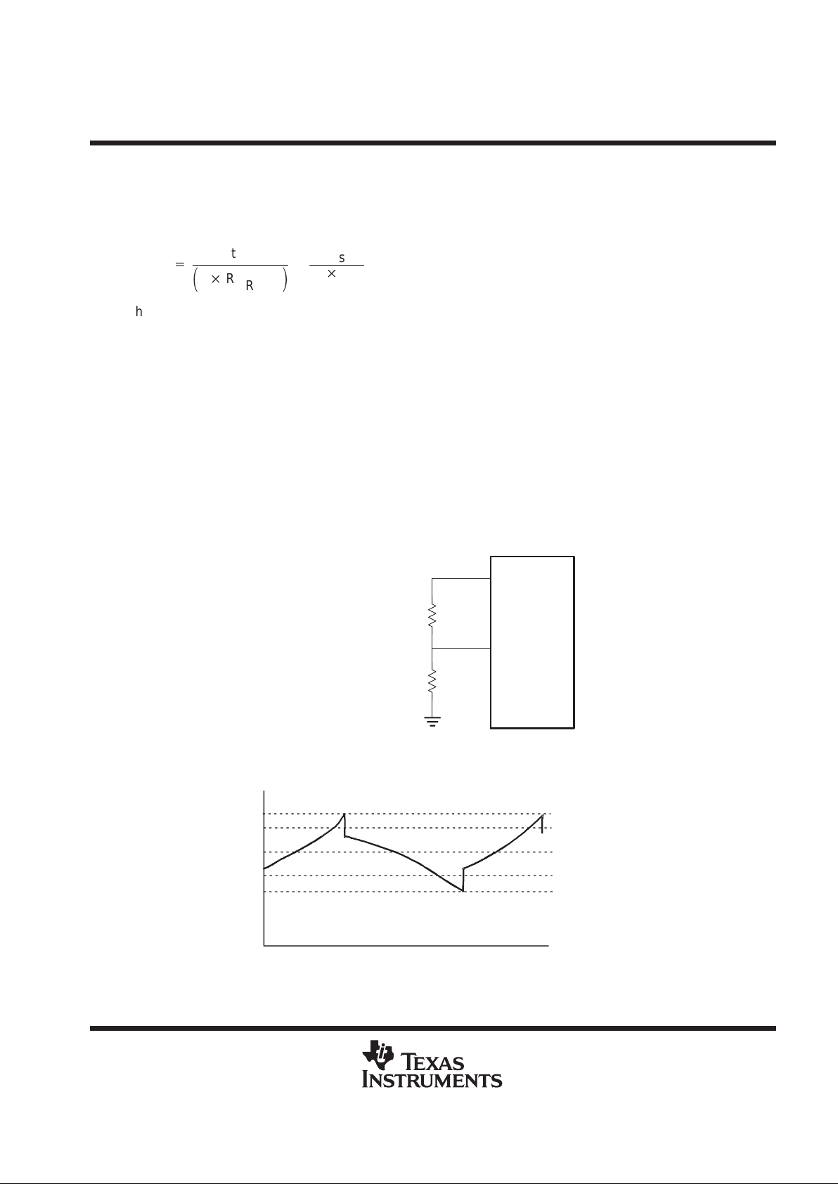
hysteresis voltage
A hysteretic controller regulates by self-oscillation, thus requiring a small ripple voltage on the output which the
input comparator uses for sensing. Once selected, the TPS56100 hysteresis is proportional to the reference
voltage; programming Vref to a new value automatically adjusts the hysteresis to be the same percentage of
Vref. The actual output ripple voltage is the combination of the hysteresis voltage, overshoot caused by internal
delays, and the output capacitor characteristics. Figure 19 shows the hysteresis window voltage (VHI to VLO)
and the output voltage ripple (V
MAX
to V
MIN
). Since the output current from VREFB should be less than
500 µA, the total divider resistance (R4 + R5) should be greater than 7 kΩ. The hysteresis voltage should be
no greater than 60 mV so R5 will dominate the divider.
R4
R5
VHSYT
VREFB
Hysteresis Window = 2 × V
R4
Figure 17. Hysteresis Divider Circuit
V
O
V
MAX
V
MIN
V
REF
V
HI
V
LO
t
Figure 18. Output Ripple

TPS56100
HIGH-EFFICIENCY DSP POWER SUPPLY CONTROLLER
FOR 5-V INPUT SYSTEMS
SLVS201A – JUNE 1999 – REVISED JULY 1999
22
POST OFFICE BOX 655303 • DALLAS, TEXAS 75265
APPLICATION INFORMATION
hysteresis voltage (continued)
The upper divider resistor, R4, is calculated using:
R4
+
Hysteresis Window
2 (VREFB*Hysteresis Window
)
R5 ≅
V
HYST
(%)
(
2 100
)
R5
Where
Hysteresis Window = the desired peak-to-peak hysteresis voltage.
VREFB = selected reference voltage.
V
HYST
(%) = [(Hysteresis Window)/VREFB] * 100 < V
O(Ripple)(P-P)
(%)
current limit
Current limit can be implemented using the on-resistance of the upper FET s as the sensing element. Select R7:
R7
Ơ
V
OCP
I
Bias(OCP)
≤
0.1 V
(
100 100 nA
)
≤ 10 kΩ (A recommended value is 1 kΩ)
The IOUT signal is used to drive the current limit divider. The voltage at IOUT at the output current trip point will
be:
V
IOUT(Trip)
+
ǒ
2 R
DS(ON)
TF
Ǔ
NumFETs
I
O(Trip)
Where
NumFETS = Number of upper FETS in Parallel.
TF = R
DS(ON)
temperature correction factor.
I
O(Trip)
= Desired output current trip level (A).
Calculate R6 using:
R6
+
ǒ
V
IOUT(Trip)
0.1 V
*
1Ǔ
R7
Note that since R
DS(ON)
of MOSFET s can vary from lot to lot and with temperature, tight current-limit control (less
than 1.5 x IO) using this method is not practical. If tight control is required, an external current-sense resistor
in series with the drain of the upper FET can be used with HISENSE and LOSENSE connected across the
resistor.

TPS56100
HIGH-EFFICIENCY DSP POWER SUPPLY CONTROLLER
FOR 5-V INPUT SYSTEMS
SLVS201A – JUNE 1999 – REVISED JULY 1999
23
POST OFFICE BOX 655303 • DALLAS, TEXAS 75265
APPLICATION INFORMATION
application example
Below is a typical application schematic. The circuit can be divided into the power-stage section and the
control-circuit section. The power stage must be tailored to the input/output requirements of the application. The
control circuit is basically the same for all applications with some minor tweaking of specific values.
15
VCC
14
DRV
21
IOUTLO
22
INHIBIT
17
HIGHDR
16
BOOT
20
LOSENSE
8
SLOWST
7
ANAGND
9
BIAS
19
HISENSE
18
BOOTLO
13
LOWDR
12
DRVGND
11
LOHIB
10
LODRV
1
IOUT
28
PWRGD
5
VREFB
6
VSENSE
4
VHYST
3
OCP
27
VP0
26
VP1
25
VP2
24
VP3
23
VP4
2
NC
TPS56100
U1
C6
0.033 uF
C3
1 uF
10
R1
GND
R101
Q101
L101
C103C102
+
C101
Q102
5V
5V
Power Stage
Control Section
+
C105
C106
Vo
L102
R102
C104
RTN
1 uF
C2
R6
3.92 k
1.00 k
R7
10.0 kR3
C7
1000 pF
100
R4
20.0 k
R5
C5
0.1 uF
C4
1 uF
R2
150
HIGHDRV
HISENSE
LOSENSE
BOOTLO
DRVGND
LOHIB
LOWDR
VSENSE
RTN
NOTE A: VP0 – VP4 are user slected
to set output voltage.
C1 is deleted.
Figure 19. Typical Application Schematic

TPS56100
HIGH-EFFICIENCY DSP POWER SUPPLY CONTROLLER
FOR 5-V INPUT SYSTEMS
SLVS201A – JUNE 1999 – REVISED JULY 1999
24
POST OFFICE BOX 655303 • DALLAS, TEXAS 75265
APPLICATION INFORMATION
application example (continued)
Table 2. Power Stage Components
Ref Des Function 4–A Out 8–A Out 12–A Out 20–A Out
C101 Input Bulk
Capacitor
Sanyo,
10TPB220M,
220–µF, 10–V, 20%
Sanyo,
10SA220M,
2 x 220–µF, 10–V, 20%
Sanyo,
10SP470M,
2 x 470–µF, 10–V, 20%
Sanyo,
10SP470M,
3 x 470–µF, 10–V, 20%
C102 Input Mid–Freq
Capacitor
muRata,
GRM42–6Y5V105Z025A,
1.0–µF, 25–V,
+80%–20%, Y5V
muRata,
GRM42–6Y5V225Z016A,
2.2–µF, 16–V,
+80%–20%, Y5V
muRata,
GRM42–6Y5V225Z016A,
2.2–µF, 16–V, +80%–20%,
Y5V
muRata,
GRM42–6Y5V105Z025A,
3 x 1.0–µF, 25–V,
+80%–20%, Y5V
C103 Input Hi–Freq
Bypass
Capacitor
muRata,
GRM39X7R104K016A,
0.1–µF, 16–V, X7R
muRata,
GRM39X7R104K016A,
0.1–µF, 16–V, X7R
muRata,
GRM39X7R104K016A,
2 x 0.1–µF, 16–V, X7R
muRata,
GRM39X7R104K016A,
3 x 0.1–µF, 16–V, X7R
C104 Snubber
Capacitor
muRata,
GRM39X7R102K050A,
1000–pF, 50–V, X7R
muRata,
GRM39X7R102K050A,
1000–pF, 50–V, X7R
muRata,
GRM39X7R102K050A,
2 x 1000 pF, 50–V, X7R
muRata,
GRM39X7R102K050A,
3 x 1000–pF, 50–V, X7R
C105 Output Bulk
Capacitor
Sanyo,
4TPC150,
2 x 150–µF, 4–V, 20%
Sanyo,
4SP820M,
820–µF, 4–V, 20%
Sanyo,
4SP820M,
2 x 820–µF, 4–V, 20%
Sanyo,
4SP820M,
3 x 820–µF, 4–V, 20%
C106 Output Hi–Freq
Bypass Capacitor
muRata,
GRM39X7R104K016A,
0.1–µF, 16–V, X7R
muRata,
GRM39X7R104K016A,
0.1–µF, 16–V, X7R
muRata,
GRM39X7R104K016A,
2 x 0.1–µF, 16–V, X7R
muRata,
GRM39X7R104K016A,
3 x 0.1–µF, 16–V, X7R
L101 Input Filter
Inductor
CoilCraft,
DO1608C–332,
3.3–µH, 2.0–A
Coiltronics,
UP2B–2R2,
2.2–µH, 7.2–A
Coiltronics,
UP2B–2R2,
2.2–µH, 7.2–A
Coiltronics,
UP3B–1R0,
1–µH, 12.5–A
L102 Output Filter
Inductor
CoilCraft,
DO3316P–332,
3.3–µH, 6.1–A
Coiltronics,
UP3B–2R2,
2.2–µH, 9.2–A
Coiltronics,
UP4B–1R5,
1.5–µH, 13.4–A
MicroMetals,
T68–8/90 Core w/7T #16,
1.0–µH, 25–A
R101 Lo–Side Gate
Resistor
3.3–Ω, 1/16–W, 5% 3.3–Ω, 1/16–W, 5% 2 x 3.3–Ω, 1/16–W, 5% 3 x 3.3–Ω, 1/16–W, 5%
R102 Snubber
Resistor
2.7–Ω, 1/10–W, 5% 2.7–Ω, 1/10–W, 5% 2 x 2.7–Ω, 1/10–W, 5% 3 x 2.7–Ω, 1/10–W, 5%
Q101 Power Switch IR, IRF7811,
NMOS, 11–mΩ
IR, IRF7811,
NMOS, 11–mΩ
IR, 2 x IRF7811, NMOS,
11–mΩ
IR, 2 x IRF7811, NMOS,
11–mΩ
Q102 Synchronous
Switch
IR, IRF7811,
NMOS, 11–mΩ
IR, IRF7811,
NMOS, 11–mΩ
IR, 2 x IRF7811, NMOS,
11–mΩ
IR, 3 x IRF7811, NMOS,
11–mΩ
Nominal Frequency
†
280 kHz 250 kHz 170 kHz 170 kHz
Hysteresis Window 15 mV 15 mV 15 mV 15 mV
†
Nominal frequency measured with Vo set to 1.5 V.
The values listed above are recommendations based on actual test circuits. Many variations of the above are
possible based upon the desires and/or requirements of the user. Performance of the circuit is equally, if not
more, dependent upon the layout than on the specific components, as long as the device parameters are not
exceeded. Fast-response, low-noise circuits require critical attention to the layout details. Even though the
operating frequencies of typical power supplies are relatively low compared to today’s microprocessor circuits,
the power levels and edge rates can cause severe problems both in the supply and the load. The power stage,
having the highest current levels and greatest dv/dt rates, should be given the greatest attention.

TPS56100
HIGH-EFFICIENCY DSP POWER SUPPLY CONTROLLER
FOR 5-V INPUT SYSTEMS
SLVS201A – JUNE 1999 – REVISED JULY 1999
25
POST OFFICE BOX 655303 • DALLAS, TEXAS 75265
APPLICATION INFORMATION
layout guidelines
Good power supply results will only occur when care is given to proper design and layout. Layout will affect noise
pickup and generation and can cause a good design to perform with less than expected results. With a range
of currents from milliamps to tens or even hundreds of amps, good power supply layout is much more difficult
than most general PCB designs. The general design should proceed from the switching node to the output, then
back to the driver section and, finally, place the low-level components. Below are several specific points to
consider
before
layout of a TPS56100 design begins.
1. All sensitive analog components should be referenced to ANAGND. These include components connected
to SLOWST, IOUT, OCP, VSENSE, VREFB, VHYST, BIAS, and LOHIB.
2. Analog ground and drive ground should be isolated as much as possible. Ideally , analog ground will connect
to the ground side of the bulk storage capacitors on V
O
, and drive ground will connect to the main ground
plane close to the source of the low-side FET.
3. Connections from the drivers to the gate of the power FETs should be as short and wide as possible to
reduce stray inductance. This becomes more critical if external gate resistors are not being used.
4. The bypass capacitor for the DRV input should be placed close to the TPS56100 and be connected to
DRVGND.
5. The bypass capacitor for VCC should be placed close to the TPS56100 and be connected to AGND.
6. When configuring the high-side driver as a floating driver , the connection from BOOTLO to the power FET s
should be as short and as wide as possible. The other pins that also connect to the power FETs, LOHIB
and LOSENSE, should have a separate connection to the FETS since BOOTLO will have large peak
currents flowing through it.
7. When configuring the high-side driver as a floating driver , the bootstrap capacitor (connected from BOOT
to BOOTLO) should be placed close to the TPS56100.
8. When configuring the high-side driver as a ground-referenced driver, BOOTLO should be connected to
DRVGND.
9. The bulk storage capacitors across V
I
should be placed close to the power FETS. High-frequency bypass
capacitors should be placed in parallel with the bulk capacitors and connected close to the drain of the
high-side FET and to the source of the low-side FET.
10. High-frequency bypass capacitors should be placed across the bulk storage capacitors on VO.
11. HISENSE and LOSENSE should be connected very close to the drain and source, respectively, of the
high-side FET. HISENSE and LOSENSE should be routed very close to each other to minimize
differential-mode noise coupling to these traces. Ceramic decoupling capacitors should be placed close to
where HISENSE connects to Vin, to reduce high-frequency noise coupling on HISENSE.

TPS56100
HIGH-EFFICIENCY DSP POWER SUPPLY CONTROLLER
FOR 5-V INPUT SYSTEMS
SLVS201A – JUNE 1999 – REVISED JULY 1999
26
POST OFFICE BOX 655303 • DALLAS, TEXAS 75265
MECHANICAL DATA
PWP (R-PDSO-G**) PowerPAD PLASTIC SMALL-OUTLINE PACKAGE
4073225/E 03/97
0,50
0,75
0,25
0,15 NOM
Thermal Pad
(See Note D)
Gage Plane
2824
7,70
7,90
20
6,40
6,60
9,60
9,80
6,60
6,20
11
0,19
4,50
4,30
10
0,15
20
A
1
0,30
1,20 MAX
1614
5,10
4,90
PINS **
4,90
5,10
DIM
A MIN
A MAX
0,05
Seating Plane
0,65
0,10
M
0,10
0°–8°
20-PIN SHOWN
NOTES: B. All linear dimensions are in millimeters.
C. This drawing is subject to change without notice.
D. Body dimensions do not include mold flash or protrusions.
E. The package thermal performance may be enhanced by bonding the thermal pad to an external thermal plane. This pad is electrically
and thermally connected to the backside of the die and possibly selected leads.
F. Falls within JEDEC MO-153
PowerPAD is a trademark of Texas Instruments Incorporated.

IMPORTANT NOTICE
T exas Instruments and its subsidiaries (TI) reserve the right to make changes to their products or to discontinue
any product or service without notice, and advise customers to obtain the latest version of relevant information
to verify, before placing orders, that information being relied on is current and complete. All products are sold
subject to the terms and conditions of sale supplied at the time of order acknowledgement, including those
pertaining to warranty, patent infringement, and limitation of liability.
TI warrants performance of its semiconductor products to the specifications applicable at the time of sale in
accordance with TI’s standard warranty. Testing and other quality control techniques are utilized to the extent
TI deems necessary to support this warranty. Specific testing of all parameters of each device is not necessarily
performed, except those mandated by government requirements.
CERT AIN APPLICATIONS USING SEMICONDUCTOR PRODUCTS MAY INVOL VE POTENTIAL RISKS OF
DEATH, PERSONAL INJURY, OR SEVERE PROPERTY OR ENVIRONMENTAL DAMAGE (“CRITICAL
APPLICATIONS”). TI SEMICONDUCTOR PRODUCTS ARE NOT DESIGNED, AUTHORIZED, OR
WARRANTED TO BE SUITABLE FOR USE IN LIFE-SUPPORT DEVICES OR SYSTEMS OR OTHER
CRITICAL APPLICATIONS. INCLUSION OF TI PRODUCTS IN SUCH APPLICA TIONS IS UNDERSTOOD T O
BE FULLY AT THE CUSTOMER’S RISK.
In order to minimize risks associated with the customer’s applications, adequate design and operating
safeguards must be provided by the customer to minimize inherent or procedural hazards.
TI assumes no liability for applications assistance or customer product design. TI does not warrant or represent
that any license, either express or implied, is granted under any patent right, copyright, mask work right, or other
intellectual property right of TI covering or relating to any combination, machine, or process in which such
semiconductor products or services might be or are used. TI’s publication of information regarding any third
party’s products or services does not constitute TI’s approval, warranty or endorsement thereof.
Copyright 1999, Texas Instruments Incorporated
 Loading...