

Texas Instruments TPS5602IDBR, TPS5602IDBT, TPS5602EVM-121 Datasheet
TPS5602
DUAL, FAST, HIGH EFFICIENCY CONTROLLER FOR DSP POWER
SLVS217 – JUNE 1999
1
POST OFFICE BOX 655303 • DALLAS, TEXAS 75265
D
Independent Dual Channels
D
Hysteretic Control for Fast Transient
Response
D
4.5-V to 25-V Input Voltage Range
D
Adjustable Output Voltage Down to 1.2 V
D
Synchronous Rectifier Enables Efficiencies
of >95%
D
Minimized External Component Count
D
Separate Standby Control and Over Current
Protection
D
Low Supply Current...0.8 mA Typ
D
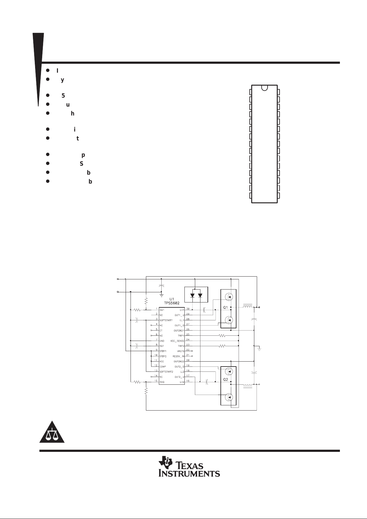
30-Pin TSSOP
D
Low Standby Current (1-µA maximum)
D
EVM Available (TPS5602EVM-121)
description
The TPS5602 is a dual-channel synchronous
buck switch-mode power supply controller
featuring very fast feedback control and minimized component count. By using the hysteretic control method,
it is ideal for high-transient current applications, such as ’C6000 and multiple ’C54x DSPs. The TPS5602 is
designed specifically for DSP applications that require high efficiency. Since both channels are independent,
the up and down power sequencing can be easily achieved by properly setting the standby pins. The wide input
voltage and adjustable output voltage make the TPS5602 suitable for many applications.
typical design
R4
R1
+
C3
R3
R2
D1
C2
C1
GND
5 V
C7
L1
C4
R5
R6
OUT2
C8
L2
C5
OUT1
1.8 V
3.3 V
Copyright 1999, Texas Instruments Incorporated
PRODUCTION DATA information is current as of publication date.
Products conform to specifications per the terms of Texas Instruments
standard warranty. Production processing does not necessarily include
testing of all parameters.
Please be aware that an important notice concerning availability, standard warranty, and use in critical applications of
Texas Instruments semiconductor products and disclaimers thereto appears at the end of this data sheet.
1
2
3
4
5
6
7
8
9
10
11
12
13
14
15
30
29
28
27
26
25
24
23
22
21
20
19
18
17
16
INV1
NC
SOFTSTAR T1
NC
C
T
NC
GND
REF
STBY1
STBY2
V
CC
COMP
SOFTSTAR T2
NC
INV2
LH1
OUT1_u
LL1
OUT1_d
OUTGND1
TRIP1
V
CC
SENSE
TRIP2
Vref5
REG5V_IN
OUTGND2
OUT2_d
LL2
OUT2_u
LH2
DBT PACKAGE
(TOP VIEW)
NC – No internal connection
TPS5602
DUAL, FAST, HIGH EFFICIENCY CONTROLLER FOR DSP POWER
SLVS217 – JUNE 1999
2
POST OFFICE BOX 655303 • DALLAS, TEXAS 75265
AVAILABLE OPTIONS
PACKAGE
T
A
TSSOP
(DBT)
EVM
°
°
TPS5602IDBT
–
40°C to 85°C
TPS5602IDBTR
TPS5602EVM-121
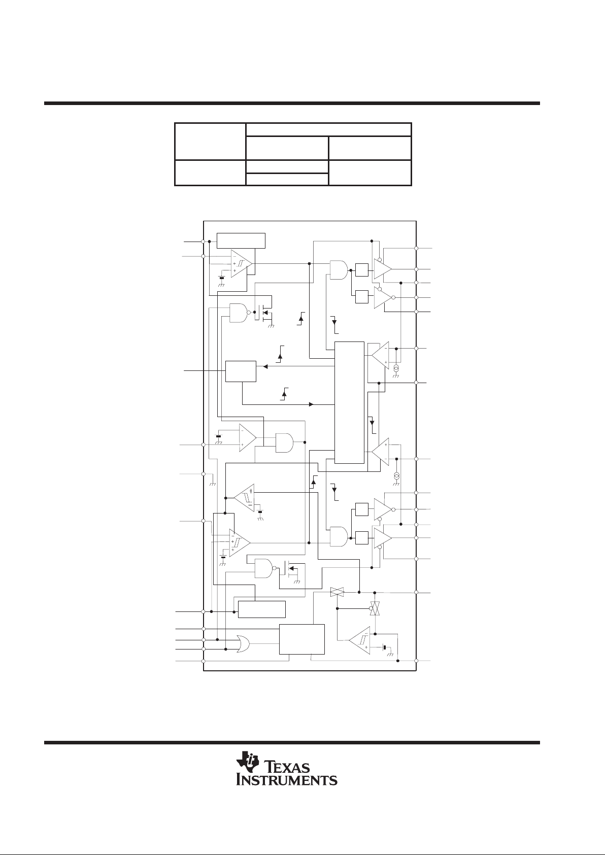
functional block diagram
4.5 V
OUTGND2
Comp
Hysteretic Comp.
Current Comp.
VREF5
Current Comp.
LH1
LL1
OUT1_d
OUT1_u
OUTGND1
TRIP1
TRIP2
OUT2_d
LL2
Out2_u
LH2
VccSENSE
REG5Vin
SFT1
SOFT START2
INV1
INV2
Vref
Vcc
STBY1
STBY2
UVLO
GND
SOFT START1
1.1 V
REF
OSC
1.185 V
1.185 V
Current
Protection
Trigger
SFT2
Setup trigger
Setup trigger
Trigger on
OSC on
Fixed off–time reset
1.185 V
DLY
3.8 V
Hysteretic Comp. DLY
DLY
DLY
C
T
TPS5602
DUAL, FAST, HIGH EFFICIENCY CONTROLLER FOR DSP POWER
SLVS217 – JUNE 1999
3
POST OFFICE BOX 655303 • DALLAS, TEXAS 75265
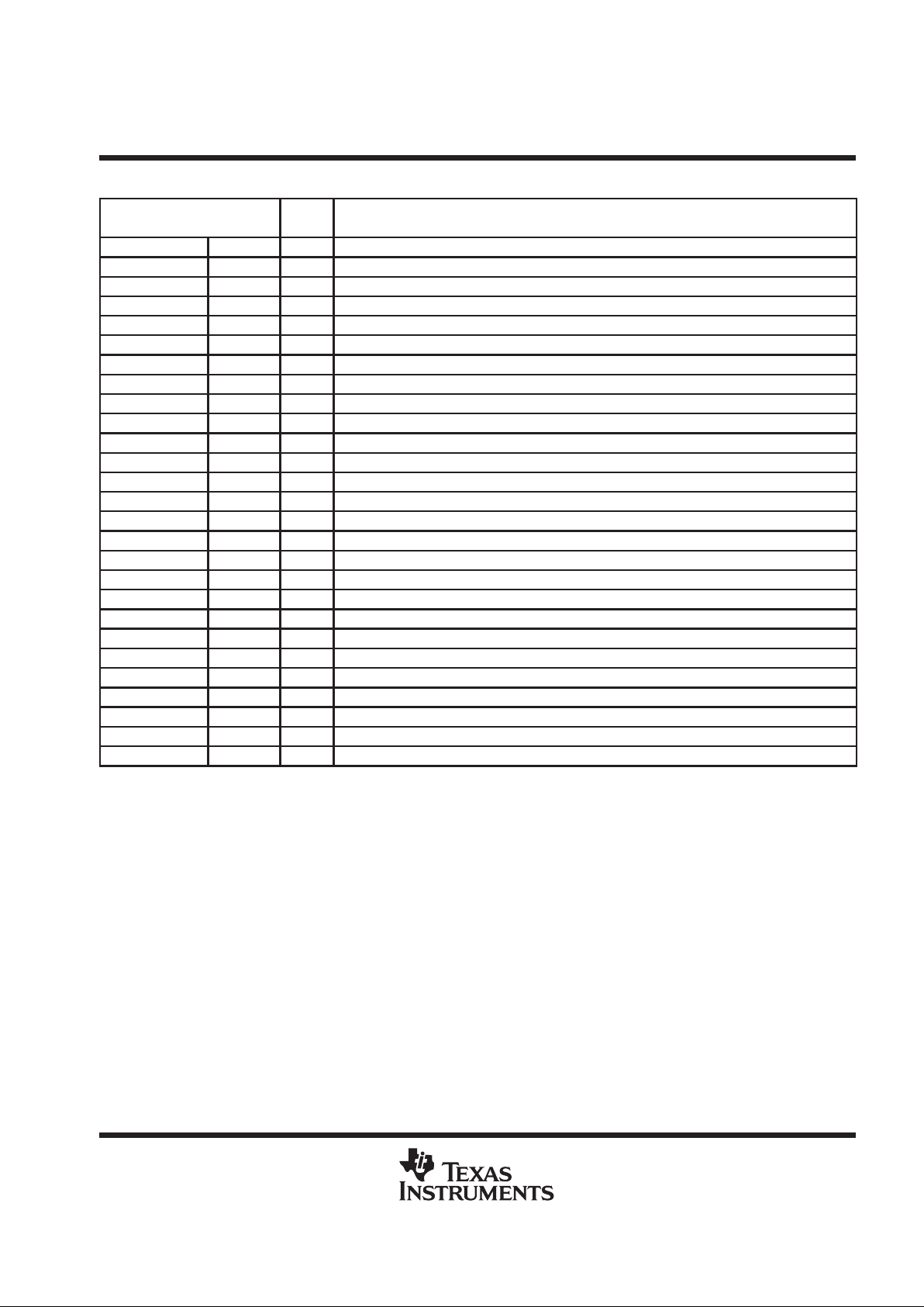
Terminal Functions
TERMINAL
NAME NO.
I/O
DESCRIPTION
COMP 12 I/O Voltage monitor comparator input
C
T
5 I/O The oscillator frequency external capacitor connection
GND 7 Control GND
INV1 1 I CH1 hysteretic comparator inverting input
INV2 15 I CH2 hysteretic comparator inverting input
LH1 30 I/O CH2 high-side gate drive boost capacitor input
LH2 16 I/O CH1 high-side gate drive boost capacitor input
LL1 28 I/O CH1 high-side drive and current protection
LL2 18 I/O CH2 high-side drive and current protection
NC 2, 4, 6, 14
OUT1_d 27 I/O CH1 low-side gate drive output
OUT2_d 19 O CH2 low-side gate drive output
OUT1_u 29 O CH1 high-side switch output
OUT2_u 17 O CH2 high-side switch output
OUTGND1 26 Output GND 1
OUTGND2 20 Output GND 2
REF 8 O 1.185-V reference voltage output
REG5V_IN 21 I External 5-V input
SOFTSTAR T1 3 I/O CH1 soft start control external capacitor connection
SOFTSTAR T2 13 I/O CH2 soft start control external capacitor connection
STBY1 9 I CH1 standby control
STBY2 10 I CH2 standby control
TRIP1 25 I CH1 output current control input
TRIP2 23 I CH2 output current control input
V
CC
11 I Supply voltage input
Vref5 22 O 5-V internal regulator output
VCCSENSE 24 I Supply voltage sense input
detailed description
vref (1.185 V)
The reference voltage is used for the output voltage setting and the voltage protection (COMP).
vref (5 V)
An internal linear voltage regulator offers a fixed 5-V voltage as the bootstrap voltage so that the design for the
bootstrap is much easier. The tolerance is 6%. The extra current capability can also be used to power external
circuitry .
5-V switch
If the internal 5-V switch senses a 5-V input from REG5V pin, the internal 5-V linear regulator will be
disconnected from the MOSFET drivers. The external 5-V will be used for the low-side driver and the high-side
bootstrap, thus increasing the efficiency.
TPS5602
DUAL, FAST, HIGH EFFICIENCY CONTROLLER FOR DSP POWER
SLVS217 – JUNE 1999
4
POST OFFICE BOX 655303 • DALLAS, TEXAS 75265
detailed description (continued)
hysteretic comparator
Each channel has a hysteretic comparator to regulate the output voltage of the synchronous-buck converter.
The hysteresis is set internally and is typically 8.5 mV. The total delay from the comparator input to the driver
output is typically 500 ns from low to high and 350 ns from high to low.
low-side driver
The low-side driver is designed to driver low-Rds(on) n-channel MOSFET s. The maximum drive voltage is 5V
from Vref5. The current rating of the driver is typically 1 A, source and sink.
high-side driver
The high side driver is designed to drive low-Rds(on) n-channel MOSFETs. The current rating of the driver is
1 A, source and sink. When configured as a floating driver, the bias voltage to the driver is developed from the
Vref5, limiting the maximum drive voltage between OUTxU and LLx to 5 V. The maximum voltage that can be
applied between LHx and OUTGNDx is 30 V.
deadtime control
Deadtime control prevents shoot-through current from flowing through the main power FETs during switching
transitions by actively controlling the turnon time of the MOSFETs drivers. The typical deadtime from
low-side-driver-off to high-side-driver-on is 75 ns and 164 ns from high-side-driver-off to low-side-driver-on.
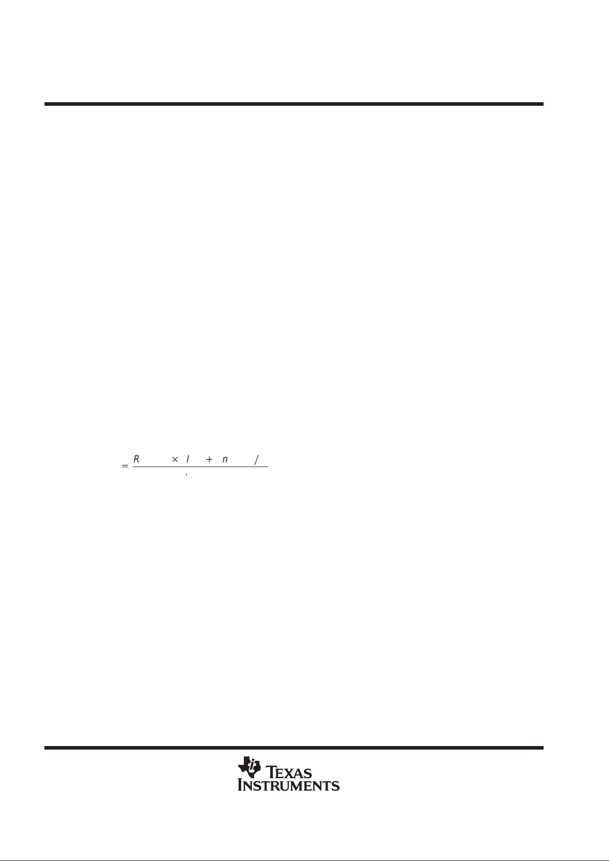
current protection
The current protection is achieved by sensing the high-side power MOSFET drain-to-source voltage drop during
on-time through V
CC
Sense and LLx pins. An external resistor between Vin and TRIPx pin with the internal
current source connected to the current comparator negative input adjusts the current limit. The typical internal
current source current is 15 µA. When the voltage on the positive pin is lower than the negative pin, the current
comparator turns on the trigger, and then activates the oscillator. This oscillator repeatedly resets the trigger
until the overcurrent condition is removed. The equation for the external resistor selection is:
Rclmt
+
Rds(on
) (
Itrip)Iind(p-p
)ń2)
0.000015
Where Rds(on) is the MOSFET turnon resistance; Itrip is the required trip current; Iind(p-p) is the peak-to-peak
inductor ripple current. Itrip must be greater than 0.5×Iind(p-p). The tolerance is ±30%.
COMP
COMP is an internal comparator used for any voltage protection such as the output under-voltage protection
for DSP power applications. If the core voltage is lower than the setpoint, the comparator turns off both channels
to prevent the DSP from damage.
SOFT1, SOFT2
Separate soft-start terminals make it possible to set the sequencing of each output for any possibility. The
capacitor value for a start-up time can be calculated by the following equation:
C = 2 × T (µF)
Where C is the external capacitor value, T is the required start-up time in (ms).
STBY1, STBY2
Both channels can be switched into standby mode separately by grounding the STBY pin. The standby current
is less than 1 µA. The STBY pins can be used for sequencing.
UVLO
When the input voltage rises to about 3.8 V , the IC is turned on, ready to function. When the input voltage falls
below the turnon value, the IC is turned off. The typical hysteresis is 149 mV.
TPS5602
DUAL, FAST, HIGH EFFICIENCY CONTROLLER FOR DSP POWER
SLVS217 – JUNE 1999
5
POST OFFICE BOX 655303 • DALLAS, TEXAS 75265
absolute maximum ratings over operating free-air temperature (see Note 1) (unless otherwise
noted)
†
Supply voltage, V
CC
–0.3 V to 27 V. . . . . . . . . . . . . . . . . . . . . . . . . . . . . . . . . . . . . . . . . . . . . . . . . . . . . . . . . . . . . .
Input voltage, V
I
, INV –0.3 V to 7 V. . . . . . . . . . . . . . . . . . . . . . . . . . . . . . . . . . . . . . . . . . . . . . . . . . . . . . . . . . . . . . .
Softstart –0.3 V to 7 V. . . . . . . . . . . . . . . . . . . . . . . . . . . . . . . . . . . . . . . . . . . . . . . . . . . . . . . . . . .
COMP –0.3 V to 6 V. . . . . . . . . . . . . . . . . . . . . . . . . . . . . . . . . . . . . . . . . . . . . . . . . . . . . . . . . . . .
REG5V_IN –0.3 V to 6 V. . . . . . . . . . . . . . . . . . . . . . . . . . . . . . . . . . . . . . . . . . . . . . . . . . . . . . . .
STBY –0.3 V to 15 V. . . . . . . . . . . . . . . . . . . . . . . . . . . . . . . . . . . . . . . . . . . . . . . . . . . . . . . . . . . .
TRIP –0.3 V to 15 V. . . . . . . . . . . . . . . . . . . . . . . . . . . . . . . . . . . . . . . . . . . . . . . . . . . . . . . . . . . . .
Maximum Driver current 3 A. . . . . . . . . . . . . . . . . . . . . . . . . . . . . . . . . . . . . . . . . . . . . . . . . . . . . . . . . . . . . . . . . . . . .
Output voltage, LLx –0.3 V to 27 V. . . . . . . . . . . . . . . . . . . . . . . . . . . . . . . . . . . . . . . . . . . . . . . . . . . . . . . . . . . . . . .
Output voltage, OUTx_u –0.3 V to 32 V. . . . . . . . . . . . . . . . . . . . . . . . . . . . . . . . . . . . . . . . . . . . . . . . . . . . . . . . . . .
Output voltage, OUTx_d –0.3 V to 7 V. . . . . . . . . . . . . . . . . . . . . . . . . . . . . . . . . . . . . . . . . . . . . . . . . . . . . . . . . . . .
Power dissipation (T
A
= 25°C) See Dissipation Table. . . . . . . . . . . . . . . . . . . . . . . . . . . . . . . . . . . . . . . . . . . . . . . .
Operating free-air temperature range, T
A
–40°C to 85°C. . . . . . . . . . . . . . . . . . . . . . . . . . . . . . . . . . . . . . . . . . . .
Operating virtual junction temperature range, T
J
125°C. . . . . . . . . . . . . . . . . . . . . . . . . . . . . . . . . . . . . . . . . . . . .
Storage temperature range, T
stg
–55°C to 150°C. . . . . . . . . . . . . . . . . . . . . . . . . . . . . . . . . . . . . . . . . . . . . . . . . . .
†
Stresses beyond those listed under “absolute maximum ratings” may cause permanent damage to the device. These are stress ratings only, and
functional operation of the device at these or any other conditions beyond those indicated under “recommended operating conditions” is not
implied. Exposure to absolute-maximum-rated conditions for extended periods may affect device reliability.
NOTE 1: All voltages are with respect to GND terminal.
DISSIPATION RATING TABLE
PACKAGE
TA = 25°C
POWER DISSIPATION
TA ≥ 25°C
DERATING FACTOR
TA = 85°C
POWER DISSIPATION
DBT 874 mW 6.993 mW/°C 454 mW
recommended operating conditions
MIN NOM MAX UNIT
Supply voltage, V
CC
4.5 25 V
INV1/2 6
COMP 6
SOFTSTART1/2 6
Input voltage, V
I
REG5V_IN 5.5
V
STBY1/STBY2 12
TRIP1/2
V
CC_SENCE
25
Operation junction temperature range, T
A
–40 85 °C
electrical characteristics over recommended TA = –40°C to 85°C temperature range, VCC = 7 V
(unless otherwise noted)
reference voltage
PARAMETER TEST CONDITIONS MIN TYP MAX UNIT
TA = 25°C, I
vref
= 50 µA 1.167 1.185 1.203
V
ref
Reference voltage
VI = 4.5 V to 25 V, I = 1 µA to 1 mA 1.155 1.215
V
VI
(Regin)
Line regulation VCC = 5.5 V to 25 V, I = 50 µA 0.2 12 mV
VI
(Regl)
Load regulation I = 1 µA to 1 mA, 0.5 10 mV
TPS5602
DUAL, FAST, HIGH EFFICIENCY CONTROLLER FOR DSP POWER
SLVS217 – JUNE 1999
6
POST OFFICE BOX 655303 • DALLAS, TEXAS 75265
quiescent current
PARAMETER TEST CONDITIONS MIN TYP MAX UNIT
I
CC
Operating current without switching Both STBY >2.5 V ,
VI = 4.5 V to 25 V
No switching 0.8 1.5 mA
I
(CCS)
Stand-by current Both STBY <0.5 V , VI = 4.5 V to 25 V 1 1000 nA
hysteretic comparator
PARAMETER TEST CONDITIONS MIN TYP MAX UNIT
V
hys
†
Hysteresis window 5.5 8.5 11.5 mV
V
H(off)
Offset voltage 2 mV
I
H(bias)
Bias current 10 pA
t
(HLT)
, t
(LHT)
TTL input signal 230
t
(LH)
Propagation delay from INV to OUTxU
‡
500 650
ns
t
(HI)
10 mV overdrive on hysteretic band signal
350 500
†
V
hys
is assured by design.
‡
The delay time in the table includes the driver.
driver deadtime
PARAMETER TEST CONDITIONS MIN TYP MAX UNIT
t
(DRVLH)
Low side to high side 90
t
(DRVHL)
High side to low side 160
ns
standby
PARAMETER TEST CONDITIONS MIN TYP MAX UNIT
I
H
High-level input voltage
2.5 V
I
L
Low-level input voltage
STBY1, STBY2
0.5 V
Tturn-on
p
p
7.2
Tturn-off
Pro agation delay
Staby to driver out ut
4.8
µs
5 V regulator
PARAMETER TEST CONDITIONS MIN TYP MAX UNIT
V
O
Output voltage I = 10 mA 4.7 5.3 V
V
I(Regin)
VCC = 5.5 V to 25 V, I = 10 mA 20
V
I(Regl)
Load regulation
I = 1 mA to 10 mA, VCC = 5.5 V 40
mV
I
OS
Short-circuit output current Vref = 0 V 80 mA

TPS5602
DUAL, FAST, HIGH EFFICIENCY CONTROLLER FOR DSP POWER
SLVS217 – JUNE 1999
7
POST OFFICE BOX 655303 • DALLAS, TEXAS 75265
electrical characteristics over recommended free-air temperature range, VCC = 7 V (unless
otherwise noted) (continued)
5-V internal switch
PARAMETER TEST CONDITIONS MIN TYP MAX UNIT
V
TLH
4.2 4.9
V
THL
Threshold voltage
4.1 4.7
V
Rson On-time resistance 2.5 8 Ω
V
hys
Hysteresis 50 250 mV
current limit
PARAMETER TEST CONDITIONS MIN TYP MAX UNIT
Internal current source 10 15 20 µA
Input offset voltage 2.5 mV
UVLO
PARAMETER TEST CONDITIONS MIN TYP MAX UNIT
V
(TLH)
3.6 4.2
V
(THL)
Threshold voltage
3.5 4.1
V
Hysteresis 50 250 mV
driver output
PARAMETER TEST CONDITIONS MIN TYP MAX UNIT
OUT_u sink current VO = 3 V 0.5 1.2
OUT_u source current VO = 2 V –1 –1.7
A
OUT_d sink current VO = 3 V 0.5 1.2
OUT_d source current VO = 2 V –1 –1.7
A
High side driver is GND referenced,
p
CL = 2200 pF 25.6
Rise time
In ut: INV
= 0 V – 3 V,
tr/tf = 10 ns, Frequency = 200 kHz,
CL = 3300 pF 30.8
ns
High side driver is GND referenced,
p
CL = 2200 pF 23.2
Fall time
In ut: INV
= 0 V – 3 V,
tr/tf = 10 ns, Frequency = 200 kHz,
CL = 3300 pF 25.2
ns
Softstart
PARAMETER TEST CONDITIONS MIN TYP MAX UNIT
I
(CTRL)
Softstart current 1.8 2.5 3 µA
Maximum discharge current 0.92 mA
COMP
†
PARAMETER TEST CONDITIONS MIN TYP MAX UNIT
Threshold voltage 1 1.1 1.25 V
Turn on
Propagation delay 50% duty cycle,
452
Turn off
gyyy,
No capacitor on COMP or OUT_u pin,
Frequency
=
200 kHz
384
ns
†
The delay time in the table includes the drivers.
oscillator
PARAMETER TEST CONDITIONS MIN TYP MAX UNIT
Frequency without Ct 202.4 kHz
Frequency with Ct Ct = 100 pF 67.5 kHz
TPS5602
DUAL, FAST, HIGH EFFICIENCY CONTROLLER FOR DSP POWER
SLVS217 – JUNE 1999
8
POST OFFICE BOX 655303 • DALLAS, TEXAS 75265
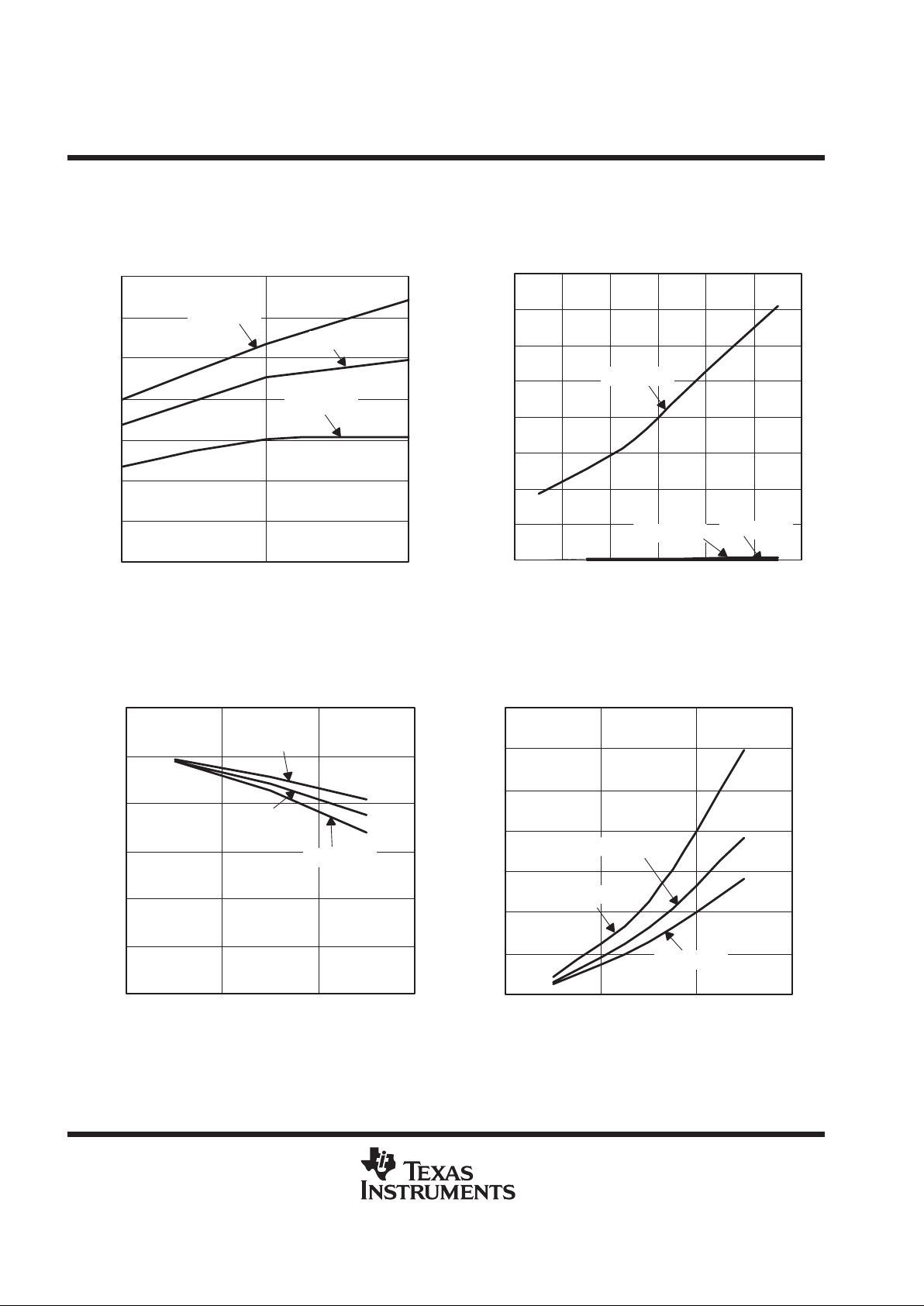
TYPICAL CHARACTERISTICS
Figure 1
600
650
700
750
800
850
900
950
4.5 7.0 25.0
VCC – Supply Voltage – V
TJ = 125°C
– Quiescent Current –
QUIESCENT CURRENT (BOTH CHANNELS ON)
vs
SUPPLY VOLTAGE
Aµ
I
(qon)
TJ = 25°C
TJ = –40°C
Figure 2
0.0
20.0
40.0
60.0
80.0
100.0
120.0
140.0
160.0
4.5 7.0 10.0 15.0 20.0 25.0
– Quiescent Current – nA
QUIESCENT CURRENT (BOTH CHANNEL STANDBY)
vs
SUPPLY VOLTAGE
I
(off)
TJ = 125°C
TJ = 25°C
TJ = –40°C
VCC – Supply Voltage – V
Figure 3
0
1
2
3
4
5
6
0.1 0.5 1
I
(src)
– Driver Source Current – A
– Driver Output Voltage – V
DRIVE OUTPUT VOLTAGE
vs
DRIVE CURRENT (SOURCE)
V
(src)
TJ = 125°C
TJ = 25°C
TJ = –40°C
Figure 4
0
0.5
1
1.5
2
2.5
3
3.5
0.1 0.5 1
I
(sink)
– Driver Sink Current – A
– Driver Output Voltage – V
DRIVE VOLTAGE
vs
DRIVE CURRENT (SINK)
V
(snk)
TJ = 125°C
TJ = 25°C
TJ = –40°C
 Loading...