

Page 1

SLUUBP7–December 2017
Using the TPS53681EVM-002, Dual Multiphase DC-DC
Step-Down Analog Controller with PMBus™ Interface
This User Guide describes the evaluation module (EVM) for the TPS53681 analog power controller, a
driverless D-CAP+™ multiphase buck controller, which manages several high current phases of the
CSD95490, a NexFet™ Smart Synchronous Buck Power Stage.
Contents
1 Description.................................................................................................................... 1
2 Typical Applications ......................................................................................................... 2
2.1 Features.............................................................................................................. 2
3 Electrical Performance Specifications..................................................................................... 3
4 Schematic..................................................................................................................... 4
5 Test Setup................................................................................................................... 12
5.1 Test and Configuration Software ................................................................................ 12
5.2 Test Equipment.................................................................................................... 12
5.3 Recommended Test Setup....................................................................................... 13
6 EVM Configuration Using the Fusion GUI .............................................................................. 14
6.1 Configuration Procedure ......................................................................................... 14
7 Test Procedure ............................................................................................................. 14
7.1 Line/Load Regulation and Efficiency Measurement Procedure............................................. 14
7.2 High Current Operation........................................................................................... 15
7.3 Multiphase/Multi-rail Configurations............................................................................. 16
7.4 On-Board Transient Load Operation............................................................................ 16
7.5 Efficiency ........................................................................................................... 17
7.6 Equipment Turn-on and Shutdown.............................................................................. 18
8 Performance Data and Typical Characteristic Curves................................................................. 19
9 EVM Assembly Drawing .................................................................................................. 24
10 Bill of Materials ............................................................................................................. 26
11 Fusion GUI .................................................................................................................. 30
1 Description
The TPS53681EVM implements a typical application for a low-voltage, high current dual output power
converter, operating from a nominal 12-V input rail to produce a 0.9-V output rail at up to 294 A of load
current and a 0.8-V rail at up to 47 A. The EVM includes test points for evaluating the performance of the
TPS53681 controller and CSD95490 power stages.
For ease of evaluation, the EVM requires only one (12-V) input supply and an output load to get started
with testing, however the user can opt to independently provide 5-V for greater control over the Power
Stage voltage. With the addition of the Fusion Digital Power™ Designer software, the EVM’s PMBus™
interface allows access to the controller NVM for evaluation of additional configuration, control and
monitoring possibilities. Refer to the TPS53681 datasheet (SLUSCT1) for complete information on
configuring multi-phase operation with this controller.
SLUUBP7–December 2017
Submit Documentation Feedback
Using the TPS53681EVM-002, Dual Multiphase DC-DC Step-Down Analog
Copyright © 2017, Texas Instruments Incorporated
Controller with PMBus™ Interface
1
Page 2

Typical Applications
2 Typical Applications
• High current ASIC and FPGA core power in the following equipment:
– Wired and Wireless Networking
– Enterprise Server and Storage Networks
– Test & Measurement
– Smart Grid Infrastructure
– Aerospace and Defense
– Merchant Power Supplies
2.1 Features
• Dual regulated high current outputs
• Programmable settings available through PMBus™ interface
– Output voltage trim
– Output voltage margin levels (High / Low) within a maximum range
– UVLO protection threshold
– Soft-start slew-rate
– Device enable and disable
– Overcurrent warning and fault limits
– SW frequency
– BOOT voltage
– Monitoring of input & output voltage, current, power, and power stage temperature
• Convenient test points for probing critical waveforms
www.ti.com
2
Using the TPS53681EVM-002, Dual Multiphase DC-DC Step-Down Analog
Controller with PMBus™ Interface
Copyright © 2017, Texas Instruments Incorporated
SLUUBP7–December 2017
Submit Documentation Feedback
Page 3
www.ti.com
3 Electrical Performance Specifications
Table 1. TPS53681EVM Electrical Performance Specifications
PARAMETER TEST CONDITIONS MIN TYP MAX UNITS
INPUT CHARACTERISTICS
V
IN
I
IN(max)
OUTPUT CHARACTERISTICS
V
OUT
I
OUT
V
RIPPLE
SYSTEMS CHARACTERISTICS
f
SW
T
A
Voltage range 10 12 14 V
Maximum input current
VIN= 12 V, I
47 A
VIN= 12 V, I
No load input current
A, Dynamic Phase Shedding
disabled
Output voltage
Output load current
Output voltage load regulation
Output voltage ripple
Output overcurrent protection
(OCP)
RAIL A 0.9 V
RAIL B 0.8 V
RAIL A (6-phase mode) 0 294 A
RAIL B (2-phase mode) 0 47 A
0 A ≤ I
0 A ≤ I
VIN= 12 V, I
VIN= 12 V, I
RAIL A 382.5 A
Rail A Switching frequency VIN= 12 V 500 kHz
Rail A Peak efficiency VIN= 12 V, I
Rail A Full-load efficiency VIN= 12 V, I
Rail B Switching frequency VIN= 12 V 500 kHz
Rail B Peak efficiency VIN= 12 V, I
Rail B Full-load efficiency VIN= 12 V, I
Operating temperature 25 ºC
Electrical Performance Specifications
= 294 A, I
OUTA
= 0 A, I
OUTA
≤ 294 A 0.15%
OUTA
≤ 47 A 0.15%
OUTB
= 150 A 4 mVpp
OUTA
= 45 A 5 mVpp
OUTB
= 90 A 93.0%
OUTA
= 294 A 87.5%
OUTA
= 25 A 91.8%
OUTB
= 47 A 90.6%
OUTB
OUTB
OUTB
=
= 0
30 A
330 mA
SLUUBP7–December 2017
Submit Documentation Feedback
Using the TPS53681EVM-002, Dual Multiphase DC-DC Step-Down Analog
Copyright © 2017, Texas Instruments Incorporated
Controller with PMBus™ Interface
3
Page 4
Schematic
www.ti.com
4
SLUUBP7–December 2017
Submit Documentation Feedback
Copyright © 2017, Texas Instruments Incorporated
Using the TPS53681EVM-002, Dual Multiphase DC-DC Step-Down Analog
Controller with PMBus™ Interface
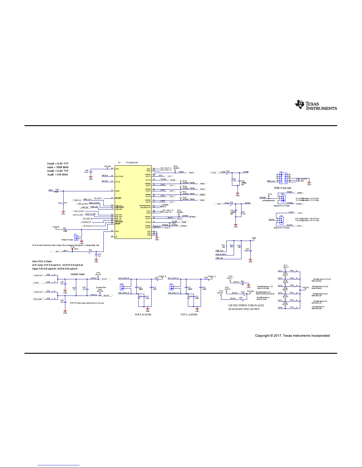
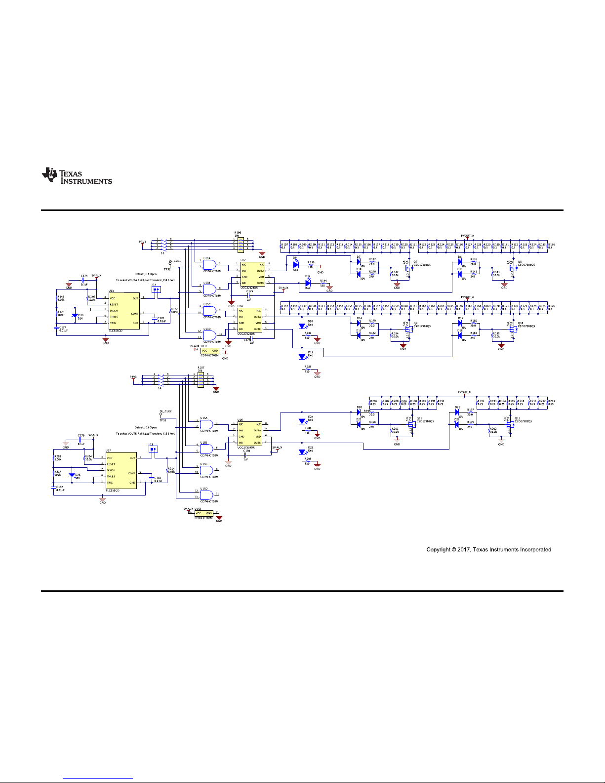
4 Schematic
Figure 1. TPS53681EVM - Controller Schematic
Page 5
www.ti.com
Schematic
5
SLUUBP7–December 2017
Submit Documentation Feedback
Copyright © 2017, Texas Instruments Incorporated
Using the TPS53681EVM-002, Dual Multiphase DC-DC Step-Down Analog
Controller with PMBus™ Interface
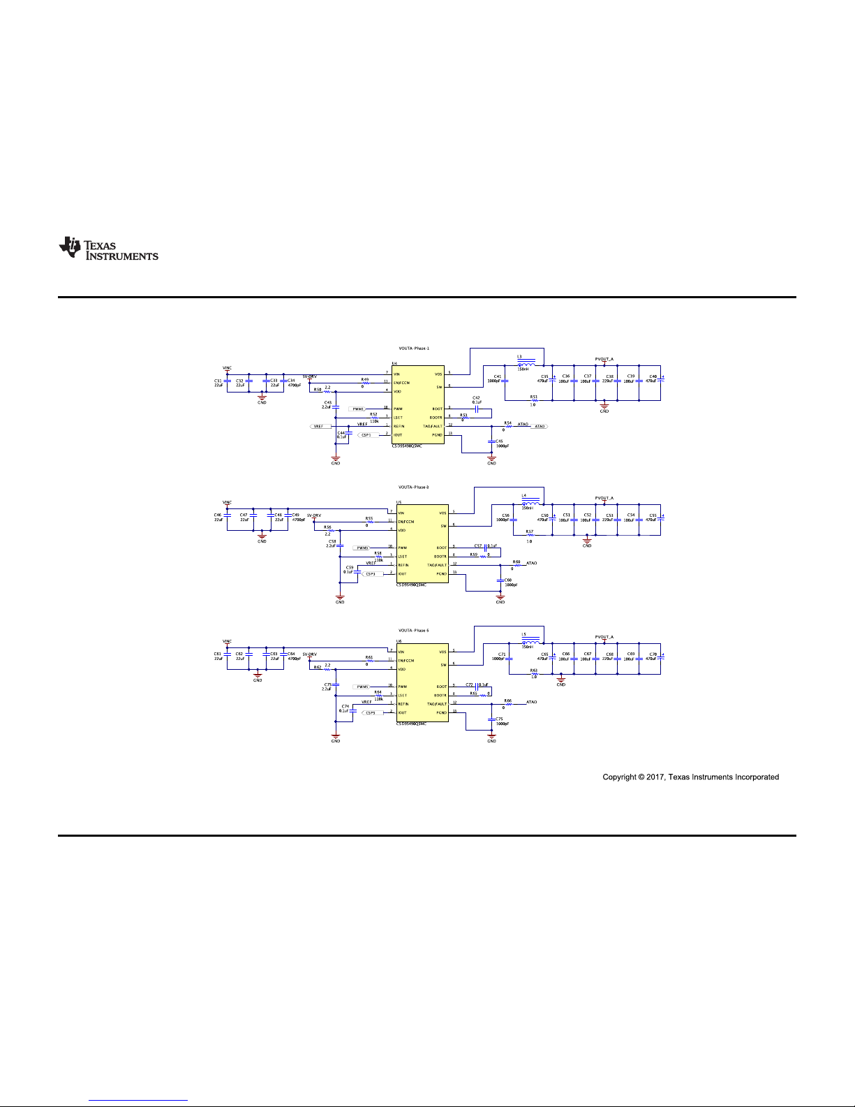
Figure 2. TPS53681EVM - Rail A Power Stages 1-3-5 Schematic
Page 6
Schematic
www.ti.com
6
SLUUBP7–December 2017
Submit Documentation Feedback
Copyright © 2017, Texas Instruments Incorporated
Using the TPS53681EVM-002, Dual Multiphase DC-DC Step-Down Analog
Controller with PMBus™ Interface
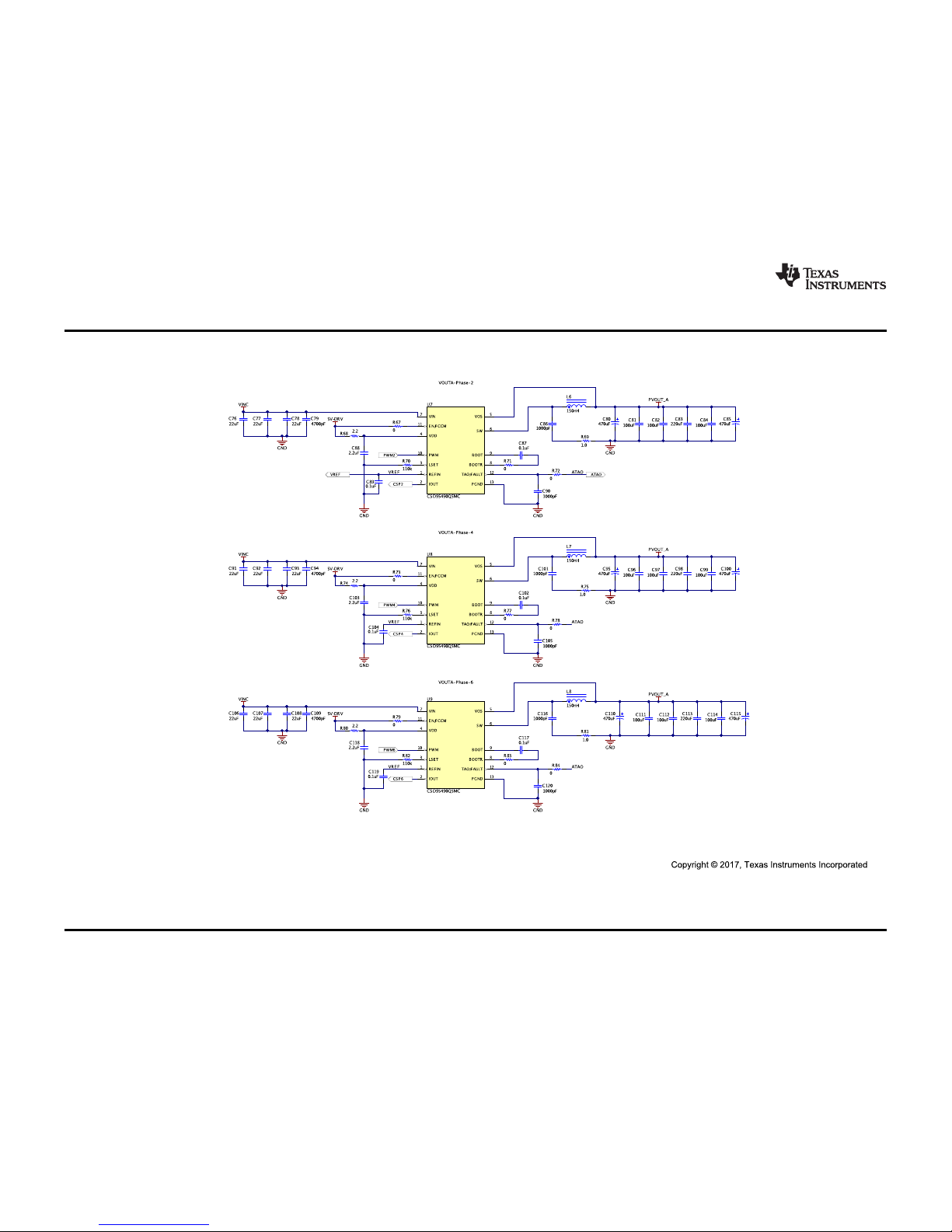
Figure 3. TPS53681EVM - Rail A Power Stages 2-4-6 Schematic
Page 7
www.ti.com
Schematic
7
SLUUBP7–December 2017
Submit Documentation Feedback
Copyright © 2017, Texas Instruments Incorporated
Using the TPS53681EVM-002, Dual Multiphase DC-DC Step-Down Analog
Controller with PMBus™ Interface
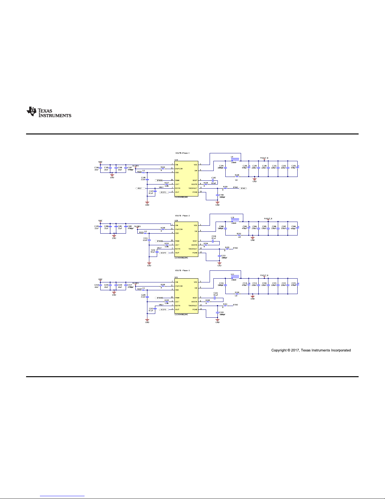
Figure 4. TPS53681EVM - Rail B Power Stages Schematic
Page 8
Schematic
www.ti.com
8
SLUUBP7–December 2017
Submit Documentation Feedback
Copyright © 2017, Texas Instruments Incorporated
Using the TPS53681EVM-002, Dual Multiphase DC-DC Step-Down Analog
Controller with PMBus™ Interface
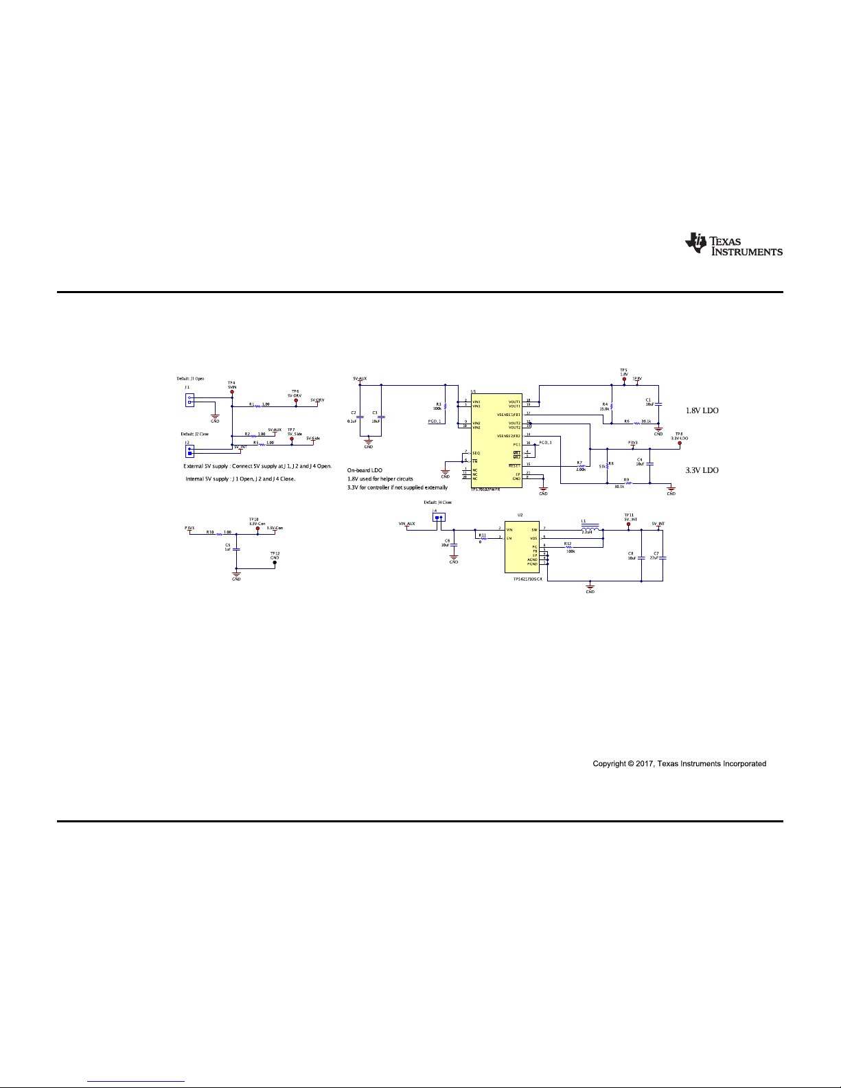
Figure 5. TPS53681EVM - AUX Voltages Schematic
Page 9
www.ti.com
Schematic
9
SLUUBP7–December 2017
Submit Documentation Feedback
Copyright © 2017, Texas Instruments Incorporated
Using the TPS53681EVM-002, Dual Multiphase DC-DC Step-Down Analog
Controller with PMBus™ Interface
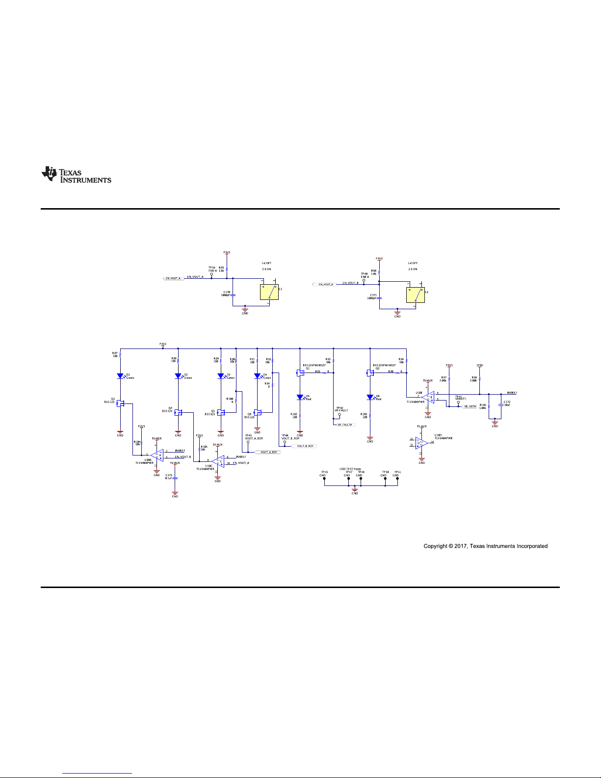
Figure 6. TPS53681EVM - Helper Circuits and Indicators Schematic
Page 10
Schematic
www.ti.com
10
SLUUBP7–December 2017
Submit Documentation Feedback
Copyright © 2017, Texas Instruments Incorporated
Using the TPS53681EVM-002, Dual Multiphase DC-DC Step-Down Analog
Controller with PMBus™ Interface
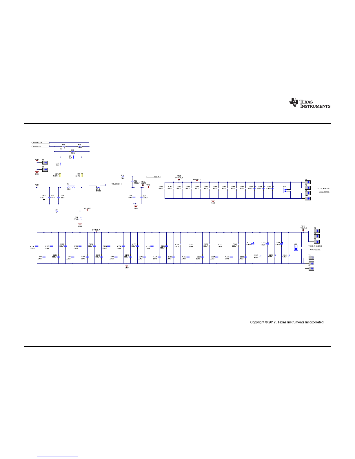
Figure 7. TPS53681EVM - Input and Output Filter Schematic
Page 11
www.ti.com
Schematic
11
SLUUBP7–December 2017
Submit Documentation Feedback
Copyright © 2017, Texas Instruments Incorporated
Using the TPS53681EVM-002, Dual Multiphase DC-DC Step-Down Analog
Controller with PMBus™ Interface
Figure 8. TPS53681EVM - On Board Transient Load Schematic
Page 12

Test Setup
5 Test Setup
5.1 Test and Configuration Software
The Texas Instruments Fusion Digital Power Designer software can expand the functionality of the EVM.
To download this software, visit the Fusion Digital Power Software page.
5.1.1 Description
The Fusion Digital Power Designer is a graphical user interface (GUI) used to configure, control and
monitor the TPS53681 controller on the EVM. The software uses the PMBus™ protocol to communicate
with the controller over a serial bus by way of the TI USB-to-GPIO Adapter.
5.1.2 TI Fusion Digital Power Designer Features
The software offers these features:
• Turn on or off the power supply output, either through the hardware control line or the PMBus™
Operation command.
• Monitor real-time data. Items such as input voltage, input current, output voltage, output current,
temperature, warnings and faults are continuously monitored and displayed by the GUI.
• Configure common operating characteristics such as output voltage trim and margin, VINUVLO, soft-
start slew rate, switching frequency, and warning and fault thresholds.
5.2 Test Equipment
www.ti.com
5.2.1 Voltage Sources
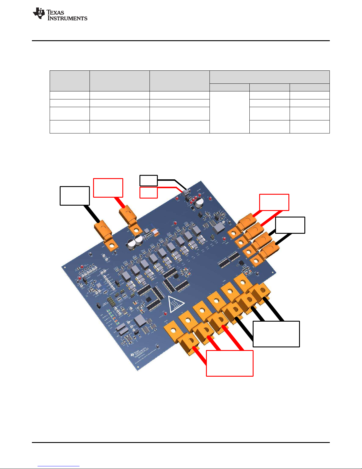
Only one DC input voltage sources is needed (VIN). The VIN input voltage source should be a 0 V to 14 V
variable DC source capable of supplying 40 Adc. Connect VIN to terminals J6 and J7 as shown in
Figure 9.
For greater control during testing, one can remove jumpers from J2 and J4 to bypass the onboard 5-V
power supply. This external supply should be limited to 1 Adc.
5.2.2 Multimeters
It is recommended to use two separate multimeters, one meter to measure VINand the other to measure
V
.
OUT
5.2.3 Output Load
An electronic load is recommended for the test setup shown in Figure 9. To observe the Rail A at full load
the electronic load should be capable of sinking 294 A at 0.9-V (Rail B, 47 A at 0.8-V).
5.2.4 Oscilloscope
Use an oscilloscope to measure output noise and ripple. Use a coaxial cable to measure output ripple
across the output ceramic capacitors.
5.2.5 Fan
During prolonged operation at high load (More than 100 A), it is necessary to provide forced air cooling
with a small fan aimed at the EVM. Maintain the temperature of the devices on the EVM under 115°C.
5.2.6 USB-to-GPIO Interface Adapter
A communications adapter is required between the EVM and the host computer. This EVM is designed to
use the Texas Instruments USB-to-GPIO adapter connected to J12. To purchase this adapter visit the TI
USB-to_GPIO tool page.
12
Using the TPS53681EVM-002, Dual Multiphase DC-DC Step-Down Analog
Controller with PMBus™ Interface
Copyright © 2017, Texas Instruments Incorporated
SLUUBP7–December 2017
Submit Documentation Feedback
Page 13
GND
12VIN
VOUTA+
VOUTB+
GND
GND
5VIN*
GND
*IF EXTERNAL
SOURCE IS USED
www.ti.com
5.2.7 Recommended Wire Gauge
VOLTAGE (V) CONNECT
12 VIN to J6, GND to J7 2 x AWG #8
5 (if J2 open) 5VIN to J1 2 x AWG #18 2 n/a
0.9
0.8
(1)
Total length of wire less than 4 feet (2 feet input or output, 2 feet return).
Load+ to T1, T2, and T3,
Load- to T4, T5, and T6
Load+ to T7 and T8,
Load- to T9 and T10
5.3 Recommended Test Setup
Figure 9 shows the recommended test setup, which includes VIN input voltage source(s) and output load.
Table 2. Recommended Wire Gauge
RECOMMENDED
WIRE SIZE
6 × AWG #4 n/a 2
4 × AWG #8 n/a 2
MAXIMUM TOTAL WIRE LENGTH
RETURN INPUT OUTPUT
2
Test Setup
(1)
(FEET)
2 n/a
Figure 9. TPS53681EVM Recommended Test Setup
SLUUBP7–December 2017
Submit Documentation Feedback
Using the TPS53681EVM-002, Dual Multiphase DC-DC Step-Down Analog
Copyright © 2017, Texas Instruments Incorporated
Controller with PMBus™ Interface
13
Page 14
EVM Configuration Using the Fusion GUI
6 EVM Configuration Using the Fusion GUI
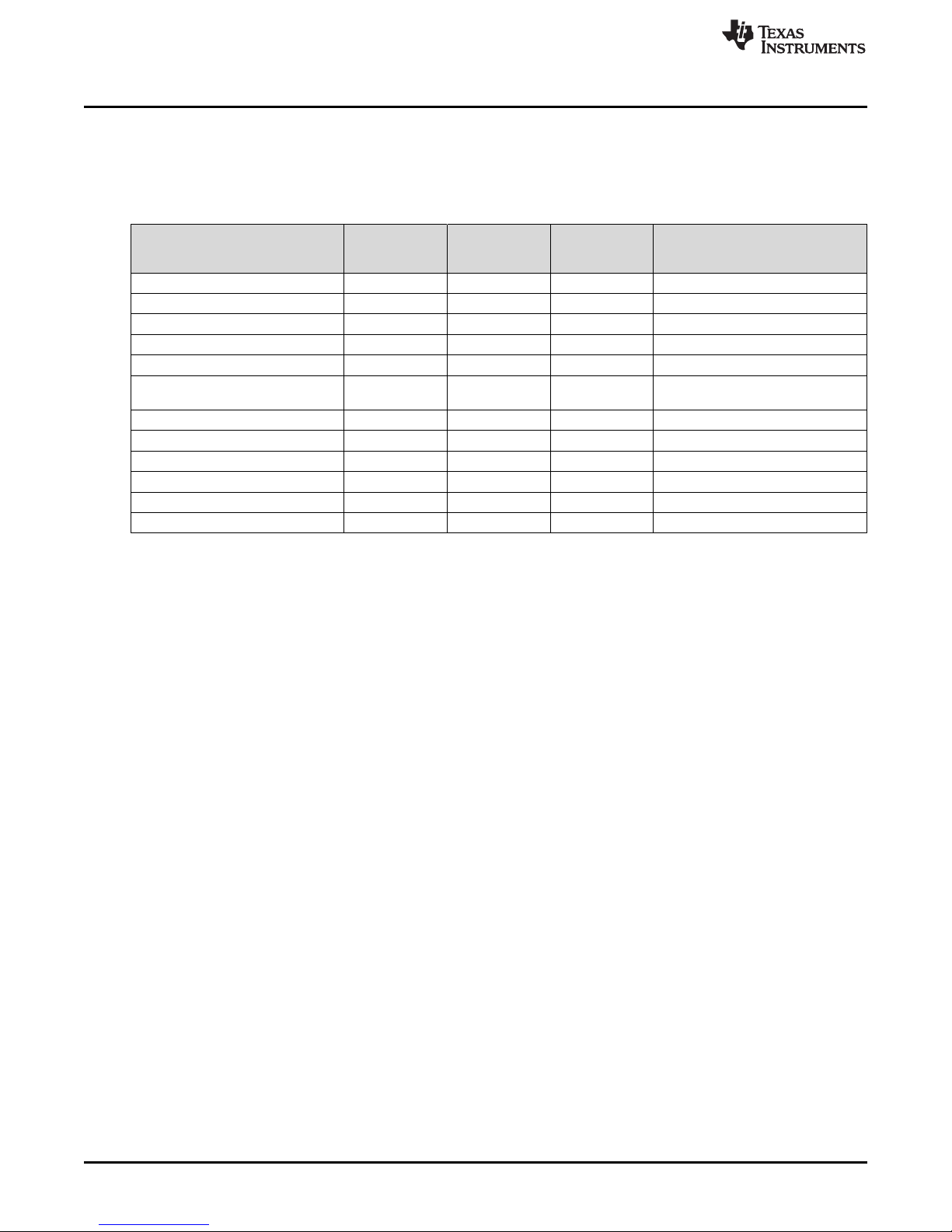
The controller on this EVM leaves the factory pre-configured. Table 3 lists some key factory configuration
parameters from the configuration file.
Table 3. Key Factory Configuration Parameters
www.ti.com
CMD NAME PMBus
VIN_ON 0x35 0xF029 10.25 V Input voltage turn on threshold
Rail A IOUT_OC_FAULT_LIMIT 0x46 0x017E 382.00 A Rail A OC fault level
Rail A IOUT_OC_WARN_LIMIT 0x4A 0x00FF 255.0 A Rail A OC warning level
Rail B IOUT_OC_FAULT_LIMIT 0x46 0x005A 135.00 A Rail B OC fault level
Rail B IOUT_OC_WARN_LIMIT 0x4A 0x0087 90.0 A Rail BOC warning level
ON_OFF_CONFIG 0x02 0x17 Control Pin only Power is converted when the control
OT_FAULT_LIMIT 0x4F 0x0073 115 °C OT fault level
OT_WARN_LIMIT 0x51 0x0069 105 °C OT warning level
Rail A Max Num Phases 0xE4 0x05 6 Phase Rail number of phases
FSW 0x33 0x01F4 500kHz Switching frequency
Rail A VBOOT 0xDB 0x83 0.900V Rail A VBOOT voltage
Rail B VBOOT 0xDB 0x6F 0.800V Rail B VBOOT voltage
To configure the EVM with other than the factory settings shown in Table 3, use the TI Fusion Digital
Power Designer software for reconfiguration. Be sure to apply input voltage to the EVM prior to launching
the software. This sequence ensures that the controller and GUI recognize each other.
6.1 Configuration Procedure
1. Connect USB-to-GPIO adaptor to J12.
2. Apply the input power source VIN to the EVM. Refer to Figure 9.
3. Ensure that the controller is receiving 3.3-V (either through the onboard LDOs or an external supply)
4. Launch the Fusion GUI software.
5. Configure the EVM operating parameters as desired.
COMMAND
CODE
HEX VALUE PHYSICAL
SETTING
COMMENTS
pin is active
7 Test Procedure
7.1 Line/Load Regulation and Efficiency Measurement Procedure
1. Set up EVM as shown in Figure 9.
2. Ensure the electronic load is set to draw 0 Adc.
3. Check to see if jumpers are in desired configuration (Refer to Table 4)
4. Increase VIN from 0-V to 12-V.
5. Change the relevant switch to ON position (S1 for Rail A, S2 for Rail B).
6. Turn on the external fan if necessary (When driving a load above 50A).
7. Vary the load from 0 Adc to 294 Adc for Rail A (0 Adc to 47 Adc for Rail B) Ensure V
regulation as defined in Table 1.
8. Vary VIN from 10-V to 14-V. Ensure V
9. Decrease the load to 0 A.
10. Change relevant switch to OFF position (S1 for Rail A, S2 for Rail B).
11. Decrease VIN to 0 V.
12. Shut down the external fan if in use.
14
Using the TPS53681EVM-002, Dual Multiphase DC-DC Step-Down Analog
Controller with PMBus™ Interface
remains in regulation as defined in Table 1.
OUT
Copyright © 2017, Texas Instruments Incorporated
remains in
OUT
SLUUBP7–December 2017
Submit Documentation Feedback
Page 15

www.ti.com
Table 4. Connector Functions
CONNECTOR DESCRIPTION
J1 5VIN External Supply Input
J2 5VIN Supply Selector (Closed by Default to Activate Internal 5VIN Supply)
J4 Internal 5VIN Supply Input (Closed by Default to Activate Internal 5VIN Supply)
J6 VIN+ Connector
J7 VIN- Connector
J8 PWM Configuration Connector (Default Pin 2-3 Shorted for 6+2 Configuration)
J9 Reset (Open by Default)
J10 CSP Configuration Connector (Default Pin 2-3 Shorted for 6+2 Configuration)
J11 V
J12 PMBUS Connector
J13 V
J14 V
J15 V
J16 V
J17 V
T1,T2.T3 V
T4,T5,T6 V
T7, T8 V
T9, T10 V
Sense (Leave Open!)
OUTA
Sense (Leave Open!)
OUTB
Onboard Transient Load Signal Generator Selector (Open by default)
OUTA
Onboard Transient Load Signal Generator Selector (Open by default)
OUTB
Output Measurement Point (Leave Open!)
OUTA
Output Measurement Point (Leave Open!)
OUTB
OUTA + Connectors
OUTA - Connectors
OUTB + Connectors
- Connectors
OUTB
Test Procedure
7.2 High Current Operation
When operating at with loads larger than 100A, one must provide ample cooling to the board, particularly
towards the CSD95490 power stages. Provide at least 100CFM of airflow over the power stages to keep
the board within its thermal limits. By default, this board will stop delivering a switching signal to power
stages when they reach a temperature above 115°C.
Similarly, when using the onboard transient load, one mustn't use a duty cycle wider than 20%, otherwise
the load resistors will overheat.
A VIN=12 V, V
OUT
= 0.9 V, I
OUT
=294A
Figure 10. Thermal Picture of TPS53681 EVM. Rail A with Full Load Cooled at 100CFM
SLUUBP7–December 2017
Submit Documentation Feedback
Using the TPS53681EVM-002, Dual Multiphase DC-DC Step-Down Analog
Copyright © 2017, Texas Instruments Incorporated
Controller with PMBus™ Interface
15
Page 16

Test Procedure
7.3 Multiphase/Multi-rail Configurations
This board is set up in a 6+2 configuration by default (Rail A with six phases, Rail B with two). If one
wishes to change to other configurations consult Table 5. For more information on setting the number of
phases on Rail B, please refer to SLUSCT1, section 7.3.1.5.
Table 5. Phase-Rail Configurations
www.ti.com
NUMBER OF PHASES ACTIVE ON
RAIL A
1 0 Short Pin 2-3 Short Pin 2-3 R29=0Ω, R35=10kΩ
2 0 Short Pin 2-3 Short Pin 2-3 R30=0Ω, R35=10kΩ
3 0 Short Pin 2-3 Short Pin 2-3 R31=0Ω, R35=10kΩ
4 0 Short Pin 2-3 Short Pin 2-3 R32=0Ω, R35=10kΩ
5 0 Short Pin 2-3 Short Pin 2-3 R33=0Ω, R35=10kΩ
6 0 Short Pin 2-3 Short Pin 2-3 R35=10kΩ
1 1 Short Pin 2-3 Short Pin 2-3 R29=0Ω, R38=0Ω
2 1 Short Pin 2-3 Short Pin 2-3 R30=0Ω, R38=0Ω
3 1 Short Pin 2-3 Short Pin 2-3 R31=0Ω, R38=0Ω
4 1 Short Pin 2-3 Short Pin 2-3 R32=0Ω, R38=0Ω
5 1 Short Pin 2-3 Short Pin 2-3 R33=0Ω, R38=0Ω
6 1 Short Pin 2-3 Short Pin 2-3 R38=0Ω, R41=0Ω
1 2 Short Pin 2-3 Short Pin 2-3 R29=0Ω, R41=0Ω
2 2 Short Pin 2-3 Short Pin 2-3 R30=0Ω, R41=0Ω
3 2 Short Pin 2-3 Short Pin 2-3 R31=0Ω, R41=0Ω
4 2 Short Pin 2-3 Short Pin 2-3 R32=0Ω, R41=0Ω
5 2 Short Pin 2-3 Short Pin 2-3 R33=0Ω, R41=0Ω
6 2 Short Pin 2-3 Short Pin 2-3 1 3 Short Pin 1-2 Short Pin 1-2 R29=0Ω
2 3 Short Pin 1-2 Short Pin 1-2 R30=0Ω
3 3 Short Pin 1-2 Short Pin 1-2 R31=0Ω
4 3 Short Pin 1-2 Short Pin 1-2 R32=0Ω
5 3 Short Pin 1-2 Short Pin 1-2 -
NUMBER OF
PHASES
ACTIVE ON
RAIL B
STATE OF
JUMPER J8
STATE OF
JUMPER J10
CSP RESISTORS TO POPULATE
7.4 On-Board Transient Load Operation
1. Set up EVM as shown in Figure 9.
2. Place Jumper J14 (J15 for Rail B) in order to provide drive signal from onboard 555 timer (~1.2 kHz,
8% Duty cycle) or inject drive signal in TP52 (T53 for Rail B) from signal generator. Take care not to
exceed 20% duty cycle if using external signal generator.
3. Turn ON one or more "banks" of load resistors with S3 (S4 for Rail B). At the default output voltages,
each "Bank" on Rail A adds 37.5A to the transient load. Likewise each "bank" on Rail B adds 23 A.
4. To best observe transient effects, measure voltage across J16 (J17 for Rail B)
5. Turn OFF S3 (or S4) when finished observing transient effects.
6. Disconnect J14 (or J15) or turn off signal generator output.
16
Using the TPS53681EVM-002, Dual Multiphase DC-DC Step-Down Analog
Controller with PMBus™ Interface
Copyright © 2017, Texas Instruments Incorporated
SLUUBP7–December 2017
Submit Documentation Feedback
Page 17

VIN
GND
VOUT
www.ti.com
7.5 Efficiency
In order to observe the efficiency of the power train on the EVM, it is important to measure the input and
output voltages at specific locations on the input and output capacitors nearest the power-stages. This is
necessary to prevent the inclusion of losses that are not specifically related to the power train itself, such
as losses incurred by the voltage drop in the copper traces or in the input and output connectors. It is
recommended that voltage measurements are measured with reference to the same ground.
Input current can be measured at any point in the input wires, and output current can be measured
anywhere in the output wires of the output being measured.
Figure 11 shows the measurement points that were used for the input voltage and output voltage. Using
these measurement points results in an efficiency derivation which does not include losses due to the
connectors and PCB traces.
Also make sure to provide the 5-V gate drive voltage separately through J1 (leaving J2 and J4 open) if
one wishes to observe efficiency independent of gate-drive and controller losses. R1, R2, R5, and R10 are
installed as shunts to help the user measure current in the auxiliary and drive circuits.
Test Procedure
Figure 11. Test Setup for Efficiency Measurement
SLUUBP7–December 2017
Submit Documentation Feedback
Using the TPS53681EVM-002, Dual Multiphase DC-DC Step-Down Analog
Copyright © 2017, Texas Instruments Incorporated
Controller with PMBus™ Interface
17
Page 18

Test Procedure
7.6 Equipment Turn-on and Shutdown
7.6.1 Turn-on Sequence
1. If using an external 5 V source (J2 and J4 left open), turn on input power supply and increase 5VIN to
5 V
2. Turn on input power supply VIN and increase VIN above 10.5 V.
3. Switch S1 (S2 for Rail B) to ‘ON’ position.
4. Adjust load current as desired.
5. Turn on external fan if necessary.
7.6.2 Shutdown Sequence
1. Reduce the load current to 0 A.
2. Switch S1 (or S2) to ‘OFF’ position.
3. Reduce input voltage to 0 V and shut down input power supply VIN, then 5VIN if used.
4. Shut down the external fan if in use.
www.ti.com
18
Using the TPS53681EVM-002, Dual Multiphase DC-DC Step-Down Analog
Controller with PMBus™ Interface
Copyright © 2017, Texas Instruments Incorporated
SLUUBP7–December 2017
Submit Documentation Feedback
Page 19

IOUT (A)
VOUT (V)
0 50 100 150 200 250 300
0.8985
0.8987
0.8989
0.8991
0.8993
0.8995
0.8997
0.8999
0.9001
TPS5
IOUT (A)
VOUT (A)
0 10 20 30 40 50
0.798
0.7983
0.7986
0.7989
0.7992
0.7995
0.7998
0.8001
TPS5
IOUT (A)
Efficiency (%)
0 10 20 30 40 50
0.7
0.75
0.8
0.85
0.9
0.95
1
TPS5
IOUT (A)
Efficiency (%)
0 50 100 150 200 250 300
70%
75%
80%
85%
90%
95%
100%
TPS5TPS5
www.ti.com
Performance Data and Typical Characteristic Curves
8 Performance Data and Typical Characteristic Curves
Figure 12 through Figure 17 show performance curves for the TPS53681EVM.
The waveforms and bode plots shown below were made after making the following changes from the
default settings using our Fusion Digital Power Software .
Rail A Setting Change
• [Figure 48,Transients] AC_LL: 0.2500mΩ
Rail B Setting Changes
• [Figure 48,Transients] AC_GAIN: 2.00 *x
• [Figure 48,Transients] AC_LL: 0.2500mΩ
• [Figure 48,Transients] INT_Time: 02µs
• [Figure 48,Transients] INTGAIN: 2.00*x
• [Figure 46, Static] IOUT_MAX: 47A
These changes can either be done manually, as described in the Section 11 section or one can download
a complete, reconfigured .xml configuration file from the TPS53681EVM webpage, and upload it to the
device as shown here .
V
= 0.9 V, VIN=12 V
OUT
Figure 12. VOUT A Power Stage Efficiency Figure 13. VOUT B Power Stage Efficiency
VOUT = 0.9 V, VIN =12 V VOUT = 0.8 V, VIN =12 V
Figure 14. VOUT A Load Regulation Figure 15. VOUT B Load Regulation
SLUUBP7–December 2017
Submit Documentation Feedback
V
= 0.8 V, VIN=12 V
OUT
Using the TPS53681EVM-002, Dual Multiphase DC-DC Step-Down Analog
Copyright © 2017, Texas Instruments Incorporated
Controller with PMBus™ Interface
19
Page 20

Frequency (Hz)
Gain (dB)
Phase (q)
1000 2000 5000 10000 100000 1000000
-100 -200
-80 -160
-60 -120
-40 -80
-20 -40
0 0
20 40
40 80
60 120
80 160
100 200
Gain
Phase
Frequency (Hz)
Gain (dB)
Phase (q)
1000 2000 5000 10000 100000 1000000
-100 -200
-80 -160
-60 -120
-40 -80
-20 -40
0 0
20 40
40 80
60 120
80 160
100 200
Gain
Phase
Performance Data and Typical Characteristic Curves
VIN = 12 V VOUT = 0.9 V IOUT = 50 A VIN = 12 V VOUT = 0.8 V IOUT = 45 A
Figure 16. VOUT A Bode Plot Figure 17. VOUT B Bode Plot
www.ti.com
20
Using the TPS53681EVM-002, Dual Multiphase DC-DC Step-Down Analog
Controller with PMBus™ Interface
Copyright © 2017, Texas Instruments Incorporated
SLUUBP7–December 2017
Submit Documentation Feedback
Page 21

www.ti.com
Figure 19 through Figure 23 show the waveforms for the TPS53681EVM.
Performance Data and Typical Characteristic Curves
VIN = 12 V, VOUT = 0.9 V
Figure 18. VOUT A Transient Response (Load Step 0 A
to 150 A, 500 A/µs Slew Rate)
VIN = 12 V, VOUT = 0.9 V
Figure 20. VOUT A Transient Response (Load Step 0 A
to 150 A to 0 A, 500 A/µs Slew Rate)
VIN = 12 V, VOUT = 0.9 V
Figure 19. VOUT A Transient Response (Load Step 150
A to 0 A, 500 A/µs Slew Rate)
VIN = 12 V, VOUT = 0.9 V, IOUT = 150 A
Figure 21. VOUT A Output Ripple
SLUUBP7–December 2017
Submit Documentation Feedback
Using the TPS53681EVM-002, Dual Multiphase DC-DC Step-Down Analog
Copyright © 2017, Texas Instruments Incorporated
Controller with PMBus™ Interface
21
Page 22

Performance Data and Typical Characteristic Curves
www.ti.com
VIN = 12 V, VOUT= 0.9 V, IOUT = 50 A
Figure 22. VOUT A Enable Startup Figure 23. VOUT A Enable Shutdown
VIN = 12 V, VOUT = 0.8 V
Figure 24. VOUT B Transient Response (Load Step 0 A
to 45 A, 500 A/µs Slew Rate)
VIN = 12 V, VOUT = 0.9 V, IOUT = 50 A
VIN = 12 V, VOUT = 0.8 V
Figure 25. VOUT B Transient Response (Load Step 45 A
to 0 A, 500 A/µs Slew Rate)
22
Using the TPS53681EVM-002, Dual Multiphase DC-DC Step-Down Analog
Controller with PMBus™ Interface
Copyright © 2017, Texas Instruments Incorporated
SLUUBP7–December 2017
Submit Documentation Feedback
Page 23

www.ti.com
Performance Data and Typical Characteristic Curves
VIN = 12 V, VOUT = 0.8 V
Figure 26. VOUT B Transient Response (Load Step 0 A
VIN = 12 V, VOUT = 0.8 V, IOUT = 45 A
Figure 27. VOUT B Output Ripple
to 45 A to 0 A, 500 A/µs Slew Rate)
VIN = 12 V, VOUT = 0.8 V, IOUT = 0 A VIN = 12 V, VOUT = 0.8 V, IOUT = 6 A
Figure 28. VOUT B Enable Startup Figure 29. VOUT B Enable Shutdown
SLUUBP7–December 2017
Submit Documentation Feedback
Using the TPS53681EVM-002, Dual Multiphase DC-DC Step-Down Analog
Copyright © 2017, Texas Instruments Incorporated
Controller with PMBus™ Interface
23
Page 24

EVM Assembly Drawing
9 EVM Assembly Drawing
Figure 30. Top Layer Assembly Drawing (Top View) Figure 31. Bottom Layer Assembly Drawing (Bottom View)
www.ti.com
Figure 32. Top Copper (Top View) Figure 33. Internal Layer 1 (Top View)
Figure 34. Internal Layer 2 (Top View) Figure 35. Internal Layer 3 (Top View)
24
Using the TPS53681EVM-002, Dual Multiphase DC-DC Step-Down Analog
Controller with PMBus™ Interface
Copyright © 2017, Texas Instruments Incorporated
SLUUBP7–December 2017
Submit Documentation Feedback
Page 25

www.ti.com
EVM Assembly Drawing
Figure 36. Internal Layer 4 (Top View) Figure 37. Internal Layer 5 (Top View)
Figure 38. Internal Layer 6 (Top View) Figure 39. Internal Layer 7 (Top View)
Figure 40. Internal Layer 8 (Top View) Figure 41. Bottom Copper (Top View)
SLUUBP7–December 2017
Submit Documentation Feedback
Using the TPS53681EVM-002, Dual Multiphase DC-DC Step-Down Analog
Copyright © 2017, Texas Instruments Incorporated
Controller with PMBus™ Interface
25
Page 26

Bill of Materials
10 Bill of Materials
www.ti.com
Table 6. Bill of Materials
Qu
ant
ity
5 C1, C3, C4, C8, C172
3 C2, C29, C173
6 C5, C9, C18, C26, C28, C30
1 C6
1 C7
1 C10
2 C11, C12
3 C13, C14, C15
1 C16
2 C19, C20
2 C21, C24
C31, C32, C33, C46, C47, C48, C61,
C62, C63, C76, C77, C78, C91, C92,
27
C93, C106, C107, C108, C184, C185,
C186, C199, C200, C201, C214, C215,
C34, C49, C64, C79, C94, C109, C187,
9
C35, C40, C50, C55, C65, C70, C80,
C85, C95, C100, C110, C115, C121,
27
C122, C123, C139, C140, C141, C157,
C158, C159, C188, C193, C203, C208,
C38, C53, C68, C83, C98, C113, C124,
C125, C127, C129, C130, C132, C134,
24
C135, C137, C142, C144, C145, C147,
C149, C150, C152, C154, C155
C42, C57, C72, C87, C102, C117, C195,
9
C43, C58, C73, C88, C103, C118, C196,
9
C126, C128, C131, C133, C136, C138,
C143, C146, C148, C151, C153, C156,
22
C160, C161, C162, C163, C164, C165,
2 C170, C171
2 C174, C179
3 C175, C178, C180
2 C176, C181
REF DES Description Part Number
C216
C202, C217
C218, C223
C210, C225
C211, C226
C166, C167, C168, C169
CAP, CERM, 10 uF, 25 V, +/- 10%, X5R,
0805
CAP, CERM, 0.1 uF, 50 V, +/- 10%,
X7R, 0603
CAP, CERM, 1 uF, 16 V, +/- 10%, X7R,
0603
CAP, CERM, 10 uF, 25 V, +/- 20%, X5R,
0603
CAP, CERM, 22 uF, 6.3 V, +/- 20%,
X5R, 0805
CAP, CERM, 0.082 uF, 16 V, +/- 10%,
X7R, 0603
CAP, CERM, 22 uF, 16 V, +/- 10%, X5R,
1206
CAP, Polymer Hybrid, 270 uF, 35 V, +/20%, 20 ohm, 10x10 SMD
CAP, CERM, 4.7 uF, 10 V, +/- 10%,
X5R, 0603
CAP, CERM, 1000 pF, 50 V, +/- 5%,
X7R, 0603
CAP, CERM, 100 pF, 25 V, +/- 5%,
C0G/NP0, 0402
CAP, CERM, 22 uF, 16 V, +/- 20%, X5R,
0805
CAP, CERM, 4700 pF, 50 V, +/- 10%,
X7R, 0402
CAP, Aluminum Polymer, 470 uF, 2.5 V,
+/- 20%, 0.003 ohm,
SMD_7.3x1.9x4.3mm SMD
CAP, CERM, 220 uF, 4 V, +/- 20%, X5R,
1206_190
CAP, CERM, 0.1 uF, 50 V, +/- 10%,
X7R, 0402
CAP, CERM, 2.2 uF, 10 V, +/- 10%,
X5R, 0402
CAP, CERM, 100 uF, 4 V, +/- 20%, X5R,
1206
CAP, CERM, 1000 pF, 100 V, +/- 10%,
X7R, 0603
CAP, CERM, 0.1 uF, 25 V, +/- 10%,
X7R, 0805
CAP, CERM, 1 uF, 16 V, +/- 10%, X5R,
0603
CAP, CERM, 0.01 uF, 100 V, +/- 5%,
X7R, 0805
Manufactur
er
C2012X5R1E106K125A
B
06035C104KAT2A AVX
C1608X7R1C105K080A
C
C1608X5R1E106M080A
C
C2012X5R0J226M085A
B
0603YC823KAT2A AVX
GRM31CR61C226KE15
L
EEHZA1V271P Panasonic
C0603C475K8PACTU Kemet
C0603C102J5RACTU Kemet
C0402C101J3GACTU Kemet
C2012X5R1C226M125A
C
GRM155R71H472KA01
D
EEF-GX0E471R Panasonic
GRM31CR60G227ME11
L
C1005X7R1H104K050B
B
C1005X5R1A225K050B
C
GRM31CR60G107ME39
L
C1608X7R2A102K080A
A
08053C104KAT2A AVX
C0603C105K4PACTU Kemet
08051C103JAT2A AVX
TDK
TDK
TDK
TDK
MuRata
TDK
MuRata
MuRata
TDK
TDK
MuRata
TDK
26
Using the TPS53681EVM-002, Dual Multiphase DC-DC Step-Down Analog
Controller with PMBus™ Interface
SLUUBP7–December 2017
Submit Documentation Feedback
Copyright © 2017, Texas Instruments Incorporated
Page 27

www.ti.com
Bill of Materials
Table 6. Bill of Materials (continued)
Qu
ant
ity
2 C177, C182
4 D1, D2, D3, D4 LED, Green, SMD LTST-C170KGKT Lite-On
8 D5, D6, D9, D12, D16, D19, D24, D25 LED, Red, SMD LTST-C170KRKT Lite-On
D7, D8, D10, D11, D14, D15, D17, D18,
12
2 D13, D28 Diode, Schottky, 30 V, 0.2 A, SOT-23 BAT54-7-F Diodes Inc.
4 H1, H2, H3, H4 Bumpon, Hemisphere, 0.44 X 0.20, Clear SJ-5303 (CLEAR) 3M
H5, H6, H7, H8, H9, H10, H11, H12,
12
H17, H18, H19, H20, H21, H22, H23,
12
H29, H30, H31, H32, H33, H34, H35,
12
1 J1 Terminal Block, 3.5 mm, 2x1, Tin, TH 39357-0002 Molex
9 J2, J4, J9, J11, J13, J14, J15, J16, J17 Header, 100mil, 2x1, Gold, TH TSW-102-07-G-S Samtec
6 J6, J7, T7, T8, T9, T10 Terminal 90A Lug CB70-14-CY Panduit
2 J8, J10 Header, 100mil, 3x1, Gold, TH TSW-103-07-G-S Samtec
1 J12 Header, 100mil, 5x2, Gold, TH TSW-105-07-G-D Samtec
1 L1
1 L2 Inductor, 55 nH, 30 A, 0.0002 ohm, SMD HCB65-550X
9 L3, L4, L5, L6, L7, L8, L9, L10, L11
2 Q1, Q2
4 Q3, Q4, Q5, Q6 MOSFET, N-CH, 100 V, 0.17 A, SOT-23 BSS123
6 Q7, Q8, Q9, Q10, Q11, Q12
4 R1, R2, R5, R10 RES, 1.00, 1%, 0.1 W, 0603 RC0603FR-071RL
4 R3, R12, R178, R217 RES, 100 k, 1%, 0.1 W, 0603 CRCW0603100KFKEA Vishay-Dale
1 R4 RES, 15.0 k, 1%, 0.1 W, 0603 CRCW060315K0FKEA Vishay-Dale
2 R6, R9 RES, 30.1 k, 1%, 0.1 W, 0603 CRCW060330K1FKEA Vishay-Dale
3 R7, R97, R98 RES, 2.00 k, 1%, 0.1 W, 0603 CRCW06032K00FKEA Vishay-Dale
1 R8 RES, 51 k, 5%, 0.1 W, 0603 CRCW060351K0JNEA Vishay-Dale
R11, R23, R24, R25, R34, R37, R39,
14
R40, R46, R48, R95, R96, R99, R100
3 R13, R22, R101 RES, 1.00 k, 1%, 0.1 W, 0603 CRCW06031K00FKEA Vishay-Dale
1 R14 RES, 6.04 k, 1%, 0.1 W, 0603 CRCW06036K04FKEA Vishay-Dale
1 R15 RES, 499, 1%, 0.1 W, 0603 CRCW0603499RFKEA Vishay-Dale
1 R16 RES, 10.0, 1%, 0.063 W, 0402 CRCW040210R0FKED Vishay-Dale
1 R17 RES, 1.0, 5%, 1 W, 2010
REF DES Description Part Number
CAP, CERM, 0.01 uF, 50 V, +/- 5%,
X7R, 0805
D20, D21, D22, D23
H13, H14, H15, H16
H24, H25, H26, H27, H28
H36, H37, H38, H39, H40
Diode, Schottky, 30 V, 0.5 A, SOD-123 MBR0530T1G
Machine Screw Pan Slotted 10-32 PMS 102 0050 SL
Machine Screw Nut, Hex, 3/8', Stn,
Steel, 10-32
Washer, Split Lock, #10 1477 Keystone
Inductor, Shielded, Composite, 2.2 uH,
1.3 A, 0.16 ohm, SMD
Inductor, 150 nH, 68 A, 0.0002035 ohm,
SMD
MOSFET, P-CH, -20 V, -0.39 A, SOT323
MOSFET, N-CH, 30 V, 100 A,
DQH0008A (VSON-CLIP-8)
RES, 0, 5%, 0.1 W, 0603 CRCW06030000Z0EA Vishay-Dale
08055C103JAT2A AVX
HNSS 102
XPL2010-222MLB Coilcraft
PA4390.151HLT
BSS223PWH6327
CSD17303Q5
CRCW20101R00JNEFH
P
Manufactur
er
ON
Semiconduct
or
B&F
Fastener
Supply
B&F
Fastener
Supply
Delta
Electronics
Inc.
Pulse
Engineering
Infineon
Technologie
s
Fairchild
Semiconduct
or
Texas
Instruments
Yageo
America
Vishay-Dale
SLUUBP7–December 2017
Submit Documentation Feedback
Using the TPS53681EVM-002, Dual Multiphase DC-DC Step-Down Analog
Copyright © 2017, Texas Instruments Incorporated
Controller with PMBus™ Interface
27
Page 28

Bill of Materials
Qu
ant
ity
1 R18 RES, 475 k, 1%, 0.1 W, 0603 CRCW0603475KFKEA Vishay-Dale
1 R19 RES, 154 k, 1%, 0.1 W, 0603 CRCW0603154KFKEA Vishay-Dale
9
27
R78, R79, R83, R84, R224, R228, R229,
9
9
2 R85, R86 RES, 1.0 k, 5%, 0.1 W, 0603 CRCW06031K00JNEA Vishay-Dale
6 R87, R88, R89, R91, R102, R103 RES, 180, 5%, 0.1 W, 0603 CRCW0603180RJNEA Vishay-Dale
2 R106, R187 RES, 10 k, 5%, 0.0625 W, 3.2x1.6mm TC164-JR-0710KL
60
6 R137, R138, R179, R180, R196, R197 RES, 20.0, 1%, 0.1 W, 0603 CRCW060320R0FKEA Vishay-Dale
6 R139, R144, R181, R186, R200, R205 RES, 330, 5%, 0.125 W, 0805 CRCW0805330RJNEA Vishay-Dale
6 R140, R141, R182, R183, R198, R199 RES, 249, 1%, 0.1 W, 0603 CRCW0603249RFKEA Vishay-Dale
8
4 R145, R177, R203, R214 RES, 8.06 k, 1%, 0.1 W, 0603 CRCW06038K06FKEA Vishay-Dale
16
1 RT1 Thermistor NTC, 1.0k ohm, 5%, 0603 NCP18XQ102J03RB MuRata
2 S1, S2 Switch, SPDT, Slide, On-On, 2 Pos, TH EG1218 E-Switch
2 S3, S4 DIP Switch, SPST 4Pos, Slide, TH 78B04ST Grayhill
7
1 SR_1 RES, 0.0005, 1%, 3 W, 4026 WSL4026L5000FEB Vishay-Dale
6 T1, T2, T3, T4, T5, T6 Terminal 125A Lug CB125-14-QY Panduit
11
7
27
Table 6. Bill of Materials (continued)
REF DES Description Part Number
R42, R43, R44, R90, R92, R93, R94,
R104, R105
R49, R53, R54, R55, R59, R60, R61,
R65, R66, R67, R71, R72, R73, R77,
R230, R234, R235, R236, R240, R241
R50, R56, R62, R68, R74, R80, R225,
R231, R237
R52, R58, R64, R70, R76, R82, R227,
R233, R239
R107, R108, R109, R110, R111, R112,
R113, R114, R115, R116, R117, R118,
R119, R120, R121, R122, R123, R124,
R125, R126, R127, R128, R129, R130,
R131, R132, R133, R134, R135, R136,
R147, R148, R149, R150, R151, R152,
R153, R154, R155, R156, R157, R158,
R159, R160, R161, R162, R163, R164,
R165, R166, R167, R168, R169, R170,
R171, R172, R173, R174, R175, R176
R142, R143, R146, R184, R185, R201,
R202, R204
R188, R189, R190, R191, R192, R193,
R194, R195, R206, R207, R208, R209,
R210, R211, R212, R213
SH-J1, SH-J2, SH-J3, SH-J4, SH-J5,
SH-J7, SH-J8
TP4, TP5, TP6, TP7, TP8, TP10, TP11,
TP15, TP26, TP37, TP38
TP12, TP17, TP45, TP47, TP48, TP50,
TP51
TP18, TP19, TP20, TP21, TP22, TP23,
TP24, TP25, TP27, TP28, TP29, TP30,
TP31, TP32, TP33, TP34, TP35, TP36,
TP39, TP40, TP41, TP42, TP43, TP44,
TP52, TP53, TP57
www.ti.com
Manufactur
er
RES, 10 k, 5%, 0.1 W, 0603 CRCW060310K0JNEA Vishay-Dale
RES, 0, 5%, 0.063 W, 0402 CRCW04020000Z0ED Vishay-Dale
RES, 2.2, 5%, 0.063 W, 0402 CRCW04022R20JNED Vishay-Dale
RES, 110 k, 1%, 0.063 W, 0402 CRCW0402110KFKED Vishay-Dale
Yageo
America
RES, 0.3, 1%, 2 W, 2512 CSRN2512FKR300
RES, 10.0 k, 1%, 0.1 W, 0603 CRCW060310K0FKEA Vishay-Dale
RES, 0.25, 1%, 2 W, 2512 CSRN2512FKR250
Shunt, 100mil, Flash Gold, Black SPC02SYAN
Test Point, Compact, Red, TH 5005 Keystone
Test Point, Compact, Black, TH 5006 Keystone
Test Point, Compact, White, TH 5007 Keystone
Stackpole
Electronics
Inc
Stackpole
Electronics
Inc
Sullins
Connector
Solutions
28
Using the TPS53681EVM-002, Dual Multiphase DC-DC Step-Down Analog
Controller with PMBus™ Interface
SLUUBP7–December 2017
Submit Documentation Feedback
Copyright © 2017, Texas Instruments Incorporated
Page 29

www.ti.com
Qu
ant
ity
1 U1
1 U2
1 U3
9 U4, U5, U6, U7, U8, U9, U19, U20, U21
1 U10
2 U11, U15
3 U12, U14, U16
REF DES Description Part Number
Table 6. Bill of Materials (continued)
Dual-Output Low Dropout Voltage
Regulators with Power-Up Sequencing
for Split-Voltage DSP Systems,
PWP0020D (TSSOP-20)
Buck Step Down Regulator with 3 to 17
V Input and 5 V Output, -40 to 85 degC,
8-Pin WSON (DSG), Green (RoHS and
no Sb/Br)
TPS53681RSBR, RSB0040E (WQFN-
40)
Synchronous Buck NexFET Power
Stage, DMC0012A (VSON-CLIP-12)
Quad Nanopower Open Drain Output
Comparator, PW0014A (TSSOP-14)
High-speed CMOS Logic Quad 2-Input
AND Gates, D0014A, TUBE
Dual 4 A Peak High-speed Low-Side
Power MOSFET Drivers, D0008A (SOIC-8)UCC27324DR
TPS70102PWPR
TPS62173DSGR
TPS53681RSBR
CSD95490Q5MC
TLV3404IPWR
CD74HCT08
Bill of Materials
Manufactur
er
Texas
Instruments
Texas
Instruments
Texas
Instruments
Texas
Instruments
Texas
Instruments
Texas
Instruments
Texas
Instruments
2 U13, U17
0 C22, C23, C25, C27
C36, C37, C39, C51, C52, C54, C66,
0
C67, C69, C81, C82, C84, C96, C97,
C99, C111, C112, C114
C41, C56, C71, C86, C101, C116, C194,
0
C44, C59, C74, C89, C104, C119, C197,
0
C45, C60, C75, C90, C105, C120, C198,
0
C189, C190, C191, C192, C204, C205,
0
C206, C207, C219, C220, C221, C222
0 FID1, FID2, FID3, FID4, FID5, FID6
0 R26, R27 RES, 121 k, 1%, 0.1 W, 0603 CRCW0603121KFKEA Vishay-Dale
R28, R29, R30, R31, R32, R33, R36,
0
0 R35 RES, 10 k, 5%, 0.1 W, 0603 CRCW060310K0JNEA Vishay-Dale
R51, R57, R63, R69, R75, R81, R226,
0
C209, C224
C212, C227
C213, C228
R38, R41, R45, R47
R232, R238
2.1-MHz, 250-uA, Low-Power Timer,
D0008A (SOIC-8)
CAP, CERM, 22 pF, 50 V, +/- 5%,
C0G/NP0, 0402
CAP, CERM, 100 uF, 4 V, +/- 20%, X5R,
1206
CAP, CERM, 1000 pF, 50 V, +/- 10%,
X7R, 0402
CAP, CERM, 0.1 uF, 50 V, +/- 10%,
X7R, 0402
CAP, CERM, 1000 pF, 25 V, +/- 10%,
X5R, 0402
CAP, CERM, 220 uF, 4 V, +/- 20%, X5R,
1206_190
Fiducial mark. There is nothing to buy or
mount.
RES, 0, 5%, 0.1 W, 0603 CRCW06030000Z0EA Vishay-Dale
RES, 1.0, 5%, 0.1 W, 0603 CRCW06031R00JNEA Vishay-Dale
TLC555CD
GRM1555C1H220JA01
D
GRM31CR60G107ME39
L
GRM155R71H102KA01
D
C1005X7R1H104K050B
B
GRM155R61E102KA01
D
GRM31CR60G227ME11
L
N/A N/A
Texas
Instruments
MuRata
MuRata
MuRata
TDK
MuRata
MuRata
SLUUBP7–December 2017
Submit Documentation Feedback
Using the TPS53681EVM-002, Dual Multiphase DC-DC Step-Down Analog
Copyright © 2017, Texas Instruments Incorporated
Controller with PMBus™ Interface
29
Page 30

Fusion GUI
11 Fusion GUI
The Fusion Digital Power Designer Software allows the user to change several properties of the
TPS53681.
What follows is a brief introduction to familiarize users with the Fusion interface. For more details on the
parameters one can modify, please refer to the datasheet (SLUSCT1).
When the Fusion GUI launches, it restores user preferences and data.
The Fusion GUI will open with the rail associated with the TPS53681 controller on the [System View]
screen as shown in Figure 43 . If this were a power system that was populated with multiple Fusion GUI
compatible devices, all of them would show up in the System View window.
www.ti.com
Figure 42. Launch Fusion GUI
30
Using the TPS53681EVM-002, Dual Multiphase DC-DC Step-Down Analog
Controller with PMBus™ Interface
Figure 43. System View
Copyright © 2017, Texas Instruments Incorporated
SLUUBP7–December 2017
Submit Documentation Feedback
Page 31

www.ti.com
Selecting [System Monitor] tab from the System View adds a new window which displays real-time system
level information about all Fusion compatible devices connected as shown in Figure 44.
Fusion GUI
Figure 44. System Monitor
SLUUBP7–December 2017
Submit Documentation Feedback
Using the TPS53681EVM-002, Dual Multiphase DC-DC Step-Down Analog
Copyright © 2017, Texas Instruments Incorporated
Controller with PMBus™ Interface
31
Page 32

Fusion GUI
The configuration of a specific device can be accessed through the [Click to Configure Device] link
associated with the device in the System View. A new window will open to the [General] tab on the
[Configure] page of the GUI as shown in Figure 45. One can switch between several tabs in the
[Configure] menu to change different parameters of a Rail. The illustrations below show Rail A's
parameters. To configure the these parameters on the other Rail, simply change options in the drop-down
menu on the top- right corner.
www.ti.com
32
Using the TPS53681EVM-002, Dual Multiphase DC-DC Step-Down Analog
Controller with PMBus™ Interface
Figure 45. General Configure Tab
Copyright © 2017, Texas Instruments Incorporated
SLUUBP7–December 2017
Submit Documentation Feedback
Page 33

www.ti.com
Fusion GUI
SLUUBP7–December 2017
Submit Documentation Feedback
Figure 46. Static Configure Tab
Using the TPS53681EVM-002, Dual Multiphase DC-DC Step-Down Analog
Copyright © 2017, Texas Instruments Incorporated
Controller with PMBus™ Interface
33
Page 34

Fusion GUI
www.ti.com
Figure 47. Telemetry Configure Tab
34
Using the TPS53681EVM-002, Dual Multiphase DC-DC Step-Down Analog
Controller with PMBus™ Interface
Figure 48. Transients Configure Tab
Copyright © 2017, Texas Instruments Incorporated
SLUUBP7–December 2017
Submit Documentation Feedback
Page 35

www.ti.com
Fusion GUI
SLUUBP7–December 2017
Submit Documentation Feedback
Figure 49. Protection Configure Tab
Using the TPS53681EVM-002, Dual Multiphase DC-DC Step-Down Analog
Copyright © 2017, Texas Instruments Incorporated
Controller with PMBus™ Interface
35
Page 36

Fusion GUI
The [All Config] tab on the [Configure] page as shown in Figure 50 summarizes all the configurable
parameters. This screen contains additional details such as the Hexadecimal encoding for the parameters.
www.ti.com
Figure 50. All Configure
36
Using the TPS53681EVM-002, Dual Multiphase DC-DC Step-Down Analog
Controller with PMBus™ Interface
Copyright © 2017, Texas Instruments Incorporated
SLUUBP7–December 2017
Submit Documentation Feedback
Page 37

www.ti.com
If the user selects to change a parameter then the GUI will display an orange “U” icon, which is offering an
[Undo Change] option, as shown in Figure 51. The software will not update the controller with the change
until the user performs a [Write to Hardware].
When a [Write to Hardware] is performed, the change will be implemented in the controller and stored in
it's volatile memory. Given that the parameter is stored in volatile memory, if the EVM is power cycled, the
parameter will revert back to the previous setting.
If the user wishes to make this the new default value for the parameter then a [Store Config to NVM] must
be performed, which commits the value to non-volatile memory.
Fusion GUI
SLUUBP7–December 2017
Submit Documentation Feedback
Figure 51. Static Configure Pop-Up
Using the TPS53681EVM-002, Dual Multiphase DC-DC Step-Down Analog
Copyright © 2017, Texas Instruments Incorporated
Controller with PMBus™ Interface
37
Page 38

Fusion GUI
Selecting the [Monitor] page from the lower left corner of the TPS53681 Configuration window will display
the Figure 52 which shows real-time parameter data as measured by the controller. Note that one can
switch between monitoring Rail A and Rail B. This screen provides access to the following parameters:
• Graphs of
• Start/Stop Polling controls the updating of the real-time display of data
• Quick access to ON or OFF configuration
• Control pin activation and OPERATION command
• Margin control
• Clear Fault clears any prior fault flags
– V
IN
– V
OUT
– I
OUT
– Temperature
www.ti.com
38
Using the TPS53681EVM-002, Dual Multiphase DC-DC Step-Down Analog
Controller with PMBus™ Interface
Figure 52. Monitor Screen
Copyright © 2017, Texas Instruments Incorporated
SLUUBP7–December 2017
Submit Documentation Feedback
Page 39

www.ti.com
Selecting [Status] from lower left corner shows the current status of the controller as well as any prior
faults or warnings which had not been cleared, as shown on the Figure 53.
Fusion GUI
SLUUBP7–December 2017
Submit Documentation Feedback
Figure 53. Status Screen
Using the TPS53681EVM-002, Dual Multiphase DC-DC Step-Down Analog
Copyright © 2017, Texas Instruments Incorporated
Controller with PMBus™ Interface
39
Page 40

Fusion GUI
To overwrite the current configuration with a new off-line version or to revert back to a “known-good”
previously saved version, use the pull down menu [File] → [Import Project] from the upper left menu bar to
re-write all parameters in the device at once with the desired configuration (as shown in Figure 54) . This
action results in a browse-type sequence that allows the user to locate and load the desired configuration
file.
www.ti.com
Figure 54. Import Configuration File
40
Using the TPS53681EVM-002, Dual Multiphase DC-DC Step-Down Analog
Controller with PMBus™ Interface
Copyright © 2017, Texas Instruments Incorporated
SLUUBP7–December 2017
Submit Documentation Feedback
Page 41

STANDARD TERMS FOR EVALUATION MODULES
1. Delivery: TI delivers TI evaluation boards, kits, or modules, including any accompanying demonstration software, components, and/or
documentation which may be provided together or separately (collectively, an “EVM” or “EVMs”) to the User (“User”) in accordance
with the terms set forth herein. User's acceptance of the EVM is expressly subject to the following terms.
1.1 EVMs are intended solely for product or software developers for use in a research and development setting to facilitate feasibility
evaluation, experimentation, or scientific analysis of TI semiconductors products. EVMs have no direct function and are not
finished products. EVMs shall not be directly or indirectly assembled as a part or subassembly in any finished product. For
clarification, any software or software tools provided with the EVM (“Software”) shall not be subject to the terms and conditions
set forth herein but rather shall be subject to the applicable terms that accompany such Software
1.2 EVMs are not intended for consumer or household use. EVMs may not be sold, sublicensed, leased, rented, loaned, assigned,
or otherwise distributed for commercial purposes by Users, in whole or in part, or used in any finished product or production
system.
2 Limited Warranty and Related Remedies/Disclaimers:
2.1 These terms do not apply to Software. The warranty, if any, for Software is covered in the applicable Software License
Agreement.
2.2 TI warrants that the TI EVM will conform to TI's published specifications for ninety (90) days after the date TI delivers such EVM
to User. Notwithstanding the foregoing, TI shall not be liable for a nonconforming EVM if (a) the nonconformity was caused by
neglect, misuse or mistreatment by an entity other than TI, including improper installation or testing, or for any EVMs that have
been altered or modified in any way by an entity other than TI, (b) the nonconformity resulted from User's design, specifications
or instructions for such EVMs or improper system design, or (c) User has not paid on time. Testing and other quality control
techniques are used to the extent TI deems necessary. TI does not test all parameters of each EVM.
User's claims against TI under this Section 2 are void if User fails to notify TI of any apparent defects in the EVMs within ten (10)
business days after delivery, or of any hidden defects with ten (10) business days after the defect has been detected.
2.3 TI's sole liability shall be at its option to repair or replace EVMs that fail to conform to the warranty set forth above, or credit
User's account for such EVM. TI's liability under this warranty shall be limited to EVMs that are returned during the warranty
period to the address designated by TI and that are determined by TI not to conform to such warranty. If TI elects to repair or
replace such EVM, TI shall have a reasonable time to repair such EVM or provide replacements. Repaired EVMs shall be
warranted for the remainder of the original warranty period. Replaced EVMs shall be warranted for a new full ninety (90) day
warranty period.
3 Regulatory Notices:
3.1 United States
3.1.1 Notice applicable to EVMs not FCC-Approved:
FCC NOTICE: This kit is designed to allow product developers to evaluate electronic components, circuitry, or software
associated with the kit to determine whether to incorporate such items in a finished product and software developers to write
software applications for use with the end product. This kit is not a finished product and when assembled may not be resold or
otherwise marketed unless all required FCC equipment authorizations are first obtained. Operation is subject to the condition
that this product not cause harmful interference to licensed radio stations and that this product accept harmful interference.
Unless the assembled kit is designed to operate under part 15, part 18 or part 95 of this chapter, the operator of the kit must
operate under the authority of an FCC license holder or must secure an experimental authorization under part 5 of this chapter.
3.1.2 For EVMs annotated as FCC – FEDERAL COMMUNICATIONS COMMISSION Part 15 Compliant:
CAUTION
This device complies with part 15 of the FCC Rules. Operation is subject to the following two conditions: (1) This device may not
cause harmful interference, and (2) this device must accept any interference received, including interference that may cause
undesired operation.
Changes or modifications not expressly approved by the party responsible for compliance could void the user's authority to
operate the equipment.
FCC Interference Statement for Class A EVM devices
NOTE: This equipment has been tested and found to comply with the limits for a Class A digital device, pursuant to part 15 of
the FCC Rules. These limits are designed to provide reasonable protection against harmful interference when the equipment is
operated in a commercial environment. This equipment generates, uses, and can radiate radio frequency energy and, if not
installed and used in accordance with the instruction manual, may cause harmful interference to radio communications.
Operation of this equipment in a residential area is likely to cause harmful interference in which case the user will be required to
correct the interference at his own expense.
Page 42

FCC Interference Statement for Class B EVM devices
NOTE: This equipment has been tested and found to comply with the limits for a Class B digital device, pursuant to part 15 of
the FCC Rules. These limits are designed to provide reasonable protection against harmful interference in a residential
installation. This equipment generates, uses and can radiate radio frequency energy and, if not installed and used in accordance
with the instructions, may cause harmful interference to radio communications. However, there is no guarantee that interference
will not occur in a particular installation. If this equipment does cause harmful interference to radio or television reception, which
can be determined by turning the equipment off and on, the user is encouraged to try to correct the interference by one or more
of the following measures:
• Reorient or relocate the receiving antenna.
• Increase the separation between the equipment and receiver.
• Connect the equipment into an outlet on a circuit different from that to which the receiver is connected.
• Consult the dealer or an experienced radio/TV technician for help.
3.2 Canada
3.2.1 For EVMs issued with an Industry Canada Certificate of Conformance to RSS-210 or RSS-247
Concerning EVMs Including Radio Transmitters:
This device complies with Industry Canada license-exempt RSSs. Operation is subject to the following two conditions:
(1) this device may not cause interference, and (2) this device must accept any interference, including interference that may
cause undesired operation of the device.
Concernant les EVMs avec appareils radio:
Le présent appareil est conforme aux CNR d'Industrie Canada applicables aux appareils radio exempts de licence. L'exploitation
est autorisée aux deux conditions suivantes: (1) l'appareil ne doit pas produire de brouillage, et (2) l'utilisateur de l'appareil doit
accepter tout brouillage radioélectrique subi, même si le brouillage est susceptible d'en compromettre le fonctionnement.
Concerning EVMs Including Detachable Antennas:
Under Industry Canada regulations, this radio transmitter may only operate using an antenna of a type and maximum (or lesser)
gain approved for the transmitter by Industry Canada. To reduce potential radio interference to other users, the antenna type
and its gain should be so chosen that the equivalent isotropically radiated power (e.i.r.p.) is not more than that necessary for
successful communication. This radio transmitter has been approved by Industry Canada to operate with the antenna types
listed in the user guide with the maximum permissible gain and required antenna impedance for each antenna type indicated.
Antenna types not included in this list, having a gain greater than the maximum gain indicated for that type, are strictly prohibited
for use with this device.
Concernant les EVMs avec antennes détachables
Conformément à la réglementation d'Industrie Canada, le présent émetteur radio peut fonctionner avec une antenne d'un type et
d'un gain maximal (ou inférieur) approuvé pour l'émetteur par Industrie Canada. Dans le but de réduire les risques de brouillage
radioélectrique à l'intention des autres utilisateurs, il faut choisir le type d'antenne et son gain de sorte que la puissance isotrope
rayonnée équivalente (p.i.r.e.) ne dépasse pas l'intensité nécessaire à l'établissement d'une communication satisfaisante. Le
présent émetteur radio a été approuvé par Industrie Canada pour fonctionner avec les types d'antenne énumérés dans le
manuel d’usage et ayant un gain admissible maximal et l'impédance requise pour chaque type d'antenne. Les types d'antenne
non inclus dans cette liste, ou dont le gain est supérieur au gain maximal indiqué, sont strictement interdits pour l'exploitation de
l'émetteur
3.3 Japan
3.3.1 Notice for EVMs delivered in Japan: Please see http://www.tij.co.jp/lsds/ti_ja/general/eStore/notice_01.page 日本国内に
輸入される評価用キット、ボードについては、次のところをご覧ください。
http://www.tij.co.jp/lsds/ti_ja/general/eStore/notice_01.page
3.3.2 Notice for Users of EVMs Considered “Radio Frequency Products” in Japan: EVMs entering Japan may not be certified
by TI as conforming to Technical Regulations of Radio Law of Japan.
If User uses EVMs in Japan, not certified to Technical Regulations of Radio Law of Japan, User is required to follow the
instructions set forth by Radio Law of Japan, which includes, but is not limited to, the instructions below with respect to EVMs
(which for the avoidance of doubt are stated strictly for convenience and should be verified by User):
1. Use EVMs in a shielded room or any other test facility as defined in the notification #173 issued by Ministry of Internal
Affairs and Communications on March 28, 2006, based on Sub-section 1.1 of Article 6 of the Ministry’s Rule for
Enforcement of Radio Law of Japan,
2. Use EVMs only after User obtains the license of Test Radio Station as provided in Radio Law of Japan with respect to
EVMs, or
3. Use of EVMs only after User obtains the Technical Regulations Conformity Certification as provided in Radio Law of Japan
with respect to EVMs. Also, do not transfer EVMs, unless User gives the same notice above to the transferee. Please note
that if User does not follow the instructions above, User will be subject to penalties of Radio Law of Japan.
Page 43

【無線電波を送信する製品の開発キットをお使いになる際の注意事項】 開発キットの中には技術基準適合証明を受けて
いないものがあります。 技術適合証明を受けていないもののご使用に際しては、電波法遵守のため、以下のいずれかの
措置を取っていただく必要がありますのでご注意ください。
1. 電波法施行規則第6条第1項第1号に基づく平成18年3月28日総務省告示第173号で定められた電波暗室等の試験設備でご使用
いただく。
2. 実験局の免許を取得後ご使用いただく。
3. 技術基準適合証明を取得後ご使用いただく。
なお、本製品は、上記の「ご使用にあたっての注意」を譲渡先、移転先に通知しない限り、譲渡、移転できないものとします。
上記を遵守頂けない場合は、電波法の罰則が適用される可能性があることをご留意ください。 日本テキサス・イ
ンスツルメンツ株式会社
東京都新宿区西新宿6丁目24番1号
西新宿三井ビル
3.3.3 Notice for EVMs for Power Line Communication: Please see http://www.tij.co.jp/lsds/ti_ja/general/eStore/notice_02.page
電力線搬送波通信についての開発キットをお使いになる際の注意事項については、次のところをご覧ください。http:/
/www.tij.co.jp/lsds/ti_ja/general/eStore/notice_02.page
3.4 European Union
3.4.1 For EVMs subject to EU Directive 2014/30/EU (Electromagnetic Compatibility Directive):
This is a class A product intended for use in environments other than domestic environments that are connected to a
low-voltage power-supply network that supplies buildings used for domestic purposes. In a domestic environment this
product may cause radio interference in which case the user may be required to take adequate measures.
4 EVM Use Restrictions and Warnings:
4.1 EVMS ARE NOT FOR USE IN FUNCTIONAL SAFETY AND/OR SAFETY CRITICAL EVALUATIONS, INCLUDING BUT NOT
LIMITED TO EVALUATIONS OF LIFE SUPPORT APPLICATIONS.
4.2 User must read and apply the user guide and other available documentation provided by TI regarding the EVM prior to handling
or using the EVM, including without limitation any warning or restriction notices. The notices contain important safety information
related to, for example, temperatures and voltages.
4.3 Safety-Related Warnings and Restrictions:
4.3.1 User shall operate the EVM within TI’s recommended specifications and environmental considerations stated in the user
guide, other available documentation provided by TI, and any other applicable requirements and employ reasonable and
customary safeguards. Exceeding the specified performance ratings and specifications (including but not limited to input
and output voltage, current, power, and environmental ranges) for the EVM may cause personal injury or death, or
property damage. If there are questions concerning performance ratings and specifications, User should contact a TI
field representative prior to connecting interface electronics including input power and intended loads. Any loads applied
outside of the specified output range may also result in unintended and/or inaccurate operation and/or possible
permanent damage to the EVM and/or interface electronics. Please consult the EVM user guide prior to connecting any
load to the EVM output. If there is uncertainty as to the load specification, please contact a TI field representative.
During normal operation, even with the inputs and outputs kept within the specified allowable ranges, some circuit
components may have elevated case temperatures. These components include but are not limited to linear regulators,
switching transistors, pass transistors, current sense resistors, and heat sinks, which can be identified using the
information in the associated documentation. When working with the EVM, please be aware that the EVM may become
very warm.
4.3.2 EVMs are intended solely for use by technically qualified, professional electronics experts who are familiar with the
dangers and application risks associated with handling electrical mechanical components, systems, and subsystems.
User assumes all responsibility and liability for proper and safe handling and use of the EVM by User or its employees,
affiliates, contractors or designees. User assumes all responsibility and liability to ensure that any interfaces (electronic
and/or mechanical) between the EVM and any human body are designed with suitable isolation and means to safely
limit accessible leakage currents to minimize the risk of electrical shock hazard. User assumes all responsibility and
liability for any improper or unsafe handling or use of the EVM by User or its employees, affiliates, contractors or
designees.
4.4 User assumes all responsibility and liability to determine whether the EVM is subject to any applicable international, federal,
state, or local laws and regulations related to User’s handling and use of the EVM and, if applicable, User assumes all
responsibility and liability for compliance in all respects with such laws and regulations. User assumes all responsibility and
liability for proper disposal and recycling of the EVM consistent with all applicable international, federal, state, and local
requirements.
5. Accuracy of Information: To the extent TI provides information on the availability and function of EVMs, TI attempts to be as accurate
as possible. However, TI does not warrant the accuracy of EVM descriptions, EVM availability or other information on its websites as
accurate, complete, reliable, current, or error-free.
Page 44

6. Disclaimers:
6.1 EXCEPT AS SET FORTH ABOVE, EVMS AND ANY MATERIALS PROVIDED WITH THE EVM (INCLUDING, BUT NOT
LIMITED TO, REFERENCE DESIGNS AND THE DESIGN OF THE EVM ITSELF) ARE PROVIDED "AS IS" AND "WITH ALL
FAULTS." TI DISCLAIMS ALL OTHER WARRANTIES, EXPRESS OR IMPLIED, REGARDING SUCH ITEMS, INCLUDING BUT
NOT LIMITED TO ANY EPIDEMIC FAILURE WARRANTY OR IMPLIED WARRANTIES OF MERCHANTABILITY OR FITNESS
FOR A PARTICULAR PURPOSE OR NON-INFRINGEMENT OF ANY THIRD PARTY PATENTS, COPYRIGHTS, TRADE
SECRETS OR OTHER INTELLECTUAL PROPERTY RIGHTS.
6.2 EXCEPT FOR THE LIMITED RIGHT TO USE THE EVM SET FORTH HEREIN, NOTHING IN THESE TERMS SHALL BE
CONSTRUED AS GRANTING OR CONFERRING ANY RIGHTS BY LICENSE, PATENT, OR ANY OTHER INDUSTRIAL OR
INTELLECTUAL PROPERTY RIGHT OF TI, ITS SUPPLIERS/LICENSORS OR ANY OTHER THIRD PARTY, TO USE THE
EVM IN ANY FINISHED END-USER OR READY-TO-USE FINAL PRODUCT, OR FOR ANY INVENTION, DISCOVERY OR
IMPROVEMENT, REGARDLESS OF WHEN MADE, CONCEIVED OR ACQUIRED.
7. USER'S INDEMNITY OBLIGATIONS AND REPRESENTATIONS. USER WILL DEFEND, INDEMNIFY AND HOLD TI, ITS
LICENSORS AND THEIR REPRESENTATIVES HARMLESS FROM AND AGAINST ANY AND ALL CLAIMS, DAMAGES, LOSSES,
EXPENSES, COSTS AND LIABILITIES (COLLECTIVELY, "CLAIMS") ARISING OUT OF OR IN CONNECTION WITH ANY
HANDLING OR USE OF THE EVM THAT IS NOT IN ACCORDANCE WITH THESE TERMS. THIS OBLIGATION SHALL APPLY
WHETHER CLAIMS ARISE UNDER STATUTE, REGULATION, OR THE LAW OF TORT, CONTRACT OR ANY OTHER LEGAL
THEORY, AND EVEN IF THE EVM FAILS TO PERFORM AS DESCRIBED OR EXPECTED.
8. Limitations on Damages and Liability:
8.1 General Limitations. IN NO EVENT SHALL TI BE LIABLE FOR ANY SPECIAL, COLLATERAL, INDIRECT, PUNITIVE,
INCIDENTAL, CONSEQUENTIAL, OR EXEMPLARY DAMAGES IN CONNECTION WITH OR ARISING OUT OF THESE
TERMS OR THE USE OF THE EVMS , REGARDLESS OF WHETHER TI HAS BEEN ADVISED OF THE POSSIBILITY OF
SUCH DAMAGES. EXCLUDED DAMAGES INCLUDE, BUT ARE NOT LIMITED TO, COST OF REMOVAL OR
REINSTALLATION, ANCILLARY COSTS TO THE PROCUREMENT OF SUBSTITUTE GOODS OR SERVICES, RETESTING,
OUTSIDE COMPUTER TIME, LABOR COSTS, LOSS OF GOODWILL, LOSS OF PROFITS, LOSS OF SAVINGS, LOSS OF
USE, LOSS OF DATA, OR BUSINESS INTERRUPTION. NO CLAIM, SUIT OR ACTION SHALL BE BROUGHT AGAINST TI
MORE THAN TWELVE (12) MONTHS AFTER THE EVENT THAT GAVE RISE TO THE CAUSE OF ACTION HAS
OCCURRED.
8.2 Specific Limitations. IN NO EVENT SHALL TI'S AGGREGATE LIABILITY FROM ANY USE OF AN EVM PROVIDED
HEREUNDER, INCLUDING FROM ANY WARRANTY, INDEMITY OR OTHER OBLIGATION ARISING OUT OF OR IN
CONNECTION WITH THESE TERMS, , EXCEED THE TOTAL AMOUNT PAID TO TI BY USER FOR THE PARTICULAR
EVM(S) AT ISSUE DURING THE PRIOR TWELVE (12) MONTHS WITH RESPECT TO WHICH LOSSES OR DAMAGES ARE
CLAIMED. THE EXISTENCE OF MORE THAN ONE CLAIM SHALL NOT ENLARGE OR EXTEND THIS LIMIT.
9. Return Policy. Except as otherwise provided, TI does not offer any refunds, returns, or exchanges. Furthermore, no return of EVM(s)
will be accepted if the package has been opened and no return of the EVM(s) will be accepted if they are damaged or otherwise not in
a resalable condition. If User feels it has been incorrectly charged for the EVM(s) it ordered or that delivery violates the applicable
order, User should contact TI. All refunds will be made in full within thirty (30) working days from the return of the components(s),
excluding any postage or packaging costs.
10. Governing Law: These terms and conditions shall be governed by and interpreted in accordance with the laws of the State of Texas,
without reference to conflict-of-laws principles. User agrees that non-exclusive jurisdiction for any dispute arising out of or relating to
these terms and conditions lies within courts located in the State of Texas and consents to venue in Dallas County, Texas.
Notwithstanding the foregoing, any judgment may be enforced in any United States or foreign court, and TI may seek injunctive relief
in any United States or foreign court.
Mailing Address: Texas Instruments, Post Office Box 655303, Dallas, Texas 75265
Copyright © 2017, Texas Instruments Incorporated
Page 45

IMPORTANT NOTICE FOR TI DESIGN INFORMATION AND RESOURCES
Texas Instruments Incorporated (‘TI”) technical, application or other design advice, services or information, including, but not limited to,
reference designs and materials relating to evaluation modules, (collectively, “TI Resources”) are intended to assist designers who are
developing applications that incorporate TI products; by downloading, accessing or using any particular TI Resource in any way, you
(individually or, if you are acting on behalf of a company, your company) agree to use it solely for this purpose and subject to the terms of
this Notice.
TI’s provision of TI Resources does not expand or otherwise alter TI’s applicable published warranties or warranty disclaimers for TI
products, and no additional obligations or liabilities arise from TI providing such TI Resources. TI reserves the right to make corrections,
enhancements, improvements and other changes to its TI Resources.
You understand and agree that you remain responsible for using your independent analysis, evaluation and judgment in designing your
applications and that you have full and exclusive responsibility to assure the safety of your applications and compliance of your applications
(and of all TI products used in or for your applications) with all applicable regulations, laws and other applicable requirements. You
represent that, with respect to your applications, you have all the necessary expertise to create and implement safeguards that (1)
anticipate dangerous consequences of failures, (2) monitor failures and their consequences, and (3) lessen the likelihood of failures that
might cause harm and take appropriate actions. You agree that prior to using or distributing any applications that include TI products, you
will thoroughly test such applications and the functionality of such TI products as used in such applications. TI has not conducted any
testing other than that specifically described in the published documentation for a particular TI Resource.
You are authorized to use, copy and modify any individual TI Resource only in connection with the development of applications that include
the TI product(s) identified in such TI Resource. NO OTHER LICENSE, EXPRESS OR IMPLIED, BY ESTOPPEL OR OTHERWISE TO
ANY OTHER TI INTELLECTUAL PROPERTY RIGHT, AND NO LICENSE TO ANY TECHNOLOGY OR INTELLECTUAL PROPERTY
RIGHT OF TI OR ANY THIRD PARTY IS GRANTED HEREIN, including but not limited to any patent right, copyright, mask work right, or
other intellectual property right relating to any combination, machine, or process in which TI products or services are used. Information
regarding or referencing third-party products or services does not constitute a license to use such products or services, or a warranty or
endorsement thereof. Use of TI Resources may require a license from a third party under the patents or other intellectual property of the
third party, or a license from TI under the patents or other intellectual property of TI.
TI RESOURCES ARE PROVIDED “AS IS” AND WITH ALL FAULTS. TI DISCLAIMS ALL OTHER WARRANTIES OR
REPRESENTATIONS, EXPRESS OR IMPLIED, REGARDING TI RESOURCES OR USE THEREOF, INCLUDING BUT NOT LIMITED TO
ACCURACY OR COMPLETENESS, TITLE, ANY EPIDEMIC FAILURE WARRANTY AND ANY IMPLIED WARRANTIES OF
MERCHANTABILITY, FITNESS FOR A PARTICULAR PURPOSE, AND NON-INFRINGEMENT OF ANY THIRD PARTY INTELLECTUAL
PROPERTY RIGHTS.
TI SHALL NOT BE LIABLE FOR AND SHALL NOT DEFEND OR INDEMNIFY YOU AGAINST ANY CLAIM, INCLUDING BUT NOT
LIMITED TO ANY INFRINGEMENT CLAIM THAT RELATES TO OR IS BASED ON ANY COMBINATION OF PRODUCTS EVEN IF
DESCRIBED IN TI RESOURCES OR OTHERWISE. IN NO EVENT SHALL TI BE LIABLE FOR ANY ACTUAL, DIRECT, SPECIAL,
COLLATERAL, INDIRECT, PUNITIVE, INCIDENTAL, CONSEQUENTIAL OR EXEMPLARY DAMAGES IN CONNECTION WITH OR
ARISING OUT OF TI RESOURCES OR USE THEREOF, AND REGARDLESS OF WHETHER TI HAS BEEN ADVISED OF THE
POSSIBILITY OF SUCH DAMAGES.
You agree to fully indemnify TI and its representatives against any damages, costs, losses, and/or liabilities arising out of your noncompliance with the terms and provisions of this Notice.
This Notice applies to TI Resources. Additional terms apply to the use and purchase of certain types of materials, TI products and services.
These include; without limitation, TI’s standard terms for semiconductor products http://www.ti.com/sc/docs/stdterms.htm), evaluation
modules, and samples (http://www.ti.com/sc/docs/sampterms.htm).
Mailing Address: Texas Instruments, Post Office Box 655303, Dallas, Texas 75265
Copyright © 2017, Texas Instruments Incorporated
 Loading...