

Page 1

User's Guide
SLVU434–February 2011
TPS53127EVM-614
The TPS53127EVM-614 Dual Output BUCK presents an easy to use reference design for a common dual
output power supply using the TPS53127 controller in cost sensitive applications.
Contents
1 Introduction .................................................................................................................. 2
1.1 Description .......................................................................................................... 2
1.2 Application .......................................................................................................... 2
1.3 Features ............................................................................................................. 2
2 Electrical Performance Specifications .................................................................................... 3
3 TPS53127EVM-614 Schematic ........................................................................................... 4
4 Connector and Test Point Descriptions .................................................................................. 5
4.1 Enable Switches (SW1 and SW2) ............................................................................... 5
4.2 Switching Frequency Select Switch (SW3) ..................................................................... 5
4.3 Test Point Descriptions ............................................................................................ 5
5 Test Setup ................................................................................................................... 6
5.1 Equipment ........................................................................................................... 6
5.2 Equipment Setup ................................................................................................... 7
5.3 Start Up/Shut Down Procedure .................................................................................. 9
5.4 Output Ripple Voltage Measurement Procedure .............................................................. 9
5.5 Equipment Shutdown .............................................................................................. 9
6 TPS53127EVM-614 Test Data ............................................................................................ 9
6.1 Efficiency .......................................................................................................... 10
6.2 Line and Load Regulation ....................................................................................... 11
6.3 Output Voltage Ripple and Switching Node waveforms ..................................................... 12
6.4 Switch Node ....................................................................................................... 13
7 TPS53127EVM-614 EVM Assembly Drawings and Layout .......................................................... 14
8 Bill of Materials ............................................................................................................. 17
1 TPS53127EVM-614 Schematic........................................................................................... 4
2 Tip and Barrel Measurement for Output Voltage Ripple............................................................... 6
3 TPS53127EVM-614 Recommended Test Setup ....................................................................... 8
4 Efficiency vs Load (VIN= 8 V–22 V, V
5 Efficiency vs Load (VIN= 8 V–22 V, V
6 Output Voltage vs Load (VIN= 8 V–22 V, V
7 Output Voltage vs Load (VIN= 8 V–22 V, V
8 Output Voltage Ripple (VIN= 12 V, V
9 Output Voltage Ripple (VIN= 12 V, V
10 Switching Waveform (VIN= 12 V, V
11 Switching Waveform (VIN= 12 V, V
12 Top Assembly.............................................................................................................. 14
13 Bottom Assembly.......................................................................................................... 14
14 Top Layer................................................................................................................... 15
15 Bottom Layer............................................................................................................... 15
SLVU434–February 2011 TPS53127EVM-614
Submit Documentation Feedback
List of Figures
= 1.05 V, I
OUT1
= 1.8 V, I
OUT2
= 1.05 V, I
OUT1
= 1.05 V, I
OUT2
= 1.05 V, I
OUT1
= 1.8 V, I
OUT2
= 1.05 V, I
OUT1
= 1.8 V, I
OUT2
© 2011, Texas Instruments Incorporated
OUT2
- 0 A–4A)................................................. 10
OUT1
- 0 A–4A) .................................................. 10
OUT2
= 0 A–4 A)......................................... 11
OUT1
= 0 A–4 A)......................................... 11
OUT2
= 4 A)...................................................... 12
OUT1
= 4 A) ....................................................... 12
OUT2
= 4 A) ....................................................... 13
OUT1
= 4 A)......................................................... 13
1
Page 2

Introduction
16 Internal Layer 1............................................................................................................ 16
17 Internal Layer 2............................................................................................................ 16
1 TPS53127EVM-614 Electrical and Performance Specifications...................................................... 3
2 TPS53127EVM-614 Test Points Description............................................................................ 5
3 TPS53127EVM-614 Bill of Materials.................................................................................... 17
1 Introduction
1.1 Description
The TPS53127EVM-614 Dual Output BUCK evaluation board provides the user with a convenient way to
evaluate the TPS53127 Dual D-CAP2 mode control BUCK controller in a realistic cost sensitive
application. Providing both a low “core-type” 1.05V and “I/O type” 1.8V output at up to 4A from a loosely
regulated 12V (8V-22V) source, the TPS53127EVM-614 includes switches and test-points to assist a user
in evaluating the performance of the TPS53127 controller in their application.
1.2 Application
• Digital television
• Set-top box
• DSL and cable modems
• Cost-sensitive digital consumer products
www.ti.com
List of Tables
1.3 Features
• 8-V to 22-V input
• 1.05-V and 1.8-V output
• Up to 4 A per channel output
• 700-kHz pseudo-fixed frequency D-CAP2 mode control
• Independent enable switches for power-on/power-off testing
2
TPS53127EVM-614 SLVU434–February 2011
© 2011, Texas Instruments Incorporated
Submit Documentation Feedback
Page 3
www.ti.com
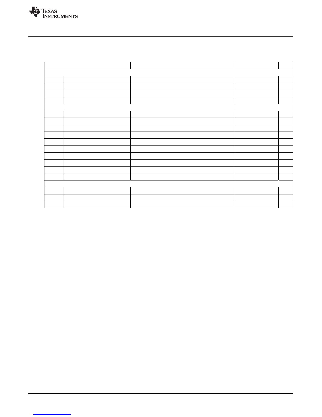
2 Electrical Performance Specifications
Table 1. TPS53127EVM-614 Electrical and Performance Specifications
Parameter Notes and Conditions MIN TYP MAX UNIT
INPUT CHARACTERISTICS
V
IN
I
IN
V
IN_UVLO
OUTPUT CHARACTERISTICS
V
OUT1
V
OUT1_rip
I
OUT1
V
OUT2
V
OUT2_rip
I
OUT2
SYSTEMS CHARACTERISTICS
F
SW
ηpk Peak Efficiency VIN= 12 V – 85% –
η Full Load Efficiency VIN= 12 V, I
Input Voltage 8 12 22 V
Input Current VIN= 12 V, I
No Load Input Current VIN= 12 V, I
Input UVLO I
= 4 A 4.0 4.2 4.5 V
OUT
Output Voltage 1 VIN= 12 V, I
Line Regulation VIN= 8 V to 22 V – – 1%
Load Regulation I
= 0 A to 4 A – – 1%
OUT1
Output Voltage Ripple VIN= 12 V, I
Output Current 1 VIN= 8 V to 22 V 0 4 A
Output Voltage 2 VIN= 12 V, I
Line Regulation VIN= 8 V to 22 V – – 1%
Load Regulation I
= 0 A to 4 A – – 1%
OUT2
Output Voltage Ripple VIN= 12 V, I
Output Current 2 VIN= 8 V to 22 V 0 4 A
Switching Frequency 350 700 800 kHz
Electrical Performance Specifications
= 4 A, I
OUT1
= 0 A – 20 35 mA
OUT
= 2 A 1.03 1.05 1.07 V
OUT1
= 4 A – - 30 mVpp
OUT2
= 2 A 1.78 1.80 1.82 V
OUT2
= 4 A – – 30 mVpp
OUT2
= 4 A – 83% –
OUT1
= 4 A – 1.2 1.5 A
OUT2
SLVU434–February 2011 TPS53127EVM-614
Submit Documentation Feedback
3
© 2011, Texas Instruments Incorporated
Page 4
+
+
+
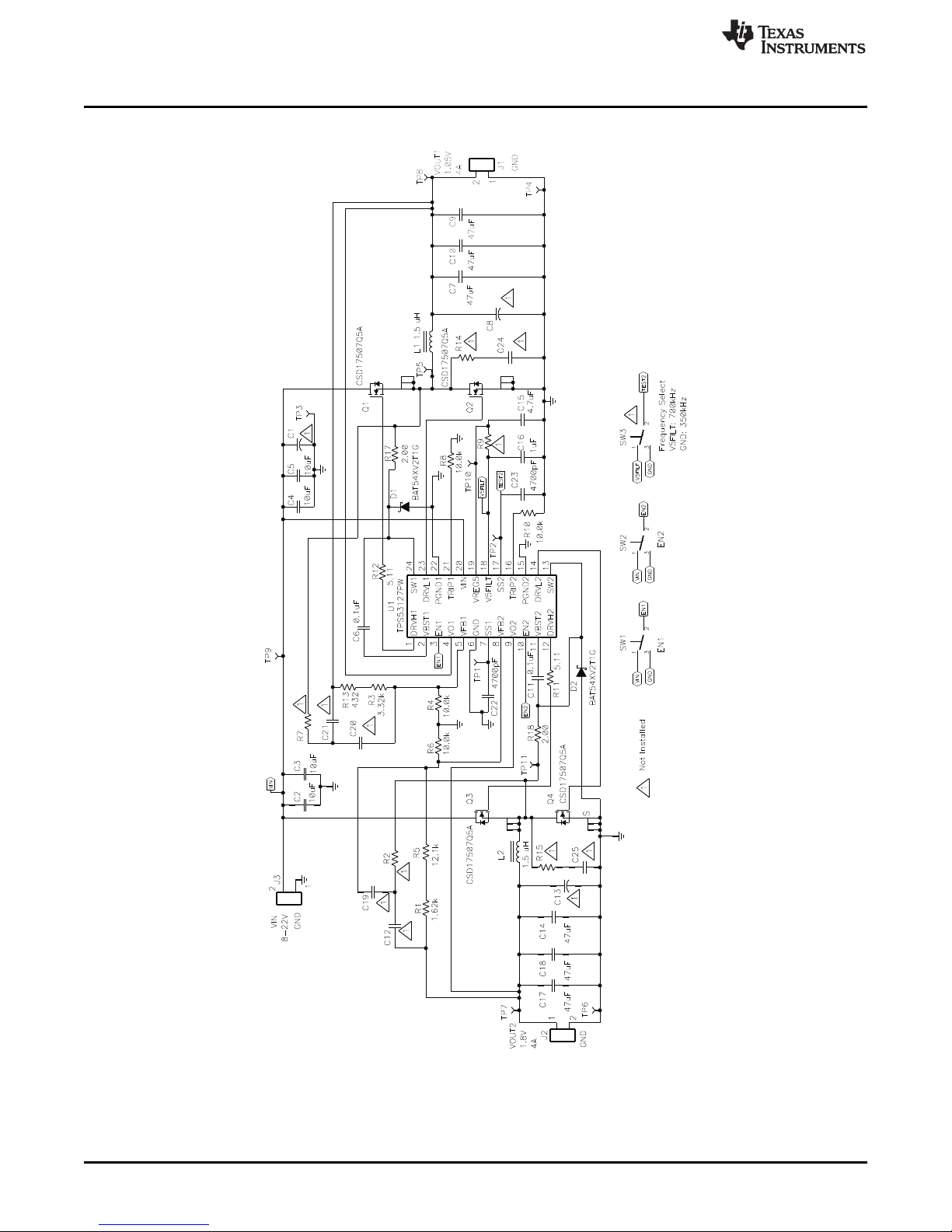
TPS53127EVM-614 Schematic
3 TPS53127EVM-614 Schematic
www.ti.com
NOTE: For Reference Only, See Table 3 for Specific Values.
Figure 1. TPS53127EVM-614 Schematic
4
TPS53127EVM-614 SLVU434–February 2011
© 2011, Texas Instruments Incorporated
Submit Documentation Feedback
Page 5
www.ti.com
4 Connector and Test Point Descriptions
4.1 Enable Switches (SW1 and SW2)
TPS53127EVM-614 includes independent enable switches for each of the two outputs. When the switch is
in the DIS position, the channel is disabled and discharged per the TPS53127’s internal discharge
characteristics.
To Enable VOUT1, place SW1 in the EN position
To Enable VOUT2, place SW2 in the EN position
4.2 Switching Frequency Select Switch (SW3)
TPS53127EVM-614 does not populate SW3. When using TPS53127EVM-614 to evaluate the TPS53126
controller in the TSSOP package, SW3 can be populated to allow selection of the TPS53126 switching
frequency between 350 kHz and 700 kHz.
4.3 Test Point Descriptions
Table 2 lists the test points, their labels, uses, and where additional information is located.
Table 2. TPS53127EVM-614 Test Points Description
Test Point Label Use Section
TP1 TEST1 Monitor Channel 1 Soft-Start Voltage Section 4.3.4
TP2 TEST2 Monitor Channel 2 Soft-Start Voltage Section 4.3.4
TP3 GND Ground for Input Voltage Section 4.3.1
TP4 GND Ground for Channel 1 Output Voltage Section 4.3.2
TP5 SW1 Monitor Switching Node for Channel 1 Section 4.3.5
TP6 GND Ground for Channel 2 Output Voltage Section 4.3.3
TP7 VO2 Monitor Output Voltage for Channel 2 Section 4.3.3
TP8 VO1 Monitor Output Voltage for Channel 1 Section 4.3.2
TP9 VIN Monitor Input Voltage Section 4.3.1
TP10 VREG5 Monitor Output of VREG5 Regulator Section 4.3.6
TP11 SW2 Monitor Switching Node for Channel 2 Section 4.3.5
CN1 VOUT1 Monitor Output Voltage for Channel 1 Section 4.3.2
CN2 VOUT2 Monitor Output Voltage for Channel 2 Section 4.3.3
Connector and Test Point Descriptions
4.3.1 Input Voltage Monitoring (TP3 and TP9)
TPS53127EVM-614 provides two test points for measuring the voltage applied to the module. This allows
the user to measure the actual module voltage without losses from input cables and connectors. All input
voltage measurements should be made between TP9 and TP3. To use TP9 and TP3, connect a voltmeter
positive terminal to TP9 and negative terminal to TP3.
4.3.2 Channel 1 Output Voltage Monitoring (TP4 and TP8)
TPS53127EVM-614 provides two test points for measuring the voltage generated at the VO1 Output by
the module. This allows the user to measure the actual output voltage without losses from output cables
and connectors. All DC Output voltage measurements should be made between TP8 and TP4. To use
TP8 and TP4, connect a voltmeter positive terminal to TP8 and negative terminal to TP4.
SLVU434–February 2011 TPS53127EVM-614
Submit Documentation Feedback
5
© 2011, Texas Instruments Incorporated
Page 6

TP4TP8
Metal Ground Barrel
Probe Tip
Test Setup
Figure 2. Tip and Barrel Measurement for Output Voltage Ripple
4.3.3 Channel 2 Output Voltage Monitoring (TP6 and TP7)
TPS53127EVM-614 provides two test points for measuring the voltage generated at the VO1 Output by
the module. This allows the user to measure the actual output voltage without losses from output cables
and connectors. All DC Output voltage measurements should be made between TP7 and TP6. To use
TP7 and TP6, connect a voltmeter positive terminal to TP7 and negative terminal to TP6.
4.3.4 Soft-Start Voltage Monitoring (TP1, TP2 and TP3)
TPS53127EVM-614 provides two test points for measuring the soft-start ramp voltages. TP1 monitors the
soft-start ramp of Channel 1. TP2 monitors the soft-start ramp of Channel 2. To use TP1 or TP2, connect
an oscilloscope probe between TP1 or TP2 and TP3.
www.ti.com
4.3.5 Switching Node Monitoring (TP3, TP5 and TP11)
TPS53127EVM-614 provides two test points for measuring the switching node waveform voltages. TP5
monitors the switching node of Channel 1. TP2 monitors the switching node of Channel 2. To use TP5 or
TP11, connect an oscilloscope probe between TP5 or TP11 and TP3.
4.3.6 5-V Regulator Output Monitoring (TP3 and TP10)
TPS53127EVM-614 provides a test point for measuring the output of the internal 5V regulator. TP10
monitors the output voltage of the internal 5V regulator. To use TP10, connect a voltmeter positive
terminal to TP10 and negative terminal to TP3.
5 Test Setup
5.1 Equipment
5.1.1 Voltage Source
V
The input voltage source (V
minimum
5.1.2 Meters
A1: 0-4Adc, Ammeter
V1: VIN, 0-22V voltmeter
V2: VOUT1, 0-2V voltmeter
V3: VOUT2, 0-2V voltmeter
IN
) shall be a 0-25V variable DC source capable of supplying 3.0 Adc
VIN
6
TPS53127EVM-614 SLVU434–February 2011
© 2011, Texas Instruments Incorporated
Submit Documentation Feedback
Page 7

www.ti.com
5.1.3 Loads
LOAD1: The Output Load shall be an Electronic Load set for Constant Current Mode capable of 0-4Adc at
1.05Vdc
LOAD2: The Output Load shall be an Electronic Load set for Constant Current Mode capable of 0-4Adc at
1.80Vdc
5.1.4 Oscilloscope
Oscilloscope
The Oscilloscope shall be an Analog or Digital Oscilloscope set for AC coupled measurement with 20MHz
bandwidth Limiting. Use 20mV / division vertical resolution, 1.0µs / division horizontal resolution for Output
Ripple Voltage Test. Set Cursors at +20mV and –20mV
Probe
One Oscilloscope probes shall be Tektronix P6138 or equivalent oscilloscope probe with exposed
conductive ground barrels.
5.1.5 Recommended Wire Gauge
VINto J3 – The connection between the source voltage, VVIN and J1 of TPS53127EVM-614 can carry as
much as 2.0Adc. The minimum recommended wire size is AWG #16 with the total length of wire less than
2 feet (1 foot input, 1 foot return).
J1 to LOAD1 and J2 to LOAD2 – The connection between J1 and LOAD1 and J2 and LOAD2 of
TPS53127EVM-614 can carry as much as 4Adc each. The minimum recommended wire size is AWG #14,
with the total length of wire less than 2 feet (1 foot input, 1 foot return)
Test Setup
5.1.6 Other
FAN – The TPS53127EVM-614 Evaluation Module includes components that can get hot to the touch.
Because this EVM is not enclosed to allow probing of circuit nodes, a small fan capable of 200-400 lfm is
required to reduce component temperatures when operating
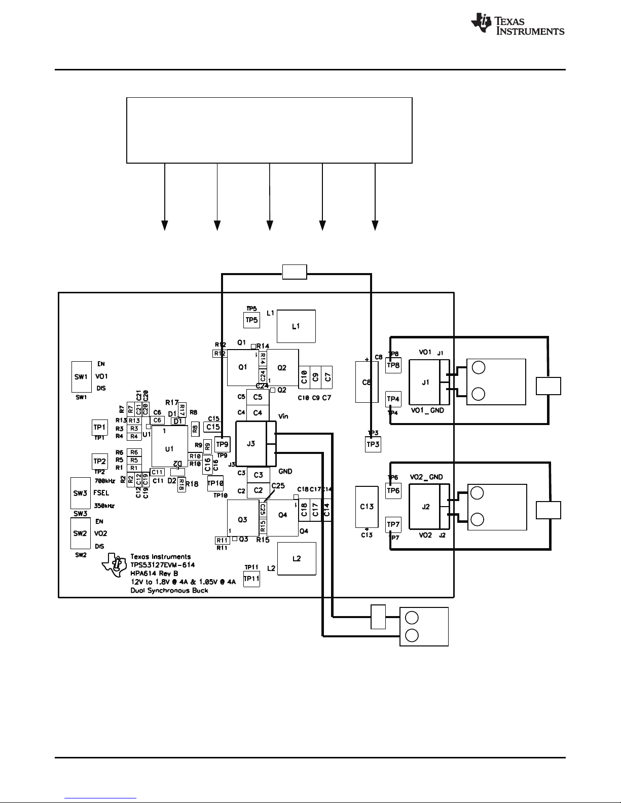
5.2 Equipment Setup
Shown in Figure 3 is the basic test set up recommended to evaluate the TPS53127EVM-614. Note that
although the return for J3 and J1 and JP2 are the same system ground, the connections should remain
separate as shown in Figure 3.
5.2.1 Procedure
1. Working at an ESD workstation, make sure that any wrist straps, bootstraps or mats are connected
referencing the user to earth ground before power is applied to the EVM. Electrostatic smock and
safety glasses should also be worn.
2. Prior to connecting the DC input source, VIN, it is advisable to limit the source current from VINto 3.0A
maximum. Make sure VINis initially set to 0V and connected as shown in Figure 3.
3. Verify SW1 and SW2 are in the desired position.
4. Place a fan as shown in Figure 3 and turn on, making sure that air is flowing across the EVM.
SLVU434–February 2011 TPS53127EVM-614
Submit Documentation Feedback
7
© 2011, Texas Instruments Incorporated
Page 8
LOAD1
1.05V @
4A
V2
+
-
LOAD2
1.8V @
4A
V3
-
+
-
+
-
+
A1
-
+
V
VIN
V1
+
-
FAN
Test Setup
5.2.2 Diagram
www.ti.com
Figure 3. TPS53127EVM-614 Recommended Test Setup
8
TPS53127EVM-614 SLVU434–February 2011
© 2011, Texas Instruments Incorporated
Submit Documentation Feedback
Page 9

www.ti.com
5.3 Start Up/Shut Down Procedure
Increase VINfrom 0V to 12Vdc
Vary LOAD1 from 0 – 4Adc
Vary LOAD2 from 0 – 4Adc
Vary VINfrom 8Vdc to 22Vdc
Decrease VINto 0Vdc
Decrease LOAD1 to 0A
Decrease LOAD2 to 0A
5.4 Output Ripple Voltage Measurement Procedure
Increase VINfrom 0V to 12Vdc
Adjust LOAD1 to desired load between 0Adc and 4Adc
Adjust LOAD2 to desired load between 0Adc and 4Adc
Adjust VINto desired load between 8Vdc and 22Vdc
Connect Oscilloscope Probe to CN1 or CN2 shown in Figure 3
Measure Output Ripple
Decrease VINto 0Vdc
Decrease LOAD1 to 0A
Decrease LOAD2 to 0A
TPS53127EVM-614 Test Data
5.5 Equipment Shutdown
Shut Down Oscilloscope
Shut down V
IN
Shut down LOAD1
Shut down LOAD2
Shut down FAN
6 TPS53127EVM-614 Test Data
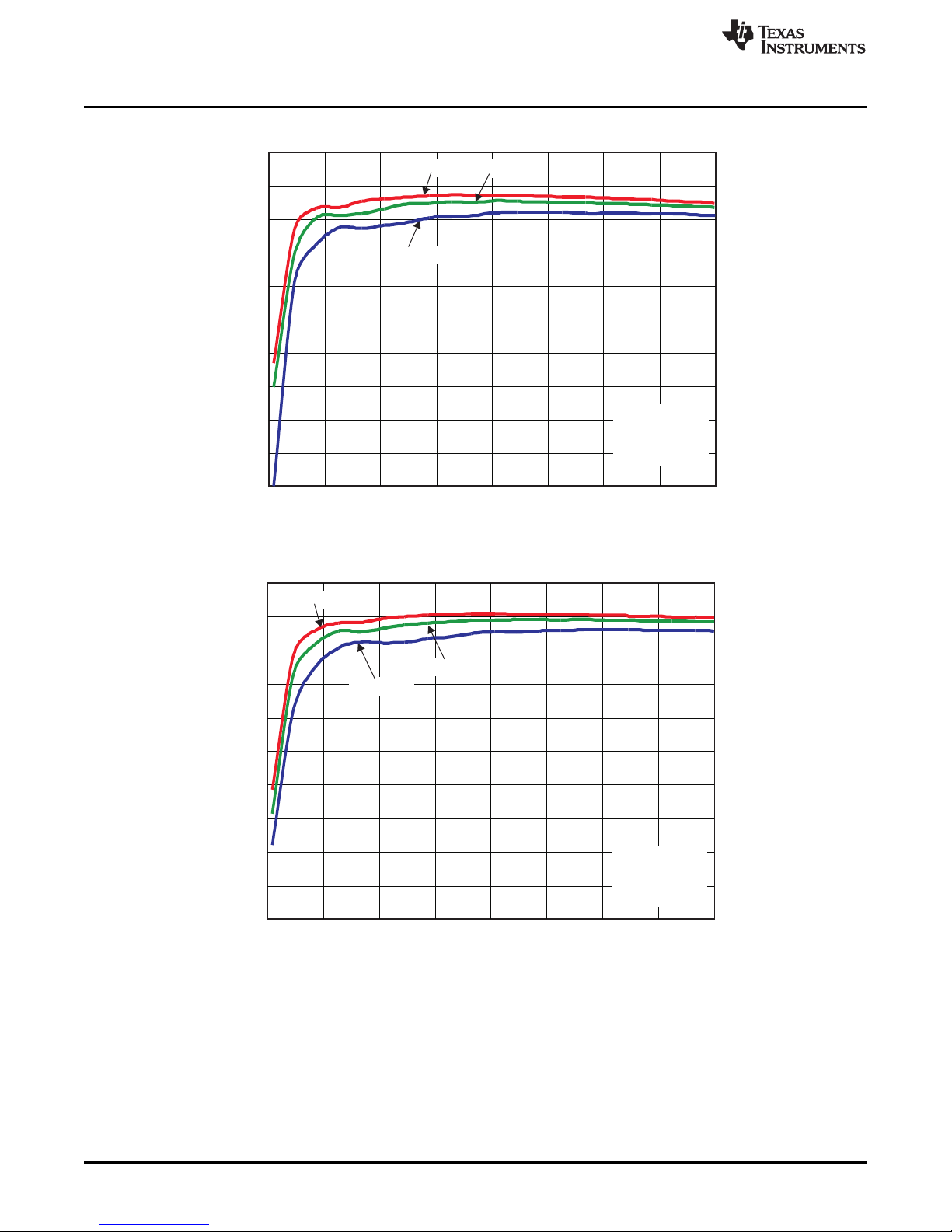
Figure 4 through Figure 11 present typical performance curves for the TPS53127EVM-614. Since actual
performance data can be affected by measurement techniques and environmental variables, these curves
are presented for reference and may differ from actual field measurements.
SLVU434–February 2011 TPS53127EVM-614
Submit Documentation Feedback
9
© 2011, Texas Instruments Incorporated
Page 10
0 0.5 1 1.5 2 2.5 3 3.5 4
I - Load Current - A
LOAD
h - Efficiency - %
0
10
20
30
40
50
60
70
80
90
100
V = 8 V
I
V = 12 V
I
V = 22 V
I
V = 8 V-22 V,
V = 1.05 V,
I = 0 A-4 A
I
OUT1
OUT1
0 0.5 1 1.5 2 2.5 3 3.5 4
I - Load Current - A
LOAD
h - Efficiency - %
0
10
20
30
40
50
60
70
80
90
100
V = 8 V
I
V = 12 V
I
V = 22 V
I
V = 8 V-22 V,
V = 1.80 V,
I = 0 A-4 A
I
OUT2
OUT2
TPS53127EVM-614 Test Data
6.1 Efficiency
www.ti.com
Figure 4. Efficiency vs Load (VIN= 8 V–22 V, V
Figure 5. Efficiency vs Load (VIN= 8 V–22 V, V
= 1.05 V, I
OUT1
OUT2
= 1.8 V, I
OUT1
OUT2
- 0 A–4A)
- 0 A–4A)
10
TPS53127EVM-614 SLVU434–February 2011
© 2011, Texas Instruments Incorporated
Submit Documentation Feedback
Page 11
I - Load Current - A
LOAD
V - Output Voltage - V
O
1.036
1.038
1.04
1.042
1.044
1.046
1.048
1.05
1.052
1.054
0 1 2 3 4
V = 22 V
I
V = 8 V
I
V = 12 V
I
V = 8 V-22 V,
V = 1.05 V,
I = 0 A-4 A
I
OUT1
OUT1
I - Load Current - A
LOAD
V - Output Voltage - V
O
1.795
1.8
1.805
1.81
1.815
1.82
1.825
1.83
0 0.5 1 1.5 2 2.5 3 3.5 4
V = 22 V
I
V = 8 V
I
V = 12 V
I
V = 8 V-22 V,
V = 1.0 V,
I = 0 A-4 A
I
OUT1
OUT1
www.ti.com
6.2 Line and Load Regulation
TPS53127EVM-614 Test Data
Figure 6. Output Voltage vs Load (VIN= 8 V–22 V, V
Figure 7. Output Voltage vs Load (VIN= 8 V–22 V, V
OUT1
OUT2
= 1.05 V, I
= 1.05 V, I
= 0 A–4 A)
OUT1
= 0 A–4 A)
OUT2
SLVU434–February 2011 TPS53127EVM-614
Submit Documentation Feedback
11
© 2011, Texas Instruments Incorporated
Page 12
TPS53127EVM-614
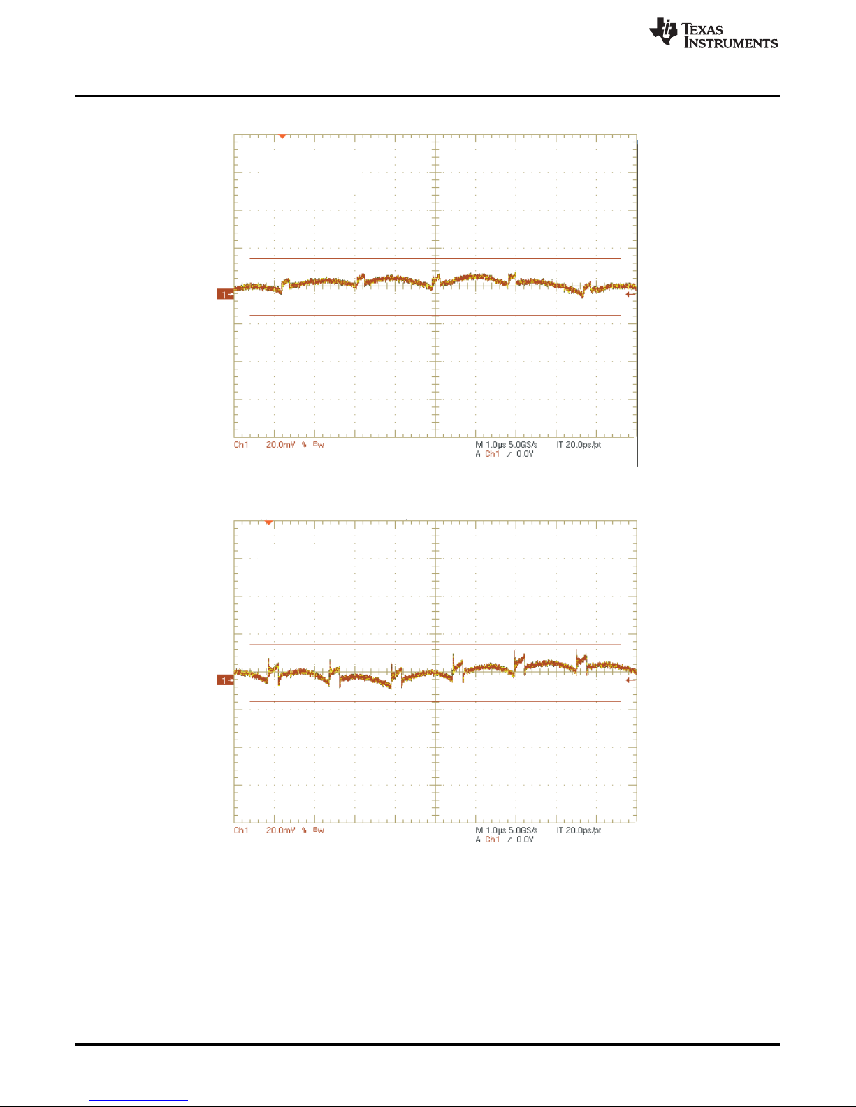
Output Ripple
Test condition: 12 Vin, 105 V/4 A
TPS53127EVM-614
Output Ripple
Test condition: 12 Vin, 1.8 V/4 A
TPS53127EVM-614 Test Data
6.3 Output Voltage Ripple and Switching Node waveforms
www.ti.com
Figure 8. Output Voltage Ripple (VIN= 12 V, V
Figure 9. Output Voltage Ripple (VIN= 12 V, V
= 1.05 V, I
OUT1
OUT2
= 1.8 V, I
OUT1
OUT2
= 4 A)
= 4 A)
12
TPS53127EVM-614 SLVU434–February 2011
© 2011, Texas Instruments Incorporated
Submit Documentation Feedback
Page 13
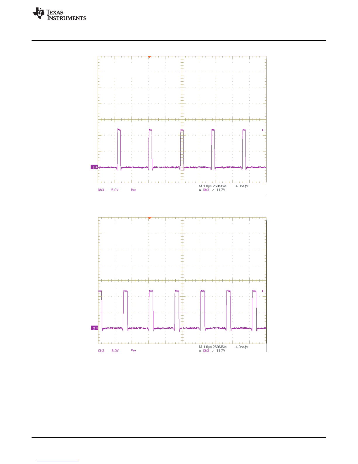
TPS53127EVM-614
SwitchNode
Test condition: 12 Vin, 1.05 V/4 A
TPS53127EVM-614
Switch Node
Test condition: 12 Vin, 1.8 V/4 A
www.ti.com
6.4 Switch Node
TPS53127EVM-614 Test Data
Figure 10. Switching Waveform (VIN= 12 V, V
Figure 11. Switching Waveform (VIN= 12 V, V
= 1.05 V, I
OUT1
OUT2
= 1.8 V, I
OUT1
OUT2
= 4 A)
= 4 A)
SLVU434–February 2011 TPS53127EVM-614
Submit Documentation Feedback
13
© 2011, Texas Instruments Incorporated
Page 14

TPS53127EVM-614 EVM Assembly Drawings and Layout
7 TPS53127EVM-614 EVM Assembly Drawings and Layout
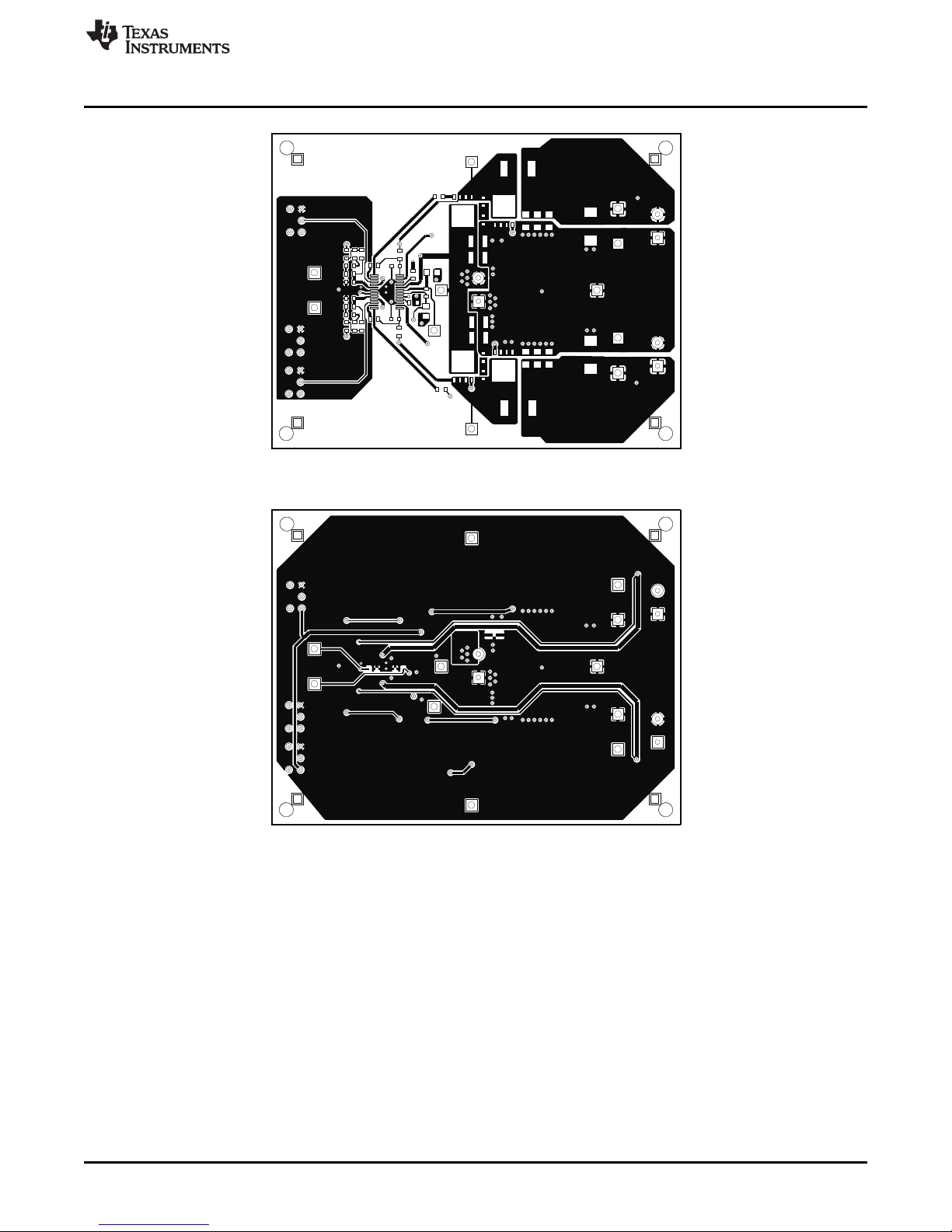
The following figures (Figure 12 through Figure 16) show the design of the TPS53127EVM-614 printed
circuit board. The EVM has been designed using a 4-Layer, 2oz copper-clad circuit board 3.5 in 2.7 to
allow the user to easily view, probe and evaluate the TPS53127 control IC in a practical application.
Moving components to both sides of the PCB or using additional internal layers can offer additional size
reduction for space constrained systems.
www.ti.com
Figure 12. Top Assembly
Figure 13. Bottom Assembly
14
TPS53127EVM-614 SLVU434–February 2011
© 2011, Texas Instruments Incorporated
Submit Documentation Feedback
Page 15
www.ti.com
TPS53127EVM-614 EVM Assembly Drawings and Layout
Figure 14. Top Layer
SLVU434–February 2011 TPS53127EVM-614
Submit Documentation Feedback
Figure 15. Bottom Layer
15
© 2011, Texas Instruments Incorporated
Page 16

TPS53127EVM-614 EVM Assembly Drawings and Layout
Figure 16. Internal Layer 1
www.ti.com
16
TPS53127EVM-614 SLVU434–February 2011
Figure 17. Internal Layer 2
Submit Documentation Feedback
© 2011, Texas Instruments Incorporated
Page 17

www.ti.com
8 Bill of Materials
Table 3 contains the Bill of Materials for TPS53127EVM-614. The reference designators reference the
Schematic in Figure 1 and Assembly locations in Figure 12. Components with a Quantity 0 listed are not
populated on the PCB but are provided for reference.
Table 3. TPS53127EVM-614 Bill of Materials
Count RefDes Value Description Size Part Number MFR
0 C1 Capacitor, Aluminum, 25V, 20% 0.328 x 0.390 inch Std Std
0 C12, C19, C20, Capacitor, Ceramic 0603 Std Std
C21
1 C15 4.7 µF Capacitor,Ceramic, 10V, X5R, 20% 0805 Std Std
1 C16 1 µF Capacitor, Ceramic, 16V, X5R, 20% 0805 Std Std
4 C2, C3, C4, C5 10 µF Capacitor, Ceramic, 25V, X5R, 20% 1210 Std Std
2 C22, C23 4700pF Capacitor, Ceramic, Low Inductance, 16V, 0603 Std Std
0 C24, C25 Capacitor, Ceramic, 25V, X7R, 20% 0603 Std Std
2 C6, C11 0.1 µF Capacitor, Ceramic, 50V, X5R, 10% 0603 Std Std
6 C7, C9, C10, C14, 47 µF Capacitor, Ceramic, 6.3V, X5R, 20% 1206 Std Std
C17, C18
0 C8, C13 330 µF Capacitor, PXE, 4.0V, 15 milliohm, 20% 7343 (D) APXE4R0ARA331MF61G NIPPON
2 D1, D2 BAT54XV2T1G Diode, Schottky, 200 mA, 30 V SOD523 BAT54XV2T1G On Semi
3 J1, J2, J3 ED120/2DS Terminal Block, 2-pin, 15-A, 5.1mm 0.40 x 0.35 inch ED120/2DS OST
2 L1, L2 1.5 µH Inductor, SMT, 11A, 9.7 milliohm 0.256x 0.280 inch SPM6530T-1R5M100 TDK
4 Q1, Q2, Q3, Q4 CSD17507Q5A MOSFET,N-Chan, 30V, 65A, 11.8 milliohm QFN-8 POWER CSD17507Q5A TI
1 R1 1.62k Resistor, Chip, 1/16W, 1% 0603 Std Std
4 R10, R4, R6, R8 10.0k Resistor, Chip, 1/16W, 1% 0603 Std Std
2 R11, R12 5.11 Resistor, Chip, 1/16W, 1% 0603 Std Std
1 R13 432 Resistor, Chip, 1/16W, 1% 0603 Std Std
0 R14, R15 Resistor, Chip, 1/8W, 5% 0603 Std Std
2 R17, R18 2.00 Resistor, Chip, 1/16W, 1% 0603 Std Std
0 R2, R7, R9 Resistor, Chip, 1/16W, 1% 0603 Std Std
1 R3 3.32k Resistor, Chip, 1/16W, 1% 0603 Std Std
1 R5 12.1k Resistor, Chip, 1/16W, 1% 0603 Std Std
2 SW1, SW2 G12AP-RO Switch, ON-ON Mini Toggle 0.28 x 0.18"" G12AP-RO Nikkai
0 SW3 G12AP-RO Switch, ON-ON Mini Toggle 0.28 x 0.18"" G12AP-RO Nikkai
4 TP1, TP2, TP5, 5012 Test Point, White, Thru Hole 0.125 x 0.125 inch 5012 Keystone
TP11
1 TP10 5013 Test Point, Orange, Thru Hole 0.125 x 0.125 inch 5013 Keystone
3 TP3, TP4, TP6 5011 Test Point, Black, Thru Hole 0.125 x 0.125 inch 5011 Keystone
2 TP7, TP8 5014 Test Point, Yellow, Thru Hole 0.125 x 0.125 inch 5014 Keystone
1 TP9 5010 Test Point, Red, Thru Hole 0.125 x 0.125 inch 5010 Keystone
1 U1 TPS53127PW IC, Dual Synchronous Step-Down Controller TSSOP TPS53127PW TI
1 – PCB, 2.70" x 3.50" x 0.063" FR-4 2.7" x 3.5" HPA614 Any
Notes: 1. These assemblies are ESD sensitive, ESD precautions shall be observed.
2. These assemblies must be clean and free from flux and all contaminants. Use of no clean flux is not acceptable.
3. These assemblies must comply with workmanship standards IPC-A-610 Class 2.
4. Ref designators marked with an asterisk ('**') cannot be substituted. All other components can be substituted with equivalent MFG's components.
X7R, 20%
For Low-Voltage Power Rails
Bill of Materials
CHEMI-CON
SLVU434–February 2011 TPS53127EVM-614
Submit Documentation Feedback
17
© 2011, Texas Instruments Incorporated
Page 18

Evaluation Board/Kit Important Notice
Texas Instruments (TI) provides the enclosed product(s) under the following conditions:
This evaluation board/kit is intended for use for ENGINEERING DEVELOPMENT, DEMONSTRATION, OR EVALUATION
PURPOSES ONLY and is not considered by TI to be a finished end-product fit for general consumer use. Persons handling the
product(s) must have electronics training and observe good engineering practice standards. As such, the goods being provided are
not intended to be complete in terms of required design-, marketing-, and/or manufacturing-related protective considerations,
including product safety and environmental measures typically found in end products that incorporate such semiconductor
components or circuit boards. This evaluation board/kit does not fall within the scope of the European Union directives regarding
electromagnetic compatibility, restricted substances (RoHS), recycling (WEEE), FCC, CE or UL, and therefore may not meet the
technical requirements of these directives or other related directives.
Should this evaluation board/kit not meet the specifications indicated in the User’s Guide, the board/kit may be returned within 30
days from the date of delivery for a full refund. THE FOREGOING WARRANTY IS THE EXCLUSIVE WARRANTY MADE BY
SELLER TO BUYER AND IS IN LIEU OF ALL OTHER WARRANTIES, EXPRESSED, IMPLIED, OR STATUTORY, INCLUDING
ANY WARRANTY OF MERCHANTABILITY OR FITNESS FOR ANY PARTICULAR PURPOSE.
The user assumes all responsibility and liability for proper and safe handling of the goods. Further, the user indemnifies TI from all
claims arising from the handling or use of the goods. Due to the open construction of the product, it is the user’s responsibility to
take any and all appropriate precautions with regard to electrostatic discharge.
EXCEPT TO THE EXTENT OF THE INDEMNITY SET FORTH ABOVE, NEITHER PARTY SHALL BE LIABLE TO THE OTHER
FOR ANY INDIRECT, SPECIAL, INCIDENTAL, OR CONSEQUENTIAL DAMAGES.
TI currently deals with a variety of customers for products, and therefore our arrangement with the user is not exclusive.
TI assumes no liability for applications assistance, customer product design, software performance, or infringement of
patents or services described herein.
Please read the User’s Guide and, specifically, the Warnings and Restrictions notice in the User’s Guide prior to handling the
product. This notice contains important safety information about temperatures and voltages. For additional information on TI’s
environmental and/or safety programs, please contact the TI application engineer or visit www.ti.com/esh.
No license is granted under any patent right or other intellectual property right of TI covering or relating to any machine, process, or
combination in which such TI products or services might be or are used.
FCC Warning
This evaluation board/kit is intended for use for ENGINEERING DEVELOPMENT, DEMONSTRATION, OR EVALUATION
PURPOSES ONLY and is not considered by TI to be a finished end-product fit for general consumer use. It generates, uses, and
can radiate radio frequency energy and has not been tested for compliance with the limits of computing devices pursuant to part 15
of FCC rules, which are designed to provide reasonable protection against radio frequency interference. Operation of this
equipment in other environments may cause interference with radio communications, in which case the user at his own expense
will be required to take whatever measures may be required to correct this interference.
EVM Warnings and Restrictions
It is important to operate this EVM within the input voltage range of 8.0 V to 22V and the output voltage range of 1.03 V to 1.90 V .
Exceeding the specified input range may cause unexpected operation and/or irreversible damage to the EVM. If there are
questions concerning the input range, please contact a TI field representative prior to connecting the input power.
Applying loads outside of the specified output range may result in unintended operation and/or possible permanent damage to the
EVM. Please consult the EVM User's Guide prior to connecting any load to the EVM output. If there is uncertainty as to the load
specification, please contact a TI field representative.
During normal operation, some circuit components may have case temperatures greater than 40° C. The EVM is designed to
operate properly with certain components above 40° C as long as the input and output ranges are maintained. These components
include but are not limited to linear regulators, switching transistors, pass transistors, and current sense resistors. These types of
devices can be identified using the EVM schematic located in the EVM User's Guide. When placing measurement probes near
these devices during operation, please be aware that these devices may be very warm to the touch.
Mailing Address: Texas Instruments, Post Office Box 655303, Dallas, Texas 75265
Copyright © 2011, Texas Instruments Incorporated
Page 19

IMPORTANT NOTICE
Texas Instruments Incorporated and its subsidiaries (TI) reserve the right to make corrections, modifications, enhancements, improvements,
and other changes to its products and services at any time and to discontinue any product or service without notice. Customers should
obtain the latest relevant information before placing orders and should verify that such information is current and complete. All products are
sold subject to TI’s terms and conditions of sale supplied at the time of order acknowledgment.
TI warrants performance of its hardware products to the specifications applicable at the time of sale in accordance with TI’s standard
warranty. Testing and other quality control techniques are used to the extent TI deems necessary to support this warranty. Except where
mandated by government requirements, testing of all parameters of each product is not necessarily performed.
TI assumes no liability for applications assistance or customer product design. Customers are responsible for their products and
applications using TI components. To minimize the risks associated with customer products and applications, customers should provide
adequate design and operating safeguards.
TI does not warrant or represent that any license, either express or implied, is granted under any TI patent right, copyright, mask work right,
or other TI intellectual property right relating to any combination, machine, or process in which TI products or services are used. Information
published by TI regarding third-party products or services does not constitute a license from TI to use such products or services or a
warranty or endorsement thereof. Use of such information may require a license from a third party under the patents or other intellectual
property of the third party, or a license from TI under the patents or other intellectual property of TI.
Reproduction of TI information in TI data books or data sheets is permissible only if reproduction is without alteration and is accompanied
by all associated warranties, conditions, limitations, and notices. Reproduction of this information with alteration is an unfair and deceptive
business practice. TI is not responsible or liable for such altered documentation. Information of third parties may be subject to additional
restrictions.
Resale of TI products or services with statements different from or beyond the parameters stated by TI for that product or service voids all
express and any implied warranties for the associated TI product or service and is an unfair and deceptive business practice. TI is not
responsible or liable for any such statements.
TI products are not authorized for use in safety-critical applications (such as life support) where a failure of the TI product would reasonably
be expected to cause severe personal injury or death, unless officers of the parties have executed an agreement specifically governing
such use. Buyers represent that they have all necessary expertise in the safety and regulatory ramifications of their applications, and
acknowledge and agree that they are solely responsible for all legal, regulatory and safety-related requirements concerning their products
and any use of TI products in such safety-critical applications, notwithstanding any applications-related information or support that may be
provided by TI. Further, Buyers must fully indemnify TI and its representatives against any damages arising out of the use of TI products in
such safety-critical applications.
TI products are neither designed nor intended for use in military/aerospace applications or environments unless the TI products are
specifically designated by TI as military-grade or "enhanced plastic." Only products designated by TI as military-grade meet military
specifications. Buyers acknowledge and agree that any such use of TI products which TI has not designated as military-grade is solely at
the Buyer's risk, and that they are solely responsible for compliance with all legal and regulatory requirements in connection with such use.
TI products are neither designed nor intended for use in automotive applications or environments unless the specific TI products are
designated by TI as compliant with ISO/TS 16949 requirements. Buyers acknowledge and agree that, if they use any non-designated
products in automotive applications, TI will not be responsible for any failure to meet such requirements.
Following are URLs where you can obtain information on other Texas Instruments products and application solutions:
Products Applications
Audio www.ti.com/audio Communications and Telecom www.ti.com/communications
Amplifiers amplifier.ti.com Computers and Peripherals www.ti.com/computers
Data Converters dataconverter.ti.com Consumer Electronics www.ti.com/consumer-apps
DLP® Products www.dlp.com Energy and Lighting www.ti.com/energy
DSP dsp.ti.com Industrial www.ti.com/industrial
Clocks and Timers www.ti.com/clocks Medical www.ti.com/medical
Interface interface.ti.com Security www.ti.com/security
Logic logic.ti.com Space, Avionics and Defense www.ti.com/space-avionics-defense
Power Mgmt power.ti.com Transportation and www.ti.com/automotive
Microcontrollers microcontroller.ti.com Video and Imaging www.ti.com/video
RFID www.ti-rfid.com Wireless www.ti.com/wireless-apps
RF/IF and ZigBee® Solutions www.ti.com/lprf
TI E2E Community Home Page e2e.ti.com
Automotive
Mailing Address: Texas Instruments, Post Office Box 655303, Dallas, Texas 75265
Copyright © 2011, Texas Instruments Incorporated
 Loading...