

Page 1

TPS53119EVM-690 User Guide
The TPS53119EVM-690 evaluation module allows users to evaluate the Texas Instruments TPS53119, a
small-sized, single, buck controller with adaptive on-time D-CAP™ mode control. Included in this
document are operating and testing descriptions as well as the EVM schematic, bill of materials, and
board layout.
Contents
1 Introduction ................................................................................................................... 3
2 Description.................................................................................................................... 3
2.1 Typical Applications ................................................................................................ 3
2.2 Features.............................................................................................................. 3
3 Electrical Performance Specifications..................................................................................... 4
4 Schematic..................................................................................................................... 5
5 Test Setup .................................................................................................................... 6
5.1 Test Equipment ..................................................................................................... 6
5.2 Recommended Test Setup ........................................................................................ 7
6 Configurations................................................................................................................ 7
6.1 Switching Frequency Selection .................................................................................. 7
6.2 Soft-Start Selection................................................................................................. 8
6.3 Mode Selection...................................................................................................... 8
6.4 Enable Selection.................................................................................................... 8
7 Test Procedure............................................................................................................... 9
7.1 Line/Load Regulation and Efficiency Measurement Procedure .............................................. 9
7.2 Control Loop Gain and Phase Measurement Procedure...................................................... 9
7.3 List of Test Points ................................................................................................. 10
7.4 Equipment Shutdown ............................................................................................. 10
8 Performance Data and Typical Characteristic Curves................................................................. 11
8.1 Efficiency ........................................................................................................... 11
8.2 Load Regulation ................................................................................................... 11
8.3 Output Transient................................................................................................... 12
8.4 Output Ripple ...................................................................................................... 13
8.5 Switching Node.................................................................................................... 13
8.6 Enable Turnon/Turnoff............................................................................................ 14
8.7 Output 1.1-V Prebias Turnon .................................................................................... 15
8.8 Bode Plot........................................................................................................... 15
8.9 Thermal Image..................................................................................................... 16
9 EVM Assembly Drawing and PCB Layout .............................................................................. 17
10 Bill of Materials ............................................................................................................. 21
User's Guide
SNVU589–December 2017
1 TPS53119EVM-690 Schematic............................................................................................ 5
2 Tip and Barrel Measurement for Vout Ripple ............................................................................ 6
3 TPS53119EVM-690 Recommended Test Setup ........................................................................ 7
4 Efficiency .................................................................................................................... 11
5 Load Regulation ............................................................................................................ 11
6 Output Load Transient..................................................................................................... 12
7 Output Load Transient..................................................................................................... 12
SNVU589–December 2017
Submit Documentation Feedback
List of Figures
Copyright © 2017, Texas Instruments Incorporated
TPS53119EVM-690 User Guide
1
Page 2

www.ti.com
8 Output Ripple ............................................................................................................... 13
9 Switching Node............................................................................................................. 13
10 Enable Turnon.............................................................................................................. 14
11 Enable Turnoff.............................................................................................................. 14
12 Output 1.1-V Prebias Turnon............................................................................................. 15
13 Bode Plot at 12 V
14 Top Board at 12 V
15 Bottom Board at 12 V
, 1.1 V/25 A........................................................................................... 15
IN
, 1.1 V/25 A.......................................................................................... 16
IN
, 1.1 V/25 A ..................................................................................... 16
IN
16 TPS53119EVM-690 Top Layer Assembly Drawing, Top View....................................................... 17
17 TPS53119EVM-690 Bottom Assembly Drawing, Bottom View ...................................................... 17
18 TPS53119EVM-690 Top Copper, Top View............................................................................ 18
19 TPS53119EVM-690 Layer-2 Copper, Top View ....................................................................... 18
20 TPS53119EVM-690 Layer-3 Copper, Top View ....................................................................... 19
21 TPS53119EVM-690 Layer-4 Copper, Top View ....................................................................... 19
22 TPS53119EVM-690 Layer-5 Copper, Top View ....................................................................... 20
23 TPS53119EVM-690 Bottom Layer Copper, Top View ................................................................ 20
List of Tables
1 TPS53119EVM-690 Electrical Performance Specifications............................................................ 4
2 Switching Frequency Selection ............................................................................................ 8
3 Soft-Start Selection.......................................................................................................... 8
4 MODE Selection ............................................................................................................. 8
5 Enable Selection............................................................................................................. 8
6 Functions of Each Test Points............................................................................................ 10
7 The EVM Bill of Materials According to Schematic Shown in ....................................................... 21
Trademarks
D-CAP is a trademark of Texas Instruments.
All other trademarks are the property of their respective owners.
2
TPS53119EVM-690 User Guide
Copyright © 2017, Texas Instruments Incorporated
SNVU589–December 2017
Submit Documentation Feedback
Page 3

www.ti.com
1 Introduction
The TPS53119EVM-690 evaluation module (EVM) uses the TPS53119 device. The TPS53119 is a smallsize, single buck controller with adaptive on-time D-CAP™ mode control. It provides a fixed 1.1-V output
at up to 25 A from a 12-V input bus. TPS53119EVM-690 also uses the 5-mm × 6-mm TI power block
MOSFET (CSD86350Q5D) for high power density and superior thermal performance.
2 Description
The TPS53119EVM-690 is designed to use a regulated 12-V bus to produce a regulated 1.1-V output at
up to 25 A of load current. The TPS53119EVM-690 is designed to demonstrate the TPS53119 in a typical
low-voltage application while providing test points to evaluate the performance of the TPS53119.
2.1 Typical Applications
• Point of load systems
• Storage computer
• Server computer
• Multifunction printer
• Embedded computing
2.2 Features
The TPS53119EVM-690 features:
• 25-Adc, steady-state output current
• Support prebias output voltage start-up
• High efficiency and high power density by using TI power block MOSFET
• J1 for selectable switching frequency setting
• J2 for selectable internal voltage servo soft start
• J3 for enable function
• J6 for auto-skip and forced CCM selection
• Convenient test points for probing critical waveforms
Introduction
SNVU589–December 2017
Submit Documentation Feedback
Copyright © 2017, Texas Instruments Incorporated
TPS53119EVM-690 User Guide
3
Page 4
Electrical Performance Specifications
3 Electrical Performance Specifications
Table 1. TPS53119EVM-690 Electrical Performance Specifications
www.ti.com
PARAMETER TEST CONDITIONS MIN TYP
MA
UNIT
X
INPUT CHARACTERISTICS
Voltage range V
IN
Maximum input current VIN= 8 V, I
No load input current VIN= 14 V, I
= 25 A 4 A
OUT
= 0 A with auto-skip mode 1 mA
OUT
8 12 14 V
OUTPUT CHARACTERISTICS
Output voltage VOUT 1.1 V
Output voltage regulation Line regulation(VIN= 8 V-14 V) 0.5%
Load regulation(VIN= 12 V, I
= 0 A-25 A) 0.5%
OUT
Output voltage ripple VIN= 12 V, Io = 25 A 25 mVpp
Output load current 0 25 A
Output over current 35 A
SYSTEMS CHARACTERISTICS
Switching frequency 300 kHz
Peak efficiency VIN= 12 V, 1.1 V/10 A 90.90%
Full-load efficiency VIN= 12 V, 1.1 V/25 A 88.59%
Operating temperature 25 ºC
Note: Jumpers set to default locations, See Section 6 of this user’s guide
4
TPS53119EVM-690 User Guide
Copyright © 2017, Texas Instruments Incorporated
SNVU589–December 2017
Submit Documentation Feedback
Page 5

1000KHz
650KHz
300KHz
2.8ms SS
500KHz
750KHz
850KHz
250KHz
400KHz
FCCM
AUTOSKI
P
1.4ms SS
5.6ms SS
0.7ms SS
Note:
+
+ +
www.ti.com
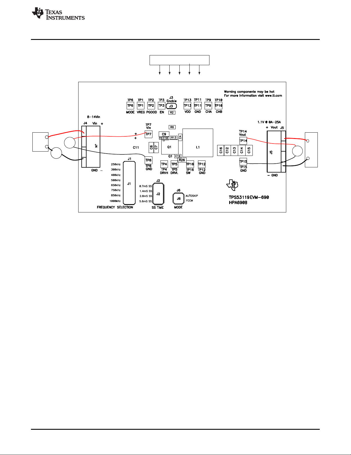
4 Schematic
Schematic
SNVU589–December 2017
Submit Documentation Feedback
Figure 1. TPS53119EVM-690 Schematic
Copyright © 2017, Texas Instruments Incorporated
TPS53119EVM-690 User Guide
5
Page 6
TP15TP14
Metal Ground Barrel
Probe Tip
Test Setup
5 Test Setup
5.1 Test Equipment
Voltage Source: The input voltage source VINmust be a 0-V to 14-V variable dc source capable of
supplying 10 Adc. Connect Vin to J4 as shown in Figure 3.
Multimeters:
V1: VINat TP7 (Vin) and TP8 (GND).
V2: V
A1: Vin input current
Output Load: The output load must be an electronic constant resistance mode load capable of 0 Adc to
30 Adc at 1.1 V.
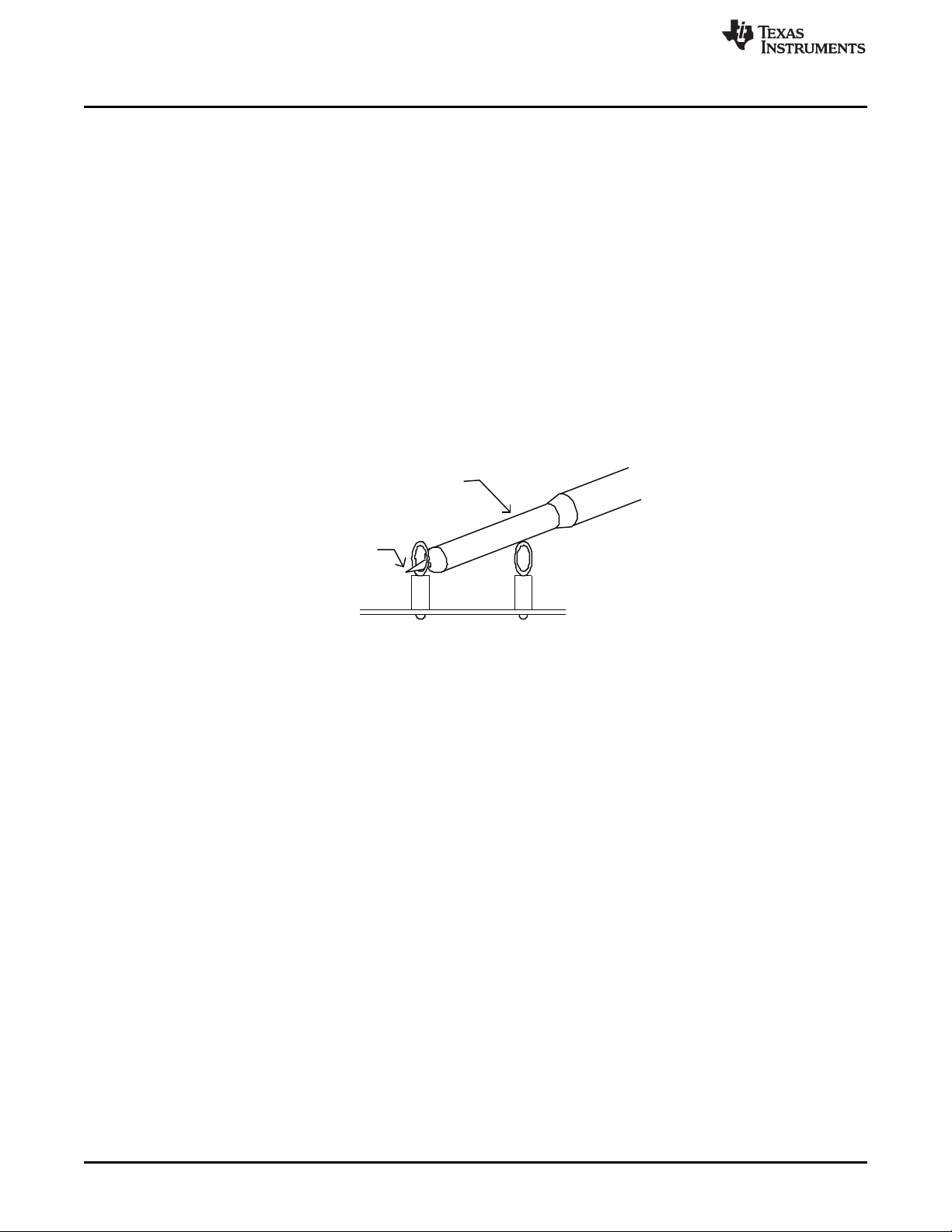
Oscilloscope: A digital or analog oscilloscope can be used to measure the output ripple. The oscilloscope
must be set for 1-MΩ impedance, 20-MHz bandwidth, ac coupling, 2-µs/division horizontal resolution, 50mV/division vertical resolution. Test points TP14 and TP15 can be used to measure the output ripple
voltage by placing the oscilloscope probe tip through TP14 and holding the ground barrel on TP15 as
shown in Figure 2. Using a leaded ground connection may induce additional noise due to the large ground
loop.
at TP14 (Vout) and TP15 (GND).
OUT
www.ti.com
Fan: Some of the components of this EVM may approach temperatures of 60°C during operation. A small
fan capable of 200-400 LFM is recommended to reduce component temperatures while the EVM is
operating. The EVM must not be probed if the fan is not running.
Recommended Wire Gauge:
1. VINto J4 (12-V input):
2. J5 to LOAD:
Figure 2. Tip and Barrel Measurement for Vout Ripple
The recommended wire size is 1 × AWG 14 per input connection, with the total length of wire less than
4 feet (2-foot input, 2-foot return).
The minimum recommended wire size is 2 × AWG 14, with the total length of wire less than 4 feet (2foot output, 2-foot return)
6
TPS53119EVM-690 User Guide
Copyright © 2017, Texas Instruments Incorporated
SNVU589–December 2017
Submit Documentation Feedback
Page 7
T
I
NSTRUMENTS
EXAS
V1
A1
DC
Source
Vin
-
Load
+
V2
FAN
+
-
www.ti.com
5.2 Recommended Test Setup
Test Setup
Figure 3. TPS53119EVM-690 Recommended Test Setup
Figure 3 is the recommended test setup to evaluate the TPS53119EVM-690. Working at an ESD
workstation, make sure that any wrist straps, bootstraps, or mats are connected referencing the user to
earth ground before power is applied to the EVM.
Input Connections:
1. Prior to connecting the dc input source VIN, it is advisable to limit the source current from VINto 10 A
maximum. Ensure that VINis initially set to 0 V and connected as shown in Figure 3.
2. Connect a voltmeter V1 at TP7 (VIN) and TP8 (GND) to measure the input voltage.
3. Connect a current meter A1 to measure the input current.
Output Connections:
1. Connect load to J5, and set Load to constant resistance mode to sink 0 Adc before VINis applied.
2. Connect a voltmeter V2 at TP14 (V
) and TP15 (GND) to measure the output voltage.
OUT
Other Connections:
Place a fan as shown in Figure 3 and turn it on, ensuring that air is flowing across the EVM.
6 Configurations
All jumper selections must be made prior to applying power to the EVM. Users can configure this EVM per
the following configurations.
6.1 Switching Frequency Selection
The switching frequency can be set by J1.
Default setting: 300 kHz
SNVU589–December 2017
Submit Documentation Feedback
Copyright © 2017, Texas Instruments Incorporated
TPS53119EVM-690 User Guide
7
Page 8

Configurations
JUMPER SET TO RESISTOR (RF) CONNECTIONS (Ω) SWITCHING FREQUENCY (kHz)
Top(1-2 pin shorted) 0 250
Second (3-4 pin shorted) 187 k 300
Third (5-6 pin shorted) 619 k 400
Fourth (7-8 pin shorted) Open 500
Fifth (9-10 pin shorted) 866 k 650
Sixth (11-12 pin shorted) 309 k 750
Seventh (13-14 pin shorted) 124 k 850
Bottom (15-16 pin shorted) 0 1000
6.2 Soft-Start Selection
The soft-start time can be set by J2.
Default setting: 0.7 ms
www.ti.com
Table 2. Switching Frequency Selection
Table 3. Soft-Start Selection
JUMPER SET TO R
Top (1-2 pin shorted) 39.2 k 0.7
Second (3-4 pin shorted) 100 k 1.4
Third (5-6 pin shorted) 200 k 2.8
Bottom (7-8 pin shorted) 475 k 5.6
6.3 Mode Selection
The MODE can be set by J6.
Default setting: Auto Skip
Top (1-2 pin shorted) Auto Skip
Bottom (3-4 pin shorted) Forced CCM
6.4 Enable Selection
The controller can be enabled and disabled by J3.
Default setting: Jumper shorts on J3 to disable the controller
CONNECTIONS (Ω) SOFT-START TIME (ms)
MODE
Table 4. MODE Selection
Jumper Set to MODE Selection
Table 5. Enable Selection
JUMPER SET TO ENABLE SELECTION
Jumper shorts on J3 Disable the controller
No Jumper shorts on J3 Enable the controller
8
TPS53119EVM-690 User Guide
Copyright © 2017, Texas Instruments Incorporated
SNVU589–December 2017
Submit Documentation Feedback
Page 9

www.ti.com
7 Test Procedure
7.1 Line/Load Regulation and Efficiency Measurement Procedure
1. Set up EVM as described in Section 5 and Figure 3.
2. Ensure that load is set to constant resistance mode and to sink 0 Adc.
3. Ensure that all jumper configuration settings per Section 6.
4. Ensure that the jumper provided in the EVM shorts on J3 before VINis applied.
5. Increase VINfrom 0 V to 12 V. Using V1 to measure input voltage.
6. Remove the jumper on J3 to enable the controller.
7. Use V2 to measure V
8. Vary Load from 0-25 Adc; V
9. Vary Vin from 8 V to 14 V, V
OUT
voltage.
must remain in load regulation.
OUT
must remain in line regulation.
OUT
10. Put the jumper on J3 to disable the controller.
11. Decrease load to 0 A.
12. Decrease VINto 0 V.
7.2 Control Loop Gain and Phase Measurement Procedure
TPS53119EVM-690 contains a 10-Ω series resistor in the feedback loop for loop response analysis.
1. Set up EVM as described in Section 5 and Figure 3.
2. Connect isolation transformer to test points marked TP9 and TP10.
3. Connect input signal amplitude measurement probe (channel A) to TP9. Connect output signal
amplitude measurement probe (channel B) to TP10.
4. Connect ground lead of channel A and channel B to TP11.
5. Inject approximately 40-mV or less signal through the isolation transformer.
6. Sweep the frequency from 100 Hz to 1 MHz with 10 Hz or lower post filter. The control loop gain and
phase margin can be measured.
7. Disconnect isolation transformer from bode plot test points before making other measurements. (Signal
injection into feedback may interfere with accuracy of other measurements.)
Test Procedure
SNVU589–December 2017
Submit Documentation Feedback
Copyright © 2017, Texas Instruments Incorporated
TPS53119EVM-690 User Guide
9
Page 10

Test Procedure
7.3 List of Test Points
TEST POINTS NAME DESCRIPTION
TP1 VREG 6.2-V LDO output
TP2 PGOOD Power Good
TP3 EN Enable pin
TP4 DRVH High-side driver output
TP5 DRVL Low-side driver output
TP6 MODE Soft-start and auto skip/FCCM selection pin
TP7 Vin V
TP8 GND GND for V
TP9 CHA Input A for loop injection
TP10 CHB Input B for loop injection
TP11 GND GND
TP12 GND GND
TP13 VDD Controller power supply input
TP14 Vout Output voltage
TP15 GND GND for output voltage
www.ti.com
Table 6. Functions of Each Test Points
IN
IN
7.4 Equipment Shutdown
1. Shut down load.
2. Shut down VIN.
3. Shut down FAN.
10
TPS53119EVM-690 User Guide
Copyright © 2017, Texas Instruments Incorporated
SNVU589–December 2017
Submit Documentation Feedback
Page 11

1.1
1.11
1.12
1.13
1.14
1.15
1.16
1.17
0.001 0.01 0.1 1 10 100
I - Output Current - A
O
12 V auto skip
I
14 V auto skip
I
8 V auto skip
I
12 V forced CCM
I
14 V forced CCM
I
8 V forced CCM
I
V - Output Voltage - V
O
0.001 0.01 0.1 1 10 100
I - Output Current - A
O
12 V auto skip
I
14 V auto skip
I
8 V forced CCM
I
8 V auto skip
I
14 V forced CCM
I
12 V forced CCM
I
0
10
20
30
40
50
60
70
80
90
100
Efficiency - %
www.ti.com
Performance Data and Typical Characteristic Curves
8 Performance Data and Typical Characteristic Curves
Figure 4 through Figure 12 present typical performance curves for TPS53119EVM-690.
8.1 Efficiency
Figure 4. Efficiency
8.2 Load Regulation
SNVU589–December 2017
Submit Documentation Feedback
Copyright © 2017, Texas Instruments Incorporated
Figure 5. Load Regulation
TPS53119EVM-690 User Guide
11
Page 12

Output Transient
Test Condition: 12 Vin, 1.1 V/0A-15 A
Auto skip mode
CH1: 1.1 Vout
CH4: 1.1 V Output Current
Output Transient
Test Condition: 12 Vin, 1.1 V/0A-15 A
Forced CCM mode
CH1: 1.1 Vout
CH4: 1.1 V Output Current
Performance Data and Typical Characteristic Curves
8.3 Output Transient
Figure 6. Output Load Transient
www.ti.com
12
TPS53119EVM-690 User Guide
Figure 7. Output Load Transient
Copyright © 2017, Texas Instruments Incorporated
SNVU589–December 2017
Submit Documentation Feedback
Page 13

Switching Node
Test Condition: 12 Vin, 1.1 V/25A
Auto skip mode
CH1: SW
Output Ripple
Test Condition: 12 Vin, 1.1 V/0A
Forced CCM mode
CH1: 1.1 Vout Ripple
www.ti.com
8.4 Output Ripple
Performance Data and Typical Characteristic Curves
Figure 8. Output Ripple
8.5 Switching Node
Figure 9. Switching Node
SNVU589–December 2017
Submit Documentation Feedback
Copyright © 2017, Texas Instruments Incorporated
TPS53119EVM-690 User Guide
13
Page 14

Enable Shutdown
Test Condition: 12 Vin, 1.1 V/25A
Auto skip mode
CH4: PGOOD
CH1: Vin
CH2: EN
CH3: 1.1 Vout
Enable Start Up
Test Condition: 12 Vin, 1.1 V/25A
Auto skip mode
CH3: 1.1 Vout
CH4: PGOOD
CH1: Vin
CH2: EN
Performance Data and Typical Characteristic Curves
8.6 Enable Turnon/Turnoff
Figure 10. Enable Turnon
www.ti.com
14
TPS53119EVM-690 User Guide
Figure 11. Enable Turnoff
Copyright © 2017, Texas Instruments Incorporated
SNVU589–December 2017
Submit Documentation Feedback
Page 15

1.1 V Pre-bias start up
Test Condition: 12 Vin, 1.1 V/0A
Auto skip mode
CH4: PGOOD
CH1: Vin
CH2: EN
CH3: 1.1 Vout
www.ti.com
8.7 Output 1.1-V Prebias Turnon
Figure 12. Output 1.1-V Prebias Turnon
Performance Data and Typical Characteristic Curves
8.8 Bode Plot
SNVU589–December 2017
Submit Documentation Feedback
Figure 13. Bode Plot at 12 VIN, 1.1 V/25 A
Copyright © 2017, Texas Instruments Incorporated
TPS53119EVM-690 User Guide
15
Page 16

TPS53119
CSD86350Q5
Performance Data and Typical Characteristic Curves
8.9 Thermal Image
Figure 14. Top Board at 12 VIN, 1.1 V/25 A
www.ti.com
16
TPS53119EVM-690 User Guide
Figure 15. Bottom Board at 12 VIN, 1.1 V/25 A
Copyright © 2017, Texas Instruments Incorporated
SNVU589–December 2017
Submit Documentation Feedback
Page 17

T
I
NSTRUMENTS
EXAS
www.ti.com
9 EVM Assembly Drawing and PCB Layout
Figure 16 through Figure 23 show the design of the TPS53119EVM-690 printed-circuit board. The EVM
has been designed using six layers, 2-oz copper circuit board.
EVM Assembly Drawing and PCB Layout
Figure 16. TPS53119EVM-690 Top Layer Assembly Drawing, Top View
Figure 17. TPS53119EVM-690 Bottom Assembly Drawing, Bottom View
SNVU589–December 2017
Submit Documentation Feedback
Copyright © 2017, Texas Instruments Incorporated
TPS53119EVM-690 User Guide
17
Page 18

EVM Assembly Drawing and PCB Layout
Figure 18. TPS53119EVM-690 Top Copper, Top View
www.ti.com
18
Figure 19. TPS53119EVM-690 Layer-2 Copper, Top View
TPS53119EVM-690 User Guide
Copyright © 2017, Texas Instruments Incorporated
SNVU589–December 2017
Submit Documentation Feedback
Page 19

www.ti.com
EVM Assembly Drawing and PCB Layout
Figure 20. TPS53119EVM-690 Layer-3 Copper, Top View
SNVU589–December 2017
Submit Documentation Feedback
Figure 21. TPS53119EVM-690 Layer-4 Copper, Top View
TPS53119EVM-690 User Guide
Copyright © 2017, Texas Instruments Incorporated
19
Page 20

EVM Assembly Drawing and PCB Layout
Figure 22. TPS53119EVM-690 Layer-5 Copper, Top View
www.ti.com
20
Figure 23. TPS53119EVM-690 Bottom Layer Copper, Top View
TPS53119EVM-690 User Guide
Copyright © 2017, Texas Instruments Incorporated
SNVU589–December 2017
Submit Documentation Feedback
Page 21

www.ti.com
Bill of Materials
10 Bill of Materials
Table 7. The EVM Bill of Materials According to Schematic Shown in Figure 1
Qty RefDes Description MFR Part Number
1 C1 Capacitor, Ceramic, 4.7 µF, 16V, X5R, 20%, 0805 STD STD
5 C12–C16 Capacitor, Ceramic, 100 µF, 6.3V, X5R, 20%, 1210 Murata GRM32ER60J107ME20L
1 C19 Capacitor, Ceramic, 4700 pF, 50V, X7R, 20%, 0603 STD STD
2 C2, C20 Capacitor, Ceramic, 1000 pF, 25V, X7R, 10%, 0603 STD STD
2 C3, C10 Capacitor, Ceramic, 0.1 µF, 50V, X7R, 10%, 0603 STD STD
1 C5 Capacitor, Ceramic, 0.027 µF, 50V, X7R, 10%, 0603 STD STD
1 C4 Capacitor, Ceramic, 1 µF, 16V, X7R, 10%, 0603 STD STD
4 C6–C9 Capacitor, Ceramic, 22 µF, 16V, X5R, 20%, 1206 Murata GRM31CR61C226ME15L
1 L1 Inductor, SMT, 0.44 µH, 30A, 0.0032ohms, 0.530”x0.510” Pulse or
1 Q1 MOSFET, Dual N-chan, Power Block, 25V, 40A, QFN-8 Power TI CSD86350Q5D
3 R1, R3, R22 Resistor, Chip, 100k, 1/16W, 1%, 0603 STD STD
1 R15 Resistor, Chip, 187k, 1/16W, 1%, 0603 STD STD
1 R16 Resistor, Chip, 619k, 1/16W, 1%, 0603 STD STD
1 R18 Resistor, Chip, 866k, 1/16W, 1%, 0603 STD STD
1 R19 Resistor, Chip, 309k, 1/16W, 1%, 0603 STD STD
2 R2, R23 Resistor, Chip, 200k, 1/16W, 1%, 0603 STD STD
1 R20 Resistor, Chip, 124k, 1/16W, 1%, 0603 STD STD
1 R21 Resistor, Chip, 39.2k, 1/16W, 1%, 0603 STD STD
1 R24 Resistor, Chip, 475k, 1/16W, 1%, 0603 STD STD
1 R26 Resistor, Chip, 1, 1/10W, 5%, 0805 STD STD
1 R4 Resistor, Chip, 1.00k, 1/16W, 1%, 0603 STD STD
1 R5 Resistor, Chip, 35.7k, 1/16W, 1%, 0603 STD STD
6 R6,
R11–R13,
R25, R27
1 R10 Resistor, Chip, 5.11, 1/16W, 1%, 0603 STD STD
2 R7, R14 Resistor, Chip, 10.0k, 1/16W, 1%, 0603 STD STD
1 R8 Resistor, Chip, 8.25k, 1/16W, 1%, 0603 STD STD
1 R9 Resistor, Chip, 10, 1/16W, 1%, 0603 STD STD
1 U1 IC, Single Synchronous Step-Down Controller TI TPS53119RGT
Resistor, Chip, 0, 1/16W, 5%, 0603 STD STD
E&E Magnetic
PA0513-441NLT or
831-02990F
SNVU589–December 2017
Submit Documentation Feedback
Copyright © 2017, Texas Instruments Incorporated
TPS53119EVM-690 User Guide
21
Page 22

IMPORTANT NOTICE FOR TI DESIGN INFORMATION AND RESOURCES
Texas Instruments Incorporated (‘TI”) technical, application or other design advice, services or information, including, but not limited to,
reference designs and materials relating to evaluation modules, (collectively, “TI Resources”) are intended to assist designers who are
developing applications that incorporate TI products; by downloading, accessing or using any particular TI Resource in any way, you
(individually or, if you are acting on behalf of a company, your company) agree to use it solely for this purpose and subject to the terms of
this Notice.
TI’s provision of TI Resources does not expand or otherwise alter TI’s applicable published warranties or warranty disclaimers for TI
products, and no additional obligations or liabilities arise from TI providing such TI Resources. TI reserves the right to make corrections,
enhancements, improvements and other changes to its TI Resources.
You understand and agree that you remain responsible for using your independent analysis, evaluation and judgment in designing your
applications and that you have full and exclusive responsibility to assure the safety of your applications and compliance of your applications
(and of all TI products used in or for your applications) with all applicable regulations, laws and other applicable requirements. You
represent that, with respect to your applications, you have all the necessary expertise to create and implement safeguards that (1)
anticipate dangerous consequences of failures, (2) monitor failures and their consequences, and (3) lessen the likelihood of failures that
might cause harm and take appropriate actions. You agree that prior to using or distributing any applications that include TI products, you
will thoroughly test such applications and the functionality of such TI products as used in such applications. TI has not conducted any
testing other than that specifically described in the published documentation for a particular TI Resource.
You are authorized to use, copy and modify any individual TI Resource only in connection with the development of applications that include
the TI product(s) identified in such TI Resource. NO OTHER LICENSE, EXPRESS OR IMPLIED, BY ESTOPPEL OR OTHERWISE TO
ANY OTHER TI INTELLECTUAL PROPERTY RIGHT, AND NO LICENSE TO ANY TECHNOLOGY OR INTELLECTUAL PROPERTY
RIGHT OF TI OR ANY THIRD PARTY IS GRANTED HEREIN, including but not limited to any patent right, copyright, mask work right, or
other intellectual property right relating to any combination, machine, or process in which TI products or services are used. Information
regarding or referencing third-party products or services does not constitute a license to use such products or services, or a warranty or
endorsement thereof. Use of TI Resources may require a license from a third party under the patents or other intellectual property of the
third party, or a license from TI under the patents or other intellectual property of TI.
TI RESOURCES ARE PROVIDED “AS IS” AND WITH ALL FAULTS. TI DISCLAIMS ALL OTHER WARRANTIES OR
REPRESENTATIONS, EXPRESS OR IMPLIED, REGARDING TI RESOURCES OR USE THEREOF, INCLUDING BUT NOT LIMITED TO
ACCURACY OR COMPLETENESS, TITLE, ANY EPIDEMIC FAILURE WARRANTY AND ANY IMPLIED WARRANTIES OF
MERCHANTABILITY, FITNESS FOR A PARTICULAR PURPOSE, AND NON-INFRINGEMENT OF ANY THIRD PARTY INTELLECTUAL
PROPERTY RIGHTS.
TI SHALL NOT BE LIABLE FOR AND SHALL NOT DEFEND OR INDEMNIFY YOU AGAINST ANY CLAIM, INCLUDING BUT NOT
LIMITED TO ANY INFRINGEMENT CLAIM THAT RELATES TO OR IS BASED ON ANY COMBINATION OF PRODUCTS EVEN IF
DESCRIBED IN TI RESOURCES OR OTHERWISE. IN NO EVENT SHALL TI BE LIABLE FOR ANY ACTUAL, DIRECT, SPECIAL,
COLLATERAL, INDIRECT, PUNITIVE, INCIDENTAL, CONSEQUENTIAL OR EXEMPLARY DAMAGES IN CONNECTION WITH OR
ARISING OUT OF TI RESOURCES OR USE THEREOF, AND REGARDLESS OF WHETHER TI HAS BEEN ADVISED OF THE
POSSIBILITY OF SUCH DAMAGES.
You agree to fully indemnify TI and its representatives against any damages, costs, losses, and/or liabilities arising out of your noncompliance with the terms and provisions of this Notice.
This Notice applies to TI Resources. Additional terms apply to the use and purchase of certain types of materials, TI products and services.
These include; without limitation, TI’s standard terms for semiconductor products http://www.ti.com/sc/docs/stdterms.htm), evaluation
modules, and samples (http://www.ti.com/sc/docs/sampterms.htm).
Mailing Address: Texas Instruments, Post Office Box 655303, Dallas, Texas 75265
Copyright © 2017, Texas Instruments Incorporated
Page 23

Mouser Electronics
Authorized Distributor
Click to View Pricing, Inventory, Delivery & Lifecycle Information:
Texas Instruments:
TPS53119EVM-690
 Loading...