

12
17
16
6
15
14
13
11
V5IN
TPS51716
S3
S5
VREF
VBST
DRVH
SW
DRVL
8
10
REFIN
PGND
7
19
GND
MODE
18 TRIP
20
9
2
3
PGOOD
VDDQSNS
VLDOIN
VTT
1
4
5
VTTSNS
VTTGND
VTTREF
UDG-12146
VDDQ
VTT
PGND
S3
S5
PGND
5VIN
PGND
VIN
VTTREF
AGNDAGND
Powergood
PGND
TPS51716
www.ti.com
Complete DDR2, DDR3, DDR3L, and LPDDR3 Memory Power Solution
Synchronous Buck Controller, 2-A LDO, with Buffered Reference
Check for Samples: TPS51716
1
FEATURES
2
• Synchronous Buck Controller (VDDQ)
– Conversion Voltage Range: 3 V to 28 V
– Output Voltage Range: 0.7 V to 1.8 V
– 0.8% V
– D-CAP2™ Mode for Ceramic Output
Capacitors
– Selectable 500 kHz/670 kHz Switching
Frequencies
– Optimized Efficiency at Light and Heavy
Loads with Auto-skip Function
– Supports Soft-Off in S4/S5 States
– OCL/OVP/UVP/UVLO Protections dedicated LDO supply input.
– Powergood Output
• 2-A LDO(VTT), Buffered Reference(VTTREF)
– 2-A (Peak) Sink and Source Current
– Requires Only 10-μF of Ceramic Output
Capacitance
– Buffered, Low Noise, 10-mA VTTREF
Output
– 0.8% VTTREF, 20-mV VTT Accuracy
– Support High-Z in S3 and Soft-Off in S4/S5
• Thermal Shutdown
• 20-Pin, 3 mm × 3 mm, QFN Package
Accuracy
REF
DESCRIPTION
The TPS51716 provides a complete power supply for
DDR2, DDR3, DDR3L, and LPDDR3 memory
systems in the lowest total cost and minimum space.
It integrates a synchronous buck regulator controller
(VDDQ) with a 2-A sink/source tracking LDO (VTT)
and buffered low noise reference (VTTREF). The
TPS51716 employs D-CAP2™ mode coupled with
500 kHz or 670 kHz operating frequencies that
supports ceramic output capacitors without an
external compensation circuit. The VTTREF tracks
VDDQ/2 with excellent 0.8% accuracy. The VTT,
which provides 2-A sink/source peak current
capabilities, requires only 10-μF of ceramic
capacitance. In addition, the device features a
The TPS51716 provides rich, useful functions as well
as excellent power supply performance. It supports
flexible power state control, placing VTT at high-Z in
S3 and discharging VDDQ, VTT and VTTREF (softoff) in S4/S5 state. It includes programmable OCL
with low-side MOSFET R
OVP/UVP/UVLO and thermal shutdown protections.
TI offers the TPS51716 in a 20-pin, 3 mm × 3 mm,
QFN package and specifies it for an ambient
temperature range between –40°C and 85°C.
TPS51716
SLUSB94 –OCTOBER 2012
DS(on)
sensing,
APPLICATIONS
• DDR2/DDR3/DDR3L/LPDDR3 Memory Power
Supplies
• SSTL_18, SSTL_15, SSTL_135 and HSTL
Termination
1
Please be aware that an important notice concerning availability, standard warranty, and use in critical applications of
2D-CAP2, NexFET are trademarks of Texas Instruments.
PRODUCTION DATA information is current as of publication date.
Products conform to specifications per the terms of the Texas
Instruments standard warranty. Production processing does not
necessarily include testing of all parameters.
Texas Instruments semiconductor products and disclaimers thereto appears at the end of this data sheet.
Copyright © 2012, Texas Instruments Incorporated
TPS51716
SLUSB94 –OCTOBER 2012
These devices have limited built-in ESD protection. The leads should be shorted together or the device placed in conductive foam
during storage or handling to prevent electrostatic damage to the MOS gates.
www.ti.com
ORDERING INFORMATION
T
A
PACKAGE PINS
–40°C to 85°C Plastic Quad Flat Pack (QFN) 20
ORDERABLE DEVICE OUTPUT MINIMUM
NUMBER SUPPLY QUANTITY
TPS51716RUKR Tape and reel 3000
TPS51716RUKT Mini reel 250
(1)
(1) For the most current package and ordering information see the Package Option Addendum at the end of this document, or see the TI
web site at www.ti.com.
ABSOLUTE MAXIMUM RATINGS
(1)
over operating free-air temperature range (unless otherwise noted)
VALUE UNIT
MIN MAX
VBST –0.3 36
(3)
VBST
SW –5 30
Input voltage range
(2)
VLDOIN, VDDQSNS, REFIN –0.3 3.6 V
VTTSNS –0.3 3.6
PGND, VTTGND –0.3 0.3
V5IN, S3, S5, TRIP, MODE –0.3 6
DRVH –5 36
(3)
DRVH
VTTREF, VREF –0.3 3.6
Output voltage range
(2)
VTT –0.3 3.6
DRVL –0.3 6
PGOOD –0.3 6
Junction temperature range, T
Storage temperature range, T
J
STG
(1) Stresses beyond those listed under absolute maximum ratings may cause permanent damage to the device. These are stress ratings
only and functional operation of the device at these or any other conditions beyond those indicated under recommended operating
conditions is not implied. Exposure to absolute-maximum-rated conditions for extended periods may affect device reliability.
(2) All voltage values are with respect to the network ground terminal unless otherwise noted.
(3) Voltage values are with respect to the SW terminal.
–0.3 6
–0.3 6
V
125 °C
–55 150 °C
THERMAL INFORMATION
TPS51716
THERMAL METRIC UNITS
θ
θ
θ
ψ
ψ
θ
JA
JCtop
JB
JT
JB
JCbot
Junction-to-ambient thermal resistance 94.1
Junction-to-case (top) thermal resistance 58.1
Junction-to-board thermal resistance 64.3
Junction-to-top characterization parameter 31.8
Junction-to-board characterization parameter 58.0
Junction-to-case (bottom) thermal resistance 5.9
2 Submit Documentation Feedback Copyright © 2012, Texas Instruments Incorporated
Product Folder Links :TPS51716
RUK
(20) PINS
°C/W
TPS51716
www.ti.com
RECOMMENDED OPERATING CONDITIONS
MIN TYP MAX UNIT
Supply voltage V5IN 4.5 5.5 V
VBST –0.1 33.5
(1)
VBST
SW -3 28
(2)
Input voltage range V
SW
VLDOIN, VDDQSNS, REFIN –0.1 3.5
VTTSNS –0.1 3.5
PGND, VTTGND –0.1 0.1
S3, S5, TRIP, MODE –0.1 5.5
DRVH –3 33.5
(1)
DRVH
(2)
DRVH
Output voltage range VTTREF, VREF –0.1 3.5 V
VTT –0.1 3.5
DRVL –0.1 5.5
PGOOD –0.1 5.5
T
A
Operating free-air temperature –40 85 °C
(1) Voltage values are with respect to the SW terminal.
(2) This voltage should be applied for less than 30% of the repetitive period.
–0.1 5.5
–4.5 28
–0.1 5.5
–4.5 33.5
SLUSB94 –OCTOBER 2012
Copyright © 2012, Texas Instruments Incorporated Submit Documentation Feedback 3
Product Folder Links :TPS51716
TPS51716
SLUSB94 –OCTOBER 2012
ELECTRICAL CHARACTERISTICS
over operating free-air temperature range, V
(unless otherwise noted)
PARAMETER TEST CONDITION MIN TYP MAX UNIT
SUPPLY CURRENT
I
V5IN(S0)
I
V5IN(S3)
I
V5INSDN
I
VLDOIN(S0)
I
VLDOIN(S3)
I
VLDOINSDN
VREF OUTPUT
V
VREF
I
VREFOCL
VTTREF OUTPUT
V
VTTREF
V
VTTREF
I
VTTREFOCLSRC
I
VTTREFOCLSNK
I
VTTREFDIS
VTT OUTPUT
V
VTT
V
VTTTOL
I
VTTOCLSRC
I
VTTOCLSNK
I
VTTLK
I
VTTSNSBIAS
I
VTTSNSLK
I
VTTDIS
VDDQ OUTPUT
V
VDDQSNS
I
VDDQSNS
I
REFIN
I
VDDQDIS
I
VLDOINDIS
SWITCH MODE POWER SUPPLY (SMPS) FREQUENCY
f
SW
t
ON(min)
t
OFF(min)
(1) Ensured by design. Not production tested.
V5IN supply current, in S0 TA= 25°C, No load, VS3= VS5= 5 V 590 μA
V5IN supply current, in S3 TA= 25°C, No load, VS3= 0 V, VS5= 5 V 500 μA
V5IN shutdown current TA= 25°C, No load, VS3= VS5= 0 V 1 μA
VLDOIN supply current, in S0 TA= 25°C, No load, VS3= VS5= 5 V 5 μA
VLDOIN supply current, in S3 TA= 25°C, No load, VS3= 0 V, VS5= 5 V 5 μA
VLDOIN shutdown current TA= 25°C, No load, VS3= VS5= 0 V 5 μA
Output voltage 0 μA ≤ I
Current limit V
Output voltage V
Output voltage tolerance to V
VDDQ
Source current limit V
Sink current limit V
VTTREF discharge current TA= 25°C, VS3= VS5= 0 V, V
Output voltage V
Output voltage tolerance to VTTREF mV
Source current limit V
Sink current limit V
Leakage current TA= 25°C , VS3= 0 V, VS5= 5 V, V
VTTSNS input bias current VS3= 5 V, VS5= 5 V, V
VTTSNS leakage current VS3= 0 V, VS5= 5 V, V
VTT Discharge current 7.8 mA
VDDQ sense voltage V
VDDQSNS input current V
REFIN input current V
VDDQ discharge current 12 mA
VLDOIN discharge current 1.2 A
VDDQ switching frequency kHz
Minimum on time DRVH rising to falling
Minimum off time DRVH falling to rising 200 320 450
= 5 V, VLDOIN is connected to VDDQ output, V
V5IN
I
= 30 μA, TA= 25°C 1.8000
VREF
<300 μA, TA= –10°C to 85°C 1.7856 1.8144 V
VREF
0 μA ≤ I
VREF
|I
VTTREF
|I
VTTREF
VDDQSNS
VDDQSNS
|I
VTT
|I
VTT
|I
VTT
|I
VTT
VDDQSNS
VDDQSNS
TA= 25°C, VS3= VS5= 0 V, V
V
VTT
VDDQSNS
REFIN
VS3= VS5= 0 V, V
discharge mode
VS3= VS5= 0 V, V
mode
VIN= 12 V, V
VIN= 12 V, V
<300 μA, TA= –40°C to 85°C 1.7820 1.8180
VREF
= 1.7 V 0.4 0.8 mA
| <100 μA, 1.2 V ≤ V
| <10 mA, 1.2 V ≤ V
= 1.8 V, V
= 1.8 V, V
VTTREF
VTTREF
| ≤ 10 mA, 1.2 V ≤ V
| ≤ 1 A, 1.2 ≤ V
| ≤ 2 A, 1.4 V ≤ V
VDDQSNS
VDDQSNS
| ≤ 1.5 A, 1.2 V ≤ V
= 1.8 V, V
= 1.8V, V
= 0.5 V, I
VTTREF
VTT
VTT
= 0 A
= 0 V 10 18 mA
VDDQSNS
VDDQSNS
= V
= V
VTTSNS
VTTSNS
VTTSNS
≤ 1.8 V 49.2% 50.8%
VDDQSNS
≤ 1.8 V 49% 51%
VDDQSNS
= 1.8 V 10 17 mA
= 0.5 V 0.8 1.3 mA
VTTREF
≤ 1.8 V, I
≤ 1.8 V, I
≤ 1.4 V, I
VTTSNS
= V
= V
VDDQSNS
≤ 1.8 V, I
VTTREF
= 0.7 V, I
= 1.1 V, I
= V
VTT
VTTREF
VTTREF
= 1.8 V,
= 0 A –20 20
VTTREF
= 0 A –30 30
= 0 A –40 40
VTTREF
= 0 A –40 40
VTTREF
= 0 A 2 3
VTTREF
= 0 A 2 3
VTTREF
VTTREF
= 1.8 V 39 μA
= 1.8 V –0.1 0.0 0.1 μA
= 0.5 V, non-tracking
VDDQSNS
= 0.5 V, tracking discharge
VDDQSNS
VDDQSNS
VDDQSNS
= 1.8 V, R
= 1.8 V, R
(1)
= 1 kΩ 500
MODE
= 12 kΩ 670
MODE
= 0 V, VS3= VS5= 5 V
MODE
/2 V
VDDQSNS
VTTREF
–0.5 0.0 0.5 μA
–1 0 1
REFIN
60
www.ti.com
V
A
5
ns
4 Submit Documentation Feedback Copyright © 2012, Texas Instruments Incorporated
Product Folder Links :TPS51716

www.ti.com
ELECTRICAL CHARACTERISTICS (continued)
over operating free-air temperature range, V
(unless otherwise noted)
PARAMETER TEST CONDITION MIN TYP MAX UNIT
VDDQ MOSFET DRIVER
R
DRVH
R
DRVL
t
DEAD
INTERNAL BOOT STRAP SW
V
FBST
I
VBSTLK
LOGIC THRESHOLD
I
MODE
V
THMODE
V
IL
V
IH
V
IHYST
I
ILK
SOFT START
t
SS
PGOOD COMPARATOR
V
THPG
I
PG
t
PGDLY
t
PGSSDLY
DRVH resistance
DRVL resistance
Dead time ns
Forward Voltage V
VBST leakage current TA= 25°C, V
MODE source current 14 15 16 μA
MODE threshold voltage MODE 1-2 235 255 275 mV
S3/S5 low-level voltage 0.5
S3/S5 high-level voltage 1.8 V
S3/S5 hysteresis voltage 0.25
S3/S5 input leak current –1 0 1 μA
VDDQ soft-start time 1.1 ms
VDDQ PGOOD threshold
PGOOD sink current V
PGOOD delay time
PGOOD start-up delay C
= 5 V, VLDOIN is connected to VDDQ output, V
V5IN
Source, I
Sink, I
Source, I
Sink, I
= –50 mA 1.6 3.0
DRVH
= 50 mA 0.6 1.5
DRVH
= –50 mA 0.9 2.0
DRVL
= 50 mA 0.5 1.2
DRVL
DRVH-off to DRVL-on 10
DRVL-off to DRVH-on 20
, TA= 25°C, IF= 10 mA 0.1 0.2 V
V5IN-VBST
VBST
MODE 0-1 109 129 149
MODE 2-3 392 412 432
Internal soft-start time, C
S5 rising to V
VDDQSNS
PGOOD in from higher 106% 108% 110%
PGOOD in from lower 90% 92% 94%
PGOOD out to higher 114% 116% 118%
PGOOD out to lower 82% 84% 86%
= 0.5 V 3 5.9 mA
PGOOD
Delay for PGOOD in 0.8 1 1.2 ms
Delay for PGOOD out, with 100 mV over drive 330 ns
= 0.1 μF, S5 rising to PGOOD rising 2.5 ms
VREF
TPS51716
SLUSB94 –OCTOBER 2012
= 0 V, VS3= VS5= 5 V
MODE
= 33 V, VSW= 28 V 0.01 1.5 μA
= 0.1 μF,
VREF
> 0.99 × V
REFIN
Ω
Copyright © 2012, Texas Instruments Incorporated Submit Documentation Feedback 5
Product Folder Links :TPS51716
TPS51716
SLUSB94 –OCTOBER 2012
ELECTRICAL CHARACTERISTICS (continued)
over operating free-air temperature range, V
(unless otherwise noted)
PARAMETER TEST CONDITION MIN TYP MAX UNIT
PROTECTIONS
I
TRIP
TC
ITRIP
V
TRIP
V
OCL
V
OCLN
V
ZC
V
UVLO
V
OVP
t
OVPDLY
V
UVP
t
UVPDLY
t
UVPENDLY
V
OOB
THERMAL SHUTDOWN
T
SDN
TRIP source current TA= 25°C, V
TRIP source current temperature
coefficient
V
(2)
voltage range 0.2 3 V
TRIP
Current limit threshold V
Negative current limit threshold V
Zero cross detection offset 0 mV
V5IN UVLO threshold voltage V
VDDQ OVP threshold voltage OVP detect voltage 118% 120% 122%
VDDQ OVP propagation delay With 100 mV over drive 430 ns
VDDQ UVP threshold voltage UVP detect voltage 66% 68% 70%
VDDQ UVP delay 1 ms
VDDQ UVP enable delay 1.2 ms
OOB Threshold voltage 108%
Thermal shutdown threshold °C
= 5 V, VLDOIN is connected to VDDQ output, V
V5IN
TRIP
V
= 3.0 V 360 375 390
TRIP
= 1.6 V 190 200 210 mV
TRIP
V
= 0.2 V 20 25 30
TRIP
V
= 3.0 V –390 –375 –360
TRIP
= 1.6 V –210 –200 –190 mV
TRIP
V
= 0.2 V –30 –25 –20
TRIP
Wake-up 4.2 4.4 4.5
Shutdown 3.7 3.9 4.1
Shutdown temperature
Hysteresis
(2)
www.ti.com
= 0 V, VS3= VS5= 5 V
MODE
= 0.4 V 9 10 11 μA
4700 ppm/°C
(2)
140
10
(2) Ensured by design. Not production tested.
6 Submit Documentation Feedback Copyright © 2012, Texas Instruments Incorporated
Product Folder Links :TPS51716
1
2
3
4
5
6
7
8 9
10
11
12
13
14
15
16
17
1819
20
TPS51716
Thermal Pad
VTTSNS
VLDOIN
VTT
VTTGND
VTTREF
VREF
GND
REFIN
VDDQSNS
PGND
DRVL
V5IN
SW
DRVH
VBST
S5
S3
TRIP
MODE
PGOOD
www.ti.com
TPS51716
SLUSB94 –OCTOBER 2012
DEVICE INFORMATION
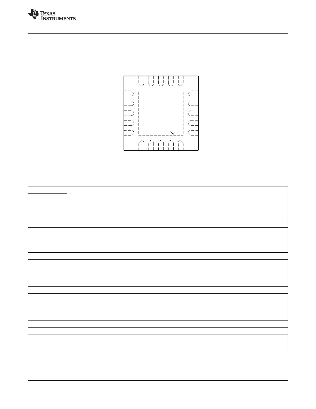
RUK PACKAGE (TOP VIEW)
PIN FUNCTIONS
PIN
NAME NO.
DRVH 14 O High-side MOSFET gate driver output.
DRVL 11 O Low-side MOSFET gate driver output.
GND 7 – Signal ground.
MODE 19 I Connect resistor to GND to configure switching frequency, control mode and discharge mode. (See Table 2)
PGND 10 – Gate driver power ground. R
PGOOD 20 O Powergood signal open drain output. PGOOD goes high when VDDQ output voltage is within the target range.
REFIN 8 I
SW 13 I/O High-side MOSFET gate driver return. R
S3 17 I S3 signal input. (See Table 1)
S5 16 I S5 signal input. (See Table 1)
TRIP 18 I Connect resistor to GND to set OCL at V
VBST 15 I High-side MOSFET gate driver bootstrap voltage input. Connect a capacitor from the VBST pin to the SW pin.
VDDQSNS 9 I VDDQ output voltage feedback. Reference input for VTTREF. Also serves as power supply for VTTREF.
VLDOIN 2 I Power supply input for VTT LDO. Connect VDDQ in typical application.
VREF 6 O 1.8-V reference output.
VTT 3 O VTT 2-A LDO output. Need to connect 10 μF or larger capacitance for stability.
VTTGND 4 – Power ground for VTT LDO.
VTTREF 5 O Buffered VTT reference output. Need to connect 0.22 μF or larger capacitance for stability.
VTTSNS 1 I VTT output voltage feedback.
V5IN 12 I 5-V power supply input for internal circuits and MOSFET gate drivers.
Thermal pad Thermal pad. Connect directly to system GND plane with multiple vias.
I/O DESCRIPTION
current sensing input(+).
DS(on)
Reference input for VDDQ. Connect to the midpoint of a resistor divider from VREF to GND. Add a capacitor for
stable operation.
current sensing input(–).
DS(on)
/8. Output 10-μA current at room temperature, TC= 4700 ppm/°C.
TRIP
Copyright © 2012, Texas Instruments Incorporated Submit Documentation Feedback 7
Product Folder Links :TPS51716
10
13
PGND
SW
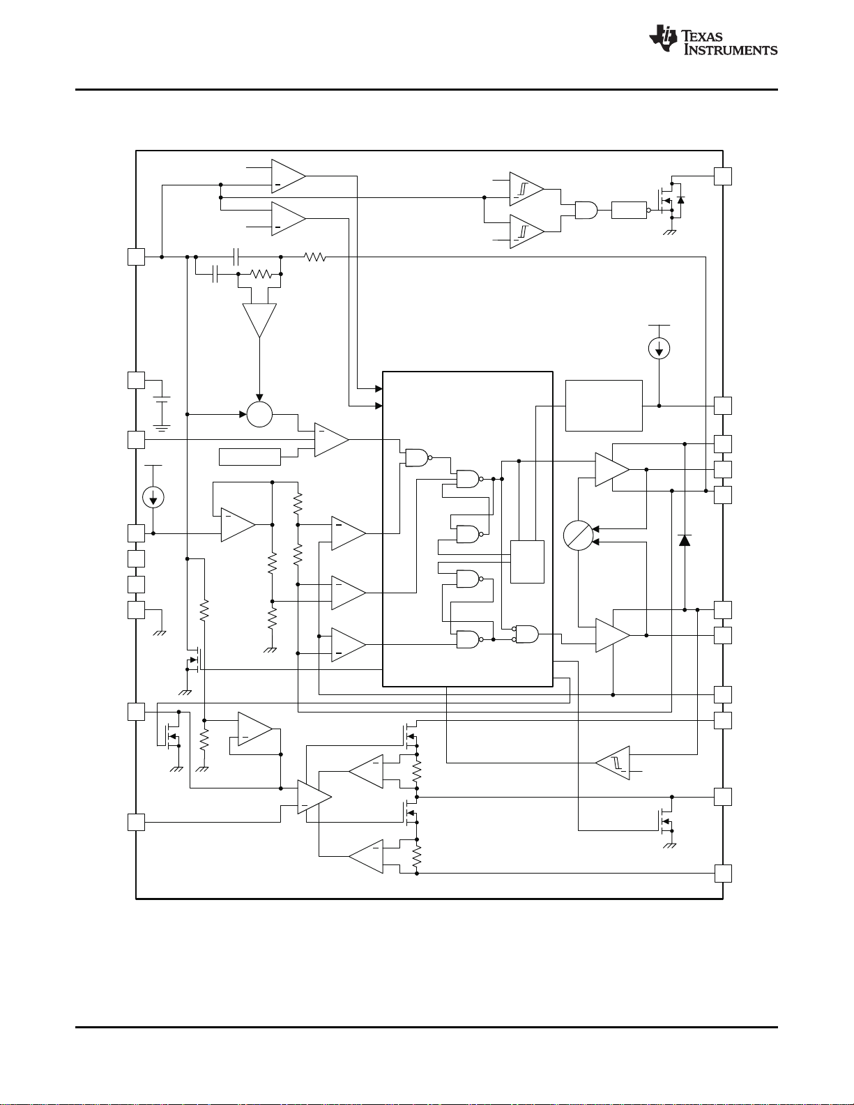
TPS517 16
OC
ZC
XCON
15
VBST
12 V5IN
PWM
9
REFIN
TRIP
Delay
20 PGOOD
Control Logic
UDG-12151
10 ?A
+
+
V
REFIN
+20%
+
+
8
VDDQSNS
+
+
18
14 DRVH
11 DRVL
t
ON
OneShot
UV
OV
V
REFIN
–32%
16S5
Soft-Start
+
NOC
+
8 R
6VREF
R
7GND
17S3
5VTTREF
1VTTSNS
4 VTTGND
3 VTT
+
+
+
+
2 VLDOIN
7 R
R
VTT Discharge
VTTREF Discharge
Mode
Selection
15 ?A
19 MODE
V
REFIN
+8/16 %
V
REFIN
–8/16 %
+
+
VDDQ
Discharge
V5OK
+
4.4 V/3.9 V
UVP
OVP
G
+
1.8 V
Σ
TPS51716
SLUSB94 –OCTOBER 2012
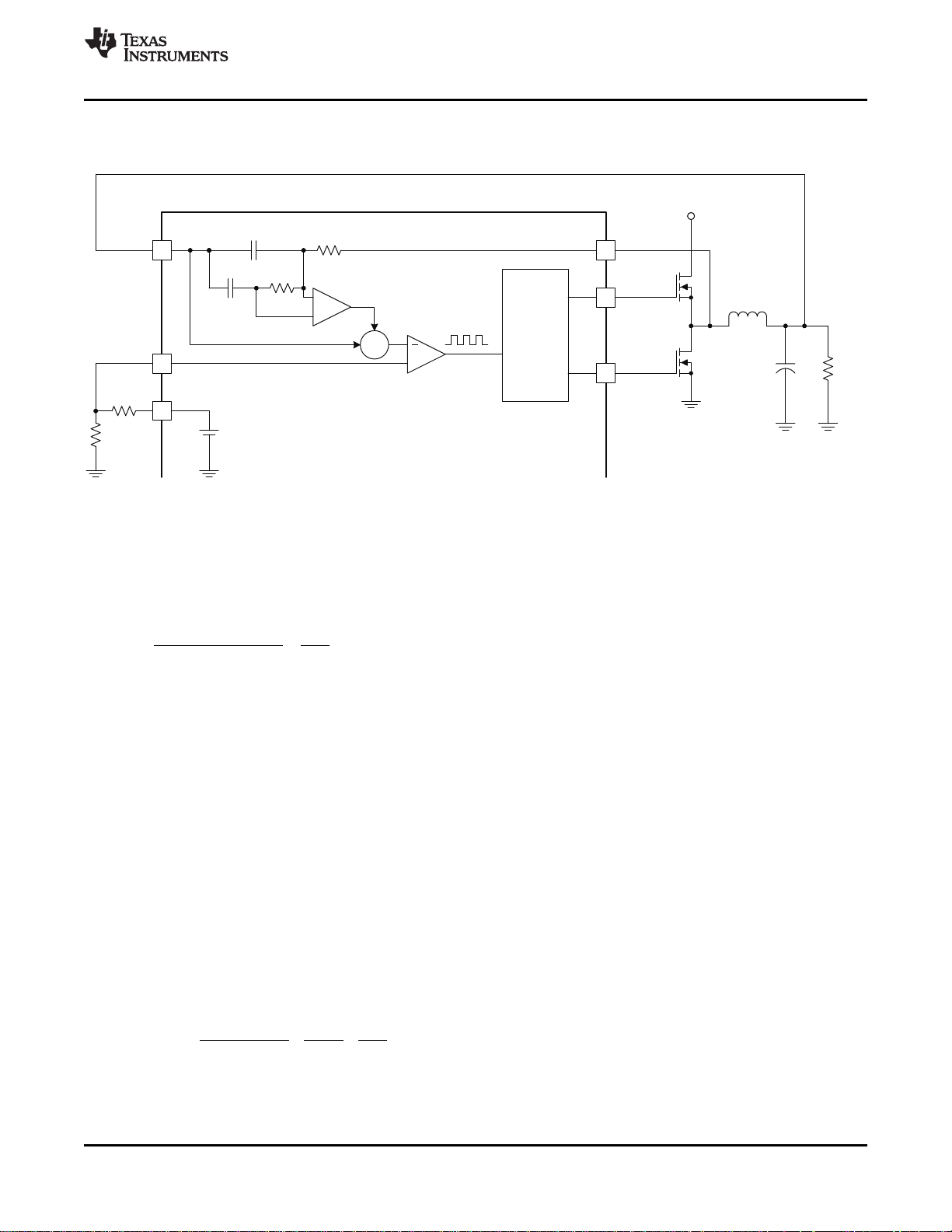
FUNCTIONAL BLOCK DIAGRAM
www.ti.com
8 Submit Documentation Feedback Copyright © 2012, Texas Instruments Incorporated
Product Folder Links :TPS51716

50
60
70
80
90
100
110
120
130
140
150
−50 −25 0 25 50 75 100 125
Junction Temperature (°C)
OVP/UVP Threshold (%)
OVP
UVP
0
3
6
9
12
15
−50 −25 0 25 50 75 100 125
Junction Temperature (°C)
VDDQSNS Discharge Current (mA)
0
2
4
6
8
10
−50 −25 0 25 50 75 100 125
Junction Temperature (°C)
VLDOIN Suppy Current (µA)
4
6
8
10
12
14
16
−50 −25 0 25 50 75 100 125
Junction Temperature (°C)
TRIP Source Current (µA)
0
200
400
600
800
1000
−50 −25 0 25 50 75 100 125
Junction Temperature (°C)
V5IN Suppy Current (µA)
0
2
4
6
8
10
−50 −25 0 25 50 75 100 125
Junction Temperature (°C)
V5IN Shutdown Current (µA)
www.ti.com
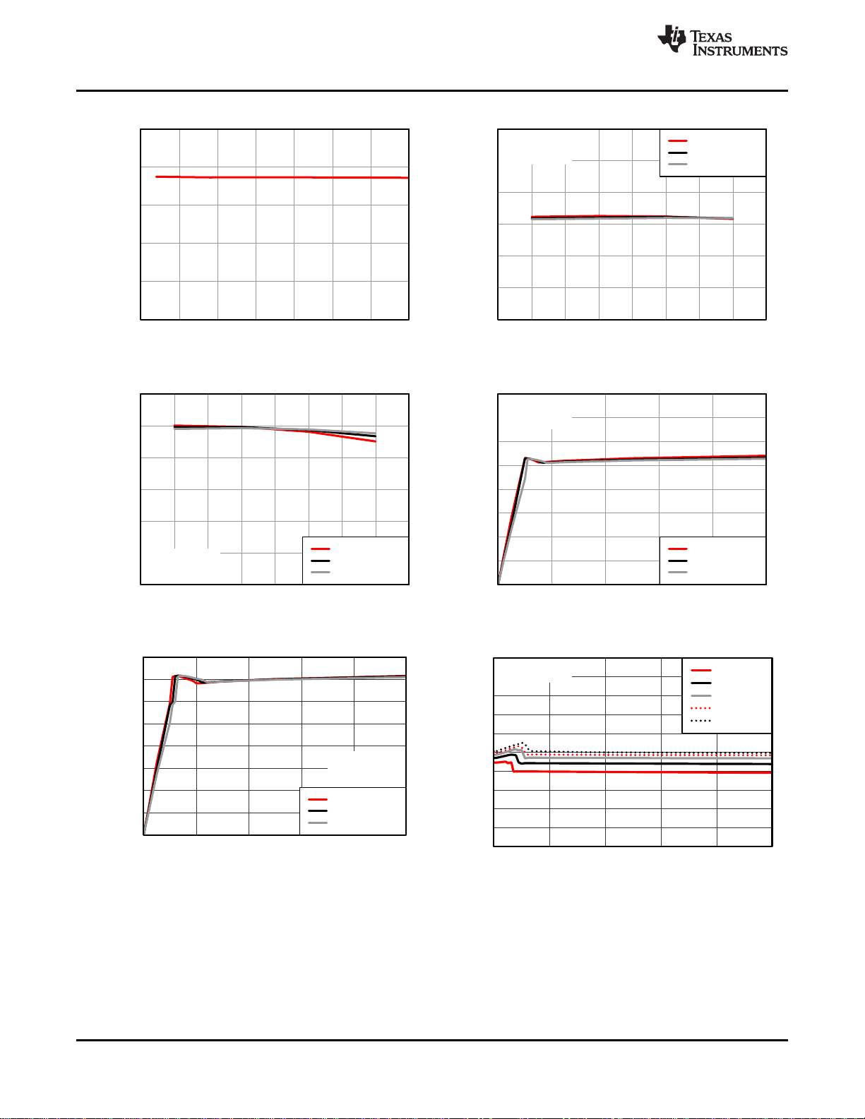
Figure 1. V5IN Supply Current vs Junction Temperature Figure 2. V5IN Shutdown Current vs Junction Temperature
TPS51716
SLUSB94 –OCTOBER 2012
TYPICAL CHARACTERISTICS
Figure 3. VLDOIN Supply Current vs Junction Temperature Figure 4. Current Sense Current vs Junction Temperature
Copyright © 2012, Texas Instruments Incorporated Submit Documentation Feedback 9
Figure 5. OVP/UVP Threshold vs Junction Temperature Figure 6. VDDQSNS Discharge Current vs Junction
Temperature
Product Folder Links :TPS51716
1.45
1.46
1.47
1.48
1.49
1.50
1.51
1.52
1.53
1.54
1.55
0 2 4 6 8 10
VDDQ Output Current (A)
VDDQ Output Voltage (V)
VIN = 3 V
VIN = 5 V
VIN = 8 V
VIN = 12 V
VIN = 20 V
R
MODE
= 1 kΩ
G000
0
100
200
300
400
500
600
700
800
0 2 4 6 8 10
VDDQ Output Current (A)
Switching Frequency (kHz)
V
VDDQ
= 1.20 V
V
VDDQ
= 1.35 V
V
VDDQ
= 1.50 V
R
MODE
= 12 kΩ
VIN = 12 V
G000
200
300
400
500
600
700
800
6 8 10 12 14 16 18 20 22
Input Voltage (V)
Switching Frequency (kHz)
V
VDDQ
= 1.20 V
V
VDDQ
= 1.35 V
V
VDDQ
= 1.50 V
R
MODE
= 12 kΩ
I
VDDQ
= 5 A
0
100
200
300
400
500
600
700
800
0 2 4 6 8 10
VDDQ Output Current (A)
Switching Frequency (kHz)
V
VDDQ
= 1.20 V
V
VDDQ
= 1.35 V
V
VDDQ
= 1.50 V
R
MODE
= 1 kΩ
VIN = 12 V
0
2
4
6
8
10
−50 −25 0 25 50 75 100 125
Junction Temperature (°C)
VTT Discharge Current (mA)
200
300
400
500
600
700
800
6 8 10 12 14 16 18 20 22
Input Voltage (V)
Switching Frequency (kHz)
V
VDDQ
= 1.20 V
V
VDDQ
= 1.35 V
V
VDDQ
= 1.50 V
R
MODE
= 1 kΩ
I
VDDQ
= 5 A
TPS51716
SLUSB94 –OCTOBER 2012
TYPICAL CHARACTERISTICS (continued)
Figure 7. VTT Discharge Current vs Junction Temperature Figure 8. Switching Frequency vs Input Voltage
www.ti.com
Figure 9. Switching Frequency vs Input Voltage Figure 10. Switching Frequency vs Load Current
10 Submit Documentation Feedback Copyright © 2012, Texas Instruments Incorporated
Figure 11. Switching Frequency vs Load Current Figure 12. Load Regulation
Product Folder Links :TPS51716

0.710
0.720
0.730
0.740
0.750
0.760
0.770
0.780
0.790
−2.0 −1.5 −1.0 −0.5 0.0 0.5 1.0 1.5 2.0
VTT Current (A)
VTT Voltage (V)
V
VDDQ
= 1.5 V
0.635
0.645
0.655
0.665
0.675
0.685
0.695
0.705
0.715
−2.0 −1.5 −1.0 −0.5 0.0 0.5 1.0 1.5 2.0
VTT Current (A)
VTT Voltage (V)
V
VDDQ
= 1.35 V
0.650
0.655
0.660
0.665
0.670
0.675
0.680
0.685
0.690
0.695
−10 −5 0 5 10
VTTREF Current (mA)
VTTREF Voltage (V)
V
VDDQ
= 1.35 V
0.580
0.585
0.590
0.595
0.600
0.605
0.610
0.615
0.620
−10 −5 0 5 10
VTTREF Current (mA)
VTTREF Voltage (V)
V
VDDQ
= 1.2 V
0.730
0.735
0.740
0.745
0.750
0.755
0.760
0.765
0.770
−10 −5 0 5 10
VTTREF Current (mA)
VTTREF Voltage (V)
V
VDDQ
= 1.5 V
1.45
1.46
1.47
1.48
1.49
1.50
1.51
1.52
1.53
1.54
1.55
2 4 6 8 10 12 14 16 18 20 22 24 26
Input Voltage (V)
VDDQ Output Voltage (V)
I
OUT
= 0 A
I
OUT
=10 A
R
MODE
= 1 kΩ
fSW = 1 kHz
G000
www.ti.com
TPS51716
SLUSB94 –OCTOBER 2012
TYPICAL CHARACTERISTICS (continued)
Figure 13. Line Regulation Figure 14. VTTREF Load Regulation
Figure 15. VTTREF Load Regulation Figure 16. VTTREF Load Regulation
Copyright © 2012, Texas Instruments Incorporated Submit Documentation Feedback 11
Figure 17. VTT Load Regulation Figure 18. VTT Load Regulation
Product Folder Links :TPS51716

0
10
20
30
40
50
60
70
80
90
100
0.001 0.01 0.1 1 10
VDDQ Output Current (A)
Efficiency (%)
VIN = 5 V
VIN = 7.4 V
VIN = 12 V
VIN = 20 V
V
VDDQ
= 1.2 V
R
MODE
= 1 kΩ
fSW = 500 kHz
L: GLMCR470A/ALPS
HS−FET: CSD17308/TI
LS−FET: CSD17309/TI
G000
0.560
0.570
0.580
0.590
0.600
0.610
0.620
0.630
0.640
−2.0 −1.5 −1.0 −0.5 0.0 0.5 1.0 1.5 2.0
VTT Current (A)
VTT Voltage (V)
V
VDDQ
= 1.2 V
0
10
20
30
40
50
60
70
80
90
100
0.001 0.01 0.1 1 10
VDDQ Output Current (A)
Efficiency (%)
VIN = 3 V
VIN = 5 V
VIN = 8 V
VIN = 12 V
VIN = 20 V
V
VDDQ
= 1.5 V
fSW = 500 kHz
G000
TPS51716
SLUSB94 –OCTOBER 2012
Figure 19. VTT Load Regulation Figure 20. Efficiency
www.ti.com
TYPICAL CHARACTERISTICS (continued)
12 Submit Documentation Feedback Copyright © 2012, Texas Instruments Incorporated
Figure 21. Efficiency
Product Folder Links :TPS51716

www.ti.com
TPS51716
SLUSB94 –OCTOBER 2012
TYPICAL CHARACTERISTICS
Figure 22. 1.5-V Startup Waveforms Figure 23. 1.5-V Startup Waveforms (0.5-V Pre-Biased)
Figure 24. 1.5-V Soft-Stop Waveforms (Tracking Discharge) Figure 25. 1.5-V Soft-Stop Waveforms (Non-Tracking
Copyright © 2012, Texas Instruments Incorporated Submit Documentation Feedback 13
Product Folder Links :TPS51716
Discharge)

10000 100000 1000000 10000000
−80
−60
−40
−20
0
20
40
60
80
−180
−135
−90
−45
0
45
90
135
180
Frequency (Hz)
Gain (dB)
Phase (°)
Gain
Phase
I
VTT
= 1 A
100 1000 10000 100000 1000000
−80
−60
−40
−20
0
20
40
60
80
−180
−135
−90
−45
0
45
90
135
180
Frequency (Hz)
Gain (dB)
Phase (°)
Gain
Phase
VIN = 12 V
I
VDDQ
= 10 A
10000 100000 1000000 10000000
−80
−60
−40
−20
0
20
40
60
80
−180
−135
−90
−45
0
45
90
135
180
Frequency (Hz)
Gain (dB)
Phase (°)
Gain
Phase
I
VTT
= −1 A
TPS51716
SLUSB94 –OCTOBER 2012
www.ti.com
TYPICAL CHARACTERISTICS
Figure 26. VDDQ Bode Plot Figure 27. VTT Bode Plot (Sink)
14 Submit Documentation Feedback Copyright © 2012, Texas Instruments Incorporated
Figure 28. VTT Bode Plot (Source)
Product Folder Links :TPS51716

700 ms400 ms 1.4 ms
S5
VREF
VDDQ
PGOOD
UDG-10137
TPS51716
www.ti.com
APPLICATION INFORMATION
VDDQ Switch Mode Power Supply Control
The TPS51716 supports D-CAP2 mode, which does not require complex external compensation networks and
are suitable for designs with small external components counts. The D-CAP2 mode is dedicated for a
configuration with very low ESR output capacitors such as multi-layer ceramic capacitors (MLCC). An adaptive
on-time control scheme is used to achieve pseudo-constant frequency. The TPS51716 adjusts the on-time (tON)
to be inversely proportional to the input voltage (VIN) and proportional to the output voltage (V
produces a switching frequency that is approximately constant over the variation of input voltage at the steady
state condition.
VREF and REFIN, VDDQ Output Voltage
The part provides a 1.8-V, ±0.8% accurate, voltage reference from VREF. This output has a 300-μA (max)
current capability to drive the REFIN input voltage through a voltage divider circuit. A capacitor with a value of
0.1-μF or larger should be attached close to the VREF terminal.
The VDDQ switch-mode power supply (SMPS) output voltage is defined by REFIN voltage, within the range
between 0.7 V and 1.8 V, programmed by the resister-divider connected between VREF and GND. (See External
Components Selection section.) A few nano farads of capacitance from REFIN to GND is recommended for
stable operation.
Soft-Start and Powergood
Provide a voltage supply to VIN and V5IN before asserting S5 to high. TPS51716 provides integrated VDDQ
soft-start functions to suppress in-rush current at start-up. The soft-start is achieved by controlling internal
reference voltage ramping up. Figure 29 shows the start-up waveforms. The switching regulator waits for 400μs
after S5 assertion. The MODE pin voltage is read in this period. A typical VDDQ ramp up duration is 700μs.
TPS51716 has a powergood open-drain output that indicates the VDDQ voltage is within the target range. The
target voltage window and transition delay times of the PGOOD comparator are ±8% (typ) and 1-ms delay for
assertion (low to high), and ±16% (typ) and 330-ns delay for de-assertion (high to low) during running. The
PGOOD start-up delay is 2.5 ms after S5 is asserted to high. Note that the time constant which is composed of
the REFIN capacitor and a resistor divider needs to be short enough to reach the target value before PGOOD
comparator enabled.
SLUSB94 –OCTOBER 2012
). This
VDDQ
Figure 29. Typical Start-up Waveforms
Copyright © 2012, Texas Instruments Incorporated Submit Documentation Feedback 15
Product Folder Links :TPS51716
TPS51716
SLUSB94 –OCTOBER 2012
Power State Control
The TPS51716 has two input pins, S3 and S5, to provide simple control scheme of power state. All of VDDQ,
VTTREF and VTT are turned on at S0 state (S3=S5=high). In S3 state (S3=low, S5=high), VDDQ and VTTREF
voltages are kept on while VTT is turned off and left at high impedance state (high-Z). The VTT output floats and
does not sink or source current in this state. In S4/S5 states (S3=S5=low), all of the three outputs are turned off
and discharged to GND according to the discharge mode selected by MODE pin. Each state code represents as
follow; S0 = full ON, S3 = suspend to RAM (STR), S4 = suspend to disk (STD), S5 = soft OFF. (See Table 1)
Table 1. S3/S5 Power State Control
STATE S3 S5 VREF VDDQ VTTREF VTT
S0 HI HI ON ON ON ON
S3 LO HI ON ON ON OFF(High-Z)
S4/S5 LO LO OFF OFF(Discharge) OFF(Discharge) OFF(Discharge)
MODE Pin Configuration
The TPS51716 reads the MODE pin voltage when the S5 signal is raised high and stores the status in a register.
A 15-μA current is sourced from the MODE pin during this time to read the voltage across the resistor connected
between the pin and GND. Table 2 shows resistor values, corresponding control mode, switching frequency and
discharge mode configurations.
Table 2. MODE Selection
MODE NO. DISCHARGE MODE
3 33 500
2 22 670
1 12 670
0 1 500
RESISTANCE BETWEEN CONTROL SWITCHING
MODE AND GND (kΩ) MODE FREQUENCY (kHz)
Non-Tracking
D-CAP2
www.ti.com
Tracking
Discharge Control
In S4/S5 state, VDDQ, VTT, and VTTREF outputs are discharged based on the respective discharge mode
selected above. The tracking discharge mode discharges VDDQ output through the internal VTT regulator
transistors enabling quick 13 ms discharge operation. The VTT output maintains tracking of the VTTREF voltage
in this mode. (Please refer to Figure 24) After 4 ms of tracking discharge operation, the mode changes to nontracking discharge. The VDDQ output must be connected to the VLDOIN pin in this mode. The non-tracking
mode discharges the VDDQ and VTT pins using internal MOSFETs that are connected to corresponding output
terminals. The non-tracking discharge is slow compared with the tracking discharge due to the lower current
capability of these MOSFETs. (Please refer to Figure 25)
16 Submit Documentation Feedback Copyright © 2012, Texas Instruments Incorporated
Product Folder Links :TPS51716
( )
-
= ´ ´
´
IN OUT
OUT
LOAD(LL)
X IN SW
V V
V
1
I
2 L V f
´
= £
p´ ´ ´
C C SW
0
X OUT
R C f
f
2 G L C 3
Control
Logic
and
Driver
L
X
C
OUTRLOAD
UDG-12150
9
C
C1
V
IN
14
13
11
SW
DRVH
DRVL
VDDQSNS
G
8
REFIN
6
VREF
+
1.8 V
R
C1
C
C2
R
C2
R1
R2
TPS51716
VDDQ
Σ
+
PWM
www.ti.com
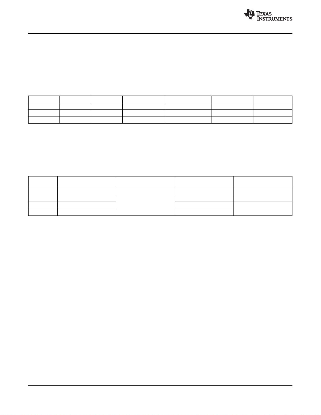
D-CAP2 Mode Operation
Figure 30 shows simplified model of D-CAP2 architecture.
Figure 30. Simplified Modulator Using D-CAP2 Mode
TPS51716
SLUSB94 –OCTOBER 2012
The D-CAP2 mode in the TPS51716 includes an internal feedback network enabling the use of very low ESR
output capacitor(s) such as multi-layer ceramic capacitors. The role of the internal network is to sense the ripple
component of the inductor current information and combine it with voltage feedback signal. Using RC1=RC2≡R
and CC1=CC2≡CC, 0-dB frequency of the D-CAP2 mode is given by Equation 1. It is recommended that the 0-dB
frequency (f0) be lower than 1/3 of the switching frequency to secure the proper phase margin
where
The typical G value is 0.25, and typical RCCCtime constant values for 500 kHz and 670 kHz operation are 23 µs
and 14.6 µs, respectively.
For example, when fSW=500 kHz and LX=1 µH, C
When selecting the capacitor, pay attention to its characteristics. For MLCC use X5R or better dielectric and
consider the derating of the capacitance by both DC bias and AC bias. When derating by DC bias and AC bias
are 80% and 50%, respectively, the effective derating is 40% because 0.8 x 0.5 = 0.4. The capacitance of
specialty polymer capacitors may change depending on the operating frequency. Consult capacitor
manufacturers for specific characteristics.
Light-Load Operation
In auto-skip mode, the TPS51716 SMPS control logic automatically reduces its switching frequency to improve
light-load efficiency. To achieve this intelligence, a zero cross detection comparator is used to prevent negative
inductor current by turning off the low-side MOSFET. Equation 2 shows the boundary load condition of this skip
mode and continuous conduction operation.
Copyright © 2012, Texas Instruments Incorporated Submit Documentation Feedback 17
• G is gain of the amplifier which amplifies the ripple current information generated by the compensation
circuit (1)
should be larger than 88 µF.
OUT
Product Folder Links :TPS51716
C
(2)
12
17
16
6
15
14
13
11
V5IN
TPS51716
S3
S5
VREF
VBST
DRVH
SW
DRVL
8
10
REFIN
PGND
7
19
GND
MODE
18 TRIP
20
9
2
3
PGOOD
VDDQSNS
VLDOIN
VTT
1
4
5
VTTSNS
VTTGND
VTTREF
UDG-12152
VDDQ
S5
PGND
5VIN
PGND
VIN
AGND
Powergood
PGND
1 kW
PGND
PGND
0.22 mF
AGND
TPS51716
SLUSB94 –OCTOBER 2012
VTT and VTTREF
TPS51716 integrates two high performance, low-drop-out linear regulators, VTT and VTTREF, to provide
complete DDR2/DDR3/DDR3L/LPDDR3 power solutions. The VTTREF has a 10-mA sink/source current
capability, and tracks ½ of VDDQSNS with ±1% accuracy using an on-chip ½ divider. A 0.22-μF (or larger)
ceramic capacitor must be connected close to the VTTREF terminal to ensure stable operation. The VTT
responds quickly to track VTTREF within ±40 mV at all conditions, and the current capability is 2 A for both sink
and source. A 10-μF (or larger) ceramic capacitor(s) need to be connected close to the VTT terminal for stable
operation. To achieve tight regulation with minimum effect of wiring resistance, a remote sensing terminal,
VTTSNS, should be connected to the positive node of VTT output capacitor(s) as a separate trace from the highcurrent line to the VTT pin. (Please refer to the Layout Considerations section for details.)
When VTT is not required in the design, following treatment is strongly recommended.
• Connect VLDOIN to VDDQ.
• Tie VTTSNS to VTT, and remove capacitors from VTT to float.
• Connect VTTGND to GND.
• Select MODE2, 3, 4 or 5 shown in Table 2 (Select Non-tracking discharge mode).
• Maintain a 0.22-µF capacitor connected at VTTREF.
• Pull down S3 to GND with 1-kΩ resistance.
www.ti.com
Figure 31. Application Circuit When VTT Is Not Required
VDDQ Overvoltage and Undervoltage Protection
The TPS51716 sets the overvoltage protection (OVP) when VDDQSNS voltage reaches a level 20% (typ) higher
than the REFIN voltage. When an OV event is detected, the controller changes the output target voltage to 0 V.
This usually turns off DRVH and forces DRVL to be on. When the inductor current begins to flow through the
low-side MOSFET and reaches the negative OCL, DRVL is turned off and DRVH is turned on, for a minimum ontime.
After the minimum on-time expires, DRVH is turned off and DRVL is turned on again. This action minimizes the
output node undershoot due to LC resonance. When the VDDQSNS reaches 0 V, the driver output is latched as
DRVH off, DRVL on. VTTREF and VTT are turned off and discharged using the non-tracking discharge
MOSFETs regardless of the tracking mode.
18 Submit Documentation Feedback Copyright © 2012, Texas Instruments Incorporated
Product Folder Links :TPS51716

( ) ( )
æ ö æ ö
-
ç ÷ ç ÷
= + = + ´ ´
ç ÷ ç ÷
´
è ø è ø
IND(ripple)
OCTRIP OCTRIP IN OUT OUT
OCL
X SW IN
DS on DS on
I
V V V V V
1
I
R 2 R 2 L f V
= ´
TRIP
OCTRIP TRIP
I
V R
8
TPS51716
www.ti.com
The undervoltage protection (UVP) latch is set when the VDDQSNS voltage remains lower than 68% (typ) of the
REFIN voltage for 1 ms or longer. In this fault condition, the controller latches DRVH low and DRVL low and
discharges the VDDQ, VTT and VTTREF outputs. UVP detection function is enabled after 1.2 ms of SMPS
operation to ensure startup.
To release the OVP and UVP latches, toggle S5 or adjust the V5IN voltage down and up beyond the
undervoltage lockout threshold.
VDDQ Out-of-Bound Operation
When the output voltage rises to 8% above the target value, the out-of-bound operation starts. During the out-ofbound condition, the controller operates in forced PWM-only mode. Turning on the low-side MOSFET beyond the
zero inductor current quickly discharges the output capacitor. During this operation, the cycle-by-cycle negative
overcurrent limit is also valid. Once the output voltage returns to within regulation range, the controller resumes
to auto-skip mode.
VDDQ Overcurrent Protection
The VDDQ SMPS has cycle-by-cycle overcurrent limiting protection. The inductor current is monitored during the
off-state using the low-side MOSFET R
is larger than the overcurrent trip level. The current monitor circuit inputs are PGND and SW pins so that those
should be properly connected to the source and drain terminals of low-side MOSFET. The overcurrent trip level,
V
and GND, and I
, is determined by Equation 3, where R
OCTRIP
is the current sourced from the TRIP pin. I
TRIP
has 4700ppm/°C temperature coefficient to compensate the temperature dependency of the low-side MOSFET
R
DS(on)
.
, and the controller maintains the off-state when the inductor current
DS(on)
is the value of the resistor connected between the TRIP pin
TRIP
is 10 μA typically at room temperature, and
TRIP
SLUSB94 –OCTOBER 2012
(3)
Because the comparison is done during the off-state, V
load current OCL level, I
, can be calculated by considering the inductor ripple current as shown in Equation 4.
OCL
OCTRIP
sets the valley level of the inductor current. The
where
• I
IND(ripple)
is inductor ripple current (4)
In an overcurrent condition, the current to the load exceeds the current to the output capacitor, thus the output
voltage tends to fall down. Eventually, it crosses the undervoltage protection threshold and shuts down.
VTT Overcurrent Protection
The LDO has an internally fixed constant overcurrent limiting of 3-A (typ) for both sink and source operation.
V5IN Undervoltage Lockout Protection
The TPS51716 has a 5-V supply undervoltage lockout protection (UVLO) threshold. When the V5IN voltage is
lower than UVLO threshold voltage, typically 3.9 V, VDDQ, VTT and VTTREF are shut off. This is a non-latch
protection.
Thermal Shutdown
The TPS51716 includes an internal temperature monitor. If the temperature exceeds the threshold value, 140°C
(typ), VDDQ, VTT and VTTREF are shut off. The state of VDDQ is open, and that of VTT and VTTREF are high
impedance (high-Z) at thermal shutdown. The discharge functions of all outputs are disabled. This is a non-latch
protection and the operation is restarted with soft-start sequence when the device temperature is reduced by
10°C (typ).
Copyright © 2012, Texas Instruments Incorporated Submit Documentation Feedback 19
Product Folder Links :TPS51716
( )
( )
( )
æ ö
æ ö
-
ç ÷
´ - ´ ´
ç ÷
ç ÷
ç ÷
´
´
è ø
è ø
=
IN OUT
OUT
OCL DS(on)
X
SW IN
TRIP
TRIP
V V
V
8 I R
2 L
f V
R
I
( )
( )
( )
(
)
( )
- ´
´
= + ´
´ ´
IN OUT OUT
max
TRIP TRIP
IND peak
SW IN
DS on max
V V V
R I
1
I
8 R L f V
( )
( )
(
)
( ) ( )
( )
(
)
( )
- ´ - ´
= ´ = ´
´ ´
IN OUT OUT IN OUT OUT
max max
X
SW IN O SW IN
IND ripple max max max
V V V V V V
1 3
L
I f V I f V
IND(ripple)
OUT(ripple)
OUT SW
I
V
8 C f
=
´ ´
OUT(ripple) IND(ripple)
V I ESR= ´
OUT(ripple)
OUT
R1
R2
1.8
1
V
V
2
=
æ ö
ç ÷
ç ÷
-
ç ÷
-
ç ÷
è ø
TPS51716
SLUSB94 –OCTOBER 2012
External Components Selection
The external components selection is a simple process.
1. DETERMINE THE VALUE OF R1 AND R2
The output voltage is determined by the value of the voltage-divider resistor, R1 and R2. R1 is connected
between VREF and REFIN pins, and R2 is connected between the REFIN pin and GND. Setting R1 to 10-kΩ is a
good starting point. Determine R2 using Equation 5.
For an application using organic semiconductor capacitor(s) or specialty polymer capacitor(s) for the output
capacitor(s), the output voltage ripple can be calculated as shown in Equation 6.
For an application using ceramic capacitor(s) as the output capacitor(s), the output voltage ripple can be
calculated as shown in Equation 7.
www.ti.com
(5)
(6)
(7)
2. CHOOSE THE INDUCTOR
The inductance value should be determined to yield a ripple current of approximately ¼ to ½ of maximum output
current. Larger ripple current increases output ripple voltage and improves the signal-to-noise ratio and helps
stable operation.
(8)
The inductor needs a low direct current resistance (DCR) to achieve good efficiency, as well as enough room
above peak inductor current before saturation. The peak inductor current can be estimated in Equation 9.
(9)
3. CHOOSE THE OCL SETTING RESISTANCE, R
Combining Equation 3 and Equation 4, R
TRIP
TRIP
can be obtained using Equation 10.
(10)
20 Submit Documentation Feedback Copyright © 2012, Texas Instruments Incorporated
Product Folder Links :TPS51716
1
2
3
4
15
14
13
12
VTTSNS
U1
TPS51716RUK
VLDOIN
VTT
VTTGND
VBST
DRVH
SW
V5IN
5 11VTTREF DRVL
10987
PGND
VDDQSNS
REFIN
GND
6
VREF
16171819
S5
S3
TRIP
MODE
20
PGOOD
21
PwPad
C6
1 mF
UDG-12148
C7
0.1 mFC810 mFC910 mF
V
IN
8 V to 20 V
PGND
R6
0 W
C5
0.1 mF
R7 0 W
L1
1 mH
Q2
FDMS8670AS
(1)
C10
4 x 47 mF
VDDQ_GND
PGND
R5
49.9 kW
R4
10 kW
C3
0.1 mF
C4
10 nF
C2
0.22 mF
C1
10 mF
C12
10 mF
PGND
VTT
0.75 V/2 A
VTTREF
0.75 V
VTTGND
S5
S3
R1
100 kW
R2 1 kW
R3 36 kW
V5IN
4.5 V to 5.5 V
Q1
FDMS8680
(1)
VDDQ
1.5 V/10 A
AGND
PGND
AGND
PGND
´
£
p´ ´ ´
C C SW
X OUT
R C f
2 G L C 3
www.ti.com
4. CHOOSE THE OUTPUT CAPACITORS
Determine output capacitance to meet small signal stability as shown in Equation 11.
where
• RC×CCtime constant is 23 µs for 500 kHz operation (or 14.6 µs for 670 kHz operation)
• G = 0.25 (11)
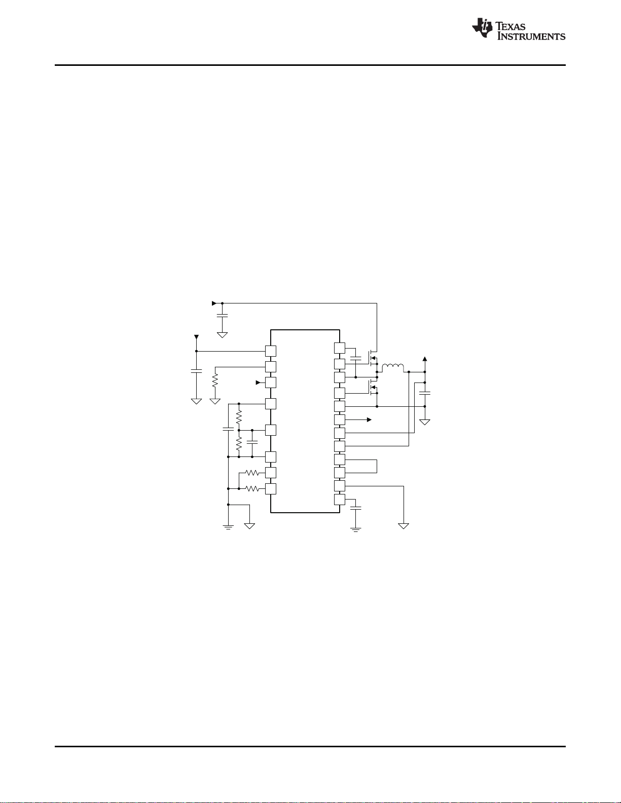
TPS51716 Application Circuits
TPS51716
SLUSB94 –OCTOBER 2012
(1) TI NexFET™ power MOSFETs are available and can be used in this application. Please contact your local TI
representative.
REFERENCE
DESIGNATOR
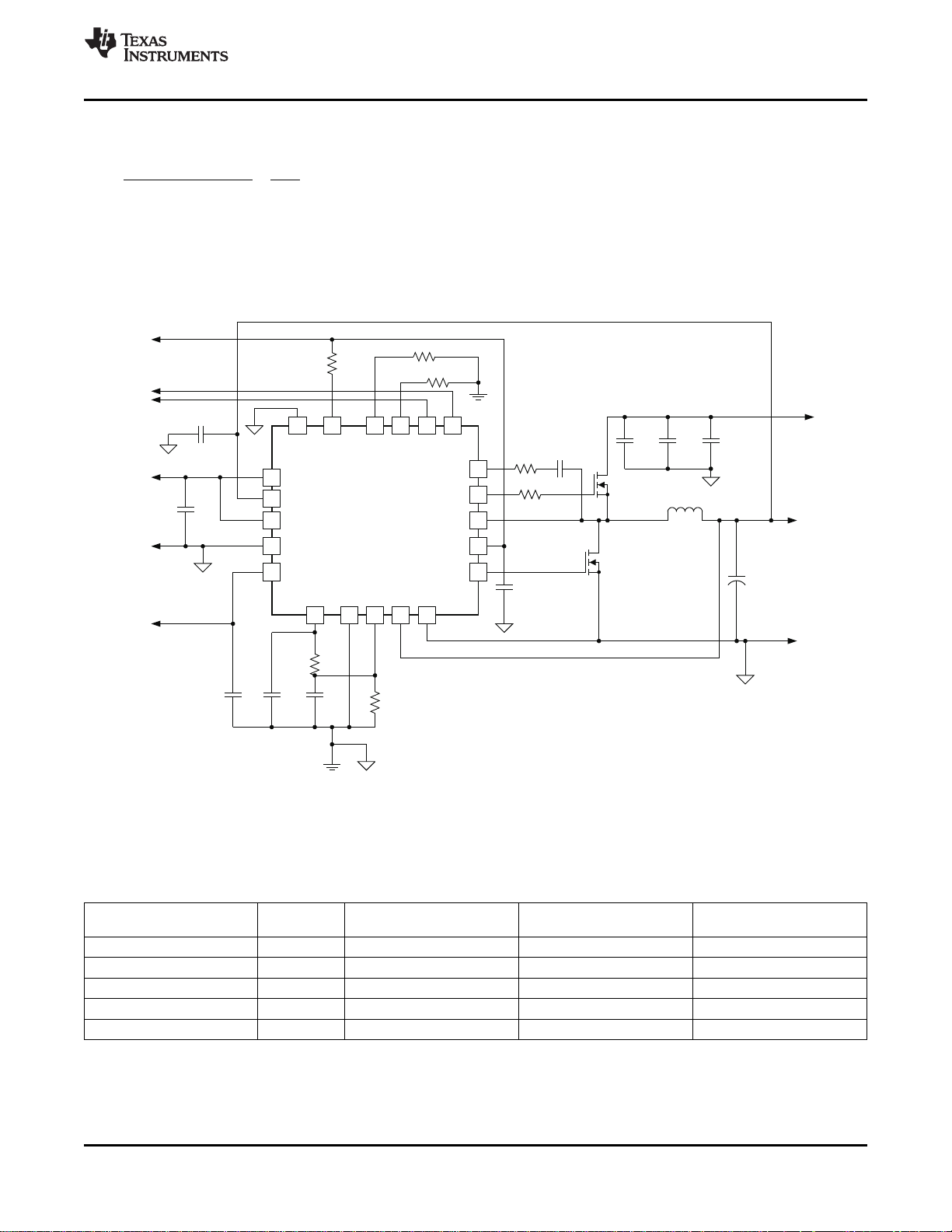
C8, C9 2 10 µF, 25 V Taiyo Yuden TMK325BJ106MM
C10 4 47 µF, 6.3 V TDK C2012X5R0J476M
L1 1 1 µH, 18.5 A, 2.3 mΩ NEC Tokin MPC1055L1R0C
Q1 1 30 V, 35 A, 8.5 mΩ Fairchild FDMS8680
Q2 1 30 V, 42 A, 3.5 mΩ Fairchild FDMS8670AS
Copyright © 2012, Texas Instruments Incorporated Submit Documentation Feedback 21
Figure 32. DDR3, DCAP-2 500-kHz Application Circuit, Tracking Discharge
Table 3. DDR3, DCAP-2 500-kHz Application Circuit, List of Materials
QTY SPECIFICATION MANUFACTURE PART NUMBER
Product Folder Links :TPS51716

TPS51716
DRVL
11
VIN
REFIN GND
V5IN
12
V
OUT
TRIP
MODE
10
7
PGND
VREF
19
18
4
3
VTT
UDG-12149
VTTGND
5
0.22 ?F
VTTREF
2
86
10 ?F
10 nF
0.1 ?F
VTT
VTTGND
VLDOIN
1 ?F
#1
#2
#3
PGND
AGND
TPS51716
SLUSB94 –OCTOBER 2012
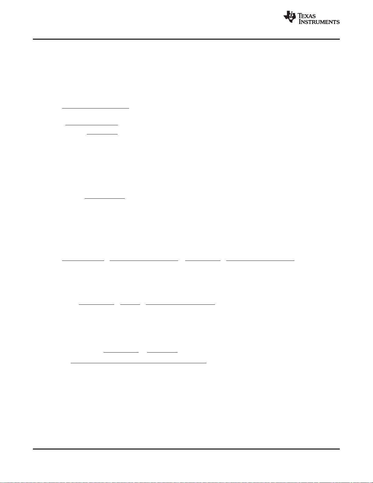
Layout Considerations
Certain issues must be considered before designing a layout using the TPS51716.
www.ti.com
Figure 33. DC/DC Converter Ground System
• VIN capacitor(s), VOUT capacitor(s) and MOSFETs are the power components and should be placed on one
side of the PCB (solder side). Other small signal components should be placed on another side (component
side). At least one inner system GND plane should be inserted, in order to shield and isolate the small signal
traces from noisy power lines.
• All sensitive analog traces and components such as VDDQSNS, VTTSNS, MODE, REFIN, VREF and TRIP
should be placed away from high-voltage switching nodes such as SW, DRVL, DRVH or VBST to avoid
coupling. Use internal layer(s) as system GND plane(s) and shield feedback trace from power traces and
components.
• The DC/DC converter has several high-current loops. The area of these loops should be minimized in order to
suppress generating switching noise.
– The most important loop to minimize the area of is the path from the VIN capacitor(s) through the high and
low-side MOSFETs, and back to the negative node of the VIN capacitor(s). Connect the negative node of
the VIN capacitor(s) and the source of the low-side MOSFET as close as possible. (Refer to loop #1 of
Figure 33)
– The second important loop is the path from the low-side MOSFET through inductor and VOUT
capacitor(s), and back to source of the low-side MOSFET. Connect the source of the low-side MOSFET
and negative node of VOUT capacitor(s) as close as possible. (Refer to loop #2 of Figure 33)
– The third important loop is of gate driving system for the low-side MOSFET. To turn on the low-side
MOSFET, high current flows from V5IN capacitor through gate driver and the low-side MOSFET, and back
to negative node of the capacitor. To turn off the low-side MOSFET, high current flows from gate of the
low-side MOSFET through the gate driver and PGND pin, and back to source of the low-side MOSFET.
Connect negative node of V5IN capacitor, source of the low-side MOSFET and PGND pin as close as
possible. (Refer to loop #3 of Figure 33)
• Connect negative nodes of the VTTREF output capacitor, VREF capacitor and REFIN capacitor and bottomside resistance of VREF voltage-divider to GND pin as close as possible. The negative node of the VTT
22 Submit Documentation Feedback Copyright © 2012, Texas Instruments Incorporated
Product Folder Links :TPS51716

TPS51716
www.ti.com
output capacitor(s), VTTGND, GND and PGND pins should be connected to system GND plane near the
device as shown in Figure 33.
• Because the TPS51716 controls output voltage referring to voltage across VOUT capacitor, VDDQSNS
should be connected to the positive node of VOUT capacitor using different trace from that for VLDOIN.
Remember that this sensing potential is the reference voltage of VTTREF. Avoid any noise generative lines.
GND pin refers to the negative node of VOUT capacitor.
• Connect the overcurrent setting resistor from TRIP pin to GND pin and make the connections as close as
possible to the device to avoid coupling from a high-voltage switching node.
• Connect the frequency and mode setting resistor from MODE pin to GND pin ground, and make the
connections as close as possible to the device to avoid coupling from a high-voltage switching node.
• Connections from gate drivers to the respective gate of the high-side or the low-side MOSFET should be as
short as possible to reduce stray inductance. Use 0.65 mm (25 mils) or wider trace and via(s) of at least 0.5
mm (20 mils) diameter along this trace.
• The PCB trace defined as SW node, which connects to the source of the high-side MOSFET, the drain of the
low-side MOSFET and the high-voltage side of the inductor, should be as short and wide as possible.
• VLDOIN should be connected to VOUT with short and wide traces. An input bypass capacitor should be
placed as close as possible to the pin with short and wide connections. The negative node of the capacitor
should be connected to system GND plane.
• The output capacitor for VTT should be placed close to the pins with a short and wide connection in order to
avoid additional ESR and/or ESL of the trace.
• VTTSNS should be connected to the positive node of the VTT output capacitor(s) using a separate trace from
the high-current power line. When remote sensing is required attach the output capacitor(s) at that point.
Also, it is recommended to minimize any additional ESR and/or ESL of ground trace between GND pin and
the output capacitor(s).
• Consider adding a low pass filter (LPF) at VTTSNS in case the ESR of the VTT output capacitor(s) is larger
than 2 mΩ.
• In order to effectively remove heat from the package, prepare a thermal land and solder to the package
thermal pad. Wide trace of the component-side copper, connected to this thermal land, helps heat spreading.
Numerous vias with a 0.3-mm diameter connected from the thermal land to the internal/solder-side ground
plane(s) should be used to help dissipation. The thermal land can be connected to either AGND or PGND but
is recommended to be connected to PGND, the system GND plane(s), which has better heat radiation.
SLUSB94 –OCTOBER 2012
Copyright © 2012, Texas Instruments Incorporated Submit Documentation Feedback 23
Product Folder Links :TPS51716
PACKAGE OPTION ADDENDUM
www.ti.com
10-Dec-2012
PACKAGING INFORMATION
Orderable Device Status
TPS51716RUKR ACTIVE WQFN RUK 20 3000 Green (RoHS
TPS51716RUKT ACTIVE WQFN RUK 20 250 Green (RoHS
(1)
The marketing status values are defined as follows:
ACTIVE: Product device recommended for new designs.
LIFEBUY: TI has announced that the device will be discontinued, and a lifetime-buy period is in effect.
NRND: Not recommended for new designs. Device is in production to support existing customers, but TI does not recommend using this part in a new design.
PREVIEW: Device has been announced but is not in production. Samples may or may not be available.
OBSOLETE: TI has discontinued the production of the device.
Package Type Package
(1)
Drawing
Pins Package Qty Eco Plan
(2)
& no Sb/Br)
& no Sb/Br)
Lead/Ball Finish MSL Peak Temp
(3)
CU NIPDAU Level-2-260C-1 YEAR
CU NIPDAU Level-2-260C-1 YEAR
Samples
(Requires Login)
(2)
Eco Plan - The planned eco-friendly classification: Pb-Free (RoHS), Pb-Free (RoHS Exempt), or Green (RoHS & no Sb/Br) - please check http://www.ti.com/productcontent for the latest availability
information and additional product content details.
TBD: The Pb-Free/Green conversion plan has not been defined.
Pb-Free (RoHS): TI's terms "Lead-Free" or "Pb-Free" mean semiconductor products that are compatible with the current RoHS requirements for all 6 substances, including the requirement that
lead not exceed 0.1% by weight in homogeneous materials. Where designed to be soldered at high temperatures, TI Pb-Free products are suitable for use in specified lead-free processes.
Pb-Free (RoHS Exempt): This component has a RoHS exemption for either 1) lead-based flip-chip solder bumps used between the die and package, or 2) lead-based die adhesive used between
the die and leadframe. The component is otherwise considered Pb-Free (RoHS compatible) as defined above.
Green (RoHS & no Sb/Br): TI defines "Green" to mean Pb-Free (RoHS compatible), and free of Bromine (Br) and Antimony (Sb) based flame retardants (Br or Sb do not exceed 0.1% by weight
in homogeneous material)
(3)
MSL, Peak Temp. -- The Moisture Sensitivity Level rating according to the JEDEC industry standard classifications, and peak solder temperature.
Important Information and Disclaimer:The information provided on this page represents TI's knowledge and belief as of the date that it is provided. TI bases its knowledge and belief on information
provided by third parties, and makes no representation or warranty as to the accuracy of such information. Efforts are underway to better integrate information from third parties. TI has taken and
continues to take reasonable steps to provide representative and accurate information but may not have conducted destructive testing or chemical analysis on incoming materials and chemicals.
TI and TI suppliers consider certain information to be proprietary, and thus CAS numbers and other limited information may not be available for release.
In no event shall TI's liability arising out of such information exceed the total purchase price of the TI part(s) at issue in this document sold by TI to Customer on an annual basis.
Addendum-Page 1
PACKAGE MATERIALS INFORMATION
www.ti.com 7-Dec-2012
TAPE AND REEL INFORMATION
*All dimensions are nominal
Device Package
TPS51716RUKR WQFN RUK 20 3000 330.0 12.4 3.3 3.3 1.1 8.0 12.0 Q2
TPS51716RUKT WQFN RUK 20 250 180.0 12.4 3.3 3.3 1.1 8.0 12.0 Q2
Type
Package
Drawing
Pins SPQ Reel
Diameter
(mm)
Reel
Width
W1 (mm)
A0
(mm)B0(mm)K0(mm)P1(mm)W(mm)
Pin1
Quadrant
Pack Materials-Page 1

PACKAGE MATERIALS INFORMATION
www.ti.com 7-Dec-2012
*All dimensions are nominal
Device Package Type Package Drawing Pins SPQ Length (mm) Width (mm) Height (mm)
TPS51716RUKR WQFN RUK 20 3000 367.0 367.0 35.0
TPS51716RUKT WQFN RUK 20 250 210.0 185.0 35.0
Pack Materials-Page 2


IMPORTANT NOTICE
Texas Instruments Incorporated and its subsidiaries (TI) reserve the right to make corrections, enhancements, improvements and other
changes to its semiconductor products and services per JESD46, latest issue, and to discontinue any product or service per JESD48, latest
issue. Buyers should obtain the latest relevant information before placing orders and should verify that such information is current and
complete. All semiconductor products (also referred to herein as “components”) are sold subject to TI’s terms and conditions of sale
supplied at the time of order acknowledgment.
TI warrants performance of its components to the specifications applicable at the time of sale, in accordance with the warranty in TI’s terms
and conditions of sale of semiconductor products. Testing and other quality control techniques are used to the extent TI deems necessary
to support this warranty. Except where mandated by applicable law, testing of all parameters of each component is not necessarily
performed.
TI assumes no liability for applications assistance or the design of Buyers’ products. Buyers are responsible for their products and
applications using TI components. To minimize the risks associated with Buyers’ products and applications, Buyers should provide
adequate design and operating safeguards.
TI does not warrant or represent that any license, either express or implied, is granted under any patent right, copyright, mask work right, or
other intellectual property right relating to any combination, machine, or process in which TI components or services are used. Information
published by TI regarding third-party products or services does not constitute a license to use such products or services or a warranty or
endorsement thereof. Use of such information may require a license from a third party under the patents or other intellectual property of the
third party, or a license from TI under the patents or other intellectual property of TI.
Reproduction of significant portions of TI information in TI data books or data sheets is permissible only if reproduction is without alteration
and is accompanied by all associated warranties, conditions, limitations, and notices. TI is not responsible or liable for such altered
documentation. Information of third parties may be subject to additional restrictions.
Resale of TI components or services with statements different from or beyond the parameters stated by TI for that component or service
voids all express and any implied warranties for the associated TI component or service and is an unfair and deceptive business practice.
TI is not responsible or liable for any such statements.
Buyer acknowledges and agrees that it is solely responsible for compliance with all legal, regulatory and safety-related requirements
concerning its products, and any use of TI components in its applications, notwithstanding any applications-related information or support
that may be provided by TI. Buyer represents and agrees that it has all the necessary expertise to create and implement safeguards which
anticipate dangerous consequences of failures, monitor failures and their consequences, lessen the likelihood of failures that might cause
harm and take appropriate remedial actions. Buyer will fully indemnify TI and its representatives against any damages arising out of the use
of any TI components in safety-critical applications.
In some cases, TI components may be promoted specifically to facilitate safety-related applications. With such components, TI’s goal is to
help enable customers to design and create their own end-product solutions that meet applicable functional safety standards and
requirements. Nonetheless, such components are subject to these terms.
No TI components are authorized for use in FDA Class III (or similar life-critical medical equipment) unless authorized officers of the parties
have executed a special agreement specifically governing such use.
Only those TI components which TI has specifically designated as military grade or “enhanced plastic” are designed and intended for use in
military/aerospace applications or environments. Buyer acknowledges and agrees that any military or aerospace use of TI components
which have not been so designated is solely at the Buyer's risk, and that Buyer is solely responsible for compliance with all legal and
regulatory requirements in connection with such use.
TI has specifically designated certain components as meeting ISO/TS16949 requirements, mainly for automotive use. In any case of use of
non-designated products, TI will not be responsible for any failure to meet ISO/TS16949.
Products Applications
Audio www.ti.com/audio Automotive and Transportation www.ti.com/automotive
Amplifiers amplifier.ti.com Communications and Telecom www.ti.com/communications
Data Converters dataconverter.ti.com Computers and Peripherals www.ti.com/computers
DLP® Products www.dlp.com Consumer Electronics www.ti.com/consumer-apps
DSP dsp.ti.com Energy and Lighting www.ti.com/energy
Clocks and Timers www.ti.com/clocks Industrial www.ti.com/industrial
Interface interface.ti.com Medical www.ti.com/medical
Logic logic.ti.com Security www.ti.com/security
Power Mgmt power.ti.com Space, Avionics and Defense www.ti.com/space-avionics-defense
Microcontrollers microcontroller.ti.com Video and Imaging www.ti.com/video
RFID www.ti-rfid.com
OMAP Applications Processors www.ti.com/omap TI E2E Community e2e.ti.com
Wireless Connectivity www.ti.com/wirelessconnectivity
Mailing Address: Texas Instruments, Post Office Box 655303, Dallas, Texas 75265
Copyright © 2012, Texas Instruments Incorporated

 Loading...