

Page 1
TPS51427
TPS51427
www.ti.com
................................................................................................................................................ SLUS819B – APRIL 2008 – REVISED SEPTEMBER 2008
DUAL D-CAP™ SYNCHRONOUS STEP-DOWN CONTROLLER
FOR NOTEBOOK POWER RAILS
1
FEATURES
23
• Fixed-Frequency Emulated On-Time Control;
Frequency Selectable from Three Options
• D-CAP™ Mode Enables Fast Transient
Response Less than 100 ns
• Advanced Ramp Compensation Allows Low
Output Ripple with Minimal Jitter
• Selectable PWM-Only/ OOA™/Auto-Skip Modes
• Wide Input Voltage Range: 5.5 V to 28 V
• Dual Fixed or Adjustable SMPS:
– 0.7 V to 5.9 V (Channel1)
– 0.5 V to 2.5 V (Channel2)
• Fixed 3.3-V/5-V, or Adjustable Output 0.7-V to
4.5-V LDO; Capable of Sourcing 100 mA
• Fixed 3.3-VREF Output Capable of Sourcing
10 mA
• Temperature Compensated Low-Side R
Current Sensing
• Adaptive Gate Drivers with Integrated Boost
Switch
• Bootstrap Charge Auto Refresh
• Integrated Soft Start, Tracking Soft Stop
• Independent PGOOD and EN for Each Channel
APPLICATIONS
• Notebook I/O and System Bus Rails
• Graphics Application
• PDAs and Mobile Communication Devices
DS(on)
DESCRIPTION
The TPS51427 is a dual synchronous step-down
controller designed for notebook and mobile
communications applications. This device is part of a
low-cost suite of notebook power bus regulators that
enables system designs with low external component
counts. The TPS51427 includes two
pulse-width-modulation (PWM) controllers, SMPS1
and SMPS2. The output of SMPS1 can be adjusted
from 0.7 V to 5.9 V, while the output of SMPS2 can
be adjusted from 0.5 V to 2.5 V. This device also
features a low-dropout (LDO) regulator that provides
a 5-V/3.3-V output, or adjustable from 0.7-V to 4.5-V
output via LDOREFIN. The fixed-frequency emulated
adaptive on-time control supports seamless operation
between PWM mode under heavy load conditions
and reduced frequency operation at light loads for
high-efficiency down to the milliampere range. An
integrated boost switch enhances the high-side
MOSFET to further improve efficiency. The main
control loop is the D-CAP™ mode that is optimized
for low equivalent series resistance (ESR) output
capacitors such as POSCAP or SP-CAP. Advanced
ramp compensation minimizes jitter without degrading
line and load regulation. R
methods offers maximum cost saving.
The TPS51427 supports supply input voltages that
range from 5.5 V to 28 V. It is available in the 32-pin,
5-mm × 5-mm QFN package (Green, RoHscompliant, and Pb-free). The device is specified from
– 40 ° C to +85 ° C.
current sensing
DS(on)
1
Please be aware that an important notice concerning availability, standard warranty, and use in critical applications of Texas
Instruments semiconductor products and disclaimers thereto appears at the end of this data sheet.
2 D-CAP, OOA are trademarks of Texas Instruments.
3 All other trademarks are the property of their respective owners.
PRODUCTION DATA information is current as of publication date.
Products conform to specifications per the terms of the Texas
Instruments standard warranty. Production processing does not
necessarily include testing of all parameters.
Copyright © 2008, Texas Instruments Incorporated
Page 2
TPS51427
SLUS819B – APRIL 2008 – REVISED SEPTEMBER 2008 ................................................................................................................................................
www.ti.com
These devices have limited built-in ESD protection. The leads should be shorted together or the device placed in conductive foam
during storage or handling to prevent electrostatic damage to the MOS gates.
ORDERING INFORMATION
(1)
ORDERABLE
T
A
– 40 ° C to +85 ° C Tape and Reel
PACKAGE PART NO. TRANSPORT MEDIA QUANTITY ECO STATUS
Plastic Quad Flatpack
(32-pin QFN)
TPS51427RHBT 250 Green
TPS51427RHBR 3000
(RoHs and No
Sb/Br)
(1) For the most current package and ordering information see the Package Option Addendum at the end of this document, or see the TI
web site at www.ti.com .
(2) Eco-Status information: Additional details including specific material content can be accessed at www.ti.com/leadfree
GREEN: Ti defines Green to mean Lead (Pb)-Free and in addition, uses less package materials that do not contain halogens, including
bromine (Br), or antimony (Sb) above 0.1% of total product weight.
N/A: Not yet available Lead (Pb)-Free; for estimated conversion dates, go to www.ti.com/leadfree .
Pb-FREE: Ti defines Lead (Pb)-Free to mean RoHS compatible, including a lead concentration that does not exceed 0.1% of total
product weight, and, if designed to be soldered, suitable for use in specified lead-free soldering processes.
ABSOLUTE MAXIMUM RATINGS
(1)
Over operating free-air temperature range; all voltages are with respect to GND (unless otherwise noted).
PARAMETER VALUE UNIT
5V voltage range V5DRV, V5FILT – 0.3 to 7
VIN, ENLDO – 0.3 to 30
VBST1, VBST2 – 0.3 to 37
VBST1, VBST2 (w.r.t. LLx) – 0.3 to 7
Input voltage range
Output voltage
(2)
range
T
Storage temperature range – 55 to +150
stg
T
Junction temperature range +150
J
(1) Stresses beyond those listed under absolute maximum ratings may cause permanent damage to the device. These are stress ratings
only, and functional operation of the device at these or any other conditions beyond those indicated under recommended operating
conditions is not implied. Exposure to absolute-maximum-rated conditions for extended periods may affect device reliability.
(2) All voltage values are with respect to the network ground terminal unless otherwise noted.
(2)
EN1, EN2, VOUT1, VOUT2, VFB1, REFIN2, TRIP1, TRIP2, SKIPSEL,
TONSEL, VSW, LDOREFIN
– 0.3 to 7
TRIP1, TRIP2 – 0.3 to (V5FILT + 0.3)
DRVH1, DRVH2 – 2 to 37
DRVH1, DRVH2 (w.r.t. LLx) – 0.3 to 7
LL1, LL2 – 2 to 30 V
DRVL1, DRVL2, VREF2, PGOOD1, PGOOD2, LDO, VREF3 – 0.3 to 7
PGND – 0.3 to 0.3
(2)
V
° C
DISSIPATION RATINGS
(1)
TA< +25 ° C DERATING FACTOR TA= +85 ° C
PACKAGE POWER RATING ABOVE TA= +25 ° C POWER RATING
32Ld 5 × 5 QFN 2.320 W 23.2 mW/ ° C 0.93 W
(1) Dissipation ratings are calculated based on the usage of nine standard thermal vias and thermal pad soldered on the PCB. If thermal
pad is not soldered to the PCB, the junction-to-ambient thermal resistance is 88.6 ° C/W.
2 Submit Documentation Feedback Copyright © 2008, Texas Instruments Incorporated
Product Folder Link(s): TPS51427
Page 3

TPS51427
www.ti.com
................................................................................................................................................ SLUS819B – APRIL 2008 – REVISED SEPTEMBER 2008
RECOMMENDED OPERATING CONDITIONS
Over operating free-air temperature range (unless otherwise noted).
MIN TYP MAX UNIT
Supply input voltage range V5DRV, V5FILT 4.5 5.5 V
Input voltage range VBST1, VBST2 – 0.1 34
VBST1, VBST2 (with regard to LLx) – 0.1 5.5
EN1, EN2, VOUT1, VFB1, REFIN2, TRIP1, TRIP2, SKIPSEL, TONSEL, – 0.1 5.5
ENLDO,VSW, LDOREFIN
VOUT2 – 0.1 3.7
Output voltage range DRVH1, DRVH2 – 0.8 34 V
DRVH1, DRVH2 (w.r.t. LLx) – 0.1 5.5
LL1, LL2 – 0.8 28
DRVL1, DRVL2, VREF2, PGOOD1, PGOOD2, LDO, VREF3 – 0.1 5.5
PGND – 0.1 0.1
Operating free-air temperature, T
A
– 40 +85 ° C
Copyright © 2008, Texas Instruments Incorporated Submit Documentation Feedback 3
Product Folder Link(s): TPS51427
Page 4
TPS51427
SLUS819B – APRIL 2008 – REVISED SEPTEMBER 2008 ................................................................................................................................................
www.ti.com
ELECTRICAL CHARACTERISTICS
Over recommended free-air temperature range, V
PARAMETER TEST CONDITIONS MIN TYP MAX UNIT
INPUT SUPPLIES
VIN Input Voltage Range LDO in regulation 5.5 28 V
VIN Operating Supply Current LDO switched over to VSW, 4.5-V to 5.5-V SMPS 5 10 µ A
VIN Standby Current 115 150 µ A
VIN Shutdown Current 12 20 µ A
5.5 V ≤ V
V, EN1 = EN2 = VSW = 0 V
5.5 V ≤ V
EN1 = EN2 = VSW = 0 V
TA= +25 ° C, no load, EN_LDO = EN1 = EN2 = REFIN2
Quiescent Power Consumption = 5 V, VFB1 = SKIPSEL = 0 V, VOUT1 = VSW = 5.3 V, 5 7 mW
VOUT2 = 3.5 V
PWM CONTROLLERS
5-V Preset output: 5.5 V ≤ V
VFB1 = 0 V, SKIPSEL = 5 V ( – 1.5%) (+1.5%)
VOUT1 Output Voltage Accuracy 1.50 V
1.5-V Preset output: 5.5 V ≤ V
VFB1 = 5V, SKIPSEL = 5V ( – 1.2%) (+1.2%)
Adjustable feedback output, 0.693 0.707
5.5 V ≤ V
VOUT1 Voltage Adjust Range 0.707 5.900 V
VFB1 Threshold Voltage
5-V Preset output 0.20 V
1.5-V Preset output 3.90 V
VFB1 Input Current VFB1 = 0.8 V – 0.20 0.20 µ A
3.3-V Preset output: REFIN2 = 5 V, 5.5 V ≤ V
SKIPSEL = 5 V
VOUT2 Output Voltage Accuracy 1.05 V
1.05-V Preset output: REFIN2 = 3.3 V,
5.5 V ≤ V
Tracking output: REFIN2 = 1.0 V, 5.5 V ≤ V
SKIPSEL = 5 V
REFIN2 Voltage Adjust Range 0.50 2.50 V
REFIN2 Input Current 0.5 V ≤ V
REFIN2 Threshold Voltage V
1.05-V Preset output 3.00 3.45
3.3-V Preset output 3.90
Either SMPS, SKIPSEL = 5 V, 0 A to 5 A
DC Load Regulation Either SMPS, SKIPSEL = 2 V, 0 A to 5 A
Either SMPS, SKIPSEL = GND, 0 A to 5 A
Line Regulation Either SMPS, 5.5 V < VIN < 28 V
TONSEL = 0 V, 2 V, or OPEN (400 kHz),
Channel1 On-Time ns
VOUT1 = 5.05 V
TONSEL = 5 V (200 kHz), VOUT1 = 5.05 V 1895 2105 2315
TONSEL = 0 V (500 kHz), VOUT2 = 3.33 V 475 555 635
Channel2 On-Time ns
TONSEL = 2 V, OPEN, or 5 V (300 kHz),
VOUT2 = 3.33 V
Minimum Off-Time 300 400 500 ns
Soft Start Ramp Time Zero to full limit 1.8 ms
VOUT1, VOUT2 Discharge On
Resistance
EN1 = EN2 = 0 V, VOUT1 = VOUT2 = 0.5 V 17 35 Ω
OOA Operating Frequency SKIPSEL = 2 V or OPEN 22 30 kHz
(1) Ensured by design. Not production tested.
≤ 28 V, TA= +25 ° C, no load, EN_LDO = 5
VIN
≤ 28 V, TA= +25 ° C, no load, EN_LDO =
VIN
≤ 28 V, SKIPSEL = 5 V ( – 1%) (+1%)
VIN
≤ 28 V, SKIPSEL= 5 V
VIN
VREFIN2
= 5 V, V
V5DRV
VIN
= 12 V (unless otherwise noted).
VIN
≤ 28 V, 4.975 5.125
≤ 28 V, 1.482 1.518
VIN
5.05
0.70
≤ 28 V,
VIN
3.285 3.375
( – 1.4%) (+1.4%)
3.33
1.038 1.062
(-1.2%) (+1.2%)
≤ 28 V,
VIN
0.99 1.01
(-1%) (+1%)
1.00
≤ 2.5 V – 0.2 0.2 µ A
(1)
(1)
(1)
(1)
– 0.10%
– 2.20%
– 0.50%
0.005 %/V
895 1052 1209
833 925 1017
4 Submit Documentation Feedback Copyright © 2008, Texas Instruments Incorporated
Product Folder Link(s): TPS51427
Page 5
TPS51427
www.ti.com
................................................................................................................................................ SLUS819B – APRIL 2008 – REVISED SEPTEMBER 2008
ELECTRICAL CHARACTERISTICS (continued)
Over recommended free-air temperature range, V
PARAMETER TEST CONDITIONS MIN TYP MAX UNIT
LINEAR REGULATOR (LDO)
LDOREFIN = VSW = 0 V, 0 < I
6 V < VIN < 28 V
LDO Output Voltage 3.33 V
LDOREFIN Input Range VLDO = 2 × VLDOREFIN 0.35 2.25 V
LDOREFIN Leakage Current VLDOREFIN = 0 V or 5 V – 0.5 0.5 µ A
LDOREFIN Threshold Voltage V
LDO Output Current VSW = GND , VIN = 5.5 V to 28 V 100 mA
LDO Output Current During
Switchover to 5 V
LDO Output Current During
Switchover to 3.3 V
LDO Short-Circuit Current VSW = LDO = 0 V 140 180 220 mA
LDO 5-V Switchover Threshold V
LDO 3.3-V Switchover Threshold V
LDO Switchover Switch On
Resistance
LDO Switchover Delay Turning on 3.96 ms
LDO Undervoltage Lockout
Threshold
VIN POR Threshold V
Thermal-Shutdown Threshold Hysteresis = +10 ° C
3.3V ALWAYS-ON LINEAR REGULATOR (VREF3)
VREF3 Output Voltage V
VREF3 Load Regulation 0 mA < I
VREF3 Current Limit VREF3 = GND 15 20 mA
VREF3 Undervoltage Lockout
Threshold
(2) Ensured by design. Not production tested.
LDOREFIN = 5 V, VSW = 0 V, 0 < I
5.5 V < VIN < 28 V
LDOREFIN = 0.5 V, VSW = 0 V, 0 < I
5.5V < VIN < 28 V
Fixed LDO = 5 V 0.15
Fixed LDO = 3.3 V 3.90
VSW = 5 V , VIN = 5.5 V to 28 V, LDOREFIN = 0 V 340 500 mA
VSW = 3.3 V , VIN = 5.5 V to 28 V, LDOREFIN = 5 V 330 500 mA
Rising edge of VSW, LDOREFIN = 0 V
Hysteresis 0.20
Rising edge of VSW, LDOREFIN = 5 V
Hysteresis 0.150
LDO to VSW, VSW = 5 V, ILDO = 100 mA 0.7 1.5 Ω
Falling edge of V5FILT 3.80 3.93 4.10
Rising edge of V5FILT 4.20 4.37 4.50
Falling edge of VIN 1.8
Rising edge of VIN 2.1
No external load, V
No external load, V
< 10 mA 60 mV
LOAD
Falling edge of VREF3 2.96
Hysteresis 0.17
= 5 V, V
V5DRV
(2)
> 4.5 V 3.300
VSW
< 4.0 V 3.300
VSW
= 12 V (unless otherwise noted).
VIN
< 10 0mA,
LDO
< 100 mA,
LDO
< 50 mA,
LDO
4.94 5.11
( – 1.7%) (+1.7%)
3.28 3.38
( – 1.5%) (+1.5%)
0.98 1.02
( – 2%) (+2%)
4.63 4.78 4.93
(92.6%) (95.6%) (98.6%)
3.05 3.15 3.25
(92.5%) (95.5%) (98.5%)
3.250 3.350
( – 1.5%) (+1.5%)
3.220 3.380
( – 2.4%) (+2.4%)
5.025
1.00
+140 ° C
V
V
Copyright © 2008, Texas Instruments Incorporated Submit Documentation Feedback 5
Product Folder Link(s): TPS51427
Page 6
TPS51427
SLUS819B – APRIL 2008 – REVISED SEPTEMBER 2008 ................................................................................................................................................
www.ti.com
ELECTRICAL CHARACTERISTICS (continued)
Over recommended free-air temperature range, V
PARAMETER TEST CONDITIONS MIN TYP MAX UNIT
REFERENCE (REF)
|I
| = 0 µ A 2.00
VREF2
VREF2 Output Voltage V
|I
| < 50 µ A 2.00
VREF2
VREF2 Sink Current VREF2 in regulation 50 µ A
VREF2 Undervoltage Lockout
Threshold
OUT1 FAULT DETECTION
Overvoltage Trip Threshold VFB1 with respect to nominal regulation point +12.5% +15% +17.5%
Overvoltage Fault Propagation
Delay
Undervoltage Trip Threshold VFB1 with respect to nominal output voltage – 35% – 30% – 25%
Undervoltage Fault Propagation
Delay
Undervoltage Fault Enable Delay From ENx signal 10 20 30 ms
PGOOD1 Lower Trip Threshold – 12.5% – 10% – 7.5%
PGOOD1 Low Propagation Delay Falling edge, 50-mV overdrive 10 µ s
PGOOD1 High Propagation Delay Rising edge, 50-mV overdrive 0.8 1.0 1.2 ms
PGOOD1 Output Low Voltage PGOOD1 Low impedance, I
Out-Of-Bound Threshold VFB1 with respect to nominal output voltage +5%
PGOOD1 Leakage Current PGOOD1 High impedance, forced to 5.5 V 1 µ A
OUT2 FAULT DETECTION
Overvoltage Trip Threshold REFIN2 with respect to nominal regulation point +12.5% +15.0% +17.5%
Overvoltage Fault Propagation
Delay
Undervoltage Trip Threshold REFIN2 with respect to nominal output voltage – 35% – 30% – 25%
Undervoltage Fault Propagation
Delay
Undervoltage Fault Enable Delay From ENx signal 10 20 30 ms
PGOOD2 Lower Trip Threshold – 12.5% – 10% – 7.5%
Out-Of-Bound Threshold REFIN2 with respect to nominal output voltage +5%
PGOOD2 Low Propagation Delay Falling edge, 50-mV overdrive 10 µ s
PGOOD2 High Propagation Delay Rising edge, 50-mV overdrive 0.8 1.0 1.2 ms
PGOOD2 Output Low Voltage PGOOD2 Low impedance, I
PGOOD2 Leakage Current PGOOD2 High impedance, forced to 5.5 V 1 µ A
Falling edge of VREF2 1.575 1.700 1.825
Hysteresis 0.1
VFB1 delay with 50-mV overdrive 10 µ s
VFB1 with respect to nominal output, falling edge,
typical hysteresis = 5%
REFIN2 delay with 50-mV overdrive 10 µ s
REFIN2 with respect to nominal output, falling edge,
typical hysteresis = 5%
= 5 V, V
V5DRV
= 12 V (unless otherwise noted).
VIN
1.98 2.02
( – 1%) (+1%)
1.975 2.025
( – 1.25%) (+1.25%)
0.8 1 1.2 ms
= 4 mA 0.4 0.8 V
SINK
0.8 1 1.2 ms
= 4 mA 0.4 0.8 V
SINK
V
6 Submit Documentation Feedback Copyright © 2008, Texas Instruments Incorporated
Product Folder Link(s): TPS51427
Page 7
TPS51427
www.ti.com
................................................................................................................................................ SLUS819B – APRIL 2008 – REVISED SEPTEMBER 2008
ELECTRICAL CHARACTERISTICS (continued)
Over recommended free-air temperature range, V
PARAMETER TEST CONDITIONS MIN TYP MAX UNIT
CURRENT LIMIT
TRIPx Adjustment Range 0.2 2.0 V
TRIPx Source Current 0.2 V < V
TRIPx Current Temperature Coefficient on the basis of TA= +25 ° C
GND – LLx, V
Current-Limit Threshold (Positive,
Adjustable)
GND – LLx, V
GND – LLx, V
GND – LLx, V
Current-Limit Threshold (Positive, V
Default) compensation)
Fixed 100-mV OCL TRIPx
Threshold Voltage
Current Limit Threshold (Negative) – 100%
Zero-Crossing Current Limit
Threshold
TRIPx
High threshold 3.0 3.2 3.3 V
Hysteresis 40 70 100 mV
With respect to valley current limit threshold,
SKIPSEL = 5 V
SKIPSEL = 0 V, 2 V, or OPEN, GND – LLx – 3.5 0 3.5 mV
GATE DRIVERS
DRVHx Gate-Driver
On-Resistance
DRVLx Gate-Driver On-Resistance Ω
DRVHx Gate-Driver Source
Current
Source, VBSTx-DRVHx = 0.1 V 1.0 3.6
Sink, DRVHx-LLx = 0.1 V 0.8 2.6
Source, V5DRV-DRVLx = 0.1 V 1.2 4.0
Sink, DRVLx-PGND = 0.1 V 0.6 1.5
VBSTx-LLx = 5 V, DRVHx = 2.0 V
DRVHx Gate-Driver Sink Current VBSTx-LLx = 5 V, DRVHx = 2.0 V
DRVLx Gate-Driver Source
Current
V5DRV-PGND = 5 V, DRVLx = 2.0 V
DRVLx Gate-Driver Sink Current V5DRV-PGND = 5 V, DRVLx = 2.0 V
DRVHx low (DRVHx = 1 V) to DRVLx high (DRVLx = 4
Dead Time
V), LLx = – 0.05 V
DRVLx low (DRVLx = 1 V) to DRVHx high (DRVHx = 4
V), LLx = – 0.05 V
Internal BST_ Switch
On-Resistance
VBSTx Leakage Current V
I
VBSTx
VBSTx
(3) Ensured by design. Not production tested.
< 2 V, TA= +25 ° C 5 µ A
TRIPx
TRIPx
TRIPx
TRIPx
TRIPx
= 5.0 V, GND – LLx (no temperature
= 10 mA, V5DRV = 5 V, TA= +25 ° C 10 Ω
= 35 V, LLx = 28 V 0.01 2.0 µ A
= 5 V, V
V5DRV
= 12 V (unless otherwise noted).
VIN
4.75 5.25
( – 5%) (+5%)
(3)
= 0.2 V 20
= 0.5 V 50
= 1 V 100
= 2 V 200
13 27
( – 35%) (+35%)
42.5 57.5
( – 15%) (+15%)
93 107
( – 7%) (+7%)
190 210
( – 5%) (+5%)
93 107
( – 7%) (+7%)
(3)
(3)
(3)
(3)
20 30 50 ns
25 40 60 ns
2900 ppm/ ° C
100 mV
1.8 A
1.6 A
1.4 A
2.6 A
mV
Ω
Copyright © 2008, Texas Instruments Incorporated Submit Documentation Feedback 7
Product Folder Link(s): TPS51427
Page 8
TPS51427
SLUS819B – APRIL 2008 – REVISED SEPTEMBER 2008 ................................................................................................................................................
www.ti.com
ELECTRICAL CHARACTERISTICS (continued)
Over recommended free-air temperature range, V
PARAMETER TEST CONDITIONS MIN TYP MAX UNIT
INPUTS AND OUTPUTS
High level 2.9
TONSEL Input Logic Levels Float level 1.85 2.25 V
Low level 0.45
High threshold (PWM Only) 2.9
SKIPSEL Input Logic Levels Float level (OOA) 1.85 2.25 V
Low level (Auto Skip) 0.45
SKIPSEL, TONSEL Input Current SKIPSEL = TONSEL = 0 V 2.5 4.0 5.5 µ A
SMPS On level 2.9
EN1, EN2 Input Logic Levels Delay start level 1.85 2.25 V
SMPS Off level 0.45
EN1, EN2 Leakage Current EN1 = EN2 = 0 V – 0.1 0.1 µ A
EN_LDO Input Logic Levels V
EN_LDO Input Current µ A
Rising edge 1.3 1.65 1.9
Hysteresis 0.6
EN_LDO = 0 V 0.7 1.0 1.3
EN_LDO = 30 V – 0.1 0 0.1
= 5 V, V
V5DRV
= 12 V (unless otherwise noted).
VIN
8 Submit Documentation Feedback Copyright © 2008, Texas Instruments Incorporated
Product Folder Link(s): TPS51427
Page 9
TPS51427
www.ti.com
................................................................................................................................................ SLUS819B – APRIL 2008 – REVISED SEPTEMBER 2008
DEVICE INFORMATION
TERMINAL FUNCTIONS
TERMINAL
NAME NO. I/O DESCRIPTION
DRVH1 15
DRVH2 26
DRVL1 18
DRVL2 23
EN1 14
EN2 27
EN_LDO 4 I
GND 21 I Analog ground for both channels and LDO.
LL1 16
LL2 25
LDO 7 O
LDOREFIN 8 I operation. LDOREFIN can be used to program LDO output voltage from 0.7 V to 4.5 V. LDO output is twice the voltage of
PGND 22 I
PGOOD1 13 Channel1/Channel2 power-good open-drain output. PGOOD1/PGOOD2 is low when the Channel1/Channel2 output voltage is
PGOOD2 28
REFIN2 32 I
NC 20 SKIPSEL 29 I
TONSEL 2 I 400-kHz/300-kHz operation. Connect to V5FILT for 200-kHz/300-kHz operation (5-V/3.3-V SMPS switching frequencies,
TRIP1 12
TRIP2 31
V5DRV 19 I
V5FILT 3 I 5-V analog supply input.
VFB1 11 I
VBST1 17
VBST2 24
VIN 6 I
VOUT1 10
VOUT2 30
VREF2 1 O 2-V reference output. Bypass to GND with a 0.1- µ F capacitor. VREF2 can source up to 50 µ A for external loads.
VREF3 5 O 3.3-V reference output. VREF3 can source up to 10 mA for external loads. Bypass to GND with a 1- µ F capacitor.
VSW 9 I
High-side N-Channel FET driver outputs. LL referenced floating drivers. The gate drive voltage is defined by the voltage across
O
VBST to LL node bootstrap capacitor.
O Synchronous low-side MOSFET driver outputs. Ground referenced drivers. The gate drive voltage is defined by V5DRV voltage.
Channel enable pins. If EN1 is connected to VREF2, Channel1 starts after Channel2 reaches regulation (delay start). If EN2 is
I
connected to VREF2, Channel2 starts after Chanel1 reaches regulation.
LDO Enable Input. The LDO is enabled if EN_LDO is within logic high level and disabled if EN_LDO is less than the logic low
level.
Phase node connections for high-side drivers. These connections also serve as inputs to current comparators for R
I/O
and input voltage monitor for on-time control circuitry.
Linear regulator output. The LDO regulator can provide a total of 100-mA external loads. The LDO regulates at 5 V If LDOREFIN
is connected to GND. When the LDO is set at 5 V and VSW is within a 5-V switchover threshold, the internal regulator shuts
down and the LDO output pin connects to VSW through a 0.7- Ω switch. The LDO regulates at 3.3 V if LDOREFIN is connected
to V5FILT. When the LDO is set at 3.3 V and VSW is within a 3.3-V switchover threshold, the internal regulator shuts down and
the LDO output pin connects to VSW through a 0.7- Ω switch. Bypass the LDO output with a minimum of 4.7- µ F ceramic
capacitance.
LDO Reference Input. Connect LDOREFIN to GND for fixed 5-V operation. Connect LDOREFIN to V5FILT for fixed 3.3-V
LDOREFIN. There is no switchover in adjustable mode.
Ground pin for drivers and LS synchronous FET source terminals. This pin is also the input to zero crossing comparator and
overcurrent comparator.
O 10% less than the normal regulation point, at onset of OVP events, or during soft start. PGOOD1/PGOOD2 is high impedance
when the output is in regulation and the soft-start circuit has terminated. PGOOD1/PGOOD2 is low in shutdown.
Output voltage control for Channel2. Connect REFIN2 to V5FILT for fixed 3.3-V operation. Connect REFIN2 to VREF3 for fixed
1.05-V operation. REFIN2 can be used to program Channel2 output voltage from 0.5 V to 2.5 V.
Low-noise mode control. Connect SKIPSEL to GND for Auto Skip mode operation or to V5FILT for PWM mode (fixed frequency).
Connect to VREF2 or leave floating for OOA™ mode operation.
Frequency select input. Connect to GND for 400-kHz/500-kHz operation. Connect to VREF2 (or leave open) for
respectively).
I Overcurrent trip point set input. Sourcing current is 5 µ A at RT with 2900 ppm/ ° C temperature coefficient.
Supply voltage for the low-side MOSFET driver DRVL1/DRVL2. Connect a 5-V power source to the V5DRV pin (bypass with
4.7- µ F MLCC capacitor to PGND if necessary).
Channel1 feedback input. Connect VFB1 to GND for fixed 5-V operation. Connect VFB1 to V5FILT for fixed 1.5-V operation.
Connect VFB1 to a resistive voltage divider from OUT1 to GND to adjust the output from 0.7 V to 5.9 V.
I Supply input for high-side MOSFET driver (bootstrap terminal). Connect a capacitor from this pin to the respective LL terminals.
Power supply input. VIN supplies power to the linear regulators. The linear regulators are powered by Channel1 if VOUT1 is set
greater than 5 V and VSW is tied to VOUT1.
O Output connections to SMPS. These terminals serve two functions: on-time adjustment and output discharge.
VSW is the switchover source voltage for the LDO when LDOREFIN is connected to GND or V5FILT. Connect VSW to 5 V if
LDOREFIN is tied GND. Connect VSW to 3.3 V if LDOREFIN is tied to V5FILT.
DS(on)
sensing
Copyright © 2008, Texas Instruments Incorporated Submit Documentation Feedback 9
Product Folder Link(s): TPS51427
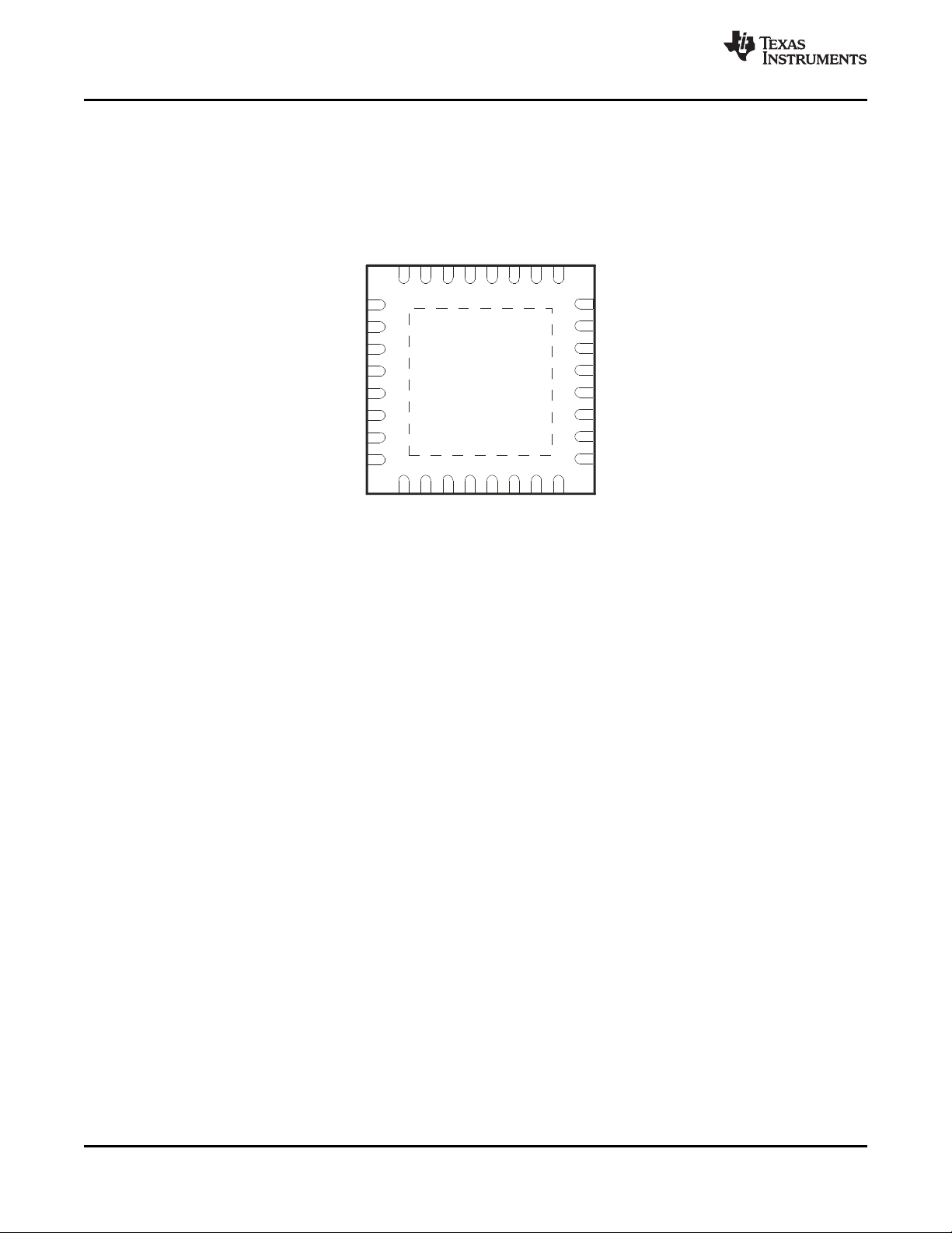
Page 10
1
2
3
4
5
6
7
8
24
23
22
21
20
19
18
17
9 10 11 12 13 14 15 16
VREF2
VBST2
VSW
REFIN2
VOUT1
VFB1
TRIP1
PGOOD1
EN1
DRVH1
LL1
252627
282930
3132
TONSEL
V5FILT
EN_LDO
VREF3
VIN
LDO
LDOREFIN
DRVL2
NC
GND
PGND
V5DRV
DRVL1
VBST1
TRIP2
VOUT2
SKIPSEL
PGOOD2
EN2
DVRH2
LL2
TPS51427
RHB PACKAGE
(TOP VIEW)
TPS51427
SLUS819B – APRIL 2008 – REVISED SEPTEMBER 2008 ................................................................................................................................................
QFN-32, 5-mm × 5-mm
(TOP VIEW)
www.ti.com
NC = No connection.
10 Submit Documentation Feedback Copyright © 2008, Texas Instruments Incorporated
Product Folder Link(s): TPS51427
Page 11
140°C
/125°C
TPS51427
www.ti.com
................................................................................................................................................ SLUS819B – APRIL 2008 – REVISED SEPTEMBER 2008
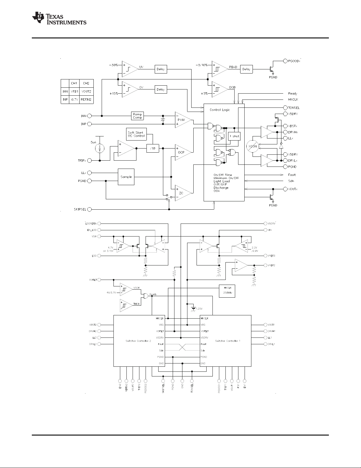
FUNCTIONAL BLOCK DIAGRAMS
Copyright © 2008, Texas Instruments Incorporated Submit Documentation Feedback 11
Product Folder Link(s): TPS51427
Page 12

( )
f
VIN VOUT VOUT
OUT(LL)
SW VIN
V V V
1
I
2 L V
æ ö
- ´
æ ö
= ´
ç ÷
ç ÷
ç ÷
´ ´
è ø
è ø
TPS51427
SLUS819B – APRIL 2008 – REVISED SEPTEMBER 2008 ................................................................................................................................................
www.ti.com
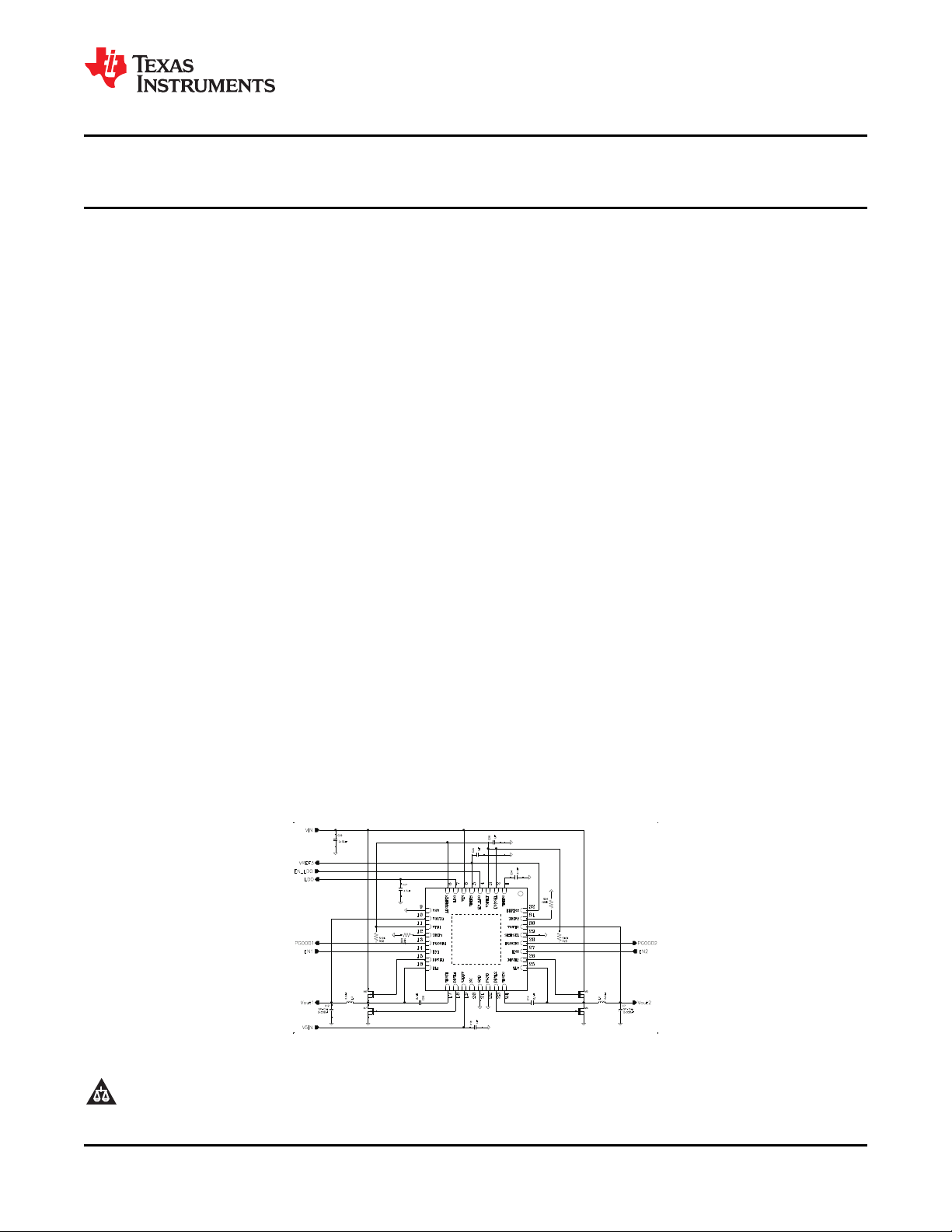
DETAILED DESCRIPTION
BASIC PWM OPERATION
The main control loop of the TPS51427 is designed as an adaptive on-time pulse width modulation (PWM)
controller. It supports a proprietary D-CAP™ mode that uses internal compensation circuitry and is suitable for a
minimal external component count configuration when an appropriate amount of ESR at the output capacitor(s) is
allowed. D-CAP mode can also enable stable operation when using capacitors with low ESR, such as specialty
polymer capacitors.
The basic operation of D-CAP mode can be described in this way: At the beginning of each cycle, the
synchronous high-side MOSFET turns on or goes to an ON state. This MOSFET turns off, or returns to an OFF
state, after an internal one-shot timer expires. The one-shot timer is determined by VIN and VOUT and keeps the
frequency fairly constant over the input voltage range under steady-state conditions; it is an adaptive on-time
control or fixed-frequency emulated on-time control. The MOSFET turns on again when the following two
conditions occur:
• Feedback information, monitored at the VFB1/VOUT2 voltage, indicates insufficient output voltage; and
• the inductor current information indicates that current is below the overcurrent limit.
Operating in this manner, the controller regulates the output voltage. The synchronous low-side or the rectifying
MOSFET is turned on each OFF state to keep the conduction loss minimum.
LIGHT LOAD CONDITIONS
The TPS51427 supports three selectable operating modes: PWM-only, Out-Of-Audio ( OOA™), and Auto-Skip.
If the SKIPSEL pin is connected to GND, Auto-Skip mode is selected. This mode enables a seamless transition
to the reduced frequency operation under light load conditions so that high efficiency is maintained over a wide
range of load current. This frequency reduction is achieved smoothly and without an increase in V
load regulation.
Auto-Skip operation can be described in this way: As the output current decreases from a heavy load condition,
the inductor current is also reduced. Eventually, the inductor current reaches the point that its valley equals zero
current; that is, the boundary between continuous conduction and discontinuous conduction modes. The
rectifying MOSFET turns off when this zero inductor current is detected. Because the output voltage remains
higher than the reference voltage at this point, both high-side and low-side MOSFETs are turned off and wait for
the next cycle. As the load current decreases further, the converter runs in discontinuous conduction mode and
takes longer to discharge the output capacitor below the reference voltage. Note that the ON time remains the
same as that in the heavy load condition. On the other hand, when the output current increases from a light load
to a heavy load, the switching frequency increases to the preset value as the inductor current reaches the
continuous conduction limit. The transition load point to the light load operation I
OUT(LL)
(that is, the threshold
between continuous conduction and discontinuous conduction mode) can be calculated as shown in Equation 1 :
ripple or
OUT
Where f
condition is a function of L, fSW, V
from the I
is the PWM switching frequency. Switching frequency versus output current under a light load
SW
threshold. For example, the frequency is approximately 60 kHz at I
OUT(LL)
IN
, and V
, but decreases at a near-proportional rate to the output current
OUT
/5 if the PWM switching
OUT(LL)
frequency is 300 kHz.
PWM-only mode is selected if the SKIPSEL pin is connected to 5 V. The rectifying MOSFET does not turn off
when the inductor current reaches zero. The converter runs in forced continuous conduction mode over the
entire load range. System designers may want to use this mode to avoid certain frequencies under light load
conditions but do so at the cost of lower efficiency. However, keep in mind that the output has the capability to
both source and sink current in this mode. If the output terminal is connected to a voltage source that is higher
than the regulator target value, the converter sinks current from the output and boosts the charge into the input
capacitors. This operation may cause an unexpected high voltage at VIN and may damage the power FETs.
If SKIPSEL pin is connected to VREF2 or left floating, OOA mode operation is selected.
12 Submit Documentation Feedback Copyright © 2008, Texas Instruments Incorporated
Product Folder Link(s): TPS51427
(1)
Page 13

TPS51427
www.ti.com
................................................................................................................................................ SLUS819B – APRIL 2008 – REVISED SEPTEMBER 2008
Table 1. SKIPSEL Operating Modes
SKIPSEL GND FLOAT/VREF2 V5IN
Operating Mode Auto Skip OOA™ PWM Only
OUT-OF-AUDIO ( OOA™) OPERATION
If out-of-audio (OOA) operation is enabled, the switching frequency of the channel remains higher than the
audible frequency under any load condition, at a minimum of 22 kHz to minimize the audible noise in the system.
The TPS51427 automatically reduces switching frequencies under light load conditions. The OOA control circuit
monitors the switching period and forces the high-side MOSFET to turn on if the switching frequency goes below
the 22-kHz threshold.
The high-side MOSFET turns on even if the output voltage is higher than the target value; therefore, the output
voltage tends to be higher when operating in OOA mode. The OOA control circuit detects the overvoltage
condition and prevents the voltage from rising by re-modulating the device on time. The overvoltage condition is
detected by the VFB1/VOUT2 voltages.
The inductor current ripple (peak-to-peak) should be less than two-thirds of the OCL setting for the OOA circuit to
work properly at a 0-A load. To keep the OOA mode loop stable, the output voltage ripple cannot be too large. If
OOA mode operation is desired, the recommended output ripple voltage cannot be more than 1% of the target
dc voltage.
RAMP COMPENSATION
The TPS51427 employs an advanced ramp compensation technique in D-CAP mode to optimize jitter
performance. An internal ramp signal is added to the reference voltage to virtually increase the slope of the
VFB1/VOUT2 down ramp, which the PWM comparator uses to determine the turn-on timing.
LOW-SIDE DRIVER
The low-side driver is designed to drive high-current, low R
represented by its internal resistance: 1.2 Ω for V5DRV to DRVLx and 0.6 Ω for DRVLx to PGND. A dead time to
prevent shoot-through is generated internally between the two transistors, with the top MOSFET off and bottom
MOSFET on, and then with the bottom MOSFET off and the top MOSFET on. A 5-V bias voltage is delivered
from the V5DRV supply. The instantaneous drive current is supplied by an input capacitor connected between
V5DRV and GND. The average drive current is equal to the gate charge at V
frequency.
, N-channel MOSFET(s). The drive capability is
DS(on)
= 5 V times the switching
GS
HIGH-SIDE DRIVER
The high-side driver is also designed to drive high-current, low R
as a floating driver, a 5-V bias voltage is delivered from the V5DRV supply. The average drive current is also
calculated by the gate charge at V
= 5 V times the switching frequency. The instantaneous drive current is
GS
supplied by the floating capacitor between the VBSTx and LLx pins. The drive capability is represented by its
internal resistance: 1.0 Ω for VBSTx to DRVHx and 0.8 Ω for DRVHx to LLx.
, N-channel MOSFET(s). When configured
DS(on)
BOOSTRAP CHARGE AUTO REFRESH
Boost undervoltage protection is activated during the device ON time when the voltage difference between
DRVH and LL becomes less than 1.8 V. Upon detection of the undervoltage condition, the high-side gate driver
immediately turns off and the low-side gate driver turns on after the deadtime expires for the minimum off time in
an attempt to recharge the boost capacitor.
PWM FREQUENCY AND ADAPTIVE ON-TIME CONTROL
The TPS51427 employs an adaptive on-time control scheme and does not have a dedicated onboard oscillator.
However, the device runs with pseudo-constant frequency by feed-forwarding the input voltage and output
voltage into the on-time one-shot timer. The frequencies are set by the TONSEL terminal connection as Table 2
shows. The on-time is controlled: it is inversely proportional to the input voltage and proportional to the output
voltage, so that the duty ratio maintains technically as VOUT/VIN with the same cycle time. Although the
TPS51427 does not use VIN directly, the input voltage is monitored at the LLx pin during the ON state.
Copyright © 2008, Texas Instruments Incorporated Submit Documentation Feedback 13
Product Folder Link(s): TPS51427
Page 14

TPS51427
SLUS819B – APRIL 2008 – REVISED SEPTEMBER 2008 ................................................................................................................................................
www.ti.com
Table 2. TONSEL Terminal Connection Options
TONSEL GND VREF2 or Float V5FILT
Channel1 Frequency 400 kHz 400 kHz 200 kHz
Channel2 Frequency 500 kHz 300 kHz 300 kHz
ENABLE AND SOFT START
TPS51427 has an internal digital soft-start timer that begins to ramp up to the maximum allowed current limit
during device startup. The soft-start ramp occurs in five steps of positive current limit; step sizes are 20%, 40%,
60%, 80%, and 100%. Smooth control of the output voltage during device startup is maintained. In addition, if
tracking discharge is required, the ENx pin can be used to control the output voltage discharge smoothly. At the
beginning of the soft-start period, the rectifying MOSFET maintains an off state until the top MOSFET turns on at
least once. This architecture prevents a high negative current from flowing back from the output capacitor in the
event of an output capacitor pre-charged condition.
If EN1 is connected to VREF2, Channel1 starts up after the Channel2 reaches regulation (delay start). If EN2 is
connected to VREF2, Channel2 starts up after the Channel1 reaches regulation (delay start).
When both ENx are low and ENLDO is low, the TPS51427 enters a shutdown state and consumes less than
15 µ A.
POWER-GOOD AND OUT-OF-BOUND OPERATION
The TPS51427 has a power-good output (PGOODx) for each switching channel. The power-good function
activates after the soft start finishes. If the output voltage reaches within ± 95% of the target value, internal
comparators detect a power-good state and the power-good signal goes high after a 1-ms internal delay. If the
output voltage falls below 90% of the target value, the power-good signal goes low after a 10- µ s internal delay.
When the output voltage exceeds +5% above of the target value while SKIPSEL is selected as auto-skip or OOA
skip-mode, the out-of-bound operation starts. During the out-of-bound condition, the controller operates in forced
PWM-only mode. Turning on the low-side MOSFET beyond the zero inductor current quickly discharges the
output capacitor. During this operation, the cycle-by-cycle negative overcurrent limit is also valid. Once the output
voltage becomes back within regulation range, the controller resumes to auto-skip or OOA skip mode."
OUTPUT SHUTDOWN AND DISCHARGE CONTROL
The TPS51427 discharges the output when ENx is low, or when the controller is shut down by the circuit
protection functions (OVP, UVP, UVLO, and thermal shutdown). The TPS51427 discharges the outputs using an
internal, 17- Ω MOSFET that is connected to VOUTx and PGND. The external low-side MOSFET does not turn
on during the output discharge operation to avoid the possibility of causing a negative voltage at the output. The
output discharge time constant is a function of the output capacitance and the resistance of the internal
discharge MOSFET. This discharge ensures that on device restart, the regulated voltage always starts from 0 V.
If an SMPS restarts before the discharge completes, the discharge action is terminated and switching resumes
after the reference level (ramped up by an internal digital-to-analog converter, or DAC) returns to the remaining
output voltage. When shutdown mode activates, the 3.3-V VREF3 remains on.
2-V REFERENCE (VREF2)
The 2-V reference is useful for generating auxiliary voltages. The tolerance for this reference voltage is ± 1.25%
over a 50- µ A load and – 40 ° C to +85 ° C ambient temperature range. This reference is enabled when ENLDO
goes high, and shuts down after both switching channels are turned off and ENLDO is shut down. If this output is
forcibly tied to ground, both SMPSs are turned off without a latch. Bypass the VREF2 pin to GND with a
minimum 0.1- µ F ceramic capacitor.
3-V REFERENCE (VREF3)
The 3.3-V reference (VREF3) is accurate to ± 1.5% over temperature, making VREF3 useful as a precision
system reference for the real-time clock (RTC) circuit in many notebook applications. VREF3 can supply up to 10
mA for external loads. Bypass VREF3 to GND with a 1- µ F capacitor. VREF3 is activated when VIN rises above
2.1 V, and remains on even when the SMPS and LDO are both shut down. VREF3 is deactivated if VIN falls
below 1.8 V. In thermal shutdown conditions, VREF3 remains activate.
14 Submit Documentation Feedback Copyright © 2008, Texas Instruments Incorporated
Product Folder Link(s): TPS51427
Page 15

( )
LDO min
LDO
5 V
C 4.7 F
V
= ´ m
( )
f
VIN VOUT VOUT
RIPPLE
OCP TRIP TRIP
VIN
V V V
I
1
I I I
2 2 L V
æ ö
- ´
æ ö
æ ö
= + = + ´
ç ÷
ç ÷
ç ÷
ç ÷
´ ´
è ø
è ø
è ø
TPS51427
www.ti.com
................................................................................................................................................ SLUS819B – APRIL 2008 – REVISED SEPTEMBER 2008
LDO
When the LDOREFIN pin is connected to GND, the TPS51427 internal linear regulator produces a fixed 5-V LDO
output; when LDOREFIN is connected to V5FILT, the linear regulator produces a fixed 3.3-V LDO output. The
LDO regulator can supply up to 100 mA for external loads. Bypass the LDO with a minimum 4.7- µ F ceramic
capacitor. When the LDO is fixed at 5 V, and VSW voltage is equal to or greater than 4.7 V, the 5 V LDO
switches off after a 3.8-ms delay, and the 5V rail is bootstrapped to the VSW output, thereby improving the
efficiency of the converter. A glitch-free switchover is also accomplished. The switchover impedance from the
VSW pin to the LDO pin is typically 0.7 Ω . In the same way, when the LDO is fixed at 3.3-V and the VSW voltage
is equal to or greater than 3.15 V, the 3.3-V LDO switches off after a delay of 4 ms, and the 3.3-V rail is
bootstrapped to the VSW output.
In adjustable mode, the LDO output can be set from 0.7 V to 4.5 V. The LDO output voltage is equal to two times
the LDOREFIN voltage. There is no switchover action in adjustable mode.
For the 5-V LDO output, a 4.7- µ F ceramic capacitor (minimum) is required from the LDO to GND. For the 3.3-V
LDO output, a 10- µ F ceramic capacitor (minimum) is required from the LDO to GND. If a lower voltage LDO
output is desired, scale the output capacitance of the LDO according to Equation 2 .
For example, if V
= 1 V, C
LDO
LDO(min)
= 23.5 µ F. Use the standard capacitance value to choose 27 µ F for the 1-V
LDO output.
CURRENT SENSING AND OVERCURRENT PROTECTION
In order to provide the most cost-effective solution, the TPS51427 supports low-side MOSFET R
overcurrent protection. In any setting, the output signal of the current amplifier becomes 100 mV at the
overcurrent limit (OCL) set point. This configuration means that the current sensing amplifier normalizes the
current information signal based on the OCL setting.
The TPS51427 supports cycle-by-cycle OCL control. The controller does not allow the next ON cycle while the
current level is above the trip threshold. The overcurrent trip threshold voltage is determined by the TRIPx pin as
Table 3 shows. The TRIPx terminal sources 5- µ A current with a 2900ppm/ ° C temperature slope, with respect to
its +25 ° C value, to compensate the temperature dependency of the MOS R
voltage across R
when TRIPx is between 200 mV and 2 V at room temperature. When the TRIPx pin is tied
TRIPx
. The trip level is set to the
DS(on)
to 5 V directly, the controller defaults to 100 mV fixed OCL setting. With this option, temperature compensation is
not obtained.
sensing for
DS(on)
(2)
OCL threshold in R
Temperature Coefficient (ppm/ ° C) 2900 None
The overcurrent condition is detected during the OFF state; therefore, I
current. Thus, the load current at overcurrent threshold, I
Copyright © 2008, Texas Instruments Incorporated Submit Documentation Feedback 15
TRIPx 0.2 V to 2 V 5 V
Table 3. Overcurrent Trip Threshold Voltage
sensing 20 mV to 200 mV 100 mV
DS(on)
, can be calculated in Equation 3 .
OCP
Product Folder Link(s): TPS51427
sets the valley level of the inductor
TRIP
(3)
Page 16

TPS51427
SLUS819B – APRIL 2008 – REVISED SEPTEMBER 2008 ................................................................................................................................................
www.ti.com
In an overcurrent condition, the current to the load exceeds the current to the output capacitor. As a result, the
output voltage tends to drop, and ends up crossing the undervoltage protection threshold, and the device shuts
down.
The TPS51427 also supports a cycle-by-cycle negative overcurrent limit in PWM-only mode. The negative
overcurrent limit is set to be negative, but at the same absolute value as the positive overcurrent limit. If the
output voltage continues to rise, the bottom MOSFET is always on; the inductor current reduces and reverse
direction after it reaches zero. When there is too much negative current in the inductor, the bottom MOSFET
turns off and a new on-time period is initiated; that is, the top MOSEFET turns on to allow current to flow into
VIN. After the on-time expires, the bottom MOSFET turns on again. This protection ensures a maximum
allowable discharge capability when the output voltage continues to rise, effectively reducing the possibility of the
overvoltage protection (OVP) circuitry.
OVERVOLTAGE/UNDERVOLTAGE PROTECTION
The TPS51427 monitors the feedback voltage for Channel1 and output voltage for Channel2 to detect both overand undervoltage conditions. When the output voltage becomes 15% higher than the target value, the OVP
comparator output goes high after a 10- µ s propagation delay; the circuit then latches the top MOSFET driver off
and the bottom MOSFET driver on, until the negative OCL limit is reached. At that time, the bottom MOSFET
turns off and the top MOSFET turns on for the minimum on-time. Once the minimum on-time expires, the bottom
MOSFET turns on again. This process repeats until the valley current of the inductor is above the negative
overcurrent limit. Once the inductor valley current is greater than the OCL, the bottom MOSFET remains on until
it is reset. Upon OVP activation, both PGOODx outputs are pulled low.
When the voltage becomes lower than 70% of the target voltage, the undervoltage protection (UVP) comparator
output goes high and an internal UVP delay counter begins counting. After 1 ms, the TPS51427 latches both top
and bottom MOSFETs off and shuts off the other channel as well. This function is enabled after the device soft
start completes.
UNDERVOLTATGE LOCKOUT (UVLO) PROTECTION
The TPS51427 has V5FILT undervoltage lockout (UVLO) protection. When the V5FILT voltage is lower than the
UVLO threshold voltage, the TPS51427 shuts off. This feature is a non-latched protection circuit.
THERMAL SHUTDOWN
The TPS51427 monitors the temperature of the die itself. If the temperature exceeds the threshold value
(typically +140 ° C), the TPS51427 shuts down. This feature is a non-latched protection circuit.
16 Submit Documentation Feedback Copyright © 2008, Texas Instruments Incorporated
Product Folder Link(s): TPS51427
Page 17

0.001
0
101
20
h – Efficiency – %
0.10.01
60
80
40
100
VIN(V)
8
12
20
I
OUT
– Output Current – A
CH1
Auto-Skip Mode
V
TONSEL
= V5FILT
0.001
0
101
20
h – Efficiency – %
0.10.01
60
80
40
100
VIN(V)
8
12
20
I
OUT
– Output Current – A
CH2
Auto-Skip Mode
V
TONSEL
= V5FILT
0.001
0
101
20
h – Efficiency – %
0.10.01
60
80
40
100
I
OUT
– Output Current – A
VIN(V)
8
12
20
CH1
OOA Mode
V
TONSEL
= V5FILT
0.001
0
20
h – Efficiency – %
60
80
40
100
I
OUT
– Output Current – A
101
VIN(V)
8
12
20
0.10.01
CH2
OOA Mode
V
TONSEL
= V5FILT
TPS51427
www.ti.com
SYSTEM DUAL RAILS
................................................................................................................................................ SLUS819B – APRIL 2008 – REVISED SEPTEMBER 2008
TYPICAL CHARACTERISTICS
EFFICIENCY EFFICIENCY
vs vs
OUTPUT CURRENT OUTPUT CURRENT
Figure 1. 5-V Efficiency in Auto-Skip Mode Figure 2. 3.3-V Efficiency in Auto-Skip Mode
EFFICIENCY EFFICIENCY
vs vs
OUTPUT CURRENT OUTPUT CURRENT
Copyright © 2008, Texas Instruments Incorporated Submit Documentation Feedback 17
Figure 3. 5-V Efficiency in OOA Mode Figure 4. 3.3-V Efficiency in OOA Mode
Product Folder Link(s): TPS51427
Page 18

0.001
0
101
20
h – Efficiency – %
0.10.01
60
80
40
100
VIN(V)
8
12
20
I
OUT
– Output Current – A
CH1
PWM Mode
V
TONSEL
= V5FILT
0.001
0
20
h – Efficiency – %
60
80
40
100
I
OUT
– Output Current – A
1010.10.01
CH2
PWM Mode
V
TONSEL
= V5FILT
VIN(V)
8
12
20
Auto-skip, 8 A
OOA, 8 A
OOA, 0 A
PWM Only, 0 A
Auto-skip, 0A
OOA, 8 A
PWM Only, 8 A
5
5.03
2520
VIN– Input Voltage – V
5.04
5.10
5.12
5.14
V
OUT
– Output Voltage – V
1510
5.08
5.11
5.06
5.05
5.07
5.09
5.13
5
3.20
2520
VIN– Input Voltage – V
3.22
3.24
3.28
3.32
3.34
3.38
3.40
3.42
V
OUT
– Output Voltage – V
1510
Mode, I
OUT
(A)
Auto-skip, 8 A
Auto-skip, 0A
OOA, 8 A
OOA, 0 A
PWM Only, 8A
PWM Only, 0A
Auto-skip, 8 A
Auto-skip, 0A
OOA, 8 A
OOA, 0 A
PWM Only, 8 A
3.30
3.36
3.26
TPS51427
SLUS819B – APRIL 2008 – REVISED SEPTEMBER 2008 ................................................................................................................................................
www.ti.com
TYPICAL CHARACTERISTICS (continued)
EFFICIENCY EFFICIENCY
OUTPUT CURRENT OUTPUT CURRENT
vs vs
Figure 5. 5-V Efficiency in PWM Mode Figure 6. 3.3-V Efficiency in PWM Mode
OUTPUT VOLTAGE OUTPUT VOLTAGE
vs vs
INPUT VOLTAGE INPUT VOLTAGE
18 Submit Documentation Feedback Copyright © 2008, Texas Instruments Incorporated
Figure 7. 5-V Line Regulation Figure 8. 3.3-V Line Regulation
Product Folder Link(s): TPS51427
Page 19

0.001
4.98
1010.01
OOA
Auto-Skip
PWM Only
I
OUT
– Output Current – mA
V
OUT
– Output Voltage – V
5.00
5.02
5.06
5.08
5.10
5.12
5.14
5.16
5.18
Mode
OOA
Auto-Skip
PWM Only
5.04
0.1
CH1
V
IN
= 12 V
V
TONSEL
= V5FILT
0.001
3.24
1010.01
OOA
Auto-Skip
PWM Only
I
OUT
– Output Current – mA
V
OUT
– Output Voltage – V
3.26
3.28
3.30
3.32
3.34
3.36
3.38
3.40
3.42
Mode
OOA
Auto-Skip
PWM Only
0.1
CH2
V
IN
= 12 V
V
TONSEL
= V5FILT
0.001
0
101
20
h – Efficiency – %
0.10.01
60
80
40
100
VIN(V)
8
12
20
I
OUT
– Output Current – A
CH1
Auto-Skip Mode
V
TONSEL
= GND
10
30
50
70
90
0.001
0
101
20
h – Efficiency – %
0.10.01
60
80
40
100
VIN(V)
8
12
20
I
OUT
– Output Current – A
CH2
Auto-Skip Mode
V
TONSEL
= GND
10
30
50
70
90
TPS51427
www.ti.com
................................................................................................................................................ SLUS819B – APRIL 2008 – REVISED SEPTEMBER 2008
TYPICAL CHARACTERISTICS (continued)
OUTPUT VOLTAGE OUTPUT VOLTAGE
OUTPUT CURRENT OUTPUT CURRENT
vs vs
Figure 9. 5-V Load Regulation Figure 10. 3.3-V Load Regulation
LOW VOLTAGE DUAL RAILS
EFFICIENCY EFFICIENCY
OUTPUT CURRENT OUTPUT CURRENT
Figure 11. 1.5-V Efficiency in Auto-Skip mode Figure 12. 1.05-V Efficiency in Auto-Skip Mode
Copyright © 2008, Texas Instruments Incorporated Submit Documentation Feedback 19
vs vs
Product Folder Link(s): TPS51427
Page 20

0.001
0
20
h – Efficiency – %
60
80
40
100
I
OUT
– Output Current – A
101
VIN(V)
8
12
20
0.10.01
CH1
OOA Mode
V
TONSEL
= GND
10
30
50
70
90
0.001
0
101
20
h – Efficiency – %
0.10.01
60
80
40
100
VIN(V)
8
12
20
I
OUT
– Output Current – A
CH2
Auto-Skip Mode
V
TONSEL
= GND
0.001
0
101
20
h – Efficiency – %
0.10.01
60
80
40
100
VIN(V)
8
12
20
I
OUT
– Output Current – A
CH1
PWM Mode
V
TONSEL
= GND
0.001
0
20
h – Efficiency – %
60
80
40
100
I
OUT
– Output Current – A
1010.10.01
CH2
PWM Mode
V
TONSEL
= GND
VIN(V)
8
12
20
TPS51427
SLUS819B – APRIL 2008 – REVISED SEPTEMBER 2008 ................................................................................................................................................
www.ti.com
TYPICAL CHARACTERISTICS (continued)
EFFICIENCY EFFICIENCY
OUTPUT CURRENT OUTPUT CURRENT
vs vs
Figure 13. 1.5-V Efficiency in OOA mode Figure 14. 1.05-V Efficiency in OOA mode
EFFICIENCY EFFICIENCY
vs vs
OUTPUT CURRENT OUTPUT CURRENT
20 Submit Documentation Feedback Copyright © 2008, Texas Instruments Incorporated
Figure 15. 1.5-V Efficiency in PWM mode Figure 16. 1.05-V Efficiency in PWM mode
Product Folder Link(s): TPS51427
Page 21

Mode, I
OUT
(A)
Auto-skip, 8 A
Auto-skip, 0A
OOA, 8 A
OOA, 0 A
PWM Only, 8A
PWM Only, 0A
5
1.495
2520
VIN– Input Voltage – V
1.500
1.515
1.525
1.530
V
OUT
– Output Voltage – V
1510
Auto-skip, 8 A
OOA, 8 A
OOA, 0 A
PWM Only, 0 A
1.510
1.520
1.505
Auto-skip, 0A
PWM Only, 8 A
5
1.050
2520
VIN– Input Voltage – V
1.055
1.075
V
OUT
– Output Voltage – V
1510
1.065
1.070
1.060
1.080
Mode, I
OUT
(A)
Auto-skip, 10 A
Auto-skip, 0A
OOA, 10 A
OOA, 0 A
PWM Only, 10A
PWM Only, 0A
0.001
1.500
1010.01
OOA
Auto-Skip
PWM Only
I
OUT
– Output Current – A
V
OUT
– Output Voltage – V
1.505
1.515
1.520
1.525
1.530
Mode
OOA
Auto-Skip
PWM Only
1.510
0.1
CH1
V
IN
= 12 V
V
TONSEL
= GND
0.001
1.054
1010.01
OOA
Auto-Skip
PWM Only
I
OUT
– Output Current – mA
V
OUT
– Output Voltage – V
1.056
1.058
1.062
1.066
1.068
1.070
1.072
1.074
1.076
Mode
OOA
Auto-Skip
PWM Only
1.060
0.1
1.064
CH2
V
IN
= 12 V
V
TONSEL
= GND
TPS51427
www.ti.com
................................................................................................................................................ SLUS819B – APRIL 2008 – REVISED SEPTEMBER 2008
TYPICAL CHARACTERISTICS (continued)
OUTPUT VOLTAGE OUTPUT VOLTAGE
vs vs
INPUT VOLTAGE INPUT VOLTAGE
Figure 17. 1.5-V Line Regulation Figure 18. 1.05-V Line Regulation
OUTPUT VOLTAGE OUTPUT VOLTAGE
vs vs
OUTPUT CURRENT OUTPUT CURRENT
Figure 19. 1.5-V Load Regulation Figure 20. 1.05-V Load Regulation
Copyright © 2008, Texas Instruments Incorporated Submit Documentation Feedback 21
Product Folder Link(s): TPS51427
Page 22

0
3.0
20010050
VIN(V)
6
12
25
VIN= 6 V
VIN= 12 V
VIN= 25 V
I
OUT
– Output Current – mA
3.5
4.0
4.5
5.0
5.5
150
V
OUT
– Output Voltage – V
0
2.0
20010050
VIN(V)
6
12
25
VIN= 6 V
VIN= 12 V
VIN= 25 V
I
OUT
– Output Current – mA
2.5
3.0
3.5
4.0
150
V
OUT
– Output Voltage – V
0
1.991
15010050
VIN= 6 V
VIN= 12 V
VIN= 25 V
I
OUT
– Output Current – mA
V
VREF
– Voltage Reference – V
1.992
1.993
1.994
1.995
1.996
1.997
1.998
1.999
2.000
VIN(V)
6
12
25
0
3.270
1073
I
OUT
– Output Current – mA
3.275
3.280
3.285
3.290
3.295
3.300
3.305
3.310
VIN= 6 V
VIN= 12 V
VIN= 25 V
V
VREF
– Voltage Reference – V
841 5 6 92
VIN(V)
6
12
25
TPS51427
SLUS819B – APRIL 2008 – REVISED SEPTEMBER 2008 ................................................................................................................................................
www.ti.com
TYPICAL CHARACTERISTICS (continued)
OUTPUT VOLTAGE OUTPUT VOLTAGE
OUTPUT CURRENT OUTPUT CURRENT
vs vs
Figure 21. 5-V LDO Load Regulation Figure 22. 3.3-V LDO Load Regulation
OUTPUT VOLTAGE OUTPUT VOLTAGE
vs vs
OUTPUT CURRENT OUTPUT CURRENT
22 Submit Documentation Feedback Copyright © 2008, Texas Instruments Incorporated
Figure 23. 2-V Reference Load Regulation Figure 24. 3.3-V Reference Load Regulation
Product Folder Link(s): TPS51427
Page 23

5
100
252010
VIN– Input Voltage – V
f
SW
– Frequency – kHz
200
300
500
400
15
V
TONSEL
(V)
V
V5FILT
GND
V
VREF2
V
TONSEL=
GND
V
TONSEL
= V
V5FILT
V
TONSEL
= V
VREF2
5
100
252010
VIN– Input Voltage – V
f
SW
– Frequency – kHz
200
300
400
15
V
TONSEL
(V)
V
V5FILT
GND
V
VREF2
V
TONSEL=
GND
V
TONSEL
= V
V5FILT
V
TONSEL
= V
VREF2
500
600
0
f
SW
– Frequency – kHz
50
200
250
100
150
OOA
Auto-Skip
CH1
VIN= 12 V
V
TONSEL
= V
V5VFILT
0.001 1010.01
I
OUT
– Output Current – A
0.1
0
f
SW
– Frequency – kHz
100
200
400
300
CH2
VIN= 12 V
V
TONSEL
= V
V5VFILT
50
150
350
250
OOA
Auto-Skip
0.001 1010.01
I
OUT
– Output Current – A
0.1
TPS51427
www.ti.com
................................................................................................................................................ SLUS819B – APRIL 2008 – REVISED SEPTEMBER 2008
TYPICAL CHARACTERISTICS (continued)
FREQUENCY FREQUENCY
vs vs
INPUT VOLTAGE INPUT VOLTAGE
Figure 25. Channel 1 (5-V Setting) Figure 26. Channel 2 (3.3-V Setting)
FREQUENCY FREQUENCY
vs vs
OUTPUT CURRENT OUTPUT CURRENT
Copyright © 2008, Texas Instruments Incorporated Submit Documentation Feedback 23
Figure 27. Load Current (5-V Setting) Figure 28. Load Current (3.3-V Setting)
Product Folder Link(s): TPS51427
Page 24

5
100
251510
VIN– Input Voltage – V
300
400
500
20
200
V
TONSEL=
GND
V
TONSEL
= V
VREF2
V
TONSEL
= V
V5FILT
V
TONSEL
(V)
GND
VREF2
V5FILT
f
SW
– Frequency – kHz
5
100
251510
V
IN
– Input Voltage – V
f
SW
– Frequency – kHz
300
400
600
20
200
500
V
TONSEL
(V)
GND
VREF2
V5FILT
V
TONSEL
= V
VREF2
V
TONSEL
= V
V5FILT
V
TONSEL=
GND
0.001
0
1010.01
OOA
Auto-Skip
I
OUT
– Output Current – A
50
200
250
300
350
100
0.1
CH1
V
IN
= 19 V
V
TONSEL
= GND
150
f
SW
– Frequency – kHz
0.001
0
1010.01
I
OUT
– Output Current – A
50
200
250
300
350
100
0.1
CH2
V
IN
= 19 V
V
TONSEL
= GND
150
OOA
Auto-Skip
f
SW
– Frequency – kHz
TPS51427
SLUS819B – APRIL 2008 – REVISED SEPTEMBER 2008 ................................................................................................................................................
www.ti.com
TYPICAL CHARACTERISTICS (continued)
FREQUENCY FREQUENCY
vs vs
INPUT VOLTAGE INPUT VOLTAGE
Figure 29. Channel 1 (1.5-V Setting) Figure 30. Channel 2 (1.05-V Setting)
FREQUENCY FREQUENCY
vs vs
OUTPUT CURRENT OUTPUT CURRENT
Figure 31. Load Current (5-V Setting) Figure 32. Load Current (3.3-V Setting)
24 Submit Documentation Feedback Copyright © 2008, Texas Instruments Incorporated
Product Folder Link(s): TPS51427
Page 25

0
150
531
V
TONSEL=
GND
V
OUT
– Output Voltage – V
f
SW
– Frequency – kHz
200
300
400
450
4
V
TONSEL
(V)
GND
2
5
250
350
2
V
TONSEL=
2 V
V
TONSEL=
5 V
0
200
3.0
1.5
0.5
V
TONSEL=
GND
V
OUT
– Output Voltage – V
f
SW
– Frequency – kHz
250
350
450
500
2.5
V
TONSEL
(V)
GND
2
5
300
400
1.0
V
TONSEL=
2 V
V
TONSEL=
5 V
2.0
TPS51427
www.ti.com
................................................................................................................................................ SLUS819B – APRIL 2008 – REVISED SEPTEMBER 2008
TYPICAL CHARACTERISTICS (continued)
FREQUENCY FREQUENCY
OUTPUT VOLTAGE OUTPUT VOLTAGE
vs vs
Figure 33. Channel 1 Setting Figure 34. Channel 2 Setting
Copyright © 2008, Texas Instruments Incorporated Submit Documentation Feedback 25
Product Folder Link(s): TPS51427
Page 26

TPS51427
SLUS819B – APRIL 2008 – REVISED SEPTEMBER 2008 ................................................................................................................................................
www.ti.com
TYPICAL CHARACTERISTICS (continued)
Figure 35. Channel 1 Gate Driver Performance Figure 36. Channel 2 Gate Driver Performance
Figure 37. Channel 1 Load Step Figure 38. Channel 1 Load Release
Figure 39. Channel 2 Load Step Figure 40. Channel 2 Load Release
26 Submit Documentation Feedback Copyright © 2008, Texas Instruments Incorporated
Product Folder Link(s): TPS51427
Page 27

TPS51427
www.ti.com
................................................................................................................................................ SLUS819B – APRIL 2008 – REVISED SEPTEMBER 2008
APPLICATION INFORMATION
Table 4. List of Materials
COMPONENTS CONFIGURATION NO. 1 CONFIGURATION NO. 2 CONFIGURATION NO. 3
400 kHz/300 kHz Channel1: 5 400 kHz/500 kHz Channel1: 400kHz/500kHz Channel1:
V/8 A (fixed) Channel2: 3.3 V/10 1.5V/10A (fixed) Channel2: 1.05 1.8V/10A (adj) Channel2:
A (fixed) V/15 A(fixed) 1.1V/15A (adj)
Input voltage 8 V ≤ VIN≤ 22 V
Input MLCC capacitors Murata Murata Murata
Channel1
Output capacitor
Output inductor
High-side MOSFET
Low-side MOSFET IRF7811AV, 30 V, 10.8 A, 0.011
R
OCL
R
UPPER_DIV
R
LOWER_DIV
Channel2
Output capacitor
Output inductor
High-side MOSFET
Low-side MOSFET
R
OCL
R
UPPER_DIV
R
LOWER_DIV
4 x 10 µ F, 25 V 4 x 10 µ F, 25 V 4 x 10 µ F, 25 V
GRM31CR61E106KA12L GRM31CR61E106KA12L GRM31CR61E106KA12L
1 x 330 µ F, 6 V, 25 m Ω , Sanyo, 2 x 330 µ F, 2.5 V, 12 m Ω , 2 x 330 µ F, 2.5 V, 12 m Ω ,
6TPE330ML Sanyo, 2R5TPE330MC Sanyo, 2R5TPE330MC
Sumida, 4.3 µ H, Sumida, 2.2 µ H, Sumida, 2.2 µ H,
CEP125NP-4R3M-U, 11.4 m Ω CEP125NP-2R2M-U, 5.4 m Ω CEP125NP-2R2M-U, 5.4 m Ω
International Rectifier, IRF7807V, International Rectifier, IRF7807V, International Rectifier, IRF7807V,
30 V, 8.3 A, 0.017 Ω 30V, 8.3A, 0.017 Ω 30V, 8.3A, 0.017 Ω
International Rectifier,
Ω
International Rectifier, IRF7832, International Rectifier, IRF7832,
30V, 20A, 0.004 Ω 30V, 20A, 0.004 Ω
267 k Ω for OCL of 10 A to 14 A 110 k Ω for OCL of 12 A to 18 A 110 k Ω for OCL of 12 A to 18 A
Tie VFB1 to GND Tie VFB1 to V5FILT
1 x 330 µ F, 4 V, 18 m Ω Sanyo, 2 x 470 µ F, 2.5 V, 9 m Ω , Sanyo, 2 x 470 µ F, 2.5 V, 9 m Ω , Sanyo,
4TPE330MI 2R5TPE470M9 2R5TPE470M9
Sumida, 3.2 µ H, 8.0 m Ω , Vishay, 1 µ H, 3 m Ω , Vishay, 1 µ H, 3 m Ω ,
CEP125NP-3R2M-U IHLP5050CE IHLP5050CE
International Rectifier, IRF7807V, International Rectifier, IRF7821, International Rectifier, IRF7821,
30 V, 8.3 A, 0.017 Ω 30 V, 13 A, 0.009 Ω 30 V, 13 A, 0.009 Ω
International Rectifier, IRF7832, International Rectifier, IRF7832, International Rectifier, IRF7832,
30 V, 20 A, 0.004 Ω 30 V, 20 A, 0.004 Ω 30 V, 20 A, 0.004 Ω
110 k Ω for OCL of 12 A to 18 A 169 k Ω for OCL of 18 A to 26 A 169 k Ω for OCL of 18 A to 26 A
Tie REFIN2 to V5FILT Tie REFIN2 to VREF3
39.2 k Ω , 1%
24.9 k Ω , 1%
44.2 k Ω , 1%
54.9 k Ω
Copyright © 2008, Texas Instruments Incorporated Submit Documentation Feedback 27
Product Folder Link(s): TPS51427
Page 28

TPS51427
SLUS819B – APRIL 2008 – REVISED SEPTEMBER 2008 ................................................................................................................................................
www.ti.com
Figure 41. Configuration 1: System Rail
28 Submit Documentation Feedback Copyright © 2008, Texas Instruments Incorporated
Product Folder Link(s): TPS51427
Page 29

TPS51427
www.ti.com
................................................................................................................................................ SLUS819B – APRIL 2008 – REVISED SEPTEMBER 2008
Figure 42. Configuration 2: Low Voltage Rail (Fixed Voltage Settings)
Copyright © 2008, Texas Instruments Incorporated Submit Documentation Feedback 29
Product Folder Link(s): TPS51427
Page 30

TPS51427
SLUS819B – APRIL 2008 – REVISED SEPTEMBER 2008 ................................................................................................................................................
www.ti.com
Figure 43. Configuration 3: Low-Voltage Dual Rail (Adjustable Voltage Settings)
30 Submit Documentation Feedback Copyright © 2008, Texas Instruments Incorporated
Product Folder Link(s): TPS51427
Page 31

Switching
Logic
DRVH
TPS51427
DRVL
One Shot
Blanking
Period
+
R
FB
Q1
Q2
I
L
ESR
C
OUT
L
O
A
D
I
LOAD
V
OUT
VFB
High-Speed Comparator
VREF
UDG-08056
V
IN
Lo
I
t
ON
tONtriggered when V
OUT
declines to V
REF
level
V
RIPPLE
= I
RIPPLE
x ESR
I
LOAD
V
REF
I
RIPPLE
V
RIPPLE
TPS51427
www.ti.com
................................................................................................................................................ SLUS819B – APRIL 2008 – REVISED SEPTEMBER 2008
Loop Compensation and External Part Selection
A simplified buck converter system using D-CAP mode is shown below in Figure 44 .
Figure 44. D-CAP Mode Operation Schematic
Figure 45. D-CAP Mode Operation Waveforms
The output voltage is compared with an internal reference voltage through scaling. The PWM comparator
determines the timing to turn on the high side MOSFET. The gain and speed of the comparator is high enough to
keep the voltage at the beginning of each on cycle (or the end of off cycle) substantially constant. The DC output
voltage changes when the input voltage changes due to the fact that voltage regulation is maintained at the
valley point. Therefore, as the output ripple amplitude increases when the input voltage increases, the DC output
voltage increases as well.
Copyright © 2008, Texas Instruments Incorporated Submit Documentation Feedback 31
Product Folder Link(s): TPS51427
Page 32

SW
0
OUT
f
1
f
2 ESR C 4
= £
p´ ´
( )
( )
(
)
( )
( )
( )
(
)
( )
f f
OUT OUT OUT OUT
IN max IN max
IND ripple IN max OUT max IN max
V V V V V V
1 3
L
I V I V
- ´ - ´
= ´ = ´
´ ´
OUT
RIPPLE
1.5%
ESR VI= ´
TPS51427
SLUS819B – APRIL 2008 – REVISED SEPTEMBER 2008 ................................................................................................................................................
For loop stability, the 0-dB frequency, f0, defined in Equation 4 must be lower than of the switching frequency.
As f0is determined solely by the output capacitor ’ s characteristics, loop stability of D-CAP mode is determined by
the capacitor ’ s chemistry. For example, the output capacitance of specialty polymer capacitors (SP-CAP) is on
the order of several hundred microfarads and an ESR of approximately 10 m Ω . These values yield a 0-dB
frequency of 100 kHz or less and the loop is stable. However, ceramic capacitors yield a f0at more than 700 kHz
which is not suitable for this operational mode.
Although D-CAP mode provides many advantages such as ease-of-use, minimum external components, and
extremely fast transient response, a sufficient amount of feedback signal needs to be provided to reduce the jitter
level. In a TPS51427 design, it is generally recommended to optimize the output voltage ripple at around 1.5% of
the targeted DC voltage in both Auto-skip and PWM mode operations. For example, if V
desired output ripple should be at least 1.5 V x 1.5% = 22.5 mV. This can be achieved by taking advantage of
the output bulk capacitor ESR.
The external component selection is much simpler in D-CAP mode. Below is a simplified design procedure
targeting to the customers that are very familiar with SMPS design.
1. Determine the output voltage setting.
For the fixed 5 V/3.3 V option, tie VFB1 pin to GND and REFIN2 to V5FILT. For the fixed 1.5 V/1.05 V
configuration, tie VFB1 to V5FILT and REFIN2 to VREF3. TPS51427 also supports adjustable voltage
options for both channels. The adjustable range for Channel1 is between 0.7 V and 5.9 V and for Channel2
is between 0.5 V and 2.5 V. Figure 46 shows how to configure the adjustable voltage option for Channel1
and Figure 47 shows the configuration for Channel2. Also, equations are provided in Table 5 to aid the
design process.
2. Choose the output inductor.
Output inductance is a function of V
frequency settings with TPS51427, refer to Table 2 . The process of choosing the right output inductance is
an iterative one; many considerations need to be taken, such as the desired transient response, efficiency
over the entire load range, load/line regulation, component availability and cost. Base the initial output
inductance value upon where the ripple current is 25% to 50% of the maximum loading current. For transient
optimized design, ripple factor can be higher; and for efficiency and load/line regulation optimized design, the
ripple factor can be lower.
, V
, f
IN
OUT
and the desired ripple current. For available switching
SW
VOUT1
www.ti.com
= 1.5 V, the
(4)
3. Choose the output capacitor(s).
Organic semiconductor capacitors or specialty polymer capacitor(s) are recommended. Determine ESR to
meet the required ripple voltage indicated previous.
32 Submit Documentation Feedback Copyright © 2008, Texas Instruments Incorporated
Product Folder Link(s): TPS51427
(5)
(6)
Page 33

( )
( )
LOW ER _DI V VREF2
REFIN2
UPPE R _D IV LO WER _ DIV
R V
V
R R
æ ö
´
ç ÷
=
ç ÷
+
è ø
UPPER _ DIV LO WER _DIV
VOUT1 V FB1
LOWE R _ DIV
R R
V V
R
æ ö
+
ç ÷
= ´
ç ÷
è ø
10
11
VOUT1
VFB1
R
UPPER_DIV
R
LOWER_DIV
TPS51427
VBAT
UDG-08059
30
1
32
VOUT2
VREF2
REFIN2
R
UPPER_DIV
R
LOWER_DIV
TPS51427
VBAT
UDG-08060
TPS51427
www.ti.com
ADJUSTABLE
................................................................................................................................................ SLUS819B – APRIL 2008 – REVISED SEPTEMBER 2008
FIXED
VOLTAGE 5 V by shorting VFB1 to GND
OPTIONS
VOUT1 is set by R
VOLTAGE
OPTIONS
where
• V
Table 5. Design Assistance
Channel1 Channel2
1.5 V by shorting VFB1 to 3.3 V by shorting 1.05 V by shorting
UPPER_DIV
, R
LOWER_DIV
V5FILT REFIN2 to V5FILT REFIN2 to VREF3
, and VFB1 Figure 46
VOUT2 is set by R
UPPER_DIV
VFB1 Figure 47
(7)
, R
LOWER_DIV
, and
(8)
where
= 0.7 V
VFB1
• V
• V
= 2 V
VREF
= V
VOUT2
REFIN2
Figure 46. Channel1 Adjustable Voltage Configuration Figure 47. Channel2 Adjustable Voltage Configuration
Ripple Requirement in PWM Mode, Skip Mode and OOA Mode
Since TPS51427 is a constant on time based controller, minimum ripple requirement at the output is necessary
to keep the main voltage loop stable. For loop stability, the ESR zero frequency, f0must be lower than 1/4 of the
switching frequency. This requirement can be easily fulfilled by using either POSCAP or SPCAP, due to their
similar characteristics. In order for a constant on time topology to work properly in a real world environment,
there should not be any substantial phase delay contributed by the parasitic model of the output capacitors. Such
delay would create distortion to the essential feedback signal necessary for the device to process.
In a TPS51427 design, it is generally recommended to optimize the output voltage ripple at around 1.5% of the
targeted DC voltage in both auto-skip and PWM mode operations. Higher ripple is better in terms of jitter
performance, however, lower ripple improves the line regulation and efficiency performance. It is a common
practice as an attainable goal to optimize the converter design in terms of regulation and efficiency.
There is an additional voltage loop in the TPS51427 design that needs to be considered. OOA (out-of-audio)
mode is designed to keep the minimum switching frequency at least 22 kHz in the light load/no load operation in
order to minimize the audible noise in the notebook system design during standby mode. Both main voltage loop
and OOA loop require certain output ripple in order for the device to function properly. If the ripple is too low, the
main loop is unstable. If OOA mode operation is desired, the recommended ripple cannot be more than 1% of
the target DC voltage.
Copyright © 2008, Texas Instruments Incorporated Submit Documentation Feedback 33
Product Folder Link(s): TPS51427
Page 34

( ) ( )
OCLx
DS on max MIN OCLvalley
V R I= ´
OCLx
OCLx
TRIP
V 5mV
R 10
I
æ ö
+
= ´
ç ÷
è ø
TRIPx TRIP OCLx
V I R= ´
( )
( )
( )
TRIPx(max) TRIP OCLx J
V I R 1 TOL 1 2900ppm / C T 25 C= ´ ´ + ´ + ° ´ - °
TPS51427
SLUS819B – APRIL 2008 – REVISED SEPTEMBER 2008 ................................................................................................................................................
www.ti.com
Current Limit Design Considerations
The current limit of Channel1 can be set using the TRIP1 pin via an external small resistor to GND. Channel2
current limit can be set via the TRIP2 pin. The sourcing current for both Channel1 and Channel2 is 5 µ A at room
temperature with 2900 ppm/ ° C built-in temperature coefficient (to compensate for the temperature dependency of
the R
TPS51427 and the low-side MOSFET has to be obtained.
The current limit adjustment range (VTRIPx) is between 0.2 V and 2 V. If 5 V is applied to the pin (TRIP1 and/or
TRIP2) directly (V
compensation.
Once the minimum OCL level is determined, translate the minimum OCL point (DC) into minimum valley current
by subtracting of the peak-to-peak inductor current. Then convert the current information into the voltage level for
the TPS51427 to process.
The external resistor can be set using Equation 10 .
Once R
pin and/or the TRIP2 pin is less than 3.1 V for the entire operating temperature range.
The TRIPx voltage (V
of the low-side MOSFET). To take advantage of this feature, a good thermal coupling between the
DS(on)
> 3.1 V), TPS51427 assumes a default of a 100-mV current limit without temperature
TRIPx
where
• the low-side MOSFET at TJ= 25 ° C
where
• I
OCLx
= 5 µ A and the tolerance is ± 5%
TRIP
is obtained, calculate the maximum V
) can be calculated by Equation 11 .
TRIPx
voltage to make sure the maximum voltage on the TRIP1
TRIPx
(9)
(10)
And maximum VTRIPx voltage can be calculated by Equation 12 .
where
• I
• TOL = 5%
• TJis assumed to be 125 ° C for the worst case junction temperature
= 5 µ A
TRIP
Shutdown and Standby Control Logic
Shutdown and Standby Control Logic Table
ENLDO LDO VREF2 VREF3 EN1 EN2 Channel1 Channel1
Low Off Low Low Low Off Off
High On On Low Low Off Off
High On On High High On On
High On On High Low On Off
High On On Low High Off On
High On On High On
High On On High On
On (if VIN> 2.2 V)
Off (if VIN< 2 V)
On (after Channel2
is up)
(11)
(12)
On (after Channel1
is up)
34 Submit Documentation Feedback Copyright © 2008, Texas Instruments Incorporated
Product Folder Link(s): TPS51427
Page 35

TPS51427
www.ti.com
................................................................................................................................................ SLUS819B – APRIL 2008 – REVISED SEPTEMBER 2008
Layout Guidelines
1. Place one or two 10- µ F ceramic capacitor(s) for V
between drain of the high-side MOSFET and source of the low-side MOSFET of each channel.
2. Place V
terminal of V
capacitors, VOUT1/VOUT2 capacitors and MOSFETs on the same side of the board. Positive
IN
capacitor and drain of the high-side MOSFET should be as close as possible (within 10 mm if
IN
possible). Also place negative terminals of both V
MOSFET as close as possible.
3. GND terminal of the device (signal GND) and PGND terminal (power GND) should be connected with the
lowest impedance near the device.
4. Trace of the switching node which is connected between the source of the high-side MOSFET, drain of the
low-side MOSFET and the upstream of the output inductor should be as short and thick as possible. Use 40
mil of width (LL1 and LL2) for every ampere of load current.
5. LL1 and LL2 serve the phase node connections for the high-side drivers. Also, they are served as input to
the current comparators for R
sensing and input voltage monitor for the on time control circuitry. Route
DS(on)
the return of these two traces to device pins as wide and short as possible to eliminate the parasitic
inductance effect to the accuracy of the measurement.
6. Place a low-pass filter MLCC capacitor with a value of 1- µ F from V5FILT to GND, as close as possible.
7. The output of LDO if configured as 5VLDO, requires at least 4.7- µ F of MLCC to GND. If it is configured as
3.3 VLDO, 10 µ F of MLCC is recommended. For optimized stability and transient response, use a value of
27 µ F if the output of LDO is configured as 1VLDO. VREF2 requires 0.1- µ F ceramic bypass capacitor to
GND which should be placed as close to the device as possible. For VREF3, it generally requires a 1- µ F
ceramic by pass capacitor to GND which also should be placed as close to the device as possible.
8. Connect the overcurrent setting resistors from TRIP1/TRIP2 to GND. The traces from TRIP1/TRIP2 should
be routed as far as possible from the switching nodes.
9. 9. In the case of adjustable output voltage with external resistor dividers, the discharge path (VOx) can share
the trace to the output capacitor with the feedback trace (VFB1/REFIN2). Please place the voltage setting
resistors as close to the device as possible. Route the VOx and feedback traces as far from the high speed
switching nodes as possible to avoid noise coupling.
10. Connections from the drivers to the respective gate of the high-side or the low-side MOSFETs should be as
short as possible to reduce stray inductance. Use 0.65 mm (25 mils) or wider trace.
11. All sensitive analog traces and components such as VO1/VO2, VFB1/REFIN2, VREF2, VREF3, EN1/EN2,
GND, VSW, PGOOD1/PGOOD2, TRIP1/TRIP2, ENLDO, LDOREFIN, V5FILT, TONSEL and SKIPSEL
should be placed away from high-voltage switching nodes such as LLx, DRVLx or DRVHx nodes to avoid
coupling. Use internal layer(s) as ground plane(s) and shield feedback traces from power traces and
components.
12. In order to effectively remove heat from the package, prepare thermal land and solder to the package ’ s
thermal pad. 3 × 3 or more vias with a 0.33-mm (13mils) diameter connected from the thermal land to the
internal ground plane should be used to help dissipation. Connect GND to the thermal land directly.
between two channels. Add 1000-pF ceramic capacitor
IN
capacitor and V
IN
capacitor, and source of the low-side
OUT
Copyright © 2008, Texas Instruments Incorporated Submit Documentation Feedback 35
Product Folder Link(s): TPS51427
Page 36

PACKAGE MATERIALS INFORMATION
www.ti.com 18-Aug-2014
TAPE AND REEL INFORMATION
*All dimensions are nominal
Device Package
Type
TPS51427RHBR VQFN RHB 32 3000 330.0 12.4 5.3 5.3 1.1 8.0 12.0 Q2
TPS51427RHBR VQFN RHB 32 3000 330.0 12.4 5.3 5.3 1.5 8.0 12.0 Q2
TPS51427RHBT VQFN RHB 32 250 180.0 12.4 5.3 5.3 1.1 8.0 12.0 Q2
TPS51427RHBT VQFN RHB 32 250 180.0 12.4 5.3 5.3 1.5 8.0 12.0 Q2
Package
Drawing
Pins SPQ Reel
Diameter
(mm)
Reel
Width
W1 (mm)
A0
(mm)B0(mm)K0(mm)P1(mm)W(mm)
Pin1
Quadrant
Pack Materials-Page 1
Page 37

PACKAGE MATERIALS INFORMATION
www.ti.com 18-Aug-2014
*All dimensions are nominal
Device Package Type Package Drawing Pins SPQ Length (mm) Width (mm) Height (mm)
TPS51427RHBR VQFN RHB 32 3000 367.0 367.0 35.0
TPS51427RHBR VQFN RHB 32 3000 367.0 367.0 35.0
TPS51427RHBT VQFN RHB 32 250 210.0 185.0 35.0
TPS51427RHBT VQFN RHB 32 250 210.0 185.0 35.0
Pack Materials-Page 2
Page 38

Page 39

Page 40

Page 41

IMPORTANT NOTICE
Texas Instruments Incorporated and its subsidiaries (TI) reserve the right to make corrections, enhancements, improvements and other
changes to its semiconductor products and services per JESD46, latest issue, and to discontinue any product or service per JESD48, latest
issue. Buyers should obtain the latest relevant information before placing orders and should verify that such information is current and
complete. All semiconductor products (also referred to herein as “components”) are sold subject to TI’s terms and conditions of sale
supplied at the time of order acknowledgment.
TI warrants performance of its components to the specifications applicable at the time of sale, in accordance with the warranty in TI’s terms
and conditions of sale of semiconductor products. Testing and other quality control techniques are used to the extent TI deems necessary
to support this warranty. Except where mandated by applicable law, testing of all parameters of each component is not necessarily
performed.
TI assumes no liability for applications assistance or the design of Buyers’ products. Buyers are responsible for their products and
applications using TI components. To minimize the risks associated with Buyers’ products and applications, Buyers should provide
adequate design and operating safeguards.
TI does not warrant or represent that any license, either express or implied, is granted under any patent right, copyright, mask work right, or
other intellectual property right relating to any combination, machine, or process in which TI components or services are used. Information
published by TI regarding third-party products or services does not constitute a license to use such products or services or a warranty or
endorsement thereof. Use of such information may require a license from a third party under the patents or other intellectual property of the
third party, or a license from TI under the patents or other intellectual property of TI.
Reproduction of significant portions of TI information in TI data books or data sheets is permissible only if reproduction is without alteration
and is accompanied by all associated warranties, conditions, limitations, and notices. TI is not responsible or liable for such altered
documentation. Information of third parties may be subject to additional restrictions.
Resale of TI components or services with statements different from or beyond the parameters stated by TI for that component or service
voids all express and any implied warranties for the associated TI component or service and is an unfair and deceptive business practice.
TI is not responsible or liable for any such statements.
Buyer acknowledges and agrees that it is solely responsible for compliance with all legal, regulatory and safety-related requirements
concerning its products, and any use of TI components in its applications, notwithstanding any applications-related information or support
that may be provided by TI. Buyer represents and agrees that it has all the necessary expertise to create and implement safeguards which
anticipate dangerous consequences of failures, monitor failures and their consequences, lessen the likelihood of failures that might cause
harm and take appropriate remedial actions. Buyer will fully indemnify TI and its representatives against any damages arising out of the use
of any TI components in safety-critical applications.
In some cases, TI components may be promoted specifically to facilitate safety-related applications. With such components, TI’s goal is to
help enable customers to design and create their own end-product solutions that meet applicable functional safety standards and
requirements. Nonetheless, such components are subject to these terms.
No TI components are authorized for use in FDA Class III (or similar life-critical medical equipment) unless authorized officers of the parties
have executed a special agreement specifically governing such use.
Only those TI components which TI has specifically designated as military grade or “enhanced plastic” are designed and intended for use in
military/aerospace applications or environments. Buyer acknowledges and agrees that any military or aerospace use of TI components
which have not been so designated is solely at the Buyer's risk, and that Buyer is solely responsible for compliance with all legal and
regulatory requirements in connection with such use.
TI has specifically designated certain components as meeting ISO/TS16949 requirements, mainly for automotive use. In any case of use of
non-designated products, TI will not be responsible for any failure to meet ISO/TS16949.
Products Applications
Audio www.ti.com/audio Automotive and Transportation www.ti.com/automotive
Amplifiers amplifier.ti.com Communications and Telecom www.ti.com/communications
Data Converters dataconverter.ti.com Computers and Peripherals www.ti.com/computers
DLP® Products www.dlp.com Consumer Electronics www.ti.com/consumer-apps
DSP dsp.ti.com Energy and Lighting www.ti.com/energy
Clocks and Timers www.ti.com/clocks Industrial www.ti.com/industrial
Interface interface.ti.com Medical www.ti.com/medical
Logic logic.ti.com Security www.ti.com/security
Power Mgmt power.ti.com Space, Avionics and Defense www.ti.com/space-avionics-defense
Microcontrollers microcontroller.ti.com Video and Imaging www.ti.com/video
RFID www.ti-rfid.com
OMAP Applications Processors www.ti.com/omap TI E2E Community e2e.ti.com
Wireless Connectivity www.ti.com/wirelessconnectivity
Mailing Address: Texas Instruments, Post Office Box 655303, Dallas, Texas 75265
Copyright © 2014, Texas Instruments Incorporated
Page 42

 Loading...