

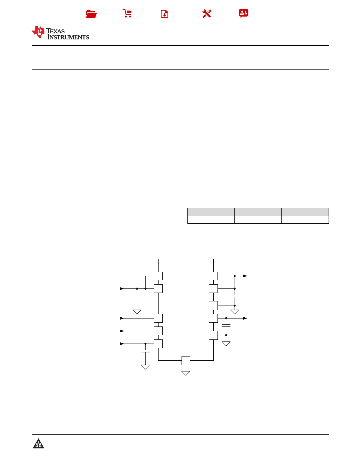
1
2
7
9
3
5
4
6
VTT
VTTSNS
PGND
VTTREF
VDDQSNS
VLDOIN
S3
S5
TPS51206
10 VDD
8GND
PowerPad
VTT
VTTREF
UDG-11024
S3_SLP
S5_SLP
5 V or 3.3 V
Supply
VDDQ
Product
Folder
Sample &
Buy
Technical
Documents
Tools &
Software
Support &
Community
TPS51206
SLUSAH1B –MAY 2011–REVISED DECEMBER 2014
TPS51206 2-A Peak Sink / Source DDR Termination Regulator With VTTREF Buffered
Reference for DDR2, DDR3 and DDR3L
1 Features 3 Description
1
• Supply Input Voltage: Supports 3.3-V Rail and 5-V
Rail
• VLDOIN Input Voltage Range: VTT+0.4 V to 3.5 V
• VTT Termination Regulator
– Output Voltage Range: 0.5 V to 0.9 V
– 2-A Peak Sink and Source Current
– Requires Only 10-μF MLCC Output Capacitor
– ±20 mV Accuracy
• VTTREF Buffered Reference
– VDDQ/2 ± 1% Accuracy
– 10-mA Sink / Source Current
• Supports High-Z in S3 and Soft-Stop in S4/S5
with S3/S5 Inputs
• Overtemperature Protection
• 10-Pin 2-mm × 2-mm SON (DSQ) Package
2 Applications
• DDR2/DDR3/DDR3L Memory Power Supplies
• SSTL_18, SSTL_15, SSTL_135 and HSTL
Termination
The TPS51206 is a sink / source double date rate
(DDR) termination regulator with VTTREF buffered
reference output. It is specifically designed for lowinput voltage, low-cost, low-external component count
systems where space is a key consideration. The
TPS51206 maintains fast transient response and only
requires 1 × 10-µF of ceramic output capacitance.
The TPS51206 supports a remote sensing function
and all power requirements for DDR2, DDR3 and
Low-Power DDR3 (DDR3L) VTT bus. The VTT
current capability is ±2-A peak. The TPS51206
supports all of the DDR power states, putting VTT to
High-Z in S3 state (suspend to RAM) and discharging
VTT and VTTREF in S4/S5 state (suspend to disk).
The TPS51206 is available in 10-pin, 2 × 2, SON
(DSQ) PowerPAD™ package and specified from
–40°C to 85°C.
Device Information
PART NUMBER PACKAGE BODY SIZE (NOM)
TPS51206 WSON (10) 2.00 mm × 2.00 mm
(1) For all available packages, see the orderable addendum at
the end of the datasheet.
(1)
Simplified Application
1
An IMPORTANT NOTICE at the end of this data sheet addresses availability, warranty, changes, use in safety-critical applications,
intellectual property matters and other important disclaimers. PRODUCTION DATA.

TPS51206
SLUSAH1B –MAY 2011–REVISED DECEMBER 2014
www.ti.com
Table of Contents
1 Features.................................................................. 1
2 Applications ........................................................... 1
3 Description ............................................................. 1
4 Revision History..................................................... 2
5 Pin Configuration and Functions......................... 3
6 Specifications......................................................... 4
6.1 Absolute Maximum Ratings...................................... 4
6.2 ESD Ratings.............................................................. 4
6.3 Recommended Operating Conditions....................... 4
6.4 Thermal Information.................................................. 4
6.5 Electrical Characteristics........................................... 5
6.6 Typical Characteristics.............................................. 6
7 Detailed Description ............................................ 10
7.1 Overview ................................................................. 10
7.2 Functional Block Diagram....................................... 10
7.3 Feature Description................................................. 10
7.4 Device Functional Modes........................................ 11
8 Application and Implementation ........................ 12
8.1 Application Information............................................ 12
8.2 Typical Applications ................................................ 12
9 Power Supply Recommendations...................... 16
10 Layout................................................................... 16
10.1 Layout Guidelines ................................................. 16
10.2 Layout Example .................................................... 17
10.3 Thermal Considerations ....................................... 17
11 Device and Documentation Support................. 18
11.1 Device Support...................................................... 18
11.2 Trademarks........................................................... 18
11.3 Electrostatic Discharge Caution............................ 18
11.4 Glossary................................................................ 18
12 Mechanical, Packaging, and Orderable
Information........................................................... 18
4 Revision History
NOTE: Page numbers for previous revisions may differ from page numbers in the current version.
Changes from Revision A (October 2013) to Revision B Page
• Added Pin Configuration and Functions section, ESD Ratings table, Feature Description section, Device Functional
Modes, Application and Implementation section, Power Supply Recommendations section, Layout section, Device
and Documentation Support section, and Mechanical, Packaging, and Orderable Information section .............................. 1
Changes from Original (MAY 2011) to Revision A Page
• Added minimum and maximum values to the wake up condition of the VDD UVLO threshold voltage specification........... 5
2 Submit Documentation Feedback Copyright © 2011–2014, Texas Instruments Incorporated
Product Folder Links: TPS51206
VDD
S5
S3
VTTREF
VDDQSNS
VLDOIN
VTT
PGND
Power
PAD
1
2
3
4
5
10
9
8
7
6
GND
VTTSNS
www.ti.com
SLUSAH1B –MAY 2011–REVISED DECEMBER 2014
5 Pin Configuration and Functions
10-Pins
DSQ Package
Top View
Pin Functions
PIN
NAME NO.
GND 8 – Signal ground
PGND 4 – Power GND for VTT LDO
S3 7 I S3 signal input
S5 9 I S5 signal input
VDD 10 I Device power supply input (3.3 V or 5 V)
VDDQSN 1 I VDDQ sense input, reference input for VTTREF
S
VLDOIN 2 I Power supply input for VTT/ VTTREF
VTT 3 O Power output for VTT LDO, need to connect 10-μF or greater MLCC for stability
VTTREF 6 O VTTREF buffered reference output. Need to connect 0.22-µF or greater MLCC for stability
VTTSNS 5 I VTT LDO voltage sense input
Pad – – Solder to the ground plane for increased thremal performance.
I/O DESCRIPTION
TPS51206
Copyright © 2011–2014, Texas Instruments Incorporated Submit Documentation Feedback 3
Product Folder Links: TPS51206
TPS51206
SLUSAH1B –MAY 2011–REVISED DECEMBER 2014
6 Specifications
www.ti.com
6.1 Absolute Maximum Ratings
(1)
MIN MAX UNIT
VDD, S3, S5 –0.3 7 V
Input voltage range
(2)
VLDOIN, VTTSNS, VDDQSNS –0.3 3.6
PGND –0.3 0.3 V
Output voltage range
Junction temperature, T
Operating free-air temperature, T
Storage temperature, T
(1) Stresses beyond those listed under Absolute Maximum Ratings
(2)
J
stg
VTT, VTTREF –0.3 3.6
A
–55 150 °C
–55 150 °C
(1)
may cause permanent damage to the device. These are stress ratings
125 °C
only and functional operation of the device at these or any other conditions beyond those indicated under Recommended Operating
Conditions is not implied. Exposure to absolute-maximum-rated conditions for extended periods may affect device reliability.
(2) All voltage values are with respect to the network ground terminal unless otherwise noted.
6.2 ESD Ratings
VALUE UNIT
(1)
±2000
V
Human-body model (HBM), per ANSI/ESDA/JEDEC JS-001
Electrostatic discharge V
(ESD)
Charged-device model (CDM), per JEDEC specification JESD22- ±500
(2)
C101
(1) JEDEC document JEP155 states that 500-V HBM allows safe manufacturing with a standard ESD control process.
(2) JEDEC document JEP157 states that 250-V CDM allows safe manufacturing with a standard ESD control process.
6.3 Recommended Operating Conditions
MIN TYP MAX UNIT
Supply voltage VDD 3.1 6.5 V
Input voltage range
Output voltage VTT, VTTREF –0.1 3.5 V
(1)
range
Operating free-air temperature, T
(1) All voltage values are with respect to the network ground terminal unless otherwise noted.
(1)
S3, S5 –0.1 6.5 V
VLDOIN, VTTSNS, VDDQSNS –0.1 3.5
PGND –0.1 0.1
A
–40 85 °C
6.4 Thermal Information
TPS51206
THERMAL METRIC
θ
θ
θ
ψ
ψ
θ
JA
JCtop
JB
JT
JB
JCbot
Junction-to-ambient thermal resistance 70.3
Junction-to-case (top) thermal resistance 46.3
Junction-to-board thermal resistance 33.8
Junction-to-top characterization parameter 2.9
Junction-to-board characterization parameter 33.5
Junction-to-case (bottom) thermal resistance 16.3
(1) For more information about traditional and new thermal metrics, see the IC Package Thermal Metrics application report, SPRA953.
4 Submit Documentation Feedback Copyright © 2011–2014, Texas Instruments Incorporated
(1)
Product Folder Links: TPS51206
DSQ UNIT
10 PINS
°C/W
www.ti.com
6.5 Electrical Characteristics
over operating free-air temperature range, V
noted)
PARAMETER TEST CONDITION MIN TYP MAX UNIT
SUPPLY CURRENT
I
VDD(S0)
I
VDD(S3)
I
VDDSDN
I
VLDOIN(S0)
I
VLDOIN(s3)
I
VLDOINSDN
VTTREF OUTPUT
V
VTTREF
V
VTTREFTOL
I
VTTREFSRC
I
VTTREFSNK
I
VTTREFDIS
VTT OUTPUT
V
VTT
V
VTTTOL
I
VTTOCLSRC
I
VTTOCLSNK
I
VTTLK
I
VTTSNSBIAS
I
VTTSNSLK
I
VTTDIS
VDDQ INPUT
I
VDDQSNS
UVLO/LOGIC THRESHOLD
V
VDDUV
V
LL
V
LH
V
LHYST
I
LHLK
OVER-TEMPERATURE PROTECTION
T
OTP
(1) Ensured by design. Not production tested.
VDD supply current, in S0 TA= 25°C, No load, VS3= VS5= 5 V, V
VDD supply current, in S3 TA= 25°C, No load, VS3= 0 V, VS5= 5 V, V
VDD shutdown current, in S4/S5 TA= 25°C, No load, VS3= VS5= 0 V, V
VLDOIN supply current, in S0 TA= 25°C, No load, VS3= VS5= 5 V, V
VLDOIN supply current, in S3 TA= 25°C, No load, VS3= 0 V, VS5= 5 V, V
VLDOIN shutdown current, in S4/S5 TA= 25°C, No load, VS3= VS5= 0 V, V
Output voltage V
Output voltage tolerance to
V
VDDQSNS
Source current V
Sink current V
VTTREF Discharge current TA= 25°C, VS3= VS5= 0V, V
Output voltage V
Output voltage tolerance to
V
/2
VDDQSNS
Source current limit V
Sink current limit V
Leakage current TA= 25°C , VS3= 0 V, VS5= 5 V, V
VTTSNS input bias current VS3= 5 V, VS5= 5 V, V
VTTSNS leakage current VS3= 0 V, VS5= 5 V, V
VTT Discharge current TA= 25°C, VS3= VS5= V
VDDQSNS input current V
VDD UVLO threshold voltage V
S3/S5 low-level voltage 0.5 V
S3/S5 high-level voltage 1.8 V
S3/S5 hysteresis voltage 0.3 V
S3/S5 input leak current –1 1 μA
Over temperature protection °C
TPS51206
SLUSAH1B –MAY 2011–REVISED DECEMBER 2014
= 5 V, VLDOIN is connected to VDDQSNS, VS3= VS5= 5 V (unless otherwise
VDD
= 1.8 V 170 μA
VDDQSNS
= 1.8 V 80 μA
VDDQSNS
= 1.8 V 1 μA
VDDQSNS
= 1.8 V 5 μA
LDION
= 1.8 V 5 μA
LDION
= 1.8 V 5 μA
LDION
/2 V
VDDQSNS
|I
|< 10 mA, 1.5 V ≤ V
VTTREF
|I
|< 10 mA, 1.2 V ≤ V
VTTREF
= 1.8 V, V
VDDQSNS
= 0 V, V
VDDQSNS
|I
|≤ 10 mA, 1.4 V ≤ V
VTT
|I
|< 1 A, 1.4 V ≤ V
VTT
|I
|< 2 A, 1.4 V ≤ V
VTT
|I
|≤ 10 mA, 1.2 V ≤ V
VTT
|I
|< 1 A, 1.2 V ≤ V
VTT
|I
|< 1.5 A, 1.2 V ≤ V
VTT
= 1.8 V, V
VDDQSNS
= 1.8 V, V
VDDQSNS
= 1.8 V 30 μA
VDDQSNS
VTTREF
= 1.8 V 10 mA
VTTREF
VDDQSNS
VDDQSNS
VDDQSNS
VDDQSNS
VDDQSNS
VDDQSNS
= V
VTT
= V
VTT
VTTSNS
VTTSNS
VDDQSNS
Wake up 2.67 2.90 3.00
Hysteresis 0.2
Shutdown temperature
Hysteresis
(1)
(1)
≤ 1.8 V 49% 50% 51%
VDDQSNS
< 1.5 V 48.75% 51.25%
VDDQSNS
= 0 V 10 mA
= 0.5V 1.3 mA
VTTREF
/2 V
VDDQSNS
≤ 1.8 V –20 20
(1)
≤ 1.8 V
≤ 1.8 V
(1)
–30 30
–40 40
≤ 1.4 V –20 20
(1)
≤ 1.4 V
(1)
< 1.4 V
= 0.7 V 2 A
VTTSNS
= 1.1 V 2 A
VTTSNS
= V
VTT
VTTREF
= V
VTTREF
= V
VTTREF
= 0 V, V
= 0.5 V 7 mA
VTT
–30 30
–40 40
–0.1 0.1 μA
–0.1 0.1 μA
150
10
mV
5 μA
Copyright © 2011–2014, Texas Instruments Incorporated Submit Documentation Feedback 5
Product Folder Links: TPS51206
0.880
0.885
0.890
0.895
0.900
0.905
0.910
0.915
0.920
−10 −8 −6 −4 −2 0 2 4 6 8 10
VTTREF Current (mA)
VTTREF Voltage (V)
TA = −40°C
TA = 25°C
TA = 85°C
V
VDDQSNS
= 1.8 V
V
VDD
= 5 V
0.730
0.735
0.740
0.745
0.750
0.755
0.760
0.765
0.770
−10 −8 −6 −4 −2 0 2 4 6 8 10
VTTREF Current (mA)
VTTREF Voltage (V)
TA = −40°C
TA = 25°C
TA = 85°C
V
VDDQSNS
= 1.5 V
V
VDD
= 5 V
0
1
2
3
4
5
−40 −25 −10 5 20 35 50 65 80 95 110 125
Junction Temperature (°C)
VLDOIN Supply Current (µA)
0
1
2
3
4
5
−40 −25 −10 5 20 35 50 65 80 95 110 125
Junction Temperature (°C)
VLDOIN Shutdown Current (µA)
0
50
100
150
200
250
300
−40 −25 −10 5 20 35 50 65 80 95 110 125
Junction Temperature (°C)
VDD Supply Current (µA)
0
1
2
3
4
5
−40 −25 −10 5 20 35 50 65 80 95 110 125
Junction Temperature (°C)
VDD Shutdown Current (µA)
TPS51206
SLUSAH1B –MAY 2011–REVISED DECEMBER 2014
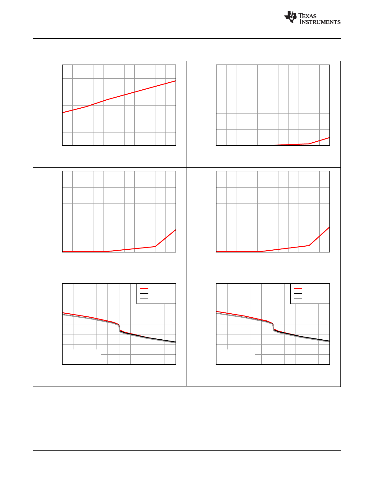
6.6 Typical Characteristics
Figure 1. VDD Supply Current vs. Junction Temperature Figure 2. VDD Shutdown Current vs. Junction Temperature
www.ti.com
Figure 3. VLDOIN Supply Current vs. Junction Temperature Figure 4. VLDOIN Shutdown Current vs. Junction
Figure 5. VTTREF Load Regulation (0.9 V) Figure 6. VTTREF Load Regulation (0.75 V)
6 Submit Documentation Feedback Copyright © 2011–2014, Texas Instruments Incorporated
Temperature
Product Folder Links: TPS51206
0.625
0.635
0.645
0.655
0.665
0.675
0.685
0.695
0.705
0.715
0.725
−1.5 −1.0 −0.5 0.0 0.5 1.0 1.5
VTT Current (A)
VTT Voltage (V)
TA = −40°C
TA = 25°C
TA = 85°C
V
VDDQSNS
= 1.35 V
V
VDD
= 5 V
0.550
0.560
0.570
0.580
0.590
0.600
0.610
0.620
0.630
0.640
0.650
−1.5 −1.0 −0.5 0.0 0.5 1.0 1.5
VTT Current (A)
VTT Voltage (V)
TA = −40°C
TA = 25°C
TA = 85°C
V
VDDQSNS
= 1.2 V
V
VDD
= 5 V
0.850
0.860
0.870
0.880
0.890
0.900
0.910
0.920
0.930
0.940
0.950
−2.0 −1.5 −1.0 −0.5 0.0 0.5 1.0 1.5 2.0
VTT Current (A)
VTT Voltage (V)
TA = −40°C
TA = 25°C
TA = 85°C
V
VDDQSNS
= 1.8 V
V
VDD
= 5 V
0.700
0.710
0.720
0.730
0.740
0.750
0.760
0.770
0.780
0.790
0.800
−2.0 −1.5 −1.0 −0.5 0.0 0.5 1.0 1.5 2.0
VTT Current (A)
VTT Voltage (V)
TA = −40°C
TA = 25°C
TA = 85°C
V
VDDQSNS
= 1.5 V
V
VDD
= 5 V
0.660
0.665
0.670
0.675
0.680
0.685
0.690
−10 −8 −6 −4 −2 0 2 4 6 8 10
VTTREF Current (mA)
VTTREF Voltage (V)
TA = −40°C
TA = 25°C
TA = 85°C
V
VDDQSNS
= 1.35 V
V
VDD
= 5 V
0.585
0.590
0.595
0.600
0.605
0.610
0.615
−10 −8 −6 −4 −2 0 2 4 6 8 10
VTTREF Current (mA)
VTTREF Voltage (V)
TA = −40°C
TA = 25°C
TA = 85°C
V
VDDQSNS
= 1.2 V
V
VDD
= 5 V
www.ti.com
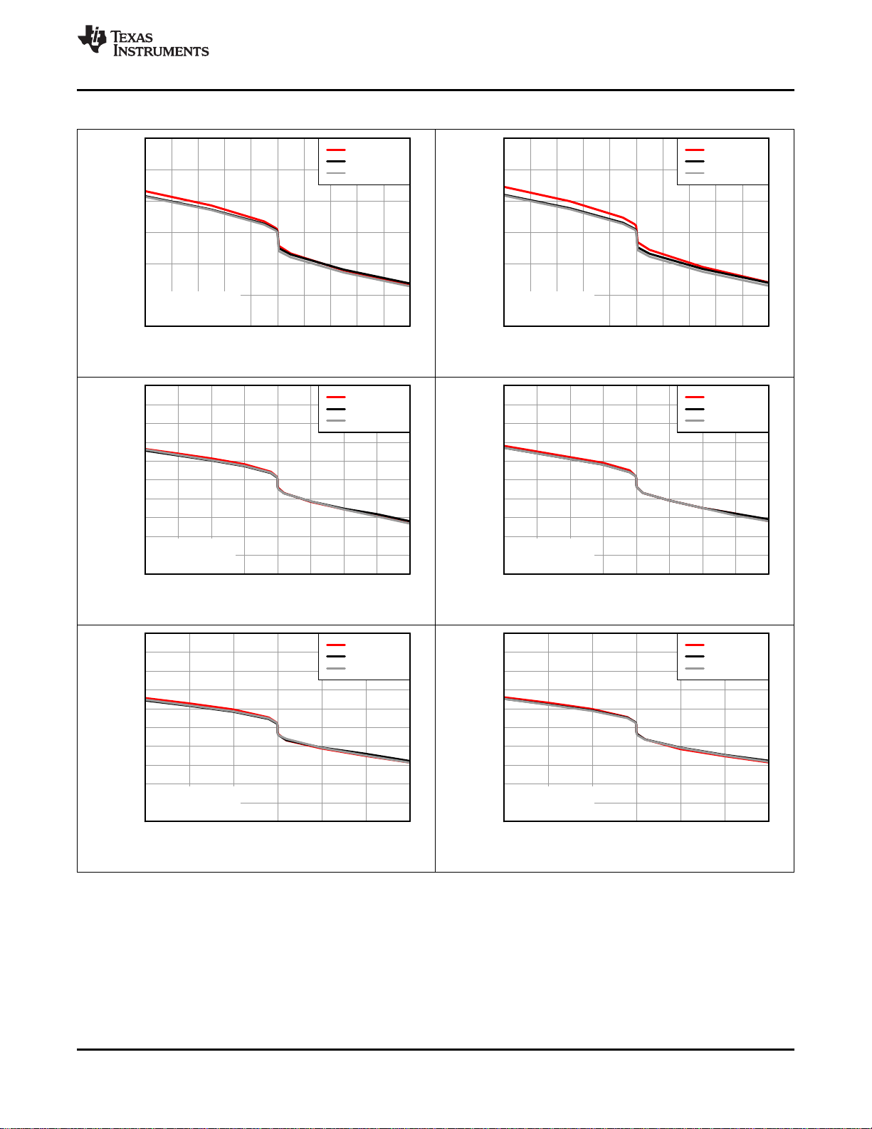
Typical Characteristics (continued)
Figure 7. VTTREF Load Regulation (0.675 V) Figure 8. VTTREF Load Regulation (0.6 V)
TPS51206
SLUSAH1B –MAY 2011–REVISED DECEMBER 2014
Figure 9. VTT Load Regulation (0.9 V) Figure 10. VTT Load Regulation (0.75 V)
Figure 11. VTT Load Regulation (0.675 V) Figure 12. VTT Load Regulation (0.6 V)
Copyright © 2011–2014, Texas Instruments Incorporated Submit Documentation Feedback 7
Product Folder Links: TPS51206
1000 10000 100000 1000000 10000000
−80
−60
−40
−20
0
20
40
60
80
−180
−135
−90
−45
0
45
90
135
180
Frequency (Hz)
Gain (dB)
Phase (°)
Gain
Phase
Sink: −1 A
V
VDD
= 5 V
V
VDDQSNS
= 1.5 V
1000 10000 100000 1000000 10000000
−80
−60
−40
−20
0
20
40
60
80
−180
−135
−90
−45
0
45
90
135
180
Frequency (Hz)
Gain (dB)
Phase (°)
Gain
Phase
Source: +1 A
V
VDD
= 5 V
V
VDDQSNS
= 1.5 V
I
VTT
(2 A/div)
V
VTTREF
(10 mV/div) 0.675 V offset
Time (200 ms/div)
V
VTT
(20 mV/div)
0.675 V offset
V
VDDQSNS
(50 mV/div)
1.35 V offset
I
VTT
(2 A/div)
V
VTTREF
(10 mV/div) 0.6 V offset
Time (200 ms/div)
V
VTT
(20 mV/div)
0.6 V offset
V
VDDQSNS
(50 mV/div)
1.2 V offset
I
VTT
(2 A/div)
V
VTTREF
(10 mV/div) 0.9 V offset
Time (200 ms/div)
V
VTT
(20 mV/div)
0.9 V offset
V
VDDQSNS
(50 mV/div)
1.8 V offset
I
VTT
(2 A/div)
V
VTTREF
(10 mV/div) 0.75 V offset
Time (200 ms/div)
V
VTT
(20 mV/div)
0.75 V offset
V
VDDQSNS
(50 mV/div)
1.5 V offset
TPS51206
SLUSAH1B –MAY 2011–REVISED DECEMBER 2014
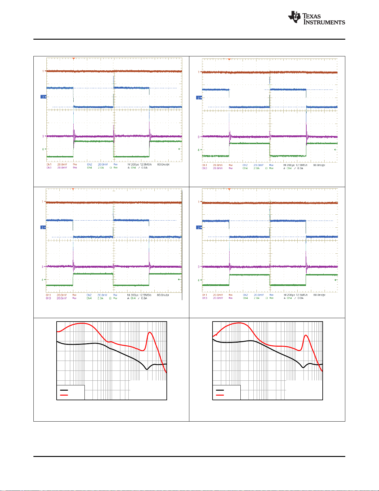
Typical Characteristics (continued)
www.ti.com
Figure 13. VTT Load Transient Response (0.9 V)
Figure 15. VTT Load Transient Response (0.675 V)
Figure 14. VTT Load Transient Response (0.75 V)
Figure 16. VTT Load Transient Response (0.6 V)
Figure 17. VTT (Sink: -1 A) Bode Plot (0.75 V) Figure 18. VTT (Source: +1 A) Bode Plot (0.75 V)
8 Submit Documentation Feedback Copyright © 2011–2014, Texas Instruments Incorporated
Product Folder Links: TPS51206
I
VTTREF
= 0 A
I
VTT
= 0 A
S3/S5: High to Low
V
VTTREF
(500 mV/div)
V
VTT
(500 mV/div)
VS5(5 V/div)
VS3(5 V/div)
Time (2 s/div)
0.00
0.05
0.10
0.15
0.20
0.25
0.30
0.0 0.5 1.0 1.5 2.0
VTT Current (A)
VTT Dropout Voltage (V)
V
OUT
= 0.900 V
V
OUT
= 0.750 V
V
OUT
= 0.675 V
V
OUT
= 0.600 V
TA = 25°C
V
VDD
= 5 V
V
VTTREF
(500 mV/div)
Time (40 ms/div)
V
VTT
(500 mV/div)
VS5(5 V/div)
VS3(5 V/div)
I
VTTREF
= 0 A
S5: Low to High
I
VTTREF
= 0 A
I
VTT
= 0 A
S3: Low to High
V
VTTREF
(500 mV/div)
V
VTT
(500 mV/div)
VS5(5 V/div)
VS3(5 V/div)
Time (1 ms/div)
www.ti.com
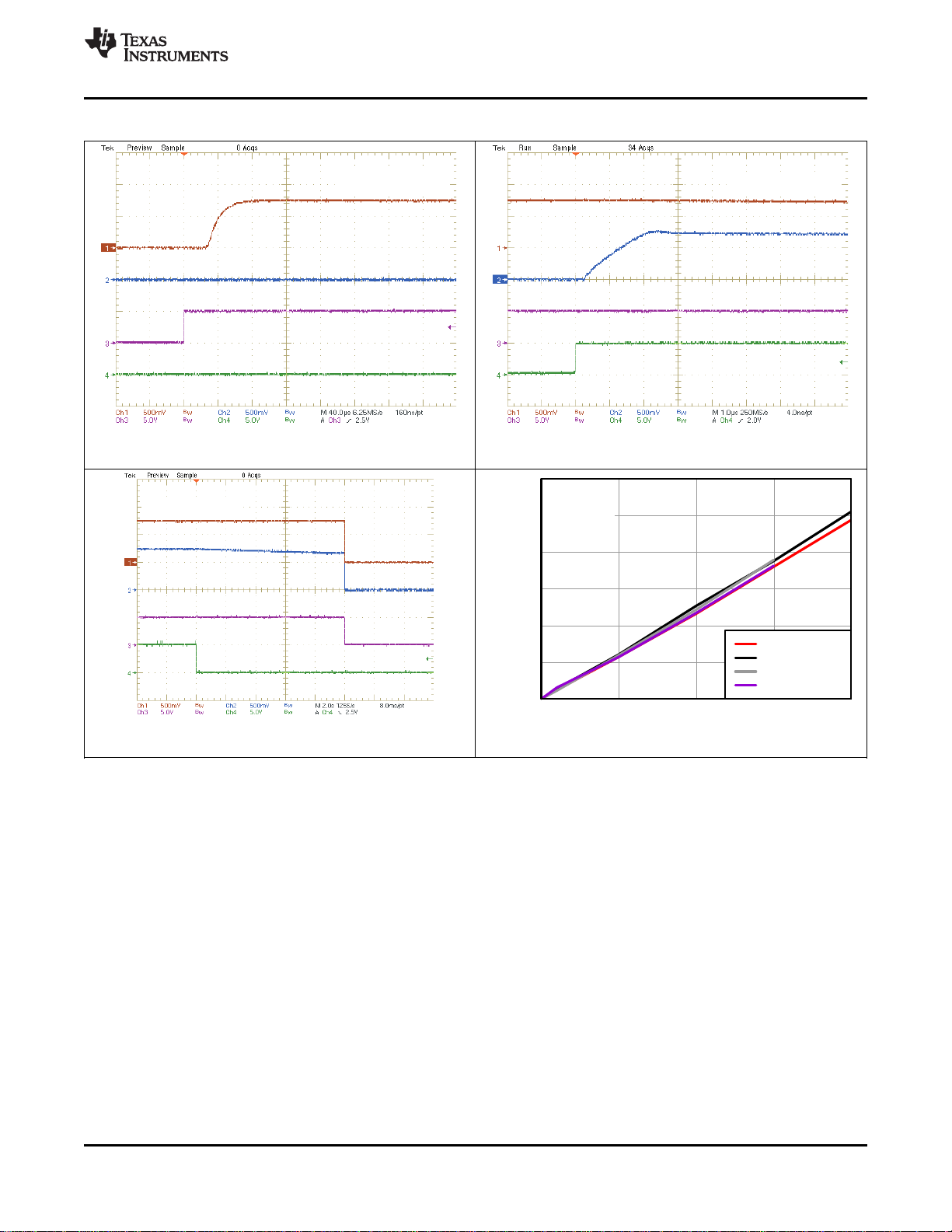
Typical Characteristics (continued)
Figure 19. Start-Up Waveforms (S5: Low to High) Figure 20. Start-Up Waveforms (S3: Low to High)
TPS51206
SLUSAH1B –MAY 2011–REVISED DECEMBER 2014
Figure 21. Shutdown Waveforms (S3/ S5: High to Low)
Copyright © 2011–2014, Texas Instruments Incorporated Submit Documentation Feedback 9
Figure 22. VTT Dropout Voltage
Product Folder Links: TPS51206

1
2
7
9
VTT
VTTSNS
PGND
VTTREF
VDDQSNS
VLDOIN
S3
S5
TPS51206
10VDD
GND
UDG-11025
+
3
5
4
6
8
+
+
+
OTP
GND
2.9V/2.7 V
+
+
GND
GND
OTP-OK
EN-VTTREF
EN-VTT
VTT Disharge
VTTREF Disharge
GND
TPS51206
SLUSAH1B –MAY 2011–REVISED DECEMBER 2014
www.ti.com
7 Detailed Description
7.1 Overview
The TPS51206 is a sink/source double date rate (DDR) termination regulator with VTTREF buffered reference
output.
7.2 Functional Block Diagram
7.3 Feature Description
7.3.1 VTT Sink and Source Regulator
The TPS51206 is a sink/source tracking termination regulator specifically designed for low input voltage, low
cost, and low external component count systems where space is a key application parameter. The TPS51206
integrates a high-performance, low-dropout (LDO) linear regulator (VTT) that has ultimate fast response to track
½ VDDQSNS within 40 mV at all conditions, and its current capability is 2 A for both sink and source directions.
A 10-µF (or greater) ceramic capacitor(s) need to be attached close to the VTT terminal for stable operation; X5R
or better grade is recommended. To achieve tight regulation with minimum effect of trace resistance, the remote
sensing terminal, VTTSNS, should be connected to the positive terminal of the output capacitor(s) as a separate
trace from the high current path from the VTT pin.
The TPS51206 has a dedicated pin, VLDOIN, for VTT power supply to minimize the LDO power dissipation on
user application. The minimum VLDOIN voltage is 0.4 V above the ½ VDDQSNS voltage.
7.3.2 VTTREF
The VTTREF pin includes 10 mA of sink/source current capability, and tracks ½ of VDDQSNS with ±1%
accuracy. A 0.22-µF ceramic capacitor needs to be attached close to the VTTREF terminal for stable operation;
X5R or better grade is recommended.
10 Submit Documentation Feedback Copyright © 2011–2014, Texas Instruments Incorporated
Product Folder Links: TPS51206

UDG-11136
VDD
VLDOIN
S5
S3
VTTREF
VTT
VDDQSNS
TPS51206
www.ti.com
SLUSAH1B –MAY 2011–REVISED DECEMBER 2014
Feature Description (continued)
7.3.3 VDD Undervoltage Lockout Protection
The TPS51206 input voltage (VDD) includes undervoltage lockout protection (UVLO). When the VDD pin voltage
is lower than UVLO threshold voltage, VTT and VTTREF are shut off. This is non-latch protection.
7.3.4 Overtemperature Protection
This device features internal temperature monitoring. If the temperature exceeds the threshold value, VTT and
VTTREF are shut off. This is a non-latch protection.
Figure 23. Typical Timing Diagram
7.4 Device Functional Modes
7.4.1 Power State Control
The TPS51206 has two input pins, S3 and S5, to provide simple control of the power state. Table 1 describes
S3/S5 terminal logic state and corresponding state of VTTREF/VTT outputs. VTT is turn-off and placed to high
impedance (High-Z) state in S3. The VTT output is floated and does not sink or source current in this state.
When both S5 and S3 pins are LOW, the power state is set to S4/S5. In S4/S5 state, all the outputs are turn-off
and discharged to GND.
Table 1. S3 and S5 Control Table
STATE S3 S5 VTTREF VTT
S0 HI HI ON ON
S3 LO HI ON OFF(High-Z)
S4/S5 LO LO OFF(Discharge) OFF(Discharge)
Copyright © 2011–2014, Texas Instruments Incorporated Submit Documentation Feedback 11
Product Folder Links: TPS51206

1
2
7
9
3
5
4
6
VTT
VTTSNS
PGND
VTTREF
VDDQSNS
VLDOIN
S3
S5
TPS51206
10 VDD 8GND
C3
10 mF
PowerPad
VTT
VTTREF
UDG-11026
C4
0.22 mF
C2
0.1 mF
C1
10 mF
VDDQ
S3_SLP
S5_SLP
5 V or 3.3 V
GND
TPS51206
SLUSAH1B –MAY 2011–REVISED DECEMBER 2014
www.ti.com
8 Application and Implementation
NOTE
Information in the following applications sections is not part of the TI component
specification, and TI does not warrant its accuracy or completeness. TI’s customers are
responsible for determining suitability of components for their purposes. Customers should
validate and test their design implementation to confirm system functionality.
8.1 Application Information
The TPS51206 is typically used as a sink and source tracking termination regulator which converts a voltage
from VTT+0.4 V to 3.5 V
8.2 Typical Applications
8.2.1 VLDOIN = VDDQ Configuration
Figure 24 shows an application diagram for a configuration where VLDOIN and VDDQ are connected.
Figure 24. VLDOIN = VDDQ Configuration
8.2.1.1 Design Requirements
Table 2. Design Parameters
PARAMETER EXAMPLE VALUE
Supply Voltage (VDD) 3.3 V or 5 V
8.2.1.2 Detailed Design Procedure
C1, C3 10 µF, 6.3 V, X5R, 1608 (0603) Taiyo Yuden JMK107BJ106MA
12 Submit Documentation Feedback Copyright © 2011–2014, Texas Instruments Incorporated
VLDOIN = VDDQ 1.5 V
REFERENCE PART
DESIGNATOR NUMBER
Output Current ±2 A
Table 3. VLDOIN = VDDQ Configuration Components
SPECIFICATION MANUFACTURER
Product Folder Links: TPS51206

3
5
4
VTT
VTTSNS
PGND
TPS51206
C3
10 mF
VTT
UDG-11137
C
C
R
C
TPS51206
www.ti.com
SLUSAH1B –MAY 2011–REVISED DECEMBER 2014
Table 3. VLDOIN = VDDQ Configuration Components (continued)
REFERENCE PART
DESIGNATOR NUMBER
C2 0.1 µF, 6.3 V, X5R, 1005 (0402) Taiyo Yuden JWK105BJ104MP
C4 0.22 µF, 6.3 V, X5R, 1005 (0402) Taiyo Yuden JMK105BJ224KV
8.2.1.2.1 VDD Capacitor
SPECIFICATION MANUFACTURER
Add a ceramic capacitor, with a value 0.1 µF (or greater) and X5R grade (or better), placed close to the VDD
terminal, to stabilize the bias supply voltage from any parasitic impedance from the power supply rail.
8.2.1.2.2 VLDOIN Capacitor
Depending on the trace impedance between the VLDOIN bulk power supply to the device, a transient increase of
source current is supplied mostly by the charge from the VLDOIN input capacitor. Use a 10-µF (or greater) and
X5R grade (or better) ceramic capacitor to supply this transient charge.
8.2.1.2.3 VTTREF Capacitor
Add a ceramic capacitor, with a value 0.22 µF and X5R grade (or better), placed close to the VTTREF terminal
for stable operation.
8.2.1.2.4 VTT Capacitor
For stable operation, a 10-µF (or greater) and X5R (or better) grade ceramic capacitor(s) need to be attached
close to the VTT terminal. This capacitor is recommended to minimize any additional equivalent series resistance
(ESR) and/or equivalent series inductance (ESL) of ground trace between the PGND terminal and the VTT
capacitor(s).
8.2.1.2.5 VTTSNS Connection
To achieve tight regulation with minimum effect of trace resistance, a remote sensing terminal, the VTTSNS pin
should be connected to the positive terminal of the VTT pin output capacitor(s) as a separate trace from the highcurrent path from VTT. Consider adding a low-pass R-C filter at the VTTSNS pin in case the ESR of the VTT
output capacitor(s) is larger than 2 mΩ. The R-C filter time constant should be approximately the same or slightly
lower than the time constant of the VTT output capacitance and ESR.
Figure 25. R-C Filter for VTTSNS
8.2.1.2.6 VDDQSNS Connection
VDDQSNS is a reference input of the VTTREF and VTT. Trace should be routed away from noise-generating
lines.
Copyright © 2011–2014, Texas Instruments Incorporated Submit Documentation Feedback 13
Product Folder Links: TPS51206

1
2
7
9
3
5
4
6
VTT
VTTSNS
PGND
VTTREF
VDDQSNS
VLDOIN
S3
S5
TPS51206
10 VDD 8GND
C3
10 mF
PowerPad
VTT
VTTREF
UDG-11027
C4
0.22 mF
C2
0.1 mF
C1
10 mF
VTT Power
S3_SLP
S5_SLP
5 V or 3.3 V
Supply
GND
VDDQ Sense
I
VTT
(2 A/div)
V
VTTREF
(10 mV/div) 0.75 V offset
Time (200 ms/div)
V
VTT
(20 mV/div)
0.75 V offset
V
VDDQSNS
(50 mV/div)
1.5 V offset
TPS51206
SLUSAH1B –MAY 2011–REVISED DECEMBER 2014
8.2.1.3 Application Curves
Figure 26. VTT Load Transient Response (0.75 V)
www.ti.com
8.2.2 VLDOIN Separated from VDDQ Configuration
Figure 27 shows an application diagram for a configuration where VLDOIN and VDDQ are separated.
Figure 27. VLDOIN Separated from VDDQ Configuration
Product Folder Links: TPS51206
14 Submit Documentation Feedback Copyright © 2011–2014, Texas Instruments Incorporated

I
VTTREF
= 0 A
I
VTT
= 0 A
S3: Low to High
V
VTTREF
(500 mV/div)
V
VTT
(500 mV/div)
VS5(5 V/div)
VS3(5 V/div)
Time (1 ms/div)
I
VTTREF
= 0 A
I
VTT
= 0 A
S3/S5: High to Low
V
VTTREF
(500 mV/div)
V
VTT
(500 mV/div)
VS5(5 V/div)
VS3(5 V/div)
Time (2 s/div)
www.ti.com
8.2.2.1 Design Requirements
PARAMETER EXAMPLE VALUE
Supply Voltage (VDD)
VLDOIN = VDDQ
Output Current
8.2.2.2 Detailed Design Procedure
Table 5. VLDOIN Separated from VDDQ Configuration Components
REFERENCE PART
DESIGNATOR NUMBER
C1, C3 10 µF, 6.3V, X5R, 1608 (0603) Taiyo Yuden JMK107BJ106MA
C2 0.1 µF, 6.3V, X5R, 1005 (0402) Taiyo Yuden JWK105BJ104MP
C3 10 µF, 6.3V, X5R, 1608 (0603) Taiyo Yuden JMK107BJ106MA
C4 0.22 µF, 6.3V, X5R, 1005 (0402) Taiyo Yuden JMK105BJ224KV
8.2.2.3 Application Curves
TPS51206
SLUSAH1B –MAY 2011–REVISED DECEMBER 2014
Table 4. Design Parameters
3.3 V or 5 V
1.5 V
±2 A
SPECIFICATION MANUFACTURER
Copyright © 2011–2014, Texas Instruments Incorporated Submit Documentation Feedback 15
Figure 28. Start-Up Waveforms (S3: Low to High) Figure 29. Shutdown Waveforms (S3 / S5: High to Low)
Product Folder Links: TPS51206

TPS51206
SLUSAH1B –MAY 2011–REVISED DECEMBER 2014
www.ti.com
9 Power Supply Recommendations
TPS51206 is designed for a sink / source double date rate (DDR) termination regulator with VTTREF buffered
reference output. Supply input voltage (VDD) supports 3.3-V rail and 5-V rail; VLDOIN input voltage supports
VTT+0.4 V to 3.5 V.
10 Layout
10.1 Layout Guidelines
Consider the following before beginning a TPS51206 layout design.
• The input bypass capacitor for VLDOIN should be placed as close as possible to the terminal with short and
wide connections.
• The output capacitor for VTT should be placed close to the terminals (VTT and PGND) with short and wide
connection in order to avoid additional ESR and/or ESL trace inductance.
• VTTSNS should be connected to the positive node of VTT output capacitor(s) as a separate trace from the
high current VTT power trace. In addition, VTTSNS trace should be routed away from high current trace, on
the separate layer is recommended. This configuration is strongly recommended to avoid additional ESR
and/or ESL. If sensing the voltage at the point of the load is required, it is recommended to attach the output
capacitor(s) at that point. In addition, it is recommended to minimize any additional ESR and/or ESL of ground
trace between the GND pin and the VTT capacitor(s).
• The GND pin (and the negative node of the VTTREF output capacitor) and PGND pins (and the negative
node of the VTT output capacitor) should be connected to the internal system ground planes (for better result,
use at least two internal ground planes) with multiple vias. Use as many vias as possible to reduce the
impedance between GND/PGND and the system ground plane.
• In order to effectively remove heat from the package, properly prepare the thermal land. Apply solder directly
to the package thermal pad. The wide traces of the component and the side copper connected to the thermal
land pad help to dissipate heat. Numerous vias 0.33 mm in diameter connected from the thermal land to the
internal/solder side ground plane(s) should also be used to help dissipation. Please consult the TPS51206-
EVM User's Guide for more detailed layout recommendations.
16 Submit Documentation Feedback Copyright © 2011–2014, Texas Instruments Incorporated
Product Folder Links: TPS51206

-
=
q
J(max) A(max)
PKG
JA
T T
P
= ´
DISS(snk ) VTT VTT(snk )
P V I
( )
= - ´
DISS(src ) VLDOIN VTT VTT(src)
P V V I
UDG-11135
0.22 mF
0402
0.1 mF
0402
VLDOIN
VTT
PGND
VTTSNS
VDD
S5
GND
S3
VTTREF
VDDQSNS
Via to Ground Plane
Via for VTTSNS
VTTREFOutput
5-V or 3.3-V Supply Input
VTT Output
VDDQ Sense Input
VTT Power
Supply Input
Etch Beneath Component
10 mF
0603
10 mF
0603
www.ti.com
10.2 Layout Example
TPS51206
SLUSAH1B –MAY 2011–REVISED DECEMBER 2014
Figure 30. PCB Layout Guideline
10.3 Thermal Considerations
Because the TPS51206 is a linear regulator, the VTT current flows in both source and sink directions, thereby
dissipating power from the device. When the device is sourcing current, the voltage difference between VLDOIN
and VTT times I
In this case, if the VLDOIN pin is connected to an alternative power supply lower than the VDDQ voltage, overall
power loss can be reduced. For the sink phase, VTT voltage is applied across the internal LDO regulator, and
the power dissipation can be calculated by Equation 2.
Maximum power dissipation allowed by the package is calculated by Equation 3.
where
(VTT current) current becomes the power dissipation as shown in Equation 1.
VTT
• T
• T
is 125°C
J(max)
is the maximum ambient temperature in the system
A(max)
• θJAis the thermal resistance from junction to ambient (3)
(1)
(2)
Copyright © 2011–2014, Texas Instruments Incorporated Submit Documentation Feedback 17
Product Folder Links: TPS51206

TPS51206
SLUSAH1B –MAY 2011–REVISED DECEMBER 2014
www.ti.com
11 Device and Documentation Support
11.1 Device Support
11.1.1 Third-Party Products Disclaimer
TI'S PUBLICATION OF INFORMATION REGARDING THIRD-PARTY PRODUCTS OR SERVICES DOES NOT
CONSTITUTE AN ENDORSEMENT REGARDING THE SUITABILITY OF SUCH PRODUCTS OR SERVICES
OR A WARRANTY, REPRESENTATION OR ENDORSEMENT OF SUCH PRODUCTS OR SERVICES, EITHER
ALONE OR IN COMBINATION WITH ANY TI PRODUCT OR SERVICE.
11.2 Trademarks
PowerPAD is a trademark of Texas Instruments.
All other trademarks are the property of their respective owners.
11.3 Electrostatic Discharge Caution
These devices have limited built-in ESD protection. The leads should be shorted together or the device placed in conductive foam
during storage or handling to prevent electrostatic damage to the MOS gates.
11.4 Glossary
SLYZ022 — TI Glossary.
This glossary lists and explains terms, acronyms, and definitions.
12 Mechanical, Packaging, and Orderable Information
The following pages include mechanical, packaging, and orderable information. This information is the most
current data available for the designated devices. This data is subject to change without notice and revision of
this document. For browser-based versions of this data sheet, refer to the left-hand navigation.
18 Submit Documentation Feedback Copyright © 2011–2014, Texas Instruments Incorporated
Product Folder Links: TPS51206

PACKAGE OPTION ADDENDUM
www.ti.com
27-Oct-2014
PACKAGING INFORMATION
Orderable Device Status
TPS51206DSQR ACTIVE SON DSQ 10 3000 Green (RoHS
TPS51206DSQT ACTIVE SON DSQ 10 250 Green (RoHS
(1)
The marketing status values are defined as follows:
ACTIVE: Product device recommended for new designs.
LIFEBUY: TI has announced that the device will be discontinued, and a lifetime-buy period is in effect.
NRND: Not recommended for new designs. Device is in production to support existing customers, but TI does not recommend using this part in a new design.
PREVIEW: Device has been announced but is not in production. Samples may or may not be available.
OBSOLETE: TI has discontinued the production of the device.
Package Type Package
(1)
Drawing
Pins Package
Qty
Eco Plan
(2)
& no Sb/Br)
& no Sb/Br)
Lead/Ball Finish
(6)
CU NIPDAU Level-2-260C-1 YEAR -40 to 85 1206
CU NIPDAU Level-2-260C-1 YEAR -40 to 85 1206
MSL Peak Temp
(3)
Op Temp (°C) Device Marking
(4/5)
(2)
Eco Plan - The planned eco-friendly classification: Pb-Free (RoHS), Pb-Free (RoHS Exempt), or Green (RoHS & no Sb/Br) - please check http://www.ti.com/productcontent for the latest availability
information and additional product content details.
TBD: The Pb-Free/Green conversion plan has not been defined.
Pb-Free (RoHS): TI's terms "Lead-Free" or "Pb-Free" mean semiconductor products that are compatible with the current RoHS requirements for all 6 substances, including the requirement that
lead not exceed 0.1% by weight in homogeneous materials. Where designed to be soldered at high temperatures, TI Pb-Free products are suitable for use in specified lead-free processes.
Pb-Free (RoHS Exempt): This component has a RoHS exemption for either 1) lead-based flip-chip solder bumps used between the die and package, or 2) lead-based die adhesive used between
the die and leadframe. The component is otherwise considered Pb-Free (RoHS compatible) as defined above.
Green (RoHS & no Sb/Br): TI defines "Green" to mean Pb-Free (RoHS compatible), and free of Bromine (Br) and Antimony (Sb) based flame retardants (Br or Sb do not exceed 0.1% by weight
in homogeneous material)
(3)
MSL, Peak Temp. - The Moisture Sensitivity Level rating according to the JEDEC industry standard classifications, and peak solder temperature.
(4)
There may be additional marking, which relates to the logo, the lot trace code information, or the environmental category on the device.
(5)
Multiple Device Markings will be inside parentheses. Only one Device Marking contained in parentheses and separated by a "~" will appear on a device. If a line is indented then it is a continuation
of the previous line and the two combined represent the entire Device Marking for that device.
(6)
Lead/Ball Finish - Orderable Devices may have multiple material finish options. Finish options are separated by a vertical ruled line. Lead/Ball Finish values may wrap to two lines if the finish
value exceeds the maximum column width.
Important Information and Disclaimer:The information provided on this page represents TI's knowledge and belief as of the date that it is provided. TI bases its knowledge and belief on information
provided by third parties, and makes no representation or warranty as to the accuracy of such information. Efforts are underway to better integrate information from third parties. TI has taken and
continues to take reasonable steps to provide representative and accurate information but may not have conducted destructive testing or chemical analysis on incoming materials and chemicals.
TI and TI suppliers consider certain information to be proprietary, and thus CAS numbers and other limited information may not be available for release.
Samples
Addendum-Page 1

PACKAGE OPTION ADDENDUM
www.ti.com
In no event shall TI's liability arising out of such information exceed the total purchase price of the TI part(s) at issue in this document sold by TI to Customer on an annual basis.
27-Oct-2014
Addendum-Page 2

PACKAGE MATERIALS INFORMATION
www.ti.com 27-Oct-2014
TAPE AND REEL INFORMATION
*All dimensions are nominal
Device Package
TPS51206DSQR SON DSQ 10 3000 180.0 8.4 2.3 2.3 1.15 4.0 8.0 Q2
TPS51206DSQR SON DSQ 10 3000 180.0 8.4 2.3 2.3 1.15 4.0 8.0 Q2
TPS51206DSQT SON DSQ 10 250 180.0 8.4 2.3 2.3 1.15 4.0 8.0 Q2
Type
Package
Drawing
Pins SPQ Reel
Diameter
(mm)
Reel
Width
W1 (mm)
A0
(mm)B0(mm)K0(mm)P1(mm)W(mm)
Pin1
Quadrant
Pack Materials-Page 1

PACKAGE MATERIALS INFORMATION
www.ti.com 27-Oct-2014
*All dimensions are nominal
Device Package Type Package Drawing Pins SPQ Length (mm) Width (mm) Height (mm)
TPS51206DSQR SON DSQ 10 3000 210.0 185.0 35.0
TPS51206DSQR SON DSQ 10 3000 210.0 185.0 35.0
TPS51206DSQT SON DSQ 10 250 210.0 185.0 35.0
Pack Materials-Page 2


IMPORTANT NOTICE
Texas Instruments Incorporated and its subsidiaries (TI) reserve the right to make corrections, enhancements, improvements and other
changes to its semiconductor products and services per JESD46, latest issue, and to discontinue any product or service per JESD48, latest
issue. Buyers should obtain the latest relevant information before placing orders and should verify that such information is current and
complete. All semiconductor products (also referred to herein as “components”) are sold subject to TI’s terms and conditions of sale
supplied at the time of order acknowledgment.
TI warrants performance of its components to the specifications applicable at the time of sale, in accordance with the warranty in TI’s terms
and conditions of sale of semiconductor products. Testing and other quality control techniques are used to the extent TI deems necessary
to support this warranty. Except where mandated by applicable law, testing of all parameters of each component is not necessarily
performed.
TI assumes no liability for applications assistance or the design of Buyers’ products. Buyers are responsible for their products and
applications using TI components. To minimize the risks associated with Buyers’ products and applications, Buyers should provide
adequate design and operating safeguards.
TI does not warrant or represent that any license, either express or implied, is granted under any patent right, copyright, mask work right, or
other intellectual property right relating to any combination, machine, or process in which TI components or services are used. Information
published by TI regarding third-party products or services does not constitute a license to use such products or services or a warranty or
endorsement thereof. Use of such information may require a license from a third party under the patents or other intellectual property of the
third party, or a license from TI under the patents or other intellectual property of TI.
Reproduction of significant portions of TI information in TI data books or data sheets is permissible only if reproduction is without alteration
and is accompanied by all associated warranties, conditions, limitations, and notices. TI is not responsible or liable for such altered
documentation. Information of third parties may be subject to additional restrictions.
Resale of TI components or services with statements different from or beyond the parameters stated by TI for that component or service
voids all express and any implied warranties for the associated TI component or service and is an unfair and deceptive business practice.
TI is not responsible or liable for any such statements.
Buyer acknowledges and agrees that it is solely responsible for compliance with all legal, regulatory and safety-related requirements
concerning its products, and any use of TI components in its applications, notwithstanding any applications-related information or support
that may be provided by TI. Buyer represents and agrees that it has all the necessary expertise to create and implement safeguards which
anticipate dangerous consequences of failures, monitor failures and their consequences, lessen the likelihood of failures that might cause
harm and take appropriate remedial actions. Buyer will fully indemnify TI and its representatives against any damages arising out of the use
of any TI components in safety-critical applications.
In some cases, TI components may be promoted specifically to facilitate safety-related applications. With such components, TI’s goal is to
help enable customers to design and create their own end-product solutions that meet applicable functional safety standards and
requirements. Nonetheless, such components are subject to these terms.
No TI components are authorized for use in FDA Class III (or similar life-critical medical equipment) unless authorized officers of the parties
have executed a special agreement specifically governing such use.
Only those TI components which TI has specifically designated as military grade or “enhanced plastic” are designed and intended for use in
military/aerospace applications or environments. Buyer acknowledges and agrees that any military or aerospace use of TI components
which have not been so designated is solely at the Buyer's risk, and that Buyer is solely responsible for compliance with all legal and
regulatory requirements in connection with such use.
TI has specifically designated certain components as meeting ISO/TS16949 requirements, mainly for automotive use. In any case of use of
non-designated products, TI will not be responsible for any failure to meet ISO/TS16949.
Products Applications
Audio www.ti.com/audio Automotive and Transportation www.ti.com/automotive
Amplifiers amplifier.ti.com Communications and Telecom www.ti.com/communications
Data Converters dataconverter.ti.com Computers and Peripherals www.ti.com/computers
DLP® Products www.dlp.com Consumer Electronics www.ti.com/consumer-apps
DSP dsp.ti.com Energy and Lighting www.ti.com/energy
Clocks and Timers www.ti.com/clocks Industrial www.ti.com/industrial
Interface interface.ti.com Medical www.ti.com/medical
Logic logic.ti.com Security www.ti.com/security
Power Mgmt power.ti.com Space, Avionics and Defense www.ti.com/space-avionics-defense
Microcontrollers microcontroller.ti.com Video and Imaging www.ti.com/video
RFID www.ti-rfid.com
OMAP Applications Processors www.ti.com/omap TI E2E Community e2e.ti.com
Wireless Connectivity www.ti.com/wirelessconnectivity
Mailing Address: Texas Instruments, Post Office Box 655303, Dallas, Texas 75265
Copyright © 2014, Texas Instruments Incorporated

 Loading...