

Texas Instruments TPS51125A Datasheet
TPS51125A
www.ti.com
SLUS976F –SEPTEMBER 2009–REVISED SEPTEMBER 2012
Dual-Synchronous, Step-Down Controller with Out-of-Audio™ Operation
and 100-mA LDOs for Notebook System Power
Check for Samples: TPS51125A
1
FEATURES
2
• Wide Input Voltage Range: 5.5 V to 28 V
• Output Voltage Range: 2 V to 5.5 V • I/O Supplies
• Built-in 100-mA 5-V/3.3-V LDO with Switches • System Power Supplies
• Built-in 1% 2-V Reference Output
• With/Without Out-of-Audio™ Mode Selectable
Light Load and PWM only Operation
• Internal 1.6-ms Voltage Servo Softstart
• Adaptive On-Time Control Architecture with
Four Selectable Frequency Setting
• 4500 ppm/°C R
• Built-In Output Discharge
• Power Good Output
• Built-in OVP/UVP/OCP
• Thermal Shutdown (Non-latch)
• QFN24 (RGE)
Current Sensing
DS(on)
APPLICATIONS
• Notebook Computers
DESCRIPTION
The TPS51125A is a cost effective, dual-synchronous
buck controller targeted for notebook system power
supply solutions. It provides 5-V and 3.3-V LDOs and
requires few external components. The 270-kHz
VCLK output can be used to drive an external charge
pump, generating gate drive voltage for the load
switches without reducing the main converter’s
efficiency. The TPS51125A supports high efficiency,
fast transient response and provides a combined
power-good signal. Out-of-Audio™ mode light-load
operation enables low acoustic noise at much higher
efficiency than conventional forced PWM operation.
Adaptive on-time D-CAP™ control provides
convenient and efficient operation. The part operates
with supply input voltages ranging from 5.5 V to 28 V
and supports output voltages from 2 V to 5.5 V. The
TPS51125A is available in a 24-pin QFN package
and is specified from -40°C to 85°C ambient
temperature range.
Table 1. Differences between the TPS51125 and TPS51125A
LDO Output Capacitance Requirement
1
Please be aware that an important notice concerning availability, standard warranty, and use in critical applications of
Texas Instruments semiconductor products and disclaimers thereto appears at the end of this data sheet.
2Out-of-Audio, D-CAP are trademarks of Texas Instruments.
PRODUCTION DATA information is current as of publication date.
Products conform to specifications per the terms of the Texas
Instruments standard warranty. Production processing does not
necessarily include testing of all parameters.
(1 µF acceptable at no load) (1 µF acceptable at no load)
TPS51125 TPS51125A
VREG5: at least 33 µF VREG5: 10 µF or larger (X5R or X7R)
VREG3: at most 10 µF VREG3: 10 µF or larger (X5R or X7R)
VREF: 0.22 µF to 1 µF VREF: 0.22 µF to 1 µF (X5R or X7R)
Copyright © 2009–2012, Texas Instruments Incorporated
TPS51125A
SLUS976F –SEPTEMBER 2009–REVISED SEPTEMBER 2012
ORDERING INFORMATION
T
A
-40°C to 85°C 24
PACKAGE DEVICE NUMBER PINS OUTPUT SUPPLY ECO PLAN
Plastic Quad Flat Green (RoHS and no
Pack (QFN) Sb/Br)
TPS51125ARGET 250
TPS51125ARGER 3000
(1)(2)
MINIMUM
QUANTITY
Tape and reel
(small)
Tape and reel
(large)
www.ti.com
(1) For the most current package and ordering information, see the Package Option Addendum at the end of this document, or visit the TI
website at www.ti.com.
(2) Package drawings, standard packing quantities, thermal data, symbolization, and PCB design guidelines are available at
www.ti.com/sc/package
ABSOLUTE MAXIMUM RATINGS
(1)
over operating free-air temperature range (unless otherwise noted)
PARAMETER UNIT
VBST1, VBST2 –0.3 36
VIN –0.3 30
LL1, LL2 -2.0 30
Input voltage range
(1)
LL1, LL2, pulse width < 20 ns -5.0 30
VBST1, VBST2
(2)
EN0, ENTRIP1, ENTRIP2, VFB1, VFB2, VO1, VO2, TONSEL, SKIPSEL –0.3 6
DRVH1, DRVH2 -1.0 36
Output voltage range
(1)
DRVH1, DRVH2
(2)
PGOOD, VCLK, VREG3, VREG5, VREF, DRVL1, DRVL2 –0.3 6
Electrostatic discharge kV
T
J
T
stg
Human body model (HBM) QSS 009-105 (JESD22-A114A) 2
Charged device model (CDM) QSS 009-147 (JESD22-C101B.01) 1.5
Junction temperature range –40 125
Storage temperature –55 150
(1) Stresses beyond those listed under "absolute maximum ratings" may cause permanent damage to the device. These are stress ratings
only and functional operation of the device at these or any other conditions beyond those indicated under "recommended operating
conditions" is not implied. Exposure to absolute-maximum-rated conditions for extended periods may affect device reliability.
(2) Voltage values are with respect to the corresponding LLx terminal.
VALUE
MIN MAX
–0.3 6 V
–0.3 6
°C
DISSIPATION RATINGS
2-oz. trace and copper pad with solder.
PACKAGE TA< 25°C POWER RATING TA= 85°C POWER RATING
24 pin RGE
(1)
1.85 W 18.5 mW/°C 0.74 W
DERATING FACTOR ABOVE T
= 25°C
(1) Enhanced thermal conductance by 3x3 thermal vias beneath thermal pad.
2 Submit Documentation Feedback Copyright © 2009–2012, Texas Instruments Incorporated
Product Folder Links: TPS51125A
A
TPS51125A
www.ti.com
SLUS976F –SEPTEMBER 2009–REVISED SEPTEMBER 2012
RECOMMENDED OPERATING CONDITIONS
over operating free-air temperature range (unless otherwise noted)
PARAMETER MIN TYP MAX UNIT
Supply voltage VIN 5.5 28
VBST1, VBST2 -0.1 34
Input voltage range
Output voltage range LL1, LL2 -1.8 28
T
A
VBST1, VBST2 (wrt LLx) -0.1 5.5
EN0, ENTRIP1, ENTRIP2, VFB1, VFB2, VO1, VO2,
TONSEL, SKIPSEL
DRVH1, DRVH2 -0.8 34
DRVH1, DRVH2 (wrt LLx) -0.1 5.5
VREF, VREG3, VREG5 -0.1 5.5
PGOOD, VCLK, DRVL1, DRVL2 -0.1 5.5
Operating free-air temperature -40 85 °C
-0.1 5.5
V
Copyright © 2009–2012, Texas Instruments Incorporated Submit Documentation Feedback 3
Product Folder Links: TPS51125A
TPS51125A
SLUS976F –SEPTEMBER 2009–REVISED SEPTEMBER 2012
ELECTRICAL CHARACTERISTICS
over operating free-air temperature range, VIN = 12 V (unless otherwise noted)
PARAMETER CONDITIONS MIN TYP MAX UNIT
SUPPLY CURRENT
I
VIN1
I
VIN2
I
VO1
I
VO2
I
VINSTBY
I
VINSDN
VIN supply current1 = 0 V, EN0=open, ENTRIPx = 5 V, 0.55 1 mA
VIN supply current2 3.3 V, EN0=open, ENTRIPx = 5 V, 4 6.5 μA
VO1 current = 3.3 V, EN0=open, ENTRIPx = 5 V, 0.8 1.5 mA
VO2 current = 3.3 V, EN0=open, ENTRIPx = 5 V, 12 100
VIN standby current 95 150
VIN shutdown current 10 25
VREF OUTPUT
V
VREF
VREF output voltage V
VREG5 OUTPUT
V
VREG5
I
VREG5
V
TH5VSW
R
5VSW
VREG5 output voltage VO1 = 0 V, I
VREG5 output current VO1 = 0 V, VREG5 = 4.5 V 100 175 250 mA
Switch over threshold V
5 V SW R
ON
VREG3 OUTPUT
V
VREG3
I
VREG3
V
TH3VSW
R
3VSW
VREG3 output voltage VO2 = 0 V, I
VREG3 output current VO2 = 0 V, VREG3 = 3 V 100 175 250 mA
Switch over threshold V
3 V SW R
ON
INTERNAL REFERENCE VOLTAGE
V
V
I
IREF
VFB
VFB
Internal reference voltage I
VFB regulation voltage FB voltage, I
VFB input current VFBx = 2.0 V, TA= 25°C -20 20 nA
(1) Ensured by design. Not production tested.
VIN current, TA= 25°C, no load, VO1 = 0 V, VO2
VFB1 = VFB2 = 2.05 V
VIN current, TA= 25°C, no load, VO1 = 5 V, VO2 =
VFB1 = VFB2 = 2.05 V
VO1 current, TA= 25°C, no load, VO1 = 5 V, VO2
VFB1 = VFB2 = 2.05 V
VO2 current, TA= 25°C, no load, VO1 = 5 V, VO2
VFB1 = VFB2 = 2.05 V
VIN current, TA= 25°C, no load, μA
EN0 = 1.2 V, ENTRIPx = 0 V
VIN current, TA= 25°C, no load,
EN0 = ENTRIPx = 0 V
I
= 0 A 1.98 2.00 2.02
VREF
-5 μA < I
VO1 = 0 V, I
VO1 = 0 V, I
< 100 μA 1.97 2.00 2.03
VREF
< 100 mA, TA= 25°C 4.8 5 5.2
VREG5
< 100 mA, 6.5 V < VIN < 28 V 4.75 5 5.25 V
VREG5
< 50 mA, 5.5 V < VIN < 28 V 4. 75 5 5.25
VREG5
Turns on 4.55 4.7 4.85
Hysteresis 0.15 0.25 0.3
VO1 = 5 V, I
VO2 = 0 V, I
VO2 = 0 V, I
= 100 mA 1 3 Ω
VREG5
< 100 mA, TA= 25°C 3.2 3.33 3.46
VREG3
< 100 mA, 6.5 V < VIN < 28 V 3.13 3.33 3.5 V
VREG3
< 50 mA, 5.5 V < VIN < 28 V 3.13 3.33 3.5
VREG3
Turns on 3.05 3.15 3.25
Hysteresis 0.1 0.2 0.25
VO2 = 3.3 V, I
= 0 A, beginning of ON state 1.95 1.98 2.01
VREF
FB voltage, I
FB voltage, I
= 100 mA 1.5 4 Ω
VREG3
= 0 A, skip mode 1.98 2.01 2.04
VREF
= 0 A, OOA mode
VREF
= 0 A, continuous conduction
VREF
(1)
www.ti.com
2.00 2.035 2.07
(1)
2.00
V
4 Submit Documentation Feedback Copyright © 2009–2012, Texas Instruments Incorporated
Product Folder Links: TPS51125A

TPS51125A
www.ti.com
SLUS976F –SEPTEMBER 2009–REVISED SEPTEMBER 2012
ELECTRICAL CHARACTERISTICS (continued)
over operating free-air temperature range, VIN = 12 V (unless otherwise noted)
PARAMETER CONDITIONS MIN TYP MAX UNIT
V
DISCHARGE
OUT
I
Dischg
OUTPUT DRIVERS
R
DRVH
R
DRVL
t
D
CLOCK OUTPUT
V
CLKH
V
CLKL
f
CLK
INTERNAL BST DIODE
V
FBST
I
VBSTLK
DUTY AND FREQUENCY CONTROL
t
ON11
t
ON12
t
ON13
t
ON14
t
ON21
t
ON22
t
ON23
t
ON24
t
ON(min)
t
OFF(min)
SOFT-START
t
SS
POWERGOOD
V
THPG
I
PGMAX
t
PGDEL
VOUT discharge current ENTRIPx = 0 V, VOx = 0.5 V 10 60 mA
DRVH resistance
DRVL resistance
Dead time ns
High level voltage I
Low level voltage I
Source, V
Sink, V
Source, V
Sink, V
DRVHx-off to DRVLx-on 10
DRVLx-off to DRVHx-on 30
VCLK
VCLK
BSTx - DRVHx
DRVHx - LLx
VREG5 - DRVLx
= 100 mV 1.5 4
DRVLx
= -10 mA, VO1 = 5 V, TA= 25 °C 4.84 4.92
= 10 mA, VO1 = 5 V, TA= 25 °C 0.06 0.12
= 100 mV 4 8
= 100 mV 1.5 4
= 100 mV 4 8
Clock frequency TA= 25 °C 175 270 325 kHz
Forward voltage V
VREG5-VBSTx
, IF= 10 mA, TA= 25 °C 0.7 0.8 0.9 V
VBST leakage current VBSTx = 34 V, LLx = 28 V, TA= 25 °C 0.1 1 μA
CH1 on time 1 VIN= 12 V, VO1 = 5 V, 200 kHz setting 2080
CH1 on time 2 VIN= 12 V, VO1 = 5 V, 245 kHz setting 1700
CH1 on time 3 VIN= 12 V, VO1 = 5 V, 300 kHz setting 1390
CH1 on time 4 VIN= 12 V, VO1 = 5 V, 365 kHz setting 1140
CH2 on time 1 VIN= 12 V, VO2 = 3.3 V, 250 kHz setting 1100
CH2 on time 2 VIN= 12 V, VO2 = 3.3 V, 305 kHz setting 900
CH2 on time 3 VIN= 12 V, VO2 = 3.3 V, 375 kHz setting 730
CH2 on time 4 VIN= 12 V, VO2 = 3.3 V, 460 kHz setting 600
Minimum on time TA= 25 °C 80
Minimum off time TA= 25 °C 300
Internal SS time Internal soft start 1.1 1.6 2.1 ms
PG in from lower 92.50% 95% 97.50%
PG threshold PG in from higher 105%
PG hysteresis 2.50% 5% 7.50%
PG sink current PGOOD = 0.5 V 5 12 mA
PG delay Delay for PG in 350 510 670 μs
Ω
V
ns
102.50 107.50
% %
Copyright © 2009–2012, Texas Instruments Incorporated Submit Documentation Feedback 5
Product Folder Links: TPS51125A
TPS51125A
SLUS976F –SEPTEMBER 2009–REVISED SEPTEMBER 2012
ELECTRICAL CHARACTERISTICS (continued)
over operating free-air temperature range, VIN = 12 V (unless otherwise noted)
PARAMETER CONDITIONS MIN TYP MAX UNIT
LOGIC THRESHOLD AND SETTING CONDITIONS
Shutdown 0.4
V
EN0
I
EN0
V
EN
V
TONSEL
V
SKIPSEL
PROTECTION: CURRENT SENSE
I
ENTRIP
TC
IENTRIP
V
OCLoff
V
OCL(max)
V
ZC
V
ENTRIP
PROTECTION: UVP AND OVP
V
OVP
T
OVPDEL
V
UVP
t
UVPDEL
t
UVPEN
UVLO
V
UVVREG5
V
UVVREG3
THERMAL SHUTDOWN
T
SDN
(2) Ensured by design. Not production tested.
EN0 setting voltage Enable, VCLK = off 0.8 1.6 V
Enable, VCLK = on 2.4
V
= 0.2 V 2 3.5 5
EN0 current μA
ENTRIP1, ENTRIP2
threshold
EN0
V
= 1.5 V 1 1.75 2.5
EN0
Shutdown 350 400 450
Hysteresis 10 30 60
200 kHz/250 kHz 1.5
TONSEL setting voltage
245 kHz/305 kHz 1.9 2.1
300 kHz/375 kHz 2.7 3.6
365 kHz/460 kHz 4.7 V
PWM only 1.5
SKIPSEL setting voltage Auto skip 1.9 2.1
OOA auto skip 2.7
ENTRIPx source current V
ENTRIPx current temperature
coefficient
OCP comparator offset -8 0 8
On the basis of 25°C
((V
V
Maximum OCL setting V
Zero cross detection
comparator offset
V
Current limit threshold V
= 920 mV, TA= 25°C 9.4 10 10.6 μA
ENTRIPx
(2)
ENTRIPx-GND
ENTRIPx-GND
ENTRIPx
GND-LLx
ENTRIPx-GND
/9)-24 mV -V
= 920 mV
= 5 V 185 205 225 mV
voltage -5 0 5
voltage,
(2)
GND-LLx
) voltage,
OVP trip threshold OVP detect 110% 115% 120%
OVP prop delay 2 μs
Output UVP trip threshold
UVP detect 55% 60% 65%
Hysteresis 10%
Output UVP prop delay 20 32 40 μs
Output UVP enable delay 1.4 2 2.6 ms
VREG5 UVLO threshold
VREG3 UVLO threshold Shutdown
Thermal shutdown threshold °C
Wake up 4.1 4.2 4.3
Hysteresis 0.38 0.43 0.48 V
(2)
Shutdown temperature
Hysteresis
(2)
(2)
www.ti.com
mV
4500 ppm/°C
0.515 2 V
VO2-1
150
10
6 Submit Documentation Feedback Copyright © 2009–2012, Texas Instruments Incorporated
Product Folder Links: TPS51125A
TPS51125A
www.ti.com
SLUS976F –SEPTEMBER 2009–REVISED SEPTEMBER 2012
DEVICE INFORMATION
Table 2. TERMINAL FUNCTIONS TABLE
TERMINAL
NAME NO.
VIN 16 I High voltage power supply input for 5-V/3.3-V LDO.
GND 15 - Ground.
VREG3 8 O
VREG5 17 O
VREF 3 O
EN0 13 I/O
ENTRIP1 1 Channel 1 and Channel 2 enable and OCL trip setting pins.Connect resistor from this pin to GND to
ENTRIP2 6
VO1 24 Output connection to SMPS. These terminals work as fixed voltage inputs and output discharge
VO2 7
VFB1 2 SMPS feedback inputs. Connect with feedback resistor divider.
VFB2 5
PGOOD 23 O Power Good window comparator output for channel 1 and 2. (Logical AND)
SKIPSEL 14 I
TONSEL 4 I 300 kHz/375 kHz setting : connect to VREG3
DRVL1 19 Low-side N-channel MOSFET driver outputs. GND referenced drivers.
DRVL2 12
VBST1 22 Supply input for high-side N-channel MOSFET driver (boost terminal).
VBST2 9
DRVH1 21 High-side N-channel MOSFET driver outputs. LL referenced drivers.
DRVH2 10
LL1 20 Switch node connections for high-side drivers, current limit and control circuitry.
LL2 11
VCLK 18 O 270-kHz clock output for 15-V charge pump.
I/O DESCRIPTION
3.3-V power supply output. Connect 10-μF or larger, high-quality X5R or X7R ceramic capacitor to
Power GND near the device. A 1-μF ceramic capacitor is acceptable when not loaded.
5-V power supply output. Connect 10-μF or larger, high-quality X5R or X7R ceramic capacitor to
Power GND near the device.
2-V reference voltage output. Connect 220-nF to 1-μF, high-quality X5R or X7R ceramic capacitor to
Signal GND near the device.
Master enable input.
Open : LDOs on, and ready to turn on VCLK and switcher channels.
620 kΩ to GND : enable both LDOs, VCLK off and ready to turn on switcher channels. Power
consumption is almost the same as the case of VCLK = ON.
GND : disable all circuit
I/O
I/O
set threshold for synchronous R
inputs. VO1 and VO2 also work as 5 V and 3.3 V switch over return power input respectively.
I
Selection pin for operation mode:
OOA auto skip : Connect to VREG3 or VREG5
Auto skip : Connect to VREF
PWM only : Connect to GND
On-time adjustment pin.
365 kHz/460 kHz setting : connect to VREG5
245 kHz/305 kHz setting : connect to VREF
200 kHz/250 kHz setting : connect to GND
O
I
O
I
sense. Short to ground to shutdown a switcher channel.
DS(on)
Copyright © 2009–2012, Texas Instruments Incorporated Submit Documentation Feedback 7
Product Folder Links: TPS51125A
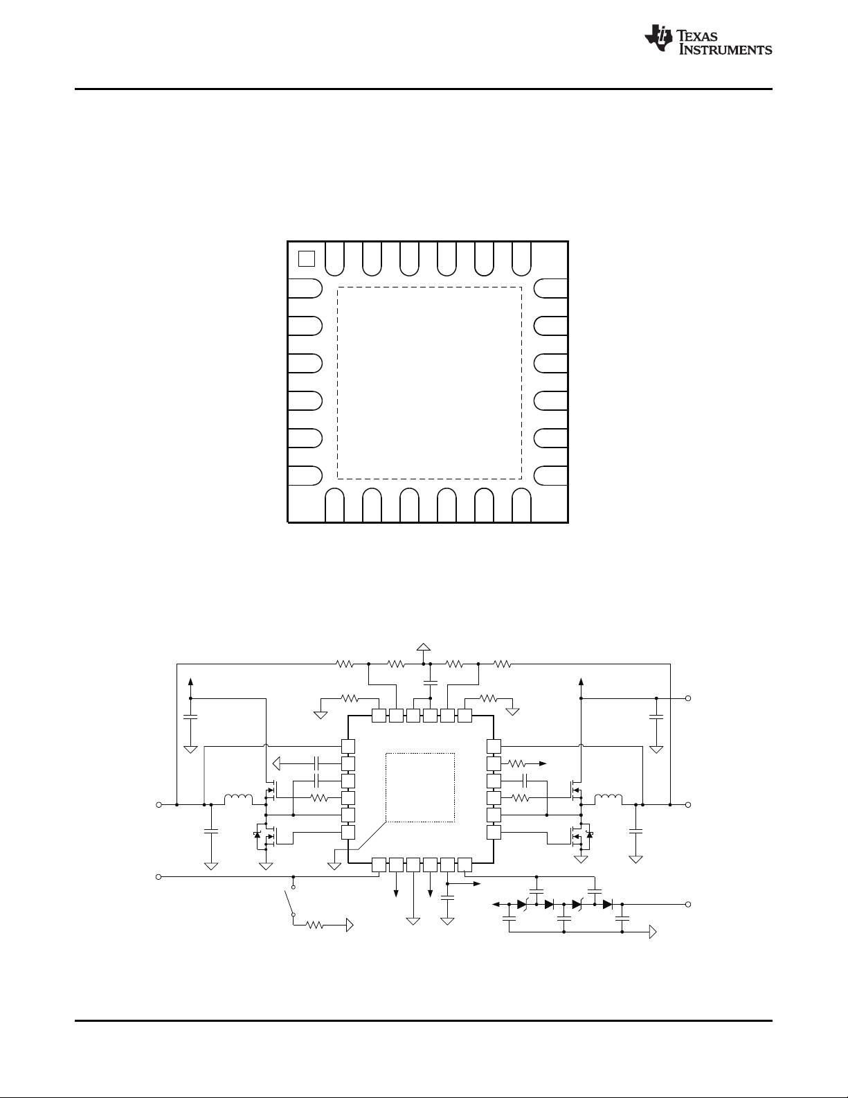
7
8
9
10
24
23
22
21
VO1
PGOOD
VBST1
DRVH1
VO2
VREG3
VBST2
DRVH2
TPS51125ARGE
11
12
20
19
LL1
DRVL1
LL2
DRVL2
13 14 15 16 17 18
EN0
SKIPSEL
GND
VIN
VREG5
VCLK
6 5 4 3 2 1
ENTRIP2
VFB2
TONSEL
VREF
VFB1
ENTRIP1
PowerPAD
220 nF
20 kW 20 kW 30 kW
100 kW
VREG5
10 mF
5.1 W
0.1 mF
130 kW130 kW
3.3 mF
330 mF
VO1
5 V
VIN
VREG5
VIN
10 mF x 2
VIN
5.5 V
to
28 V
EN0
5.1 W
0.1 mF
3.3 mF
330 mF
VO2
3.3 V
10 mF x 2
10 mF
13 kW
VIN
100 nF 1 mF
15 V
100 nF
100 nF
100 nF
620 kW
VO1VREF
TPS51125ARGE
VO1
PGOOD
VO2
VREG3
VBST1
DRVL1
LL1
DRVH1
VBST2
DRVH2
LL2
DRVL2
EN0
ENTRIP2
VFB2
VREF
TONSEL
VFB1
ENTRIP1
SKIPSEL
GND
VIN
VCLK
VREG5
2
3
4
5
6
7 8
9 10
11
1
12
13
14
15
16
17
18
24 23
22 21
20 19
TPS51125A
SLUS976F –SEPTEMBER 2009–REVISED SEPTEMBER 2012
www.ti.com
QFN PACKAGE
24 PINS
(TOP VIEW)
Typical Application Diagram
8 Submit Documentation Feedback Copyright © 2009–2012, Texas Instruments Incorporated
Product Folder Links: TPS51125A
TPS51125A
www.ti.com
SLUS976F –SEPTEMBER 2009–REVISED SEPTEMBER 2012
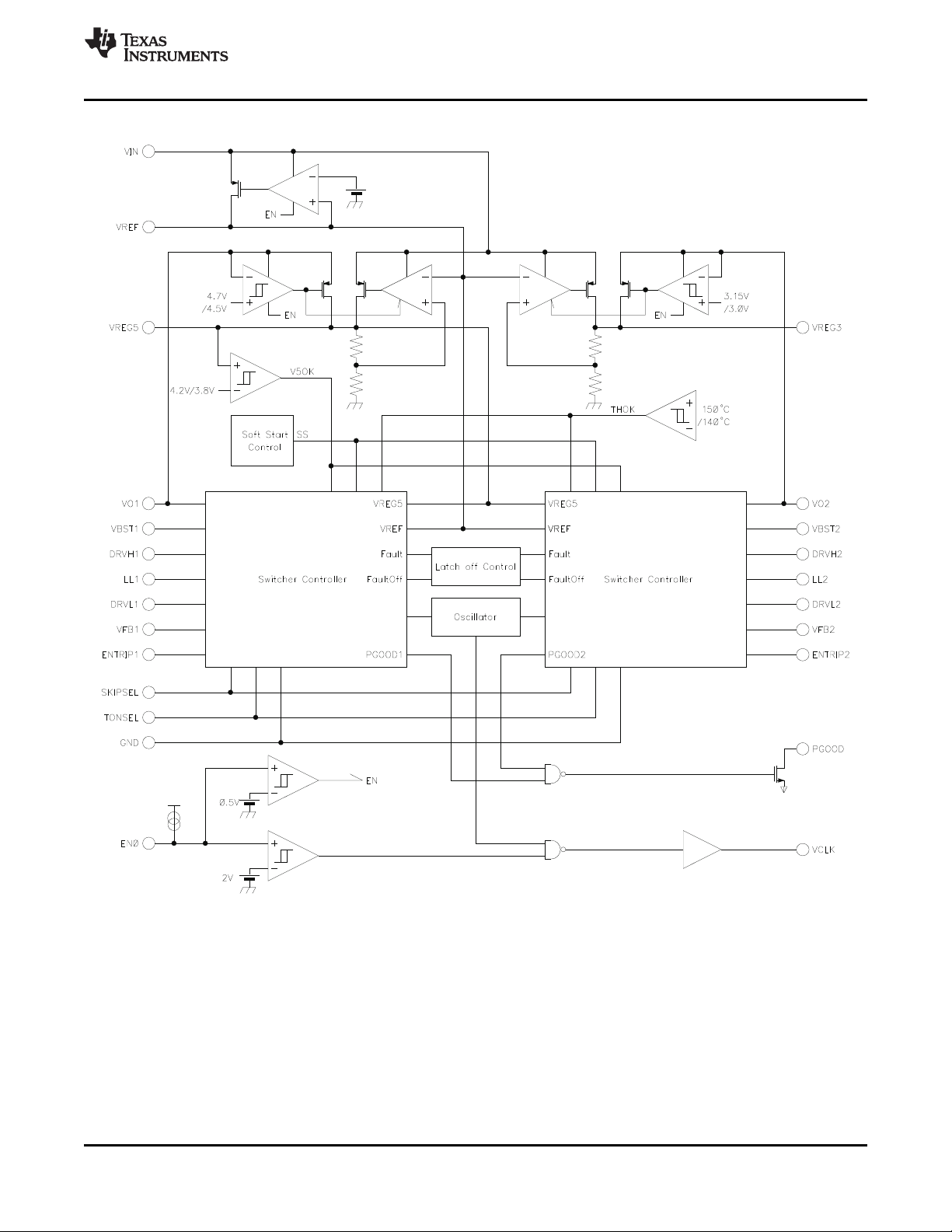
Functional Block Diagram
Copyright © 2009–2012, Texas Instruments Incorporated Submit Documentation Feedback 9
Product Folder Links: TPS51125A
TPS51125A
SLUS976F –SEPTEMBER 2009–REVISED SEPTEMBER 2012
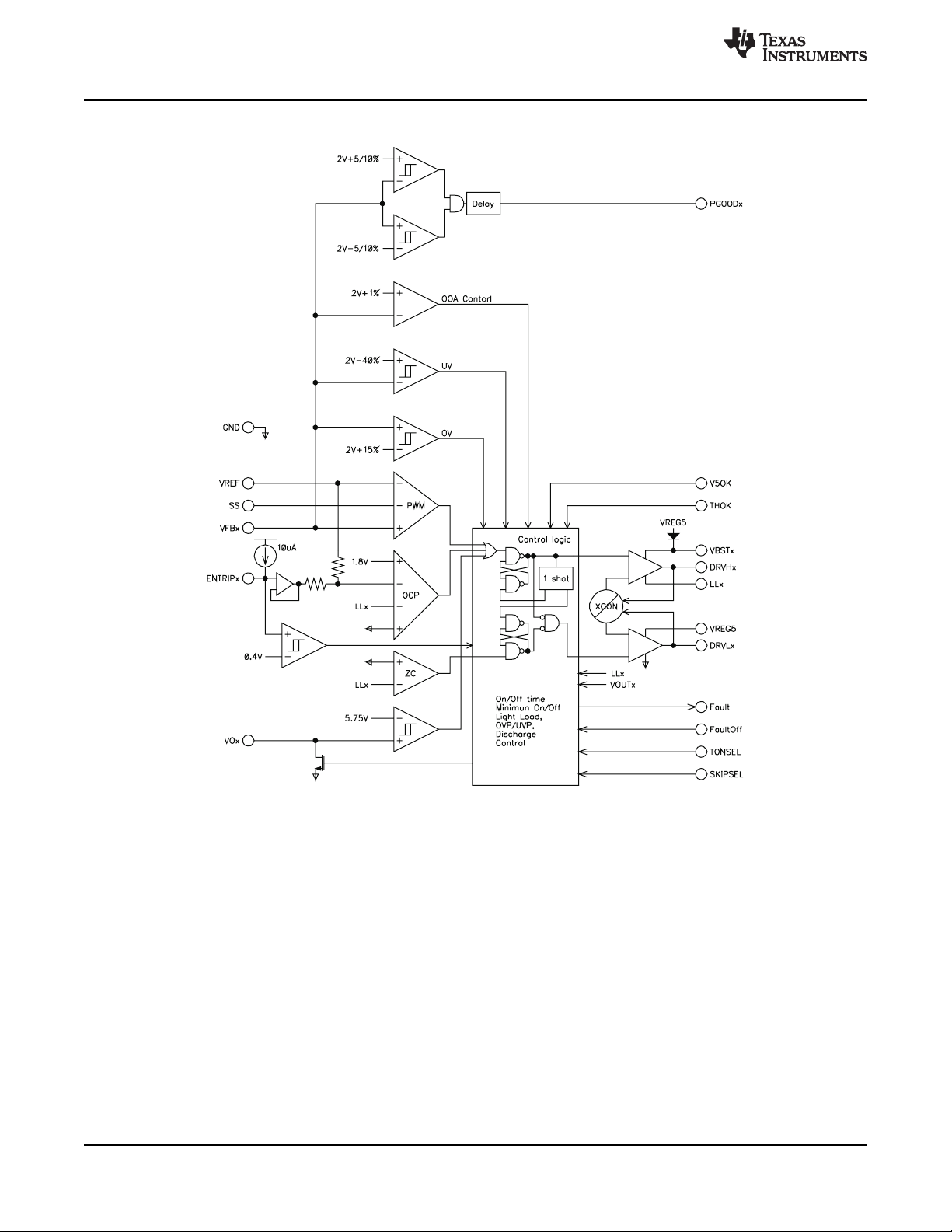
Switcher Controller Block
www.ti.com
10 Submit Documentation Feedback Copyright © 2009–2012, Texas Instruments Incorporated
Product Folder Links: TPS51125A
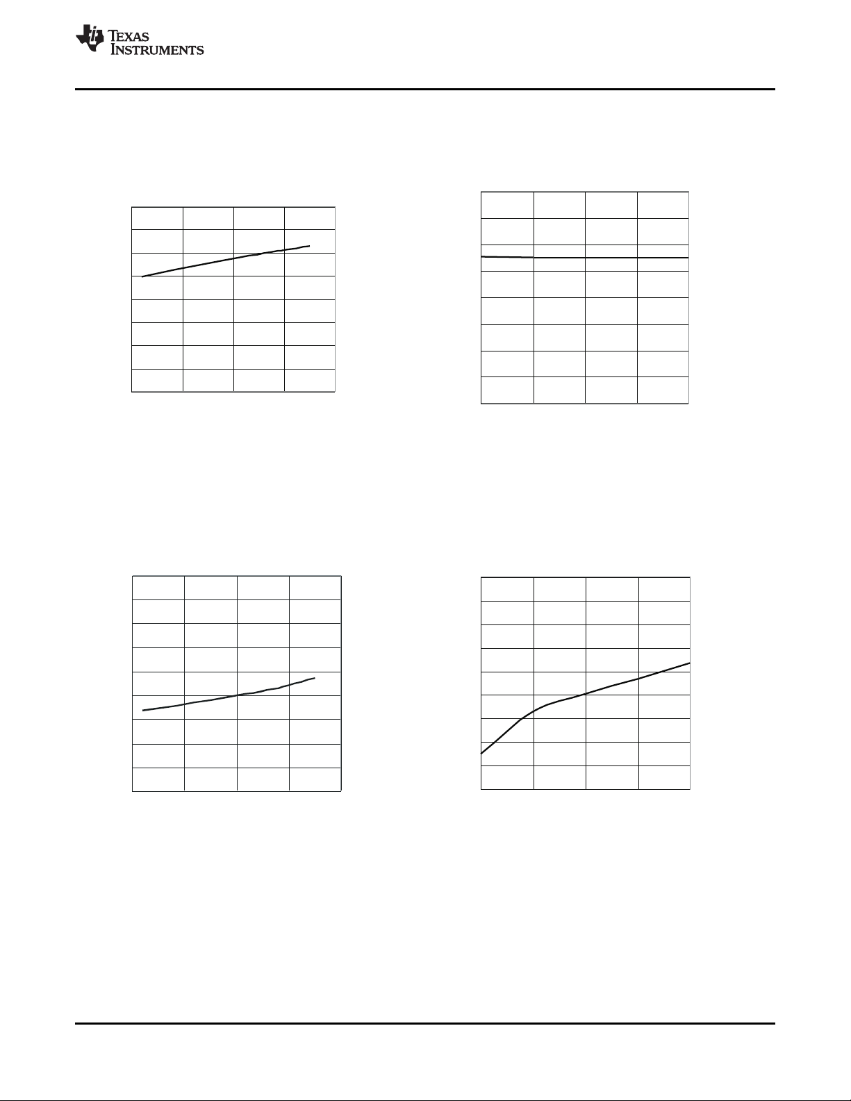
VIN SUPPLY CURRENT2
vs
JUNCTION TEMPERATURE
0
1
2
3
4
5
6
7
8
9
-50 0 50 100 150
TJ- Junction Temperature - °C
I
VIN2
- VIN Supply Current2 - mA
VIN SUPPLY CURRENT2
vs
INPUT VOLTAGE
0
1
2
3
4
5
6
7
8
9
5 10 15 20 25
VIN- Input Voltage - V
I
VIN2
- VIN Supply Current2 - mA
VIN SUPPLY CURRENT1
vs
INPUT VOLTAGE
0
100
200
300
400
500
600
700
800
5 10 15 20 25
VIN- Input Voltage - V
I
VIN1
- VIN Supply Current1 - mA
VIN SUPPLY CURRENT1
vs
JUNCTION TEMPERATURE
0
100
200
300
400
500
600
700
800
-50 0 50 100 150
TJ- Junction Temperature - °C
I
VIN1
- VIN Supply Current1 - m A
TPS51125A
www.ti.com
SLUS976F –SEPTEMBER 2009–REVISED SEPTEMBER 2012
TYPICAL CHARACTERISTICS
Copyright © 2009–2012, Texas Instruments Incorporated Submit Documentation Feedback 11
Figure 1. Figure 2.
Figure 3. Figure 4.
Product Folder Links: TPS51125A
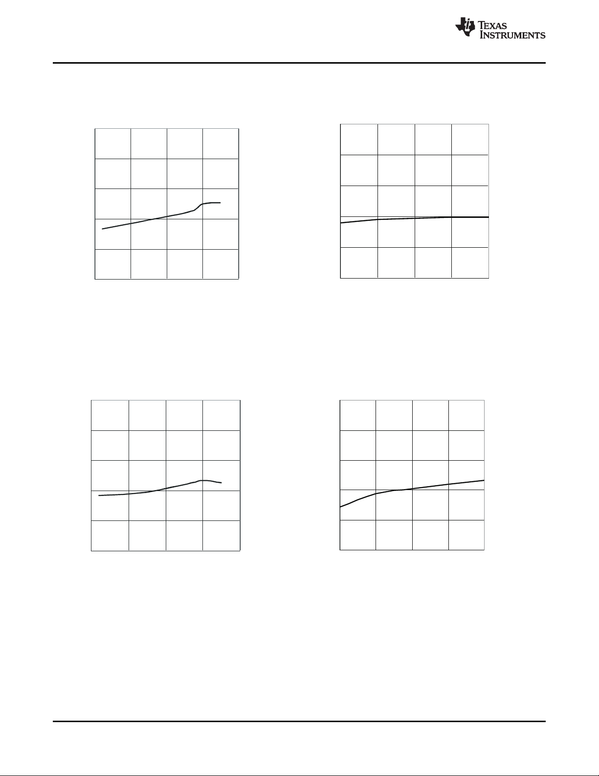
VIN SHUTDOWN CURRENT
vs
INPUT VOLTAGE
0
5
10
15
20
25
5 10 15 20 25
VIN- Input Voltage - V
I
VINSDN
- VIN Shutdown Current - mA
VIN SHUTDOWN CURRENT
vs
JUNCTION TEMPERATURE
0
5
10
15
20
25
-50 0 50 100 150
TJ- Junction Temperature - °C
I
VINS DN
- VIN Shutdown Current - mA
VIN STANDBY CURRENT
vs
JUNCTION TEMPERATURE
0
50
100
150
200
250
-
50
0 50 100 150
TJ- Junction Temperature - °C
I
VINST BY
- VIN Standby Cu rrent - mA
VINSTANDBY CURRENT
vs
INPUTVOLTAGE
0
50
100
150
200
250
5 10 15 20 25
VIN-InputVoltage-V
I – VINStandbyCurrent – A
VINSTBY
m
TPS51125A
SLUS976F –SEPTEMBER 2009–REVISED SEPTEMBER 2012
TYPICAL CHARACTERISTICS (continued)
Figure 5. Figure 6.
www.ti.com
12 Submit Documentation Feedback Copyright © 2009–2012, Texas Instruments Incorporated
Figure 7. Figure 8.
Product Folder Links: TPS51125A
 Loading...