

Texas Instruments tps51124 Datasheet
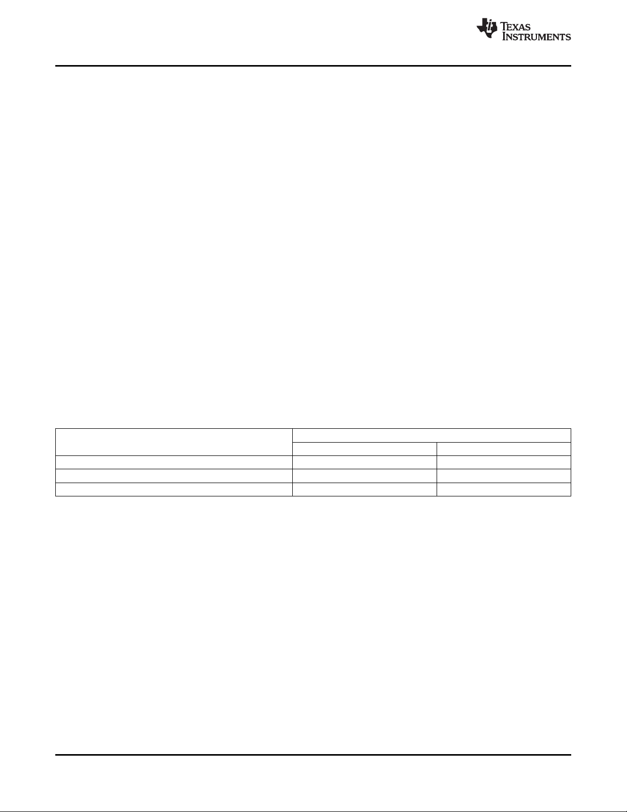
75kΩ
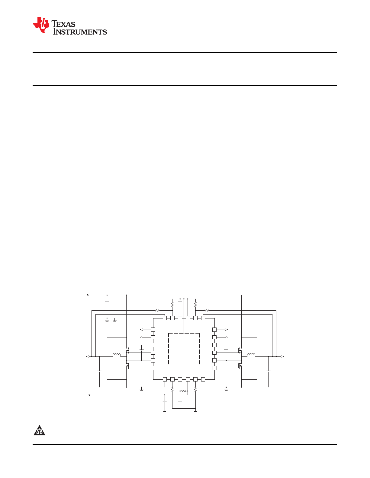
9
10
11
12
PGOOD1
EN1
PGOOD2
EN2
TPS51124RGE
(QFN24)
13 14 15 16
VBST1
DRVL1
LL1
DRVH1
VBST2
DRVH2
LL2
DRVL2
17
8
7
6 5 4 3 2 1
18
19
20
21
22
23
24
VO1
1.05V/10 A
Q2
IRF8113
L1
Q1
IRF7821
VO2
1.5V/10 A
Q4
IRF8113
L2
Q3
IRF7821
InputVoltage
3Vto28V
PowerPAD
TM
C7
R6
C3
C1
C6
C4
R3
6.8
C8
R7
R1
R2
75
R5
R4
V5IN
4.5Vto5.5V
VO2
VO1
VFB2
TONSEL
GND
VFB1
PGND2
TRIP2
V5FILT
V5IN
TRIP1
PGND1
Power
Good2
EN2
C5
C2
Power
Good1
EN1
SGND
PGNDPGND
SGND
C9
SGND PGND
PGND
73.2kΩ
kΩ
28.7kΩ
22µF
2x330µF
1µH
10µF
0.1µF
4.7 μF
6.8kΩ
1 μF
3.3Ω
kΩ
0.1µF
10µF
1µH
2x330µF
TPS51124
www.ti.com
DUAL SYNCHRONOUS STEP-DOWN CONTROLLER FOR
LOW VOLTAGE POWER RAILS
Check for Samples: TPS51124
1
FEATURES
2
• High Efficiency, Low-Power Consumption,
Shutdowns to <1 mA
• Fixed Frequency Emulated On-Time Control,
Frequency Selectable From Three Options
• D-CAP™ Mode Enables Fast Transient
Response
• Auto-Skip Mode
• Less Than 1% Initial Reference Accuracy
• Low Output Ripple
• Wide Input Voltage Range: 3 V to 28 V
• Output Voltage Range: 0.76 V to 5.5 V
• Low-Side R
• Adaptive Gate Drivers With Integrated Boost
Diode
• Internal 1.2-ms Voltage-Servo Soft Start
• Power-Good Signals for Each Channel With
Delay Timer
• Output Discharge During Disable, Fault
APPLICATIONS
• Notebook I/O and Low Voltage System Bus
Loss-less Current Sensing
DS(ON)
SLVS616B –NOVEMBER 2005–REVISED SEPTEMBER 2010
DESCRIPTION
The TPS51124 is a dual, adaptive on-time D-CAP™
mode synchronous buck controller. The part enables
system designers to cost effectively complete the
suite of notebook power bus regulators with the
absolute lowest external component count and lowest
standby consumption. The fixed frequency emulated
adaptive on-time control supports seamless operation
between PWM mode at heavy load condition and
reduced frequency operation at light load for high
efficiency down to milliampere range. The main
control loop for the TPS51124 uses the D-CAP mode
that optimized for low ESR output capacitors such as
POSCAP or SP-CAP promises fast transient
response with no external compensation. Simple and
separate power good signals for each channel allow
flexibility of power sequencing. The part provides a
convenient and efficient operation with supply input
voltages (V5IN, V5FILT) ranging from 4.5 V to 5.5 V,
conversion voltages (drain voltage for the
synchronous high-side MOSFET) from 3 V to 28 V
and output voltages from 0.76 V to 5.5 V.
The TPS51124 is available in 24-pin QFN package
specified from –40°C to 85°C ambient temperature
range.
1
2D-CAP, PowerPAD are trademarks of Texas Instruments.
PRODUCTION DATA information is current as of publication date.
Products conform to specifications per the terms of the Texas
Instruments standard warranty. Production processing does not
necessarily include testing of all parameters.
Please be aware that an important notice concerning availability, standard warranty, and use in critical applications of Texas
Instruments semiconductor products and disclaimers thereto appears at the end of this data sheet.
Copyright © 2005–2010, Texas Instruments Incorporated
TPS51124
SLVS616B –NOVEMBER 2005–REVISED SEPTEMBER 2010
These devices have limited built-in ESD protection. The leads should be shorted together or the device placed in conductive foam
during storage or handling to prevent electrostatic damage to the MOS gates.
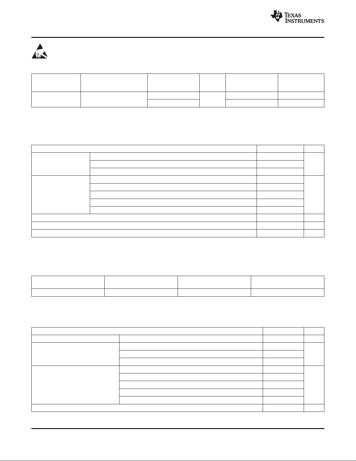
ORDERING INFORMATION
T
A
–40°C to 85°C 24
(1) All packaging options have Cu NIPDAU lead/ball finish.
ABSOLUTE MAXIMUM RATINGS
PACKAGE PART PINS ORDER
Plastic Quad TPS51124RGET Tape-and-Reel 250
Flat Pack (QFN)
(1)
ORDERING MINIMUM
NUMBER QUANTITY
TPS51124RGER Tape-and-Reel 3000
(1)
OUTPUT
SUPPLY
www.ti.com
over operating free-air temperature range (unless otherwise noted)
VALUE UNIT
Input voltage
range
Output voltage
range
T
T
T
(1) Stresses beyond those listed under absolute maximum ratings may cause permanent damage to the device. These are stress ratings
Operating ambient temperature range –40 to 85 °C
A
Storage temperature range –55 to 150 °C
stg
Junction temperature range –40 to 125 °C
J
only and functional operation of the device at these or any other conditions beyond those indicated under recommended operating
conditions is not implied. Exposure to absolute-maximum-rated conditions for extended periods may affect device reliability. All voltage
values are with respect to the network ground terminal unless otherwise noted
VBST1, VBST2 –0.3 to 36
VBST1, VBST2 (wrt LLx) –0.3 to 6 V
V5IN, V5FILT, EN1, EN2, VFB1, VFB2, TRIP1, TRIP2, VO1, VO2, TONSEL –0.3 to 6
DRVH1, DRVH2 –1 to 36
DRVH1, DRVH2 (wrt LLx) –0.3 to 6
LL1, LL2 –2 to 30 V
PGOOD1, PGOOD2, DRVL1, DRVL2 –0.3 to 6
PGND1, PGND2 –0.3 to 0.3
DISSIPATION RATINGS
PACKAGE TA<25°C DERATING FACTOR TA= 85°C
24-pin QFN
(1) Enhanced thermal conductance by 2 × 2 thermal vias beneath thermal pad.
(1)
POWER RATING ABOVE TA= 25°C POWER RATING
2.33 W 23.3 mW/°C 0.93 W
RECOMMENDED OPERATING CONDITIONS
over operating free-air temperature range (unless otherwise noted)
MIN MAX UNIT
Supply input voltage range V5IN, V5FILT 4.5 5.5 V
VBST1, VBST2 –0.1 34
Input voltage range VBST1, VBST2 (wrt LLx) –0.1 5.5 V
EN1, EN2, VFB1, VFB2, TRIP1, TRIP2, VO1, VO2, TONSEL –0.1 5.5
DRVH1, DRVH2 –0.8 34
DRVH1, DRVH2 (wrt LLx) –0.1 5.5
Output voltage range LL1, LL2 –1.8 28 V
PGOOD1, PGOOD2, DRVL1, DRVL2 –0.1 5.5
PGND1, PGND2 –0.1 0.1
T
Operating ambient temperature range –40 85 °C
A
2 Submit Documentation Feedback Copyright © 2005–2010, Texas Instruments Incorporated
Product Folder Link(s): TPS51124
TPS51124
www.ti.com
SLVS616B –NOVEMBER 2005–REVISED SEPTEMBER 2010
ELECTRICAL CHARACTERISTICS
over operating free-air temperature range, V5IN = V5FILT = 5 V (unless otherwise noted)
PARAMETER TEST CONDITIONS MIN TYP MAX UNIT
SUPPLY CURRENT
I
V5FILT
I
V5INSDN
I
V5FILTSD
N
V5FILT supply current EN1 = EN2 = 5 V, VFB1 = VFB2 = 0.77 V, 350 700 mA
V5IN shutdown current V5IN current, no load, EN1 = EN2 = 0 V 1 mA
V5FILT shutdown current V5FILT current, no load, EN1 = EN2 = 0 V 1 mA
VFB VOLTAGE and DISCHARGE RESISTANCE
V
VFB
V
VFB
V
VFBSKIP
I
VFB
R
Dischg
VFB regulation voltage FB voltage, skip mode (f
VFB regulation voltage
tolerance
VFB regulation shift in 0.758-V target for resistor divider. See PWM Operation of
continuous conduction Detailed Description
VFB input current VFBx = 0.758 V, absolute value 0.02 0.1 mA
VO discharge resistance ENx = 0 V, VOx = 0.5 V, TA= 25°C 10 20 Ω
OUTPUT: N-CHANEEL MOSFET GATE DRIVERS
R
R
T
DRVH
DRVL
D
DRVH resistance
DRVL resistance
Dead time
INTERNAL BST DIODE
V
FBST
I
VBSTLK
Forward voltage V
VBST leakage current 0.1 1 mA
ON-TIME TIMER CONTROL AND INTERNAL SOFT START,
T
ON11
T
ON12
T
ON13
T
ON21
T
ON22
T
ON23
T
ON(MIN)
T
OFF(MIN)
T
ss
CH1, 240-kHz setting VO1 = 1.5 V,TONSEL = GND, LL1 = 12 V 440 500 560 ns
CH1, 300-kHz setting VO1 = 1.5 V, TONSEL = FLOAT, LL1 = 12 V 340 390 440 ns
CH1, 360-kHz setting VO1 = 1.5 V,TONSEL = V5FILT, LL1 = 12 V 265 305 345 ns
CH2, 300-kHz setting VO2 = 1.05 V, TONSEL = GND, LL2 = 12 V 235 270 305 ns
CH2, 360-kHz setting VO2 = 1.05 V, TONSEL = FLOAT, LL2 = 12 V 180 210 240 ns
CH2, 420-kHz setting VO2 = 1.05 V, TONSEL = V5FILT, LL2 = 12 V 120 150 180 ns
CH2 On time VO2 = 0.76 V, TONSEL = V5FILT, LL2 = 28 V 80 110 140 ns
CH1/CH2 Min. off time LL = –0.1 V, TA= 25°C, VFB = 0.7 V 435 ns
Internal SS time 0.85 1.2 1.40 ms
(1) Specified by design. Not production tested.
V5FILT current, no load,
LL1=LL2=0.5V
/10) 764 mV
PWM
TA= 25°C, bandgap initial accuracy –0.9% 0.9%
TA= 0°C to 85°C
TA= –40°C to 85°C
Source, V
Sink, V
DRVHx-LLx
Source, V
Sink, V
DRVLx–PGNDx
(1)
(1)
(1)
VBSTx–DRVHx
= 0.5 V 5 7 Ω
= 0.5 V 1.5 2.5 Ω
V5IN–DRVLx
= 0.5 V 4 6 Ω
= 0.5 V 1 2.0 Ω
DRVHx-low (DRVHx = 1 V) to DRVLx-on
(DRVLx = 4 V), LL = –0.05 V,
DRVLx-low (DRVLx = 1 V) to DRVHx-on
(DRVHx = 4 V), LL = –0.05 V,
V5IN–VBSTx
, IF= 10 mA, TA= 25°C 0.7 0.8 0.9 V
VBST = 34 V, LL = 28 V, VOx = 5.5 V,
TA= 25°C
Internal soft start, time from ENx > 3 V to VFBx regulation value
= 735 mV
–1.3% 1.3%
–1.6% 1.6%
758 mV
10 20 50 ns
30 40 60 ns
Copyright © 2005–2010, Texas Instruments Incorporated Submit Documentation Feedback 3
Product Folder Link(s): TPS51124
TPS51124
SLVS616B –NOVEMBER 2005–REVISED SEPTEMBER 2010
ELECTRICAL CHARACTERISTICS (Continued)
over operating free-air temperature range, V5IN = V5FILT = 5 V (unless otherwise noted)
PARAMETER TEST CONDITIONS MIN TYP MAX UNIT
UVLO/LOGIC THRESHOLD
V
UV5VFILT
V
EN
I
EN
V
TONSEL
I
TONSEL
V5FILT UVLO threshold
ENx threshold
ENx input current Absolute value
TONSEL threshold Medium
TONSEL input current
CURRENT SENSE
I
TRIP
TC
V
OCLoff
V
ZC
V
Rtrip
ITRIP
TRIP source current VTRIPx < 0.3 V, TA= 25°C 9 10 11 mA
I
temperature coeffficent On the basis of 25°C
TRIP
OCP compensation offset –10 0 10 mV
Zero cross detection comparator VPGNDx-LLx voltage, PGOODx = Hi
offset
Current limit threshold setting V
range
POWER-GOOD COMPARATOR
V
THPG
I
PGMAX
T
PGDEL
PG threshold
PG sink current PGOODx = 0.5 V 2.5 5.0 mA
PG delay Delay for PG in 400 510 620 ms
OUTPUT UNDERVOLTAGE AND OVERVOLTAGE PROTECTION
V
OVP
t
OVPDEL
V
UVP
t
UVPDEL
t
UVPEN
Output OVP trip threshold OVP detect 110% 115% 120%
Output OVP prop delay 1.5 ms
Output UVP trip threshold
Output UVP delay 20 32 40 ms
Output UVP enable delay After 1.7 × Tss, UVP protection engaged 1.4 2 2.4 ms
THERMAL SHUTDOWN
T
SDN
Thermal shutdown threshold °C
(1) Ensured by design. Not production tested.
Wake up 3.7 4.0 4.3 V
Hysteresis 0.2 0.3 0.4 V
Wake up 1.0 1.3 1.5 V
Hysteresis 0.2 V
(1)
(1)
Fast
(1)
(1)
Slow
TONSEL=0V, current out of the pin
TONSEL=5V, current in to the pin
(1)
(V
TRIPx-GND
V
TRIPx-GND
TRIPx-GND
– V
PGNDx-LLx
= 60 mV
) voltage,
voltage, all temperatures
(1)
(1)
(1)
(1)
PG in from lower (PGOODx goes hi) 92.5% 95% 97.5%
PG low hysteresis (PGOODx goes low) –5%
PG in from higher (PGOODx goes hi) 102.5% 105% 107.5%
PG high hysteresis (PGOODx goes low) 5%
UVP detect 65% 70% 75%
Hysteresis (recovery < 20 ms) 10%
Shutdown temperature
Hysteresis
(1)
(1)
0.02 0.1 mA
V5FILT
–0.3
2 V
V5FILT
1 mA
1 mA
4200 ppm/°C
0.5 mV
30 200 mV
160
10
www.ti.com
V
–1.0
0.5 V
4 Submit Documentation Feedback Copyright © 2005–2010, Texas Instruments Incorporated
Product Folder Link(s): TPS51124
PGOOD1
EN1
VBST1
DRVH1
LL1
DRVL1
24 23 22 21 20 19
PGND1
TRIP1
V5IN
V5FILT
TRIP2
PGND2
VO1
VFB1
GND
TONSEL
VFB2
VO2
18
17
16
15
14
13
1
2
3
4
5
6
PGOOD2
EN2
VBST2
DRVH2
LL2
DRVL2
7 8 9 10 11 12
TPS51124
www.ti.com
SLVS616B –NOVEMBER 2005–REVISED SEPTEMBER 2010
DEVICE INFORMATION
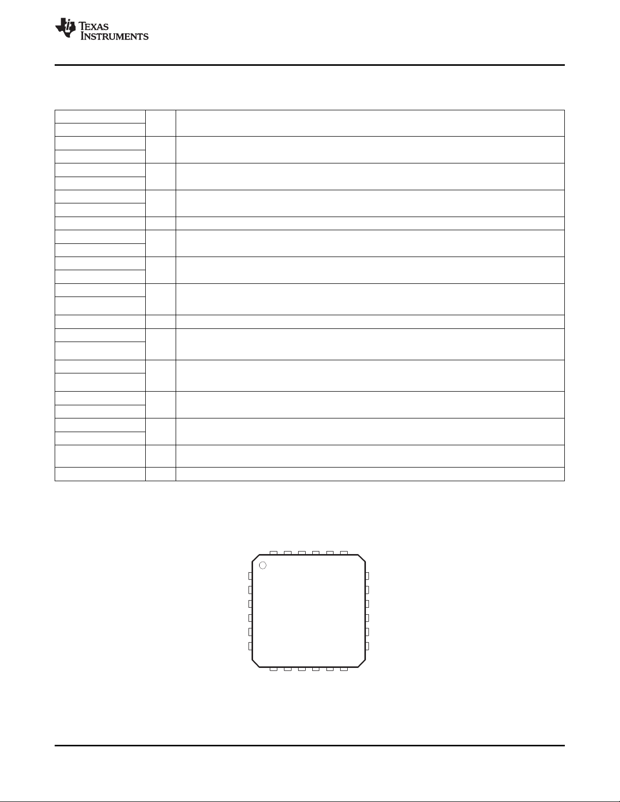
PIN FUNCTIONS
PIN
NAME NO.
DRVH1 21
DRVH2 10
DRVL1 19
DRVL2 12
EN1 23
EN2 8
GND 3 I Signal ground pin
LL1 20
LL2 11
PGND1 18
PGND2 13
PGOOD1 24 Power Good window comparator open drain output for channel 1 and 2. Pull up with a resistor to 5 V, or
PGOOD2 7
TONSEL 4 I On-time selection pin. See Table 1.
TRIP1 17 Over-current trip point set input. Connect resistor from this pin to GND to set threshold for synchronous
TRIP2 14
VBST1 22 Supply input for synchronous high-side MOSFET driver (Boost Terminal). Connect capacitor from this pin
VBST2 9
VFB1 2
VFB2 5
VO1 1
VO2 6
V5FILT 15 I
V5IN 16 I 5-V power supply input for FET gate drivers. Internally connected to VBSTx by PN diodes.
I/O DESCRIPTION
Synchronous high-side MOSFET driver outputs. LL node referenced floating drivers. The gate drive
O
voltage is defined by the voltage across VBST to LL node flying capacitor.
Synchronous low-side MOSFET driver outputs. PGND referenced drivers. The gate drive voltage is
O
defined by V5IN voltage.
I Channel 1 and channel 2 enable pins. Connect to 5 V or 3.3 V to turn on SMPS
Switch node connections for high-side drivers return. Also serve as input to current comparators and input
I/O
voltage monitor for on-time control circuitry.
Ground returns for DRVL1 and DRVL2. Also serve as input of current comparators. Connect PGND1,
I/O
PGND2, and GND strongly together near the IC. Output discharge current flows through this pin, also.
O appropriate signal voltage. Current capability is 5 mA. PGOOD goes high 0.5 ms after VFB comes within
specified limits. Power bad, or the terminal goes low, is within 10 ms.
I low-side R
over-current comparator.
sense. Voltage across this pin and GND is compared to voltage across PGND and LL at
DS(on)
I to respective LL terminals. An internal PN diode is connected between V5IN to each of these pins. User
can add external Schottky diode if forward drop is critical to drive the MOSFET.
I SMPS voltage feedback inputs. Connect with feedback resistor divider.
Output connections to SMPS. These terminals serve two functions: On-time adjustment and output
I
discharge.
5-V power supply input for the entire control circuit except the MOSFET drivers. Connect RC low-pass
filter from V5IN to V5FILT.
QFN PACKAGE
(TOP VIEW)
Copyright © 2005–2010, Texas Instruments Incorporated Submit Documentation Feedback 5
Product Folder Link(s): TPS51124
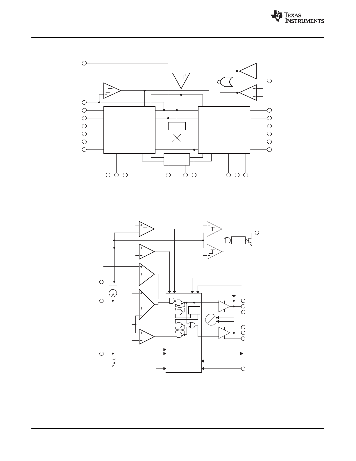
Ref −30/10%
UV
OV
Ref +15%
Ref
758 mV
SSx
VFBx
TRIPx
10 µA
GND
LLx
PGNDx
LLx
VOx
LLx
PGNDx
LLx
ONx
ZC
OCP
PWM
Ref +5/10%
Ref −5/10%
Control Logic
1
Shot
On/Off T ime
Minimum On/Off
Light Load,
OVP/UVP,
Discharge
Control
PGNDx
Delay
XCON
T ONSEL
Sdn
Fault
DRVLx
V5IN
V5IN
LLx
DRVHx
VBSTx
THOK
V5OK
PGNDx
PGOODx
V5IN
4 V/3.7 V
V5OK
THOK
BGR
V5FIL T
VO1
VBST1
DRVH1
LL1
DRVL1
PGND1
Switcher Controller
V5DRV
Ref
Fault
Sdn
ON1
SS1
ANALOG/SUB GND
EN/SS
Control
TRIP1
VFB1
PGOOD1
EN1
EN2
GND
PGOOD2
VFB2
TRIP2
SS2
ON2
Sdn
Fault
Ref
V5DRV
Switcher Controller
VO2
VBST2
DRVH2
LL2LL2
DRVL2
PGND2
1 V
T ONSEL
4 V
Frequency Control
FAST
SLOW
160 °C/
150 °C
MID
TPS51124
SLVS616B –NOVEMBER 2005–REVISED SEPTEMBER 2010
FUNCTIONAL BLOCK DIAGRAM
www.ti.com
6 Submit Documentation Feedback Copyright © 2005–2010, Texas Instruments Incorporated
Product Folder Link(s): TPS51124

I
OUT(LL)
+
1
2 L ƒ
ǒ
VIn* V
OUT
Ǔ
V
OUT
V
IN
TPS51124
www.ti.com
SLVS616B –NOVEMBER 2005–REVISED SEPTEMBER 2010
DETAILED DESCRIPTION
PWM OPERATION
The main control loop of the switching mode power supply (SMPS) is designed as an adaptive on-time pulse
width modulation (PWM) controller. It supports a proprietary D-CAP Mode. D-CAP Mode uses an internal
compensation circuit and is suitable for low external component-count configuration, with appropriate amount of
ESR at the output capacitor(s). The output voltage is monitored at a feedback point voltage. The reference
voltage at the feedback point is a combination of a fixed 0.750-V precision reference and a synchronized,
precision 15-mV ramp signal. Lower output voltages in notebook systems (e.g., 1.05 V, 1.5 V) require extremely
low output ripple. By providing a ramp signal, the TPS51124 is easier to use in low-output ripple systems. The
combination of the precision ramp and reference yield an effective target reference of 0.758 V. The accuracy of
this effective reference remains 1.3% over line and temperature.
At the beginning of each cycle, the synchronous high-side MOSFET is turned on, or becomes ON state. This
MOSFET is turned off, or becomes OFF state, after the internal one-shot timer expires. This one shot is
determined by the converter’s input voltage, VIN, and the output voltage, VOUT, to keep the frequency fairly
constant over the input voltage range; hence, it is called adaptive on-time control (see PWM Frequency and
Adaptive On-time Control). The high-side MOSFET is turned on again when feedback information indicates
insufficient output voltage, and inductor current information indicates a below-the-over-current limit condition.
Repeating operation in this manner, the controller regulates the output voltage. The synchronous low-side
MOSFET is turned on each OFF state to keep the conduction loss at a minimum. The low-side MOSFET is
turned off when the inductor current information detects zero level. This enables seamless transition to the
reduced frequency operation at light-load conditions so that high efficiency is kept over a broad range of load
current.
LIGHT-LOAD CONDITION
TPS51124 automatically reduces switching frequency at light-load conditions to maintain high efficiency. This
reduction of frequency is achieved smoothly and without increase of Vout ripple or load regulation. Detail
operation is described as follows. As the output current decreases from heavy-load condition, the inductor
current is also reduced, and eventually comes to the point that its valley touches zero current, which is the
boundary between continuous conduction and discontinuous conduction modes. The low-side MOSFET is turned
off when this zero inductor current is detected. As the load current is further decreased, the converter runs in
discontinuous conduction mode and it takes longer and longer to discharge the output capacitor to the level that
requires the next ON cycle. The ON time is kept the same as that in the heavy-load condition. In reverse, when
the output current increases from light load to heavy load, the switching frequency increases to the preset value
as the inductor current reaches the continuous conduction. The transition load point to the light-load operation,
I
OUT(LL)
where f is the PWM switching frequency.
Switching frequency versus output current in the light-load condition is a function of L, f, Vin, and Vout, but it
decreases almost proportional to the output current from the I
It should be noted that in the PWM control path is a small ramp . This ramp is transparent in normal, continuous
conduction mode and does not measurably affect the regulation voltage. However, in discontinuous, light-load
mode, an upward shift in regulation voltage of about 0.75% will be observed. The variation of this shift minimally
affects the reference tolerance. Therefore, the reference value in skip mode is 0.764 V ±1.3% over line and
temperature.
(i.e., the threshold between continuous and discontinuous conduction mode) can be calculated as follows;
(1)
OUT(LL)
given in Equation 1.
Copyright © 2005–2010, Texas Instruments Incorporated Submit Documentation Feedback 7
Product Folder Link(s): TPS51124
TPS51124
SLVS616B –NOVEMBER 2005–REVISED SEPTEMBER 2010
www.ti.com
DETAILED DESCRIPTION (continued)
LOW-SIDE DRIVER
The low-side driver is designed to drive high current low R
represented by its internal resistances, which are 4 Ω for V5IN to DRVLx, and 1 Ω for DRVLx to PGNDx. A dead
time to prevent shoot through is internally generated between high-side MOSFET off to low-side MOSFET on,
and low-side MOSFET off to high-side MOSFET on. A 5-V bias voltage is delivered from V5IN supply. The
instantaneous drive current is supplied by an input capacitor connected between V5IN and GND. The average
drive current is equal to the gate charge at Vgs = 5 V times switching frequency. This gate drive current, as well
as the high-side gate drive current times 5 V, makes the driving power that needs to be dissipated from
TPS51124 package.
N-channel MOSFET(s). The drive capability is
DS(on)
HIGH-SIDE DRIVER
The high-side driver is designed to drive high-current, low R
floating driver, 5-V bias voltage is delivered from V5IN supply. The average drive current is also calculated by the
gate charge at Vgs = 5 V times switching frequency. The instantaneous drive current is supplied by the flying
capacitor between VBSTx and LLx pins. The drive capability is represented by its internal resistances, which are
5 Ω for VBSTx to DRVHx and 1.5 Ω for DRVHx to LLx.
N-channel MOSFET(s). When configured as a
DS(on)
PWM FREQUENCY AND ADAPTIVE ON-TIME CONTROL
TPS51124 employs adaptive on-time control scheme and does not have a dedicated oscillator on board.
However, the part runs with pseudo-constant frequency by feed-forwarding the input and output voltage into the
on-time one-shot timer. The frequencies are set by TONSEL terminal connection as Table 1. The on-time is
controlled inverse proportional to the input voltage and proportional to the output voltage so that the duty ratio is
kept as VOUT/VIN technically with the same cycle time. Although the TPS51124 does not have a pin connected
to VIN, the input voltage is monitored at LLx pin during the ON state. This helps pin count reduction to make the
part compact without sacrificing its performance.
Table 1. TONSEL Connection and Switching Frequency Table
(Frequencies Are Approximate)
TONSEL CONNECTION SWITCHING FREQUENCY
CH1 CH2
GND 240 kHz 300 kHz
FLOAT (Open) 300 kHz 360 kHz
V5FILT 360 kHz 420 kHz
SOFT START
The TPS51124 has an internal, 1.2-ms, voltage servo soft start for each channel. When the ENx pin becomes
high, an internal DAC begins ramping up the reference voltage to the PWM comparator. Smooth control of the
output voltage is maintained during start-up. As TPS51124 shares one DAC with both channels, if ENx pin is set
to high while another channel is starting up, soft start is postponed until another channel soft start has
completed. If both of EN1 and EN2 are set high at a same time, both channels start up at same time.
POWER GOOD
The TPS51124 has power-good output for both switcher channels. The power-good function is activated after
soft start has finished. If the output voltage becomes within ±5% of the target value, internal comparators detect
power good state and the power good signal becomes high after a 510-ms internal delay. During start-up, this
internal delay starts after 1.7 times internal soft-start time to avoid a glitch of power-good signal. If the feedback
voltage goes outside of ±10% of the target value, the power-good signal becomes low after 10-ms internal delay.
Also note that if the feedback voltage goes +10% above target value and the power-good signal flags low, then
the loop attempts to correct the output by turning on the low-side driver (forced PWM mode). After the feedback
voltage returns to be within +5% of the target value and the power-good signal goes high, the controller returns
back to auto-skip mode.
8 Submit Documentation Feedback Copyright © 2005–2010, Texas Instruments Incorporated
Product Folder Link(s): TPS51124
 Loading...