

TPS51120
www.ti.com
SLUS670A–JULY 2005–REVISED AUGUST 2005
DUAL CURRENT MODE, SYNCHRONOUS STEP-DOWN CONTROLLER WITH 100-mA
STANDBY REGULATORS FOR NOTEBOOK SYSTEM POWER
FEATURES DESCRIPTION
• 3.3-V and 5-V 100-mA Bootstrapped Standby
Regulators with Independent Enables
• Selectable D-CAP®Mode Enables Fast
Transient Response Less than 100 ns
• Selectable Low Ripple Current Mode
• Less than 1% Internal Reference Accuracy
• Selectable PWM-only/Auto-skip Modes
• Low-side R
• R
Accurate Current Sense Option
SENSE
• Internal Soft-start and Integrated V
Loss-less Current Sensing
DS(on)
OUT
Discharge Transistors
• Integrated 2-V Reference
• Adaptive Gate Drivers with Integrated Boost
Diode
• Power Good for Each Channel with Delay
Timer
• Fault Disable Mode
• Supply Input Voltage Range: 4.5 V to 28 V
APPLICATIONS
• Notebook Computers System Bus and I/O
The TPS51120 is a highly sophisticated dual current
mode synchronous step-down controller. It is a full
featured controller designed to run directly off a threeor four-cell Li-ion battery and provide high-power and
5-V and/or 3.3-V standby regulation for all the downstream circuitry in a notebook computer system. High
current, 100-mA, 5-V or 3.3-V on-board linear regulators have glitch-free switch over function to SMPS
and can be kept alive independently during standby
state. The pseudo-constant frequency adaptive
on-time control scheme supports full range of current
mode operation including simplified loop compensation, ceramic output capacitors as well as seamless
transition to reduced frequency operation at light-load
condition. Optional D-CAP™ mode operation
optimized for SP-CAP or POSCAP output capacitors
allows further reduction of external compensation
parts. Dynamic UVP supports VIN line sag without
latch off by hitting 5V UVP. No negative voltage
appears at output voltage node during UVLO, UVP,
and OCP, OTP or loss of VIN.
The TPS51120 32-pin QFN package is specified from
–40°Cto85°C ambient temperature.
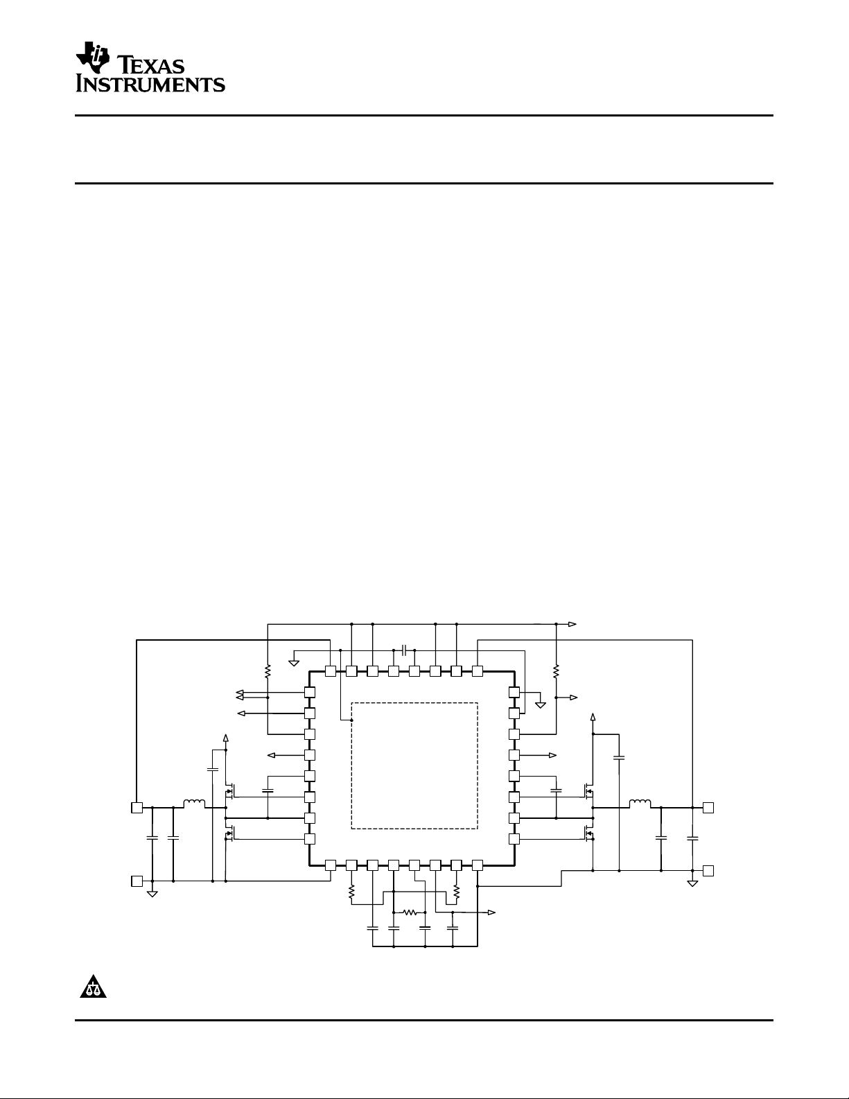
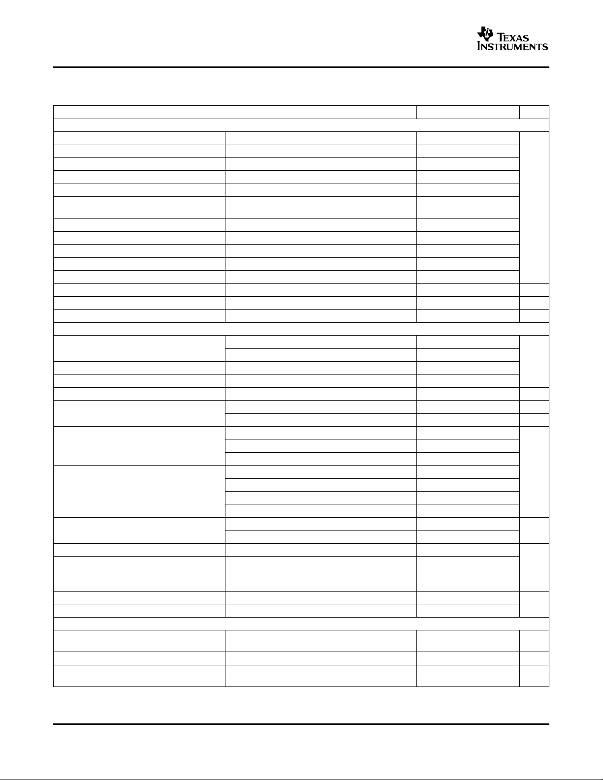
C31
1 nF
V5FILT
R21
VO2
3.3V/6A
+
C2B
150 µF
−VO2_GND
PGND2
20 µF
2.2 µH
C2A
150 µF
C10
L2
EN_LDO5
P_GOOD2
EN_LDO3
VBAT
100 kΩ
Q3
IRF7821
IRF7832
EN_2
Q4
C21
0.1 µF
GND
9
10
11
12
13
14
15
16
8
EN5
EN3
PGOOD2
EN2
VBST2
DRVH2
LL2
DRVL2
PGND2
17
R22
3.3 kΩ
Please be aware that an important notice concerning availability, standard warranty, and use in critical applications of Texas
Instruments semiconductor products and disclaimers thereto appears at the end of this data sheet.
D-CAP is a registered trademark of Texas Instruments.
PRODUCTION DATA information is current as of publication date.
Products conform to specifications per the terms of the Texas
Instruments standard warranty. Production processing does not
necessarily include testing of all parameters.
VO2
7
COMP2
CS2
18
C30
10 µF
6
VREG3
19
VFB2
5
4
GND
VREF2
TPS51120RHB
(QFN−32)
V5FILT
V5REG
20
21
R50
5.1
W
C51
1 µF
3
VFB1
PowerPAD
VIN
22
C50
10 µF
2
COMP1
CS1
23
R12
3.6 kΩ
C30
GND
R11
100 kΩ
EN_1
C11
0.1 µF
P_GOOD1
VBAT
IRF7821
IRF7832
C10
20 µF
Q1
L1
4.7 µH
Q2
C1A
150 µF
PGND1
+
C1B
150 µF
−
VO1
5V/6A
VO1_GND
UDG−05074
1
VO1
32
SKIPSEL
31
TONSEL
30
PGOOD1
29
EN1
28
VBST1
27
DRVH1
26
LL1
DRVL1
25
PGND1
24
VBAT
NA
Copyright © 2005, Texas Instruments Incorporated
www.ti.com
TPS51120
SLUS670A–JULY 2005–REVISED AUGUST 2005
ORDERING INFORMATION
T
A
-40°Cto85°C32
PACKAGE PART PINS ORDER ECO PLAN
PLASTIC QUAD Green
FLAT PACK (QFN) (RoHS and no Sb/Br)
(1) All packaging options have Cu NIPdAu lead/ball finish.
(2) For the most current package and ordering information, see the Package Option Addendum at the end of this document, or see the TI
website at www.ti.com.
ORDERABLE MINIMUM
NUMBER QUANTITY
TPS51120RHBT Tape-and-reel 250
TPS51120RHBR Tape-and-reel 3000
(1)(2)
OUTPUT
SUPPLY
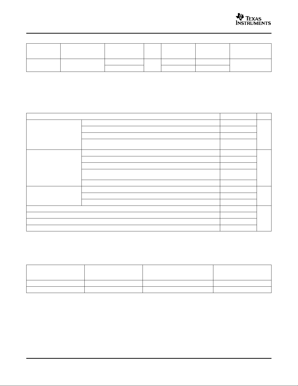
ABSOLUTE MAXIMUM RATINGS
(1)
over operating free-air temperature range unless otherwise noted
TPS51120 UNITS
VBST1, VBST2 -0.3 to 36
VBST1, VBST2 wrt LL -0.3 to 6
Input voltage range V
Output voltage range V
Source/sink current VBST 100 mA
T
Operating ambient temperature range -40 to 85
A
T
Storage temperature -55to150
stg
T
Junction temperature -40to125
J
Lead temperature 1.6 mm (1/16 inch) from case for 10 seconds 255
(1) Stresses beyond those listed under absolute maximum ratings may cause permanent damage to the device. These are stress ratings
only, and functional operation of the device at these or any other conditions beyond those indicated under recommended operating
conditions is not implied. Exposure to absolute-maximum-rated conditions for extended periods may affect device reliability. All voltage
values are with respect to the network ground terminal unless otherwise noted.
VIN, EN5 -0.3 to 30
SKIPSEL, TONSEL, EN1, EN2, CS1, CS2, V5FILT, VFB1, VFB2, EN3, VO1,
VO2
-0.3 to 6
DRVH1, DRVH2 -1 to 36
DRVH1, DRVH2 (wrt LL) -0.3 to 6
LL1, LL2 -1 to 30
VREF2, VREG3, VREG5, PGOOD1, PGOOD2, DRVL1, DRVL2, COMP1,
COMP2
-0.3 to 6
PGND1, PGND2 -0.3 to 0.3
VREF2 1
VREG5, VREG3 (source only) 200
°C
DISSIPATION RATINGS
PACKAGE ABOVE TA=25°C POWER RATING
32-pin QFN
32-pin QFN
(1)
(2)
TA<25°C POWER RATING
(W)
2.6 0.026 1.0
2.9 0.029 1.2
(1) JEDEC standard PCB.
(2) Enhanced thermal conductance by 3 x 3 thermal vias beneath thermal pad.
2
DERATING FACTOR TA=85°C
(W/°C) (W)

TPS51120
www.ti.com
SLUS670A–JULY 2005–REVISED AUGUST 2005
RECOMMENDED OPERATING CONDITIONS
MIN MAX UNIT
Input voltage, V5FILT 4.5 5.5 V
VBST1, VBST2 -0.1 34
VBST1, VBST2 wrt LL -0.1 5.5
Input voltage range VIN, EN5 -0.1 28 V
SKIPSEL, TONSEL, EN1, EN2, CS1, CS2, V5FILT, VFB1, VFB2, EN3 -0.1 5.5
VO1, VO2 -0.1 5.5
DRVH1, DRVH2 -0.8 34
DRVH1, DRVH2 (wrt LL) -0.1 5.5
Output voltage range V
Source/sink current VBST 50 mA
Operating ambient temperature range, T
LL1, LL2 -0.8 28
VREF2, VREG5, VREG3, PGOOD1, PGOOD2, DRVL1, DRVL2, COMP1,
COMP2
PGND1, PGND2 -0.1 0.1
VREF2 0.08
VREG5, VREF3 (source only) 100
A
-0.1 5.5
-40 85 °C
3
www.ti.com
TPS51120
SLUS670A–JULY 2005–REVISED AUGUST 2005
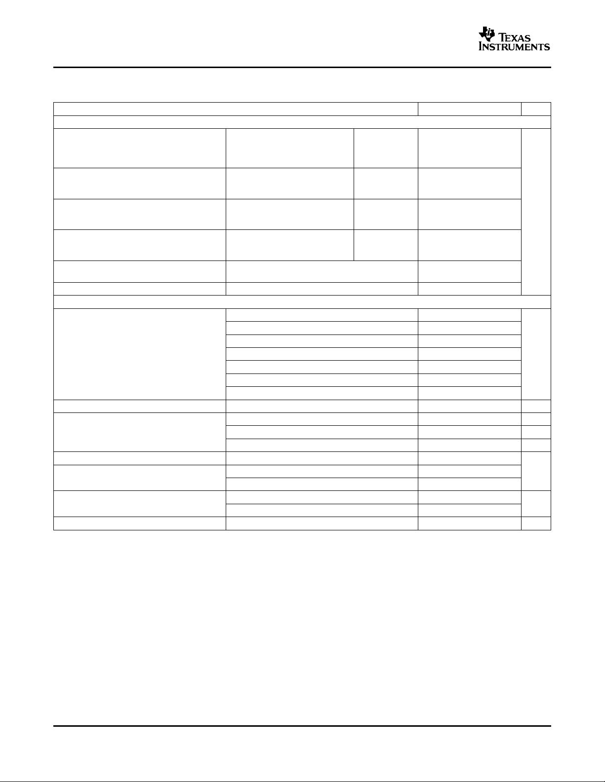
ELECTRICAL CHARACTERISTICS
over operating free-air temperature range, V
PARAMETER TEST CONDITIONS MIN TYP MAX UNIT
SUPPLY CURRENT
I
INCCAP
I
INNOCAP
I
IN5(STBY)
I
IN3(STBY)
I
IN532(STBY)
I
IN(SHDN)
VOUT and VREF2 VOLTAGES
V
OUT
V
ADJ
V
ADJ T
V
VREF2
V
VREF2T
I
VFB
R
DISCHARG
Supply current Current mode 750 1500
Supply current Load, EN3=EN5=FLOAT; D-CAP mode 700 1400
Stand-by current EN3=0V, EN5=FLOAT, 5-V only 30 45
Stand-by current EN3=FLOAT, EN5=0, 3.3-V only 12 20
Stand-by current 100 150
Shut down current VIN current, EN3=EN5=EN1=EN2=0V 10 20
Output voltage V
Output regulation voltage Adjustable mode 1.00 V
Output regulation voltage tolerance
2-V output regulation voltage I
2-V output regulation voltage tolerance
VFB input current µA
Discharge switch resistance VOx=0.5V, TA=25°C1020Ω
=12V,V
VIN
VREG5=VV5FILT
= 5 V (unless otherwise noted)
VIN current, VREG5=VREG3=No
Load, EN3=EN5=FLOAT,
EN1=EN2=5V, CS=5V, COMP
connected to Cap
VIN current, VREG5=VREG3=No
EN1=EN2=5V, CS=5V, COMP=5V
VIN current, VREG5=No Load
EN1=EN2=0
VIN current, VREG3=No Load
EN1=EN2=0
VIN current, VREG5=VREG3=VREF2=No Load
EN3=EN5=FLOAT, EN1=EN2=0
V
=5V, TA=25°C, No Load 3.255 3.300 3.345
FB2
V
=5V, TA=0to85°C, No Load 3.241 3.300 3.359
FB2
V
=5V, TA= -40 to 85°C, No Load 3.234 3.300 3.366
FB2
=5V, TA=25°C, No Load 4.935 5.000 5.065 V
FB1
V
=5V, TA=0to85°C, No Load 4.910 5.000 5.090
FB1
V
=5V, TA= -40 to 85°C, No Load 4.900 5.000 5.100
FB1
Adjustable mode output range 1.0 5.5
Adjustable mode, TA=25°C -0.9% 0.9%
Adjustable mode, TA=0to85°C -1.3% 1.3%
Adjustable mode, TA= -40 to 85°C -1.6% 1.6%
± 50 µA, TA=25°C 1.97 2.00 2.03
VREF2
I
± 50 µA, TA=0to85°C 1.96 2.04 V
VREF2
I
± 50 µA, TA=-40to85°C 1.95 2.05
VREF2
VFBx=1.02V, COMPx=open 0.02
VFBx=1.02V, COMPx=5V 0.02
µA
4
TPS51120
www.ti.com
SLUS670A–JULY 2005–REVISED AUGUST 2005
ELECTRICAL CHARACTERISTICS (continued)
over operating free-air temperature range, V
PARAMETER TEST CONDITIONS MIN TYP MAX UNIT
VREG3 VOLTAGE
V
VREG3
V
VREG3T
I
VREG3
V
LDO3SW
R
LDO3SW
VREG5 VOLTAGE
V
VREG5
V
VREG5T
I
VREG5
V
LDO5SW
R
LDO5SW
TRANSCONDUCTANCE AMPLIFIER
Gm Gain TA=25°C 280 µS
I
COMPSINK
I
COMPSRC
V
COMPHI
V
COMPLO
OUTPUT DRIVER
R
DRVH
R
DRVL
T
D
V
DTH
V
DTL
INTERNAL BST DIODE
V
FBST
I
RBST
I
BST(LEAK)
(1) Ensured by design. Not production tested.
VREG3 Output Regulation Voltage I
VREG3 Output Voltage Tolerance
VREG3 Output Current TA=25°C, VREG3=3.14V
VREG3 Bootstrap Switch
Threshold
VREG3 Bootstrap Switch Resistance
VREG5 Output Regulation Voltage I
VREG5 Output Voltage Tolerance I
VREG5 Output Current TA=25°C, VREG5=4.75 V
VREG5 Bootstrap Switch
Threshold
VREG5 Bootstrap Switch Resistance
COMP Maximum Sink Current VFBx=1.05V, COMPx=1.28V 8 12 16
COMP Maximum Source Current VFBx=0.95V, COMPx=1.28V -15 -11 -7
COMP High Clamp Voltage CSx=0V, VFBx=0.95V 1.26 1.34 1.42
COMP Low Clamp Voltage CSx=0V, VFBx=1.05V 1.08 1.12 1.20
DRVH resistance
DRVL resistance
Dead time ns
DRVH-off threshold LL to GND
DRVL-off threshold DRVL to GND
Forward Voltage V
Reverse Current VBST = 34 V, VREG5=5V 0.1 1.0
VBST Leakage current VBST=34V, LL=28V, EN3=EN5=EN1=EN2=0V 0.1 1.0
=12V,V
VIN
VREG3
I
VREG3
I
VREG3
85°C
VREG5=VV5FILT
=20mA,6V<VIN<28V,TA=25°C 3.25 3.30 3.35
=1-50mA,6V<VIN<28V,TA=0to85°C 3.21 3.37
=1-100mA,6V<VIN<28V,TA=-40to
= 5 V (unless otherwise noted)
(1)
3.16 3.39
170 mA
Rising edge of VO2, VREG3 drops to VO2 voltage 2.85 3.10 V
Hysteresis 120 mV
1.3 3.0 Ω
=20mA,6V<VIN<28V,TA=25°C 4.925 5.00 5.075
VREG5
=1-50mA,6V<VIN<28V,TA=0to85°C 4.89 5.11
VREG5
I
=1-100mA,6V<VIN<28V,TA=-40to
VREG5
85°C
(1)
4.80 5.15
200 mA
Rising edge of VO1, VREG5 drops to VO1 voltage 4.30 4.85 V
Hysteresis 140 mV
1.3 3.0 Ω
Source, V
Sink, V
DRVH-LL
Source, V
Sink, V
DRVL-PGND
VBST-DRVH
VREG5-DRVL
=1V 3.5 7
=1V 1.5 3
=1V 3.5 7
=1V 1.5 3
DRVH-off to DRVL-on, TA=25°C20
DRVL-off to DRVH-on, TA=25°C3060
(1)
VREG5-VBST,IF
(1)
= 10 mA, TA=25°C 0.7 0.8 0.9 V
2
1.1
V
V
µA
V
Ω
V
µA
5
www.ti.com
TPS51120
SLUS670A–JULY 2005–REVISED AUGUST 2005
ELECTRICAL CHARACTERISTICS (continued)
over operating free-air temperature range, V
PARAMETER TEST CONDITIONS MIN TYP MAX UNIT
ON-TIME TIMER, INTERNAL SOFT-START and HOUSEKEEPING CLOCK
T
ON1a
T
ON1b
T
ON1c
T
ON1d
T
ON2a
T
ON2b
T
ON2c
T
ON2d
T
ON(MIN)1
T
ON(MIN)2
T
OFF(MIN)
T
SS
SL
SS
F
CLK
UVLO/LOGIC THRESHOLD
V
ENLDOH
V
ENLDOFL3
V
ENLDOFL5
I
ENLDOFL
V
UV(VREG5)
V
SKIPSEL
V
TONSEL
I
SEL
V
ENSWSTAT
V
ENSWEND
I
ENSW1,2
V
THVFB1
V
THVFB2
CURRENT SENSE
V
OCL
I
TRIP
TC
ITRIP
On time, 5V, 180 kHz V
On time, 5V, 220 kHz V
On time, 5V, 280 kHz V
On time, 5V, 380 kHz V
On time, 3.3V, 270 kHz V
On time, 3.3V, 330 kHz 780 850 920 ns
On time, 3.3V, 430 kHz V
On time, 3.3V, 580 kHz V
Minimum on time, 5V TA=25°C, TONSEL=GND, V
Minimum on time, 3.3V TA=25°C, TONSEL=GND, V
Minimum off time TA=25°C, VFB=0.9V, LL=0.5V 480
Internal Soft Start Timer TA=25°C, ENx>3V 772 clks
Internal Soft Start Slope TA=25°C, ENx>3V, Slope wrt. VFB
HK clock frequency 230 290 350 kHz
LDO enable threshold
EN3 pullup voltage EN3 = FLOAT (OPEN)
EN5 pullup voltage EN5= FLOAT (OPEN)
EN3, EN5 pullup current VENx < 0.5V 1.5 4.0 µA
VREG5 UVLO threshold
SKIPSEL threshold Auto-SKIP Mode Enabled, Faults Off 1.3 2.2
TONSEL threshold
SKIPSEL/TONSEL input current µA
EN1, EN2 SS Start Voltage BJT Base input, Switcher begins to Track ENx 0.5 0.9 1.2
EN1, EN2 SS End Voltage 2.75 2.90
EN1, EN2 Pullup Current EN1, EN2=0.6V 1 2 3 µA
VFB1 threshold 5.0V preset output V5FILT -0.3
VFB2 threshold 3.3V preset output V5FILT -0.3
Current limit threshold 67 80 93 mV
CS Sink Current R
I
temperature Coefficient R
TRIP
=12V,V
VIN
LL1
LL1
LL1
LL1
LL2
V
LL2
25°C
LL2
LL2
=12V, V
=12V, V
=12V, V
=12V, V
=12V, V
==12V, V
==12V, V
==12V, V
VREG5=VV5FILT
=5V, TONSEL=5V, TA=25°C 2150 2340 2530
OUT1
=5V, TONSEL=FLOAT, TA=25°C 1790 1950 2110
OUT1
=5V, TONSEL=2V, TA=25°C 1370 1490 1610
OUT1
=5V, TONSEL=GND, TA=25°C 1020 1110 1200
OUT1
=3.3V, TONSEL=5V, TA=25°C 940 1030 1120
OUT2
=3.3V, TONSEL=FLOAT, TA=
OUT1
=3.3V, TONSEL=2V, TA=25°C 580 650 720
OUT1
=3.3V, TONSEL=GND, TA=25°C 430 480 530
OUT1
EN3, EN5, low to high 0.4 0.6 0.8
Hysteresis 0.2
(2)
(2)
Wake up 3.8 4.0 4.2 V
Hysteresis 100 200 300 mV
Auto-SKIP Mode Enabled 0 0.7
PWM-Only Mode Enabled 2.7 5.5
Fast Switching Frequency 0 0.7 V
Medium Switching Frequency #2 1.3 2.2
Medium Switching Frequency #1 2.7 3.0
Slow Switching Frequency 4.5 5.5
SKIPSEL, TONSEL=0V 1 3
SKIPSEL, TONSEL=5V 1 2
‘Logic High’ Level for Switcher Enable when using
Internal Softstart, 0°C ≤ TA≤ 85°C
Resistor sense scheme , V
PGOOD=Hi
sense scheme, PGOOD=Hi, TA=25°C 9 10 11 µA
DS(ON)
sense scheme, On the basis of 25°C 4500
DS(ON)
= 5 V (unless otherwise noted)
=28V, VO1=1V 70
LL1
=28V, VO2=1V 45
LL2
(2)
PGND - VCS
voltage,
0.3 V/ms
1.7
V
3.3
V
V
ppm/°
C
(2) Ensured by design. Not production tested.
6
TPS51120
www.ti.com
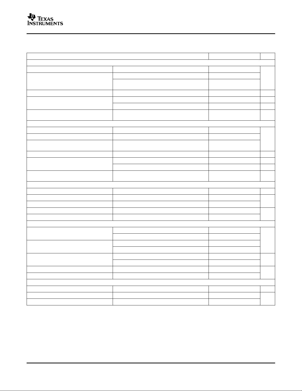
ELECTRICAL CHARACTERISTICS (continued)
over operating free-air temperature range, V
PARAMETER TEST CONDITIONS MIN TYP MAX UNIT
V
OCLoff
V
R(trip)
V
ZC
POWERGOOD COMPARATOR
V
TH(PG)
I
PG(MAX
T
PGDEL
UNDERVOLTAGE and OVERVOLTAGE PROTECTION
V
OVP
T
OVPDEL
V
UVP
T
UVPDEL
THERMAL SHUTDOWN
T
SDN1
OCP Comparator Offset -10 0 10
Current limit threshold setting
range
Zero cross detection Comparator
offset
PGOOD Threshold
PGOOD Sink Current PGOOD=0.5 V 2.5 5.0 mA
PGOOD Delay Timer Delay for PGOOD in, ‘clks’=HK Clock 256 clks
VFBx OVP Trip Threshold OVP detect 110% 115% 120%
VFBx OVP Delay Time 2ms
VFBx UVP Trip Threshold
VFBx UVP Delay Timer ‘clks’=HK Clock 128 clks
Thermal shutdown threshold °C
=12V,V
VIN
(V
VREG5-CS-VPGND-LL
R
DS(ON)
V
V5FILT-VCS
V
PGNDx-VLLx
VREG5=VV5FILT
sense
voltage 30 150 mV
voltage, SKIPSEL=0V -5 1 5
Power Bad Threshold ±7% ±10% ±13%
Hysteresis ±5%
UVP detect 65% 70% 75%
Hysteresis 6%
Shutdown temperature 145
Hysteresis 10
) voltage, V
SLUS670A–JULY 2005–REVISED AUGUST 2005
= 5 V (unless otherwise noted)
VREG5-CS
= 80mV,
7
www.ti.com
TPS51120
SLUS670A–JULY 2005–REVISED AUGUST 2005
DEVICE INFORMATION
TERMINAL FUNCTIONS
TERMINAL
NAME NO.
COMP1 2 O
COMP2 7 O
CS1 23 I
CS2 18 I
DRVH1 27 O
DRVH2 14 O
DRVL1 25 O
DRVL2 16 O
EN1 29 I
EN2 12 I
EN3 10 I
EN5 9 I
GND 5 I Signal ground pin.
LL1 26 I/O
LL2 15 I/O
PGND1 24 I/O Ground return for rectifying MOSFET gate driver. Connect PGND2, PGND1 and GND strongly together near
PGND2 17 I/O
PGOOD1 30 O Power-good window comparator open drain output. Pull up with resistor to V5FILT or appropriate signal
PGOOD2 11 O
SKIPSEL 32 I Skip and fault mode selection pin. Refer to Table 2
TONSEL 31 I On-time selection pin. Refer to Table 1 and Table 2.
V5FILT 20 I 5-V supply input for the entire control circuit. Should be provided from VREG5 via RC filter.
VBST1 28 I Supply Input for High-side MOSFET Driver. Connect capacitor from this pin to respective LL terminal. An
VBST2 13 I
VFB1 3 I
VFB2 6 I
VIN 22 I Supply Input for 5-V and 3.3-V linear regulator. Typically connected to VBAT.
VO1 1 I These terminals serve four functions: on-time adjustment, output discharge, VREG5, VREG3 switchover input
VO2 8 I
VREF2 4 O
VREG3 19 O
VREG5 21 O supply. Internally connected to VBST and DRVL. Shuts off with EN5. Switches over to VO1 when 4.8 V or
I/O DESCRIPTION
Loop compensation pin (error amplifier output). Connect RC from this pin to GND for proper loop compensation
with current mode operation. Tie this pin to V5FILT for D-CAP™ mode operation.
Current sense comparator input (-) for resistor sensing scheme. Or, overcurrent trip setting input for R
current sense scheme if connected to V5FILT through the threshold setting resistor.
High-side MOSFET gate drive output. Source 3.5 Ω, sink 1.5 Ω, LL-node referenced floating driver. Drive
voltage corresponds to VBST to LL voltage.
Rectifying (low-side) MOSFET gate drive output. Source 3.5 Ω, sink 1.5 Ω, PGND referenced driver. Drive
voltage is VREG5 voltage.
Channel 1 and Channel 2 SMPS enable pins. Connect to 5 V to turn on with internal 3-ms soft-start. Slower
soft-start is possible by applying an external capacitor from each of these pins to ground to program ramp rate.
VREG3, 3.3-V low dropout linear regulator enable pin. Connect to GND to disable. Float or tie to enabled
VREG5 to turn on the regulator.
VREG5, 5-V low dropout linear regulator enable pin. Connect to GND to disable. Float or tie to VBAT to turn on
the regulator.
High-side MOSFET gate driver return. Also serve as current sense comparator input (-) for R
input voltage monitor for on-time control circuitry
the source of the rectifying FET or the GND connection of the current sense resistor. Also serve as current
sense comparator input (+).
voltage. Current capability is 5-mA. PGOOD goes high 1-ms after VFB is within specified limits. Power bad
(terminal goes low) is within 10 µs.
internal PN diode is connected between VREG5 to each of these pins. User can add external schottky diode if
forward drop is critical to drive the power MOSFET.
SMPS feedback input. Connect the feedback resistor divider here for adjustable outputs. Tie these pins to
V5FILT or for fixed output option. Refer to Table 2
and feedback inputs for 5-V, 3.3-V fixed-output option. Connect to positive terminal of respective switch mode
power supply’s output capacitor.
2-V reference output. Capable of ±50-µA, ±2% over 0 - 85°C temperature range. Bypass to GND by 1-nF
ceramic capacitor. Tie this pin to GND disables both SMPS.
3.3-V, 100-mA low dropout linear regulator output. Bypass to PGND by 10-µF ceramic capacitor. Runs from
VIN supply. Shuts off with EN3. Switches over to VO2 when 3.1 V or above is provided.
5-V, 100-mA low dropout linear regulator output. Bypass to PGND by 10-µF ceramic capacitor. Runs from VIN
above is provided.
DS(on)
DS(on)
sensing, and
8
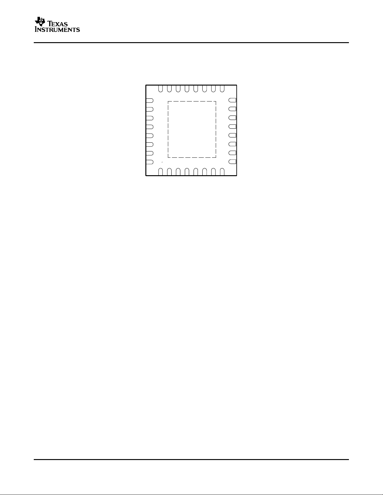
TPS51120
www.ti.com
SKIPSEL
TONSEL
PGOOD1
EN1
VBST1
DRVH1
LL1
DRVL1
QFN PACKAGE
(BOTTOM VIEW)
VO1
COMP1
VFB1
VREF2
GND
VFB2
COMP2
12345678
32
31
30
29
28
27
26
25
24 23 22 21 20 19 18 17
VIN
CS1
PGND1
VREG5
V5FILT
CS2
VREG3
VO2
9
10
11
12
13
14
15
16
PGND2
SLUS670A–JULY 2005–REVISED AUGUST 2005
EN5
EN3
PGOOD2
EN2
VBST2
DRVH2
LL2
DRVL2
9
www.ti.com
TPS51120
SLUS670A–JULY 2005–REVISED AUGUST 2005
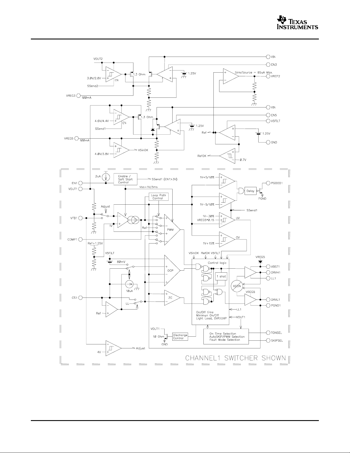
BLOCK DIAGRAM (One Channel Only Shown)
10

TPS51120
www.ti.com
SLUS670A–JULY 2005–REVISED AUGUST 2005
DETAILED DESCRIPTION
PWM Operation
The switching mode power supply (SMPS) block of TPS51120 supports an adaptive on time control
pulse-width-modulation (PWM). Switching frequency is selectable from four choices for maximum efficiency
(5 V/180 kHz, 3.3 V/270 kHz), minimum component size (5 V/380 kHz, 3.3 V/580 kHz) or the other two
intermediates. The TPS51120 supports both true current mode control and D-CAP™ mode control, selectable up
to the requirements from system design. All N-channel MOSFET totem-pole architecture is employed for external
switches. The synchronous top (high-side) MOSFET is turned on, or is “SET”, at the beginning of each cycle.
This MOSFET is turned off, or is “RESET” after a constant “on-time” period which is defined by the frequency of
customer’s choice and input and output voltage ratio. The top MOSFET is turned on again if inductor current is
reduced to meet both conditions of,
1. the current level corresponds to the error amount of output voltage and,
2. below the overcurrent limit level
Repeating operation in this manner, the controller regulates the output voltage. The synchronous bottom
(low-side) or the rectifying MOSFET is turned on each cycle in the negative phase to the top MOSFET to keep
the conduction loss minimum. The rectifying MOSFET turns off on the event reverse inductor current flow is
detected. This enables seamless transition to skip mode function so that high efficiency is kept over a broad
range of load current. At the beginning of the soft start period, the rectifying MOSFET remains in the off state
until the top MOSFET is turned on for at least once.
Current Mode
The current mode scheme is a sequence of feedback control described as follows. The output voltage is
monitored at the middle point of voltage divider resistors and fed back to a transconductance amplifier. The
amplifier outputs target current level proportional to error amount between the feedback voltage and the internal
1 V reference voltage. The inductor current level is monitored during the off-cycle, when rectifying MOSFET is
turned on. The PWM comparator compares the inductor current signal with this target current level that is
indicated at the COMP pin voltage. When both signals are equal (at the valley of the current sense signal), the
comparator provides the “SET” signal to the gate driver latch. The current mode option has relatively higher
flexibility by the external compensation network provided to the COMP pin. And it is suitable for lowest ripple
design with output capacitor(s) having ultra-low ESR. More detail information about loop compensation and
parameter design can be found in the Loop Compensation and External Parts section. When sensing the
inductor current, accuracy and cost always trades off. In order to give the circuit designer a choice between
these two, TPS51120 supports both of external resistor sensing and MOSFET R
factory for current mode EVM with R
SENSE
capability.
sensing. Please contact
DS(on)
D-CAP™ Mode
The D-CAP™ mode operation is enabled by tying the COMP pin to V5FILT. In this mode, the PWM comparator
monitors the feedback voltage directly and compares the voltage with the internal 1-V reference. When both
signals are equal at the valley of the voltage sense signal, the comparator provides the “SET” signal to the top
MOSFET gate driver. Because the compensation network is implemented on the part and the output waveform
itself is used as the error signal, external circuit design is largely simplified. Another advantage of the D-CAP™
mode is its inherent fast transient response. A trade-off is a sufficient amount of ESR required in the output
capacitor. SPCAP or POSCAP is recommended. The inductor current information is still used in the D-CAP™
mode for over current protection and light load operation. Do NOT neglect current sensing design in this mode.
To summarize, the D-CAP™ mode is suitable for the lowest external component count with the fastest transient
response, but with relatively large ripple voltage. It is easy to design the loop once appropriate output capacitor
and inductor current ripple is selected. Please refer to loop compensation and parameter design in the Loop
Compensation and External Parts section for more information.
11
 Loading...