

D
Step-Down DC-DC Converter
D
Three Operation-Mode
– Heavy Load:
– Fixed Frequency PWM
– Hysteretic (User Selctable)
– Light Load:
– Skip Mode
D
4.5 V to 25 V Input Voltage Range
D
Adjustable Output Voltage Down to 1.2 V
D
95% Efficiency
D
Stand-By Control
D
Over Current Protection
D
UVLO for Internal 5 V Regulation
D
Low Standby Current . . . 0.5 mA Typical
D
TA = –40°C to 85°C
description
TPS5103
MULTIPLE MODE SYNCHRONOUS DC/DC CONTROLLER
SLVS240 – SEPTEMBER 1999
DB PACKAGE
(TOP VIEW)
1
20
SOFTSTART
INV
FB
C
R
GND
REF
COMP
PWMSKIP
STBY
2
3
4
T
5
T
6
7
8
9
10
LH
19
OUT_u
18
LL
17
OUT_d
16
OUTGND
15
TRIP
14
VCC_SENSE
13
VCC
12
VREF5
11
VREG5V_IN
The TPS5103 is a synchronous buck dc/dc controller, designed for notebook PC system power . The controller
has three user-selectable operation modes available; hysteretic mode, fixed frequency PWM control, or SKIP
control.
In high current applications, where fast transient response is advantageous for reducing bulk capacitance, the
hysteretic mode is selected by connecting the Rt pin to Vref5. Selecting the PWM/SKIP modes for less
demanding transient applications is ideal for conserving notebook battery life under light load conditions. The
device includes high-side and low-side MOSFET drivers capable of driving low Rds (on) N–channel MOSFET s.
The user-selectable overcurrent protection (OCP) threshold is set by an external TRIP pin resister in order to
protect the system. The TPS5103 is configured so that a current sense resistor is not required, improving the
operating efficiency.
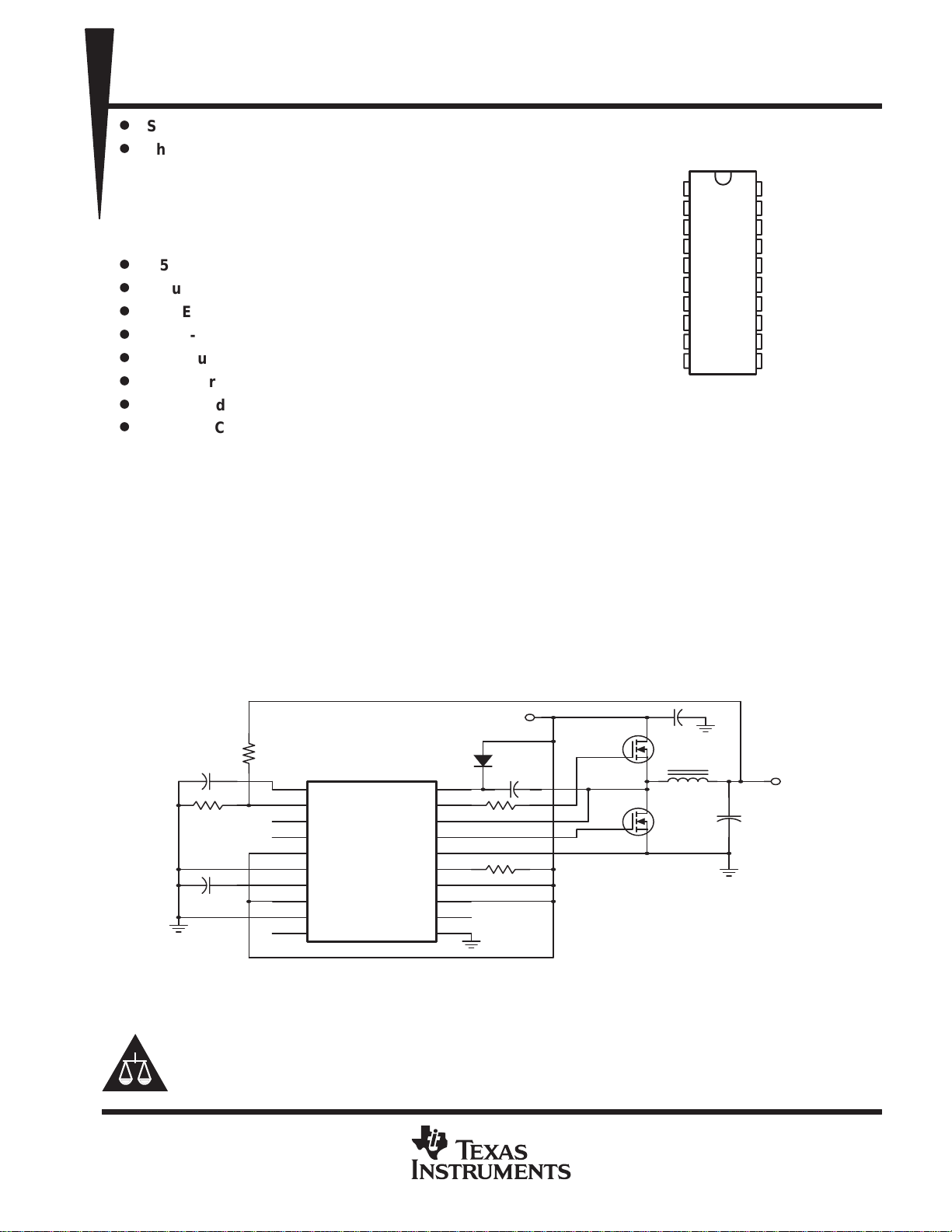
L1
C4
C5
OUTPUT
+
R2
C1
C2
R1
1
2
3
4
5
6
7
8
9
10
TPS5103
SOFTSTART
INV
FB
CT
RT
GND
REF
COMP
PWM/SKIP
STBY
U1
OUTU
OUTD
OUTGND
VCCSENSE
VREF5
VREG5V_IN
LH
LL
TRIP
VCC
5 V
D1
20
19
18
17
16
15
14
13
12
11
C3
R3
R4
Q1
Q2
Please be aware that an important notice concerning availability, standard warranty, and use in critical applications of
Texas Instruments semiconductor products and disclaimers thereto appears at the end of this data sheet.
TI is a trademark of Texas Instruments Incorporated.
PRODUCT PREVIEW information concerns products in the formative or
design phase of development. Characteristic data and other
specifications are design goals. Texas Instruments reserves the right to
change or discontinue these products without notice.
POST OFFICE BOX 655303 • DALLAS, TEXAS 75265
Figure 1. Typical Design
Copyright 1999, Texas Instruments Incorporated
1
TPS5103
T
°C
MULTIPLE MODE SYNCHRONOUS DC/DC CONTROLLER
SLVS240 – SEPTEMBER 1999
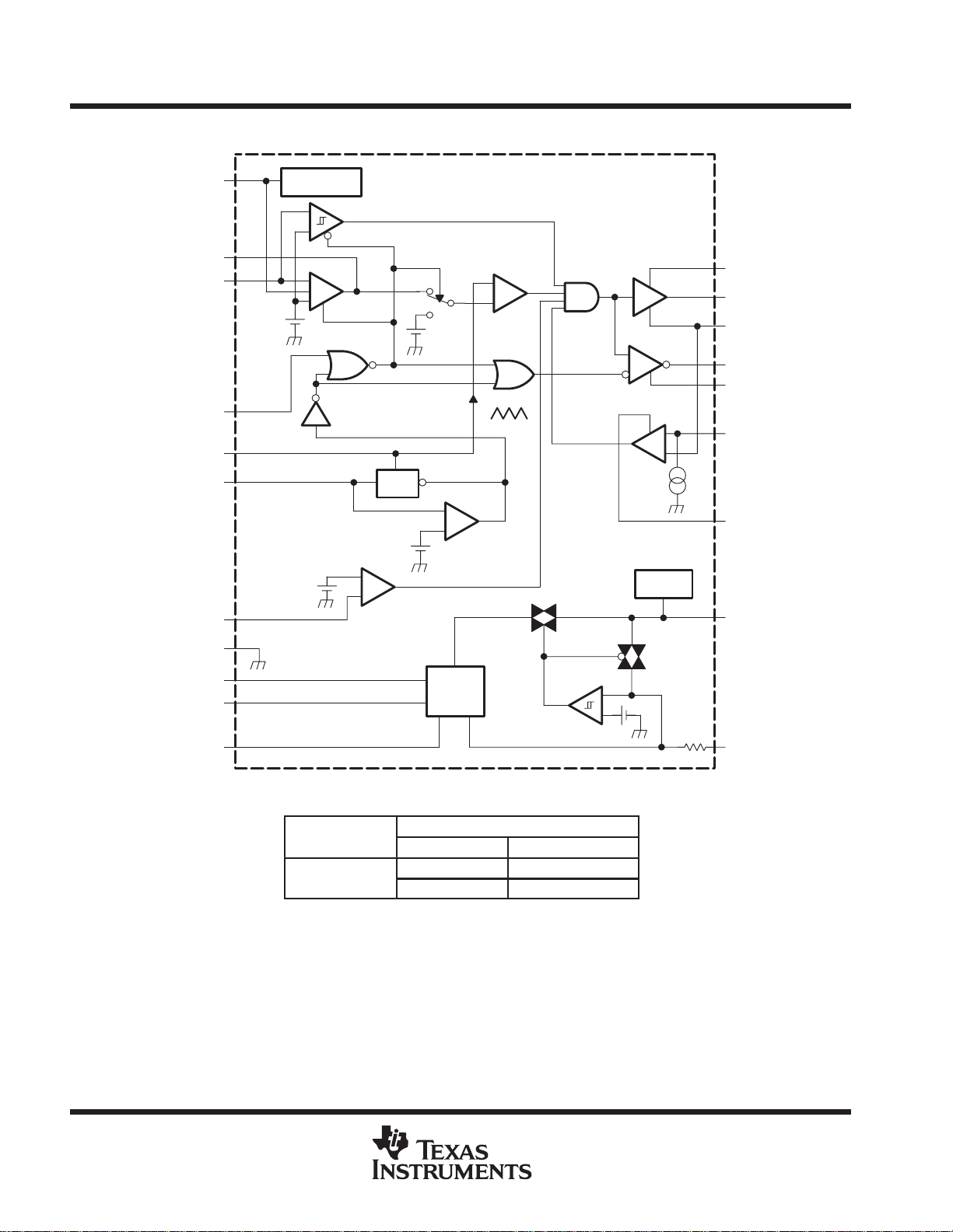
functional block diagram
SOFT START
FB
INV
PWMSKIP
C
R
Comp
T
T
1.185 V
Soft Start
1.185 V
_
+
_
+
Error Amp
PWM Comp.
_
+
One Shot ON
_
+
OSC
_
+
Disable
_
+
UVLO
LH
OUT_u
LL
OUT_d
OUTGND
TRIP
VCC_SENSE
VREF5
GND
V
CC
STBY
REF
1.185 V
°
–40 °C to 85
VREF
AVAILABLE OPTIONS
A
°
SSOP(DB) EVM
TPS5103IDB TPS5103EVM–136
TPS5103IDBR
PACKAGE
_
+
VREG5V_IN
2
POST OFFICE BOX 655303 • DALLAS, TEXAS 75265
I/O
DESCRIPTION
MULTIPLE MODE SYNCHRONOUS DC/DC CONTROLLER
Terminal Functions
TERMINAL
NAME NO.
COMP 8 I Comparator input for voltage monitor
C
T
FB 3 O Feedback output of error amp
GND 6 Control GND
INV 2 I Inverting input of both error amp and hysteretic comparator
LH 20 I/O Bootstrap. Connect 1 µF low-ESR capacitor from LH to LL.
LL 18 I/O
OUT_d 17 I/O Gate-drive output for low-side power switching FET s
OUTGND 16 Ground for FET drivers
OUT_u 19 O Gate-drive output for high-side power switching FET s
PWMSKIP 9 I
REF 7 O 1.185-V reference voltage output
R
T
SOFTSTAR T 1 I External capacitor from SOFTST ART to GND for soft start control
STBY 10 I Standby control
TRIP 15 I External resistor connection for output current control
V
CC
VCC_SENSE 14 I Supply voltage sense for current protection
VREF5 12 O 5-V-internal regulator output
VREG5V_IN 11 I External 5-V input (input voltage range = 4.5 V to 25 V)
4 I/O
5 I/O External resistor connection for adjusting the triangle oscillator.
13 I Supply voltage input
External capacitor from CT to GND for adjusting the triangle oscillator and decreasing the current limiting
voltage
Bootstrap low. High side gate driving return and output current protection. Connect to the junction of the high
side and low side FETs for floating drive configuration.
PWM/SKIP mode select
L:PWM mode
H:SKIP mode
TPS5103
SLVS240 – SEPTEMBER 1999
POST OFFICE BOX 655303 • DALLAS, TEXAS 75265
3

TPS5103
MULTIPLE MODE SYNCHRONOUS DC/DC CONTROLLER
SLVS240 – SEPTEMBER 1999
detailed description
REF
The reference voltage is used for the output voltage setting and the voltage protection(COMP). The tolerance
is 1.5% typically.
VREF5
An internal linear voltage regulator is used for the high-side driver bootstrap voltage. Since the input voltage
range is from 4.5 V to 25 V, this voltage offers a fixed voltage for the bootstrap voltage so that the design for
the bootstrap is much easier. The tolerance is 6%.
hysteretic comparator
The hysteretic comparator is used to regulate the output voltage of the synchronous-buck converter. The
hysteresis is set internally and is typically 9.7 mV. The total delay time from the comparator input to the driver
output is typically 400 ns for going both high and low.
error amplifier
The error amplifier is used to sense the output voltage of the synchronous buck converter. The negative input
of the error amplifier is connected to the Vref voltage(1.185 V) with a resistive divider network. The output of
the error amplifier is brought out to the FB terminal to be used for loop gain compensation.
low-side driver
The low-side driver is designed to drive low-Rds(on) n-channel MOSFETs. The maximum drive voltage is 5 V
from VREF5. The current rating of driver is typically 1.2 A at sink current, –1.5 A at source current.
high-side driver
The high-side driver is designed to drive low-Rds(on) n-channel MOSFETs. The current rating of the driver is
1.2 A at sink current, –1.7 A at source current. When configured as a floating driver, the bias voltage to the driver
is developed from the VREF5, limiting the maximum drive voltage between OUT_u and LL to 5 V . The maximum
voltage that can be applied between LH and OUTGND is 30 V.
driver deadtime control
The deadtime control prevents shoot-through current from flowing through the main power FETs. During
switching transitions the
deadtime from the low-side-driver-off to the high-side-driver-on is 90 ns, and 110 ns from high-side-driver-off
to low-side-driver-on.
COMP
COMP is designed for use with a regulation output monitor. COMP also functions as an internal comparator
used for any voltage protection such as the input under voltage protection. If the input voltage is lower than the
setpoint, the comparator turns off and prevents external parts from damage. The investing terminal of the
comparator is internally connected to REF(1.185 V).
current protection
Current protection is achieved by sensing the high-side power MOSFET drain-to-source voltage drop during
on-time through VCC_SENSE and LL terminals. An external resistor between Vin and TRIP terminal with the
internal current source connected to the current comparator negative input adjusts the current limit. The typical
internal current source value is 15 µA in PWM mode, 5 µA in SKIP mode. When the voltage on the positive
terminal is lower than the negative terminal, the current comparator turns on the trigger, and then activates the
oscillator. This oscillator repeatedly reset the trigger until the over current condition is removed. The capacitor
on the C
terminal can be open or added to adjust the reset frequency.
T
deadtime control actively controls the turnon time of the MOSFET drivers. The typical
4
POST OFFICE BOX 655303 • DALLAS, TEXAS 75265
MULTIPLE MODE SYNCHRONOUS DC/DC CONTROLLER
SLVS240 – SEPTEMBER 1999
detailed description (continued)
softstart
SOFTST ART sets the sequencing of the output for any possibility. The capacitor value for a start-up time can
be calculated by the following equation: C = 2xT (uF) where C is the external capacitor value, T is the required
start-up time in (ms).
standby
This controller can be switched into standby mode by grounding the STBY terminal. When it is in standby mode,
the quiescent current is less than 1.0 uA.
UVLO
The under-voltage-lock-out (ULVO) threshold is approximately 3.8 V. The typical hysteresis is 55 mV.
5-V Switch
5-V Switch if the internal 5-V switch senses a 5-V input from REG5V terminal, the internal 5-V linear regulator
will be disconnected from the MOSFET drivers. The external 5 V will be used for both the low-side driver and
the high-side bootstrap, thus increasing the efficiency.
PWM/SKIP switch
TPS5103
The PWM/SKIP switch selects the output operating mode. This controller has three operational modes, PWM,
SKIP, and Hysteretic. The PWM and SKIP mode control should be used for slower transient applications.
oscillator
The oscillator gives a triangle wave by connecting an external resistor to the R
terminal and an external
T
capacitor to the CT terminal. The voltage amplitude is 0.43 V ~ 1.17 V. This wave is connected to the noninverting input of the PWM comparator.
Comparison Table Between PWM Mode and Hysteretic Mode
MODE PWM HYSTERETIC
Frequency Fixed Not Fixed
Transient Response Normal Very fast
Feed back compensation Need Needless
POST OFFICE BOX 655303 • DALLAS, TEXAS 75265
5
TPS5103
VIInput voltage
V
MULTIPLE MODE SYNCHRONOUS DC/DC CONTROLLER
SLVS240 – SEPTEMBER 1999
absolute maximum ratings over operating free-air temperature (unless otherwise noted)
†
Supply voltage, VCC (see Note 1) –0.3 V to 27 V. . . . . . . . . . . . . . . . . . . . . . . . . . . . . . . . . . . . . . . . . . . . . . . . . . .
Input voltage, VI, INV, CT, RT, PWM/SKIP, SOFTSTART, COMP –0.3 V to 7 V. . . . . . . . . . . . . . . . . . . . . . . . . .
Input voltage, VREG5V_IN –0.3 V to 6 V. . . . . . . . . . . . . . . . . . . . . . . . . . . . . . . . . . . . . . . . . . . . . . . . . . . . . . . . . .
Input voltage, STBY –0.3 V to 15 V. . . . . . . . . . . . . . . . . . . . . . . . . . . . . . . . . . . . . . . . . . . . . . . . . . . . . . . . . . . . . . .
Input voltage, TRIP, VCC_SENSE –0.3 V to 27 V. . . . . . . . . . . . . . . . . . . . . . . . . . . . . . . . . . . . . . . . . . . . . . . . . . .
Output current, I
3 A. . . . . . . . . . . . . . . . . . . . . . . . . . . . . . . . . . . . . . . . . . . . . . . . . . . . . . . . . . . . . . . . . . . . . . . . . .
O
Low level output voltage, VOL –0.3 V to 27 V. . . . . . . . . . . . . . . . . . . . . . . . . . . . . . . . . . . . . . . . . . . . . . . . . . . . . .
High level output voltage, V
Reference voltage, V
–0.3 V to 3 V. . . . . . . . . . . . . . . . . . . . . . . . . . . . . . . . . . . . . . . . . . . . . . . . . . . . . . . . . . . . .
ref
–0.3 V to 32 V. . . . . . . . . . . . . . . . . . . . . . . . . . . . . . . . . . . . . . . . . . . . . . . . . . . . . .
OH
Operating free-air temperature range, TA –40°C to 85°C. . . . . . . . . . . . . . . . . . . . . . . . . . . . . . . . . . . . . . . . . . . .
Operating virtual junction temperature range, TJ –125°C. . . . . . . . . . . . . . . . . . . . . . . . . . . . . . . . . . . . . . . . . . . .
Storage temperature range, T
†
Stresses beyond those listed under “absolute maximum ratings” may cause permanent damage to the device. These are stress ratings only, and
functional operation of the device at these or any other conditions beyond those indicated under “recommended operating conditions” is not
implied. Exposure to absolute-maximum-rated conditions for extended periods may affect device reliability.
NOTES: 1. All voltage values are with respect to the network ground terminal.
2. See Dissipation Rating Table for free-air temperature range above 25°C.
PACKAGE
DB 801 mW 6.408mW/ °C 416 mW
–55°C to 150°C. . . . . . . . . . . . . . . . . . . . . . . . . . . . . . . . . . . . . . . . . . . . . . . . . . .
stg
DISSIPATION RATING TABLE
TA ≤ 25°C
POWER RATING
DERATING FACTOR
ABOVE TA = 25°C
TA = 85°C
POWER RATING
recommended operating conditions
MIN NOM MAX UNIT
V
CC
R
T
C
T
f Frequency 200 kHz
T
A
‡
Not a JEDEC symbol.
Supply voltage 4.5 25 V
INV, CT, RT, COMP, PWM_SKIP, SOFTSTART 6
p
‡
‡
Oscillator frequency
Operating temperature range –40 85 °C
VREG5V_IN 5.5
STBY 12
TRIP, VCC_SENCE 25
Timing register 82 kΩ
Timing capacitor 100 pF
6
POST OFFICE BOX 655303 • DALLAS, TEXAS 75265
V
Reference voltage
V
Frequency change
†
V
‡
High-level output voltage
V
V
‡
Low-level output voltage
V
V
High-level input voltage
V
V
Low-level input voltage
V
TPS5103
MULTIPLE MODE SYNCHRONOUS DC/DC CONTROLLER
SLVS240 – SEPTEMBER 1999
electrical characteristics over recommended operating free-air temperature range, VCC = 7 V
(unless otherwise noted)
reference voltage
PARAMETER TEST CONDITIONS MIN TYP MAX UNIT
ref
Regin Line regulation
Regl Load regulation
†
Not a JEDEC symbol.
†
†
TA = 25°C, I
= 50 µA
‡
I
vref
VCC = 4.5 V to 25 V, I = 50 µA 0.2 12 mV
I = 1 µA to 1 mA 0.5 10 mV
oscillator
PARAMETER TEST CONDITIONS MIN TYP MAX UNIT
f Frequency PWM mode 500 kHz
R
T
fdv
fdt
HL
LL
†
Not a JEDEC symbol.
‡
The output voltages of oscillator (f = 200 kHz) are ensured by design.
Timing resistor 47 kΩ
VCC = 4.5 V to 25 V 0.1%
TA = –40°C to 85°C 2%
p
p
DC includes internal comparator error 1 1.1 1.2
f = 200 kHz, includes internal comparator error 1.17
DC includes internal comparator error 0.4 0.5 0.6
f = 200 kHz, includes internal comparator error 0.43
= 50 µA 1.167 1.185 1.203
vref
1.155 1.215
error amp
PARAMETER TEST CONDITIONS MIN TYP MAX UNIT
V Input offset voltage TA = 25°C 2 10 mV
Av Open-loop voltage gain
GB Unity-gain bandwidth
I
O
I
S
†
Not a JEDEC symbol.
Output sink current VO = 0.4 V 30 45 µA
Output source current VO = 1 V 300 µA
hysteresis comparator
PARAMETER TEST CONDITIONS MIN TYP MAX UNIT
V
hsy
Vp-VSOffset voltage 2 mV
I Bias current 10 pA
t
PHL
t
PLH
§
The numbers in the table include the driver delay. All numbers are ensured by design.
Hysteresis window Hysteretic mode 6 9.7 13 mV
Propagation delay from INV to OUT_U TTL input signal 230 ns
†
†
50 dB
0.8 MHz
§
10 mV overdrive on hysteresis band signal 400 ns
control
PARAMETER TEST CONDITIONS MIN TYP MAX UNIT
IHA
ILA
p
p
STBY 2.5
PWM_SKIP 2
STBY 0.5
PWM_SKIP 0.5
POST OFFICE BOX 655303 • DALLAS, TEXAS 75265
7
TPS5103
Threshold voltage
†
V
Threshold voltage
†
V
I
TRIP terminal current
A
MULTIPLE MODE SYNCHRONOUS DC/DC CONTROLLER
SLVS240 – SEPTEMBER 1999
electrical characteristics over recommended operating free-air temperature range, VCC = 7 V
(unless otherwise noted) (continued)
5-V regulator
PARAMETER TEST CONDITIONS MIN TYP MAX UNIT
V
O
Regin Line regulation
Regl Load regulation
I
OS
†
Not a JEDEC symbol.
5-V switch
V
IT(high)
V
IT(low)
V
hsy
†
Not a JEDEC symbol.
UVLO
V
IT(high)
V
IT(low)
V
hys
†
Not a JEDEC symbol.
Output voltage I = 10 mA 4.7 5.3 V
†
†
Short-circuit output current V
PARAMETER TEST CONDITIONS MIN TYP MAX UNIT
Hysteresis) 50 150 250 mV
PARAMETER TEST CONDITIONS MIN TYP MAX UNIT
Hysteresis 10 150 mV
VCC = 5.5 V to 25 V, I = 10 mA 20 mV
I = 1 mA to 10 mA, VCC = 5.5 V 40 mV
= 0 V 70 mA
ref
4.2 4.9
4.1 4.8
3.6 4.2
3.5 4.1
output
I
O
I
S
I
O
I
S
t
r
t
f
PARAMETER TEST CONDITIONS MIN TYP MAX UNIT
OUT_u sink curent VO = 3 V 0.5 1.2 A
OUT_u source current VO = 2 V –1 –1.7 A
OUT_d sink current VO = 3 V 0.5 1.2 A
OUT_d source current VO = 2 V –1 –1.5 A
PWM mode, VTRIP = 7 V 10 15 20
SKIP mode, VTRIP = 7 V 3 5 7
High side driver is GND referenced.
Input: INV = 0 – 3V
Rise time
Fall time
tr/tf = 10 ns,
CL = 2200 pF 28
CL = 3300 pF 39
High side driver is GND referenced.
Input: INV = 0 – 3 V
tr/tf = 10 ns,
CL = 2200 pF 30
CL = 3300 pF 38
Frequency = 200 kHz
Frequency = 200 kHz
µ
ns
ns
8
POST OFFICE BOX 655303 • DALLAS, TEXAS 75265
†
V
TPS5103
MULTIPLE MODE SYNCHRONOUS DC/DC CONTROLLER
SLVS240 – SEPTEMBER 1999
electrical characteristics over recommended operating free-air temperature range, VCC = 7 V
(unless otherwise noted) (continued)
softstart
PARAMETER TEST CONDITIONS MIN TYP MAX UNIT
I
(CTRL)
V
IT(high)
V
IT(low)
†
Not a JEDEC symbol.
output voltage monitor
V
IT
driver deadtime section
T
DRVLH
T
DRVHL
whole device
I
CC
I Shutdown current STBY = 0 V 0.01 10 µA
Softstart current 1.9 2.5 3 µA
Threshold voltage (SKIP mode)
PARAMETER TEST CONDITIONS MIN TYP MAX UNIT
Threshold voltage 1.08 1.18 1.28 V
PARAMETER TEST CONDITIONS MIN TYP MAX UNIT
Low-side to high-side 90 ns
High-side to low-side 110 ns
PARAMETER TEST CONDITIONS MIN TYP MAX UNIT
Supply current 0.5 1.2 mA
3.9
2.6
0.1 µF
5V
SOFTSTART
INV
FB
C
T
R
T
GND
VCC_SENSE
REF
COMP
PWM SKIP
STBY
OUTGND
TRIP
VCC
VREF5
5V_IN
Figure 2. Test Circuit
LH
OUT_u
LL
OUT_d
0.1 µF
7V
POST OFFICE BOX 655303 • DALLAS, TEXAS 75265
9
TPS5103
MULTIPLE MODE SYNCHRONOUS DC/DC CONTROLLER
SLVS240 – SEPTEMBER 1999
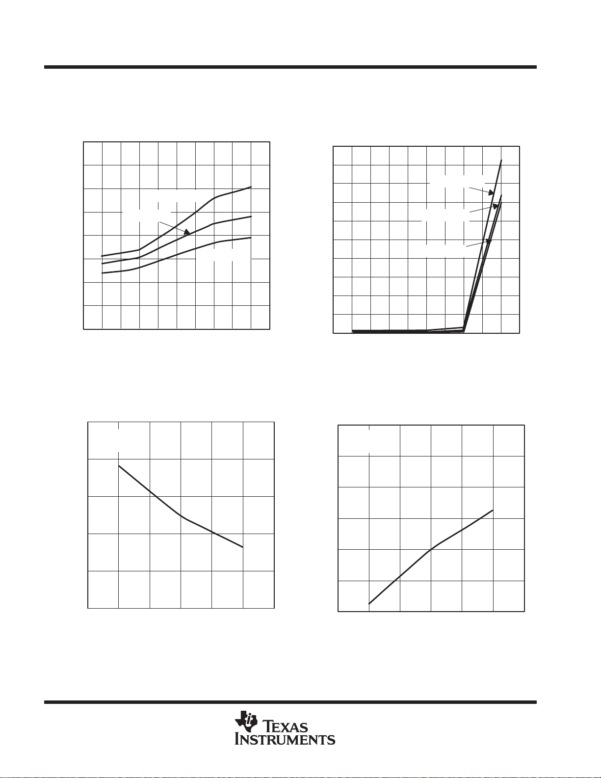
TYPICAL CHARACTERISTICS
QUIESCENT CURRENT
JUNCTION TEMPERATURE
700
650
Aµ
600
550
500
450
– Quiescent Current –
400
CC
I
350
300
–40 –20 25
TJ – Junction Temperature – °C
DRIVE OUTPUT VOLTAGE
5.5
VCC = 7 V,
TJ = 25°C
5
vs
VCC = 25 V
VCC = 7 V
Figure 3
vs
DRIVE CURRENT
VCC = 4.5 V
85 125
QUIESCENT CURRENT
JUNCTION TEMPERATURE
50
45
Aµ
40
35
30
25
20
– Quiescent Current –
15
CCS
I
10
5
0
–40 –20 25
TJ – Junction Temperature – °C
DRIVE OUTPUT VOLTAGE
3
VCC = 7 V,
TJ = 25°C
2.5
vs
VCC = 25 V
VCC = 7 V
VCC = 4.5 V
85 125
Figure 4
vs
DRIVE CURRENT
10
4.5
– Drive Output Voltage – VV
3.5
(OUT_u)
4
3
0.1 0.7
I
(OUT_source)
– Drive Source Current – A
Figure 5
2
1.5
1
– Drive Output Voltage – VV
(OUT_u)
0.5
1
POST OFFICE BOX 655303 • DALLAS, TEXAS 75265
0
0.1 0.7
I
(OUT_sink)
– Drive Source Current – A
Figure 6
1
TPS5103
MULTIPLE MODE SYNCHRONOUS DC/DC CONTROLLER
SLVS240 – SEPTEMBER 1999
TYPICAL CHARACTERISTICS
– Drive Output Voltage – VV
(OUT_d)
1.125
DRIVE OUTPUT VOLTAGE
vs
DRIVE CURRENT
6
TJ = 25°C
5
4
3
2
1
0
0.1 0.7
I
(OUT_source)
– Drive Source Current – A
Figure 7
OSCILLATOR OUTPUT VOLTAGE
vs
JUNCTION TEMPERATURE
DRIVE OUTPUT VOLTAGE
vs
DRIVE CURRENT
4.5
TJ = 25°C
4
3.5
3
2.5
2
– Drive Output Voltage – VV
1.5
1
(OUT_d)
0.5
1
0
0.1 0.7
I
(OUT_sink)
– Drive Source Current – A
1
Figure 8
OSCILLATOR OUTPUT VOLTAGE
vs
JUNCTION TEMPERATURE
500
1.115
1.105
1.095
– Oscillator Output Voltage – V
1.085
(osch)
V
1.075
VCC = 4.5 V,
VCC = 7 V,
VCC = 25 V
–40 –20 25
TJ – Junction Temperature – °C
Figure 9
85 125
495
490
– Oscillator Output Voltage – V
485
(oscl)
V
480
VCC = 4.5 V,
VCC = 7 V,
VCC = 25 V
–40 –20 25
TJ – Junction Temperature – °C
Figure 10
85 125
POST OFFICE BOX 655303 • DALLAS, TEXAS 75265
11
TPS5103
MULTIPLE MODE SYNCHRONOUS DC/DC CONTROLLER
SLVS240 – SEPTEMBER 1999
TYPICAL CHARACTERISTICS
ERROR AMPLIFIER INPUT OFFSET VOLTAGE
vs
JUNCTION TEMPERATURE
2.5
2
VCC = 4.5 V,
VCC = 7 V,
1.5
VCC = 25 V
1
0.5
– Error Amplifier Input Offset Voltage – mV
io
V
0
–40 –20 25
TJ – Junction Temperature – °C
85 125
Figure 11
ERROR AMPLIFIER OUTPUT VOLTAGE
vs
JUNCTION TEMPERATURE
6.2
6
5.8
5.6
5.4
5.2
VCC = 4.5 V,
VCC = 7 V,
VCC = 25 V
ERROR AMPLIFIER OUTPUT VOLTAGE
vs
JUNCTION TEMPERATURE
2.5
2
VCC = 4.5 V,
VCC = 7 V,
1.5
1
– Error Amplifier Output V oltage – mV
0.5
om+
V
0
VCC = 25 V
–40 –20 25
TJ – Junction Temperature – °C
85 125
Figure 12
HYSTERESIS COMPARATOR HYSTERESIS VOLTAGE
vs
JUNCTION TEMPERATURE
10.5
VCC = 7 V
10.25
10
9.75
4.8
– Error Amplifier Output V oltage – mV
om–
4.6
V
4.4
12
5
–40 –20 25
TJ – Junction Temperature – °C
Figure 13
9.5
9.25
– Hysteresis Comparator Hysteresis Voltage – mV
hys
9
85 125
POST OFFICE BOX 655303 • DALLAS, TEXAS 75265
V
–40 –20 25 85 125
TJ – Junction Temperature – °C
Figure 14
TPS5103
MULTIPLE MODE SYNCHRONOUS DC/DC CONTROLLER
SLVS240 – SEPTEMBER 1999
TYPICAL CHARACTERISTICS
2.5
2
1.5
1
0.5
– Standby Switch Threshold Voltage – V
IL
V
IH,
V
0
6
STANDBY SWITCH THRESHOLD VOLTAGE
vs
JUNCTION TEMPERATURE
VCC = 4.5 V,
VCC = 7 V
VCC = 25 V
VCC = 25 V
VCC = 4.5 V
VCC = 7 V
–45 –25 25
TJ – Junction Temperature – °C
95 135
Figure 15
VREF5 OUTPUT VOLTAGE
vs
OUTPUT CURRENT
VREF5 OUTPUT VOLTAGE
SUPPLY VOLTAGE
5.2
5.1
5
4.9
4.8
4.7
4.6
4.5
– VREF5 Output Voltage – V
O
V
4.4
4.3
4.2
010
TJ = 125°C
VCC – Supply Voltage – V
Figure 16
VREF5 SHORT CURRENT
JUNCTION TEMPERATURE
–100
vs
TJ = –40°C
TJ = 25°C
20
vs
5
4
3
2
– VREF5 Output Voltage – V
O
V
1
0
TJ = 125°C
TJ = 25°C
TJ = –40°C
0 –10 –20 –30 –40
IO – Output Current – mA
Figure 17
–50 –60 –70
VCC = 25 V
–80
–60
VCC = 4.5 V
–40
– VREF5 Short Current – mA
–20
OS
I
0
–40 –20 25
TJ – Junction Temperature – °C
Figure 18
VCC = 7 V
85 125
POST OFFICE BOX 655303 • DALLAS, TEXAS 75265
13
TPS5103
MULTIPLE MODE SYNCHRONOUS DC/DC CONTROLLER
SLVS240 – SEPTEMBER 1999
TYPICAL CHARACTERISTICS
4
3.95
3.90
3.85
3.80
– UVOL Threshold Voltage – V
TLH
V
3.75
THL,
V
3.70
4.80
UVLO THRESHOLD VOLTAGE
vs
JUNCTION TEMPERATURE
V
TLH
V
THL
–40 –20 25
TJ – Junction Temperature – °C
Figure 19
5 VSW THRESHOLD VOLTAGE
vs
JUNCTION TEMPERATURE
85 125
80
70
60
50
40
30
20
– UVLO Hysteresis Voltage – mV
hys
V
10
0
200
UVLO HYSTERESIS VOLTAGE
vs
JUNCTION TEMPERATURE
–40 –20 25
TJ – Junction Temperature – °C
Figure 20
5 VSW HYSTERESIS VOLTAGE
vs
JUNCTION TEMPERATURE
85 125
4.75
4.70
4.65
4.60
4.55
– 5 VSW Threshold Voltage – V
4.50
TLH
4.45
V
THL,
4.40
V
4.35
V
TLH
V
THL
–45 –25 25
TJ – Junction Temperature – °C
Figure 21
95 135
180
160
140
120
100
80
60
– 5V SW Hysteresis Voltage – mV
40
hys
V
20
0
–45 –25 25
TJ – Junction Temperature – °C
Figure 22
95 135
14
POST OFFICE BOX 655303 • DALLAS, TEXAS 75265

TPS5103
MULTIPLE MODE SYNCHRONOUS DC/DC CONTROLLER
SLVS240 – SEPTEMBER 1999
TYPICAL CHARACTERISTICS
JUNCTION TEMPERATURE
–2.45
–2.40
Aµ
–2.35
VCC = 4.5 V
–2.30
– Softstart Current –
CTRL
–2.25
I
–2.20
–40 –20 25
TJ – Junction Temperature – °C
SOFTSTART CURRENT
vs
VCC = 7 V
VCC = 25 V
85 125
Figure 23
4.5
4
3.5
3
2.5
2
1.5
– Softstart Threshold Voltage – V
1
TLH
V
0.5
0
SOFTSTART THRESHOLD VOLTAGE
vs
JUNCTION TEMPERATURE
VCC = 7 V,
VCC = 25 V
–40 –20 25
TJ – Junction Temperature – °C
VCC = 4.5 V
85 125
Figure 24
3.5
3
2.5
2
– Softstart Threshold Voltage – V
1.5
THL
V
1
SOFTSTART THRESHOLD VOLTAGE
vs
JUNCTION TEMPERATURE
VCC = 7 V,
VCC = 25 V
VCC = 4.5 V
–40 –20 25
TJ – Junction Temperature – °C
85 125
Figure 25
1.195
1.193
1.190
1.188
1.185
Threshold Voltage – V
– Output Voltage Monitor Comparator
1.183
TH
V
1.180
OUTPUT VOLTAGE MONITOR COMPARATOR
THRESHOLD VOLTAGE
vs
JUNCTION TEMPERATURE
VCC = 4.5 V,
VCC = 7 V,
VCC = 25 V
–40 –20 25
TJ – Junction Temperature – °C
85 125
Figure 26
POST OFFICE BOX 655303 • DALLAS, TEXAS 75265
15

TPS5103
MULTIPLE MODE SYNCHRONOUS DC/DC CONTROLLER
SLVS240 – SEPTEMBER 1999
TYPICAL CHARACTERISTICS
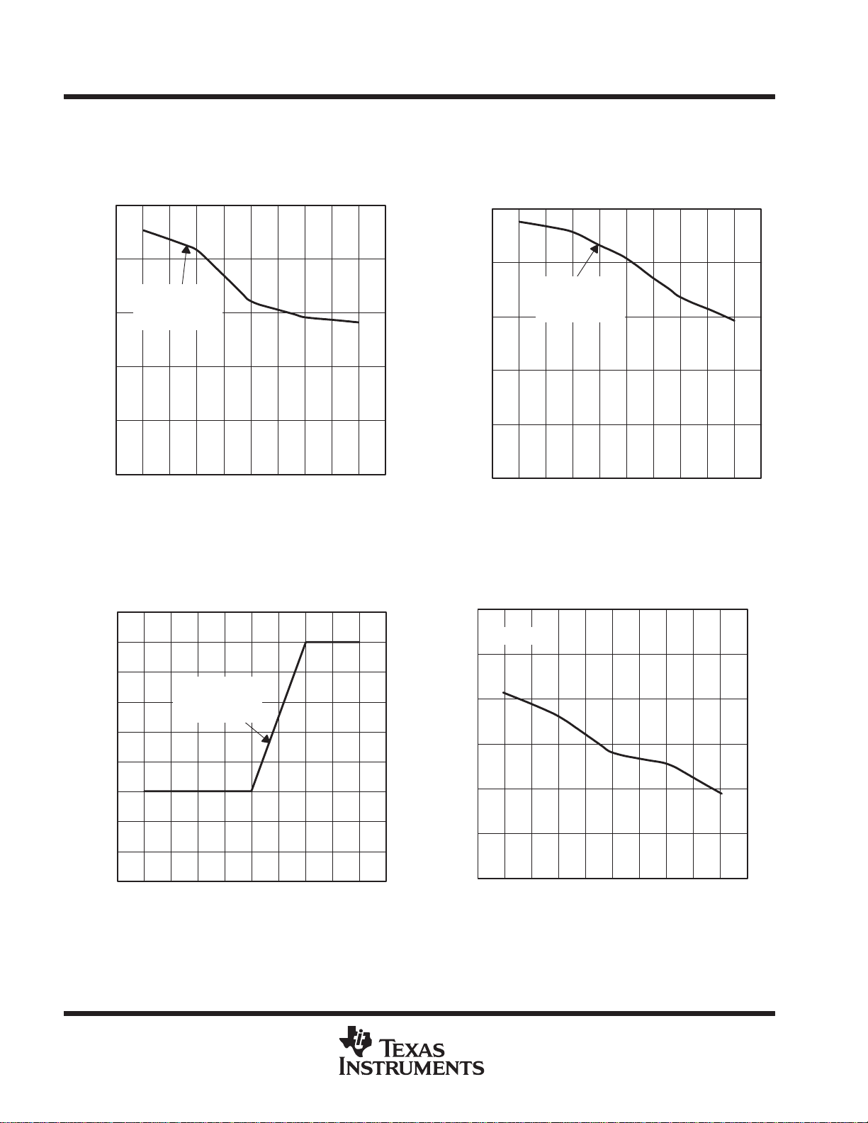
OSCILLATOR FREQUENCY
JUNCTION TEMPERATURE
600
500
400
300
200
– Oscillator Frequency – kHz
osc
F
100
0
VCC = 4.5 V,
VCC = 7 V,
VCC = 25 V
F = 200 kHz
–40 –20 25
TJ – Junction Temperature – °C
Figure 27
vs
1.6
F = 500 kHz
VCC = 4.5 V,
VCC = 7 V,
VCC = 25 V
85 125
1.4
1.2
1
0.8
0.6
– Oscillator Output Voltahe – V
0.4
OSCL
V
0.2
OSCH,
V
0
10 100
ERROR AMPLIFIER GAIN AND PHASE SHIFT
60
Rs = 100 Ω,
50
40
30
Phase
Rf = 10 kΩ
OSCILLATOR OUTPUT VOLTAGE
vs
FREQUENCY
V
OSCH
V
OSCL
F
– Frequency – kHz
OSC
Figure 28
180
140
100
1000
16
20
10
Error Amplifier Gain – dB
0
–10
–20
1.E+03 1.E+04 1.E+05
Gain
f – Frequency – Hz
Figure 29
POST OFFICE BOX 655303 • DALLAS, TEXAS 75265
1.E+06 1.E+07
60
Phase Shift – Deg
20
–20
–60

TPS5103
MULTIPLE MODE SYNCHRONOUS DC/DC CONTROLLER
SLVS240 – SEPTEMBER 1999
TYPICAL CHARACTERISTICS
MAXIMUM DUTY CYCLE
JUNCTION TEMPERATURE
100
99.5
99
98.5
98
97.5
97
96.5
Maximum Duty Cycle – %
96
95.5
95
–40 –20 25
TJ – Junction Temperature – °C
DRIVER DEAD TIME
JUNCTION TEMPERATURE
140
VCC = 4.5 V
120
T
DRVHL
vs
Figure 30
vs
f = 200 kHz
85 125
SOFTSTART CAPACITANCE
SOFTSTART TIME
4
10
3
10
2
10
– Softstart Capacitance – pF
SS
C
100
0.01 0.1 1
TSS – Soft Start Time – ms
Figure 31
CURRENT PROTECTION SOURCE CURRENT
INPUT VOLTAGE PWM MODE
14.5
Aµ
14.25
vs
10 100
vs
100
80
– Driver Dead Time – ns
60
DRVHL
T
40
DRVLH,
20
T
0
VCC = 7 V,
VCC = 25 V
VCC = 7 V,
VCC = 25 V
–45 –25 25
TJ – Junction Temperature – °C
Figure 32
T
DRVLH
VCC = 4.5 V
95 135
POST OFFICE BOX 655303 • DALLAS, TEXAS 75265
14
13.75
13.5
13.25
13
– Corrent Protection Source Current –
12.75
TRIP
I
12.5
4.5 7
TA = 125°C
TA = 25°C
TA = –40°C
V
– Input Voltage – V
TRIP
Figure 33
25
17

TPS5103
MULTIPLE MODE SYNCHRONOUS DC/DC CONTROLLER
SLVS240 – SEPTEMBER 1999
TYPICAL CHARACTERISTICS
CURRENT PROTECTION SOURCE CURRENT
vs
INPUT VOLTAGE SKIP MODE
4.6
Aµ
TA = 125°C
4.5
4.4
TA = 25°C
4.3
4.2
– Corrent Protection Source Current –
4.1
TRIP
I
4
4.5 7
TA = –40°C
V
– Input Voltage – V
TRIP
Figure 34
OSCILLATOR FREQUENCY
vs
RESISTOR
700
600
500
400
300
CT = 22 pF
CT = 33 pF
25
CT = 10 pF
CT = 15 pF
18
– Oscillator Frequency – kHzF
200
osc
100
0
CT = 470 pF
10 100
POST OFFICE BOX 655303 • DALLAS, TEXAS 75265
CT = 680 pF
1000
RT – Resistor – kΩ
Figure 35
MULTIPLE MODE SYNCHRONOUS DC/DC CONTROLLER
SLVS240 – SEPTEMBER 1999
APPLICATION INFORMATION
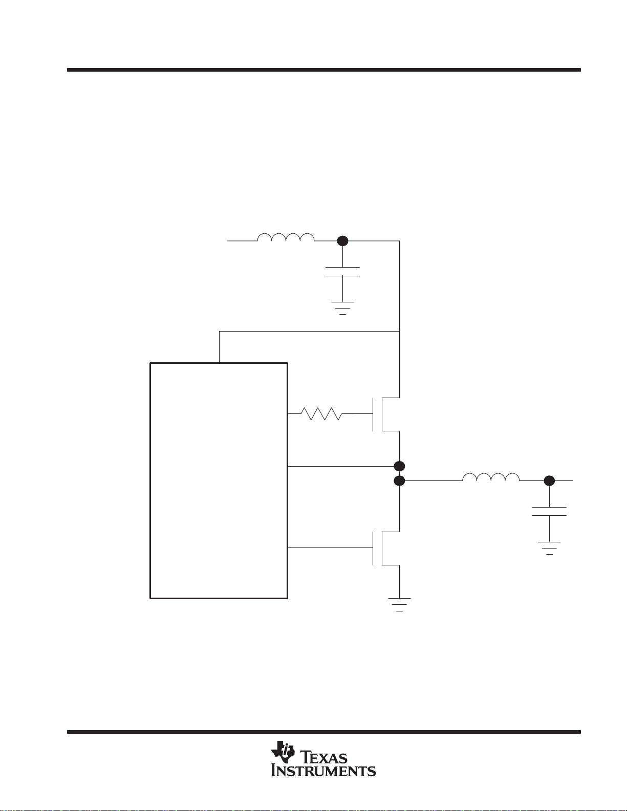
overshoot of output rectangle wave
The drivers in the TPS5103 controller are fast and can produce high transients on VCC or the junction of Q1 and
Q2(shown below). Care must be taken to insure that these transients do not exceed the absolute maximum
rating for the device or associated external component. A low-ESR capacitor connected directly from Q1 drain
to Q2 source can greatly reduce transient pulses on VCC. Also, Q1 turn-on-speed can be reduced by adding
a resistor (5 – 15 Ω) in series with OUT_u. Poor layout of the switching node (V1 in figure) can result in the
requirement for additional snubber circuitry require from V1 to ground.
C1
TPS5103
V
CC
OUT_u
Q1
V1
Q2
POST OFFICE BOX 655303 • DALLAS, TEXAS 75265
19

TPS5103
MULTIPLE MODE SYNCHRONOUS DC/DC CONTROLLER
SLVS240 – SEPTEMBER 1999
APPLICATION INFORMATION
application for general power
The design shown in this data sheet is a reference design for a general power supply application. An evaluation
module (EVM), TPS5103EVM-136 (SLVP136), is available for customer testing and evaluation. The intent is
to allow a customer to fully evaluate the given design using the plug-in EVM supply shown here. For subsequent
customer board revisions, the EVM design can be copied onto the users PCB to shorten design cycle time,
component count, and board cost.
To help the customers to design the power supply using TPS5103, some key design procedures are shown
below.
R2
R6B
R6A
R7
JP1 JP2
C8
C9
R10
C4
C15
C5
R4
R5
C7
C6
R9
R3
TP1
TP2
TP3
TP4
TP5
TP6
TP7
TP8
TP9
TP10
TP18
TP17
TP16
TP15
TP14
TP13
TP12
TP11
D2
R13
C12
C10
C13
R11
R12
C11
TP26
J13
J14
Q2
Q1
C14
C1
+
C2
L1
+
D1
C3
J1
J2
J3
J4
J5
R1
J6
J7
J8
J9
J10
J11
J12
Vi
Vi
Input GND
Input GND
Input GND
SENSE
Vo
Vo
Vo
VoGND
VoGND
VoGND
Figure 36. EVM Schematic
20
POST OFFICE BOX 655303 • DALLAS, TEXAS 75265

MULTIPLE MODE SYNCHRONOUS DC/DC CONTROLLER
SLVS240 – SEPTEMBER 1999
APPLICATION INFORMATION
output voltage setpoint calculation
The output voltage is set by the reference voltage and the voltage divider. In TPS5102, the reference voltage
is 1.185 V , and the divider is composed of two resistors in the EVM design that are R4 and R5, or R14 and R15.
The equation for the setpoint is:
R1 Vr
R2
+
Vo*Vr
Where R1 is the top resistor (kΩ) like R4 or R15; R2 is the bottom resistor (kΩ) such as R5 or R14; Vo is the
required output voltage (V); Vr is the reference voltage (1.185 V in TPS5103).
Example: R1 = 1 kΩ; Vr = 1.185 V; Vo = 1.8 V, then R2 = 1.9 kΩ.
For your convenience, some of the most popular output voltage setpoints are calculated in the table below:
Vo 1.3 V 1.5 V 1.8 V 2.5 V 3.3 V 5.0 V
R1 (top) (kΩ) 1 1 1 1 1 1
R2 (bottom) (kΩ) 10 3.7 1.9 0.9 0.56 0.31
If higher precision resistor is used, the output voltage setpoint can be more accurate.
TPS5103
In some applications, the output voltage is required to be lower than the reference voltage. With few extra
components, the lower voltage can be easily achieved. The drawing below shows the method.
R
Zener
z1
V
CC
V
O
R
(top)
R
(bottom)
INV
TPS5103
R
z2
In the schematic, the Rz1, Rz1, and the zener are the extra components. Rz1 is used to give zener enough
current to build up the zener voltage. The zener voltage is added to INV through Rz2. Therefore, the voltage
on INV is still equal to the IC internal voltage (1.185 V) even if the output voltage is regulated at lower setpoint.
The equation for setting up the output voltage is shown below:
Rz2
+
ǒ
Vr–Vo
Rtop
(
Vz–Vr
Ǔ
)
)
Vr
Rbtm
Where Rz2 is the adjusting resistor for low output voltage; Vz is the zener voltage; Vr is the internal reference
voltage; Rtop is the top resistor of voltage sensing network; Rbtm is the bottom resistor of the sensing network;
Vo is the required output voltage setpoint.
Example: Assuming the required output voltage setpoint is Vo = 0.8 V, Vz = 5 V; Rtop = 1 kΩ; Rbottom = 1 kΩ,
then the Rz2 = 2.43 kΩ.
POST OFFICE BOX 655303 • DALLAS, TEXAS 75265
21

TPS5103
MULTIPLE MODE SYNCHRONOUS DC/DC CONTROLLER
SLVS240 – SEPTEMBER 1999
APPLICATION INFORMATION
switching frequency
With hysteretic control, the switching frequency is a function of the input voltage, the output voltage, the
hysteresis window, the delay of the hysteresis comparator and the driver , the output inductance, the resistance
in the output inductor, the output capacitance, the ESR and ESL in the output capacitor , the output current, and
the turnon resistance of high side and low side MOSFET . It is a very complex equation if everything is included.
To make it more useful to the designers, a simplified equation only considers the most influential factors. The
tolerance of this equation is about 30%:
*
7
)
Td)ńC
*
out
)
out
ESL Vin)
ƒs
+
Vin
V
out
(Vin
(V
*
V
in
out
ESR (10 10
) (ESR*(10 10
*
7
)
Td))0.0097 L
Where fs is the switching frequency (Hz);
output capacitance;
series inductance in the output capacitor (H);
time constant (S).
In the EVM module design, for the 1.8 V output, for example: Vin = 5 V, Vout = 1.8 V, Cout = 680 µF; ESR =
40 mΩ; ESL = 3 nH; Lout = 6 µH; Td = 0.5 µs.
Then, the frequency
ESR
is the equivalent series resistance in the output capacitor (Ω);
fs = 122 kHz.
Vout
is the output voltage (V);
Lout
is the output inductance (H);
Vin
is the input voltage (V);
ESL
Td
is output feedback RC filter
is the equivalent
output inductor ripple current
The output inductor current ripple can affect not only the efficiency and the inductor saturation, but also the
output voltage capacitor selection. The equation is exhibited as below:
Iripple
Where
the
cycle; and Ts is the switching cycle (S). From the equation, it can be seen that the current ripple can be adjusted
by changing the output inductor value.
Example: Vin = 5 V; Vout = 1.8 V; Iout = 5 A; Rdson = 10 mΩ; RL = 5 mΩ; D = 0.36; Ts = 10 µS; Lout = 6 µH
Then, the ripple Iripple = 2 A.
Iripple
output voltage (V);
Vin*Vout*Iout
+
is the peak-to-peak ripple current (A) through inductor;
Iout
is the output current;
Lout
(
Rdson)RL
)
D
Rdson
Ts
Vin
is the input voltage (V);
is the on-time resistance of MOSFET (Ω); D is the duty
Cout
is the
Vout
is
output capacitor RMS current
Assuming the inductor ripple current totally goes through the output capacitor to the ground, the RMS current
in the output capacitor can be calculated as:
D
Io(rms)
Where
current (A).
Example: ∆I = 2 A, so Io(rms) = 0.58 A
22
I(orms)
I
+
Ǹ
12
is the maximum RMS current in the output capacitor (A); ∆I is the peak-to-peak inductor ripple
POST OFFICE BOX 655303 • DALLAS, TEXAS 75265

MULTIPLE MODE SYNCHRONOUS DC/DC CONTROLLER
SLVS240 – SEPTEMBER 1999
APPLICATION INFORMATION
input capacitor RMS current
Assuming the input ripple current totally goes into the input capacitor to the power ground, the RMS current in
the input capacitor can be calculated as:
TPS5103
2
Ii(rms)
Where
From the equation, it can be seen that the highest input RMS current usually occurs at the lowest input voltage,
so it is the worst case design for input capacitor ripple current.
Ii(rms)
Ǹ
+
I
D (1*D))
o
is the input RMS current in the input capacitor (A); Io is the output current (A); D is the duty cycle.
1
12
D
Iripple
2
Example: Io = 5 A; D = 0.36
Then, Ii(rms)= 3.36 A
softstart
The softstart timing can be adjusted by selecting the soft-start capacitor value. The equation is
C
+2
soft
Where
Example: Tsoft = 5 mS, so Csoft = 0.01 µF.
C
soft
T
soft
is the softstart capacitance (µF); T
is the start-up time on softstart terminal (S).
soft
current protection
The current protection in TPS5103 is set using an internal current source and an external resistor to set up the
current limit. The sensed high side MOSFET drain-to-source voltage drop is compared to the set point, if the
voltage drop exceeds the limit, the internal oscillator is activated, and it continuously resets the current limit until
the over-current condition is removed. The equation below should be used for calculating the external resistor
value for current protection:
Rds(on) (Itrip)Iind(p-p)ń2)
Rcl
PWM or HYS mode
SKIP mode
Where Rcl is the external current limit resistor (R10,R1 1); Rds(on) is the high side MOSFET on-time resistance.
Itrip is the required current limit; Iind(p-p) is the peak-to-peak output inductor current.
Example: PWM mode or HYS mode
Rds(on) = 10 mΩ, Itrip =5 A, Iind = 2 A, so Rcl = 4 kΩ
Example: SKIP mode
Rds(on) = 10 mΩ, Itrip = 2 A, Iind = 1 A, so Rcl = 5 kΩ
+
Rds(on) (Itrip)Iind(p-p)ń2)
Rcl
+
0.000015
0.000005
POST OFFICE BOX 655303 • DALLAS, TEXAS 75265
23
TPS5103
MULTIPLE MODE SYNCHRONOUS DC/DC CONTROLLER
SLVS240 – SEPTEMBER 1999
APPLICATION INFORMATION
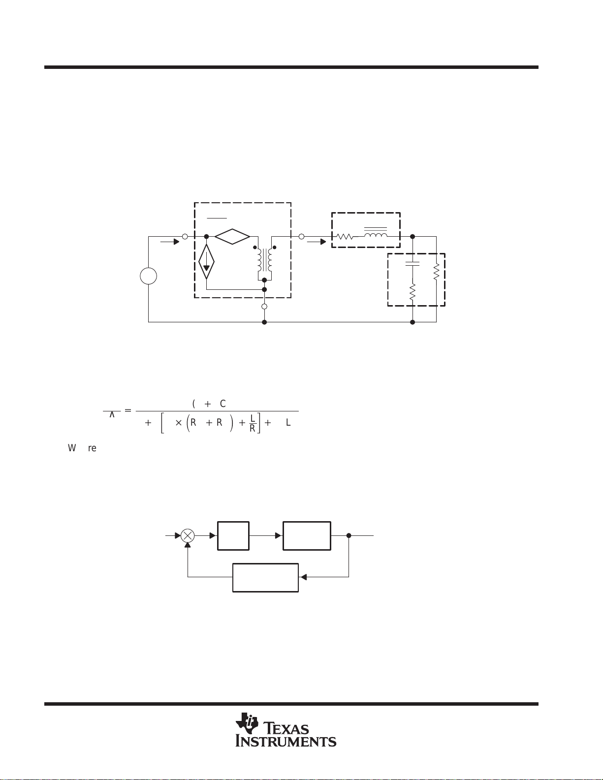
loop gain compensation
Voltage mode control is used in this controller for the output voltage regulation. To achieve fast, stabilized
control, two parts are discussed in this section: the power stage small signal modeling and the compensation
circuit design.
For the buck converter, the small signal modeling circuit is shown below:
Z
∧
V
ap
d
ac
i
a
+
V
I
D
Ic d
+
–
i
1
∧
D
p
c
L
R
L
L
C
Z
RC
R
C
V
O
R
From this equivalent circuit, several control transfer functions can be derived: input-to-output, output
impedance, and control-to-output. Typically the control-to-output transfer function is used for the feedback
control design.
Assuming Rc and RL are much smaller than R, the simplified small signal control-to-output transfer function is:
∧
Vod
∧
d
+
1)sƪC
(
1)sCRc
ǒRc)R
)
L
Ǔ
ƫ
)
)
L
s2LC
R
Where C is the output capacitance; Rc is the equivalent serial resistance (ESR) in the output capacitor; L is the
output inductor; RL is the equivalent serial resistance (ESR) in the output inductor; R is the load resistance.
T o achieve the fast transient response and the better output voltage regulation, a compensation circuit is added
to improve the feedback control. The whole system is shown below:
V
ref
PWM
Compensation
Power
Stage
24
POST OFFICE BOX 655303 • DALLAS, TEXAS 75265

MULTIPLE MODE SYNCHRONOUS DC/DC CONTROLLER
SLVS240 – SEPTEMBER 1999
APPLICATION INFORMATION
The typical compensation circuit used as an option in the EVM design is a part of the output feedback circuit.
The circuitry is displayed below.
TPS5103
C3
R4
C2
_
+
C1
R3
R2R1
V
ref
This circuit is composed of one integrator, two poles, and two zeros:
Assuming R1 << R2 and C2 << C3, the equation is:
Comp
(
1)sC3R4) (1)sC2R2
+
sC3R2(1)sC2R4)(1)sC1R1
)
)
Therefore,
Pole1
+
Zero2
+
Integrator
1
2pC1R1
1
2pC3R4
+
2pƒC3R2
Pole2
Zero1
1
+
2pC2R4
+
2pC2R2
1
1
To PWM
A simplified version used in the EVM design is exhibited below.
Vo
R2
R3
V
ref
C3
R4
C2
_
+
Assuming C2 << C3, the equation is:
Comp
(
+
1)sC3R4
sC3R2(1)sC2R4
)
)
POST OFFICE BOX 655303 • DALLAS, TEXAS 75265
25

TPS5103
MULTIPLE MODE SYNCHRONOUS DC/DC CONTROLLER
SLVS240 – SEPTEMBER 1999
APPLICATION INFORMATION
there is one pole, one zero and one integrator:
Zero
+
2pC3R4
1
Pole
+
2pC2R4
1
Integrator
+
1
2pƒC3R2
The loop-gain concept is used to design a stable and fast feedback control. The loop-gain equation is derived
by that the control-to-output transfer function times the compensation:
Loop*gain+Vod X Comp
By using a bode plot, the amplitude and the phase of this equation can be drawn with software such as MathCad.
In turn, the stability can be easily designed by adjusting the compensation perimeters. The sample bode plot
is shown below to explain the phase margin, gain margin and the crossover frequency.
The gain is drawn as 20 log (loop-gain), and the phase is in degrees. To explain them clearer, 180 degrees is
added to the phase, so that the gain and phase share the same zero.
Where the gain curve touches the zero is the crossover frequency . The higher this frequency is, the faster the
transient response is, since the transient recovery time is 1/(crossover frequency). The phase to the zero is the
phase margin at the crossover frequency. The phase margin should be at least 60 degrees to cover all the
condition changes such as temperature. The gain margin is the gap between gain curve and the zero when the
phase curve touches the zero. This margin should be at least 20 dB to guarantee the stability over all conditions.
180
166
20 Log (Loop-Gain)
180 + Phase
152
138
124
110
96
82
68
54
40
26
12
–2
–16
–30
–44
–58
–72
–86
–100
Gain
10 100 10
Phase
Margin
Phase
Crossover
f – Frequency – Hz
Gain
Margin
3
10
4
10
5
10
6
26
POST OFFICE BOX 655303 • DALLAS, TEXAS 75265

MULTIPLE MODE SYNCHRONOUS DC/DC CONTROLLER
SLVS240 – SEPTEMBER 1999
APPLICATION INFORMATION
synchronization
Some applications require switching clock synchronization. Two methods are used for synchronization:
D
Triangle wave synchronization
TPS5103
D
Square wave synchronization
740 mV
740 mV
C
R
t
t
TPS5103
It can be seen that RT and CT are removed from the circuit. Therefore, two components are saved. This method
is good for the synchronization between two controllers. If the controller needs to be synchronized with digital
circuit such as DSP, usually the square-type clock signal is used. The configuration exhibited below is for this
type of application:
C
t
TPS5103
R
t
An external resistor is added into the circuit, but R
is still removed. C
T
is kept to be a part of RC circuit generating
T
triangle waveform for the controller. Assuming the peak value of the square is known, the resistor and the
capacitor can be adjusted to achieve the correct peak–to–peak value and the offset value.
layout guidelines
Good power supply results will only occur when care is given to proper design and layout. Layout will affect noise
pickup and generation and can cause a good design to perform with less than expected results. With a range
of currents from milliamps to tens or even hundreds of amps, good power supply layout is much more difficult
than most general PCB designs. The general design should proceed from the switching node to the output, then
back to the driver section and, finally, place the low-level components. Below are several specific points to
consider before layout of a TPS5103 design begins.
D
All sensitive analog components should be referenced to ANAGND. These include components connected
to Vref5, Vref, INV, LH, and COMP .
D
Analog ground and drive ground should be isolated as much as possible. Ideally , analog ground will connect
to the ground side of the bulk storage capacitors on VO, and drive ground will connect to the main ground
plane close to the source of the low-side FET.
POST OFFICE BOX 655303 • DALLAS, TEXAS 75265
27

TPS5103
MULTIPLE MODE SYNCHRONOUS DC/DC CONTROLLER
SLVS240 – SEPTEMBER 1999
APPLICATION INFORMATION
D
Connections from the drivers to the gate of the power FETs should be as short and wide as possible to
reduce stray inductance. This becomes more critical if external gate resistors are not being used.
D
The bypass capacitor for VCC should be placed close to the TPS5103.
D
When configuring the high-side driver as a floating driver, the connection from LL to the power FETs should
be as short and as wide as possible.
D
When configuring the high-side driver as a floating driver, the bootstrap capacitor (connected from LH to
LL) should be placed close to the TPS5103.
D
When configuring the high-side driver as a ground-referenced driver, LL should be connected to DR VGND.
D
The bulk storage capacitors across VIN should be placed close to the power FETS. High-frequency bypass
capacitors should be placed in parallel with the bulk capacitors and connected close to the drain of the
high-side FET and to the source of the low-side FET.
D
High-frequency bypass capacitors should be placed across the bulk storage capacitors on VO.
D
LH and LL should be connected very close to the drain and source, respectively , of the high-side FET. LH
and LL should be routed very close to each other to minimize differential-mode noise coupling to these
traces. Ceramic decoupling capacitors should be placed close to where VCC connects to Vin, to reduce
high-frequency noise coupling on V
D
The output voltage sensing trace should be isolated by either ground trace or VCC trace.
CC
.
test results
The tests are conducted at TA = 25°C, the point voltage is 5 V.
28
POST OFFICE BOX 655303 • DALLAS, TEXAS 75265

TPS5103
MULTIPLE MODE SYNCHRONOUS DC/DC CONTROLLER
SLVS240 – SEPTEMBER 1999
APPLICATION INFORMATION
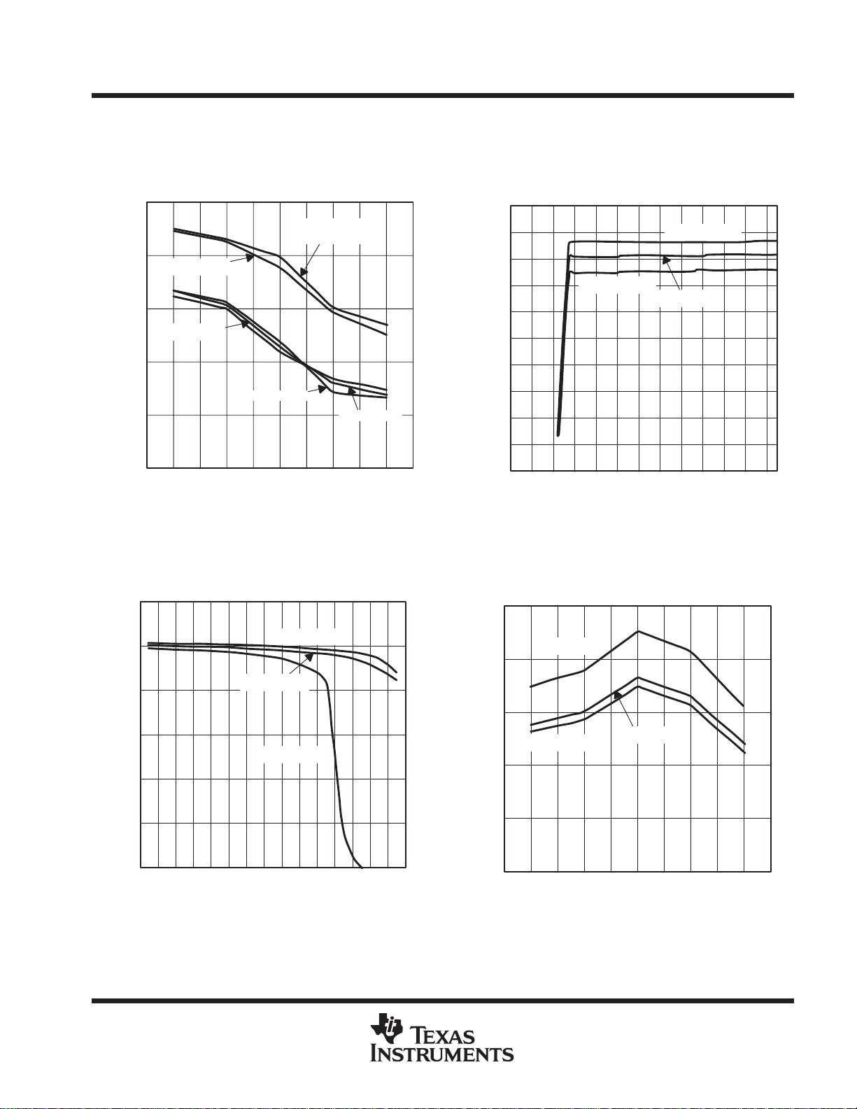
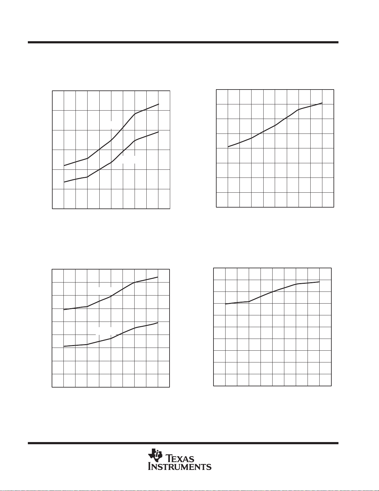
EFFICIENCY
OUTPUT CURRENT
95
1.8 V Output Efficiency
90
85
80
75
Efficiency – %
70
65
60
0 0.5 1 1.5 2 2.5 3
PWM Mode
SKIP Mode
IO – Output Current – A
Figure 37
OUTPUT VOLTAGE
INPUT VOLTAGE
1.790
1.8 V Line Regulation
vs
vs
3.5 4
95
1.8 V Output Efficiency
90
85
80
75
Efficiency – %
70
65
60
0 0.1 0.2 0.3
IO – Output Current – A
1.790
1.8 V Output Load Regulation
EFFICIENCY
vs
OUTPUT CURRENT
PWM Mode
SKIP Mode
0.4 0.5
Figure 38
OUTPUT VOLTAGE
vs
OUTPUT CURRENT
1.785
1.780
– Output Voltage – V
O
V
1.775
1.770
51015
VI – Input Voltage – V
Figure 39
1.790
1.780
1.780
– Output Voltage – VV
1.770
O
1.770
20 250
1.760
0 0.5 1 1.5 2 2.5 3
IO – Output Current – A
3.5 4
Figure 40
POST OFFICE BOX 655303 • DALLAS, TEXAS 75265
29

TPS5103
MULTIPLE MODE SYNCHRONOUS DC/DC CONTROLLER
SLVS240 – SEPTEMBER 1999
EFFICIENCY
OUTPUT CURRENT
95
1.8 V Output Diode Type Efficiency
90
85
80
75
Efficiency – %
70
65
60
0 0.5 1 1.5 2 2.5 3
IO – Output Current – A
Figure 41
TRANSIENT RESPONSE (OVERSHOOT)
vs
OUTPUT/VOLTAGE
OUTPUT VOLTAGE
3.5 4
Figure 42
TRANSIENT RESPONSE (UNDERSHOOT)
30
Figure 43
Figure 44
POST OFFICE BOX 655303 • DALLAS, TEXAS 75265

TPS5103
MULTIPLE MODE SYNCHRONOUS DC/DC CONTROLLER
SLVS240 – SEPTEMBER 1999
APPLICATION INFORMATION
Table 1. Bill of Materials (see Note 3)
REF PN DESCRIPTION MFG SIZE
C1opt 10TPB220M Capacitor, POSCAP, 220 µF, 10 V Sanyo 7.3x4.3mm
C1 RV-35V221MH10-R Capacitor, electrolytic, 220 µF, 35 V ELNA 10x10mm
C2 GMK325F106ZH Capacitor, ceramic, 10 µF, 35 V T aiyo Yuden 1210
C3 4TPB470M Capacitor, POSCAP, 470 µF, 4 V Sanyo 7.3x4.3mm
†
C4
C5 std Capacitor, ceramic, 1 µF, 16 V 805
C6 std Capacitor, ceramic, 0.01 µF, 16 V 805
C7 std Capacitor, ceramic, 220 pF, 16 V 805
C8 std Capacitor, ceramic, 100 pF, 16 V 805
C9 std Capacitor, ceramic, 1 µF, 16 V 805
C10 GMK316F225ZG Capacitor, ceramic, 2.2 µF, 35 V Taiyo Yuden 1206
†
C11
C12 GMK316F225ZG Capacitor, Ceramic, 2.2 µF, 35 V Taiyo Yuden 1206
C13 GMK325F106ZH Capacitor, Ceramic, 10 µF, 35 V Taiyo Yuden 1210
C14 Open
C14†opt Open 10x10mm
†
C15
D1 MBRS340T3 Diode, Schottky, 40 V, 3 A Motorola SMC
D1opt MBRS130LT3 Diode, Schottky, 30 V, 1 A Motorola SMB
D2 SD103-AWDICT-ND Diode, Schottky, 40 V, 200 mA, 400 mW Digikey 3.5x1.5mm
L1 DO3316P-682 Inductor, 6.8 uH, 4.4 A Coilcraft 0.5x0.37 in
J1–J14 CA26DA-D36W-0FC Edge connector, surface-mount, 0.040” board, 0.090” standoff NAS Interplex 0.040”
JP1 S1132-2-ND Header, straight, 2–pin, 0.1 ctrs, 0.3” pins Sullins DigiKey #
JP1 Shunt 929950-00-ND Shunt, jumper, 0.1” 3M DigiKey
JP2 S1132-2-ND Header, straight, 2–pin, 0.1 ctrs, 0.3” pins Sullins DigiKey
R1 std Resistor, 5.1 kΩ, 5 % 805
†
R2
R3 std Resistor, 910 Ω, 1% 805
R4 std Resistor, 1.74 kΩ, 1% 805
R5 std Resistor, 5.1 kΩ, 5% 805
R6A std Resistor, 82 kΩ, 5% 805
†
R6B
R7 std Resistor, 1 kΩ, 5% 805
R9 std Resistor, 1 kΩ, 5% 805
R10 std Resistor, 1 kΩ, 5% 805
R11 std Resistor, 10 Ω, 5% 805
R12 std Resistor, 51 kΩ, 5% 805
†
R13
Q1 Si4410DY Transistor, MOSFET, n-ch, 30-V, 10-A, 13–mΩ Siliconix SO–8
Q2 Si4410DY Transistor, MOSFET, n-ch, 30-V, 10-A, 13-mΩ Siliconix SO–8
U1 TPS5103 IC, controller TI SSOP–20
†
Components for optional mode test only.
NOTE 3: This operation mode is PWM mode only.
std Open, capacitor, Ceramic, 2.2 µF, 16 V 805
std Open 805
std Open, capacitor, ceramic, 1000 pF, 16 V 805
S1132-2-ND
#929950-00-ND
#S1132-2-ND
std Open, resistor, 1 kΩ, 5% 805
std Open, 0 Ω, 5% 805
std Open 805
POST OFFICE BOX 655303 • DALLAS, TEXAS 75265
31

TPS5103
MULTIPLE MODE SYNCHRONOUS DC/DC CONTROLLER
SLVS240 – SEPTEMBER 1999
APPLICATION INFORMATION
Top Layer
.
Bottom Layer (Top View)
32
POST OFFICE BOX 655303 • DALLAS, TEXAS 75265

TPS5103
MULTIPLE MODE SYNCHRONOUS DC/DC CONTROLLER
SLVS240 – SEPTEMBER 1999
APPLICATION INFORMATION
Top Assembly
NOTE: All wire pairs should be twisted.
–
Load
0 – 4 A
POST OFFICE BOX 655303 • DALLAS, TEXAS 75265
+
Test Setup
Power Supply
5–V, 5–A Supply
–
+
33

TPS5103
MOSFETS (Q1–Q2)
Local distributor
INPUT CAPACITORS (C1)
MULTIPLE MODE SYNCHRONOUS DC/DC CONTROLLER
SLVS240 – SEPTEMBER 1999
APPLICATION INFORMATION
Table 2. Test Specifications
PARAMETER CONDITIONS MIN TYP MAX UNITS
Input voltage range 5 25 V
Output voltage range Vi = 5 – 25 V Io = 0 – 4 A 1.7 1.8 1.9 V
Output current range Vi = 5 – 10 V 0 4 A
Output current limit Vi = 5 V 4.3 A
Output ripple Vi =5 V, Io = 4 A 50 mVp–p
Operating frequency Io = 4 A 150 250 KHz
Efficiency Vi = 5 V, Vo = 1.8 V, Io = 4 A 90 %
Table 3. EVM Operating Specifications
SKIP MODE HYS MODE
Remove JP1 shunt Remove R5, C6 and C7
Remove R6A
Add R6B
Add C15
If it needs the loop-compensation, add R2 and C4
This EVM is designed to cover as many applications as possible. For some more specific applications, the circuit
can be simpler. The table below gives some recommendations.
Table 4. EVM Application Recommendations
5-V INPUT VOLTAGE <3-A OUTPUT CURRENT DIODE VERSION
Change C1 to low profile capacitor
Sanyo 10TPB220M (220 µF, 10 V)
Or 6TPB330M (330 µF, 6.3 V)
Remove R10
Change Q1 and Q2 to dual pack MOSFET,
IRF7311 to reduce the cost.
Remove Q2 to reduce the cost.
Table 5. Vendor and Source Information
MATERIAL SOURCE PART NUMBER DISTRIBUTORS
In EVM design Si4410
Second source IRF7811 (International Rectifier)
In EVM design RV–35V221MH10–R (ELNA) Bell Microproducts 972–783–4191
Second source 35CV330AX/GX (Sanyo) 870–633–5030
UUR1V221MNR1GS (Nichicon) Future Electronics (Local Office)
MAIN DIODES (D1) In EVM design MBRS340T3 (Motorola) Local distributors
Second source U3FWJ44N (Toshiba) Local distributors
INDUCTORS (L1) In EVM design DO3316P–682 (Coilcraft) 972–458–2645
CTDO3316P–682
(Inductor Warehouse)
GMK325F106ZH
GMK316F225ZG
(Taiyo Yuden)
800–533–8295
SMEC
512–331–1877
CERAMIC CAPACITORS
(C2, C14) (C12, C10)
Second source
IN EVM design
Taiyo Yuden representative e–mail: mike@millsales.com
34
POST OFFICE BOX 655303 • DALLAS, TEXAS 75265

MULTIPLE MODE SYNCHRONOUS DC/DC CONTROLLER
SLVS240 – SEPTEMBER 1999
APPLICATION INFORMATION
High current applications are described in Table 6. The values are recommendations based on actual test
circuits. Many variations are possible based on the requirements of the user. Performance of the circuit is
dependent upon the layout rather than on the specific components, if the device parameters are not exceeded.
The power stage, having the highest current levels and greatest dv/dt rates, should be given the most attention,
as both the supply and load can be severely affected by the power levels and edge rates.
Table 6. High Current Applications
TPS5103
REFERENCE
DESIGNATIONS
C1 Input bulk capacitor
C2 Input bypass capacitor
L1 Output filter indicator
C3 Output filter capacitor
Q1 Power switch
Q2 Power switch
R11 Gate drive resistor 7 Ω 5 Ω 4 Ω
R12 Current limit resistor 10 kΩ 15 kΩ 20 kΩ
Switching frequency 200 kHz 150 kHz 100 kHz
FUNCTION 8-A OUTPUT 12-A OUTPUT 16-A OUTPUT
2x ELNA
RV-35V221MH10-R
220 µF, 35 V
2x Taiyo Yuden
GMK325F106ZH
10 µF, 35 V
Coiltronics UP3B-2R2
2.2 µΗ, 9.2 A
2x Sanyo 4TPB470M
470 µF, 4 V
2x Siliconix Si4410DY
30 V, 10 A, 13 mΩ
2x Siliconix Si4410DY
30 V, 10 A, 13 mΩ
3x ELNA
RV-35V221MH10-R
220 µF, 35 V
3x Taiyo Yuden
GMK325F106ZH
10 µF, 35 V
Coiltronics UP4B-1R5
1.5 µΗ, 13.4 A
3x Sanyo 4TPB470M
470 µF, 4 V
3x Siliconix Si4410DY
30 V, 10 A, 13 mΩ
3x Siliconix Si4410DY
30 V, 10 A, 13 mΩ
4x ELNA
RV-35V221MH10-R
220 µF, 35 V
4x Taiyo Yuden
GMK325F106ZH
10 µF, 35 V
MicorMetals T68-8/90
Core w/7T, #16
1.0 µΗ, 25 A
4x Sanyo 4TPB470M
470 µF, 4 V
4x Siliconix Si4410DY
30 V, 10 A, 13 mΩ
4x Siliconix Si4410DY
30 V, 10 A, 13 mΩ
POST OFFICE BOX 655303 • DALLAS, TEXAS 75265
35

TPS5103
MULTIPLE MODE SYNCHRONOUS DC/DC CONTROLLER
SLVS240 – SEPTEMBER 1999
MECHANICAL DATA
DB (R-PDSO-G**) PLASTIC SMALL-OUTLINE PACKAGE
28 PINS SHOWN
0,65
28
1
2,00 MAX
0,38
0,22
15
14
A
0,05 MIN
0,15
5,60
5,00
M
8,20
7,40
Seating Plane
0,10
0,15 NOM
Gage Plane
0°–8°
0,25
1,03
0,63
PINS **
DIM
A MAX
A MIN
NOTES: A. All linear dimensions are in millimeters.
B. This drawing is subject to change without notice.
C. Body dimensions do not include mold flash or protrusion not to exceed 0,15.
D. Falls within JEDEC MO-150
8
3,30
2,70
14
6,50
6,50
5,905,90
2016
7,50
6,90
24
8,50
28
10,50
9,907,90
30
10,50
9,90
38
12,90
12,30
4040065 /C 10/95
36
POST OFFICE BOX 655303 • DALLAS, TEXAS 75265

IMPORTANT NOTICE
T exas Instruments and its subsidiaries (TI) reserve the right to make changes to their products or to discontinue
any product or service without notice, and advise customers to obtain the latest version of relevant information
to verify, before placing orders, that information being relied on is current and complete. All products are sold
subject to the terms and conditions of sale supplied at the time of order acknowledgement, including those
pertaining to warranty, patent infringement, and limitation of liability.
TI warrants performance of its semiconductor products to the specifications applicable at the time of sale in
accordance with TI’s standard warranty. Testing and other quality control techniques are utilized to the extent
TI deems necessary to support this warranty . Specific testing of all parameters of each device is not necessarily
performed, except those mandated by government requirements.
CERTAIN APPLICATIONS USING SEMICONDUCTOR PRODUCTS MAY INVOLVE POTENTIAL RISKS OF
DEATH, PERSONAL INJURY, OR SEVERE PROPERTY OR ENVIRONMENTAL DAMAGE (“CRITICAL
APPLICATIONS”). TI SEMICONDUCTOR PRODUCTS ARE NOT DESIGNED, AUTHORIZED, OR
WARRANTED TO BE SUITABLE FOR USE IN LIFE-SUPPORT DEVICES OR SYSTEMS OR OTHER
CRITICAL APPLICA TIONS. INCLUSION OF TI PRODUCTS IN SUCH APPLICATIONS IS UNDERST OOD TO
BE FULLY AT THE CUSTOMER’S RISK.
In order to minimize risks associated with the customer’s applications, adequate design and operating
safeguards must be provided by the customer to minimize inherent or procedural hazards.
TI assumes no liability for applications assistance or customer product design. TI does not warrant or represent
that any license, either express or implied, is granted under any patent right, copyright, mask work right, or other
intellectual property right of TI covering or relating to any combination, machine, or process in which such
semiconductor products or services might be or are used. TI’s publication of information regarding any third
party’s products or services does not constitute TI’s approval, warranty or endorsement thereof.
Copyright 1999, Texas Instruments Incorporated
 Loading...