

SLUS564C − JULY 2003 − REVISED OCTOBER 2008
FEATURES
Wide Input Voltage Range: 4.5-V to 28-V
D
D Selectable Dual and DDR Modes
D Selectable Fixed Frequency Voltage Mode
D Advanced Power Good Logic Monitors both
Channels
D Selectable Autoskip Mode
D Integrated Boot Strap Diodes
D 180° Phase Shift Between Channels
D Integrated 5-V, 60-mA Regulator
D Input Feedforward Control
D 1% Internal 0.85-V Reference
D R
Overcurrent Detection (4200 ppm/°C)
DS(on)
D Integrated OVP, UVP and Power Good Timers
D 30-pin TSSOP Package
APPLICATIONS
Notebook Computers System Bus and I/O
D
D DDR I or DDR II Termination
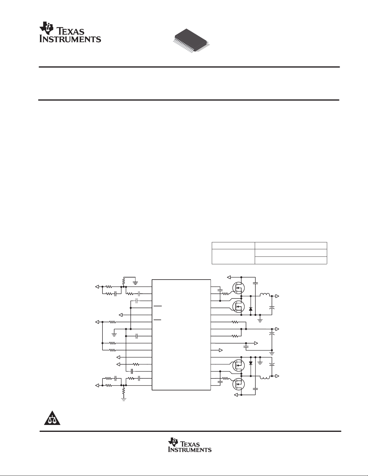
SIMPLIFIED
APPLICATION
DIAGRAM
VO1
VO2
VIN
VO1
VO2
VREG5
1
INV1
2
COMP1
3
SSTRT1
4
SKIP
5
VO1_VDDQ
6
DDR
7
GND
8
REF_X
9
ENBL1
10
ENBL2
11
VO2
12
PGOOD
13
SSTRT2
14
COMP2
15
INV2
TPS51020
DESCRIPTION
The TPS51020 is a multi-function dualsynchronous step-down controller for notebook
system power. The part is specifically designed
for high performance, high efficiency applications
where the loss associated with a current sense
resistor is unacceptable. The TPS51020 utilizes
feed forward voltage mode control to attain high
efficiency without sacrificing line response.
Efficiency at light load conditions can be
maintained high as well by incorporating autoskip
operation. A selectable, Suspend to RAM (STR)
supported, DDR option provides a one chip
solution for all switching applications from
5-V/3.3-V supply to a complete DDR termination
solution.
ORDERING INFORMATION
TA PLASTIC TSSOP (DBT)
VBST1
OUT1_U
LL1
OUT1_D
OUTGND1
TRIP1
VIN
TRIP2
VREG5
REG5_IN
OUTGND2
OUT2_D
LL2
OUT2_U
VBST2
−40°C to 85°C
VIN
30
29
28
27
26
25
24
23
22
21
EXT_5V
20
19
18
17
16
VIN
TPS51020DBTR (T&R)
VREG5
TPS51020DBT
VO1
VIN
VO2
UDG−03144
Please be aware that an important notice concerning availability, standard warranty, and use in critical applications of
Texas Instruments semiconductor products and disclaimers thereto appears at the end of this data sheet.
!"#$%&" ' ()##*& %' "! +),-(%&" .%&*/
#".)(&' ("!"#$ &" '+*(!(%&"' +*# &0* &*#$' "! *1%' '&#)$*&'
'&%.%#. 2%##%&3/ #".)(&" +#"(*''4 ."*' "& *(*''%#-3 (-).*
&*'&4 "! %-- +%#%$*&*#'/
www.ti.com
Copyright 2003, Texas Instruments Incorporated
1
V
Ouput voltage range
V
I/O Voltage
SLUS564C − JULY 2003 − REVISED OCTOBER 2008
ABSOLUTE MAXIMUM RATINGS
Over operating free-air temperature range unless otherwise noted. All voltage values are with respect to the network ground terminal unless
otherwise noted.
Input voltage range
Ouput voltage range
Output current range
Operating free-air temperature range, T
Storage temperature range, T
Junction temperature range, T
Lead temperature 1,6 mm (1/16 inch) from case for 10 seconds 300
(1)
TPS51020 UNIT
VBST1, VBST2 −0.3 to 35
VBST1, VBST2 (wi th respect to LL ) −0.3 to 7
VIN, TRIP1, TRIP2, ENBL1, ENBL2, DDR −0.3 to 30
SKIP, INV1, INV2 −0.3 to 7
OUT1_U, OUT2_U −1 to 35
OUT1_U, OUT2_U (wi th respect to LL ) −0.3 to 7
LL1, LL2 −1 to 30
REF_X −0.3 to 15
PGOOD, VO1_VDDQ, VO2, OUT1_D, OUT2_D, COMP1, COMP2, VREG5,
SSTRT1, SSTRT2
OUTGND1, OUTGND2 −0.3 to 0.3
VREG5 70
REF_X 7
A
stg
J
−0.3 to 7
−40 to 85
−55 to 150
−40 to 125
V
mA
°C
RECOMMENDED OPERATING CONDITIONS
MIN TYP MAX UNIT
Supply voltage, VIN 4.5 28
Supply voltage, VBST1, VBST2 4.5 33
ENBL1, ENBL2, DDR, TRIP1, TRIP2 −0.1 28
OUT1_U, OUT2_U −0.8 33
OUT1_U, OUT2_U (wi th respect to LL ) −0.1 5.5
LL1, LL2 −0.8 28
I/O Voltage
Source current
Operating free-air temperature, T
(1)
Stresses beyond those listed under absolute maximum ratings may cause permanent damage to the device. These are stress ratings only,
and functional operation of the device at these or any other conditions beyond those indicated under ”recommended operating conditions” is
not implied. Exposure to Absolute Maximum Rated conditions for extended periods may affect device reliability
REF_X −0.1 12
SSTRT1, SSTRT2, COMP1, COMP2 −0.1 5.5
SKIP, INV1, INV2 −0.1 5.5
PGOOD VO1_VDDQ, VO2 −0.1 5.5
OUT1_D, OUT2_D, VREG5 −0.1 5.5
VREG5 60
REF_X 5
A
−40 85 °C
DISSIPATION RATING TABLE
PACKAGE
30-pin DBT 874 mW 7.0 mW/°C 454 mW
TA < 25°C
POWER RATING
FACTOR ABOVE TA = 25°C
DERATING
TA = 85°C
POWER RATING
V
mA
2
www.ti.com
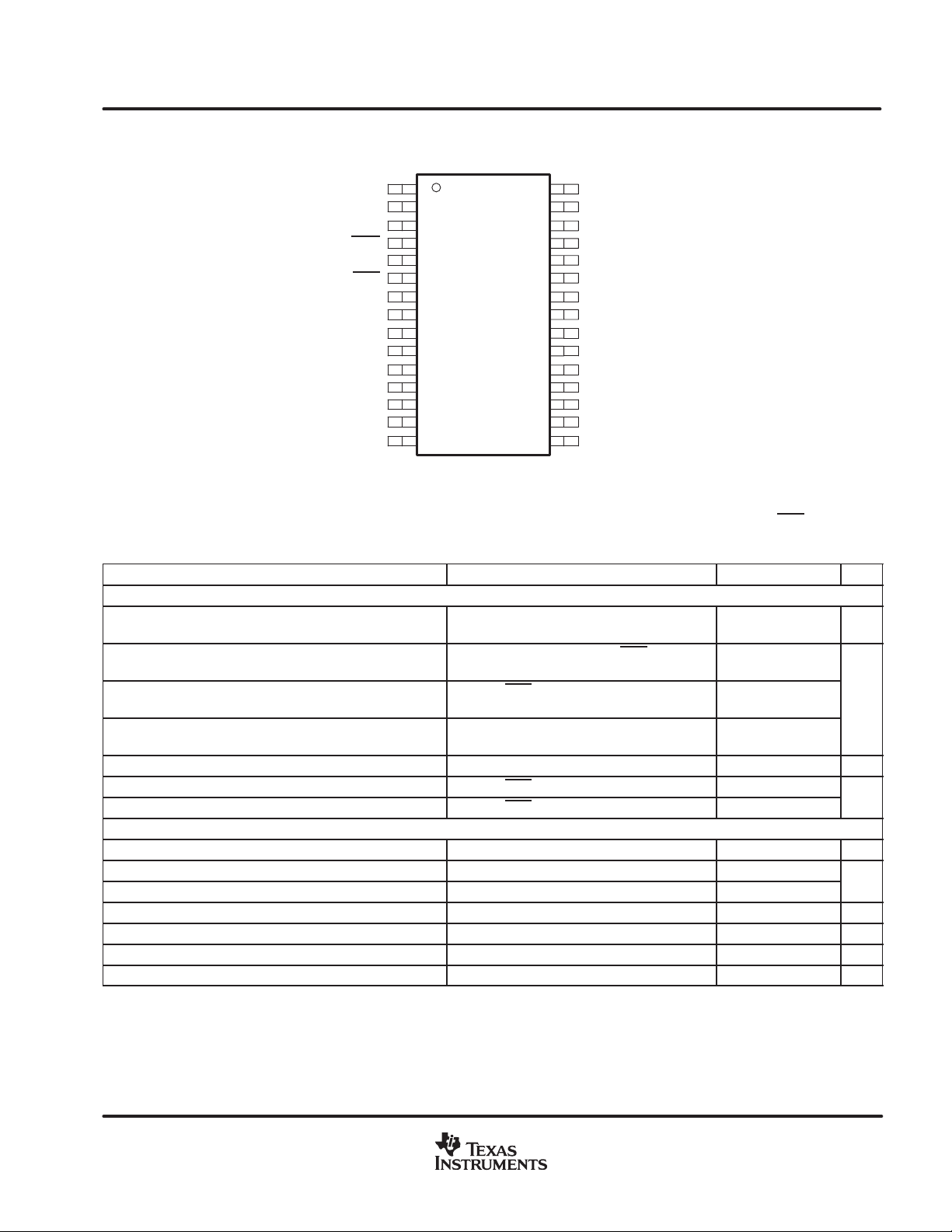
TSSOP (0.5 mm)
DBT PACKAGE
(TOP VIEW)
INV1
COMP1
SSTRT1
SKIP
VO1_VDDQ
DDR
GND
REF_X
ENBL1
ENBL2
VO2
PGOOD
SSTRT2
COMP2
INV2
1
2
3
4
5
6
7
8
9
10
11
12
13
14
15
30
29
28
27
26
25
24
23
22
21
20
19
18
17
16
VBST1
OUT1_U
LL1
OUT1_D
OUTGND1
TRIP1
VIN
TRIP2
VREG5
REG5_IN
OUTGND2
OUT2_D
LL2
OUT2_U
VBST2
ELECTRICAL CHARACTERISTICS
TA = −40°C to 85°C, 4.5 V < VIN < 20 V, C
INVx = COMPx, RSSTRTx = OPEN, TRIP1 = TRIP2 = VIN, LLx = GND, VBSTx = LLx+5, C
OUTGNDx = 0 V , VO1_VDDQ = VO2 = 0 V (unless otherwise stated)
PARAMETER
INPUT CURRENTS
I
VIN
I
VIN(STBY)VIN
I
VIN(SHDN)VIN
I
VIN(REG5)
I
REG5
I
VBSTx
I
VBSTx
VREG5 INTERNAL REGULATOR
V
VREG5
V
LD5
V
LN5
V
THL
V
HYS(UV)
V
TH(SW)
V
HYS(SW)
VIN supply current
standby current
shutdown current
VIN supply current, REG5_IN as 5-V input
current
REG5_IN input supply current REG5V_IN = 5 V, OSC = OFF 1.0 1.7 mA
VBST supply current ENBLx = DDR = VIN 0.05 1.00
VBST shutdown current ENBLx = DDR = 0 V 0.05 1.00
VREG5 voltage I
Load regulation 0 mA ≤ I
Line regulation I
UVLO threshold voltage High to low 3.45 3.65 3.85 V
UVLO hysteresis 100 200 300 mV
Switchover voltage REG_IN voltage 4.2 4.5 4.8 V
Switchover hysteresis 50 250 mV
= 0.1 µF, C
VIN
= 2.2 µF, C
VREG5
REG5V_IN = OPEN, TRIPx = VIN,
OSC = OFF
ENBLx = 0 V, DDR = VIN,
REG5V_IN = OPEN, OSC = OFF
ENBLx = DDR = 0 V,
REG5V_IN = OPEN
REG5V_IN = 5 V, OSC = OFF 200 500
= 0 A 4.8 5.0 5.2 V
OUT
OUT
= 20 mA, 7 V≤VIN ≤ 28 V 0.4% 2.0%
OUT
= 0.01 µF, PGOOD = 0.2 V, ENBLx = DDR = VIN,
REF_X
TEST CONDITIONS MIN TYP MAX UNIT
≤ 50 mA, VIN = 12 V 0.6% 2.5%
SLUS564C − JULY 2003 − REVISED OCTOBER 2008
(OUTx_U, OUTx_D)
=1 nF, REG5_IN = 0V, GND =
1.4 2.2 mA
350 550
0.05 1.00
µA
µA
www.ti.com
3
)
)
SLUS564C − JULY 2003 − REVISED OCTOBER 2008
ELECTRICAL CHARACTERISTICS (continued)
TA = −40°C to 85°C, 4.5 V < VIN < 20 V, C
INVx = COMPx, RSSTRTx = OPEN, TRIP1 = TRIP2 = VIN, LLx = GND, VBSTx = LLx+5, C
OUTGNDx = 0 V , VO1_VDDQ = VO2 = 0 V (unless otherwise stated)
PARAMETER UNITMAXTYPMINTEST CONDITIONS
REF_X REFERENCE VOLTAGE
V
REF10
V
LD10
V
LN10
V
REFVTT
V
REFVTT
POWERGOOD COMPARATORS
V
THDUAL(PG
V
THDDR(PG
T
PG(del)
DIGITAL CONTROL INPUTS
V
IH
V
IL
I
INLEAK
VO1_VDDQ and VO2
R
VOUT
V
VOUTOK
V
VO2LEAK
R
VOUT
UNDERVOLTAGE AND OVERVOLTAGE PROTECTION
V
OVPDUAL
V
OVPDDR
T
OVP(del)
V
UVPDUAL
V
UVPDDR
T
UVP(del)
OVERCURRENT and INPUT VOLTAGE UVLO PROTECTION
I
TRIPSNK
I
TRIPSRC
TC
ITRIP
V
OCPHI
V
OCPLO
V
VINUVLO
V
VINHYS
10-V reference voltage VIN = 14 V, I
Load regulation 0 mA ≤ I
Line regulation I
VTT reference voltage
VTT reference load regulation 0 mA ≤ IO ≤ 3 mA 0.75%
PGOOD threshold (dual mode)
PGOOD threshold (DDR)
PGOOD delay time
High-level input voltage, logic DDR, ENBL1, ENBL2, SKIP 2.2
Low-level input voltage, logic DDR, ENBL1, ENBL2, SKIP 0.3
Logic input leakage current DDR, ENBL1, ENBL2, SKIP= 5 V |1.0| µA
VOx sink impedance V
VOx low restart voltage Fault condition removed, restart 0.25 0.32 0.40 V
VOx input leakage current DDR= VIN, VOx = 5 V |1.0| µA
VO1_VDDQ input impedance DDR= 0 1.5 MΩ
OVP trip output threshold (dual) Sensed at INVx 945 970 1010 mV
OVP trip output threshold (DDR) VO1_VDDQ = 2.5 V 1.31 1.36 1.41 V
OVP propagation delay time
UVP trip output threshold (dual) Sensed at INVx 510 553 595
UVP trip output threshold (DDR) VO1_VDDQ = 2.5 V 750 813 875
UVP propagation delay time 4096 clks
TRIPx sink current V
TRIPx source current V
TRIP current temperature coeficient
High-level OCP comparator offset voltage
Low-level OCP comparator offset voltage
VIN UVLO trip threshold REF5V_IN = 4.8 V 3.7 3.9 4.1 V
VIN UVLO trip hysteresis 100 200 300 mV
= 0.1 µF, C
VIN
(1)
(1)
= 2.2 µF, C
VREG5
OUT
= 100 µA, 14 V≤VIN ≤28 V 5%
OUT
DDR = 0 V wrt VO1_VDDQ input divided by 2
V
= 2.5 V
VO1
Undervoltage PGOOD 765 786 808
Overvoltage PGOOD
Undervoltage PGOOD,
VO1_VDDQ = 2.5 V
Overvoltage PGOOD,
VO1_VDDQ = 2.5 V
INVx > undervoltage PGOOD,
Delay time from SSTRTx > 1.5 V to PGOOD
going high
= 0.5 V, fault engaged 6 10 Ω
VOUTx
= VIN − 100 mV, TA = 25°C 11 13 15
TRIPx
= 100 mV, TA = 25°C 10 13 16
TRIPx
TA = 25°C 4200
(1)
(1)
= 0.01 µF, PGOOD = 0.2 V, ENBLx = DDR = VIN,
REF_X
≤ 2 mA, VIN = 18 V -12% -20%
(OUTx_U, OUTx_D)
= 0 A 8.5 10.0 11.0 V
OUT
=1 nF, REG5_IN = 0V, GND =
1.5%
892 920 945
1.12 1.14 1.16
1.28 1.31 1.33
2048 clks
20 µs
0 |3.0|
0 |5.0|
mV
V
V
mV
µA
ppm/
°C
mV
4
www.ti.com
mV
MAX
DC
MAX
Maximum duty cycle
kHz
SLUS564C − JULY 2003 − REVISED OCTOBER 2008
ELECTRICAL CHARACTERISTICS (continued)
TA = −40°C to 85°C, 4.5 V < VIN < 20 V, C
INVx = COMPx, RSSTRTx = OPEN, TRIP1 = TRIP2 = VIN, LLx = GND, VBSTx = LLx+5, C
OUTGNDx = 0 V , VO1_VDDQ = VO2 = 0 V (unless otherwise stated)
PARAMETER UNITMAXTYPMINTEST CONDITIONS
0.85-V REFERENCE CONTROL LOOP
V
REFCH1
V
REFTC1
V
REFLN1
V
CHMM
CONTROL LOOP: SKIP HYSTERSTIC COMPARATOR AND ZERO CURRENT COMPARATOR
V
LLHYS
V
LLOFF
V
ZOFF
T
HLTOLL
T
HLTOHL
CONTROL LOOP ERROR AMPLIFIER
I
EASRC
I
EASNK
F
UGB
A
OL
CMR
COMP
I
INVLEAK
CONTROL LOOP: DUTY CYCLE, VOLTAGE RAMP, CHANNEL PHASE AND PWM DELAY PATH
DC
PH
CH
T
MIN
TIMERS: INTERNAL OSCILLATOR
f
OSC(hi)
f
OSC(lo)
f
OSC(tc)
(1)
Ensured by design. Not production tested.
(2)
Maximum 450-kHz frequency can be achieved when both channels are enabled.
(3)
270 kHz is the default frequency during start-up for both channels.
(4)
See Table 1.
(5)
See PWM detailed description
Error amplifier reference, channel 1 initial
accuracy
Error amplifier reference, channel 1
change with accuracy
Error amplifier reference, channel 1
change with line
Channel 2 to channel 1 voltage mismatch 0 |5.0| mV
Skip hysteresis comparator hysteresis
Lload hysteresis comparator offset
Zero current comparator offset
PWM skip delay time 8
Skip to PWM delay time 1
COMPx source current 0.2 0.9
COMPx sink current 0.2 0.7
Unity gain bandwidth
Open loop gain
COMPx voltage range
INVx input current |0.5| µA
Maximum duty cycle
Channel to channel phase difference
OUTX_U minimum pulse width
Fast oscillator frequency initial accuracy
Slow oscillator frequency initial accuracy R
Oscillator frequency over line and temperature Trimmed for 360 kHz 306 360 414
(1)
(1)
(4)
(1)(6)
= 0.1 µF, C
VIN
(1)
(1)
(1)
(5)
(1)
= 2.2 µF, C
VREG5
Measure COMP1, COMP1= INV1,
TA = 25°C
f
= 270 kHz
OSC
f
= 360 kHz
OSC
f
= 450 kHz
OSC
PWM phase reversal only 180 °
(2)
R
SSTRTx
SSTRTx
= OPEN 450
= 1MΩ or V
= 0.01 µF, PGOOD = 0.2 V, ENBLx = DDR = VIN,
REF_X
(3)
(2)
(OUTx_U, OUTx_D)
= 3 V 270
SSTRT
=1 nF, REG5_IN = 0V, GND =
0.84 0.85 0.86 V
0.5%
0.1%
1 2 3
0 1
10 18
2.5 MHz
80 dB
0.4 VREG5−3 V
86% 88%
84% 85%
80% 82%
100 ns
mV
clks
mA
kHz
www.ti.com
5
SLUS564C − JULY 2003 − REVISED OCTOBER 2008
ELECTRICAL CHARACTERISTICS (continued)
TA = −40°C to 85°C, 4.5 V < VIN < 20 V, C
INVx = COMPx, RSSTRTx = OPEN, TRIP1 = TRIP2 = VIN, LLx = GND, VBSTx = LLX+5, C
OUTGNDx = 0 V, VO1_VDDQ = VO2 = 0 V (unless otherwise stated)
PARAMETER
TIMERS: SOFT-START RAMP GENERATOR
I
SSQ
I
SSDQ
V
REFTRK
V
SSOK
V
SSFIN
V
SSCLP
OUTPUTS: INTERNAL BST DIODE
V
FBST
I
RBST
OUTPUTS: N-CHANNEL MOSFET GATE DRIVERS
R
USRC
R
DSRC
R
USNK
R
DSNK
T
DEAD
(1)
Ensured by design. Not production tested.
(2)
Maximum 450-kHz frequency can be achieved only when both channels are enabled.
(3)
270 kHz is the default frequency during start-up for both channels.
(4)
See Table 1.
(5)
See PWM detailed description
(6)
Feedforward Gain can be approximated as follows:
V
RAMP
At the running duty cycle, the V
(7)
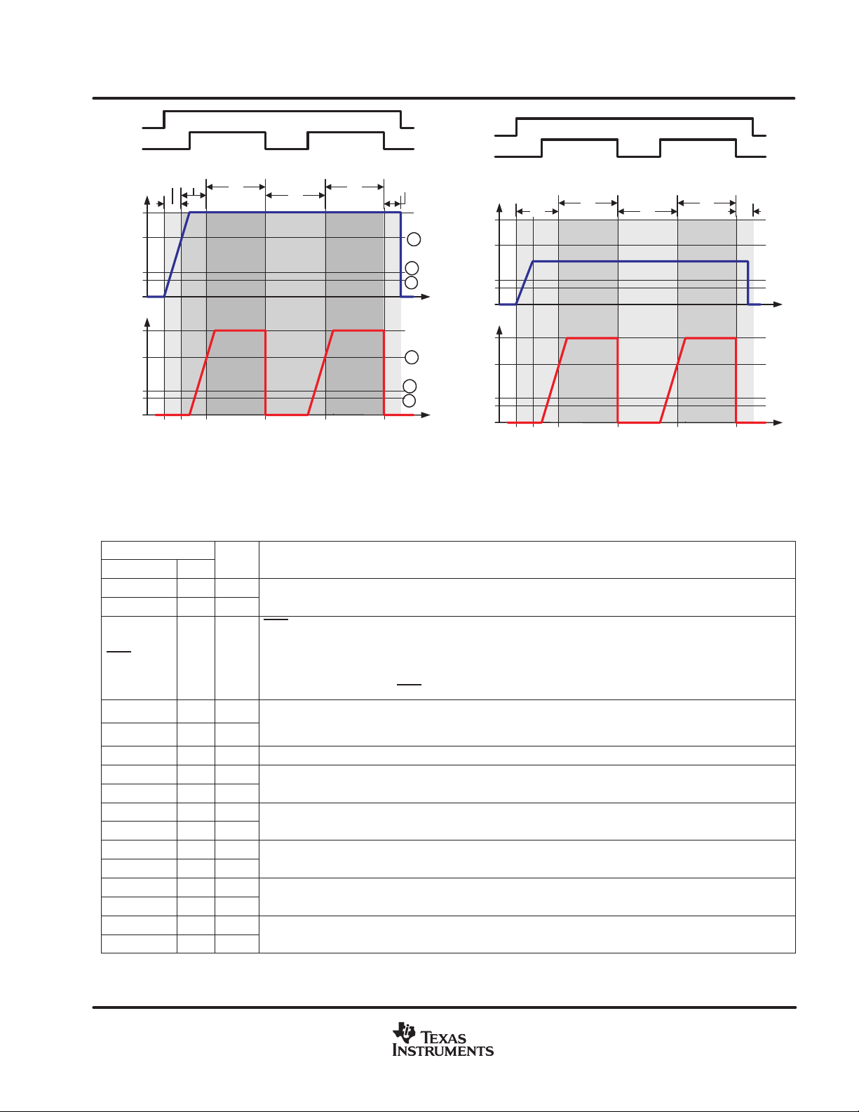
See waveform point A in Figure 1
(8)
See waveform point B in Figure 1
(9)
See waveform point C in Figure 1
SSTRTx charge current V
SSTRTx discharge current V
SSTRTx at SMPS regulation point voltage
SSTRTx OK to restart voltage 0.23 0.29 0.35
SSTRTx finished voltage
SSTRTx frequency select voltage
Forward voltage
Reverse current V
OUTx_U source impedance 3 10
OUTx_D source impedance 3 10
OUTx_U sink impedance 2.5 5.0
OUTx_D sink impedance 2.5 5.0
Gate non-overlap dead time 100 ns
= K1×VIN+B1, V
OFFSET
=K2×VIN×+B2 where K1=0.017, K2=0.01, B1=0.35 V, B2=0.4 V.
COMP
= 0.1 µF, C
VIN
(8)
(9)
should be approximately: V
VREG5
(7)
= 2.2 µF, C
SSTRTx
SSTRTx
(V
VREF5
TA = 25°C
RBST
= 0.01 µF, PGOOD = 0.2 V, ENBLx = DDR = VIN,
REF_X
TEST CONDITIONS MIN TYP MAX UNIT
= 1 V 1.8 2.3 2.9 µA
= 0.5 V 0.1 mA
− V
= 30 V 0.1 0.5 µA
COMP
VBSTx
+ V
OUT
), V
VREF5
ǒ
K1 )
(OUTx_U, OUTx_D)
= 5 V , IF = 10 mA
B1
Ǔ
(
)
VIN
K2 VIN ) B2
=1 nF, REG5_IN = 0V, GND =
1.00 1.22 1.45
1.4 1.5 1.6
3.35 3.60 3.80
0.80 0.85 V
)
V
Ω
Table 1. Frequency Selection
SSTRT1 SSTRT2 FREQUENCY (kHz)
C
1 MΩ || C
C
1 MΩ || C
(10)
Although selection is made by placing a 1M resistor in parallel with the SSTRTx timing
capacitor, the softstart time to 0.85V is altered by about only 20%.
6
only C
SSTRT
to GND C
SSTRT
only 1 MΩ || C
SSTRT
to GND 1 MΩ || C
SSTRT
only 450
SSTRT
only 360
SSTRT
SSTRT
SSTRT
www.ti.com
to GND 360
to GND 270
(10)
I/O
DESCRIPTION
f
that channel attempts to turn on. If both ENBL1 and ENBL2 are low then the 10-V (or (VO1_VDDQ)/2 output)
ENBL1
ENBL2
5.0
3.6
1.5
1.2
0
5.0
− Soft-Start Voltage − V
3.6
SSTRT
V
1.5
1.2
0
fSW − Switching Frequency − kHz
270 360
t1t0 t3t2 t4 t5
470
360
SSTRT1
470 270
SSTRT2
t − Time
R
SSTRT1
= R
SSTRT2
= OPEN = 450 kHz
Figure 1
SLUS564C − JULY 2003 − REVISED OCTOBER 2008
ENBL1
ENBL2
fSW − Switching Frequency − kHz
5.0
C
B
A
C
B
A
3.6
1.5
1.2
0
5.0
− Soft-Start Voltage − V
3.6
SSTRT
V
1.5
1.2
0
270
t1t0 t3t2 t4 t5
360
270
SSTRT1
t − Time
R
SSTRT1
= 1 MΩ, R
SSTRT2
Figure 2
360
270
SSTRT2
= OPEN = 360 kHz
TERMINAL FUNCTIONS
TERMINAL
NAME NO.
COMP1 2 O
COMP2 14 O
DDR 6 I
ENBL1 9 I
ENBL2 10 I
GND 7 O Signal ground pin.
INV1 1 I
INV2 15 I
LL1 28 I/O
LL2 18 I/O
OUT1_D 27 O
OUT2_D 19 O
OUT1_U 29 O
OUT2_U 17 O
OUTGND1 26 O
OUTGND2 20 O
Error amplifier output. Connect feedback network to this pin and INVx for compensation of control loop.
DDR selection pin. If this pin is grounded, the device runs in DDR Mode. The error amplifier reference for VO2
is (VO1_VDDQ)/2, the REF_X output voltage becomes (VO1_VDDQ)/2 and skip mode is disabled for VO2,
Also, VREG5 is turned off when both ENBLx are at low in this mode. If this pin is at 2.2-V or higher, the device
runs in ordinary dual SMPS mode (dual mode), then the error amplifier reference for VO2 is connected to internal 0.85-V reference, the REF_X output voltage becomes 10 V, VREG5 is kept on regardless of ENBLx status.
CAUTION: Do not toggle DDR
TTL Enable Input. If ENBLx is greater than 2.2 V, then the VREG5 is enabled (DDR mode) and the SMPS o
voltage as well as the oscillator are turned off. (See Table 2)
Error amplifier inverting input. Also input for skip comparator, and OVP/UVP comparators.
Switch-node connection for high-side driver and overcurrent protection circuitry.
Synchronous N-channel MOSFET driver output.
High-side N-channel MOSFET driver output.
Ground return for OUTx_D.
while ENBL1 or ENBL2 are high. (See Table 2)
www.ti.com
7
I/O
DESCRIPTION
t
time. A constant current fed to this capacitor ramps the reference during startup. Frequency selection is de-
time. A constant current fed to this capacitor ramps the reference during startup. Frequency selection is de-
the channel can start-up again. If DDR is low, then the VO1_VDDQ pin must be connected to the VDDQ output
-
SLUS564C − JULY 2003 − REVISED OCTOBER 2008
TERMINAL FUNCTIONS (continued)
TERMINAL
NAME NO.
Power good output. This is an open drain pull-down pin for power good. It remains low during soft-start until
PGOOD 12 O
REF_X 8 O
REG5_IN 21 I
SSTRT1 3 I
SSTRT2 13 I
SKIP 4 I
TRIP1 25 I
TRIP2 23 I
VBST1 30 I
VBST2 16 I
VO1_VDDQ 5 I
VO2
VREG5 22 O Internal, 60-mA, 5-V regulator output. DDR, ENBL1 or ENBL2 high ( > 2.2V) turns on the 5 V regulator.
VIN 24 I
11 I
both outputs become within ±7.5%. If INV1 or INV2 is out of regulation, or VREG5V goes under UVLO then this
pin goes low. The internal delay timer counts 2048 clks at low to high (by design, no delay for high to low). If
ENBLx is low, and the power good output is high, then the power good signal for that channel is ignored.
10-V N-channel MOSFET bias or (VO1_VDDQ)/2 reference output. If dual mode is selected (DDR > 2.2 V)
then this pin provides a low 10-V current (< 2 mA) bias, dropped down from VIN, for the SO – S5 switched
N-channel MOSFETs. If DDR mode is selected (DDR
of 3 mA source current. This bias/reference is shut off when ENBL1 and ENBL2 are both low. (See Table 2)
External 5V regulator Input. If this pin is above 4.7 V, then the 5 V circuit bias switches from the VREF5 to the
supply presented to REG5_IN.
Soft-start/frequency select input. Connect a capacitor between SSTRTx and ground for adjusting the softstar
scribed in Table 1. The soft-start capacitor is discharged upon UVLO/OVP/UVP, or when ENBLx is asserted
low.
Skip mode selection pin. Ground for automatic control between PWM mode in heavy load and hysteretic operation in light load. Tie high for PWM only operation for the entire load condition. If DDR
mode is disabled for Channel 2.
Channel 1 overcurrent trip point voltage input. Connect a resistor between TRIP1 and the high-side N-channel
MOSFET input conversion voltage for high-side N-channel MOSFET UVP current limit shut down. Connect
resistor between TRIP1 and GND for low-side N-channel MOSFET overcurrent latch shutdown.
Channel 2 overcurrent trip point voltage input. Connect a resistor between TRIP2 and the high-side N-channel
MOSFET input conversion voltage for high-side N-channel MOSFET UVP current limit shut down with a 180°
channel phase shift. Connect resistor between TRIP2 and GND for low-side N-channel MOSFET over current
latch shut-down. The oscillator voltage ramp adjustment (the feed-forward feature) for channel 2 is disabled
when this pin is tied to ground via a resistor.
Supply Input for high-side N-channel FET driver. Typically connected via charge pump from LLx.
Output discharge pin. Connect this pin to the SMPS output. The output is discharged to at least 0.3 V before
since this pin works as the VDDQ feedback to generate the VTT reference voltage and VO2 should be con
nected to GND since VTT must remain in a high-impedance state during S3 mode.
High-voltage input. Typically the battery voltage. This pin serves as inputs for the VREF5 regulator, the REF_X
regulator and positive input for overcurrent comparators. Precaution should be taken for tracing between this
pin and the high-side N-channel MOSFET drain where positive node of TRIPx resistors are located.
= GND) then this pin becomes (VO1_VDDQ)/2 capable
is grounded, then skip
Table 2. Reference Regulator Control
MODE DDR ENBL1 ENBL2 VREF5 REF_X OSC
DDR LOW LOW LOW OFF OFF OFF
DDR LOW LOW HIGH ON
DDR LOW HIGH LOW ON
DDR LOW HIGH HIGH ON
DUAL HIGH LOW LOW ON OFF OFF
DUAL HIGH LOW HIGH ON 10 V ON
DUAL HIGH HIGH LOW ON 10 V ON
DUAL HIGH HIGH HIGH ON 10 V ON
8
www.ti.com
OFF
VO1_DDR
2
VO1_DDR
2
ON
ON
ON
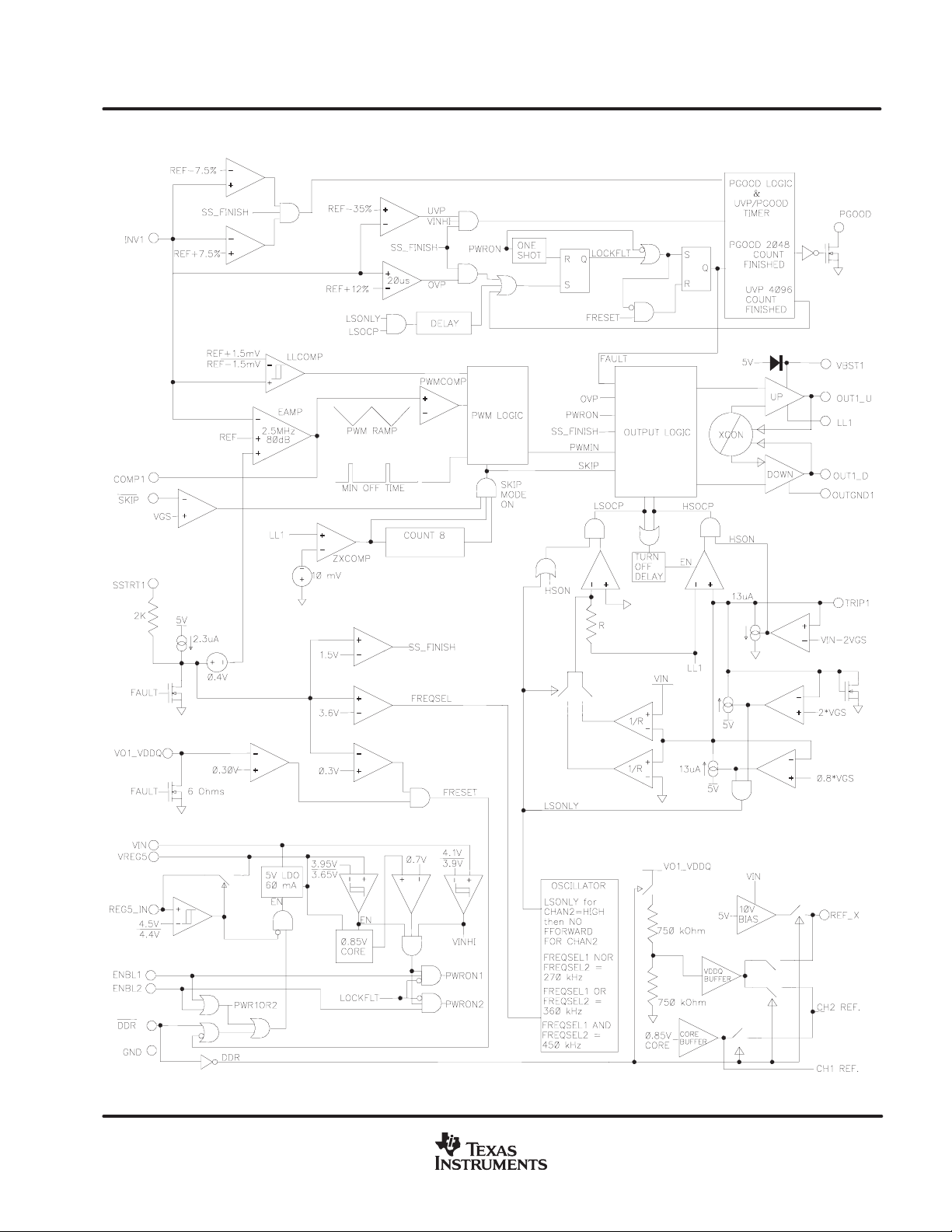
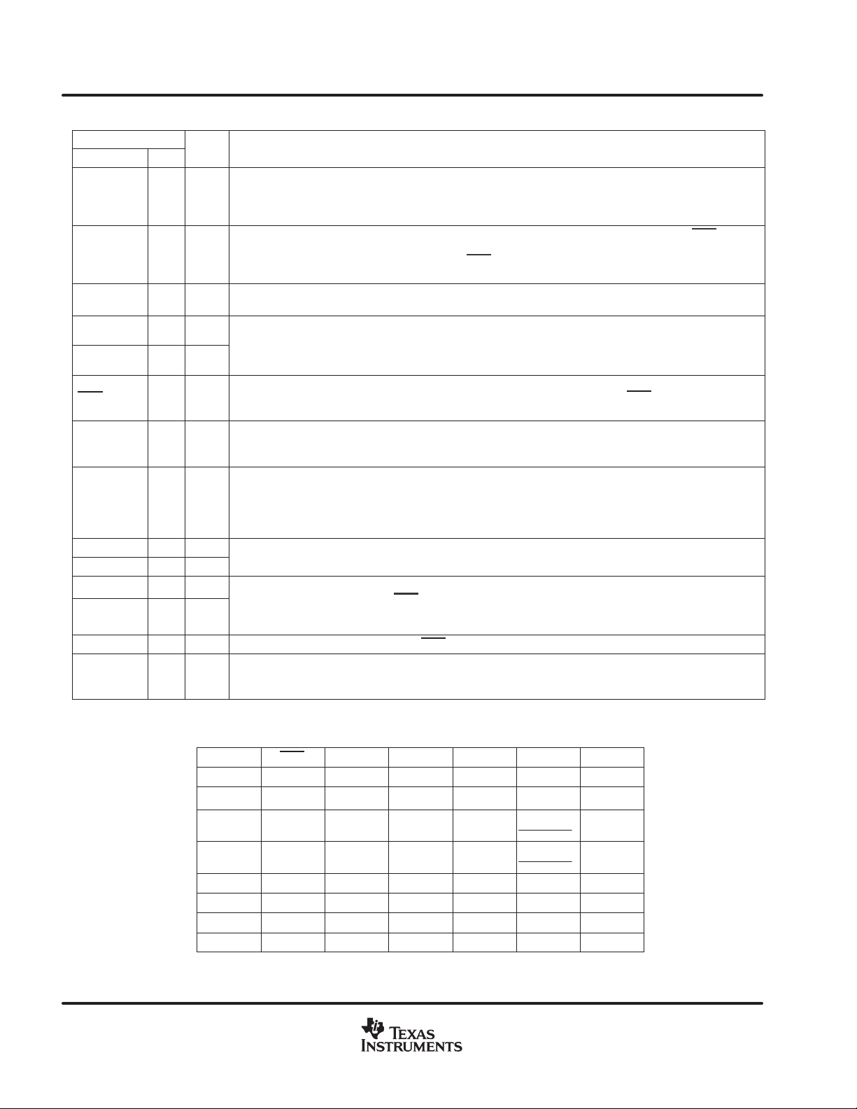
FUNCTIONAL BLOCK DIAGRAM
SLUS564C − JULY 2003 − REVISED OCTOBER 2008
Shows Channel 1 (VO1_VDDQ) and the supporting circuitry.
www.ti.com
9
 Loading...