

Page 1
1
2
3
4
19
18
17
16
SYNC
PGD
LVBP
RT
SA−
SAO
GND
SS
TPS40075
15
14
13
12
KFF
ILIM
VDD
HDRV
5
6
7
8
FB
COMP
PGND
LDRV
9 DBP
20
SA+
10
SW11BOOST
SYNC IN
PowerGood OUT
UDG−04075
V
IN
V
OUT
+
V
OUT
−
V
OUT
−
(at Load)
V
OUT
+
(at Load)
www.ti.com
SLUS676A – MAY 2006 – REVISED SEPTEMBER 2007
TPS40075
MIDRANGE INPUT SYNCHRONOUS BUCK CONTROLLER
WITH VOLTAGE FEED-FORWARD
1
FEATURES
2
• Operation Over 4.5-V to 28-V Input Range
• Fixed-Frequency Voltage-Mode Controller
• Integrated Unity Gain Amplifier for Remote
Output Sensing
• Predictive Gate Drive™ Generation II for
Improved Efficiency
• <1% Internal 700-mV Reference
• Input Voltage Feed Forward Control
• Prebiased Output Compatible
• Internal Gate Drive Outputs for High-Side and
Synchronous N-Channel MOSFETs
• Switching Frequency Programmable to 1 MHz
• 20-Pin QFN Package
• Thermal Shutdown Protection
• Software Design Tool and EVM Available
APPLICATIONS
• Power Modules
• Networking/Telecom
• Industrial
• Servers
The TPS40075 drives external N-channel MOSFETs
using second generation Predictive Gate Drive to
minimize conduction in the body diode of the low side
FET and maximize efficiency. Pre-biased outputs are
supported by not allowing the low side FET to turn on
until the voltage commanded by the closed loop soft
start is greater than the pre-bias voltage. Voltage
feed forward provides good response to input
transients and provides a constant PWM gain over a
wide input voltage operating range to ease
compensation requirements. Programmable short
circuit protection provides fault current limiting and
hiccup recovery to minimize power dissipation with a
shorted output. The 20-pin QFN package gives good
thermal performance and a compact footprint.
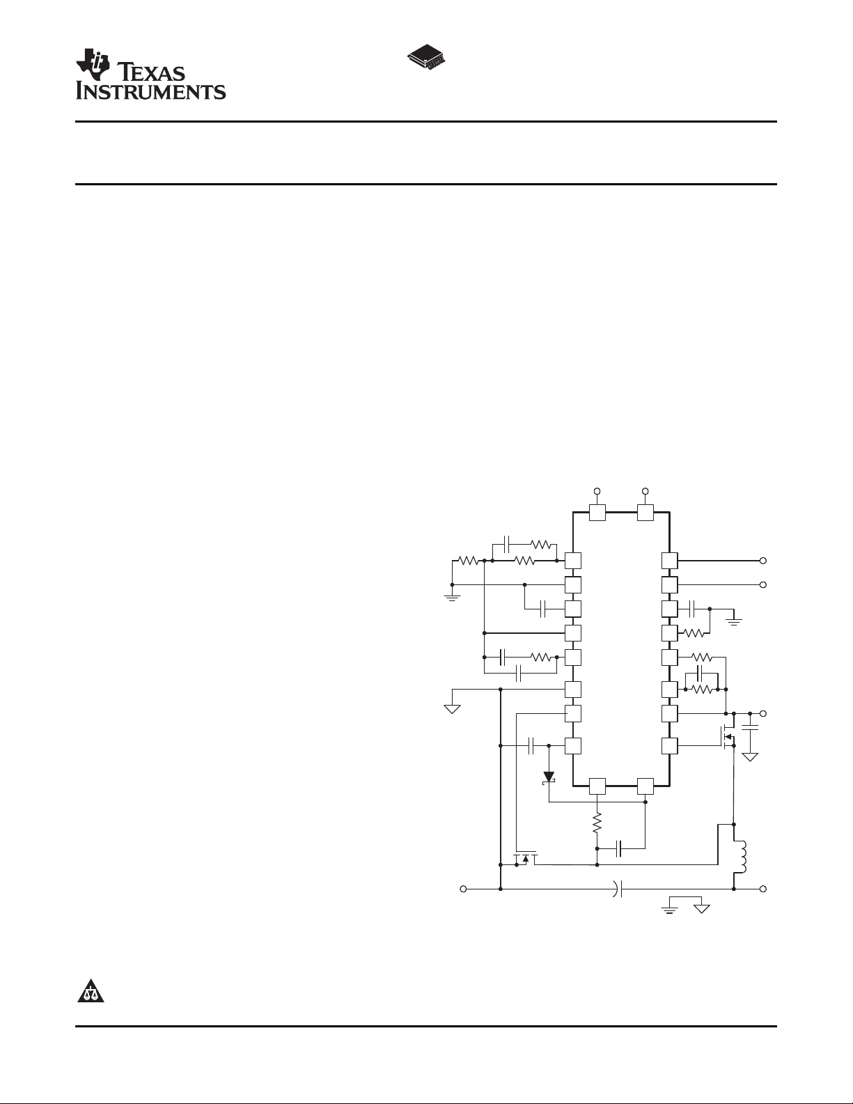
SIMPLIFIED APPLICATION DIAGRAM
CONTENTS
Device Ratings 2
Electrical Characteristics 4
Terminal Information 12
Application Information 15
Design Example 26
Additional References 40
DESCRIPTION
The TPS40075 is a mid voltage, wide input (4.5-V to
28-V), synchronous, step-down controller, offering
design flexibility for a variety of user programmable
functions, including; soft start, UVLO, operating
frequency, voltage feed-forward and high-side FET
sensed short circuit protection.
1
Please be aware that an important notice concerning availability, standard warranty, and use in critical applications of
Texas Instruments semiconductor products and disclaimers thereto appears at the end of this data sheet.
2 Predictive Gate Drive is a trademark of Texas Instruments.
PRODUCTION DATA information is current as of publication date.
Products conform to specifications per the terms of the Texas
Instruments standard warranty. Production processing does not
necessarily include testing of all parameters.
Copyright © 2006 – 2007, Texas Instruments Incorporated
Page 2
www.ti.com
TPS40075
SLUS676A – MAY 2006 – REVISED SEPTEMBER 2007
ORDERING INFORMATION
T
A
40 ° C to 85 ° C Plastic QFN (RHL)
(1) The TPS40075 is available taped and reeled only. Add an T suffix (i.e. TPS40075RHLT) to the orderable part number for quantities of
250 units per small reel. .
(2) Add an R suffix (i.e. TPS40075RHLR) to the orderable part number for quantities of 3,000 units per large reel.
DEVICE RATINGS
PACKAGE PART NUMBER
TPS40075RHLT
TPS40075RHLR
(1)
(2)
ABSOLUTE MAXIMUM RATINGS
over operating free-air temperature range unless otherwise noted
VDD, ILIM 30
FB, KFF, PGD, SYNC – 0.3 to 6
V
V
I
I
I
T
T
Input voltage range
DD
Output voltage range V
OUT
Output current source LDRV, HDRV 1.5
OUT
Output current sink
OUT
Output current source
OUT
Operating junction temperature range – 40 to 125
J
Storage temperature – 55 to 150
stg
(1) Stresses beyond those listed under "absolute maximum ratings" may cause permanent damage to the device. These are stress ratings
only, and functional operation of the device at these or any other conditions beyond those indicated under "recommended operating
conditions" is not implied. Exposure to absolute-maximum-rated conditions for extended periods may affect device reliability.
SW – 0.3 to 40 V
SA+, SA- – 0.3 to 11
SW, transient < 50 ns – 2.5
SW, transient – 125 V × ns
COMP, RT, SS – 0.3 to 6
BOOST, HDRV 50
DBP, SAO, LDRV 10.5
LVBP 6
LDRV, HDRV 2.0
KFF 10
RT 1 mA
LVBP 1.5
(1)
TPS40075 UNIT
A
° C
2 Submit Documentation Feedback Copyright © 2006 – 2007, Texas Instruments Incorporated
Product Folder Link(s) :TPS40075
Page 3
www.ti.com
TPS40075
SLUS676A – MAY 2006 – REVISED SEPTEMBER 2007
RECOMMENDED OPERATING CONDITIIONS
MIN NOM MAX UNIT
V
T
ELECTROSTATIC DISCHARGE (ESD) PROTECTION
Human body model 1500 V
CDM 1500
Input voltage 4.5 28 V
DD
Operating free-air temperature -40 85 ° C
A
PARAMETER MIN TYP MAX UNIT
PACKAGE DISSIPATION RATINGS
THERMAL IMPEDANCE
AIRFLOW (LFM) JUNCTION-TO-AMBIENT TA= 25 ° C POWER RATING (W) TA= 85 ° C POWER RATING (W)
Natural Convection 42 2.38 0.95
200 35 2.85 1.14
400 31 3.22 1.29
(1) For more information on the RHL package and the test method, refer to TI technical brief, literature number SZZA017. The ratings in this
table are for the JEDEC High-K board.
(1)
( ° C/W)
Copyright © 2006 – 2007, Texas Instruments Incorporated Submit Documentation Feedback 3
Product Folder Link(s) :TPS40075
Page 4
www.ti.com
TPS40075
SLUS676A – MAY 2006 – REVISED SEPTEMBER 2007
ELECTRICAL CHARACTERISTICS
TA= – 40 ° C to 85 ° C, V
(unless otherwise noted)
INPUT SUPPLY
V
DD
OPERATING CURRENT
I
DD
LVBP
V
LVBP
OSCILLATOR/RAMP GENERATOR
f
OSC
V
RT
t
ON(min)
V
IH
V
IL
I
SYNC
V
KFF
I
KFF
SOFT START
I
SS
t
DSCH
t
SS
V
SSSD
V
SSEN
V
SSSDHYS
DBP
V
DBP
ERROR AMPLIFIER
V
FB
V
SS(offset)
GBWP Gain bandwidth
A
VOL
I
SRC
I
SINK
I
BIAS
SHORT CIRCUIT CURRENT PROTECTION
I
ILIM
V
ILIM(ofst)
t
HSC
t
BLANK
Input voltage range, VIN 4.5 28 V
Quiescent current Output drivers not switching 2.5 3.5 mA
Output voltage TA= TJ= 25 ° C 3.9 4.2 4.5 V
Accuracy 450 500 550 kHz
RT voltage 2.23 2.40 2.58 V
Minimum output pulse time
High-level input voltage, SYNC 2 5
Low-level input voltage, SYNC 0.8
Input current, SYNC 5 10 µA
Maximum duty cycle
Feed-forward voltage 0.35 0.40 0.45 V
Feed-forward current operating range
Charge current 9.5 12 14.5 µA
Discharge time C
Soft-start time 210 290 500
Shutdown threshold, V
Enable threshold, V
Shutdown threshold hysteresis 35 130
Output voltage V
Feedback regulation voltage total variation 0 ° C ≤ TA= TJ≤ 85 ° C 0.690 0.700 0.707
Soft-start offset from VSS
Open loop gain 50 dB
Output source current 2.5 4.5
Output sink current 2.5 6
Input bias current V
Current sink into ILIM pin 115 135 150 µA
Current limit offset voltage V
Minimum HDRV pulse width During short circuit 135 225 ns
Propagation delay to output
Blanking time
= 12 Vdc, RT= 90.9 k Ω , I
IN
PARAMETER TEST CONDITIONS MIN TYP MAX UNIT
SS
rising 310 410 mV
SS
(1)
(1)
= 300 µA, fSW= 500 kHz, all parameters at zero power dissipation
KFF
(1)
(1)
C
= 0 nF 150 ns
HDRV
V
= 0 V, 100 kHz ≤ fSW≤ 500 kHz 84% 95%
FB
V
= 0 V, fSW= 1 MHz 76% 93%
FB
20 1100 µA
= 3.9 nF 25 75
SS
C
V
= 3.9 nF, V
SS
rising from 0.7 V to 1.6
SS
falling 225 275 325
V
> 10 V 7 8 9
DD
V
VDD
= 4.5 V, I
= 25 mA 4.0 4.3
OUT
TA= TJ= 25 ° C 0.698 0.700 0.704
-40 ° C ≤ TA= TJ≤ 85 ° C 0.690 0.700 0.715
(1)
Offset from V
to error amplifier 1
SS
5 10 MHz
= 0.7 V – 250 0 nA
FB
= 11.5 V, (V
ILIM
(1)
- V
) V
SW
ILIM
= 12 V – 50 – 30 – 10 mV
VDD
50 ns
50 ns
V
µs
V
mA
(1) Ensured by design. Not production tested.
4 Submit Documentation Feedback Copyright © 2006 – 2007, Texas Instruments Incorporated
Product Folder Link(s) :TPS40075
Page 5
www.ti.com
ELECTRICAL CHARACTERISTICS (continued)
TA= – 40 ° C to 85 ° C, V
(unless otherwise noted)
t
OFF
V
SW
t
PC
V
ILIM(pre)
OUTPUT DRIVERS
t
HFALL
t
HRISE
t
HFALL
t
HRISE
t
LFALL
t
LRISE
t
LFALL
t
LRISE
V
OH
V
OL
V
OH
V
OL
BOOST REGULATOR
V
BOOST
UVLO
V
UVLO
POWER GOOD
V
PGD
V
FBH
V
FBL
SENSE AMPLIFIER
V
IO
A
DIFF
V
ICM
R
G
I
OH
I
OL
GBWP Gain bandwidth
THERMAL SHUTDOWN
Off time during a fault (SS cycle times) 7 cycles
Switching level to end precondition
Precondition time
Current limit precondition voltage threshold
High-side driver fall time
High-side driver rise time
High-side driver fall time
High-side driver rise time
Low-side driver fall time
Low-side driver rise time
Low-side driver fall time
Low-side driver rise time
High-level output voltage, HDRV V
Low-level output voltage, HDRV V
High-level output voltage, LDRV V
Low-level output voltage, LDRV V
Output voltage V
Programmable UVLO threshold voltage R
Programmable UVLO hysteresis R
Fixed UVLO threshold voltage Turn-on, V
Fixed UVLO hysteresis 275 365 mV
Powergood voltage I
High-level output voltage, FB 770 mV
Low-level output voltage, FB 630
Input offset voltage -9 9 mV
Differential gain V
Input common mode range
Internal resistance for setting gain 14 20 26 k Ω
Output source current 2 10 15
Output sink current 15 25 35
= 12 Vdc, RT= 90.9 k Ω , I
IN
PARAMETER TEST CONDITIONS MIN TYP MAX UNIT
(2)
(4)
TPS40075
SLUS676A – MAY 2006 – REVISED SEPTEMBER 2007
= 300 µA, fSW= 500 kHz, all parameters at zero power dissipation
KFF
(1)
(2)
(2)
(2)
(2)
(2)
(2)
(2)
(2)
(3)
(V
- V
VDD
) 2 V
SW
100 ns
(2)
C
= 2200 pF, (HDRV - SW) ns
HDRV
C
= 2200 pF, (HDRV - SW)
HDRV
V
= 4.5 V
VDD
C
= 2200 pF ns
LDRV
C
= 2200 pF, VDD= 4.5 V ns
LDRV
I
= -0.01 A, (V
HDRV
I
= -0.1 A, (V
HDRV
(V
- V
HDRV
(V
HDRV
(V
DBP
(V
DBP
I
LDRV
I
LDRV
VDD
KFF
KFF
PGD
V
SA+
SA+ and SA-
SA+
), I
SW
- V
), I
SW
- V
), I
LDRV
- V
), I
LDRV
= 0.01 A 0.03 0.05
= 0.1 A 0.3 0.5
= 12 V 15.2 17.0 V
= 90.9 k Ω , turn-on, V
= 90.9 k Ω 1.10 1.55 2.00 V
rising 4.15 4.30 4.45
VDD
= 1 mA 370 550
= V
= 1.25 V, Offset referenced to
SA-
- V
= 4.5 V 0.995 1.000 1.005
SA-
- V
BOOST
BOOST
= 0.01A 0.06 0.10
HDRV
= 0.1 A 0.65 1.00
HDRV
= -0.01A 0.65 1.00
LDRV
= -0.1 A 0.875 1.300
LDRV
) 0.7 1.0
HDRV
- V
) 0.95 1.35
HDRV
rising 6.2 7.2 8.2
VDD
6.8 V
36
48
72
96
24
48
48
96
ns
0 6 V
mA
2 MHz
(2) Ensured by design. Not production tested.
(3) 3 V at internal amplifier terminals, 6 V at SA+ and SA- pins.
(4) Ensured by design. Not production tested.
Copyright © 2006 – 2007, Texas Instruments Incorporated Submit Documentation Feedback 5
Product Folder Link(s) :TPS40075
Page 6
www.ti.com
TJ − Junction Temperature − °C
V
LVPP
− LVBP Voltage − V
−50 −25 50 100 1250
4.15
4.10
4.30
4.20
4.25
4.05
4.00
25 75
VDD = 28 V
VDD = 12 V
−50 −25 50 100 1250
8.00
7.90
8.15
8.05
8.10
7.85
7.80
25 75
7.95
V
DBP
− DBP Voltage − V
VDD = 28 V
VDD = 12 V
TJ − Junction Temperature − °C
TPS40075
SLUS676A – MAY 2006 – REVISED SEPTEMBER 2007
ELECTRICAL CHARACTERISTICS (continued)
TA= – 40 ° C to 85 ° C, V
(unless otherwise noted)
Shutdown temperature threshold
Hysteresis
= 12 Vdc, RT= 90.9 k Ω , I
IN
PARAMETER TEST CONDITIONS MIN TYP MAX UNIT
(4)
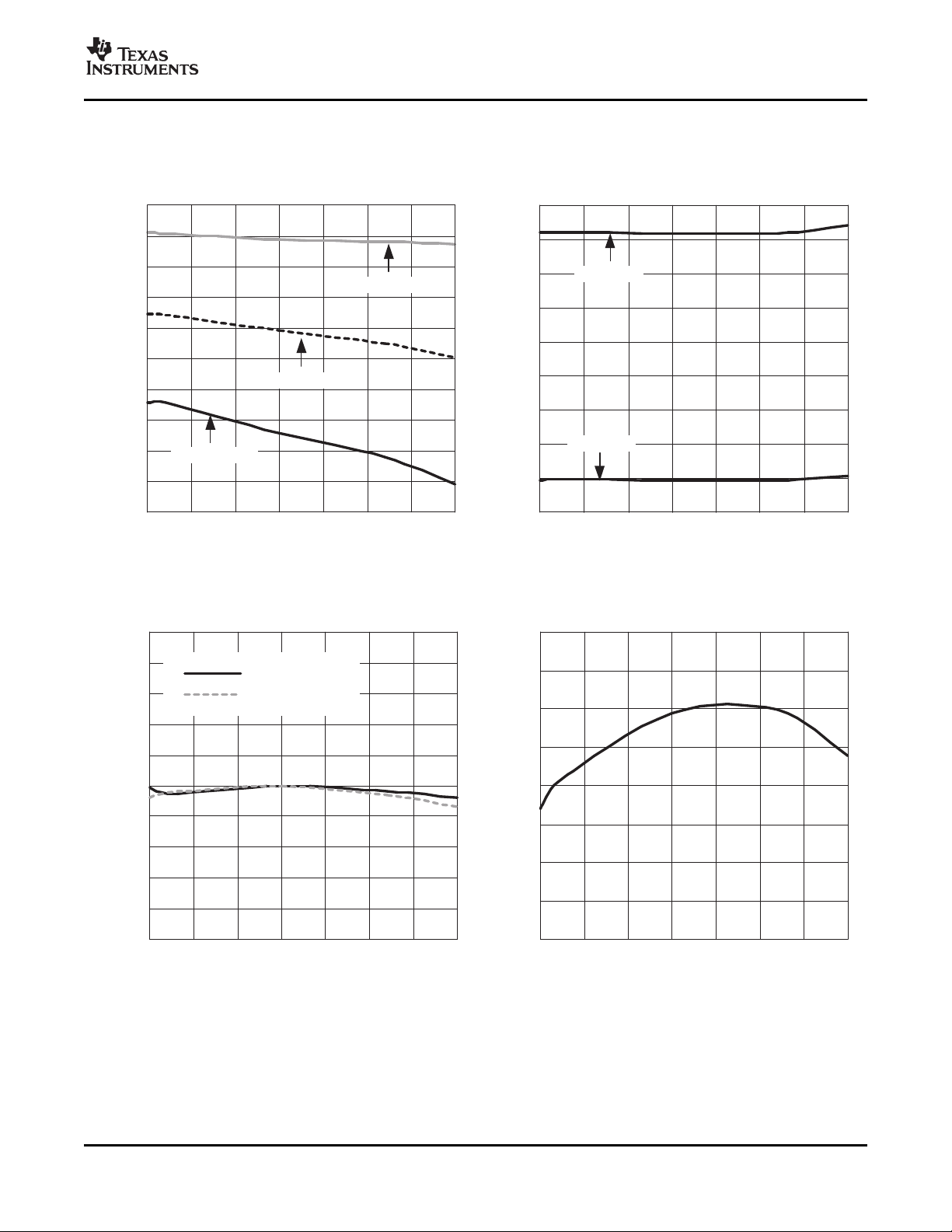
LVBP VOLTAGE DBP VOLTAGE
JUNCTION TEMPERATURE JUNCTION TEMPERATURE
vs vs
= 300 µA, fSW= 500 kHz, all parameters at zero power dissipation
KFF
(4)
165
15
° C
TYPICAL CHARACTERISTICS
Figure 1. Figure 2.
6 Submit Documentation Feedback Copyright © 2006 – 2007, Texas Instruments Incorporated
Product Folder Link(s) :TPS40075
Page 7
www.ti.com
−50 −25 50 100 1250
4.46
4.43
4.50
4.48
4.49
4.41
4.40
25 75
4.44
4.42
4.47
4.45
V
DBP
− DBP Voltage − V
VDD = 4.5 V
I
LOAD
= 25 mA
TJ − Junction Temperature − °C
V
DROP
− Bootstrap Diode Voltage Drop − V
TJ − Junction Temperature − °C
−50 −25 50 100 1250
1.6
1.3
2.0
1.7
1.9
1.1
1.0
25 75
1.4
1.8
1.5
1.2
−50 −25 50 100 1250
115
150
140
100
25 75
135
125
110
105
120
145
130
I
ILIM
− Current Limit Sink Current − µA
TJ − Junction Temperature − °C
VDD
28 V
12 V
4.5 V
V
ILIM(offst)
– Current Limit Offset Voltage Drop – mV
TJ – Junction Temperature – °C
−50 −25 50 100 1250
−40
0
−10
−60
25 75
−20
−30
−50
Average
+3 S
−3 S
TYPICAL CHARACTERISTICS (continued)
DBP VOLTAGE BOOTSTRAP DIODE VOLTAGE
vs vs
JUNCTION TEMPERATURE JUNCTION TEMPERATURE
TPS40075
SLUS676A – MAY 2006 – REVISED SEPTEMBER 2007
Figure 3. Figure 4.
CURRENT LIMIT OFFSET VOLTAGE CURRENT LIMIT SINK CURRENT
vs vs
JUNCTION TEMPERATURE JUNCTION TEMPERATURE
Figure 5. Figure 6.
Copyright © 2006 – 2007, Texas Instruments Incorporated Submit Documentation Feedback 7
Product Folder Link(s) :TPS40075
Page 8
www.ti.com
−50 −25 50 100 1250
699
704
697
25 75
702
698
700
703
701
V
FB
− Feedback Voltage − V
TJ − Junction Temperature − °C
VDD
28 V
4.5 V
12 V
−50 −25 50 100 1250
0
30
−15
25 75
20
−10
5
25
10
−5
15
High Level Output Current
Low Level Output Current
I
SENSE
− Sense Amplifier Output Current − mA
TJ − Junction Temperature − °C
f
SW
− Switching Frequency − kHz
V
VDD
− Input Voltage − V
4 8 16 24 2812 20
500
490
497
491
493
498
496
494
499
495
492
RRT = 90.1kΩ
A
DIFF
− Sense Amplifier Gain − V/V
TJ − Junction Temperature − °C
−50 −25 50 100 1250 25 75
0.9965
0.9980
1.0005
0.9995
0.9970
0.9985
1.000
0.9990
0.9975
VDD = 4.5 V
VDD = 2.5 V
VDD = 1.25 V
VDD = 0.5 V
TPS40075
SLUS676A – MAY 2006 – REVISED SEPTEMBER 2007
TYPICAL CHARACTERISTICS (continued)
FEEDBACK REGULATION VOLTAGE SENSE AMPLIFIER OUTPUT CURRENT
vs vs
JUNCTION TEMPERATURE JUNCTION TEMPERATURE
Figure 7. Figure 8.
CURRENT SENSE AMPLIFIER GAIN SWITCHING FREQUENCY
vs vs
JUNCTION TEMPERATURE INPUT VOLTAGE
8 Submit Documentation Feedback Copyright © 2006 – 2007, Texas Instruments Incorporated
Figure 9. Figure 10.
Product Folder Link(s) :TPS40075
Page 9
www.ti.com
−50 −25 50 100 1250 25 75
4.35
3.90
4.20
3.95
4.30
4.15
4.05
4.00
4.25
4.10
TJ − Junction Temperature − °C
V
UVLO
− Undervoltage Lockout Threshold − V
V
UVLO(on)
V
UVLO(off)
TJ − Junction Temperature − °C
D
MAX
− Maximum Duty Cycle − %
−50 −25 50 100 1250 25 75
93
83
90
84
86
92
89
87
85
91
88
fSW = 100 kHZ
fSW = 500 kHZ
fSW = 1 MHZ
−50 −25 50 100 1250 25 75
1.10
0.90
1.04
0.92
0.96
1.08
1.02
0.98
0.94
1.06
1.00
TJ − Junction Temperature − °C
V
UVLO
− Relative Programmable UVLO Threshold − %
V
UVLO(on)
V
UVLO(off)
TJ − Junction Temperature − °C
I
SS
− Soft−Start Charging Current − µA
−50 −25 50 100 1250 25 75
14.0
10.0
10.5
11.0
13.5
12.5
11.5
13.0
12.0
TYPICAL CHARACTERISTICS (continued)
TPS40075
SLUS676A – MAY 2006 – REVISED SEPTEMBER 2007
MAXIMUM DUTY CYCLE UNDERVOLTAGE LOCKOUT
vs vs
JUNCTION TEMPERATURE JUNCTION TEMPERATURE
Figure 11. Figure 12.
PROGRAMMABLE UVLO THRESHOLD SOFTSTART CHARGING CURRENT
vs vs
JUNCTION TEMPERATURE JUNCTION TEMPERATURE
Figure 13. Figure 14.
Copyright © 2006 – 2007, Texas Instruments Incorporated Submit Documentation Feedback 9
Product Folder Link(s) :TPS40075
Page 10
www.ti.com
100
1.5
0.5
200 300 400 500 600 700 800 900 1000
1.0
3.0
2.0
2.5
3.5
5.0
4.0
4.5
VIN = 28 V
VIN = 24 V
VIN = 18 V
VIN = 15 V
VIN = 12 V
VIN = 10 V
VIN = 8 V
VIN = 5 V
f
OSC
− Oscillator Frequency − kHz
V
OUT
− Output Voltage − V
TJ − Junction Temperature − °C
I
BIAS
− Error Amplifier Input Bias Current − nA
−50 −25 50 100 1250 25 75
0
−90
−80
−70
−10
−30
−60
−20
−40
−50
VDD − Input Voltage − V
f
OSC
− Frequency − kHz
2 6 18 26 3010
500
495
505
520
510
515
490
485
480
14 22
fSW − Switching Frequency − kHz
0
100
0
200 400 600 800 1000
200
300
400
500
600
R
T
− Timing Resistance − kΩ
TPS40075
SLUS676A – MAY 2006 – REVISED SEPTEMBER 2007
TYPICAL CHARACTERISTICS (continued)
ERROR AMPLIFIER INPUT BIAS CURRENT MINIMUM OUTPUT VOLTAGE
vs vs
JUNCTION TEMPERATURE FREQUENCY
Figure 15. Figure 16.
SWITCHING FREQUENCY TYPICAL SWITCHING FREQUENCY
vs vs
TIMING RESISTANCE INPUT VOLTAGE
10 Submit Documentation Feedback Copyright © 2006 – 2007, Texas Instruments Incorporated
Figure 17. Figure 18.
Product Folder Link(s) :TPS40075
Page 11
www.ti.com
60 90 150 180 210 270120 240
4
2
8
6
10
14
12
18
16
20
R
KFF
− Feedforward Impedance − kΩ
V
UVLO
−
Programmable UVLO Threshold − V
UVLOV
ON
f
SW
= 500 kHz
UVLOV
OFF
R
KFF
− Feedforward Impedance − kΩ
100 150 250 300 350 450200 400
4
2
8
6
10
14
12
18
16
20
V
UVLO
−
Programmable UVLO Threshold − V
UVLOV
ON
f
SW
= 300 kHz
UVLOV
OFF
40 60 100 120 140 18080 160
4
2
8
6
10
14
12
18
16
20
R
KFF
− Feedforward Impedance − kΩ
V
UVLO
−
Programmable UVLO Threshold − V
UVLOV
ON
f
SW
= 750 kHz
UVLOV
OFF
8 16 20 24 28124
40
20
30
70
50
60
100
80
90
VIN − Input Voltage − V
Duty Cycle − %
UVLO
(on)
= 8 V
UVLO
(on)
= 15 V
UVLO
(on)
= 4.5 V
UVLO
(on)
= 12 V
TYPICAL CHARACTERISTICS (continued)
TPS40075
SLUS676A – MAY 2006 – REVISED SEPTEMBER 2007
UVLO THRESHOLD VOLTAGE UVLO THRESHOLD VOLTAGE
vs vs
FEEDFORWARD IMPEDANCE FEEDFORWARD IMPEDANCE
Figure 19. Figure 20.
UVLO THRESHOLD VOLTAGE TYPICAL MAXIMUM DUTY CYCLE
vs vs
FEEDFORWARD IMPEDANCE INPUT VOLTAGE
Copyright © 2006 – 2007, Texas Instruments Incorporated Submit Documentation Feedback 11
Figure 21. Figure 22.
Product Folder Link(s) :TPS40075
Page 12
www.ti.com
255 10 2015 30
4.10
4.00
4.05
4.15
4.20
4.35
4.25
4.30
4.40
4.45
4.50
VDD − Input Voltage − V
V
DBP
− Low Voltage Bypass Voltage − V
VDD − Input Voltage − V
V
DBP
− Driver Bypass Voltage − V
0
5
4
5 10 15 20 25
7
6
9
8
10
SAO
GND
SS
FB
COMP
PGND
LDRV
DBP
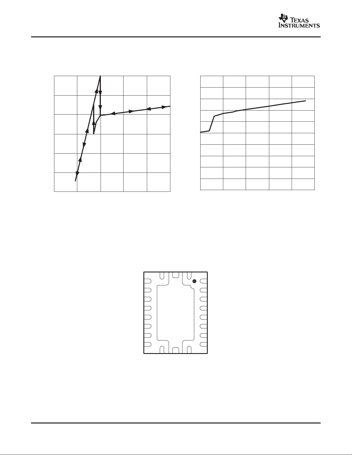
RHL PACKAGE
(BOTTOM VIEW)
SYNC
PGD
LVBP
RT
KFF
ILIM
VDD
HDRV
SA+
SA−
BOOST
SW
20 1
11 10
2
3
4
5
6
7
8
9
19
18
17
16
15
14
13
12
TPS40075
SLUS676A – MAY 2006 – REVISED SEPTEMBER 2007
INPUT VOLTAGE INPUT VOLTAGE
vs vs
DBP VOLTAGE LOW VOLTAGE BYPASS VOLTAGE
TYPICAL CHARACTERISTICS (continued)
Figure 23. Figure 24.
TERMINAL INFORMATION
12 Submit Documentation Feedback Copyright © 2006 – 2007, Texas Instruments Incorporated
Product Folder Link(s) :TPS40075
Page 13
www.ti.com
TPS40075
SLUS676A – MAY 2006 – REVISED SEPTEMBER 2007
Table 1. TERMINAL FUNCTIONS
TERMINAL
NAME NO.
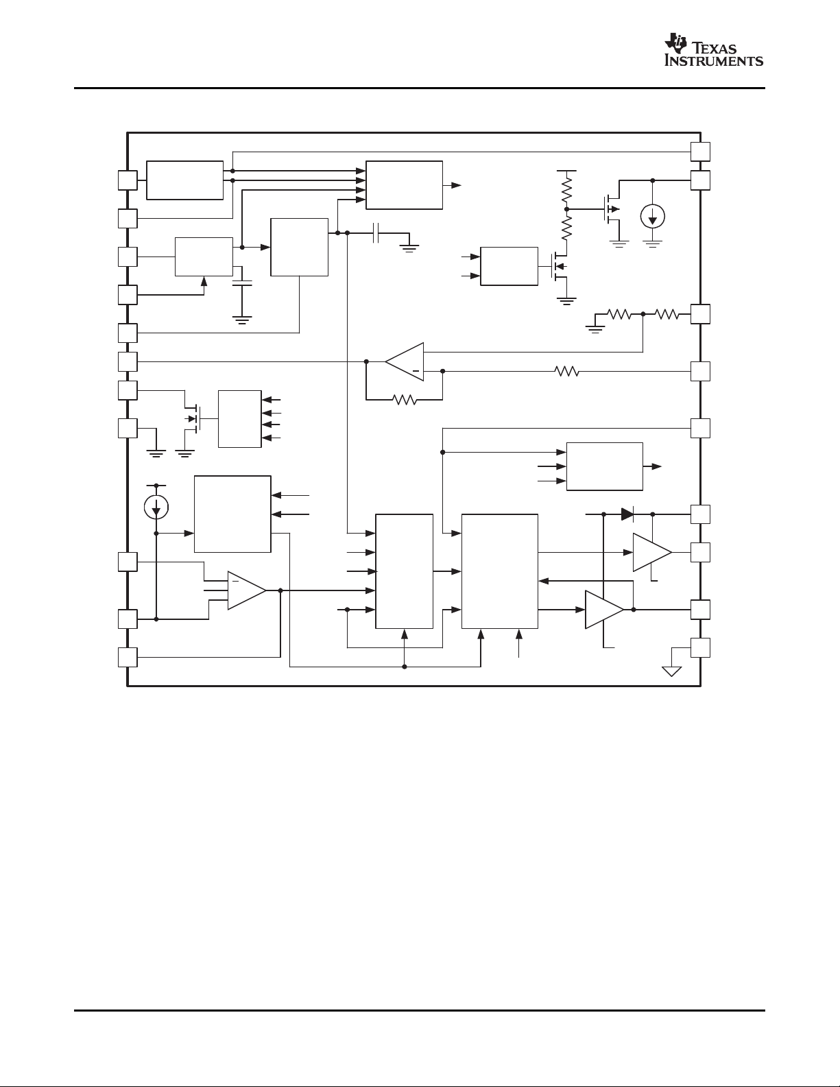
BOOST 11 I
COMP 6 O FB pin to compensate the overall loop. This pin is internally clamped to a 3.4-V maximum output drive capability
DBP 9 O
FB 5 I
GND 3 - Ground reference for the device.
HDRV 12 O
ILIM 14 I conduction. Just prior to the beginning of a switching cycle this pin is pulled to approximately V
KFF 15 I into this pin is used to control the slope of the PWM ramp and program undervoltage lockout. Nominal voltage at
LDRV 8 O
LVBP 17 O
PGD 18 O
PGND 7
RT 16 I A resistor is connected from this pin to GND to set the switching frequency.
SA+ 20 I Noninverting input of the remote voltage sense amplifier.
SA- 1 I Inverting input of the remote voltage sense amplifier.
SAO 2 O Output of the remote voltage sense amplifier.
SS 4 I
SW 10 I timing. This pin is also the return path from the high-side FET for the floating high-side FET driver. A 1.5- Ω resistor
SYNC 19 I Logic input for pulse train to synchronize oscillator.
VDD 13 I Supply voltage for the device.
I/O DESCRIPTION
The BOOST voltage is 8-V greater than the input voltage. The peak voltage on BOOST is equal to the SW node
voltage plus the voltage present at DBP less the bootstrap diode drop. This drop can be 1.4 V for the internal
bootstrap diode or 300 mV for an external schottkey diode. The voltage differential between this pin and SW is the
available drive voltage for the high-side FET.
Output of the error amplifier, input to the PWM comparator. A feedback network is connected from this pin to the
for quicker recovery from a saturated feedback loop situation.
8-V regulator output used for the gate drive of the N-channel synchronous rectifier and as the supply for charging
the bootstrap capacitor. This pin should be bypassed to ground with a 1.0-µF ceramic capacitor.
Inverting input to the error amplifier. In normal operation the voltage on this pin is equal to the internal reference
voltage, 0.7 V.
Floating gate drive for the high-side N-channel MOSFET. This pin switches from BOOST (MOSFET on) to SW
(MOSFET off).
Short circuit protection programming pin. This pin is used to set the overcurrent threshold. An internal current sink
from this pin to ground sets a voltage drop across an external resistor connected from this pin to VDD. The voltage
on this pin is compared to the voltage drop (V
when SW is within 2 V of V
capacitor across the resistor from ILIM to VDD allows the ILIM threshold to decrease during the switch on time,
or after a timeout (the precondition time) - whichever occurs first. Placing a
VDD
-V
VDD
) across the high side N-channel MOSFET during
SW
VDD
effectively programming the ILIM blanking time. See Applications Information section.
A resistor is connected from this pin to VDD programs the amount of input voltage feed-forward. The current fed
this pin is maintained at 400 mV.
Gate drive for the N-channel synchronous rectifier. This pin switches from DBP (MOSFET on) to PGND (MOSFET
off). For proper operation, the total gate charge of the MOSFET connected to LDRV should be less than 50nC.
4.2-V reference used for internal device logic and analog functions. This pin should be bypassed to GND with a
0.1-µF ceramic capacitor. External loads less than 1 mA and electrically quiet may be applied.
This is an open drain output that pulls to ground when soft start is active, or when the FB pin is outside a ± 10%
band around the 700 mV reference voltage.
Power ground reference for the device. There should be a low-impedance path from this pin to the source(s) of the
lower MOSFET(s).
Soft-start programming pin. A capacitor connected from this pin to GND programs the soft-start time. The
capacitor is charged with an internal current source of 12 µA. The resulting voltage ramp on the SS pin is used as
a second non-inverting input to the error amplifier. The voltage at this error amplifier input is approximately 1 V
less that that on the SS pin. Output voltage regulation is controlled by the SS voltage ramp until the voltage on the
SS pin reaches the internal offset voltage of 1 V plus the internal reference voltage of 700 mV. If SS is below the
internal offset voltage of 1 V (300 mV minimum ensured), the resulting output voltage is zero. Also provides timing
for fault recovery attempts. Pulling this pin below 250 mV causes the controller to enter a shutdown state with
HDRV and LDRV held in a low state.
This pin is connected to the switched node of the converter and used for overcurrent sensing as well as gate drive
in series with this pin is required for protection against substrate current issues.
/2 and released
Copyright © 2006 – 2007, Texas Instruments Incorporated Submit Documentation Feedback 13
Product Folder Link(s) :TPS40075
Page 14
www.ti.com
9
12
8
13
17
16
15
VDD
LVBP
RT
KFF
DBP
HDRV
LDRV
18
3
5
4
PGD
GND
FB
SS
6COMP
Reference
Regulator
Predictive
Gate Drive
Control
Logic
UVLO
Controller
Oscillator
14 ILIM
Pulse
Control
SW
CLK
10 SW
Overcurrent
Comparator
and Control
CLK
ILIM OC
7 PGND
11 BOOST
VDD
UVLO
Ramp
Generator
Power
Good
Logic
770 mV
FB
630 mV
SS Active
PWM
OC
CLK
UVLO
FAULT
IZERO
DBP
+
+
700 mV
RAMP
Soft Start
and
Fault Control
OC
CLK
SW
PGND
LVBP
2SAO
20 SA+
1 SA−
R
R
R
+
R
UDG−04076
19SYNC
TPS40075
TPS40075
SLUS676A – MAY 2006 – REVISED SEPTEMBER 2007
SIMPLIFIED BLOCK DIAGRAM
14 Submit Documentation Feedback Copyright © 2006 – 2007, Texas Instruments Incorporated
Product Folder Link(s) :TPS40075
Page 15

www.ti.com
13
7
14
12
10
8
ILIM
HDRV
SW
LDRV
VDD
PGND
TPS40075
C
R
VIN
UDG−05058
+
_
TPS40075
SLUS676A – MAY 2006 – REVISED SEPTEMBER 2007
APPLICATION INFORMATION
The TPS40075 allows the user to construct synchronous voltage mode buck converters with inputs ranging from
4.5 V to 28 V and outputs as low as 700 mV. Predictive gate drive circuitry optimizes switching delays for
increased efficiency and improved converter output power capability. Voltage feed-forward is employed to ease
loop compensation for wide input range designs and provide better line transient response.
An on-board unity gain differential amplifier is provided for remote sensing in applications that require the tightest
load regulation. The TPS40075 incorporates circuitry to allow startup into a pre-existing output voltage without
sinking current from the source of the pre-existing output voltage. This avoids damaging sensitive loads at
startup. The controller can be synchronized to an external clock source or can free run at a user programmable
frequency. An integrated power good indicator is available for logic (open drain) output of the condition of the
output of the converter.
MINIMUM PULSE WIDTH
The TPS40075 has limitations on the minimum pulse width that can be used to design a converter. Reliable
operation is guaranteed for nominal pulse widths of 150 ns and above. This places some restrictions on the
conversion ratio that can be achieved at a given switching frequency. See Figure 16 .
SLEW RATE LIMIT ON VDD
The regulator that supplies power for the drivers on the TPS40075 requires a limited rising slew rate on VDD for
proper operation if the input voltage is above 10 V. If the slew rate is too great, this regulator can over shoot and
damage to the part can occur. To ensure that the part operates properly, limit the slew rate to no more than
0.12 V/ μ s as the voltage at VDD crosses 8 V. If necessary, an R-C filter can be used on the VDD pin of the
device. Connect the resistor from the VDD pin to the input supply of the converter. Connect the capacitor from
the VDD pin to PGND. There should not be excessive (more than a 200-mV) voltage drop across the resistor in
normal operation. This places some constraints on the R-C values that can be used. Figure 25 is a schematic
fragment that shows the connection of the R-C slew rate limit circuit. Equation 1 and Equation 2 give values for R
and C that limits the slew rate in the worst case condition.
Figure 25. Limiting the Slew Rate
Product Folder Link(s) :TPS40075
Copyright © 2006 – 2007, Texas Instruments Incorporated Submit Documentation Feedback 15
Page 16

www.ti.com
R t
0.2 V
fSW Q
g(TOT)
) I
IDD
C u
V
VIN
* 8 V
R SR
R
T
+
ǒ
1
fSW(kHz) 17.82 10
*6
* 23ǓkW
R
KFF
+ 0.131 RT V
UVLO(on)
* 1.61 10*3 V
UVLO(on)
2
) 1.886 V
UVLO
* 1.363* 0.02 RT* 4.87 10*5 R
2
T
TPS40075
SLUS676A – MAY 2006 – REVISED SEPTEMBER 2007
where
• V
• fSWis the switching frequency
• Q
• I
• SR is the maximum allowed slew rate [12 × 10
SETTING THE SWITCHING FREQUENCY (PROGRAMMING THE CLOCK OSCILLATOR)
The TPS40075 has independent clock oscillator and PWM ramp generator circuits. The clock oscillator serves as
the master clock to the ramp generator circuit. Connecting a single resistor from RT to ground sets the switching
frequency of the clock oscillator. The clock frequency is related to R
PROGRAMMING THE RAMP GENERATOR CIRCUIT AND UVLO FUNCTION
The ramp generator circuit provides the actual ramp used by the PWM comparator and provides voltage
feed-forward by varying the PWM ramp slope as the line voltage changes. As the input voltage to the converter
increases, the slope of the PWM ramp increase by a proportionate amount. The programmable UVLO circuit
works by monitoring the level reached by the PWM ramp during a clock cycle. The PWM ramp must reach
approximately 1 V in amplitude during a clock cycle, or the converter is not be allowed to start. This
programmable UVLO point is set via a single resistor (R
are related by (approximately)
is the final value of the input voltage ramp
VIN
is the combined total gate charge for both upper and lower MOSFETs (from MOSFET data sheet)
g(TOT)
is the TPS40075 input current (3.5 mA maximum)
IDD
4
] (V/s)
by:
T
) connected from KFF to VDD. R
KFF
, V
KFF
and R
START
(1)
(2)
(3)
RT
where
• V
• R
is in volts
UVLO(on)
and RTare in k Ω
KFF
This yields typical numbers for the programmed startup voltage. The minimum and maximum values may vary up
± 15% from this number. Figure 19 through Figure 21 show the typical relationship of V
UVLO(on)
, V
UVLO(off)
and R
at three common frequencies.
The programmable UVLO circuit incorporates 20% hysteresis from the start voltage to the shutdown voltage. For
example, if the startup voltage is programmed to be 10 V, the controller starts when V
down when V
falls below 8 V. The maximum duty cycle begins to decrease as the input voltage rises to twice
DD
reaches 10 V and shuts
DD
the startup voltage. Below this point, the maximum duty cycle is as specified in the electrical table. Note that with
this scheme, the theoretical maximum output voltage that the converter can produce is approximately two times
the programmed startup voltage. For design, set the programmed startup voltage equal to or greater than the
desired output voltage divided by maximum duty cycle (85% for frequencies 500 kHz and below). For example, a
5-V output converter should not have a programmed startup voltage below 5.9 V. Figure 22 shows the theoretical
maximum duty cycle (typical) for various programmed startup voltages
If the programmable UVLO voltage is set below 6.5V nominal, a possibility exists that the part may enter factory
test mode when powered down. This can cause an undesired output rise as power is removed from the
converter. To prevent this from happening, connect a 330 k Ω resistor from SS to GND. An example of this can be
seen in Figure 37
(4)
KFF
16 Submit Documentation Feedback Copyright © 2006 – 2007, Texas Instruments Incorporated
Product Folder Link(s) :TPS40075
Page 17

www.ti.com
VDG−03172
RAMP
COMP
SW
VIN
VIN
SW
COMP
RAMP
V
PEAK
V
VALLEY
T
2
t
ON1
> t
ON2
and d
1
> d
2
t
ON2
t
ON1
d +
t
ON
T
T
1
t
START
w 2p L C
OUT
Ǹ
(seconds)
CSS+ t
SS
I
SS
V
FB
TPS40075
SLUS676A – MAY 2006 – REVISED SEPTEMBER 2007
Figure 26 shows the effect of changing input voltage on the duty cycle, and how that change takes place. The
pulse width modulator (PWM) ramp input is generated using a current that is proportional to the current into the
KFF pin. The TPS40075 holds this pin at a constant 400 mV, so connecting a resistor from KFF to the input
power supply causes a current to flow into the KFF pin that is proportional to the input voltage. The slope of the
ramp signal to the PWM is therefore proportional to the input voltage. This allows the duty cycle to change with
variations in Vin without requiring much response from the error amplifier, resulting in very good line transient
response. Another benefit is essentially constant PWM gain over the entire input voltage operating range. This
makes the output control loop easier to design for a wide input range converter.
Figure 26. Voltage Feed-Forward and PWM Duty Cycle Waveforms
PROGRAMMING SOFT START
TPS40075 uses a closed-loop approach to ensure a controlled ramp on the output during start-up. Soft-start is
programmed by connecting an external capacitor (C
fixed current, generating a ramp signal. The voltage on SS is level shifted down approximately 1 V and fed into a
separate non-inverting input to the error amplifier. The loop is closed on the lower of the level shifted SS voltage
or the 700-mV internal reference voltage. Once the level shifted SS voltage rises above the internal reference
voltage, output voltage regulation is based on the internal reference. To ensure a controlled ramp-up of the
output voltage the soft-start time should be greater than the L-C
where
• L is the value of the filter inductor
• C
• t
is the value of the output capacitance
OUT
is the output ramp up-time
START
For a desired soft-start time, the soft-start capacitance, C
Please note: There is a direct correlation between t
t
is, the higher the input current required during start-up since the output capacitance must be charged
START
faster.
Copyright © 2006 – 2007, Texas Instruments Incorporated Submit Documentation Feedback 17
Product Folder Link(s) :TPS40075
) from the SS pin to GND. This capacitor is charged by a
SS
time constant or:
OUT
, can be found from:
SS
and the input current required during start-up. The lower
START
(5)
(6)
Page 18

www.ti.com
ILIM Threshold
T2
T1
ILIM Threshold
T3
T1
ILIM
ILIM
SW
SW
VIN − 2V
VIN − 2V
UDG−03173
Overcurrent
(A)
(B)
TPS40075
SLUS676A – MAY 2006 – REVISED SEPTEMBER 2007
PROGRAMMING SHORT CIRCUIT PROTECTION
The TPS40075 uses a two-tier approach to short circuit protection. The first tier is a pulse-by-pulse protection
scheme. Short circuit protection is implemented by sensing the voltage drop across the high-side MOSFET while
it is turned on. The MOSFET drain to source voltage is compared to the voltage dropped across a resistor (R
connected from VDD to the ILIM pin. The voltage drop across this resistor is produced by a constant current sink.
If the voltage drop across the MOSFET exceeds the voltage drop across the ILIM resistor the switching pulse is
immediately terminated. The MOSFET remains off until the next switching cycle is initiated.
In addition, just prior to the high-side MOSFET turning on, the ILIM pin is pulled down to approximately half of
VDD. The ILIM pin is allowed to return to its nominal value after one of two events occur:
1. The SW node rises to within approximately 2 V of VDD
2. An internal timeout occurs, approximately 125-ns after ILIM is initially pulled down
If the SW node rises to within approximately 2-V of VDD, the device allows ILIM to go back to its nominal value.
This is illustrated in Figure 27 A. T1 is the delay time from the internal PWM signal being asserted and the rise of
SW. This includes the driver delay of 50 ns typical, and the turn on time of the high-side MOSFET. The MOSFET
used should have a turn on time less than 75 ns. T2 is the reaction time of the sensing circuit that allows ILIM to
start to return to its nominal value, typically 20ns.
)
ILIM
Figure 27. Switching and Current Limit Waveforms and Timing Relationship
The second event that can cause ILIM to return to its nominal value is for an internal timeout to expire. This is
illustrated in Figure 27 B as T3. Here SW never rises to VDD-2, for whatever reason, and the internal timer times
out. This allows the ILIM pin to start its transition back to its nominal value.
Prior to ILIM starting back to its nominal value, short circuit sensing is not enabled. In normal operation, this
insures that the SW node is at a higher voltage than ILIM when short circuit sensing starts, avoiding false trips
while allowing for a quicker blanking delay than would ordinarily be possible. Placing a capacitor across R
sets an exponential approach to the normal voltage at the ILIM pin. This exponential “ decay ” of the short circuit
threshold can be used to compensate for ringing on the SW node after its rising edge and to help compensate
for slower turn-on MOSFETs. Choosing the proper capacitance requires care. If the capacitance is too large, the
voltage at ILIM does not approach the desired short circuit level quickly enough, resulting in an apparent shift in
short circuit threshold as pulse width changes.
18 Submit Documentation Feedback Copyright © 2006 – 2007, Texas Instruments Incorporated
Product Folder Link(s) :TPS40075
ILIM
Page 19

www.ti.com
VDG−03174
t
BLANKING
7 Current Limit Trips
(HDRV Cycle Terminated by Current Limit Trip)
7
Soft-Start
Cycles
HDRV
Clock
V
ILIM
V
VIN−VSW
SS
TPS40075
SLUS676A – MAY 2006 – REVISED SEPTEMBER 2007
The comparator that looks at ILIM and SW to determine if a short circuit condition exists has a clamp on its SW
input. This clamp makes the SW node never appear to fall more than 1.4 V (approximately, could be as much as
2 V at – 40 ° C) below VDD. While ILIM is more than 1.4 V below VDD short circuit sensing is effectively disabled,
giving a programmable absolute blanking time. As a general rule, it is best to make the time constant of the R-C
at the ILIM pin 20% or less of the nominal pulse width of the converter (See Equation 11 )
The second tier protection incorporates a fault counter. The fault counter is incremented on each cycle with an
overcurrent pulse and decremented on a clock cycle without an overcurrent pulse. When the counter reaches
seven (7) a fault condition is declared by the controller. When this happens, the output drivers turn both
MOSFETs off. Seven soft-start cycles are initiated (without activity on the HDRV and LDRV outputs) and the
PWM is disabled during this period. The counter is decremented on each soft-start cycle. When the counter is
decremented to zero the PWM is re-enabled and the controller attempts to restart. If the fault has been removed
the output starts up normally. If the output fault is still present the counter counts seven overcurrent pulses and
re-enters the second tier fault mode. Refer to Figure 28 for typical fault protection waveforms.
Copyright © 2006 – 2007, Texas Instruments Incorporated Submit Documentation Feedback 19
Figure 28. Typical Fault Protection Waveforms
Product Folder Link(s) :TPS40075
Page 20

www.ti.com
I
SCP
u
C
OUT
V
OUT
t
START
) I
LOAD
(A)
R
ILIM
+
I
SCP
R
DS(onMAX)
) V
ILIM (ofst)
I
ILIM
W
I
SCP(max)
+
I
ILIM(max)
R
ILIM
) 50 mV
R
DS(onMIN)
A
I
SCP(min)
+
I
ILIM(min)
R
ILIM
) 10 mV
R
DS(onMAX)
A
C
ILIM(max)
+
V
OUT
0.2
VIN R
ILIM
f
SW
(Farads)
TPS40075
SLUS676A – MAY 2006 – REVISED SEPTEMBER 2007
The minimum short circuit limit threshold (I
(I
).
LOAD
The short circuit limit programming resistor (R
) depends on t
SCP
) is calculated from:
ILIM
, C
, V
START
OUT
, and the load current at turn-on
OUT
where
• I
• V
• I
• R
is the current into the ILIM pin (135 μ A typical)
ILIM
is the offset voltage of the ILIM comparator (-30 mV typical)
ILIM(ofst)
is the short-circuit protection current
SCP
DS(on)MAX
is the drain-to-source resistance of the high-side MOSFET
To find the range of the short circuit threshold values use the following equations.
The TPS40075 provides short-circuit protection only. As such, it is recommended that the minimum short circuit
protection level be placed at least 20% above the maximum output current required from the converter. The
maximum output of the converter should be the steady state maximum output plus any transient specification
that may exist.
The ILIM capacitor maximum value can be found from:
(7)
(8)
(9)
(10)
Note that this is a recommended maximum value. If a smaller value can be used, it should be to improve
protection. For most applications, consider using half the maximum value shown in Equation 11 .
BOOST AND DBP BYPASS CAPACITANCE
The BOOST capacitance provides a local, low-impedance flying source for the high-side driver. The BOOST
capacitor should be a good quality, high-frequency ceramic capacitor. A minimum value of 100-nF is suggested.
The DBP capacitor has to provide energy storage for switching both the synchronous MOSFET and the high-side
MOSFET (via the BOOST capacitor). The suggested value for this capacitor is 1- μ F ceramic, minimum.
INTERNAL REGULATORS
The internal regulators are linear regulators that provide controlled voltages for the drivers and the internal
circuitry to operate from. The low-side driver operates directly from the 8-V regulator supply while the high-side
driver bootstrap capacitor is charged from this supply. The actual voltage delivered to the high-side driver is the
voltage on the DBP pin less any drop from the bootstrap diode. If the internal bootstrap diode is used, the drop
across that diode is nominally 1.4 V at room temperature. This regulator has two modes of operation. At voltages
below 8.5 V on VDD, the regulator is in a low dropout mode of operation and tries to provide as little impedance
as possible from VDD to DBP. When VDD is above 10 V, the regulator regulates DBP to 8 V. Between these two
voltages, the regulator is in whatever state it was in when VDD entered this region. The LVBP pin is connected
to a 4.2-V regulator that supplies power for the internal control circuitry. Small amounts of current can be drawn
from these pins for other external circuit functions, as long as power dissipation in the controller chip remains at
acceptable levels and junction temperature does not exceed 125 ° C. Any external load connected to LVBP should
be electrically quiet to avoid degrading performance of the TPS40075. Typical output voltages for these two
regulators are shown in Figure 23 and Figure 24 .
(11)
20 Submit Documentation Feedback Copyright © 2006 – 2007, Texas Instruments Incorporated
Product Folder Link(s) :TPS40075
Page 21

www.ti.com
TPS40075
SLUS676A – MAY 2006 – REVISED SEPTEMBER 2007
DIFFERENTIAL SENSE AMPLIFIER
The TPS40075 has an on board differential amplifier intended for use as a remote sensing amplifier for the
output voltage. Use of this amplifier for remote sensing eliminates load regulation issues due to voltage drops
that occur between the converter and the actual point of load. The amplifier is powered from the DBP pin and
can be used to monitor output voltages up to 6 V with a DBP voltage of 8 V. For lower DBP voltages, the sense
amplifier can be used to monitor output voltages up to 2-V below the DBP voltage. The internal resistors used to
configure the amplifier for unity gain match each other closely, but their absolute values can vary as much as
30%, so adding external resistance to alter the gain is not accurate in a production environment.
SYNCHRONIZATION
The SYNC pin accepts logic level signals and is used to synchronize the TPS40075 to an external clock source.
Synchronization occurs on the rising edge of the signal at the SYNC pin. There is a fixed delay of approximately
300 ns from the rising edge of the waveform at SYNC to the HDRV output turning on the high-side FET. The pin
may be left floating in this function is not used, or it may be connected to GND. The frequency of the external
clock must be greater than the free running frequency of the device as set by the resistor on the RT pin (R
This pin requires a totem pole drive, or open collector/drain if pull up resistor to either LVBP or a separate supply
between 2.5 V and 5 V is used. Synchronization does not affect the modulator gain due to the voltage feed
forward circuitry. The programmable UVLO thresholds are affected by synchronization. The thresholds are
shifted by the ratio of the sync frequency to the free running frequency of the converter. For example,
synchronizing to a frequency 20% higher than the free running frequency results in the programmable UVLO
thresholds shifting up 20% from their calculated free run values. The synchronization frequency should be kept
less than 1.5 times the free run frequency for best performance, although higher multiples can be used.
).
RT
POWERGOOD OPERATION
The PGD pin is an open drain output that actively pulls to GND if any of the following conditions are met
(assuming that the input voltage is above 4.5 V)
• Soft-start is active (V
• V
• V
FB
FB
< 0.63 V
> 0.77 V
• Programmable UVLO condition not satisfied (V
< 3.5 V)
VSS
below programmed level)
IN
• Overcurrent condition exists
• Die temperature is greater than 165 ° C
PRE-BIASED OUTPUTS
Some applications require that the converter not sink current during startup if a pre-existing voltage exists at the
output. Since synchronous buck converters inherently sink current some method of overcoming this characteristic
must be employed. Applications that require this operation are typically power rails for a multi supply processor
or ASIC. The method used in this controller, is to not allow the low side or rectifier FET to turn on until there the
output voltage commanded by the start up ramp is higher than the pre-existing output voltage. This is detected
by monitoring the internal pulse width modulator (PWM) for its first output pulse. Since this controller uses a
closed loop startup, the first output pulse from the PWM does not occur until the output voltage is commanded to
be higher than the pre-existing voltage. This effectively limits the controller to sourcing current only during the
startup sequence.
If the pre-existing voltage is higher that the intended regulation point for the output of the converter, the converter
starts and sinks current when the soft-start time has completed
SHUTDOWN AND SEQUENCING
The TPS40075 can be shut down by pulling the SS pin to a level below 250 mV. Pulling the pin low resets the
internal pre-bias circuitry to ensure that the converter does not damage sensitive loads.
Copyright © 2006 – 2007, Texas Instruments Incorporated Submit Documentation Feedback 21
Product Folder Link(s) :TPS40075
Page 22

www.ti.com
PD+ Qg VDR f
SW
(Wattsńdriver)
P
T
+
ǒ
2 P
D
V
DR
) I
Q
Ǔ
VIN(Watts)
P
T
+
ǒ
2 Qg fSW) I
Q
Ǔ
VIN(Watts)
P
T
+
TJ* T
A
q
JA
(Watts)
f
SW
+
ǒ
ƪ
ǒ
TJ*T
A
Ǔ
ǒ
q
JA VIN
Ǔ
ƫ* I
Q
Ǔ
ǒ
2 Q
g
Ǔ
(Hz)
TPS40075
SLUS676A – MAY 2006 – REVISED SEPTEMBER 2007
Automatic startup sequencing can be accomplished by connecting the PGD pin of a master supply based on the
TPS40075 to the SS pin of a slave supply. The master comes up first and release the salve SS pin to allow the
slave to come up. Controlled shutdown of sequenced supplies can be accomplished by either pulling the SS pin
of the master below the shutdown threshold and letting the PGD pin pull the slave SS pin down, or by pulling
down the SS pins of all supplies simultaneously.
TPS40075 POWER DISSIPATION
The power dissipation in the TPS40075 is largely dependent on the MOSFET driver currents and the input
voltage. The driver current is proportional to the total gate charge, Qg, of the external MOSFETs. Driver power
(neglecting external gate resistance) can be calculated from:
where
• V
The total power dissipation in the TPS40075, assuming the same MOSFET is selected for both the high-side and
synchronous rectifier is described in Equation 13 .
or
is the driver output voltage
DR
(12)
(13)
where
• IQis the quiescent operating current (neglecting drivers)
The maximum power capability of the TPS40075 PowerPAD package is dependent on the layout as well as air
flow. The thermal impedance from junction to air ambient assuming 2-oz. copper trace and thermal pad with
solder and no air flow is θ
The maximum allowable package power dissipation is related to ambient temperature by Equation 15 .
Substituting Equation 15 into Equation 14 and solving for f
TPS4007x. The result is described in Equation 16 .
= 60 ° C/W
JA
yields the maximum operating frequency for the
SW
BOOST DIODE
The TPS40075 has internal diodes to charge the boost capacitor connected from SW to BOOST. The drop
across this diode is rather large at 1.4-V nominal at room temperature resulting in the drive voltage to the
high-side MOSFET being reduced by this amount from the DBP voltage. If this drop is too large for a particular
application, an external diode may be connected from DBP (anode) to BOOST (cathode). This provides
significantly improved gate drive for the high-side MOSFET, especially at lower input voltages.
(14)
(15)
(16)
22 Submit Documentation Feedback Copyright © 2006 – 2007, Texas Instruments Incorporated
Product Folder Link(s) :TPS40075
Page 23

www.ti.com
TPS40075
SLUS676A – MAY 2006 – REVISED SEPTEMBER 2007
GROUNDING AND BOARD LAYOUT
The TPS40075 provides separate signal ground (GND) and power ground (PGND) pins. Care should be given to
proper separation of the circuit grounds. Each ground should consist of a plane to minimize its impedance if
possible. The high power noisy circuits such as the output, synchronous rectifier, MOSFET driver decoupling
capacitor (DBP), and the input capacitor should be connected to PGND plane.
Sensitive nodes such as the FB resistor divider and RT should be connected to the GND plane. The GND plane
should only make a single point connection to the PGND plane. It is suggested that the GND pin be tied to the
copper area for the PowerPAD underneath the chip. Tie the PGND to the PowerPAD copper area as well and
make the connection to the power circuit ground from the PGND pin. Reference the output voltage divider to the
GND pin.
Component placement should ensure that bypass capacitors (LVPB and DBP) are located as close as possible
to their respective power and ground pins. Also, sensitive circuits such as FB, RT and ILIM should not be located
near high dv/dt nodes such as HDRV, LDRV, BOOST, and the switch node (SW). Failure to follow careful layout
practices results in sub-optimal operation.
SYNCHRONOUS RECTIFIER CONTROL
Table 2 describes the state of the rectifier MOSFET control under various operating conditions.
Table 2. Synchronous Rectifier MOSFET States
SYNCHRONOUS RECTIFIER OPERATION DURING
SOFT-START NORMAL (FAULT RECOVERY IS SAME OVERVOLTAGE
Off until first high-side pulse is Turns off at the start of a new
detected, then on when high-side cycle. Turns on when the OFF
MOSFET is off high-side MOSFET is turned off
FAULT
AS SOFT-START)
Turns OFF only at start of next
cycle ON if duty cycle is > 0
For proper operation, the total gate charge of the MOSFET connected to LDRV should be less than 50nC.
Copyright © 2006 – 2007, Texas Instruments Incorporated Submit Documentation Feedback 23
Product Folder Link(s) :TPS40075
Page 24

www.ti.com
R
P1
R
Z1
R
PGD
C
O
C
Z2
R
SET2
R
KFF
1
2
3
4
19
18
17
16
SYNC
PGD
LVBP
RT
SA−
SAO
GND
SS
TPS40075
15
14
13
12
KFF
ILIM
VDD
HDRV
5
6
7
8
FB
COMP
PGND
LDRV
9 DBP
20
SA+
10
SW
11
BOOST
UDG−04125
SYNC
−SENSE
QSR
MLCCELCO
QSW
+SENSE
ELCO
0V
R
LIM
C
LIM
L
C
O
V
O
C
VDD
C
VLVBP
C
PZ1
C
IN
V
IN
R
PZ2
C
P2
R
SET1
C
SS
C
DBP
D
BOOST
C
BOOST
R
T
1.5 Ω
TPS40075
SLUS676A – MAY 2006 – REVISED SEPTEMBER 2007
DESIGN EXAMPLE
1. SPECIFICATIONS
PARAMETER TEST CONDITIONS MIN TYP MAX UNIT
INPUT CURRENT
V
IN
V
O
V
RIPPLE
V
OVER
V
UNDER
I
LOAD
I
SCP
η Efficiency VIN= 12 V, I
f
SW
2. SCHEMATIC
Input voltage 10.8 12.0 13.2
Output voltage I
= 10 A 1.5 5 V
OUT
Regulation 1.47 1.53
Output ripple voltage I
Output overshoot I
Output undershoot I
= 15 A 30
O(max)
= 8 A 50 mV
STEP
= 8 A 50
STEP
Output current 0 15
Short circuit current trip point 16 30
Switching frequency 400 kHz
= 15 A 85%
LOAD
A
24 Submit Documentation Feedback Copyright © 2006 – 2007, Texas Instruments Incorporated
Figure 29. TPS40075 Reference Design Schematic
Product Folder Link(s) :TPS40075
Page 25

www.ti.com
L +
V
O
V
IN(max)
ǒ
V
IN(max)
* V
O
Ǔ
fSW DI
I
LOAD_RMS
+ I
LOAD
2
)
DI
2
12
Ǹ
+ 15.03 A
IPK+ I
LOAD
)
DI
2
2
+ 16.65 A
C
O
u
L I
STEP
2
2 V
UNDER
D
MAX
ǒ
VIN* V
O
Ǔ
C
O
u
L I
STEP
2
2 V
OVER
V
O
ESR t
V
RIPPLE
DI
TPS40075
SLUS676A – MAY 2006 – REVISED SEPTEMBER 2007
3. COMPONENT SELECTION
3. 1 Power Train Components
Designers familiar with the buck converter can skip to section 3.2 Component Selection for TPS40075.
3.1.1 Output Inductor, L
O
The output inductor is one of the most important components to select. It stores the energy necessary to keep
the output regulated when the switch MOSFET is turned off. The value of the output inductor dictates the peak
and RMS currents in the converter. These currents are important when selecting other components. Equation 17
can be used to calculate a value for L.
Δ I is the allowable ripple in the inductor. Selecting Δ I also sets the output current when the converter goes into
discontinuous mode (DCM) operation. Since this converter utilizes MOSFETs for the rectifier, DCM is not a major
concern. Select Δ I to be between 20% and 30% of maximum I
. For this design, Δ I of 3 A was selected. The
LOAD
calculated L is 1.1 μ H. A standard inductor with value of 1.0 μ H was chosen. This increases Δ I by about 10% to
3.3 A.
With this Δ I value, calculate the RMS and peak current flowing in LO. Note this peak current is also seen by the
switching MOSFET and synchronous rectifier.
3.1.2 Output Capacitor, CO, ELCO and MLCC
Several parameters must be considered when selecting the output capacitor. The capacitance value should be
selected based on the output overshoot, V
, and undershoot, V
OVER
, during a transient load, I
UNDER
, on the
STEP
converter. The equivalent series resistance (ESR) is chosen to allow the converter meet the output ripple
specification, V
. The voltage rating must be greater than the maximum output voltage. Other parameters to
RIPPLE
consider are: equivalent series inductance which is important in fast transient load situations. Also size and
technology can be factors when choosing the output capacitor. In this design a large capacitance electrolytic type
capacitor, C
the output ripple specification. While a smaller multiple layer ceramic capacitor, C
ELCO, is used to meet the overshoot and under shoot specifications. Its ESR is chosen to meet
O
MLCC, is used to filter high
O
frequency noise.
The minimum required capacitance and maximum ESR can be calculated using the equations below.
(17)
(18)
(19)
Using Equation 20 through Equation 22 , the capacitance for C
should be greater than 495 μ F and its ESR
O
should be less than 9.1m Ω . The 1000 μ F/25 V capacitor from Rubycon's MBZ or Panasonic's series EEU-FL was
chosen. Its ESR is 19 m Ω , so two in parallel are used. The slightly higher ESR is offset by the four times
increase in capacitance. A 2.2 μ F/16 V MLCC is also added in parallel to reduce high frequency noise.
Copyright © 2006 – 2007, Texas Instruments Incorporated Submit Documentation Feedback 25
Product Folder Link(s) :TPS40075
(20)
(21)
(22)
Page 26

www.ti.com
I
CAP(RMS)
+
ƪǒ
I
LOAD(max)
* I
IN(avg)
2
Ǔ
)
DI
2
12
ƫ
D ) I
IN(avg)
2
(
1 * D)
Ǹ
I
D
+
V
O
V
IN(min)
ǒ
I
LOAD(max)
2
)
DI
2
12
Ǔ
Ǹ
TPS40075
SLUS676A – MAY 2006 – REVISED SEPTEMBER 2007
3.1.3. Input Capacitor, CIN, ELCO and MLCC
The input capacitor is selected to handle the ripple current of the buck stage. Also a relative large capacitance is
used to keep the ripple voltage on the supply line low. This is especially important where the supply line is high
impedance. It is recommended that the supply line be kept low impedance. The input capacitor ripple current can
be calculated using Equation 23 .
where
• I
This is calculated simply by multiplying the output DC current by the duty cycle. The ripple current in the input
capacitor is 5.05 A. A 1206 MLCC using X7R material has a typical dissipation factor of 5%. For a 2.2 μ F
capacitor at 400 kHz the ESR is approximately 7.2 m Ω . If two capacitors are used in parallel the power
dissipation in each capacitor is less than 46 mW.
A 470 μ F/16 V electrolytic capacitor is added to maintain the voltage on the input rail.
3.1.4 Switching MOSFET, QSW
The following key parameters must be met by the selected MOSFET.
• Drain source voltage, V
switching node. For this design a V
• Drain current, ID, at 25 ° C, must be greater than that calculated using Equation 24 . For this design, IDshould
be greater than 5 A.
is the average input current
IN(avg)
, must be able to withstand the input voltage plus spikes that may be on the
DS
rating of 25 V to 30 V is recommended.
DS
(23)
• Gate source voltage, V
TPS40075 this is 9 V.
Once the above boundary parameters are defined the next step in selecting the switching MOSFET is to select
the key performance parameters. Efficiency is the performance characteristic which drives the other selection
criteria. Target efficiency for this design is 90%. Based on 1.5-V output and 15 A this equates to a power loss in
the converter of 2.5 W. Using this figure a target of 0.5 W dissipated in the switching MOSFET was chosen.
must be able to withstand the gate voltage from the control device . For the
GS
(24)
26 Submit Documentation Feedback Copyright © 2006 – 2007, Texas Instruments Incorporated
Product Folder Link(s) :TPS40075
Page 27

www.ti.com
P
QSW
+ P
QSW(CON)
) P
QSW(SW)
) P
QSW(GATE)
P
QSW(CON)
+ R
DS(on)
I
D
2
+ R
DS(on)
V
O
V
IN
ǒ
I
LOAD
2
)
DI
2
12
Ǔ
P
QSW(SW)
+ VIN f
SW
ȧ
ȱ
Ȳ
ǒ
I
LOAD
)
DI
2
Ǔ
ǒ
Q
gs1
) Q
gd
Ǔ
I
g
)
Q
OSS(SW)
) Q
OSS(SR)
2
ȧ
ȳ
ȴ
P
QSW(GATE)
+ Q
g(TOT)
Vg F
SW
TPS40075
SLUS676A – MAY 2006 – REVISED SEPTEMBER 2007
Equation 25 through Equation 28 can be used to calculate the power loss, P
QSW
, in the switching MOSFET
where
• P
QSW(CON)
• P
QSW(SW)
• P
QSW(GATE)
• Q
gd
• Q
gs1
• Ig= gate drive current
• Q
OSS(SW)
• Q
OSS(SR)
• Qg
• Vg = gate voltage
= conduction losses
= switching losses
= gate drive losses
= drain source charge or miller charge
= gate source post threshold charge
= switching MOSFET output charge
= synchronous MOSFET output charge
= total gate charge from zero volts to the gate voltage
(TOT)
If the total estimated loss is split evenly between conduction and switching losses, Equation 25 and Equation 26
yields preliminary values for R
and (Q
DS(on)
+ Q
gs1
). Note output losses due to Q
gd
and gate losses have been
OSS
ignored here. Once a MOSFET is selected these parameters can be added.
The switching MOSFET for this design should have an R
of less than 9 m Ω . The sum of Q
DS(on)
and Q
gd
gs
be approximately 4 nC.
It is not always possible to get a MOSFET which meets both these criteria so a comprise may have to be made.
Also by selecting different MOSFETs close to this criteria and calculating power loss the final selection can be
made. It was found that the PH6325L MOSFET from Philips semiconductor gave reasonable results. This device
has an R
of 6.3 m Ω and a (Qgs1+Qgd) of 5.9 nC. The estimated conduction losses are 0.178 W and the
DS(on)
switching losses are 0.270 W. This gives a total estimated power loss of 0.448 W versus 0.5 W for our initial
boundary condition. Note this does not include gate losses of approximately 10 mW and output losses of less
than 1 mW.
(25)
(26)
(27)
(28)
should
3.1.5 Rectifier MOSFET, QSR
Similar criteria can be used for the rectifier MOSFET. There is one significant difference. Due to the body diode
conducting, the rectifier MOSFET switches with near zero voltage across its drain and source so effectively with
near zero switching losses. However, there are some losses in the body diode. These are minimized by reducing
the delay time between the transition from the switching MOSFET turn off to rectifier MOSFET turn on and vice
versa. The TPS40075 incorporates TI's proprietary predictive gate drive which helps reduce this delay to
between 10 ns and 20 ns.
Copyright © 2006 – 2007, Texas Instruments Incorporated Submit Documentation Feedback 27
Product Folder Link(s) :TPS40075
Page 28

www.ti.com
P
QSR
+ P
QSR(CON)
) P
DIODE
) P
QSR(GATE)
P
QSW(CON)
+ R
DS(on)
I
D
2
+ R
DS(on)
V
O
V
IN
ǒ
I
LOAD
2
)
DI
2
12
Ǔ
P
DIODE
+ Vf I
LOAD
ǒ
t1) t
2
Ǔ
f
SW
K
PWM
^
V
UVLO
1 V
R
T
+
1
fSW 17.82 10
*6
* 23
TPS40075
SLUS676A – MAY 2006 – REVISED SEPTEMBER 2007
The calculations for the losses in the rectifier MOSFET are show in Equation 29 through Equation 32 .
where
• P
• t1= body diode conduction prior to turn on of channel = 10 ns for predictive gate drive
• t2= body diode conduction after turn off of channel = 10 ns for predictive gate drive
• Vf= body diode forward voltage
Estimating the body diode losses based on a forward voltage of 1.2 V gives 0.142 W. The gate losses are
unknown at this time so assume 0.1 W gate losses. This leaves 0.258 W for conduction losses. Using this figure
a target R
DS(on)
paralleling multiple MOSFETs. Paralleling MOSFETs increases the gate capacitance and slows down switching
speeds. This increases body diode and gate losses.
The PH2625L from Philips was chosen. Using the parameters from its data sheet the actual expected power
losses were calculated. Conduction loss is 0.527 W, body diode loss is 0.142 W and the gate loss was 0.174 W.
This totals 0.843 W associated with the rectifier MOSFET. This is somewhat greater than the initial allowance.
Because of this the converter may not hit its efficiency figure at the maximum load.
Two other criteria should be verified before finalizing on the rectifier MOSFET. One is the requirement to ensure
that predictive gate drive functions correctly. The maximum turn off delay of the PH2625L is 67 ns. The minimum
turn on delay of the PH6325L is 25 ns. These devices easily meet the 100 ns difference requirement.
Secondly the ratio between C
Cgd is 1622 pF, so the C
MOSFET. If this is likely to be a problem a small resistor may be added in series with the boost capacitor,
C
.
BOOST
= body diode losses
DIODE
of 1.1 m Ω was calculated. This is an extremely low value. It is not possible to meet this without
and C
gs
:C
ratio is 1.3:1. This helps reduce the risk of dv/dt induced turn on of the rectifier
gs
gd
should be greater than 1. The C
gd
of the PH2625L is 2133 pF and the
gs
(29)
(30)
(31)
(32)
3.2 Component Selection for TPS40075
3.2.1 Timing Resistor, R
T
The timing resistor is calculated using the following equation.
This gives a resistor value of 89.2 k Ω . Using the E24 range of resistor values a 118-k Ω resistor was selected.
The nominal frequency using this resistor is 398 kHz.
3.2.2 Feed Forward and UVLO Resistor, R
KFF
A resistor connected to the KFF pin of the device feeds into the ramp generator. This resistor provides current
into the ramp generator proportional to the input voltage. The ramp is then adjusted to compensate for different
input voltages. Is provides the voltage feed forward feature of the TPS40075.
The same resistor also sets the under voltage lock out point. The input start voltage should be used to calculate
a value for R
. For this converter the minimum input voltage is 10.8 V however due to tolerances in the device,
KFF
a start voltage of 15% less than the minimum input voltage is selected. The start voltage for R
9.18 V. Using Equation 34 R
28 Submit Documentation Feedback Copyright © 2006 – 2007, Texas Instruments Incorporated
can be selected.
KFF
Product Folder Link(s) :TPS40075
calculation is
KFF
(33)
Page 29

www.ti.com
R
KFF
+
ǒ
V
UVLO(on)
* 0.5
Ǔ
ǒ
0.018) ǒ
5
R
T
Ǔ
Ǔ
t
START
w 2p L C
O
Ǹ
C
SS
w
12 10
*6
0.7
t
START
I
SCP
w
CO V
OUT
t
START
) I
LOAD
DI
2
R
ILIM
w
I
SCP
R
DS(on)MAX
) V
ILIM(min)
I
SINK(max)
I
SCP(min)
+
I
SINK(min)
R
ILIM(min)
* V
ILIM(max)
R
DS(on)MIN
I
SCP(max)
+
I
SINK(max)
R
ILIM(max)
* V
ILIM(min)
R
DS(on)MAX
C
ILIM(max)
+
VO 0.2
VIN R
ILIM
f
SW
TPS40075
SLUS676A – MAY 2006 – REVISED SEPTEMBER 2007
This equation gives a R
and using E24 resistor range 133 k Ω was chosen. This yields a typical start voltage of 8.52 V.
3.2.3 Soft Start Capacitor
It is good practice to limit the rise time of the output voltage. This helps prevent output overshoot and possible
damage to the load. The selection of the soft start time is arbitrary, but it must meet one condition; it should be
greater than the time constant of the output filter, L and CO. This time is given by Equation 35
The soft-start time must be greater than 0.281 ms. A time of 1 ms was chosen, this time also helps keep the
initial input current during start up low. The value of C
C
should be greater than 17 nF, a 22 nF MLCC was chosen. The calculated start time using this capacitor is
SS
1.28 ms.
value of 136 k Ω . The closest lower standard value should be selected. For this design
KFF
can be calculated using Equation 36 .
SS
(34)
(35)
(36)
3.2.4 Short Circuit Protection, R
Short circuit protection is programmed using the R
the switching MOSFET selected and the required short circuit current trip point, I
and C
ILIM
ILIM
resistor. Selection of this resistor depends on the R
ILIM
. The minimum I
SCP
DS(on)
is limited
SCP
by the inductor peak current, the output voltage, the output capacitor and the soft start time. Their relationship is
given by Equation 37 . A short circuit current trip point greater than that calculated by this equation should be
used.
The minimum short circuit current trip point for this design is 16.35 A. This value is used in Equation 38 to
calculate the minimum R
R
is calculated to be 1.14 k Ω . The closest standard value greater than 1.14 k Ω is chose, this is 1.15 k Ω . To
ILIM
value.
ILIM
verify that the short circuit current requirements are met the minimum and maximum short circuit current can be
calculated using Equation 39 and Equation 40 .
The minimum I
It is recommended to add a small capacitor, C
is 17.09 A and the maximum is 29.45 A.
SCP
ILIM
, across R
. The value of this capacitor should be less than
ILIM
that calculated in Equation 41 .
of
(37)
(38)
(39)
(40)
This equation yields a maximum C
Copyright © 2006 – 2007, Texas Instruments Incorporated Submit Documentation Feedback 29
of 44 pF. A value half this is chosen, 22 pF.
ILIM
Product Folder Link(s) :TPS40075
(41)
Page 30

www.ti.com
C
BOOST
u
Q
g(TOTAL)
DV
BOOST
K
PWM
^
V
UVLO
1 V
K
LC
+
ǒ
1 ) s ESR C
O
Ǔ
1 ) s
ǒ
L
R
LOAD
Ǔ
) s2 L C
O
Ge(s) + K
PWM
K
LC
+
V
UVLO
1 V
ǒ
1 ) s ESR C
O
Ǔ
1 ) s
ǒ
L
R
LOAD
Ǔ
) s2 L C
O
DCGAIN + 20 LOG
ǒ
V
UVLO
1 V
Ǔ
+ 20 LOG(8.752) + 18.8 dB
TPS40075
SLUS676A – MAY 2006 – REVISED SEPTEMBER 2007
3.2.5 Voltage Decoupling Capacitors, C
, C
DBP
and C
LVBP
VDD
Several pins on the TPS40075 have DC voltages. It is recommended to add small decoupling capacitors to these
pins. Below is a list of the recommended values.
• C
• C
• C
3.2.6 Boost Voltage, C
DBP
LVBP
VDD
= 1.0 μ F
= 0.1 μ F
= 4.7 μ F
and D
BOOST
(optional)
BOOST
A capacitor charge pump or boost circuit is required to drive an N-channel MOSFET in the switch location of a
buck converter . The TPS40075 contains the elements for this boost circuit. The designer just has to add a
capacitor, C
, from the switch node of the buck power stage to the BOOST pin of the device. Selection of
BOOST
this capacitor is based on the total gate charge of the switching MOSFET and the allowable ripple on the boost
voltage, Δ V
minimum value for C
The total gate charge of the switching MOSFET is 13.3 nC. A minimum C
. A ripple of 0.15 V is assumed for this design. Using these two parameters and Equation 42 the
BOOST
can be calculated.
BOOST
of 0.089 μ F is required. A 0.1 μ F
BOOST
capacitor was chosen.
This capacitor must be able to withstand the maximum voltage on DBP (10 V in this instance ). A 50 V capacitor
is used for expediancy.
To reduce losses in the TPS40075 and to increase the available gate voltage for the switching MOSFET an
external diode can be added between the DBP pin and the BOOST pin of the device. A small signal schottky
should be used here, such as the BAT54.
(42)
3.3 Closing the Feedback Loop, R
, R
, R
Z1
P1
, R
PZ2
, R
SET1
, C
, C
SET2
Z2
and C
P2
PZ1
A graphical method is used to select the compensation components. This is a standard feedforward buck
converter. Its PWM gain is shown in Equation 43 .
The gain of the output L-C filter is given by Equation 44
The PWM and LC gain is, shown in Equation 45 .
To describe this in a Bode plot, the DC gain must be expressed in dB. The DC gain is equal to K
. To express
PWM
this in dB we take its LOG and multiple by 20. For this converter the DC gain is shown in Equation 46 .
The pole and zero frequencies should be calculated, also. A double pole is associated with the L-C and a zero is
associated with the ESR of the output capacitor. The frequency at where these occur can be calculated using the
following two equations.
(43)
(44)
(45)
(46)
30 Submit Documentation Feedback Copyright © 2006 – 2007, Texas Instruments Incorporated
Product Folder Link(s) :TPS40075
Page 31

www.ti.com
f
LC_Pole
+
1
2p L C
O
Ǹ
+ 3559 Hz
f
ESR_Zero
+
1
2p ESR C
O
+ 8377 Hz
100 100 k10 k1 k 1 M
−40
−50
10
−20
−10
20
30
0
−60
Frequency − Hz
Gain − dB
ESR = 0 Ω
Slope = −40 dB / decade
ESR = 0.0095 Ω
Slope = −20 dB / decade
Double Pole
ESR Zero
R
P1
2 SAO
TPS40075
56FB
COMP
UDG−04126
C
PZ1
R
Z1
R
PZ2
C
P2
C
Z2
R
SET2
R
SET1
The resulting bode plot is shown in Figure 30 .
TPS40075
SLUS676A – MAY 2006 – REVISED SEPTEMBER 2007
(47)
(48)
Figure 30. PWM and LC Filter Gain
The next step is to establish the required compensation gain to achieve the desired overall system response.
The target response is to have the crossover frequency between 1/10 to 1/4 times the switching frequency. To
have a phase margin greater than 45 ° and a gain margin greater than 6 dB.
A Type III compensation network, as shown in Figure 31 , was used for this design. This network gives the best
overall flexibility for compensating the converter.
Figure 31. Type III Conpensation with TPS40075
Copyright © 2006 – 2007, Texas Instruments Incorporated Submit Documentation Feedback 31
Product Folder Link(s) :TPS40075
Page 32

www.ti.com
100 100 k10 k1 k 1 M
10
−20
−10
20
30
40
0
Frequency − Hz
Gain − dB
High Frequency Gain
f
Z1
f
Z2
f
P2
f
P1
VO+ V
FB
RZ1) R
SET
R
SET
R
SET
+
R
SET1
R
SET2
R
SET1
) R
SET2
GAIN +
R
PZ2
ǒ
RZ1 R
P1
RZ1)R
P1
Ǔ
f
P1
+
1
2p RP1 C
PZ1
f
P2
+
CP2) C
Z2
2p R
PZ2
CP2 C
Z2
^
1
2p R
PZ2
C
P2
f
Z1
+
1
2p RZ1 C
PZ1
f
Z2
+
1
2p ǒR
PZ2
) R
P1
Ǔ
C
Z2
^
1
2p R
PZ2
C
Z2
TPS40075
SLUS676A – MAY 2006 – REVISED SEPTEMBER 2007
A typical bode plot to this type of compensation network is shown in Figure 32 .
Figure 32. Type III Compensation Bode Plot
The high frequency gain and the break (pole and zero) frequencies are calculated using the following equations.
(49)
(50)
(51)
(52)
(53)
(54)
(55)
Using this PWM and L-C bode plot the following actions ensure stability.
1. Place two zero ’ s close to the double pole, i.e. fZ1= fZ2= 3559 Hz
2. Place a pole at one octave below the desired crossover frequency. The crossover frequency was selected as
one quarter the switching frequency, fCO= 100 kHz, fP1= 50 kHz
3. Place the second pole about an octave above fco. This ensures that the overall system gain falls off quickly to
give good gain margin, fP2= 200 kHz
4. The high-frequency gain is sufficient to ensure 0 dB at the required crossover frequency, GAIN = -1 GAIN
of PWM and LC at the crossover frequency, GAIN = 17.6 dB, or 7.586
32 Submit Documentation Feedback Copyright © 2006 – 2007, Texas Instruments Incorporated
Product Folder Link(s) :TPS40075
Page 33

www.ti.com
−40
−60
−50
0
−30
−20
10
40
20
30
−10
100 100 k10 k1 k 1 M
PWM and LC Response
ESR = 0 Ω
Frequency − Hz
Gain − dB
Overall System
Response
ESR = 0 Ω
f
CO2
f
CO1
Compensation
Response
Overall System
Response
ESR = 0.0095 Ω
GBWP
PWM and LC Response
ESR = 0.0095 Ω
SLUS676A – MAY 2006 – REVISED SEPTEMBER 2007
Desired frequency response and resultant overall system response can be seen in Figure 33 .
TPS40075
Figure 33. Overall System Bode Plot
Using these values and the equations above the resistors and capacitors around the compensation network can
be calculated.
1. Set R
2. Calculate R
make up R
3. Using Equation 54 and fZ1= 3559 Hz, C
4. F
P1
5. The required gain of 17.6 dB (7.586) and Equation 52 sets the value for R
calculation was 20 dB (10), this ensures that the gain of the transfer function is high enough, R
6. C
7. C
= 10 k Ω .
Z1
using Equation 49 ; R
SET
. R
SET
and Equation 52 yields R
is calculated using Equation 55 and the desired frequency for the second zero, C
Z2
is calculated using the second pole frequency and Equation 53 , C
P2
SET1
= 9.53 k Ω , R
P1
SET2
to be 677 Ω , R
= 8750 Ω . Two resistors in parallel, R
SET
= 105 k Ω .
can be calculated to be 4.47 nF; C
PZ1
= 680 Ω .
P1
= 150 pF.
P2
and R
SET1
= 4.7 nF.
PZ1
. Note actual gain used for this
PZ1
SET2
PZ1
= 6.8 nF.
Z2
, are used to
= 6.2 k Ω .
Using MathCAD the above values were used to draw the actual Bode plot for gain and phase. From these plots
the crossover frequency, phase margin and gain margin can be recorded.
Table 3. Equivalent Series Resistance
ESR CROSSOVER FREQUENCY PHASE MARGIN GAIN MARGIN
( Ω ) (kHz) ( ° ) (dB)
0 23.1 72 > 46
0.0095 98.6 78.8 > 33
Copyright © 2006 – 2007, Texas Instruments Incorporated Submit Documentation Feedback 33
Product Folder Link(s) :TPS40075
Page 34

www.ti.com
Frequency − Hz
Gain − dB
20
60
40
0
100 100 k10 k 1 M1 k
−20
−40
−60
System Gain
ESR = 0.95 mΩ
System Gain
ESR = 0 Ω
60
140
200
160
100
80
40
20
180
120
0
100 100 k10 k 1 M1 k
Frequency − Hz
Phase − °
System Phase
ESR = 0.95 mΩ
System Phase
ESR = 0 Ω
TPS40075
SLUS676A – MAY 2006 – REVISED SEPTEMBER 2007
GAIN PHASE
vs vs
FREQUENCY FREQUENCY
Figure 34. Figure 35.
ALTERNATE APPLICATIONS
Some alternative applicaiton diagrams are shown in Figure 36 through Figure 38 .
34 Submit Documentation Feedback Copyright © 2006 – 2007, Texas Instruments Incorporated
Product Folder Link(s) :TPS40075
Page 35

www.ti.com
1
2
3
4
19
18
17
16
SYNC
PGD
LVBP
RT
SA−
SAO
GND
SS
TPS40075
15
14
13
12
KFF
ILIM
VDD
HDRV
5
6
7
8
FB
COMP
PGND
LDRV
9 DBP
20
SA+
10
SW
11
BOOST
22 pF
2 nF
75 pF
Si7390DP
External Logic Supply
UDG−04109
100 nF
Si7868DP
10 nF
2 nF
Power Good
1 µF
118 kΩ
1.2 V
10 A
22 µF
120 µF
120 µF
VDD
12 V
10 kΩ
1.27 kΩ
118 kΩ
1 µF
10 kΩ
14 kΩ
402 Ω
10 kΩ
100 nF
22 µF
COEV DXM1306
100 µF, TDK, C3225X5R0J107M (× 3)
TDK C4532X5R1C226M (× 2)
1.3 µH
1.5 Ω
TPS40075
SLUS676A – MAY 2006 – REVISED SEPTEMBER 2007
Copyright © 2006 – 2007, Texas Instruments Incorporated Submit Documentation Feedback 35
Figure 36. 400 kHz, 12 V to 1.2 V Converter with Powergood Indication
Product Folder Link(s) :TPS40075
Page 36

www.ti.com
1
2
3
4
19
18
17
16
SYNC
PGD
LVBP
RT
SA−
SAO
GND
SS
TPS40075
15
14
13
12
KFF
ILIM
VDD
HDRV
5
6
7
8
FB
COMP
PGND
LDRV
9 DBP
20
SA+
10
SW
11
BOOST
39 pF
100 nF
3.3 nF
100 pF
Si7344DP
3.3 V
15 A
From 3.3 V
Logic Clock Source
UDG−04110
VDD
5 V to 12 V
100 nF
3.9 nF
10 nF
BAT54
120 µF
Coiltronics HC2LP−2R2 or
Vishay IHLP5050FDRZ2R2M01
Panasonic EEF−SE0J181R (× 2)
TDK C4532X5R1C226M (×2)
120 µF
1 µF
165 kΩ
88.7 kΩ
1.74 kΩ
22 µF
22 µF
180 µF
180 µF
1 µF
2.67 kΩ
11.3 kΩ
330 kΩ
294 Ω
10 kΩ
Si7868DP
2.2 µH
1.5 Ω
TPS40075
SLUS676A – MAY 2006 – REVISED SEPTEMBER 2007
Figure 37. 300 kHz Intermediate Bus (5 V to 12 V) to 3.3 V Converter
36 Submit Documentation Feedback Copyright © 2006 – 2007, Texas Instruments Incorporated
Product Folder Link(s) :TPS40075
Page 37

www.ti.com
10 kΩ
1
2
3
4
19
18
17
16
SYNC
PGD
LVBP
RT
SA−
SAO
GND
SS
TPS40075
15
14
13
12
KFF
ILIM
VDD
HDRV
5
6
7
8
FB
COMP
PGND
LDRV
9 DBP
20
SA+
10
SW
11
BOOST
22 pF
100 n
2 nF
75 pF
Si7390DP
UDG−04111
VDD, 12 V
100 nF
Si7868DP
10 nF
2 nF
1
2 19
18
17
16
SYNC
PGD
LVBP
RT
SA−
SAO
TPS40075
15
14
13
12
KFF
ILIM
VDD
HDRV
5
6
7
8
FB
COMP
PGND
LDRV
9 DBP
20
SA+
10
SW
11
BOOST
47 pF
100 nF
3.9 nF
120 pF
Si7804DN
3.3 V
5 A
VDD
12 V
100 nF
Si7806DN
3.3 nF
3.3 V or
Other Logic Supply
Power
Good
SYNC Clock Input
300 kHz
3
4
GND
SS
10 nF
SN74LVC1G04
1 µF
215 kΩ
205 kΩ
120 µF 120 µF
1.27 kΩ
22 µF
22 µF
100 µF × 3
13 µH
1 µF
10 kΩ
402 Ω
10 kΩ
14 kΩ
1.2 V
10 A
1 µF
2.67 kΩ
8.06 kΩ
10 kΩ
267 Ω
10 kΩ
215 kΩ
205 kΩ
787 Ω
2.2 µH
180 µF
180 µF
1 µF
22 µF
1.5 Ω
1.5 Ω
TPS40075
SLUS676A – MAY 2006 – REVISED SEPTEMBER 2007
Figure 38. Sequenced Supplies, Synchronized 180 ° Out of Phase
Copyright © 2006 – 2007, Texas Instruments Incorporated Submit Documentation Feedback 37
Product Folder Link(s) :TPS40075
Page 38

www.ti.com
TPS40075
SLUS676A – MAY 2006 – REVISED SEPTEMBER 2007
ADDITIONAL REFERENCES
The following parts are similar to the TPS40075 and may be of interest:
1. TPS40071 Mid Range Input (4.5 V to 28 V) up to 1-MHz Frequency Synchronous Buck Controller
2. TPS40100 Wide Input Range Synchronous Buck Controller for Sequencing
3. TPS40057 Wide Input (8 V to 40 V) up to 1MHz Frequency Synchronous Buck Controller, source/sink with
prebias
4. TPS40190 Low Pin Count Synchronous Buck DC/DC Controller
38 Submit Documentation Feedback Copyright © 2006 – 2007, Texas Instruments Incorporated
Product Folder Link(s) :TPS40075
Page 39

www.ti.com
EXAMPLE LAND PATTERN
TPS40075
SLUS676A – MAY 2006 – REVISED SEPTEMBER 2007
Copyright © 2006 – 2007, Texas Instruments Incorporated Submit Documentation Feedback 39
Product Folder Link(s) :TPS40075
Page 40

PACKAGE MATERIALS INFORMATION
www.ti.com
TAPE AND REEL INFORMATION
11-Mar-2008
*All dimensions are nominal
Device Package
Type
TPS40075RHLR QFN RHL 20 3000 330.0 12.4 3.8 4.8 1.6 8.0 12.0 Q1
TPS40075RHLT QFN RHL 20 250 180.0 12.4 3.8 4.8 1.6 8.0 12.0 Q1
Package
Drawing
Pins SPQ Reel
Diameter
(mm)
Reel
Width
W1 (mm)
A0 (mm) B0 (mm) K0 (mm) P1
(mm)W(mm)
Pin1
Quadrant
Pack Materials-Page 1
Page 41

PACKAGE MATERIALS INFORMATION
www.ti.com
11-Mar-2008
*All dimensions are nominal
Device Package Type Package Drawing Pins SPQ Length (mm) Width (mm) Height (mm)
TPS40075RHLR QFN RHL 20 3000 346.0 346.0 29.0
TPS40075RHLT QFN RHL 20 250 190.5 212.7 31.8
Pack Materials-Page 2
Page 42

Page 43

Page 44

Page 45

IMPORTANT NOTICE
Texas Instruments Incorporated and its subsidiaries (TI) reserve the right to make corrections, modifications, enhancements, improvements,
and other changes to its products and services at any time and to discontinue any product or service without notice. Customers should
obtain the latest relevant information before placing orders and should verify that such information is current and complete. All products are
sold subject to TI’s terms and conditions of sale supplied at the time of order acknowledgment.
TI warrants performance of its hardware products to the specifications applicable at the time of sale in accordance with TI’s standard
warranty. Testing and other quality control techniques are used to the extent TI deems necessary to support this warranty. Except where
mandated by government requirements, testing of all parameters of each product is not necessarily performed.
TI assumes no liability for applications assistance or customer product design. Customers are responsible for their products and
applications using TI components. To minimize the risks associated with customer products and applications, customers should provide
adequate design and operating safeguards.
TI does not warrant or represent that any license, either express or implied, is granted under any TI patent right, copyright, mask work right,
or other TI intellectual property right relating to any combination, machine, or process in which TI products or services are used. Information
published by TI regarding third-party products or services does not constitute a license from TI to use such products or services or a
warranty or endorsement thereof. Use of such information may require a license from a third party under the patents or other intellectual
property of the third party, or a license from TI under the patents or other intellectual property of TI.
Reproduction of TI information in TI data books or data sheets is permissible only if reproduction is without alteration and is accompanied
by all associated warranties, conditions, limitations, and notices. Reproduction of this information with alteration is an unfair and deceptive
business practice. TI is not responsible or liable for such altered documentation. Information of third parties may be subject to additional
restrictions.
Resale of TI products or services with statements different from or beyond the parameters stated by TI for that product or service voids all
express and any implied warranties for the associated TI product or service and is an unfair and deceptive business practice. TI is not
responsible or liable for any such statements.
TI products are not authorized for use in safety-critical applications (such as life support) where a failure of the TI product would reasonably
be expected to cause severe personal injury or death, unless officers of the parties have executed an agreement specifically governing
such use. Buyers represent that they have all necessary expertise in the safety and regulatory ramifications of their applications, and
acknowledge and agree that they are solely responsible for all legal, regulatory and safety-related requirements concerning their products
and any use of TI products in such safety-critical applications, notwithstanding any applications-related information or support that may be
provided by TI. Further, Buyers must fully indemnify TI and its representatives against any damages arising out of the use of TI products in
such safety-critical applications.
TI products are neither designed nor intended for use in military/aerospace applications or environments unless the TI products are
specifically designated by TI as military-grade or "enhanced plastic." Only products designated by TI as military-grade meet military
specifications. Buyers acknowledge and agree that any such use of TI products which TI has not designated as military-grade is solely at
the Buyer's risk, and that they are solely responsible for compliance with all legal and regulatory requirements in connection with such use.
TI products are neither designed nor intended for use in automotive applications or environments unless the specific TI products are
designated by TI as compliant with ISO/TS 16949 requirements. Buyers acknowledge and agree that, if they use any non-designated
products in automotive applications, TI will not be responsible for any failure to meet such requirements.
Following are URLs where you can obtain information on other Texas Instruments products and application solutions:
Products Applications
Amplifiers amplifier.ti.com Audio www.ti.com/audio
Data Converters dataconverter.ti.com Automotive www.ti.com/automotive
DSP dsp.ti.com Broadband www.ti.com/broadband
Clocks and Timers www.ti.com/clocks Digital Control www.ti.com/digitalcontrol
Interface interface.ti.com Medical www.ti.com/medical
Logic logic.ti.com Military www.ti.com/military
Power Mgmt power.ti.com Optical Networking www.ti.com/opticalnetwork
Microcontrollers microcontroller.ti.com Security www.ti.com/security
RFID www.ti-rfid.com Telephony www.ti.com/telephony
RF/IF and ZigBee® Solutions www.ti.com/lprf Video & Imaging www.ti.com/video
Mailing Address: Texas Instruments, Post Office Box 655303, Dallas, Texas 75265
Copyright © 2008, Texas Instruments Incorporated
Wireless www.ti.com/wireless
 Loading...