

Temperature (qC)
Accuracy (%)
-50 -25 0 25 50 75 100 125
-0.5
-0.3
-0.1
0.1
0.3
0.5
Unit 1
Unit 2
Unit 3
Unit 4
Unit 5
Average
RESET
VDD
GND
TPS3852
3.3 V
Microcontroller
SET1
V
DD
RESET
GND
WDO
NMI
CWD
MR
WDI GPIO
Copyright © 2016, Texas Instruments Incorporated
Product
Folder
Sample &
Buy
Technical
Documents
Tools &
Software
Support &
Community
TPS3852
SBVS302 –NOVEMBER 2016
TPS3852 Precision Voltage Supervisor with Programmable Window Watchdog Timer
1 Features
1
• VDD Input Voltage Range: 1.6 V to 6.5 V
• 0.8% Voltage Threshold Accuracy
• Low Supply Current: IDD= 10 µA (typical)
• User-Programmable Watchdog Timeout
• Factory Programmed Precision Watchdog and
Reset Timers:
– ±15% Accurate WDT and RST Delays
• Open-Drain Outputs
• Manual Reset Input (MR)
• Precision Undervoltage Monitoring
– Supports Common Rails from 1.8 V to 5 V
– 4% and 7% Thresholds Available
– 0.5% Hysteresis
• Watchdog Disable Feature
• Available in a Small 3-mm × 3-mm, 8-Pin VSON
Package
2 Applications
• Safety Critical Applications
• Telematics Control Units
• High-Reliability Industrial Systems
• Patient Monitoring
• Industrial Control Systems
• FPGAs and ASICs
• Microcontrollers and DSPs
Space
Space
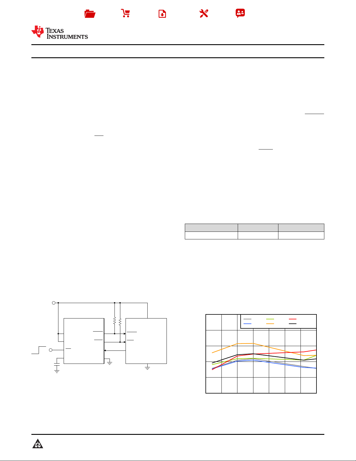
Typical Application Circuit
3 Description
The TPS3852 is a precision voltage supervisor with
an integrated window watchdog timer. The TPS3852
includes a precision undervoltage supervisor with an
undervoltage threshold (V
accuracy over the specified temperature range of
–40°C to +125°C. In addition, the TPS3852 includes
accurate hysteresis making the device ideal for use
with tight tolerance systems. The supervisor RESET
delay features a 15% accuracy, high-precision delay
timer.
The TPS3852 includes a programmable window
watchdog timer for a wide variety of applications. The
dedicated watchdog output (WDO) enables increased
resolution to help determine the nature of fault
conditions. The watchdog timeouts can be
programmed either by an external capacitor, or by
factory-programmed default delay settings. The
watchdog can be disabled to avoid undesired
watchdog timeouts during the development process.
The TPS3852 is available in a small 3.00-mm × 3.00mm, 8-pin VSON package.
Device Information
PART NUMBER PACKAGE BODY SIZE (NOM)
TPS3852 VSON (8) 3.00 mm × 3.00 mm
(1) For all available packages, see the orderable addendum at
the end of the data sheet.
Undervoltage Threshold (V
Temperature
) that achieves 0.8%
ITN
(1)
) Accuracy vs
ITN
1
An IMPORTANT NOTICE at the end of this data sheet addresses availability, warranty, changes, use in safety-critical applications,
intellectual property matters and other important disclaimers. PRODUCTION DATA.
TPS3852
SBVS302 –NOVEMBER 2016
www.ti.com
Table of Contents
1 Features.................................................................. 1
2 Applications ........................................................... 1
3 Description ............................................................. 1
4 Revision History..................................................... 2
5 Pin Configuration and Functions......................... 3
6 Specifications......................................................... 4
6.1 Absolute Maximum Ratings ...................................... 4
6.2 ESD Ratings.............................................................. 4
6.3 Recommended Operating Conditions....................... 4
6.4 Thermal Information.................................................. 5
6.5 Electrical Characteristics........................................... 5
6.6 Timing Requirements................................................ 6
6.7 Typical Characteristics.............................................. 8
7 Detailed Description............................................ 11
7.1 Overview ................................................................. 11
7.2 Functional Block Diagram....................................... 11
7.3 Feature Description................................................. 12
4 Revision History
DATE REVISION NOTES
November 2016 * Initial release.
7.4 Device Functional Modes........................................ 15
8 Application and Implementation ........................ 16
8.1 Application Information............................................ 16
8.2 Typical Application ................................................. 19
9 Power Supply Recommendations...................... 22
10 Layout................................................................... 22
10.1 Layout Guidelines ................................................. 22
10.2 Layout Example .................................................... 22
11 Device and Documentation Support ................. 23
11.1 Device Support...................................................... 23
11.2 Documentation Support ........................................ 23
11.3 Receiving Notification of Documentation Updates 23
11.4 Community Resources.......................................... 23
11.5 Trademarks........................................................... 23
11.6 Electrostatic Discharge Caution............................ 23
11.7 Glossary................................................................ 24
12 Mechanical, Packaging, and Orderable
Information........................................................... 24
2
Submit Documentation Feedback Copyright © 2016, Texas Instruments Incorporated
Product Folder Links: TPS3852
1VDD 8 RESET
2CWD 7 WDO
3MR 6 WDI
4GND 5 SET1
Not to scale
Thermal
Pad
www.ti.com
SBVS302 –NOVEMBER 2016
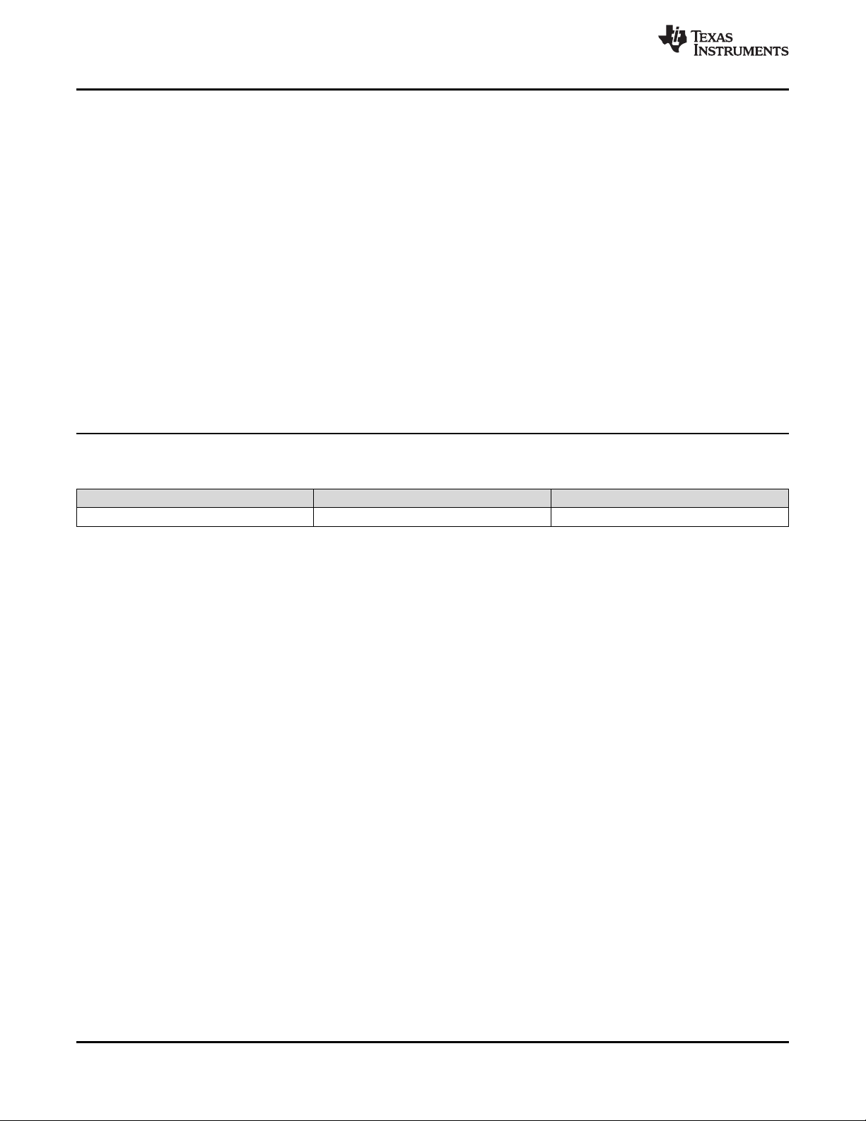
5 Pin Configuration and Functions
DRB Package
VSON-8 (8-Pins)
Top View
Pin Functions
NAME NO. I/O DESCRIPTION
Programmable watchdog timeout input. Watchdog timeout is set by connecting a capacitor between this pin and
CWD 2 —
GND 4 — Ground pin
MR 3 I
RESET 8 O
SET1 5 I Logic input. Grounding the SET1 pin disables the watchdog timer.
VDD 1 I Supply voltage pin. For noisy systems, connecting a 0.1-μF bypass capacitor is recommended.
WDI 6 I
WDO 7 O
Thermal pad — Connect the thermal pad to a large-area ground plane. The thermal pad is internally connected to GND.
ground. Furthermore, this pin can also be connected by a 10-kΩ resistor to VDD, or leaving unconnected (NC) further
enables the selection of the preset watchdog timeouts; see the Timing Requirements table.
When using a capacitor, the TPS3852 determines the window watchdog upper boundary with Equation 1. See
Table 3 and the CWD Functionality section for additional information.
Manual reset pin. A logical low on this pin issues a RESET. This pin is internally pulled up to VDD. RESET remains
low for a fixed reset delay (t
Reset output. Connect RESET using a 1-kΩ to 100-kΩ resistor to the desired pullup voltage rail (VPU). RESET goes
low when VDDgoes below the undervoltage threshold (V
RESET timeout-counter starts. At completion, RESET goes high. During startup, the state of RESET is undefined
below the specified power-on-reset (POR) voltage (V
monitored voltage is within the correct operating range (above V
Watchdog input. A falling transition (edge) must occur at this pin between the lower (t
window boundaries in order for WDO to not assert.
When the watchdog is not in use, the SET1 pin can be used to disable the watchdog. The input at WDI is ignored
when RESET or WDO are low (asserted) and also when the watchdog is disabled. If the watchdog is disabled, then
WDI cannot be left unconnected and must be driven to either VDD or GND.
Watchdog output. Connect WDO with a 1-kΩ to 100-kΩ resistor to the desired pullup voltage rail (VPU). WDO goes
low (asserts) when a watchdog timeout occurs. WDO only asserts when RESET is high. When a watchdog timeout
occurs, WDO goes low (asserts) for the set RESET timeout delay (t
impedance state.
) time after MR is deasserted (high).
RST
ITN
). Above POR, RESET goes low and remains low until the
POR
). When VDDis within the normal operating range, the
ITN+VHYST
) and the RESET timeout is complete.
) and upper (t
WDL(max)
). When RESET goes low, WDO is in a high-
RST
TPS3852
)
WDU(min)
Product Folder Links: TPS3852
Submit Documentation FeedbackCopyright © 2016, Texas Instruments Incorporated
3
TPS3852
SBVS302 –NOVEMBER 2016
www.ti.com
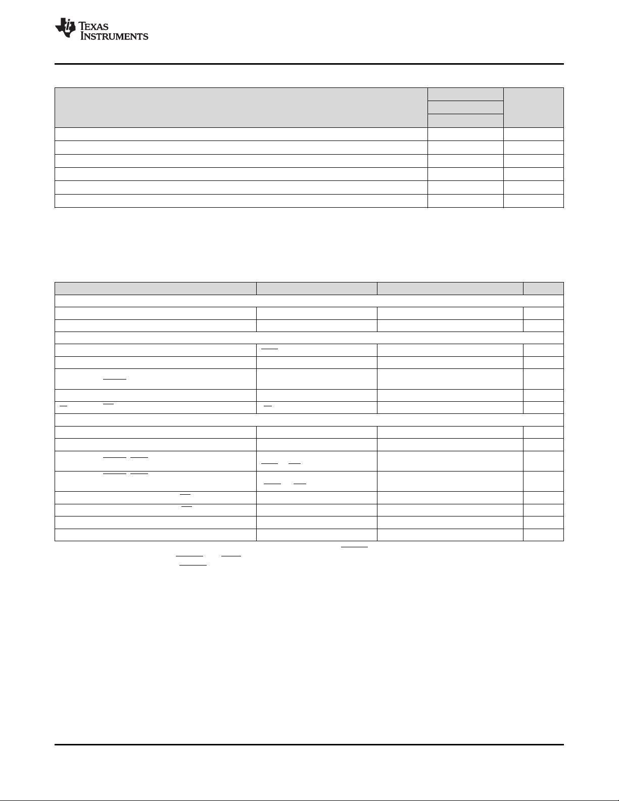
6 Specifications
6.1 Absolute Maximum Ratings
over operating free-air temperature range (unless otherwise noted)
Supply voltage range VDD –0.3 7 V
Output voltage range RESET, WDO –0.3 7 V
Voltage ranges
Output pin current ±20 mA
Input current (all pins) ±20 mA
Continuous total power dissipation See Thermal Information
Temperature
(1) Stresses beyond those listed under Absolute Maximum Ratings may cause permanent damage to the device. These are stress ratings
only, which do not imply functional operation of the device at these or any other conditions beyond those indicated under Recommended
Operating Conditions. Exposure to absolute-maximum-rated conditions for extended periods may affect device reliability.
(2) The absolute maximum rating is VDD+ 0.3 V or 7.0 V, whichever is smaller.
(3) Assume that TJ= TAas a result of the low dissipated power in this device.
SET1, WDI, MR –0.3 7 V
CWD, CRST –0.3 VDD+ 0.3
Operating junction, T
(3)
J
Operating free-air temperature, T
Storage, T
stg
(1)
MIN MAX UNIT
(2)
V
–40 150 °C
(3)
A
–40 150 °C
–65 150 °C
6.2 ESD Ratings
VALUE UNIT
(1)
±1000
±500
V
(ESD)
Electrostatic discharge
Human-body model (HBM), per ANSI/ESDA/JEDEC JS-001
Charged-device model (CDM), per JEDEC specification JESD22-
(2)
C101
(1) JEDEC document JEP155 states that 500-V HBM allows safe manufacturing with a standard ESD control process.
(2) JEDEC document JEP157 states that 250-V CDM allows safe manufacturing with a standard ESD control process.
6.3 Recommended Operating Conditions
over operating free-air temperature range (unless otherwise noted)
MIN NOM MAX UNIT
V
DD
V
SET1
V
MR
C
CWD
CWD Pull-up resistor to VDD 9 10 11 kΩ
R
PU
I
RESET
I
WDO
T
J
(1) Using a C
Supply pin voltage 1.6 6.5 V
SET1 pin voltage 0 6.5 V
MR pin voltage 0 6.5 V
Watchdog timing capacitor 0.1
(1)
1000
(1)
Pull-up resistor, RESET and WDO 1 10 100 kΩ
RESET pin current 10 mA
Watchdog output current 10 mA
Junction Temperature –40 125 °C
capacitor of 0.1 nF or 1000 nF gives a t
CWD
of 62.74 ms or 77.45 seconds, respectively.
WDU(typ)
V
nF
4
Submit Documentation Feedback Copyright © 2016, Texas Instruments Incorporated
Product Folder Links: TPS3852
TPS3852
www.ti.com
SBVS302 –NOVEMBER 2016
6.4 Thermal Information
TPS3852
THERMAL METRIC
(1)
UNITDRB (VSON)
8 PINS
R
θJA
R
θJC(top)
R
θJB
ψ
JT
ψ
JB
R
θJC(bot)
Junction-to-ambient thermal resistance 50.7 °C/W
Junction-to-case (top) thermal resistance 51.6 °C/W
Junction-to-board thermal resistance 25.8 °C/W
Junction-to-top characterization parameter 1.3 °C/W
Junction-to-board characterization parameter 25.8 °C/W
Junction-to-case (bottom) thermal resistance 7.1 °C/W
(1) For more information about traditional and new thermal metrics, see the Semiconductor and IC Package Thermal Metrics application
report.
6.5 Electrical Characteristics
At V
+ V
ITN
open-drain pull-up resistors are 10 kΩ for each output. Typical values are at TJ= 25°C.
GENERAL CHARACTERISTICS
(1)
V
DD
I
DD
RESET FUNCTION
(2)
V
POR
(3)
V
UVLO
V
ITN
V
HYST
I
MR
WINDOW WATCHDOG FUNCTION
I
CWD
V
CWD
V
OL
I
D
V
IL
V
IH
V
IL(WDI)
V
IH(WDI)
(1) During power on, VDDmust be a minimum 1.6 V for at least 300 µs before RESET correlates with VDD.
(2) When VDDfalls below V
(3) When VDDfalls below UVLO, RESET is driven low.
≤ VDD≤ 6.5 V over the operating temperature range of –40°C ≤ TA, TJ≤ 125°C, unless otherwise noted. The
HYST
PARAMETER TEST CONDITIONS MIN TYP MAX UNIT
Supply voltage 1.6 6.5 V
Supply Current 10 19 µA
Power-on reset voltage I
RESET
= 15 µA, V
= 0.25 V 0.8 V
OL(MAX)
Under Voltage Lock Out Voltage 1.35 V
Undervoltage threshold accuracy, entering
RESET
VDDfalling V
– 0.8% V
ITN
ITN
+ 0.8%
Hysteresis voltage VDDrising 0.2% 0.5% 0.8%
MR pin internal pull-up current VMR= 0 V 500 620 700 nA
CWD pin charge current CWD = 0.5 V 337 375 413 nA
CWD pin threshold voltage 1.192 1.21 1.228 V
RESET, WDO output low
RESET, WDO output leakage current, open-
drain
VDD = 5 V,
I
= I
RESET
VDD = V
V
= V
RESET
WDO
ITN
+ V
WDO
= 3 mA
HYST
= 6.5 V
0.4 V
,
1 µA
Low-level input voltage (MR, SET1) 0.25 V
High-level input voltage (MR, SET1) 0.8 V
Low-level input voltage (WDI) 0.3 × V
High-level input voltage (WDI) 0.8 × V
, RESET and WDO are undefined.
POR
DD
DD
V
V
Product Folder Links: TPS3852
Submit Documentation FeedbackCopyright © 2016, Texas Instruments Incorporated
5
VDD
RESET
WDI
WDO
t
RST
t
RST
t
RST
V
POR
V
ITN
t < t
WDU
t
WDL
< t < t
WDU
(1)
t < t
WDL
X
V
ITN
+ V
HYST
V
ITN
X
t
RST-DEL
t < t
WDU
TPS3852
SBVS302 –NOVEMBER 2016
6.6 Timing Requirements
At V
+ V
ITN
open-drain pull-up resistors are 10 kΩ for each output. Typical values are at TJ= 25°C.
t
INIT
RESET FUNCTION
t
RST
t
RST-DELVDD
t
MR-DEL
Watchdog Function
t
WDL
t
WDU
t
WD-
setup
t
WD-DEL
(1) SET1 = 0 means V
≤ VDD≤ 6.5 V over the operating temperature range of –40°C ≤ TA, TJ≤ 125°C, unless otherwise noted. The
HYST
MIN TYP MAX UNIT
CWD pin evaluation period 381 µs
Minimum MR, SET1 pin pulse duration 1 µs
Startup delay 300 µs
Reset timeout period 170 200 230 ms
to RESET delay
VDD= V
VDD= V
+ V
ITN
- 2.5% 17
ITN
+ 2.5% 35
HYST
MR to RESET delay 200 ns
(1)
(1)
680 800 920 ms
1.5 1.85 2.2 ms
(1)
(1)
1360 1600 1840 ms
9.3 11.0 12.7 ms
Window watchdog lower boundary
Window watchdog upper boundary
CWD = NC, SET1 = 0
CWD = NC, SET1 = 1
CWD = 10kΩ to VDD,
SET1 = 0
CWD = 10kΩ to VDD,
SET1 = 1
(1)
(1)
CWD = NC, SET1 = 0
CWD = NC, SET1 = 1
CWD = 10kΩ to VDD,
SET1 = 0
CWD = 10kΩ to VDD,
SET1 = 1
(1)
(1)
Setup time required for part to respond to changes on WDI after
being enabled
Minimum WDI pulse width 50 ns
WDI to WDO Delay 50 ns
< VIL, SET1 = 1 means V
SET1
SET1
> V
IH
www.ti.com
µs
Watchdog disabled
Watchdog disabled
Watchdog disabled
Watchdog disabled
150 µs
(1) See Figure 2 for WDI timing requirements.
6
Submit Documentation Feedback Copyright © 2016, Texas Instruments Incorporated
Figure 1. Timing Diagram
Product Folder Links: TPS3852

t
WDL(min)
Window
Timing
WDI
t
WDL(typ)
t
WDL(max)
t
WDU(min)
t
WDU(typ)
t
WDU(max)
WDO
= Tolerance Window
Early Fault
WDO
Late Fault
WDI
Valid
Window
Correct Operation
WDI
WDO
www.ti.com
TPS3852
SBVS302 –NOVEMBER 2016
Figure 2. TPS3852 Window Watchdog Timing
Product Folder Links: TPS3852
Submit Documentation FeedbackCopyright © 2016, Texas Instruments Incorporated
7
Temperature (qC)
Accuracy (%)
-50 -25 0 25 50 75 100 125
-0.5
-0.3
-0.1
0.1
0.3
0.5
Unit 1
Unit 2
Unit 3
Unit 4
Unit 5
Average
V
ITN
+ V
HYST
Accuracy (%)
Frequency (%)
0
5
10
15
20
25
30
35
40
45
-0.8 -0.6 -0.4 -0.2 0 0.2 0.4 0.6 0.8
Temperature (qC)
CWD Charging Current (nA)
-50 -25 0 25 50 75 100 125
364
368
372
376
380
1.6 V
6.5 V
Temperature (qC)
Accuracy (%)
-50 -25 0 25 50 75 100 125
-0.5
-0.3
-0.1
0.1
0.3
0.5
Unit 1
Unit 2
Unit 3
Unit 4
Unit 5
Average
VDD (V)
Supply Current (PA)
0 1 2 3 4 5 6 7
0
4
8
12
16
-40qC
0qC
25qC
105qC
125qC
Temperature (qC)
Manual Reset Threshold (V)
-50 -25 0 25 50 75 100 125
0.3
0.4
0.5
0.6
0.7
V
IL
V
IH
TPS3852
SBVS302 –NOVEMBER 2016
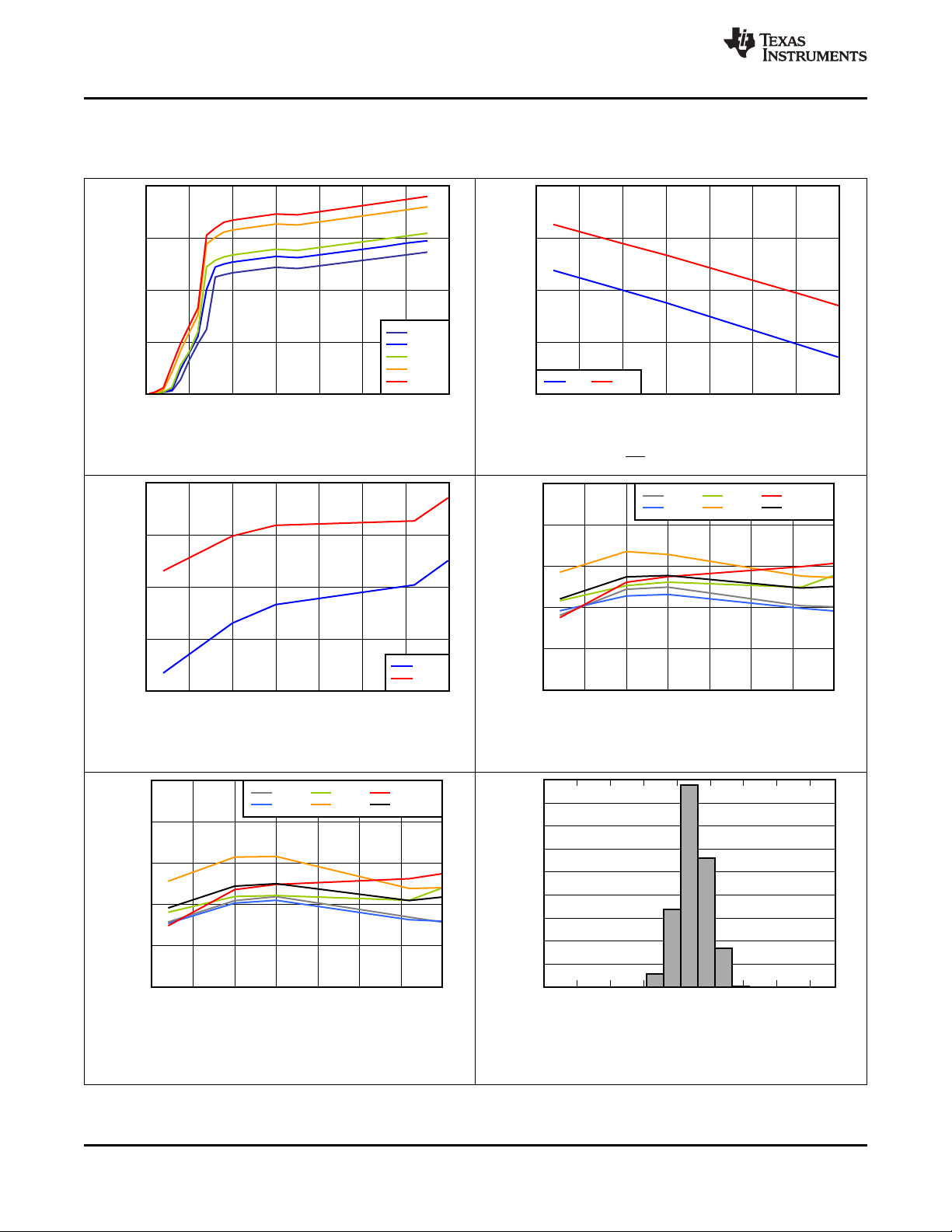
6.7 Typical Characteristics
All Typical Characteristics curves are taken at 25°C with, 1.6 V ≤ VDD ≤ 6.5 V unless other wise noted.
VDD = 1.6 V
www.ti.com
Figure 3. Supply Current vs V
DD
Figure 5. CWD Charging Current vs Temperature
TPS3852G33
Figure 6. V
Figure 4. MR Threshold vs Temperature
+ V
ITN
Accuracy vs Temperature
HYST
TPS3852G33
8
Figure 7. V
Accuracy vs Temperature
ITN
Submit Documentation Feedback Copyright © 2016, Texas Instruments Incorporated
Includes G and H versions; with 3.3-V nominal monitored voltage;
total units = 15,536
Product Folder Links: TPS3852
Figure 8. V
ITN
+ V
Accuracy Histogram
HYST

Overdrive (%)
Propagation Delay (Ps)
0 2 4 6 8 10
0
5
10
15
20
25
30
35
40
45
50
-40qC
0qC
25qC
105qC
125qC
Overdrive (%)
Propagation Delay (ms)
0 2 4 6 8 10
190
195
200
205
210
-40qC
0qC
25qC
105qC
125qC
I
RESET
(mA)
V
OL
(V)
0 1 2 3 4 5 6
0
0.2
0.4
0.6
0.8
1
1.2
1.4
1.6
-40qC
0qC
25qC
105qC
125qC
I
RESET
(mA)
V
OL
(V)
0 1 2 3 4 5 6
0
0.2
0.4
0.6
0.8
1
1.2
1.4
1.6
-40qC
0qC
25qC
105qC
125qC
V
ITN
Accuracy (%)
Frequency (%)
0
5
10
15
20
25
30
35
40
45
-0.8 -0.6 -0.4 -0.2 0 0.2 0.4 0.6 0.8
Hysteresis (%)
Frequency (%)
0
10
20
30
40
50
60
70
0.2 0.35 0.5 0.65 0.8
www.ti.com
Typical Characteristics (continued)
All Typical Characteristics curves are taken at 25°C with, 1.6 V ≤ VDD ≤ 6.5 V unless other wise noted.
TPS3852
SBVS302 –NOVEMBER 2016
Includes G and H versions; with 3.3-V nominal monitored voltage;
total units = 15,536
Figure 9. V
Accuracy Histogram
ITN
VDD = 1.6 V
Figure 11. Low-Level RESET Voltage vs RESET Current
Includes G and H versions; with 3.3-V nominal monitored voltage;
total units = 15,536
Figure 10. Hysteresis Histogram
VDD = 6.5 V
Figure 12. Low-Level RESET Voltage vs RESET Current
TPS3852G33 entering undervoltage
Figure 13. Propagation Delay vs Overdrive
TPS3852G33 exiting undervoltage
Figure 14. Propagation Delay (t
Product Folder Links: TPS3852
) vs Overdrive
RST
Submit Documentation FeedbackCopyright © 2016, Texas Instruments Incorporated
9
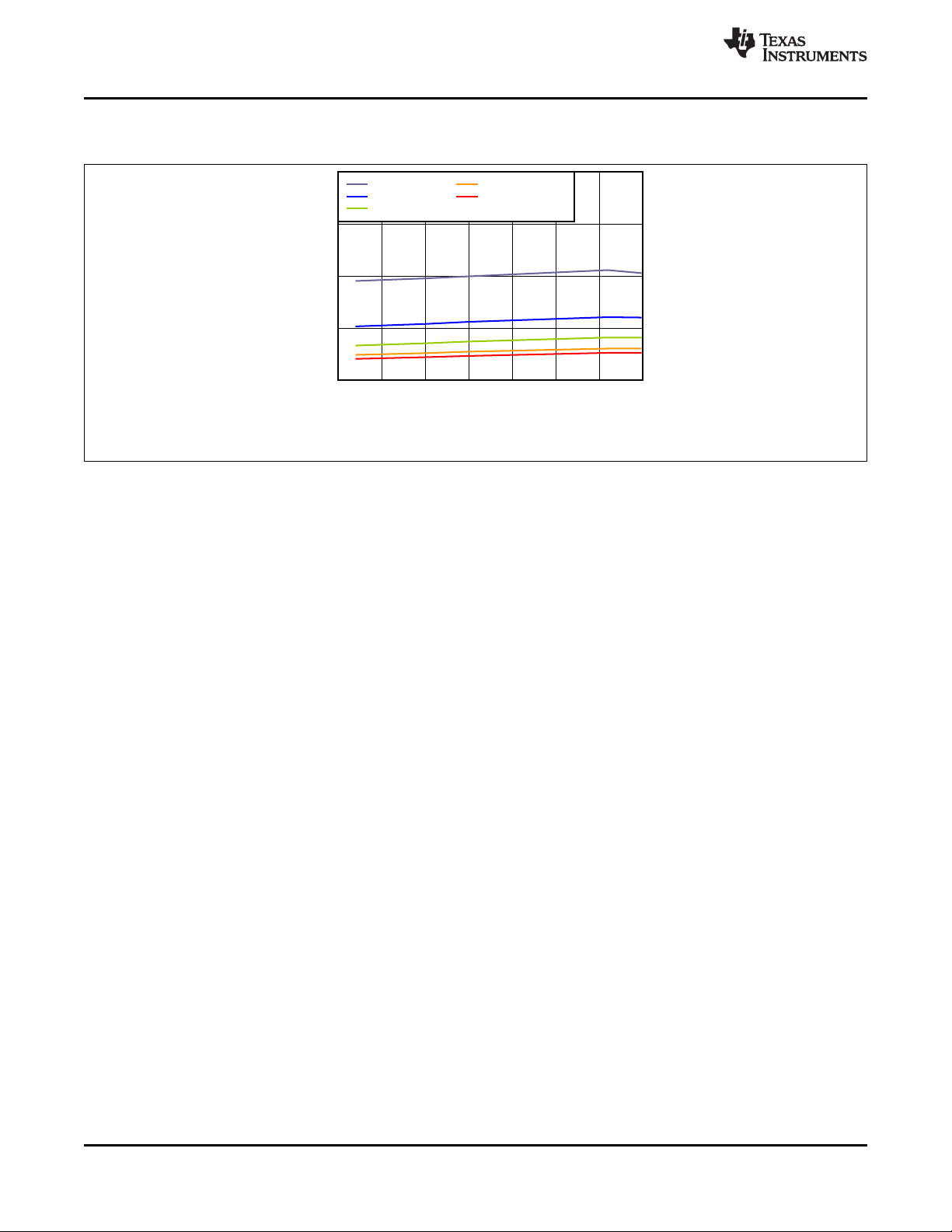
Temperature (qC)
Glitch Immunity (Ps)
-50 -25 0 25 50 75 100 125
5
10
15
20
25
Overdrive = 3%
Overdrive = 5%
Overdrive = 7%
Overdrive = 9%
Overdrive = 10%
TPS3852
SBVS302 –NOVEMBER 2016
Typical Characteristics (continued)
All Typical Characteristics curves are taken at 25°C with, 1.6 V ≤ VDD ≤ 6.5 V unless other wise noted.
V
= 3.168 V
ITN
Figure 15. High to Low Glitch Immunity vs Temperature
www.ti.com
10
Submit Documentation Feedback Copyright © 2016, Texas Instruments Incorporated
Product Folder Links: TPS3852
 Loading...