

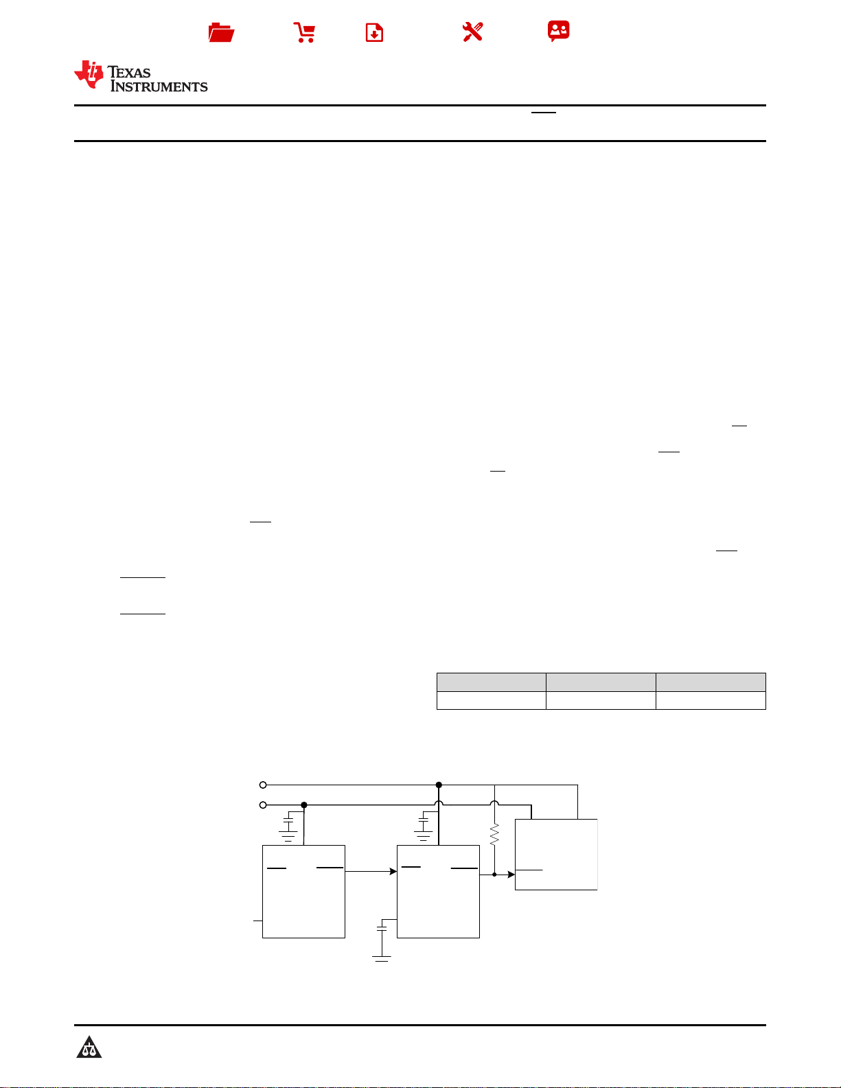
TPS3840PL18
MR
VDD
GNDCT
RESET
TPS3840DL30
VDD
GND
RESET
MR
CT
Microcontroller
V
CORE
V
I/O
3.3V
1.8V
RESET
Product
Folder
Order
Now
Technical
Documents
Tools &
Software
Support &
Community
TPS3840-Q1
SNVSBA1B –APRIL 2019–REVISED APRIL 2020
TPS3840-Q1 Automotive Nano IQVoltage Supervisor With MR and Programmable Delay
1 Features
1
• Qualified for automotive applications
• AEC-Q100 qualified with the following results:
– Device temperature grade 1: –40°C to +125°C
ambient operating temperature
– Device HBM ESD classification level 2
– Device CDM ESD classification level C7B
• Wide operating voltage : 1.5 V to 10 V
– Use external resistors to extend Vin range
• Nano supply current : 350 nA (Typ), 700 nA (Max)
• Fixed threshold voltage (V
– Threshold from 1.6 V to 4.9 V in 0.1-V steps
– High accuracy: 1% (Typ), 1.5% (Max)
– Built-in hysteresis (V
– 1.6 V < V
– 3.1 V ≤ V
• Fast start-up delay (t
≤ 3.0 V = 100 mV (typical)
IT-
< 4.9 V = 200 mV (typical)
IT-
STRT
• Programmable capacitor-based reset time delay:
– tD: 50 µs (no capacitor) to 6.2 s (10-µF)
• Active-low manual reset (MR)
• Three output topologies:
– TPS3840DL-Q1: open-drain, active-low
(RESET)
– TPS3840PL-Q1: push-pull, active-low
(RESET)
– TPS3840PH-Q1: push-pull, active-high
(RESET)
• Package: 5-pin SOT-23 (DBV)
)
IT-
)
IT+
): 350 µs (Max)
2 Applications
• Automotive head unit and cluster
• Automotive display, integrated cockpit and driver
monitoring
• Telematics control unit and emergency call
3 Description
The TPS3840-Q1 family of voltage supervisors or
reset ICs can operate at high voltage levels while
maintaining very low quiescent current across the
whole VDDand temperature range. TPS3840-Q1
offers best combination of low power consumption,
high accuracy and low propagation delay (t
µs typical).
Reset output signal is asserted when the voltage at
VDD drops below the negative voltage threshold (V
or when manual reset is pulled to a low logic (V
Reset signal is cleared when VDDrise above V
hysteresis (V
above V
) and manual reset (MR) is floating or
IT+
and the reset time delay (tD) expires.
MR_H
Reset time delay can be programmed by connecting
a capacitor between CT pin and ground. For a fast
reset CT pin can be left floating.
Additional features: Low power-on reset voltage
(V
), built-in glitch immunity protection for MR and
POR
VDD, built-in hysteresis, low open-drain output
leakage current (I
). TPS3840-Q1 is a perfect
LKG(OD)
voltage monitoring solution for automotive
applications and battery-powered / low power
applications.
Device Information
PART NUMBER PACKAGE BODY SIZE (NOM)
TPS3840-Q1 SOT-23 (5) (DBV) 2.90 mm × 1.60 mm
(1) For package details, see the mechanical drawing addendum
at the end of the data sheet.
(1)
p_HL
IT-
= 30
IT-
MR_L
plus
)
).
Typical Application Circuit
1
An IMPORTANT NOTICE at the end of this data sheet addresses availability, warranty, changes, use in safety-critical applications,
intellectual property matters and other important disclaimers. PRODUCTION DATA.

TPS3840-Q1
SNVSBA1B –APRIL 2019–REVISED APRIL 2020
www.ti.com
Table of Contents
1 Features.................................................................. 1
2 Applications ........................................................... 1
3 Description ............................................................. 1
4 Revision History..................................................... 2
5 Device Comparison ............................................... 3
6 Pin Configuration and Functions......................... 4
7 Specifications......................................................... 5
7.1 Absolute Maximum Ratings ...................................... 5
7.2 ESD Ratings ............................................................ 5
7.3 Recommended Operating Conditions....................... 5
7.4 Thermal Information.................................................. 5
7.5 Electrical Characteristics........................................... 6
7.6 Timing Requirements................................................ 7
7.7 Typical Characteristics.............................................. 9
8 Detailed Description............................................ 16
8.1 Overview................................................................. 16
8.2 Functional Block Diagram ....................................... 16
8.3 Feature Description................................................. 16
8.4 Device Functional Modes........................................ 19
9 Application and Implementation ........................ 20
9.1 Application Information............................................ 20
9.2 Typical Application ................................................. 20
10 Power Supply Recommendations ..................... 25
11 Layout................................................................... 25
11.1 Layout Guidelines ................................................. 25
11.2 Layout Example .................................................... 25
12 Device and Documentation Support ................. 26
12.1 Device Nomenclature............................................ 26
12.2 Receiving Notification of Documentation Updates 27
12.3 Community Resources.......................................... 27
12.4 Trademarks........................................................... 27
12.5 Electrostatic Discharge Caution............................ 27
12.6 Glossary................................................................ 27
13 Mechanical, Packaging, and Orderable
Information........................................................... 27
4 Revision History
NOTE: Page numbers for previous revisions may differ from page numbers in the current version.
Changes from Revision A (September 2019) to Revision B Page
• Changed equation 5 and 6 ................................................................................................................................................... 17
• Added section describing further details on capacitor. ........................................................................................................ 18
• Deleted non-relevant application design. ............................................................................................................................ 22
Changes from Original (April 2019) to Revision A Page
• Advance Information to Production Data Release ................................................................................................................ 1
2
Submit Documentation Feedback Copyright © 2019–2020, Texas Instruments Incorporated
Product Folder Links: TPS3840-Q1
TPS3840 XX XX XXX Q1
OUTPUT TYPE
DL: Open-Drain Active-Low
PL: Push-Pull Active-Low
PH: Push-Pull Active-High
Threshold Voltage
16: 1.6V
17: 1.7V
...
49: 4.9V
See Device
Threshold Table
Package
DBV: SOT-23
TPS3840-Q1
www.ti.com
SNVSBA1B –APRIL 2019–REVISED APRIL 2020
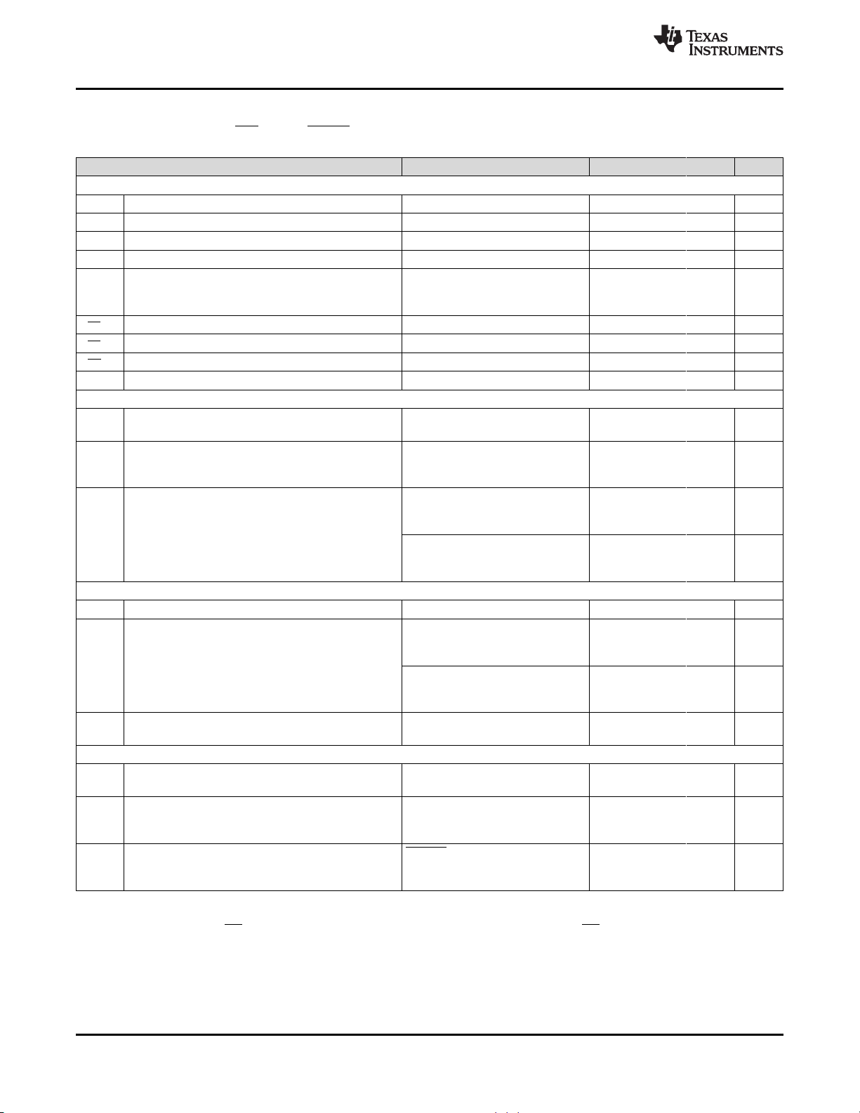
5 Device Comparison
Figure 1 shows the device nomenclature to determine the device variant. Other voltages from Table 3 at the end
of datasheet can be sampled upon request, please contact TI sales representative for details.
Figure 1. Device Nomenclature
Product Folder Links: TPS3840-Q1
Submit Documentation FeedbackCopyright © 2019–2020, Texas Instruments Incorporated
3
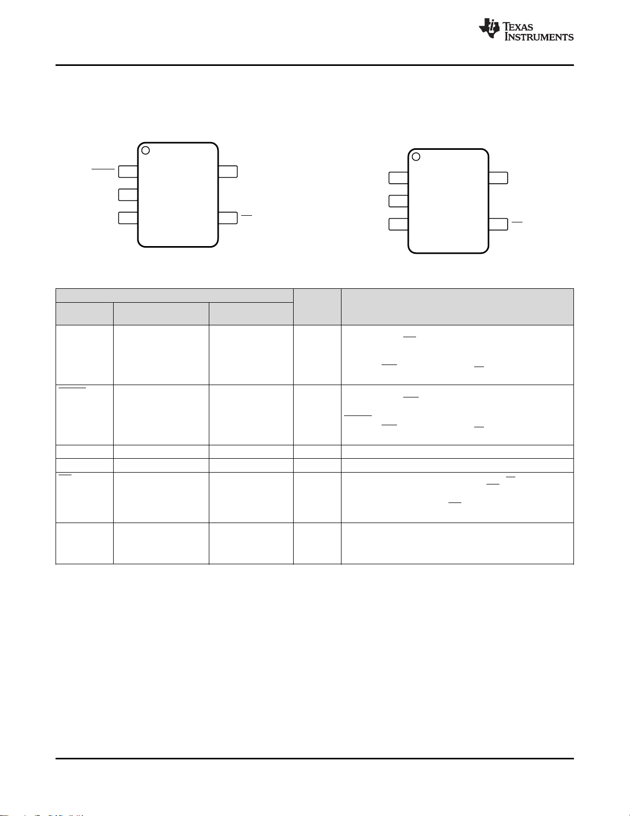
1RESET
2VDD
3GND 4 MR
5 CT
Not to scale
/ NC
1RESET
2VDD
3GND 4 MR
5 CT
Not to scale
/ NC
TPS3840-Q1
SNVSBA1B –APRIL 2019–REVISED APRIL 2020
6 Pin Configuration and Functions
www.ti.com
DBV Package
5-Pin
TPS3840PL-Q1, TPS3840DL-Q1 Top View
DBV Package
5-Pin
TPS3840PH-Q1 Top View
Pin Functions
PIN
NAME TPS3840PL-Q1,
TPS3840PH-Q1
TPS3840DL-Q1
RESET N/A 1 O Active-High Output Reset Signal: This pin is driven high
RESET 1 N/A O Active-Low Output Reset Signal: This pin is driven logic
VDD 2 2 I Input Supply Voltage. TPS3840-Q1 monitors VDD voltage
GND 3 3 _ Ground
MR / NC 4 4 I Manual Reset. Pull this pin to a logic low (V
CT 5 5 - Capacitor Time Delay Pin. The CT pin offers a user-
I/O DESCRIPTION
when either the MR pin is driven to a logic low or VDD
voltage falls below the negative voltage threshold (V
RESET remains high (asserted) for the delay time period (tD)
after both MR is floating or above V
rise above V
IT+.
MR_L
when either the MR pin is driven to a logic low or VDD
voltage falls below the negative voltage threshold (V
RESET remains low (asserted) for the delay time period (tD)
after both MR is floating or above V
rise above V
IT+.
MR_L
reset signal in the output pin. After the MR pin is left floating
or pull to V
reset delay time(tD) expires. MR can be left floating when
the output goes to the nominal state after the
MR_H
not in use. NC stands for "No Connection" or floating.
programmable delay time. Connect an external capacitor on
this pin to adjust time delay. When not in use leave pin
floating for the smallest fixed time delay.
).
IT-
and VDD voltage
).
IT-
and VDD voltage
) to assert a
MR_L
4
Submit Documentation Feedback Copyright © 2019–2020, Texas Instruments Incorporated
Product Folder Links: TPS3840-Q1
TPS3840-Q1
www.ti.com
SNVSBA1B –APRIL 2019–REVISED APRIL 2020
7 Specifications
7.1 Absolute Maximum Ratings
over operating free-air temperature range, unless otherwise noted
VDD –0.3 12
RESET (TPS3840PL) –0.3 VDD+ 0.3
Voltage
RESET (TPS3840PH) –0.3 VDD+ 0.3
RESET (TPS3840DL) –0.3 12
(2)
MR
CT –0.3 5.5
Current RESET pin and RESET pin ±70 mA
Temperature
(3)
Operating junction temperature, T
Storage, T
stg
(1) Stresses beyond those listed under Absolute Maximum Rating may cause permanent damage to the device. These are stress ratings
only, which do not imply functional operation of the device at these or any other conditions beyond those indicated under Recommended
Operating Condition. Exposure to absolute-maximum-rated conditions for extended periods may affect device reliability.
(2) If the logic signal driving MR is less than VDD, then additional current flows into VDDand out of MR. VMRshould not be higher than V
(3) As a result of the low dissipated power in this device, it is assumed that TJ= TA.
7.2 ESD Ratings
Human body model (HBM), per ANSI/ESDA/JEDEC JS-
(1)
V
(ESD)
Electrostatic discharge
(1) JEDEC document JEP155 states that 500-V HBM allows safe manufacturing with a standard ESD control process.
(2) JEDEC document JEP157 states that 250-V CDM allows safe manufacturing with a standard ESD control process.
001
Charged device model (CDM), per JEDEC specification
JESD22-C101
(2)
(1)
MIN MAX UNIT
V
–0.3 12
J
–40 150
–65 150
°C
VALUE UNIT
± 2000
V
± 750
DD.
7.3 Recommended Operating Conditions
over operating free-air temperature range (unless otherwise noted)
MIN NOM MAX UNIT
V
DD
V
, V
RESET
RESET
I
, I
RESET
RESET
T
J
(1)
V
MR
(1) If the logic signal driving MR is less than VDD, then additional current flows into VDDand out of MR. VMRshould not be higher than V
Input supply voltage 1.5 10 V
RESET pin and RESET pin voltage 0 10 V
RESET pin and RESET pin current 0 ±5 mA
Junction temperature (free air temperature) –40 125 °C
Manual reset pin voltage 0 V
DD
V
7.4 Thermal Information
TPS3840
THERMAL METRIC
R
θJA
R
θJC(top)
R
θJB
ψ
JT
ψ
JB
R
θJC(bot)
Junction-to-ambient thermal resistance 187.5 °C/W
Junction-to-case (top) thermal resistance 109.2 °C/W
Junction-to-board thermal resistance 92.8 °C/W
Junction-to-top characterization parameter 35.4 °C/W
Junction-to-board characterization parameter 92.5 °C/W
Junction-to-case (bottom) thermal resistance N/A °C/W
(1) For more information about traditional and new thermal metrics, see the Semiconductor and IC Package Thermal Metrics application
report.
(1)
UNITDBV (SOT23-5)
5 PINS
DD.
Product Folder Links: TPS3840-Q1
Submit Documentation FeedbackCopyright © 2019–2020, Texas Instruments Incorporated
5
TPS3840-Q1
SNVSBA1B –APRIL 2019–REVISED APRIL 2020
www.ti.com
7.5 Electrical Characteristics
At 1.5 V ≤ VDD≤ 10 V, CT = MR = Open, RESET pull-up resistor (R
and over the operating free-air temperature range – 40°C to 125°C, unless otherwise noted. Typical values are at TJ= 25°C.
PARAMETER TEST CONDITIONS MIN TYP MAX UNIT
COMMON PARAMETERS
V
V
V
V
I
DD
V
V
R
R
TPS3840PL (Push-Pull Active-Low)
V
V
V
TPS3840PH (Push-Pull Active-High)
V
V
V
TPS3840DL(Open-Drain)
V
V
I
lkg(OD)
(1) V
(2) V
(3) If the logic signal driving MR is less than VDD, then additional current flows into VDD and out of MR
(4) V
Input supply voltage 1.5 10 V
DD
Negative-going input threshold accuracy
ITHYS
HYS
Hysteresis on V
Hysteresis on V
pin V
IT-
pin V
IT-
(1)
-40°C to 125°C –1.5 1 1.5 %
= 3.1 V to 4.9 V 175 200 225 mV
IT-
= 1.6 V to 3.0 V 75 100 125 mV
IT-
VDD = 1.5 V < VDD< 10 V
Supply current into VDD pin
VDD > V
TA= -40°C to 125°C
Manual reset logic low input
MR_L
Manual reset logic high input
MR_H
Manual reset internal pull-up resistance 100 kΩ
MR
CT pin internal resistance 350 500 650 kΩ
CT
Power on Reset Voltage
POR
Low level output voltage
OL
(3)
(3)
V
(4)
OL(max)
I
OUT(Sink)
1.5 V < VDD< 5 V
VDD< V
I
OUT(Sink)
1.5 V < VDD< 5 V
VDD> V
High level output voltage
OH
I
OUT(Source
5 V < VDD< 10 V
VDD> V
I
OUT(Source)
Power on Reset Voltage
POR
(4)
VOH, I
OUT(Source)
1.5 V < VDD< 5 V
VDD> V
Low level output voltage
OL
I
OUT(Sink)
1.5 V < VDD< 5 V
VDD> V
I
OUT(Sink)
High level output voltage 1.5 V < VDD< 5 V, VDD< V
OH
Power on Reset Voltage
POR
Low level output voltage
OL
(4)
I
OUT(Source)
V
OL(max)
I
OUT (Sink)
1.5 V < VDD< 5 V
VDD< V
I
OUT(Sink)
RESET pin in High Impedance,
Open-Drain output leakage current
threshold voltage range from 1.6 V to 4.9 V in 100 mV steps, for released versions see Device Voltage Thresholds table.
IT-
= V
IT+
POR
+ V
HYS
IT-
is the minimum VDDvoltage level for a controlled output state. VDDslew rate ≤ 100mV/µs
VDD= V
V
< V
IT+
) = 100 kΩ to VDD, output reset load (C
pull-up
(2)
IT+
0.7V
DD
= 200 mV
= 200 nA
IT-
= 2 mA
IT+
(2)
0.8V
DD
) = 2 mA
IT+
(2)
0.8V
DD
= 5 mA
= 500 nA 950 mV
(2)
IT+
= 2 mA
(2)
IT+
= 5 mA
,
= 2 mA
IT-
0.8V
DD
= 0.2 V
= 5.6 uA
IT-
= 2 mA
= 5.5 V
RESET
DD
) = 10 pF
LOAD
300 700 nA
600 mV
300 mV
200 mV
200 mV
200 mV
950 mV
200 mV
90 nA
V
V
V
V
6
Submit Documentation Feedback Copyright © 2019–2020, Texas Instruments Incorporated
Product Folder Links: TPS3840-Q1
t
D
t
P_HL
VDD
V
POR
V
OH
V
OL
V
IT+
V
DD(MIN)
V
IT-
RESET
t
STRT + tD
t
P_HL
t
STRT + tD
TPS3840-Q1
www.ti.com
SNVSBA1B –APRIL 2019–REVISED APRIL 2020
7.6 Timing Requirements
At 1.5 V ≤ VDD≤ 10 V, CT = MR = Open, RESET pull-up resistor (R
and over the operating free-air temperature range – 40°C to 125°C, VDD slew rate < 100mV / us, unless otherwise noted.
Typical values are at TJ= 25°C.
PARAMETER TEST CONDITIONS MIN TYP MAX UNIT
t
STRT
t
P_HL
t
D
t
GI_VIT-
t
MR_PW
t
MR_RES
t
MR_tD
Startup Delay
Propagation detect delay for VDD falling
below V
Reset time delay
Glitch immunity V
MR pin pulse duration to initiate reset 300 ns
Propagation delay from MR low to reset VDD= 4.5 V, MR < V
Delay from release MR to deasert reset
(1) When VDD starts from less than the specified minimum VDDand then exceeds V
capacitor at CT pin will add tDdelay to t
(2) t
(3) The MIN and MAX reset time delay with external capacitor depends on RCTand is calculated using Equation 5 and Equation 6 in
measured from threhold trip point (V
P_HL
Section 8.3.2
(4) Overdrive % = [(VDD/ V
(1)
IT-
CT pin open 100 220 350 µs
VDD= V
IT+
to (V
CT pin = open
(3)
CT pin = 10 nF 6.2 ms
CT pin = 1 µF 619 ms
5% V
IT-
overdrive
IT-
VDD= 4.5 V,
MR = V
MR_L
time
STRT
) to VOLfor active low variants and VOHfor active high variants.
IT-
) - 1] × 100%
IT-
) = 100 kΩ to VDD, output reset load (C
pull-up
(2)
) - 10%
IT-
(4)
MR_L
to V
MR_H
, reset is release after the startup delay (t
IT+
) = 10 pF
LOAD
15 30 µs
50 µs
10 µs
700 ns
t
D
STRT
ms
), a
(1) t
D (no cap)
is included in t
time delay. If tDdelay is programmed by an external capacitor connected to CT pin then
STRT
tDprogrammed time will be added to the startup time, VDD slew rate = 100 mV / µs.
(2) Open-Drain timing diagram assumes pull-up resistor is connected to RESET
Figure 4. Timing Diagram TPS3840DL-Q1 (Open-Drain Active-Low)
Product Folder Links: TPS3840-Q1
Submit Documentation FeedbackCopyright © 2019–2020, Texas Instruments Incorporated
7
t
D
t
P_HL
VDD
V
POR
V
OH
V
OL
V
IT+
V
DD(MIN)
V
IT-
RESET
t
STRT + tD
t
P_HL
t
STRT + tD
t
D
t
P_HL
VDD
V
POR
V
OH
V
OL
V
IT+
V
DD(MIN)
V
IT-
RESET
t
P_HL
t
STRT + tD
t
STRT + tD
TPS3840-Q1
SNVSBA1B –APRIL 2019–REVISED APRIL 2020
www.ti.com
(3) t
D (no cap)
is included in t
time delay. If tDdelay is programmed by an external capacitor connected to CT pin, then
STRT
tDprogrammed time will be added to the startup time. VDD slew rate = 100 mV / µs.
Figure 5. Timing Diagram TPS3840PL-Q1 (Push-Pull Active-Low)
(4) t
D (no cap)
tDprogrammed time will be added to the total startup time. VDD slew rate = 100 mV / µs.
is included in t
time delay. If tDdelay is programmed by an external capacitor connected to CT pin, then
STRT
Figure 6. Timing Diagram TPS3840PH-Q1 (Push-Pull Active-High)
8
Submit Documentation Feedback Copyright © 2019–2020, Texas Instruments Incorporated
Product Folder Links: TPS3840-Q1
Temperature (°C)
VIT- Accuracy (%)
-40 -20 0 20 40 60 80 100 120 140
-0.6
-0.5
-0.4
-0.3
-0.2
-0.1
0
0.1
0.2
0.3
0.4
0.5
0.6
VIT_
PL16
PL28
PL49
Temperature (°C)
VIT- Accuracy (%)
-40 -20 0 20 40 60 80 100 120 140
-0.6
-0.5
-0.4
-0.3
-0.2
-0.1
0
0.1
0.2
0.3
0.4
0.5
0.6
VIT_
PH16
PH30
PH49
VDD (V)
IDD (µA)
1 2 3 4 5 6 7 8 9 10
0.05
0.1
0.15
0.2
0.25
0.3
0.35
0.4
0.45
0.5
0.55
0.6
25°C
-40°C
125°C
Temperature (°C)
VIT- Accuracy (%)
-40 -20 0 20 40 60 80 100 120 140
-0.6
-0.5
-0.4
-0.3
-0.2
-0.1
0
0.1
0.2
0.3
0.4
0.5
0.6
VIT_
DL16
DL29
DL49
VDD (V)
IDD (µA)
1 2 3 4 5 6 7 8 9 10
0.05
0.1
0.15
0.2
0.25
0.3
0.35
0.4
0.45
0.5
0.55
0.6
25°C
-40°C
125°C
VDD (V)
IDD (µA)
1 2 3 4 5 6 7 8 9 10
0.05
0.1
0.15
0.2
0.25
0.3
0.35
0.4
0.45
0.5
0.55
0.6
25°C
-40°C
125°C
TPS3840-Q1
www.ti.com
SNVSBA1B –APRIL 2019–REVISED APRIL 2020
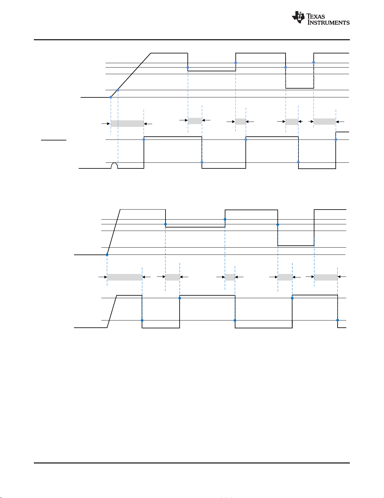
7.7 Typical Characteristics
Typical characteristics show the typical performance of the TPS3840-Q1 device. Test conditions are TJ= 25°C, VDD= 3.3 V,
R
pull-up
= 100 kΩ, C
= 50 pF, unless otherwise noted.
Load
Figure 7. Supply Current vs Supply Voltage for
TPS3840DL49-Q1
Figure 9. Supply Current vs Supply Voltage for
TPS3840PH49-Q1
Figure 8. Supply Current vs Supply Voltage for
TPS3840PL49-Q1
Figure 10. Negative-going Input Threshold Accuracy over
Temperature for TPS3840DL-Q1
Figure 11. Negative-going Input Threshold Accuracy over
Temperature for TPS3840PL-Q1
Product Folder Links: TPS3840-Q1
Figure 12. Negative-going Input Threshold Accuracy over
Temperature for TPS3840PH-Q1
Submit Documentation FeedbackCopyright © 2019–2020, Texas Instruments Incorporated
9
VDD (V)
V
RESET
(V)
0 1 2 3 4 5 6 7 8 9 10
-1
0
1
2
3
4
5
6
7
8
9
10
VRES
25°C
-40°C
125°C
VDD (V)
V
RESET
(V)
0 1 2 3 4 5 6 7 8 9 10
0
0.5
1
1.5
2
2.5
3
3.5
4
4.5
5
5.5
VRES
25°C
-40°C
125°C
VDD (V)
V
RESET
(V)
0 1 2 3 4 5 6 7 8 9 10
-1
0
1
2
3
4
5
6
7
8
9
10
VRES
25°C
-40°C
125°C
Temperature (°C)
VHYS Accuracy (%)
-40 -20 0 20 40 60 80 100 120 140
-20
-15
-10
-5
0
5
10
15
20
Vhys
PH16
PH30
PH49
Temperature (°C)
VHYS Accuracy (%)
-40 -20 0 20 40 60 80 100 120 140
-20
-15
-10
-5
0
5
10
15
20
Vhys
DL16
DL29
DL49
Temperature (°C)
VHYS Accuracy (%)
-40 -20 0 20 40 60 80 100 120 140
-20
-15
-10
-5
0
5
10
15
20
Vhys
PL16
PL28
PL49
TPS3840-Q1
SNVSBA1B –APRIL 2019–REVISED APRIL 2020
www.ti.com
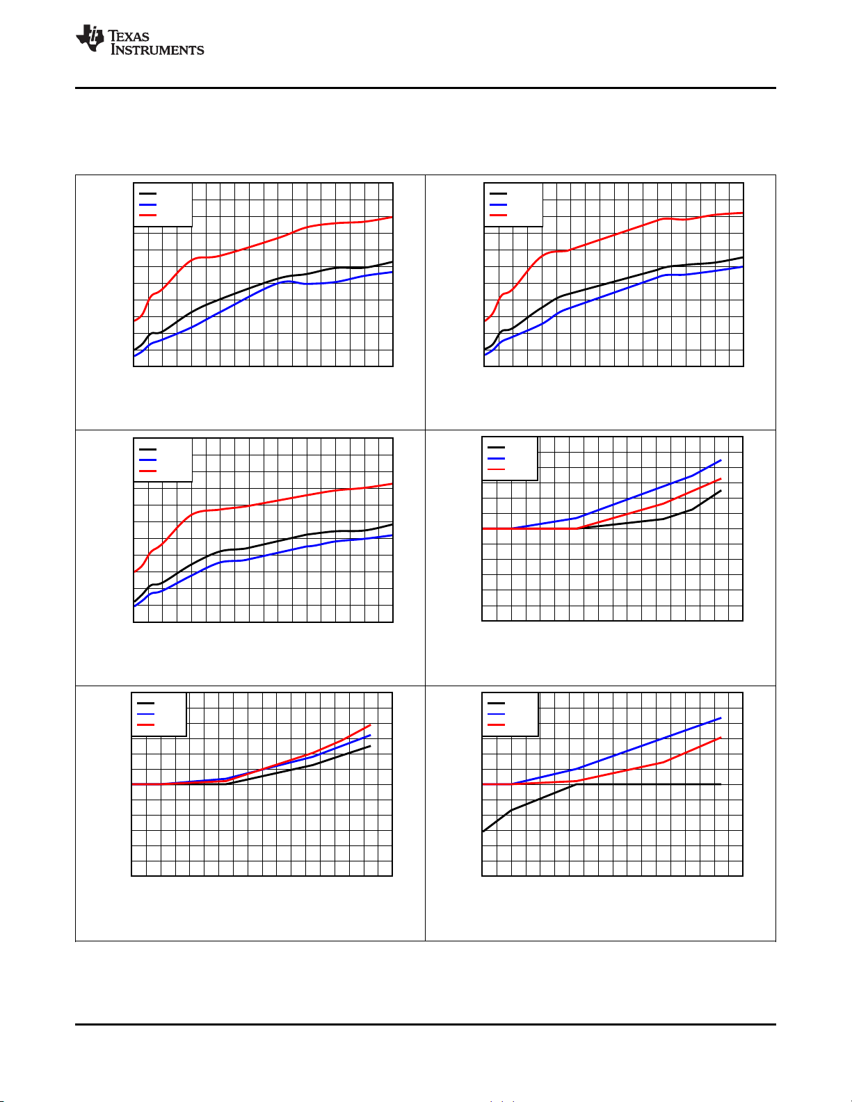
Typical Characteristics (continued)
Typical characteristics show the typical performance of the TPS3840-Q1 device. Test conditions are TJ= 25°C, VDD= 3.3 V,
R
pull-up
= 100 kΩ, C
= 50 pF, unless otherwise noted.
Load
Figure 13. Input Threshold V
TPS3840DL-Q1
Figure 15. Input Threshold V
TPS3840PH-Q1
Hysteresis Accuracy for
IT-
Hysteresis Accuracy for
IT-
Figure 14. Input Threshold V
Hysteresis Accuracy for
IT-
TPS3840PL-Q1
Figure 16. Output Voltage vs Input Voltage for
TPS3840DL49-Q1
10
Figure 17. Output Voltage vs Input Voltage for
TPS3840PL49-Q1
Submit Documentation Feedback Copyright © 2019–2020, Texas Instruments Incorporated
Figure 18. Output Voltage vs Input Voltage for
TPS3840PH49-Q1
Product Folder Links: TPS3840-Q1
I
RESET
(mA)
V
OL
(V)
0 0.5 1 1.5 2 2.5 3 3.5 4 4.5 5
0
10
20
30
40
50
60
70
80
VOL_
25°C
-40°C
125°C
VDD (V)
VOL (V)
5 5.5 6 6.5 7 7.5 8 8.5 9 9.5 10 10.5
0.015
0.02
0.025
0.03
0.035
0.04
0.045
0.05
0.055
0.06
0.065
0.07
0.075
0.08
0.085
0.09
VOLv
25°C
-40°C
125°C
I
RESET
(mA)
V
OL
(V)
0 0.5 1 1.5 2 2.5 3 3.5 4 4.5 5
-20
0
20
40
60
80
100
120
140
VOL_
25°C
-40°C
125°C
VDD (V)
VOL (V)
1.5 2 2.5 3 3.5 4 4.5 5
0.015
0.02
0.025
0.03
0.035
0.04
0.045
0.05
0.055
VOLv
25°C
-40°C
125°C
I
RESET
(mA)
V
OL
(V)
0 0.5 1 1.5 2 2.5 3 3.5 4 4.5 5
0
20
40
60
80
100
120
140
VOL_
25°C
-40°C
125°C
VDD (V)
VOL (V)
1.5 2 2.5 3 3.5 4 4.5 5
0.015
0.02
0.025
0.03
0.035
0.04
0.045
0.05
0.055
VOLv
25°C
-40°C
125°C
TPS3840-Q1
www.ti.com
SNVSBA1B –APRIL 2019–REVISED APRIL 2020
Typical Characteristics (continued)
Typical characteristics show the typical performance of the TPS3840-Q1 device. Test conditions are TJ= 25°C, VDD= 3.3 V,
R
pull-up
= 100 kΩ, C
= 50 pF, unless otherwise noted.
Load
Figure 19. Low Level Output Voltage vs I
TPS3840DL49-Q1
Figure 21. Low Level Output Voltage vs I
TPS3840PL49-Q1
RESET
RESET
for
for
Figure 20. Low Level Output Voltage vs VDDfor
TPS3840DL49-Q1
Figure 22. Low Level Output Voltage vs VDD for
TPS3840PL49-Q1
Figure 23. Low Level Output Voltage vs I
TPS3840PH49-Q1
for
RESET
Product Folder Links: TPS3840-Q1
Figure 24. Low Level Output Voltage vs VDD for
TPS3840PH49-Q1
Submit Documentation FeedbackCopyright © 2019–2020, Texas Instruments Incorporated
11

Temperature (°C)
V_MR_L (V)
-40 -20 0 20 40 60 80 100 120 140
0.5
0.75
1
1.25
1.5
1.75
2
2.25
2.5
2.75
MR_L
DL16
DL29
DL49
Temperature (°C)
V_MR_L (V)
-40 -20 0 20 40 60 80 100 120 140
0.5
0.75
1
1.25
1.5
1.75
2
2.25
2.5
2.75
MR_L
PL16
PL28
PL49
I
RESET
(mA)
V
OH
(V)
0 0.5 1 1.5 2 2.5 3 3.5 4 4.5 5
1.25
1.3
1.35
1.4
1.45
1.5
1.55
1.6
VOH_
25°C
-40°C
125°C
VDD (V)
VOH (V)
1.5 2 2.5 3 3.5 4 4.5 5
1
1.5
2
2.5
3
3.5
4
4.5
5
VOHv
25°C
-40°C
125°C
I
RESET
(mA)
V
OH
(V)
0 0.5 1 1.5 2 2.5 3 3.5 4 4.5 5
9.75
9.775
9.8
9.825
9.85
9.875
9.9
9.925
9.95
9.975
10
VOH_
25°C
-40°C
125°C
VDD (V)
VOH (V)
1.5 2 2.5 3 3.5 4 4.5 5
1
1.5
2
2.5
3
3.5
4
4.5
5
VOHv
25°C
-40°C
125°C
TPS3840-Q1
SNVSBA1B –APRIL 2019–REVISED APRIL 2020
www.ti.com
Typical Characteristics (continued)
Typical characteristics show the typical performance of the TPS3840-Q1 device. Test conditions are TJ= 25°C, VDD= 3.3 V,
R
pull-up
= 100 kΩ, C
= 50 pF, unless otherwise noted.
Load
Figure 25. High Level Output Voltage vs I
TPS3840PL49-Q1
Figure 27. High Level Output Voltage vs I
TPS3840PH49-Q1
RESET
RESET
for
for
Figure 26. High Level Output Voltage over Temperature for
TPS3840PL49-Q1
Figure 28. High Level Output Voltage Over Temperature for
TPS3840PH49-Q1
Figure 29. Manual Reset Logic Low Voltage Threshold Over
12
Submit Documentation Feedback Copyright © 2019–2020, Texas Instruments Incorporated
Temperature for TPS3840DL-Q1
Figure 30. Manual Reset Logic Low Voltage Threshold Over
Temperature for TPS3840PL-Q1
Product Folder Links: TPS3840-Q1

Overdrive (%)
Glitch Immunity (µs)
5 10 15 20 25 30 35 40 45 50
12
13
14
15
16
17
18
19
20
21
22
Glit
25°C
-40°C
125°C
Temperature (°C)
R_CT (kohm)
-40 -20 0 20 40 60 80 100 120 140
458
460
462
464
466
468
470
472
474
476
478
RCTv
DL49
PL49
PH49
Temperature (°C)
V_MR_H (V)
-40 -20 0 20 40 60 80 100 120 140
0.75
1
1.25
1.5
1.75
2
2.25
2.5
2.75
MR_H
PL16
PL28
PL49
Temperature (°C)
V_MR_H (V)
-40 -20 0 20 40 60 80 100 120 140
0.75
1
1.25
1.5
1.75
2
2.25
2.5
2.75
MR_H
PH16
PH30
PH49
Temperature (°C)
V_MR_L (V)
-40 -20 0 20 40 60 80 100 120 140
0.5
0.75
1
1.25
1.5
1.75
2
2.25
2.5
2.75
MR_L
PH16
PH230
PH49
Temperature (°C)
V_MR_H (V)
-40 -20 0 20 40 60 80 100 120 140
0.75
1
1.25
1.5
1.75
2
2.25
2.5
2.75
MR_H
DL16
DL29
DL49
TPS3840-Q1
www.ti.com
SNVSBA1B –APRIL 2019–REVISED APRIL 2020
Typical Characteristics (continued)
Typical characteristics show the typical performance of the TPS3840-Q1 device. Test conditions are TJ= 25°C, VDD= 3.3 V,
R
pull-up
= 100 kΩ, C
= 50 pF, unless otherwise noted.
Load
Figure 31. Manual Reset Logic Low Voltage Threshold Over
Temperature for TPS3840PH-Q1
Figure 33. Manual Reset Logic High Voltage Threshold Over
Temperature for TPS3840PL-Q1
Figure 32. Manual Reset Logic High Voltage Threshold Over
Temperature for TPS3840DL-Q1
Figure 34. Manual Reset Logic High Voltage Threshold Over
Temperature for TPS3840PH-Q1
Figure 35. Glitch Immunity on V
with TPS3840PL28-Q1)
vs Overdrive (Data Taken
IT-
Product Folder Links: TPS3840-Q1
Figure 36. CT Pin Internal Resistance Over Temperature
Submit Documentation FeedbackCopyright © 2019–2020, Texas Instruments Incorporated
13

Capacitor Value (µF)
tD with Capacitor (s)
1 2 3 4 5 6 7 8 9 10
0.5
1
1.5
2
2.5
3
3.5
4
4.5
5
Dela
25°C
-40°C
125°C
Temperature (°C)
t_P_HL (µs)
-40 -20 0 20 40 60 80 100 120 140
14.75
15
15.25
15.5
15.75
16
16.25
16.5
16.75
17
17.25
DL49
PL49
PH49
Capacitor (µF)
t_D (ms)
0.01 0.02 0.05 0.1 0.2 0.3 0.5 1 2 3 4 5 67 10
0
500
1000
1500
2000
2500
3000
3500
4000
4500
5000
Dela
25°C
-40°C
125°C
Capacitor Value (µF)
tD with Capacitor (ms)
0.01 0.02 0.03 0.050.07 0.1 0.2 0.3 0.5 0.7 1
0
100
200
300
400
500
600
Dela
25°C
-40°C
125°C
Temperature (°C)
t_STRT (µs)
-40 -20 0 20 40 60 80 100 120 140
170
175
180
185
190
195
200
205
210
215
Star
DL49
PL49
PH49
Temperature (°C)
t_D no Capacitor (µs)
-40 -20 0 20 40 60 80 100 120 140
3
6
9
12
15
Dela
DL49
PL49
PH49
TPS3840-Q1
SNVSBA1B –APRIL 2019–REVISED APRIL 2020
www.ti.com
Typical Characteristics (continued)
Typical characteristics show the typical performance of the TPS3840-Q1 device. Test conditions are TJ= 25°C, VDD= 3.3 V,
R
pull-up
= 100 kΩ, C
Figure 37. Startup Delay Over Temperature Figure 38. Reset Time Delay with No Capacitor Over
= 50 pF, unless otherwise noted.
Load
Temperature
Figure 39. Reset Time Delay vs Capacitor Value (Data Taken
with TPS3840PL16-Q1)
14
Figure 41. Reset Time Delay vs Large Capacitor Values
(Data Taken with TPS3840PL16-Q1)
Submit Documentation Feedback Copyright © 2019–2020, Texas Instruments Incorporated
Product Folder Links: TPS3840-Q1
Figure 40. Reset Time Delay vs Small Capacitor Values
(Data Taken with TPS3840PL16-Q1)
Figure 42. Propagation Detect Time Delay for VDD Falling
Below V
(High-to-Low) Over Temperature
IT-

Temperature (°C)
T_MR_RES (ns)
-40 -20 0 20 40 60 80 100 120 140
415
420
425
430
435
440
445
450
455
460
465
MR_r
DL49
PL49
PH49
Temperature (°C)
t_MR_ tD (µs)
-40 -20 0 20 40 60 80 100 120 140
3.1
3.15
3.2
3.25
3.3
3.35
3.4
3.45
3.5
3.55
MRde
DL49
PL49
PH49
TPS3840-Q1
www.ti.com
SNVSBA1B –APRIL 2019–REVISED APRIL 2020
Typical Characteristics (continued)
Typical characteristics show the typical performance of the TPS3840-Q1 device. Test conditions are TJ= 25°C, VDD= 3.3 V,
R
pull-up
= 100 kΩ, C
= 50 pF, unless otherwise noted.
Load
Figure 43. Propagation Time Delay from MR Asserted to
Reset Over Temperature
Figure 44. Propagation Time Delay from MR Release to
Deasserted Reset Over Temperature
Product Folder Links: TPS3840-Q1
Submit Documentation FeedbackCopyright © 2019–2020, Texas Instruments Incorporated
15

+
±
V
REF
VDD
RESET
RESET
GND
VDD
CT / NC
MR / NC
R
MR
Copyright © 2019, Texas Instruments Incorporated
R
CT
Subreg
Voltage
Divider
VDD
VDD
GND
Push-Pull variants
TPS3840-Q1
SNVSBA1B –APRIL 2019–REVISED APRIL 2020
www.ti.com
8 Detailed Description
8.1 Overview
The TPS3840-Q1 is a family of wide VDD and nano-quiescent current voltage detectors with fixed threshold
voltage. TPS3840-Q1 features include programable reset time delay using external capacitor, active-low manual
reset, 1% typical monitor threshold accuracy with hysteresis and glitch immunity.
Fixed negative threshold voltages (V
TPS3840-Q1 is available in SOT-23 5 pin industry standard package.
8.2 Functional Block Diagram
) can be factory set from 1.6 V to 4.9 V (see Table 3 for available options).
IT-
8.3 Feature Description
8.3.1 Input Voltage (VDD)
VDD pin is monitored by the internal comparator to indicate when VDD falls below the fixed threshold voltage.
VDD also functions as the supply for the internal bandgap, internal regulator, state machine, buffers and other
control logic blocks. Good design practice involve placing a 0.1 uF to 1 uF bypass capacitor at VDD input for
noisy applications to ensure enough charge is available for the device to power up correctly.
16
Submit Documentation Feedback Copyright © 2019–2020, Texas Instruments Incorporated
Product Folder Links: TPS3840-Q1

Overdrive
Pulse
Duration
VDD
V
IT-
V
IT+
Hystersis Width
V
IT+
V
IT-
RESET
RESET
Hystersis Width
V
IT+
V
IT-
TPS3840-Q1
www.ti.com
SNVSBA1B –APRIL 2019–REVISED APRIL 2020
Feature Description (continued)
8.3.1.1 VDD Hysteresis
The internal comparator has built-in hysteresis to avoid erroneous output reset release. If the voltage at the VDD
pin falls below V
(V
) the output reset is deasserted after tDdelay.
HYS
8.3.1.2 VDD Transient Immunity
The TPS3840-Q1 is immune to quick voltage transients or excursion on VDD. Sensitivity to transients depends
on both pulse duration and overdrive. Overdrive is defined by how much VDD deviates from the specified
threshold. Threshold overdrive is calculated as a percent of the threshold in question, as shown in Equation 1.
Overdrive = | (VDD/ V
the output reset is asserted. When the voltage at the VDD pin goes above V
IT-
Figure 45. Hysteresis Diagram
– 1) × 100% | (1)
IT-
plus hysteresis
IT-
Figure 46. Overdrive vs Pulse Duration
8.3.2 User-Programmable Reset Time Delay
The reset time delay can be set to a minimum value of 50 µs by leaving the CT pin floating, or a maximum value
of approximately 6.2 seconds by connecting 10 µF delay capacitor. The reset time delay (tD) can be programmed
by connecting a capacitor no larger than 10 µF between CT pin and GND.
The relationship between external capacitor (C
) in F at CT pin and the time delay (tD) in seconds is given
CT_EXT
by Equation 2.
tD= -ln (0.29) x RCTx C
Equation 2 is simplified to Equation 3 by plugging RCTand t
tD= 618937 x C
+ 50 µs (3)
CT_EXT
Equation 4 solves for external capacitor value (C
C
= (tD- 50 µs) ÷ 618937 (4)
CT_EXT
+ tD(no cap) (2)
CT_EXT
D(no cap)
) in units of F where tDis in units of seconds
CT_EXT
given in Electrical Characteristics section:
The reset delay varies according to three variables: the external capacitor variance (CCT), CT pin internal
resistance (RCT) provided in the Electrical Characteristics table, and a constant. The minimum and maximum
variance due to the constant is shown in Equation 5 and Equation 6.
s t
D (minimum)
t
D (maximum)
= -ln (0.36) x R
= -ln (0.26) x R
CT (min)
CT (max)
x C
x C
CT (min)
CT (max)
+ t
D (no cap, min)
+ t
D (no cap, max)
Product Folder Links: TPS3840-Q1
(5)
(6)
Submit Documentation FeedbackCopyright © 2019–2020, Texas Instruments Incorporated
17

V
IT+
t
P_HL
V
HYS
t
D
V
IT+
V
HYS
V
IT-
t
MR_tD
V
MR_L
t
MR_RES
t
MR_PW
Reset not asserted
Pulse width less than t
MR_PW
RESET
MR
VDD
V
MR_H
V
IT-
TPS3840-Q1
SNVSBA1B –APRIL 2019–REVISED APRIL 2020
www.ti.com
Feature Description (continued)
The recommended maximum delay capacitor for the TPS3840 is limited to 10 µF as this ensures there is enough
time for the capacitor to fully discharge when the reset condition occurs. When a voltage fault occurs, the
previously charged up capacitor discharges, and if the monitored voltage returns from the fault condition before
the delay capacitor discharges completely, the delay capacitor will begin charging from a voltage above zero and
the reset delay will be shorter than expected. Larger delay capacitors can be used so long as the capacitor has
enough time to fully discharge during the duration of the voltage fault.
8.3.3 Manual Reset (MR) Input
The manual reset (MR) input allows a processor GPIO or other logic circuits to initiate a reset. A logic low on MR
with pulse duration longer than t
and VDD is above V
, reset is deasserted after the user programmed reset time delay (tD) expires.
IT+
MR_RES
If MR is not controlled externally, then MR can be left disconnected. If the logic signal controlling MR is less than
VDD, then additional current flows from VDD into MR internally. For minimum current consumption, drive MR to
either VDD or GND. VMRmust not be higher than VDD voltage.
will causes reset output to assert. After MR returns to a logic high (V
MR_H
)
Figure 47. Timing Diagram MR and RESET (TPS3840DL-Q1)
8.3.4 Output Logic
8.3.4.1 RESET Output, Active-Low
RESET (Active-Low) applies to TPS3840DL-Q1 (Open-Drain) and TPS3840PL-Q1 (Push-Pull) hence the "L" in
the device name. RESET remains high (deasserted) as long as VDD is above the negative threshold (V
the MR pin is floating or above V
. If VDD falls below the negative threshold (V
MR_H
) or if MR is driven low, then
IT-
RESET is asserted.
When MR is again logic high or floating and VDD rise above V
, the delay circuit will hold RESET low for the
IT+
specified reset time delay (tD). When the reset time delay has elapsed, the RESET pin goes back to logic high
voltage (VOH).
The TPS3840DL-Q1 (Open-Drain) version, denoted with "D" in the device name, requires a pull-up resistor to
hold RESET pin high. Connect the pull-up resistor to the desired pull-up voltage source and RESET can be
pulled up to any voltage up to 10 V independent of the VDD voltage. To ensure proper voltage levels, give some
consideration when choosing the pull-up resistor values. The pull-up resistor value determines the actual VOL, the
output capacitive loading, and the output leakage current (I
The Push-Pull variants (TPS3840PL and TPS3840PH), denoted with "P" in the device name, does not require a
).
LKG(OD)
pull-up resistor.
18
Submit Documentation Feedback Copyright © 2019–2020, Texas Instruments Incorporated
Product Folder Links: TPS3840-Q1
IT-
) and

TPS3840-Q1
www.ti.com
SNVSBA1B –APRIL 2019–REVISED APRIL 2020
Feature Description (continued)
8.3.4.2 RESET Output, Active-High
RESET (active-high), denoted with no bar above the pin label, applies only to TPS3840PH-Q1 push-pull activehigh version. RESET remains low (deasserted) as long as VDD is above the threshold (V
reset signal (MR) is logic high or floating. If VDD falls below the negative threshold (V
IT-
) and the manual
IT-
) or if MR is driven low,
then RESET is asserted driving the RESET pin to high voltage (VOH).
When MR is again logic high and VDD is above V
the delay circuit will hold RESET high for the specified reset
IT+
time delay (tD). When the reset time delay has elapsed, the RESET pin goes back to low voltage (VOL).
8.4 Device Functional Modes
Table 1 summarizes the various functional modes of the device. Logic high is represented by "H" and logic low is
represented by "L".
Table 1. Truth Table
VDD MR RESET RESET
VDD < V
V
POR
(1) When VDDfalls below V
< VDD< V
VDD ≥ V
VDD ≥ V
VDD ≥ V
POR
ITITIT-
(1)
IT-
, undervoltage-lockout (UVLO) takes effect and output reset is held asserted until VDDfalls below V
DD(MIN)
Ignored Undefined Undefined
Ignored H L
L H L
H L H
Floating L H
POR
.
8.4.1 Normal Operation (VDD> V
When VDD is greater than V
the trip point (V
) and the logic state of MR.
IT-
DD(min)
)
DD(min)
, the reset signal is determined by the voltage on the VDD pin with respect to
• MR high: the reset signal corresponds to VDD with respect to the threshold voltage.
• MR low: in this mode, the reset is asserted regardless of the threshold voltage.
8.4.2 VDD Between VPOR and V
When the voltage on VDD is less than the V
DD(min)
DD(min)
voltage, and greater than the power-on-reset voltage (V
the reset signal is asserted.
8.4.3 Below Power-On-Reset (VDD< V
When the voltage on VDD is lower than V
)
POR
, the device does not have enough bias voltage to internally pull the
POR
asserted output low or high and reset voltage level is undefined.
POR
),
Product Folder Links: TPS3840-Q1
Submit Documentation FeedbackCopyright © 2019–2020, Texas Instruments Incorporated
19

TPS3840PL30
MR
VDD
GNDCT
RESET
TPS3840DL16
VDD
GND
RESET
MR
CT
Microcontroller
V
CORE
3.3V
RESET
VDD
LDO
EN
1.8 V
0.047µF
VI/O
NC
1 µF 1 µF
10NŸ
TPS3840-Q1
SNVSBA1B –APRIL 2019–REVISED APRIL 2020
www.ti.com
9 Application and Implementation
NOTE
Information in the following applications sections is not part of the TI component
specification, and TI does not warrant its accuracy or completeness. TI’s customers are
responsible for determining suitability of components for their purposes. Customers should
validate and test their design implementation to confirm system functionality.
9.1 Application Information
The following sections describe in detail how to properly use this device, depending on the requirements of the
final application.
9.2 Typical Application
9.2.1 Design 1: Dual Rail Monitoring with Power-Up Sequencing
A typical application for the TPS3840-Q1 is voltage rail monitoring and power-up sequencing as shown in
Figure 48. The TPS3840-Q1 can be used to monitor any rail above 1.6 V. In this design application, two
TPS3840-Q1 devices monitor two separate voltage rails and sequences the rails upon power-up. The
TPS3840PL30-Q1 is used to monitor the 3.3-V main power rail and the TPS3840DL16-Q1 is used to monitor the
1.8-V rail provided by the LDO for other system peripherals. The RESET output of the TPS3840PL30-Q1 is
connected to the ENABLE input of the LDO. A reset event is initiated on either voltage supervisor when the VDD
voltage is less than V
or when MR is driven low by an external source.
IT-
9.2.1.1 Design Requirements
This design requires voltage supervision on two separate rails: 3.3-V and 1.8-V rails. The voltage rail needs to
sequence upon power up with the 3.3-V rail coming up first followed by the 1.8-V rail at least 25 ms after.
Two Rail Voltage Supervision Monitor 3.3-V and 1.8-V rails
Voltage Rail Sequencing
Output logic voltage 3.3-V Open-Drain 3.3-V Open-Drain
Maximum device current
consumption
20
Figure 48. TPS3840-Q1 Voltage Rail Monitor and Power-Up Sequencer Design Block Diagram
PARAMETER DESIGN REQUIREMENT DESIGN RESULT
Submit Documentation Feedback Copyright © 2019–2020, Texas Instruments Incorporated
Two TPS3840-Q1 devices provide voltage monitoring with 1%
accuracy with device options available in 0.1 V variations
Power up the 3.3-V rail first followed
by 1.8-V rail 25 ms after
1 µA Each TPS3840-Q1 requires 350 nA typical
Product Folder Links: TPS3840-Q1
The CT capacitor on TPS38240PL28 is set to 0.047 µF for a
reset time delay of 29 ms typical

VDD
RESET
(LDO Enable)
V (LDO)
OUT
30ms delay from VDD (3.3V) to LDO Enable set by 0.047µF on CT of TPS3840PL30
Negligible delay from LDO Enable to 1.8V V
OUT
TPS3840-Q1
www.ti.com
SNVSBA1B –APRIL 2019–REVISED APRIL 2020
9.2.1.2 Detailed Design Procedure
The primary constraint for this application is choosing the correct device to monitor the supply voltage of the
microprocessor. The TPS3840-Q1 can monitor any voltage between 1.6 V and 10 V and is available in 0.1 V
increments. Depending on how far away from the nominal voltage rail the user wants the voltage supervisor to
trigger determines the correct voltage supervisor variant to choose. In this example, the first TPS3840-Q1
triggers when the 3.3-V rail falls to 3.0 V. The second TPS3840-Q1 triggers a reset when the 1.8-V rail falls to
1.6 V. The secondary constraint for this application is the reset time delay that must be at least 25 ms to allow
the microprocessor, and all other devices using the 3.3-V rail, enough time to startup correctly before the 1.8-V
rail is enabled via the LDO. Because a minimum time is required, the user must account for capacitor tolerance.
For applications with ambient temperatures ranging from –40°C to +125°C, CCTcan be calculated using RCTand
solving for CCTin Equation 2. Solving Equation 2 for 25 ms gives a minimum capacitor value of 0.04 µF which is
rounded up to a standard value 0.047 µF to account for capacitor tolerance.
A 1-µF decoupling capacitor is connected to the VDD pin as a good analog design practice. The pull-up resistor
is only required for the Open-Drain device variants and is calculated to maintain the RESET current within the ±5
mA limit found in the Recommended Operating Conditions: R
Pull-up
= V
÷ 5 mA. For this design, a standard
Pull-up
10-kΩ pull-up resistor is selected to minimize current draw when RESET is asserted. Keep in mind the lower the
pull-up resistor, the higher VOL. The MR pin can be connected to an external signal if desired or left floating if not
used due to the internal pull-up resistor to VDD.
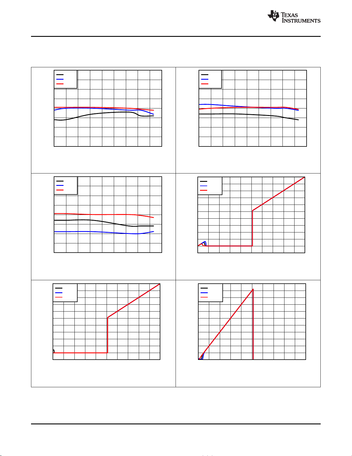
9.2.1.3 Application Curves
Figure 49. Startup Sequence Highlighting the Delay Between 3.3V and 1.8V Rails
Submit Documentation FeedbackCopyright © 2019–2020, Texas Instruments Incorporated
Product Folder Links: TPS3840-Q1
21

TPS3840-Q1
SNVSBA1B –APRIL 2019–REVISED APRIL 2020
www.ti.com
9.2.2 Design 2: Automotive Off-Battery Monitoring
The initial power stage in automotive applications starts with the 12 V battery. Variation of the battery voltage is
common between 9 V and 16 V. Furthermore, If cold-cranking and load dump conditions are considered, voltage
transients can occur as low as 3 V and as high as 42V. In this design example, we are highlighting the ability for
low power , direct off-battery voltage supervision. Figure 50 illustrates an example of how the TPS3840-Q1 is
monitoring the battery voltage while being powered by it as well. For more information, read this application
report on how to achieve nano-amp IQvoltage supervision in automotive, wide-vin applications.
Figure 50. Fast Start Undervoltage Supervisor with Level-Shifted Input
22
Submit Documentation Feedback Copyright © 2019–2020, Texas Instruments Incorporated
Product Folder Links: TPS3840-Q1

TPS3840-Q1
www.ti.com
SNVSBA1B –APRIL 2019–REVISED APRIL 2020
9.2.2.1 Design Requirements
This design requires voltage supervision on a 12-V power supply voltage rail with possibility of the 12-V rail rising
up as high as 42 V. The undervoltage fault occurs when the power supply voltage drops below 7.7 V.
PARAMETER DESIGN REQUIREMENT DESIGN RESULT
Power Rail Voltage Supervision
Maximum Input Power Operate with power supply input up to 42 V.
Output logic voltage Open-Drain Output Topology
Maximum system current
consumption
Voltage Monitor Accuracy Typical voltage monitor accuracy of 2.5%.
Delay when returning from fault
condition
Monitor 12-V power supply for undervoltage
condition, trigger a undervoltage fault at 7.7 V.
35 uA when power supply is at 12 V typical
RESET delay of at least 200 ms when returning
from a undervoltage fault.
TPS3840-Q1 provides voltage monitoring with 1%
accuracy with device options available in 0.1 V
variations. Resistor dividers are calculated based
on device variant and desired threshold voltage.
The TPS3840-Q1 limits VDD to 10 V but can
monitor voltages higher than the maximum VDD
voltage with the use of an external resistor divider.
Due to large variance in battery voltage, an opendrain output is recommended to provide the correct
reset signal.
TPS3840-Q1 requires 350 nA (typical) and the
external resistor divider will also consume current.
There is a tradeoff between current consumption
and voltage monitor accuracy but generally set the
resistor divider to consume 100 times current into
VDD.
The TPS3840-Q1 has 1% typical voltage monitor
accuracy. By decreasing the ratio of resistor
values, the resistor divider will consume more
current but the accuracy will increase. The resistor
tolerance also needs to be accounted for.
CCT= 0.33 µF sets 204 ms delay
9.2.2.2 Detailed Design Procedure
The primary constraint for this application is monitoring a 12-V rail while preventing the VDD pin on TPS3840-Q1
from exceeding the recommended maximum of 10 V. This is accomplished by sizing the resistor divider so that
when the 12-V rail drops to 7.7 V, the VDD pin for TPS3840-Q1 will be at 1.6 V which is the V
threshold for
IT-
triggering a undervoltage condition for TPS3840DL16-Q1 as shown in Equation 7. Reasonably sized resistors
were selected for the voltage divider. While selecting lower resistor values may increase current, this allows for
additional accuracy from the resistor divider.
V
rail_trigger
where V
TPS3840, and R1and R2are the top and bottom resistors of the external resistor divider. V
= V
rail_trigger
x (R2÷ (R1+ R2)) (7)
IT-
is the trigger voltage of the rail being monitored, V
is the falling threshold on the VDD pin of
IT-
is fixed per device
IT-
variant and is 1.6 V for TPS3840DL16-Q1. Substituting in the values from Figure 50, the undervoltage trigger
threshold for the rail is set to 7.7 V. Given that R1= 100 kΩ, R2= 26.2 kΩ.
Because the undervoltage trigger of 10 V on the rail corresponds to 1.6 V undervoltage threshold trigger of the
TPS3840-Q1 device, there is room for the rail to rise up while maintaining less than 10 V on the VDD pin of the
TPS3840-Q1. Equation 8 shows the maximum rail voltage that still meets the 10 V maximum at the VDD pin for
TPS3840-Q1.
V
= 10 V x (26.2 kΩ ÷ (100 kΩ + 26.2 kΩ)) = 48.168 V (8)
rail_max
This means the monitored voltage rail can go as high as 48.168 V and not violate the recommended maximum
for the VDD pin on TPS3840-Q1. This is useful when monitoring a voltage rail that has a wide range that may go
much higher than the nominal rail voltage such as in this case. Notice that the resistor values chosen are less
than 100kΩ to preserve the accuracy set by the internal resistor divider. Good design practice recommends using
a 0.1-µF capacitor on the VDD pin and this capacitance may need to increase when using an external resistor
divider.
Product Folder Links: TPS3840-Q1
Submit Documentation FeedbackCopyright © 2019–2020, Texas Instruments Incorporated
23

TPS3840-Q1
SNVSBA1B –APRIL 2019–REVISED APRIL 2020
www.ti.com
9.2.2.3 Application Curves: TPS3840EVM
These application curves are taken with the TPS3840EVM using the TPS3840-Q1. Please see the TPS3840EVM
User Guide for more information. The scope of the test below was to ensure that normal operation was
maintained under typical cold crank and load dump conditions. This was verified by observing the input changing
to its minimum and maximum value and the output remained both defined and accurate.
Figure 51. TPS3840-Q1 Warm-Start Test Pulse Figure 52. TPS3840-Q1 Cold-Start Test Pulse
Figure 53. TPS3840-Q1 Cold Crank Test Pulse Figure 54. TPS3840-Q1 Load Dump Test Pulse
24
Submit Documentation Feedback Copyright © 2019–2020, Texas Instruments Incorporated
Product Folder Links: TPS3840-Q1

GND
C
IN
GND
VDD
Vias used to connect pins for application-specific connections
C
CT
R
pull-up
RESET
CT
MR
VDD
Pull-up resistor required for Open-Drain
(TPS3840DLXX) only
TPS3840-Q1
www.ti.com
SNVSBA1B –APRIL 2019–REVISED APRIL 2020
10 Power Supply Recommendations
These devices are designed to operate from an input supply with a voltage range between 1.5 V and 10 V. TI
recommends an input supply capacitor between the VDD pin and GND pin. This device has a 12-V absolute
maximum rating on the VDD pin. If the voltage supply providing power to VDD is susceptible to any large voltage
transient that can exceed 12 V, additional precautions must be taken.
11 Layout
11.1 Layout Guidelines
Make sure that the connection to the VDD pin is low impedance. Good analog design practice recommends
placing a minimum 0.1-µF ceramic capacitor as near as possible to the VDD pin. If a capacitor is not connected
to the CT pin, then minimize parasitic capacitance on this pin so the rest time delay is not adversely affected.
• Make sure that the connection to the VDD pin is low impedance. Good analog design practice is to place a
>0.1-µF ceramic capacitor as near as possible to the VDD pin.
• If a CCTcapacitor is used, place these components as close as possible to the CT pin. If the CT pin is left
unconnected, make sure to minimize the amount of parasitic capacitance on the pin to <5 pF.
• Place the pull-up resistors on RESET pin as close to the pin as possible.
11.2 Layout Example
The layout example in shows how the TPS3840-Q1 is laid out on a printed circuit board (PCB) with a userdefined delay.
Figure 55. TPS3840-Q1 Recommended Layout
Product Folder Links: TPS3840-Q1
Submit Documentation FeedbackCopyright © 2019–2020, Texas Instruments Incorporated
25

TPS3840-Q1
SNVSBA1B –APRIL 2019–REVISED APRIL 2020
www.ti.com
12 Device and Documentation Support
12.1 Device Nomenclature
Table 2 shows how to decode the function of the device based on its part number.
Table 2. Device Naming Convention
DESCRIPTION NOMENCLATURE VALUE
Engineering Prototype pre-release sample P Engineering Prototype Sample
Part number TPS3840 TPS3840-Q1
Variant code (Output Topology) DL Open-Drain, Active-Low
PH Push-Pull, Active-High
PL Push-Pull, Active-Low
Detect Voltage Option ## (two characters) Example: 16 stands for 1.6 V threshold
Package DBV SOT23-5
Reel R Large Reel
Automotive Suffix Q1 Indicate that device is compliant with AEC-
Table 3 shows the possible variants of the TPS3840-Q1. Contact Texas Instruments for details and availability of
other options shown; minimum order quantities apply.
Q100 standard
Table 3. Device Threshold
PRODUCT
OPEN-DRAIN, ACTIVE-LOW PUSH-PULL, ACTIVE-LOW PUSH-PULL, ACTIVE-HIGH Typ (V) Typ (V)
TPS3840DL16-Q1 TPS3840PL16-Q1 TPS3840PH16-Q1 1.6 0.100
TPS3840DL17-Q1 TPS3840PL17-Q1 TPS3840PH17-Q1 1.7 0.100
TPS3840DL18-Q1 TPS3840PL18-Q1 TPS3840PH18-Q1 1.8 0.100
TPS3840DL19-Q1 TPS3840PL19-Q1 TPS3840PH19-Q1 1.9 0.100
TPS3840DL20-Q1 TPS3840PL20-Q1 TPS3840PH20-Q1 2.0 0.100
TPS3840DL21-Q1 TPS3840PL21-Q1 TPS3840PH21-Q1 2.1 0.100
TPS3840DL22-Q1 TPS3840PL22-Q1 TPS3840PH22-Q1 2.2 0.100
TPS3840DL23-Q1 TPS3840PL23-Q1 TPS3840PH23-Q1 2.3 0.100
TPS3840DL24-Q1 TPS3840PL24-Q1 TPS3840PH24-Q1 2.4 0.100
TPS3840DL25-Q1 TPS3840PL25-Q1 TPS3840PH25-Q1 2.5 0.100
TPS3840DL26-Q1 TPS3840PL26-Q1 TPS3840PH26-Q1 2.6 0.100
TPS3840DL27-Q1 TPS3840PL27-Q1 TPS3840PH27-Q1 2.7 0.100
TPS3840DL28-Q1 TPS3840PL28-Q1 TPS3840PH28-Q1 2.8 0.100
TPS3840DL29-Q1 TPS3840PL29-Q1 TPS3840PH29-Q1 2.9 0.100
TPS3840DL30-Q1 TPS3840PL30-Q1 TPS3840PH30-Q1 3.0 0.100
TPS3840DL31-Q1 TPS3840PL31-Q1 TPS3840PH31-Q1 3.1 0.200
TPS3840DL32-Q1 TPS3840PL32-Q1 TPS3840PH32-Q1 3.2 0.200
TPS3840DL33-Q1 TPS3840PL33-Q1 TPS3840PH33-Q1 3.3 0.200
TPS3840DL34-Q1 TPS3840PL34-Q1 TPS3840PH34-Q1 3.4 0.200
TPS3840DL35-Q1 TPS3840PL35-Q1 TPS3840PH35-Q1 3.5 0.200
TPS3840DL36-Q1 TPS3840PL36-Q1 TPS3840PH36-Q1 3.6 0.200
TPS3840DL37-Q1 TPS3840PL37-Q1 TPS3840PH37-Q1 3.7 0.200
TPS3840DL38-Q1 TPS3840PL38-Q1 TPS3840PH38-Q1 3.8 0.200
TPS3840DL39-Q1 TPS3840PL39-Q1 TPS3840PH39-Q1 3.9 0.200
TPS3840DL40-Q1 TPS3840PL40-Q1 TPS3840PH40-Q1 4.0 0.200
VOLTAGE
THRESHOLD
(V
)
IT-
HYSTERESIS
(V
HYST
)
26
Submit Documentation Feedback Copyright © 2019–2020, Texas Instruments Incorporated
Product Folder Links: TPS3840-Q1

TPS3840-Q1
www.ti.com
SNVSBA1B –APRIL 2019–REVISED APRIL 2020
Table 3. Device Threshold (continued)
PRODUCT
OPEN-DRAIN, ACTIVE-LOW PUSH-PULL, ACTIVE-LOW PUSH-PULL, ACTIVE-HIGH Typ (V) Typ (V)
TPS3840DL41-Q1 TPS3840PL41-Q1 TPS3840PH41-Q1 4.1 0.200
TPS3840DL42-Q1 TPS3840PL42-Q1 TPS3840PH42-Q1 4.2 0.200
TPS3840DL43-Q1 TPS3840PL43-Q1 TPS3840PH43-Q1 4.3 0.200
TPS3840DL44-Q1 TPS3840PL44-Q1 TPS3840PH44-Q1 4.4 0.200
TPS3840DL45-Q1 TPS3840PL45-Q1 TPS3840PH45-Q1 4.5 0.200
TPS3840DL46-Q1 TPS3840PL46-Q1 TPS3840PH46-Q1 4.6 0.200
TPS3840DL47-Q1 TPS3840PL47-Q1 TPS3840PH47-Q1 4.7 0.200
TPS3840DL48-Q1 TPS3840PL48-Q1 TPS3840PH48-Q1 4.8 0.200
TPS3840DL49-Q1 TPS3840PL49-Q1 TPS3840PH49-Q1 4.9 0.200
VOLTAGE
THRESHOLD
(V
)
IT-
HYSTERESIS
(V
)
HYST
12.2 Receiving Notification of Documentation Updates
To receive notification of documentation updates, navigate to the device product folder on ti.com. In the upper
right corner, click on Alert me to register and receive a weekly digest of any product information that has
changed. For change details, review the revision history included in any revised document.
12.3 Community Resources
TI E2E™ support forums are an engineer's go-to source for fast, verified answers and design help — straight
from the experts. Search existing answers or ask your own question to get the quick design help you need.
Linked content is provided "AS IS" by the respective contributors. They do not constitute TI specifications and do
not necessarily reflect TI's views; see TI's Terms of Use.
12.4 Trademarks
E2E is a trademark of Texas Instruments.
All other trademarks are the property of their respective owners.
12.5 Electrostatic Discharge Caution
This integrated circuit can be damaged by ESD. Texas Instruments recommends that all integrated circuits be handled with
appropriate precautions. Failure to observe proper handling and installation procedures can cause damage.
ESD damage can range from subtle performance degradation to complete device failure. Precision integrated circuits may be more
susceptible to damage because very small parametric changes could cause the device not to meet its published specifications.
12.6 Glossary
SLYZ022 — TI Glossary.
This glossary lists and explains terms, acronyms, and definitions.
13 Mechanical, Packaging, and Orderable Information
The following pages include mechanical, packaging, and orderable information. This information is the most
current data available for the designated devices. This data is subject to change without notice and revision of
this document. For browser-based versions of this data sheet, refer to the left-hand navigation.
Product Folder Links: TPS3840-Q1
Submit Documentation FeedbackCopyright © 2019–2020, Texas Instruments Incorporated
27

PACKAGE OPTION ADDENDUM
www.ti.com
PACKAGING INFORMATION
Orderable Device Status
TPS3840DL16DBVRQ1 ACTIVE SOT-23 DBV 5 3000 RoHS & Green NIPDAU Level-1-260C-UNLIM -40 to 125 DQ16
TPS3840DL18DBVRQ1 ACTIVE SOT-23 DBV 5 3000 RoHS & Green NIPDAU Level-1-260C-UNLIM -40 to 125 DQ18
TPS3840DL25DBVRQ1 ACTIVE SOT-23 DBV 5 3000 RoHS & Green NIPDAU Level-1-260C-UNLIM -40 to 125 DQ25
TPS3840DL28DBVRQ1 ACTIVE SOT-23 DBV 5 3000 RoHS & Green NIPDAU Level-1-260C-UNLIM -40 to 125 DQ28
TPS3840DL29DBVRQ1 ACTIVE SOT-23 DBV 5 3000 RoHS & Green NIPDAU Level-1-260C-UNLIM -40 to 125 DQ29
TPS3840DL30DBVRQ1 ACTIVE SOT-23 DBV 5 3000 RoHS & Green NIPDAU Level-1-260C-UNLIM -40 to 125 DQ30
TPS3840DL31DBVRQ1 ACTIVE SOT-23 DBV 5 3000 RoHS & Green NIPDAU Level-1-260C-UNLIM -40 to 125 DQ31
TPS3840DL32DBVRQ1 ACTIVE SOT-23 DBV 5 3000 RoHS & Green NIPDAU Level-1-260C-UNLIM -40 to 125 DQ32
TPS3840DL37DBVRQ1 ACTIVE SOT-23 DBV 5 3000 RoHS & Green NIPDAU Level-1-260C-UNLIM -40 to 125 DQ37
TPS3840DL41DBVRQ1 ACTIVE SOT-23 DBV 5 3000 RoHS & Green NIPDAU Level-1-260C-UNLIM -40 to 125 DQ41
TPS3840DL42DBVRQ1 ACTIVE SOT-23 DBV 5 3000 RoHS & Green NIPDAU Level-1-260C-UNLIM -40 to 125 DQ42
Package Type Package
(1)
Drawing
Pins Package
Qty
Eco Plan
(2)
Lead finish/
Ball material
(6)
MSL Peak Temp
(3)
Op Temp (°C) Device Marking
10-Dec-2020
Samples
(4/5)
TPS3840DL44DBVRQ1 ACTIVE SOT-23 DBV 5 3000 RoHS & Green NIPDAU Level-1-260C-UNLIM -40 to 125 DQ44
TPS3840DL45DBVRQ1 ACTIVE SOT-23 DBV 5 3000 RoHS & Green NIPDAU Level-1-260C-UNLIM -40 to 125 DQ45
TPS3840PH27DBVRQ1 ACTIVE SOT-23 DBV 5 3000 RoHS & Green NIPDAU Level-1-260C-UNLIM -40 to 125 QH27
TPS3840PH30DBVRQ1 ACTIVE SOT-23 DBV 5 3000 RoHS & Green NIPDAU Level-1-260C-UNLIM -40 to 125 QH30
TPS3840PL16DBVRQ1 ACTIVE SOT-23 DBV 5 3000 RoHS & Green NIPDAU Level-1-260C-UNLIM -40 to 125 QL16
TPS3840PL25DBVRQ1 ACTIVE SOT-23 DBV 5 3000 RoHS & Green NIPDAU Level-1-260C-UNLIM -40 to 125 QL25
TPS3840PL30DBVRQ1 ACTIVE SOT-23 DBV 5 3000 RoHS & Green NIPDAU Level-1-260C-UNLIM -40 to 125 QL30
TPS3840PL31DBVRQ1 ACTIVE SOT-23 DBV 5 3000 RoHS & Green NIPDAU Level-1-260C-UNLIM -40 to 125 QL31
(1)
The marketing status values are defined as follows:
Addendum-Page 1

PACKAGE OPTION ADDENDUM
www.ti.com
ACTIVE: Product device recommended for new designs.
LIFEBUY: TI has announced that the device will be discontinued, and a lifetime-buy period is in effect.
NRND: Not recommended for new designs. Device is in production to support existing customers, but TI does not recommend using this part in a new design.
PREVIEW: Device has been announced but is not in production. Samples may or may not be available.
OBSOLETE: TI has discontinued the production of the device.
10-Dec-2020
(2)
RoHS: TI defines "RoHS" to mean semiconductor products that are compliant with the current EU RoHS requirements for all 10 RoHS substances, including the requirement that RoHS substance
do not exceed 0.1% by weight in homogeneous materials. Where designed to be soldered at high temperatures, "RoHS" products are suitable for use in specified lead-free processes. TI may
reference these types of products as "Pb-Free".
RoHS Exempt: TI defines "RoHS Exempt" to mean products that contain lead but are compliant with EU RoHS pursuant to a specific EU RoHS exemption.
Green: TI defines "Green" to mean the content of Chlorine (Cl) and Bromine (Br) based flame retardants meet JS709B low halogen requirements of <=1000ppm threshold. Antimony trioxide based
flame retardants must also meet the <=1000ppm threshold requirement.
(3)
MSL, Peak Temp. - The Moisture Sensitivity Level rating according to the JEDEC industry standard classifications, and peak solder temperature.
(4)
There may be additional marking, which relates to the logo, the lot trace code information, or the environmental category on the device.
(5)
Multiple Device Markings will be inside parentheses. Only one Device Marking contained in parentheses and separated by a "~" will appear on a device. If a line is indented then it is a continuation
of the previous line and the two combined represent the entire Device Marking for that device.
(6)
Lead finish/Ball material - Orderable Devices may have multiple material finish options. Finish options are separated by a vertical ruled line. Lead finish/Ball material values may wrap to two
lines if the finish value exceeds the maximum column width.
Important Information and Disclaimer:The information provided on this page represents TI's knowledge and belief as of the date that it is provided. TI bases its knowledge and belief on information
provided by third parties, and makes no representation or warranty as to the accuracy of such information. Efforts are underway to better integrate information from third parties. TI has taken and
continues to take reasonable steps to provide representative and accurate information but may not have conducted destructive testing or chemical analysis on incoming materials and chemicals.
TI and TI suppliers consider certain information to be proprietary, and thus CAS numbers and other limited information may not be available for release.
In no event shall TI's liability arising out of such information exceed the total purchase price of the TI part(s) at issue in this document sold by TI to Customer on an annual basis.
OTHER QUALIFIED VERSIONS OF TPS3840-Q1 :
Catalog: TPS3840
•
NOTE: Qualified Version Definitions:
Catalog - TI's standard catalog product
•
Addendum-Page 2

PACKAGE MATERIALS INFORMATION
www.ti.com 3-May-2020
TAPE AND REEL INFORMATION
*All dimensions are nominal
Device Package
TPS3840DL16DBVRQ1 SOT-23 DBV 5 3000 180.0 8.4 3.2 3.2 1.4 4.0 8.0 Q3
TPS3840DL18DBVRQ1 SOT-23 DBV 5 3000 180.0 8.4 3.2 3.2 1.4 4.0 8.0 Q3
TPS3840DL25DBVRQ1 SOT-23 DBV 5 3000 180.0 8.4 3.2 3.2 1.4 4.0 8.0 Q3
TPS3840DL28DBVRQ1 SOT-23 DBV 5 3000 180.0 8.4 3.2 3.2 1.4 4.0 8.0 Q3
TPS3840DL29DBVRQ1 SOT-23 DBV 5 3000 180.0 8.4 3.2 3.2 1.4 4.0 8.0 Q3
TPS3840DL30DBVRQ1 SOT-23 DBV 5 3000 180.0 8.4 3.2 3.2 1.4 4.0 8.0 Q3
TPS3840DL31DBVRQ1 SOT-23 DBV 5 3000 180.0 8.4 3.2 3.2 1.4 4.0 8.0 Q3
TPS3840DL32DBVRQ1 SOT-23 DBV 5 3000 180.0 8.4 3.2 3.2 1.4 4.0 8.0 Q3
TPS3840DL37DBVRQ1 SOT-23 DBV 5 3000 180.0 8.4 3.2 3.2 1.4 4.0 8.0 Q3
TPS3840DL41DBVRQ1 SOT-23 DBV 5 3000 180.0 8.4 3.2 3.2 1.4 4.0 8.0 Q3
TPS3840DL42DBVRQ1 SOT-23 DBV 5 3000 180.0 8.4 3.2 3.2 1.4 4.0 8.0 Q3
TPS3840DL44DBVRQ1 SOT-23 DBV 5 3000 180.0 8.4 3.2 3.2 1.4 4.0 8.0 Q3
TPS3840DL45DBVRQ1 SOT-23 DBV 5 3000 180.0 8.4 3.2 3.2 1.4 4.0 8.0 Q3
TPS3840PH27DBVRQ1 SOT-23 DBV 5 3000 180.0 8.4 3.2 3.2 1.4 4.0 8.0 Q3
TPS3840PH30DBVRQ1 SOT-23 DBV 5 3000 180.0 8.4 3.2 3.2 1.4 4.0 8.0 Q3
TPS3840PL16DBVRQ1 SOT-23 DBV 5 3000 180.0 8.4 3.2 3.2 1.4 4.0 8.0 Q3
TPS3840PL25DBVRQ1 SOT-23 DBV 5 3000 180.0 8.4 3.2 3.2 1.4 4.0 8.0 Q3
TPS3840PL30DBVRQ1 SOT-23 DBV 5 3000 180.0 8.4 3.2 3.2 1.4 4.0 8.0 Q3
Type
Package
Drawing
Pins SPQ Reel
Diameter
(mm)
Reel
Width
W1 (mm)
A0
(mm)B0(mm)K0(mm)P1(mm)W(mm)
Quadrant
Pin1
Pack Materials-Page 1

PACKAGE MATERIALS INFORMATION
www.ti.com 3-May-2020
Device Package
TPS3840PL31DBVRQ1 SOT-23 DBV 5 3000 180.0 8.4 3.2 3.2 1.4 4.0 8.0 Q3
Type
Package
Drawing
Pins SPQ Reel
Diameter
(mm)
Reel
Width
W1 (mm)
A0
(mm)B0(mm)K0(mm)P1(mm)W(mm)
Pin1
Quadrant
*All dimensions are nominal
Device Package Type Package Drawing Pins SPQ Length (mm) Width (mm) Height (mm)
TPS3840DL16DBVRQ1 SOT-23 DBV 5 3000 210.0 185.0 35.0
TPS3840DL18DBVRQ1 SOT-23 DBV 5 3000 210.0 185.0 35.0
TPS3840DL25DBVRQ1 SOT-23 DBV 5 3000 210.0 185.0 35.0
TPS3840DL28DBVRQ1 SOT-23 DBV 5 3000 210.0 185.0 35.0
TPS3840DL29DBVRQ1 SOT-23 DBV 5 3000 210.0 185.0 35.0
TPS3840DL30DBVRQ1 SOT-23 DBV 5 3000 210.0 185.0 35.0
TPS3840DL31DBVRQ1 SOT-23 DBV 5 3000 210.0 185.0 35.0
TPS3840DL32DBVRQ1 SOT-23 DBV 5 3000 210.0 185.0 35.0
TPS3840DL37DBVRQ1 SOT-23 DBV 5 3000 210.0 185.0 35.0
TPS3840DL41DBVRQ1 SOT-23 DBV 5 3000 210.0 185.0 35.0
TPS3840DL42DBVRQ1 SOT-23 DBV 5 3000 210.0 185.0 35.0
TPS3840DL44DBVRQ1 SOT-23 DBV 5 3000 210.0 185.0 35.0
TPS3840DL45DBVRQ1 SOT-23 DBV 5 3000 210.0 185.0 35.0
TPS3840PH27DBVRQ1 SOT-23 DBV 5 3000 210.0 185.0 35.0
TPS3840PH30DBVRQ1 SOT-23 DBV 5 3000 210.0 185.0 35.0
TPS3840PL16DBVRQ1 SOT-23 DBV 5 3000 210.0 185.0 35.0
Pack Materials-Page 2

PACKAGE MATERIALS INFORMATION
www.ti.com 3-May-2020
Device Package Type Package Drawing Pins SPQ Length (mm) Width (mm) Height (mm)
TPS3840PL25DBVRQ1 SOT-23 DBV 5 3000 210.0 185.0 35.0
TPS3840PL30DBVRQ1 SOT-23 DBV 5 3000 210.0 185.0 35.0
TPS3840PL31DBVRQ1 SOT-23 DBV 5 3000 210.0 185.0 35.0
Pack Materials-Page 3

PACKAGE OUTLINE
PIN 1
INDEX AREA
2X 0.95
1.9
0.5
5X
0.3
0.2 C A B
A
3.05
2.75
SOT-23 - 1.45 mm max heightDBV0005A
SMALL OUTLINE TRANSISTOR
C
0.1 C
1.45
0.90
(1.1)
0.15
0.00
TYP
SCALE 4.000
3.0
2.6
1.75
1.45
1
2
3
B
5
1.9
4
0.25
GAGE PLANE
8
TYP
0
0.6
0.3
TYP
SEATING PLANE
0.22
0.08
TYP
4214839/E 09/2019
NOTES:
1. All linear dimensions are in millimeters. Any dimensions in parenthesis are for reference only. Dimensioning and tolerancing
per ASME Y14.5M.
2. This drawing is subject to change without notice.
3. Refernce JEDEC MO-178.
4. Body dimensions do not include mold flash, protrusions, or gate burrs. Mold flash, protrusions, or gate burrs shall not
exceed 0.15 mm per side.
www.ti.com

EXAMPLE BOARD LAYOUT
SOT-23 - 1.45 mm max heightDBV0005A
SMALL OUTLINE TRANSISTOR
2X (0.95)
(R0.05) TYP
SOLDER MASK
OPENING
5X (0.6)
5X (1.1)
PKG
1
2
3
(2.6)
LAND PATTERN EXAMPLE
EXPOSED METAL SHOWN
SCALE:15X
METAL
METAL UNDER
SOLDER MASK
5
SYMM
(1.9)
4
SOLDER MASK
OPENING
EXPOSED METAL
0.07 MAX
ARROUND
NON SOLDER MASK
DEFINED
(PREFERRED)
EXPOSED METAL
0.07 MIN
ARROUND
SOLDER MASK
DEFINED
SOLDER MASK DETAILS
NOTES: (continued)
5. Publication IPC-7351 may have alternate designs.
6. Solder mask tolerances between and around signal pads can vary based on board fabrication site.
4214839/E 09/2019
www.ti.com

5X (0.6)
2X(0.95)
1
2
EXAMPLE STENCIL DESIGN
SOT-23 - 1.45 mm max heightDBV0005A
SMALL OUTLINE TRANSISTOR
PKG
5X (1.1)
5
SYMM
(1.9)
(R0.05) TYP
3
(2.6)
SOLDER PASTE EXAMPLE
BASED ON 0.125 mm THICK STENCIL
SCALE:15X
4
4214839/E 09/2019
NOTES: (continued)
7. Laser cutting apertures with trapezoidal walls and rounded corners may offer better paste release. IPC-7525 may have alternate
design recommendations.
8. Board assembly site may have different recommendations for stencil design.
www.ti.com

IMPORTANT NOTICE AND DISCLAIMER
TI PROVIDES TECHNICAL AND RELIABILITY DATA (INCLUDING DATASHEETS), DESIGN RESOURCES (INCLUDING REFERENCE
DESIGNS), APPLICATION OR OTHER DESIGN ADVICE, WEB TOOLS, SAFETY INFORMATION, AND OTHER RESOURCES “AS IS”
AND WITH ALL FAULTS, AND DISCLAIMS ALL WARRANTIES, EXPRESS AND IMPLIED, INCLUDING WITHOUT LIMITATION ANY
IMPLIED WARRANTIES OF MERCHANTABILITY, FITNESS FOR A PARTICULAR PURPOSE OR NON-INFRINGEMENT OF THIRD
PARTY INTELLECTUAL PROPERTY RIGHTS.
These resources are intended for skilled developers designing with TI products. You are solely responsible for (1) selecting the appropriate
TI products for your application, (2) designing, validating and testing your application, and (3) ensuring your application meets applicable
standards, and any other safety, security, or other requirements. These resources are subject to change without notice. TI grants you
permission to use these resources only for development of an application that uses the TI products described in the resource. Other
reproduction and display of these resources is prohibited. No license is granted to any other TI intellectual property right or to any third
party intellectual property right. TI disclaims responsibility for, and you will fully indemnify TI and its representatives against, any claims,
damages, costs, losses, and liabilities arising out of your use of these resources.
TI’s products are provided subject to TI’s Terms of Sale (www.ti.com/legal/termsofsale.html) or other applicable terms available either on
ti.com or provided in conjunction with such TI products. TI’s provision of these resources does not expand or otherwise alter TI’s applicable
warranties or warranty disclaimers for TI products.
Mailing Address: Texas Instruments, Post Office Box 655303, Dallas, Texas 75265
Copyright © 2020, Texas Instruments Incorporated
 Loading...