

TEXAS INSTRUMENTS TPS3123J12, TPS3123G15, TPS3123J18, TPS3124J12, TPS3124G15 Technical data
...
查询TPS3123G15供应商
TPS3123J12, TPS3123G15, TPS3123J18, TPS3124J12, TPS3124G15
TPS3124J18, TPS3125J12, TPS3125G15, TPS3125J18, TPS3125L30
ULTRA-LOW VOLTAGE PROCESSOR SUPERVISORY CIRCUITS
SLVS227 – AUGUST 1999
features
D
Minimum Supply Voltage of 0.75 V
D
Supply Voltage Supervision Range:
– 1.2 V, 1.5 V, 1.8 V (TPS3123, TPS3124,
TPS3125)
– 3 V (TPS3125 Devices only)
D
Power-On Reset Generator With Fixed
Delay Time of 180 ms
D
Manual Reset Input (TPS3123 and TPS3125)
D
Watchdog Timer Retriggers the RESET
Output at V
D
Supply Current of 14 µA (Typ)
D
SOT23–5 Package
D
T emperature Range ...–40°C to 85°C
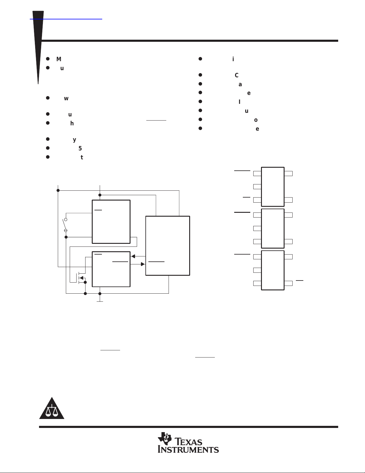
2.5 V 1.2 V
≥ V
DD
V
DD
MR
TPS3125J12
GND
IT
RESET
CV
TMS320UVC5402
DD
DV
DD
typical applications
D
Applications Using Low Voltage DSPs,
Microcontrollers or Microprocessors
D
Wireless Communication Systems
D
Portable/Battery-Powered Equipment
D
Programmable Controls
D
Intelligent Instruments
D
Industrial Equipment
D
Notebook/Desktop Computers
D
Automotive Systems
DBV PACKAGE
(TOP VIEW)
1
TPS3123
2
3
1
TPS3124
2
3
5
4
5
4
RESET
GND
MR
RESET
GND
RESET
V
DD
WDI
V
DD
WDI
MR
V
RESET
DD
TPS3823-25
GND
WDI
XF
RESET
GND
RESET
GND
RESET
1
TPS3125
2
3
V
5
4
DD
MR
Figure 1. Typical Dual-Voltage DSP Application
description
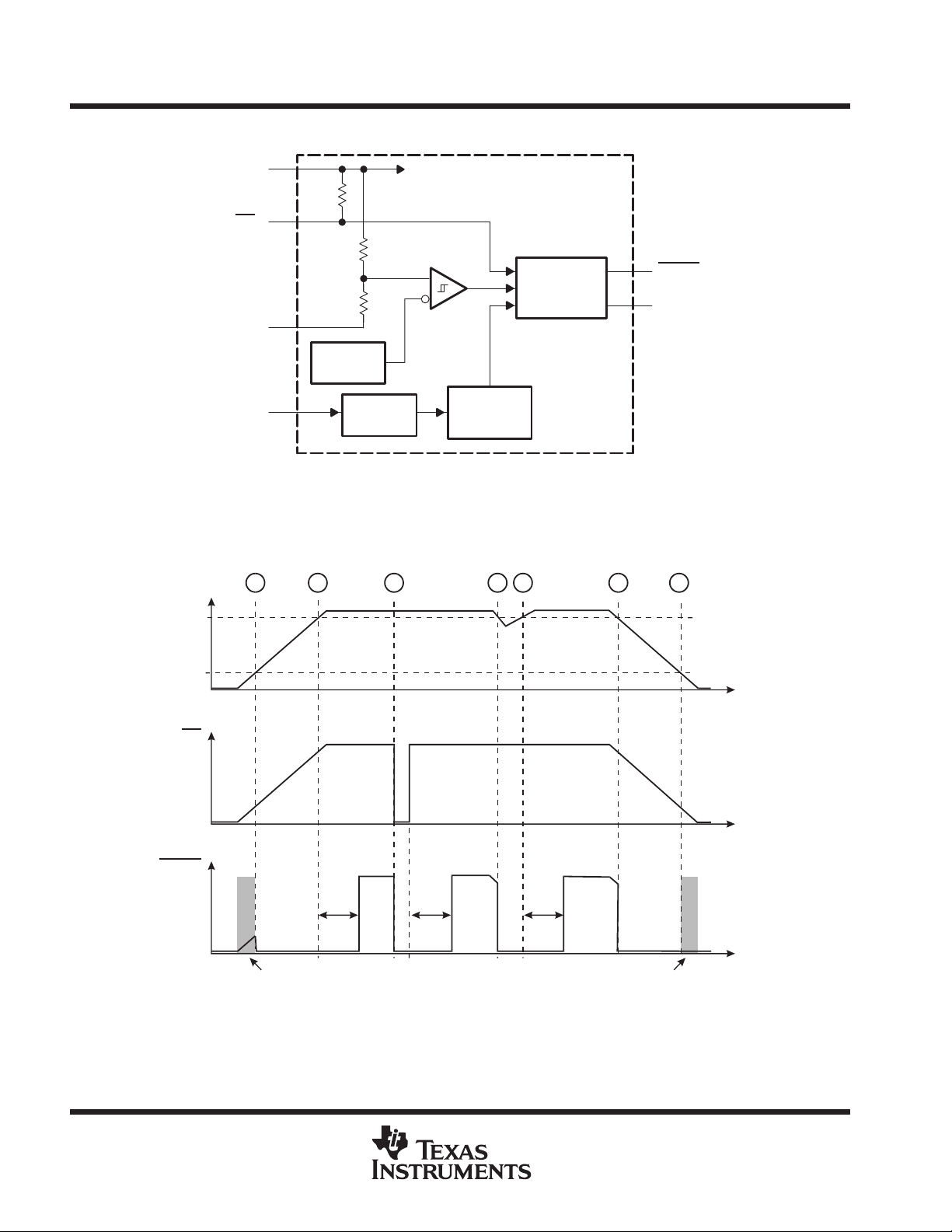
The TPS3123, TPS3124, TPS3125 family of ultra-low voltage processor supervisory circuits provides circuit
initialization and timing supervision, primarily for DSP and processor-based systems.
During power-on, RESET
the supply voltage supervisor monitors V
threshold voltage VIT. An internal timer delays the return of the output to the inactive state (high) to ensure proper
system reset. The delay time, t
Please be aware that an important notice concerning availability, standard warranty, and use in critical applications of
Texas Instruments semiconductor products and disclaimers thereto appears at the end of this data sheet.
is asserted when the supply voltage (VDD) becomes higher than 0.75 V . Thereafter,
and keeps RESET output active as long as VDD remains below the
DD
= 180 ms starts after VDD has risen above the threshold voltage VIT.
dtyp
PRODUCTION DATA information is current as of publication date.
Products conform to specifications per the terms of Texas Instruments
standard warranty. Production processing does not necessarily include
testing of all parameters.
POST OFFICE BOX 655303 • DALLAS, TEXAS 75265
Copyright 1999, Texas Instruments Incorporated
1
TPS3123J12, TPS3123G15, TPS3123J18, TPS3124J12, TPS3124G15
40°C to 85_C
TPS3124J18, TPS3125J12, TPS3125G15, TPS3125J18, TPS3125L30
ULTRA-LOW VOLTAGE PROCESSOR SUPERVISORY CIRCUITS
SLVS227 – AUGUST 1999
description (continued)
When the supply voltage drops below the threshold voltage VIT, the output becomes active (low) again. No
external components are required. All the devices of this family have a fixed-sense threshold voltage VIT set
by an internal voltage divider.
The TPS3123-xx and TPS3125-xx devices incorporate a manual reset input, MR. A low level at MR causes
RESET
RESET same as the TPS3125-xx devices. In addition the TPS3123-xx and TPS3124-xx have a watchdog timer
that need to be triggered periodically by a positive or negative transition at WDI. When the supervising system
fails to retrigger the watchdog circuit within the time-out interval t
the time period td. This event also reinitializes the watchdog timer.
The circuits are available in a 5-pin SOT23-5 package. The TPS3123, TPS3124, TPS3125 devices are
characterized for operation over a temperature range of –40°C to 85°C.
to become active. The TPS3124-xx devices do not have the input MR, but include a high-level output
= 0.8 s, RESET output becomes active for
tout
PACKAGE INFORMATION STANDARD VERSIONS
T
A
TPS3123J12DBVR
TPS3123G15DBVR†TPS3123G15DBVT
TPS3123J18DBVR
TPS3124J12DBVR
°
–
†
The DBVR passive indicates tape and reel of 3000 parts.
‡
The DBVT passive indicates tape and reel of 250 parts.
TPS3124G15DBVR†TPS3124G15DBVT
_
TPS3124J18DBVR
TPS3125J12DBVR
TPS3125G15DBVR†TPS3125G15DBVT
TPS3125J18DBVR
TPS3125L30DBVR
DEVICE NAME THRESHOLD VOLTAGE MARKING
†
TPS3123J12DBVT
†
TPS3123J18DBVT
†
TPS3124J12DBVT
†
TPS3124J18DBVT
†
TPS3125J12DBVT
†
TPS3125J18DBVT
†
TPS3125L30DBVT
‡
‡
‡
‡
‡
‡
‡
‡
‡
‡
1.08 V PBNI
1.40 V PBOI
1.62 V PBPI
1.08 V PBQI
1.40 V PBRI
1.62 V PBSI
1.08 V PBTI
1.40 V PBUI
1.62 V PBVI
2.64 V PBXI
2
POST OFFICE BOX 655303 • DALLAS, TEXAS 75265
TPS3123J12, TPS3123G15, TPS3123J18, TPS3124J12, TPS3124G15
TPS3124J18, TPS3125J12, TPS3125G15, TPS3125J18, TPS3125L30
ULTRA-LOW VOLTAGE PROCESSOR SUPERVISORY CIRCUITS
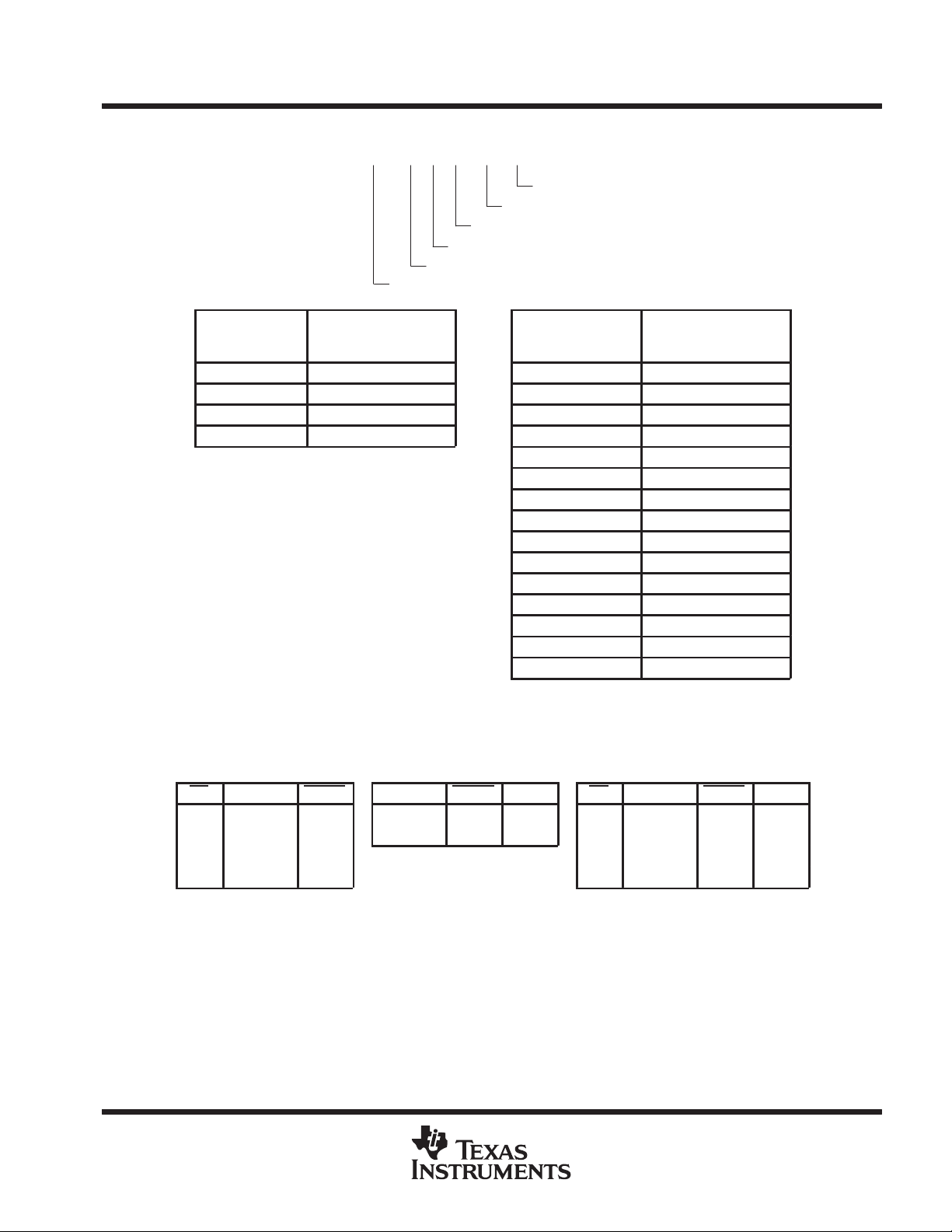
ordering information application specific versions
TPS312 3 J 12 DBV R
Nominal Supply Voltage
Typical Reset Threshold Voltage
Functionality
Family
SLVS227 – AUGUST 1999
Reel
Package
DEVICE NAME
TPS312xx12DBV 1.2 V TPS312xAxxDBV V
TPS312xx15DBV 1.5 V TPS312xBxxDBV V
TPS312xx18DBV 1.8 V TPS312xCxxDBV V
TPS312xx30DBV 3.0 V TPS312xDxxDBV V
NOTE: Ten standard versions will be available at product introduction.
For the application specific versions contact the local TI sales office for availability and lead time.
NOMINAL SUPPLY
VOLTAGE, V
NOM
DEVICE NAME
TPS312xExxDBV V
TPS312xFxxDBV V
TPS312xGxxDBV V
TPS312xHxxDBV V
TPS312xIxxDBV V
TPS312xJxxDBV V
TPS312xKxxDBV V
TPS312xLxxDBV V
TPS312xMxxDBV V
TPS312xNxxDBV V
TPS312xOxxDBV V
Function Tables
TPS3123 TPS3124 TPS3125
VDD > VITRESET VDD > VITRESET RESET MR VDD > VITRESET RESET
MR
L 0 L 0 L H L 0 L H
L 1 L 1 H L L 1 L H
H 0 L H 0 L H
H 1 H H 1 H L
TYPICAL RESET
THRESHOLD
VOLTAGE–V
NOM
NOM
NOM
NOM
NOM
NOM
NOM
NOM
NOM
NOM
NOM
NOM
NOM
NOM
NOM
IT–
–1%
–2%
–3%
–4%
–5%
–6%
–7%
–8%
–9%
–10%
–11%
–12%
–13%
–14%
–15%
POST OFFICE BOX 655303 • DALLAS, TEXAS 75265
3
TPS3123J12, TPS3123G15, TPS3123J18, TPS3124J12, TPS3124G15
TPS3124J18, TPS3125J12, TPS3125G15, TPS3125J18, TPS3125L30
ULTRA-LOW VOLTAGE PROCESSOR SUPERVISORY CIRCUITS
SLVS227 – AUGUST 1999
functional block diagram
V
DD
R1
†
MR
GND
Reference
Voltage
‡
WDI
†
TPS3123 and TPS3125 Only
‡
TPS3123 and TPS3124 Only
§
TPS3124 and TPS3125 Only
Transition
Detector
timing diagram TPS3123 and TPS3125
V
DD
V
IT
AB C DE F
R2
R3
Device Power Supply
Reset Logic
+ Timer
Watch Dog
Logic +
Timer
RESET
RESET
G
§
<0,85 V
MR
RESET
t
d
Output Undefined Output Undefined
t
d
t
d
t
t
t
4
POST OFFICE BOX 655303 • DALLAS, TEXAS 75265

TPS3123J12, TPS3123G15, TPS3123J18, TPS3124J12, TPS3124G15
TPS3124J18, TPS3125J12, TPS3125G15, TPS3125J18, TPS3125L30
ULTRA-LOW VOLTAGE PROCESSOR SUPERVISORY CIRCUITS
timing diagram TPS3123 and TPS3124
SLVS227 – AUGUST 1999
V
DD
V
<0,85 V
MR
(TPS3123)
WDI
RESET
AB
IT
G
CDE F
H
J
** ** *
t
d
t
d
t
d
t
d
t
t
t
t
d
t
tout
Output Undefined
t
tout
* = WDI Disabled
t
tout
t
POST OFFICE BOX 655303 • DALLAS, TEXAS 75265
5

TPS3123J12, TPS3123G15, TPS3123J18, TPS3124J12, TPS3124G15
Suppl
oltage, V
V
TPS3124J18, TPS3125J12, TPS3125G15, TPS3125J18, TPS3125L30
ULTRA-LOW VOLTAGE PROCESSOR SUPERVISORY CIRCUITS
SLVS227 – AUGUST 1999
absolute maximum ratings over operating free-air temperature (unless otherwise noted)
†
Supply voltage, VDD (see Note 1) 3.6 V. . . . . . . . . . . . . . . . . . . . . . . . . . . . . . . . . . . . . . . . . . . . . . . . . . . . . . . . . . .
All other pins (see Note 1) –0.3 V to 3.6 V. . . . . . . . . . . . . . . . . . . . . . . . . . . . . . . . . . . . . . . . . . . . . . . . . . . . . . . . .
Maximum low output current, IOL 5 mA. . . . . . . . . . . . . . . . . . . . . . . . . . . . . . . . . . . . . . . . . . . . . . . . . . . . . . . . . . .
Maximum high output current, I
Input clamp current, IIK (V
< 0 or VI > VDD) ±10 mA. . . . . . . . . . . . . . . . . . . . . . . . . . . . . . . . . . . . . . . . . . . . . . . .
I
–5 mA. . . . . . . . . . . . . . . . . . . . . . . . . . . . . . . . . . . . . . . . . . . . . . . . . . . . . . . . .
OH
Output clamp current, IOK (VO < 0 or VO > VDD) ±10 mA. . . . . . . . . . . . . . . . . . . . . . . . . . . . . . . . . . . . . . . . . . .
Continuous total power dissipation See Dissipation Rating Table. . . . . . . . . . . . . . . . . . . . . . . . . . . . . . . . . . . . .
Operating free-air temperature range, TA –40°C to 85°C. . . . . . . . . . . . . . . . . . . . . . . . . . . . . . . . . . . . . . . . . . .
Storage temperature range, T
–65°C to 150°C. . . . . . . . . . . . . . . . . . . . . . . . . . . . . . . . . . . . . . . . . . . . . . . . . .
stg
Soldering temperature 260°C. . . . . . . . . . . . . . . . . . . . . . . . . . . . . . . . . . . . . . . . . . . . . . . . . . . . . . . . . . . . . . . . . . . .
†
Stresses beyond those listed under “absolute maximum ratings” may cause permanent damage to the device. These are stress ratings only, and
functional operation of the device at these or any other conditions beyond those indicated under “recommended operating conditions” is not
implied. Exposure to absolute-maximum-rated conditions for extended periods may affect device reliability.
NOTE 1: All voltage values are with respect to GND.
DISSIPATION RATING TABLE
PACKAGE
DBV 437 mW 3.5 mW/°C 280 mW 227 mW
TA ≤ 25°C
POWER RATING
DERATING FACTOR
ABOVE TA = 25°C
TA = 70°C
POWER RATING
TA = 85°C
POWER RATING
recommended operating conditions at specified temperature range
MIN MAX UNIT
pp
y v
Input voltage, V
High-level input voltage, V
Low-level input voltage, V
Input transition rise and fall rate at WDI, ∆t/∆V 1 µs/V
Operating free-air temperature range, T
DD
I
IH
IL
A
TA = 0°C to 85°C 0.75 3.3
TA = –40°C to 85°C 0.85 3.3
0 VDD+0.3 V
0.7×V
DD
0.3×V
DD
–40 85 °C
V
V
6
POST OFFICE BOX 655303 • DALLAS, TEXAS 75265

TPS3123J12, TPS3123G15, TPS3123J18, TPS3124J12, TPS3124G15
IIHHigh-level input current
A
IILLow-level input current
A
RESET
VOHHigh-level output voltage
0.8×VDDV
RESET
RESET
VOLLow-level output voltage
V
RESET
V
ggg
T
40°C to 85°C
V
y
DD
,
IDDSupply current
A
MR unconnected
TPS3124J18, TPS3125J12, TPS3125G15, TPS3125J18, TPS3125L30
ULTRA-LOW VOLTAGE PROCESSOR SUPERVISORY CIRCUITS
SLVS227 – AUGUST 1999
electrical characteristics over recommended operating free-air temperature range (unless
otherwise noted)
PARAMETER TEST CONDITIONS MIN TYP MAX UNIT
MR pullup resistor (internal) 27 kΩ
p
p
p
p
Negative-going input threshold
IT–
voltage (see Note 2)
V
Hysteresis at VDD input
hys
pp
C
Input capacitance at MR, WDI VI = 0 V to 3.3 V 5 pF
i
NOTES: 2. To ensure best stability of the threshold voltage, a bypass capacitor (ceramic, 0.1 µF) should be placed near the supply terminal.
3. The supply current during delay time td is typical 5 µA higher.
WDI WDI = VDD = 3.3 V –1 1
MR MR = 0.7×VDD, VDD = 3.3 V –20 –55
WDI WDI = 0 V, VDD = 3.3 V –1 1
MR MR = 0 V, VDD = 3.3 V –80 –170
VDD = 1.5 V, IOH = –1 mA
VDD = 3.3 V, IOH = –4.5 mA
VDD = 0.75 V, IOH = –8 µA
VDD = 1.5 V, IOH = –1 mA
VDD = 0.75 V, IOL = 15 µA
VDD = 1.5 V, IOL = 1.4 mA
VDD = 1.5 V, IOL = 1.4 mA
VDD = 3.3 V, IOL = 3 mA 0.4
TPS312xJ12 1.04 1.08 1.12
TPS312xG15
TPS312xJ18
TPS312xL30 2.57 2.64 2.71
1 V < V
1.4 V < V
2 V < V
TPS3123-xx WDI = V
TPS3124-xx
TPS3125-xx
(see Note 3)
MR unconnected
A
°
= –
IT–
IT–
°
< 1.4 V 15
<2 V 20
IT–
< 3 V 30
,
VDD = 0.75 V 14
VDD = 3.3 V 22 30
VDD = 0.75 V 14
VDD = 3.3 V 18 25
1.35 1.40 1.45
1.56 1.62 1.68
0.2×V
DD
µ
µ
mV
µ
POST OFFICE BOX 655303 • DALLAS, TEXAS 75265
7
TPS3123J12, TPS3123G15, TPS3123J18, TPS3124J12, TPS3124G15
V
V
V
V
V
V
V
V
s
V
V
0.2 V
TPS3124J18, TPS3125J12, TPS3125G15, TPS3125J18, TPS3125L30
ULTRA-LOW VOLTAGE PROCESSOR SUPERVISORY CIRCUITS
SLVS227 – AUGUST 1999
timing requirements at RL = 1 MΩ, CL = 50 pF, TA = 25°C
PARAMETER TEST CONDITIONS MIN TYP MAX UNIT
At V
t
w
Pulse width
At MR
At WDI
switching characteristics at RL = 1 MΩ, CL = 50 pF, TA = 25°C
PARAMETER TEST CONDITIONS MIN TYP MAX UNIT
t
Watchdog time out
tout
t
Delay time
d
t
Propagation delay time, high-to-low-level output
PHL
t
Propagation delay time, low-to-high-level output
PLH
t
Propagation delay time, high-to-low-level output VDD to RESET delay
PHL
t
Propagation delay time, low-to-high-level output
PLH
DD
VIH = V
≥
DD
+0.2 V, VIL = V
IT–
+0.2 V,
IT–
MR to RESET delay
(TPS3123/25 only)
MR to RESET delay
(TPS3125 only)
VDD to RESET delay
(TPS3124/25 only)
= 0.3x
IL
–0,2 V 6
IT–
DD
,
= 0.7×
IH
VDD ≥ V
See timing diagram
VDD > V
See timing diagram
VDD ≥ V
= 0.2 ×
IL
VIH = 0.8 × V
=
IL
VIH = V
IT–
IT–
IT–
IT–
IT–
DD
+0.2 V,
+0.2 V,
+0.2 V,
DD
DD
–
+0.2 V
1
0.1
0.8 1.4 2.1 s
100 180 260 ms
,
,
0.1
0.1
10
10
µs
µ
µs
8
POST OFFICE BOX 655303 • DALLAS, TEXAS 75265

TPS3123J12, TPS3123G15, TPS3123J18, TPS3124J12, TPS3124G15
TPS3124J18, TPS3125J12, TPS3125G15, TPS3125J18, TPS3125L30
ULTRA-LOW VOLTAGE PROCESSOR SUPERVISORY CIRCUITS
SLVS227 – AUGUST 1999
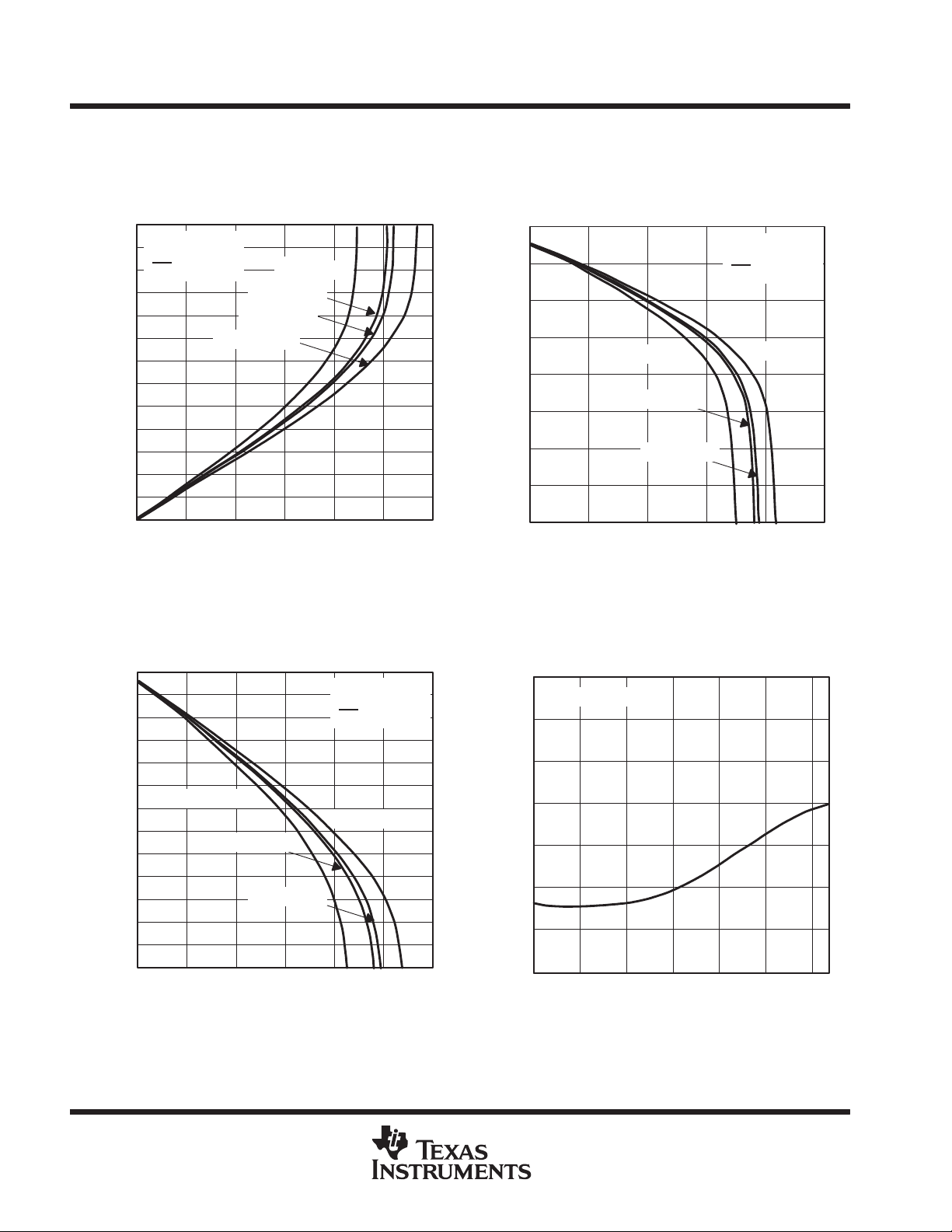
TYPICAL CHARACTERISTICS
SUPPLY CURRENT
vs
SUPPLY VOLTAGE
25
TA = 25°C
Aµ
20
15
– Supply Current –
CC
I
10
0
012
VDD – Supply Voltage – V
Figure 2
LOW-LEVEL OUTPUT VOLTAGE
vs
LOW-LEVEL OUTPUT CURRENT
850
TPS3123J12
800
700
600
500
400
VDD = 0.85 V
= Open
MR
TA = 85°C
TA = 25°C
TA = 0°C
TA = –40°C
TPS3123J12
3 3.3
LOW-LEVEL OUTPUT VOLTAGE
LOW-LEVEL OUTPUT CURRENT
750
TPS3123J12
VDD = 0.75 V
500
250
– Low-Level Output Voltage – mV
OL
V
0
0 50 100 150
IOL – Low-Level Output Current – µA
LOW-LEVEL OUTPUT VOLTAGE
LOW-LEVEL OUTPUT CURRENT
1.5
TPS3125L30
VDD = 1.5 V
= Open
MR
1.25
1
0.75
vs
TA = 85°C
TA = 25°C
TA = 0°C
200 250
Figure 3
vs
TA = 85°C
TA = 25°C
TA = 0°C
TA = –40°C
300
200
– Low-Level Output Voltage – mV
OL
V
100
0
0 100 200 300
IOL – Low-Level Output Current – µA
Figure 4
0.5
– Low-Level Output Voltage – V
0.25
OL
V
400 500
POST OFFICE BOX 655303 • DALLAS, TEXAS 75265
0
01 23
456
IOL – Low-Level Output Current – mA
Figure 5
9
TPS3123J12, TPS3123G15, TPS3123J18, TPS3124J12, TPS3124G15
TPS3124J18, TPS3125J12, TPS3125G15, TPS3125J18, TPS3125L30
ULTRA-LOW VOLTAGE PROCESSOR SUPERVISORY CIRCUITS
SLVS227 – AUGUST 1999
TYPICAL CHARACTERISTICS
LOW-LEVEL OUTPUT VOLTAGE
LOW-LEVEL OUTPUT CURRENT
3.3
TPS3125L30
3
VDD = 3.3 V
= Open
MR
2.75
2.5
2.25
2
1.75
1.5
1.25
1
– Low-Level Output Voltage – V
0.75
OL
0.5
V
0.25
0
0 5 10 15
IOL – Low-Level Output Current – mA
HIGH-LEVEL OUTPUT VOLTAGE
HIGH-LEVEL OUTPUT CURRENT
3.4
3
2.75
2.5
2.25
2
1.75
1.5
1.25
1
0.75
– High-Level Output Voltage – V
OH
0.5
V
0.25
0
0 –5 –10 –15
IOH – High-Level Output Current – mA
TA = –40°C
Figure 6
TA = 85°C
TA = 25°C
Figure 8
vs
TA = 85°C
TA = 25°C
TA = 0°C
vs
TA = 0°C
20 25 30
TPS3123J12
VDD = 3.3 V
MR
= Open
TA = –40°C
–20 –25 –30
1.6
1.4
1.2
0.8
0.6
0.4
– High-Level Output Voltage – V
OH
V
0.2
1.005
(25 )°C
IT
V
1.004
A
(T )/
IT
1.003
V
1.002
1.001
0.999
0.998
Normalized Input Threshold Voltage –
HIGH-LEVEL OUTPUT VOLTAGE
vs
HIGH-LEVEL OUTPUT CURRENT
TPS3123J12
VDD = 1.5 V
MR
= Open
1
TA = 85°C
TA = 25°C
TA = 0°C
0
0–1–2–3
IOH – High-Level Output Current – mA
TA = –40°C
–4 –5
Figure 7
NORMALIZED INPUT THRESHOLD VOLTAGE
vs
FREE-AIR TEMPERATURE
TPS312xJ12
1
–40 –20 0 20 40
TA – Free-Air Temperature – °C
60 80
Figure 9
10
POST OFFICE BOX 655303 • DALLAS, TEXAS 75265

TPS3123J12, TPS3123G15, TPS3123J18, TPS3124J12, TPS3124G15
TPS3124J18, TPS3125J12, TPS3125G15, TPS3125J18, TPS3125L30
ULTRA-LOW VOLTAGE PROCESSOR SUPERVISORY CIRCUITS
SLVS227 – AUGUST 1999
TYPICAL CHARACTERISTICS
NORMALIZED INPUT THRESHOLD VOLTAGE
FREE-AIR TEMPERATURE
1.005
(25 )°C
IT
V
1.004
A
(T )/
IT
1.003
V
1.002
1.001
0.999
0.998
Normalized Input Threshold Voltage –
TPS312xL30
1
–40 –20 0 20 40
TA – Free-Air Temperature – °C
Figure 10
vs
vs
THRESHOLD OVERDRIVE
MINIMUM PULSE DURATION
4.5
MR = Open
VIT = 2.64 V
TA = 25°C
200 250 300
60 80
4
sµ
3.5
3
2.5
2
1.5
– Minimum Pulse Duration –
1
w
t
0.5
0
0 50 100 150
TPS312xL30
VDD – Threshold Overdrive – mV
Figure 11
MINIMUM PULSE DURATION
vs
THRESHOLD OVERDRIVE
3.5
MR = Open
3
sµ
2.5
TPS312xJ12
VIT = 1.08 V
TA = 25°C
2
1.5
1
– Minimum Pulse Duration –
w
t
0.5
0
0 50 100 150
VDD – Threshold Overdrive – mV
Figure 12
POST OFFICE BOX 655303 • DALLAS, TEXAS 75265
200 250 300
11

TPS3123J12, TPS3123G15, TPS3123J18, TPS3124J12, TPS3124G15
TPS3124J18, TPS3125J12, TPS3125G15, TPS3125J18, TPS3125L30
ULTRA-LOW VOLTAGE PROCESSOR SUPERVISORY CIRCUITS
SLVS227 – AUGUST 1999
MECHANICAL DATA
DBV (R-PDSO-G5) PLASTIC SMALL-OUTLINE
0,95
0,95
1,45
3,00
2,80
45
31
0,05 MIN
0,50
0,30
1,70
1,50
M
0,20
3,00
2,60
Seating Plane
0,10
0,15 NOM
Gage Plane
0°–8°
0,25
0,55
0,35
NOTES: A. All linear dimensions are in millimeters.
B. This drawing is subject to change without notice.
C. Body dimensions do not include mold flash or protrusion.
D. Falls within JEDEC MO-178
4073253-4/E 05/99
12
POST OFFICE BOX 655303 • DALLAS, TEXAS 75265

IMPORTANT NOTICE
T exas Instruments and its subsidiaries (TI) reserve the right to make changes to their products or to discontinue
any product or service without notice, and advise customers to obtain the latest version of relevant information
to verify, before placing orders, that information being relied on is current and complete. All products are sold
subject to the terms and conditions of sale supplied at the time of order acknowledgement, including those
pertaining to warranty, patent infringement, and limitation of liability.
TI warrants performance of its semiconductor products to the specifications applicable at the time of sale in
accordance with TI’s standard warranty. Testing and other quality control techniques are utilized to the extent
TI deems necessary to support this warranty . Specific testing of all parameters of each device is not necessarily
performed, except those mandated by government requirements.
CERTAIN APPLICA TIONS USING SEMICONDUCT OR PRODUCTS MAY INVOLVE POTENTIAL RISKS OF
DEATH, PERSONAL INJURY, OR SEVERE PROPERTY OR ENVIRONMENTAL DAMAGE (“CRITICAL
APPLICATIONS”). TI SEMICONDUCTOR PRODUCTS ARE NOT DESIGNED, AUTHORIZED, OR
WARRANTED TO BE SUITABLE FOR USE IN LIFE-SUPPORT DEVICES OR SYSTEMS OR OTHER
CRITICAL APPLICA TIONS. INCLUSION OF TI PRODUCTS IN SUCH APPLICATIONS IS UNDERST OOD TO
BE FULLY AT THE CUSTOMER’S RISK.
In order to minimize risks associated with the customer’s applications, adequate design and operating
safeguards must be provided by the customer to minimize inherent or procedural hazards.
TI assumes no liability for applications assistance or customer product design. TI does not warrant or represent
that any license, either express or implied, is granted under any patent right, copyright, mask work right, or other
intellectual property right of TI covering or relating to any combination, machine, or process in which such
semiconductor products or services might be or are used. TI’s publication of information regarding any third
party’s products or services does not constitute TI’s approval, warranty or endorsement thereof.
Copyright 1999, Texas Instruments Incorporated
 Loading...