

1
FEATURES
DESCRIPTION
APPLICATIONS
TPS28226
SLUS791 – OCTOBER 2007
www.ti.com
High-Frequency 4-A Sink Synchronous MOSFET Drivers
• Drives Two N-Channel MOSFETs with 14-ns
Adaptive Dead Time
The TPS28226 is a high-speed driver for N-channel
complimentary driven power MOSFETs with adaptive
• Gate Drive Voltage: 6.8 V Up to 8.8 V
dead-time control. This driver is optimized for use in
• Wide Power System Train Input Voltage: 3 V
variety of high-current one and multi-phase dc-to-dc
Up to 27 V
converters. The TPS28226 is a solution that provides
• Wide Input PWM Signals: 2.0 V up to 13.2-V
highly efficient, small size low EMI emmissions.
Amplitude
The performance is achieved by up to 8.8-V gate
• Capable Drive MOSFETs with ≥ 40-A Current
drive voltage, 14-ns adaptive dead-time control, 14-ns
per Phase
propagation delays and high-current 2-A source and
4-A sink drive capability. The 0.4- Ω impedance for
• High Frequency Operation: 14-ns Propagation
the lower gate driver holds the gate of power
Delay and 10-ns Rise/Fall Time Allow F
SW
- 2
MOSFET below its threshold and ensures no
MHz
shoot-through current at high dV/dt phase node
• Capable Propagate <30-ns Input PWM Pulses
transitions. The bootstrap capacitor charged by an
• Low-Side Driver Sink On-Resistance (0.4 Ω )
internal diode allows use of N-channel MOSFETs in
Prevents dV/dT Related Shoot-Through
half-bridge configuration.
Current
The TPS28226 features a 3-state PWM input
• 3-State PWM Input for Power Stage Shutdown
compatible with all multi-phase controllers employing
3-state output feature. As long as the input stays
• Space Saving Enable (input) and Power Good
within 3-state window for the 250-ns hold-off time, the
(output) Signals on Same Pin
driver switches both outputs low. This shutdown
• Thermal Shutdown
mode prevents a load from the reversed-
• UVLO Protection
output-voltage.
• Internal Bootstrap Diode
The other features include under voltage lockout,
• Economical SOIC-8 and Thermally Enhanced
thermal shutdown and two-way enable/power good
3-mm x 3-mm DFN-8 Packages
signal. Systems without 3-state featured controllers
can use enable/power good input/output to hold both
• High Performance Replacement for Popular
outputs low during shutting down.
3-State Input Drivers
The TPS28226 is offered in an economical SOIC-8
and thermally enhanced low-size Dual Flat No-Lead
(DFN-8) packages. The driver is specified in the
• Multi-Phase DC-to-DC Converters with Analog
extended temperature range of – 40 ° C to 125 ° C with
or Digital Control
the absolute maximum junction temperature 150 ° C.
• Desktop and Server VRMs and EVRDs
• Portable/Notebook Regulators
• Synchronous Rectification for Isolated Power
Supplies
1
Please be aware that an important notice concerning availability, standard warranty, and use in critical applications of
Texas Instruments semiconductor products and disclaimers thereto appears at the end of this data sheet.
UNLESS OTHERWISE NOTED this document contains
Copyright © 2007, Texas Instruments Incorporated
PRODUCTION DATA information current as of publication date.
Products conform to specifications per the terms of Texas
Instruments standard warranty. Production processing does not
necessarily include testing of all parameters.
www.ti.com
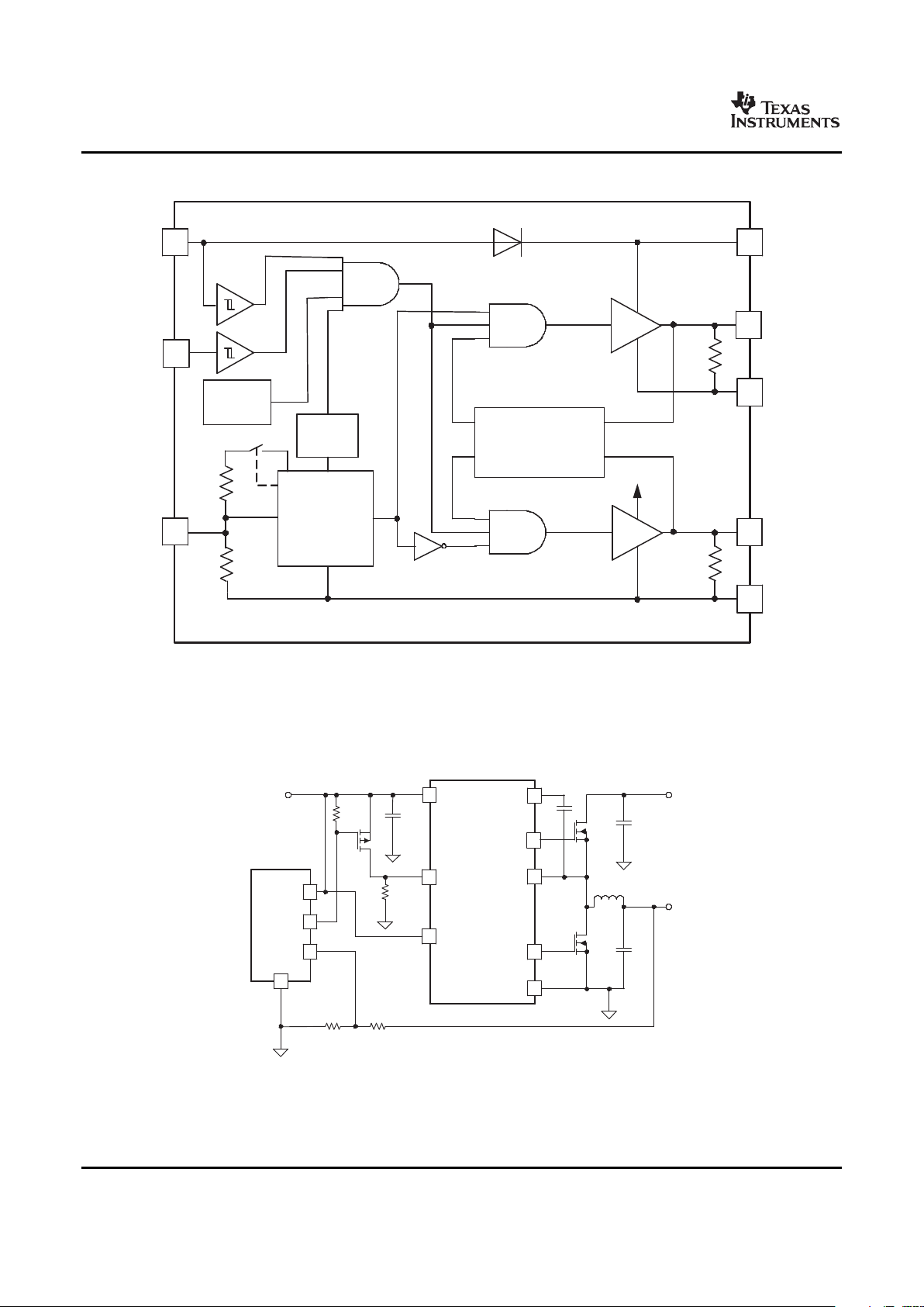
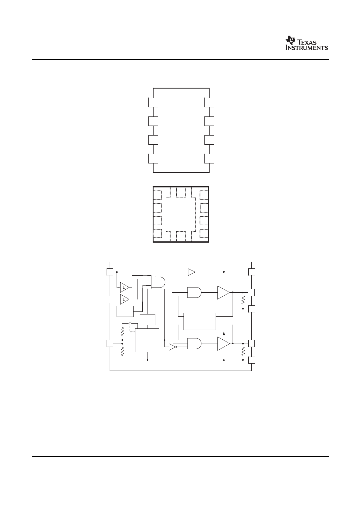
FUNCTIONAL BLOCK DIAGRAM
6
13K
2
VDD
EN / PG
BOOT
UGATE
PHASE
LGATE
GND
7
1
8
5
4
VDD
27K
3 −STATE
INPUT
CIRCUIT
PWM
3
SHOOT −
THROUGH
PROTECTION
THERMAL
SD
HLD−OFF
TIME
UVLO
TYPICAL APPLICATIONS
3
3
2
BOOT
UGATE
PHASE
LGATE
GND
1
8
5
4
6
VDD
ENBL
7
PWM
3
OUT
FB
3
GND
3
TPS28226
VC (6.8 V to 8 V)
VIN (3 V to 32 V − VDD)
V
OUT
VCC
TPS40200
TPS28226
SLUS791 – OCTOBER 2007
One-Phase POL Regulator
2 Submit Documentation Feedback Copyright © 2007, Texas Instruments Incorporated
Product Folder Link(s): TPS28226

www.ti.com
PWM
CONTROLLER
ISOLATION
AND
FEEDBACK
CONTROL
DRIVE
LO
DRIVE
HI
HI
LI
HB
HO
HS
LO
2
BOOT
UGATE
PHASE
LGATE
GND
1
8
5
4
3
VDD
EN/PG
7
PWM
6
LINEAR
REG.
VC (6.8 V to 8 V)
V
OUT
= 3.3 V
35 V to 75V
12 V
Primary High Side
VDD High Voltage Driver
V
SS
TPS28226
TPS28226
SLUS791 – OCTOBER 2007
TYPICAL APPLICATIONS (continued)
Driver for Synchronous Rectification with Complementary Driven MOSFETs
Copyright © 2007, Texas Instruments Incorporated Submit Documentation Feedback 3
Product Folder Link(s): TPS28226

www.ti.com
5
4
7 3
8
1
2
2
BOOT
UGATE
PHASE
LGATE
GND
1
8
5
4
6 VDD
EN/PG
7
PWM
3
2
BOOT
UGATE
PHASE
LGATE
GND
1
8
5
4
6 VDD
EN
/PG
7
PWM
3
VIN
PWM4
GND
VOUT
PWM1
8
PWM3
Enable
PWM2
To Driver
To Driver
GNDS
To Controller
CSCNCS 4
To Controller
CS 1
VC (6.8 V to 8 V)
VIN (3 V to 32 V − VDD)
TPS28226
TPS28226
TPS4009x
or any other analog
or digital controller
V
OUT
TPS28226
SLUS791 – OCTOBER 2007
TYPICAL APPLICATIONS (continued)
Multi-Phase Synchronous Buck Converter
ORDERING INFORMATION
(1) (2) (3)
PART NUMBER
TEMPERATURE RANGE, TA= T
J
PACKAGE TAPE AND REEL QTY.
TPS28226
Plastic 8-pin SOIC (D) 75 per tube TPS28226D
Plastic 8-pin SOIC (D) 2500 TPS28226DR
-40C to 125C
Plastic 8-pin DFN (DRB) 250 TPS28226DRBT
Plastic 8-pin DFN (DRB) 3000 TPS28226DRBR
(1) SOIC-8 (D) and DFN-8 (DRB) packages are available taped and reeled. Add T suffix to device type (e.g. TPS28226DRBT) to order
taped devices and suffix R (e.g. TPS28226DRBR) to device type to order reeled devices.
(2) The SOIC-8 (D) and DFN-8 (DRB) package uses in Pb-Free lead finish of Pd-Ni-Au which is compatible with MSL level 1 at 255C to
260C peak reflow temperature to be compatible with either lead free or Sn/Pb soldering operations.
(3) In the DFN package, the pad underneath the center of the device is a thermal substrate. The PCB “ thermal land ” design for this
exposed die pad should include thermal vias that drop down and connect to one or more buried copper plane(s). This combination of
vias for vertical heat escape and buried planes for heat spreading allows the DFN to achieve its full thermal potential. This pad should
be either grounded for best noise immunity, and it should not be connected to other nodes.
4 Submit Documentation Feedback Copyright © 2007, Texas Instruments Incorporated
Product Folder Link(s): TPS28226
www.ti.com
ABSOLUTE MAXIMUM RATINGS
DISSIPATION RATINGS
(1)
RECOMMENDED OPERATING CONDITIONS
TPS28226
SLUS791 – OCTOBER 2007
over operating free-air temperature range (unless otherwise noted)
(1) (2)
TPS28226 VALUE UNIT
Input supply voltage range, V
DD
(3)
– 0.3 to 8.8
Boot voltage, V
BOOT
– 0.3 to 33
DC – 2 to 32 or V
BOOT
+ 0.3 – V
DD
whichever is less
Phase voltage, V
PHASE
Pulse < 400 ns, E = 20 μ J – 7 to 33.1 or V
BOOT
+ 0.3 – V
DD
whichever is less
Input voltage range, V
PWM
, V
EN/PG
– 0.3 to 13.2
V
PHASE
– 0.3 to V
BOOT
+ 0.3, (V
BOOT
– V
PHASE
< 8.8) V
Output voltage range, V
UGATE
Pulse < 100 ns, E = 2 μ J V
PHASE
– 2 to V
BOOT
+ 0.3, (V
BOOT
– V
PHASE
< 8.8)
– 0.3 to V
DD
+ 0.3
Output voltage range, V
LGATE
Pulse < 100 ns, E = 2 μ J – 2 to V
DD
+ 0.3
ESD rating, HBM 2 k
ESD rating, HBM ESD rating, CDM 500
Continuous total power dissipation See Dissipation Rating Table
Operating virtual junction temperature range, T
J
– 40 to 150
Operating ambient temperature range, T
A
– 40 to 125
° C
Storage temperature, T
stg
– 65 to 150
Lead temperature (soldering, 10 sec.) 300
(1) Stresses beyond those listed under “ absolute maximum ratings ” may cause permanent damage to the device. These are stress ratings
only, and functional operation of the device at these or any other conditions beyond those indicated under “ recommended operating
conditions ” is not implied. Exposure to absolute-maximum-rated conditions for extended periods may affect device reliability.
(2) These devices are sensitive to electrostatic discharge; follow proper device handling procedures.
(3) All voltages are with respect to GND unless otherwise noted. Currents are positive into, negative out of the specified terminal. Consult
Packaging Section of the Data book for thermal limitations and considerations of packages.
DERATING FACTOR TA< 25 ° C TA=70 ° C TA= 85 ° C
BOARD PACKAGE R
θ JC
R
θ JA
ABOVE TA= 25 ° C POWER RATING POWER RATING POWER RATING
High-K
(2)
D 39.4 ° C/W 100C/W 10 mW/C 1.25 W 0.8 W 0.65 W
High-K
(3)
DRB 1.4 ° C/W 48.5C/W 20.6 mW/C 2.58 W 1.65 W 1.34 W
(1) These thermal data are taken at standard JEDEC test conditions and are useful for the thermal performance comparison of different
packages. The cooling condition and thermal impedance R
θ JA
of practical design is specific.
(2) The JEDEC test board JESD51-7, 3-inch x 3-inch, 4-layer with 1-oz internal power and ground planes and 2-oz top and bottom trace
layers.
(3) The JEDEC test board JESD51-5 with direct thermal pad attach, 3-inch x 3-inch, 4-layer with 1-oz internal power and ground planes and
2-oz top and bottom trace layers.
over operating free-air temperature range (unless otherwise noted)
MIN TYP MAX UNIT
V
DD
Input supply voltage 6.8 7.2 8
V
V
IN
Power input voltage 3 32 V – VDD
T
J
Operating junction temperature range – 40 125 C
Copyright © 2007, Texas Instruments Incorporated Submit Documentation Feedback 5
Product Folder Link(s): TPS28226
www.ti.com
ELECTRICAL CHARACTERISTICS
(1)
TPS28226
SLUS791 – OCTOBER 2007
V
DD
= 7.2 V, EN/PG pulled up to V
DD
by 100-k Ω resistor, TA= TJ= – 40 ° C to 125 ° C (unless otherwise noted)
PARAMETER TEST CONDITIONS MIN TYP MAX UNIT
UNDER VOLTAGE LOCKOUT
Rising threshold 6.35 6.70
Falling threshold V
PWM
= 0 V 4.7 5.0 V
Hysteresis 1.00 1.35
BIAS CURRENTS
I
DD(off)
Bias supply current V
EN/PG
= low, PWM pin floating 350
μ A
I
DD
Bias supply current V
EN/PG
= high, PWM pin floating 500
INPUT (PWM)
V
PWM
= 5 V 185
I
PWM
Input current μ A
V
PWM
= 0 V – 200
PWM 3-state rising threshold
(2)
1.0
V
PWM 3-state falling threshold V
PWM
PEAK = 5 V 3.4 3.8 4.0
t
HLD_R
3-state shutdown Hold-off time 250
ns
T
MIN
PWM minimum pulse to force U
GATE
pulse CL= 3 nF at U
GATE
, V
PWM
= 5 V 30
ENABLE/POWER GOOD (EN/PG)
Enable high rising threshold PG FET OFF 1.7 2.1
Enable low falling threshold PG FET OFF 0.8 1.0
V
Hysteresis 0.35 0.70
Power good output V
DD
= 2.5 V 0.2
UPPER GATE DRIVER OUTPUT (UGATE)
Source resistance 500 mA source current 1.0 2.0 Ω
Source current
(2)
V
UGATE-PHASE
= 2.5 V 2.0 A
t
RU
Rise time CL= 3 nF 10 ns
Sink resistance 500 mA sink current 1.0 2.0 Ω
Sink current
(2)
V
UGATE-PHASE
= 2.5 V 2.0 A
t
FU
Fall time CL= 3 nF 10 ns
(1) Typical values for TA= 25C
(2) Not tested in production
6 Submit Documentation Feedback Copyright © 2007, Texas Instruments Incorporated
Product Folder Link(s): TPS28226
www.ti.com
TPS28226
SLUS791 – OCTOBER 2007
ELECTRICAL CHARACTERISTICS (continued)
V
DD
= 7.2 V, EN/PG pulled up to V
DD
by 100-k Ω resistor, TA= TJ= – 40 ° C to 125 ° C (unless otherwise noted)
PARAMETER TEST CONDITIONS MIN TYP MAX UNIT
LOWER GATE DRIVER OUTPUT (LGATE)
Source resistance 500 mA source current 1.0 2.0 Ω
Source current
(3)
V
LGATE
= 2.5 V 2.0 A
t
RL
Rise time
(3)
CL= 3 nF 10 ns
Sink resistance 500 mA sink current 0.4 1.0 Ω
Sink current
(3)
V
LGATE
= 2.5 V 4.0 A
Fall time
(3)
CL= 3 nF 5 ns
SWITCHING TIME
t
DLU
UGATE turn-off propagation Delay CL= 3 nF 14
t
DLL
LGATE turn-off propagation Delay CL= 3 nF 14
ns
t
DTU
Dead time LGATE turn-off to UGATE turn-on CL= 3 nF 14
t
DTL
Dead time UGATE turn-off to LGATE turn-on CL= 3 nF 14
BOOTSTRAP DIODE
V
F
Forward voltage Forward bias current 100 mA 1.0 V
THERMAL SHUTDOWN
Rising threshold
(3)
150 160 170
Falling threshold
(3)
130 140 150 ° C
Hysteresis 20
(3) Not tested in production
Copyright © 2007, Texas Instruments Incorporated Submit Documentation Feedback 7
Product Folder Link(s): TPS28226
www.ti.com
DEVICE INFORMATION
1
2
3
4
8
7
6
5
UGATE
BOOT
PWM
GND
PHASE
EN/PG
VDD
LGATE
5
3
7
6
81
2BOOT
PWM VDD
EN/PG
LG ATEGND
UG ATE PHASE
4
Exposed
Thermal
Die Pad
6
13K
2
VDD
EN /PG
BOOT
UGATE
PHASE
LGATE
GND
7
1
8
5
4
VDD
27K
3−STATE
INPUT
CIRCUIT
PWM
3
SHOOT −
THROUGH
PROTECTION
THERMAL
SD
HLD−OFF
TIME
UVLO
TPS28226
SLUS791 – OCTOBER 2007
SOIC-8 Package (top view)
DRB-8 Package (top view)
FUNCTIONAL BLOCK DIAGRAM
A. For the TPS28226DRB device the thermal PAD on the bottom side of package must be soldered and connected to
the GND pin and to the GND plane of the PCB in the shortest possible way. See Recommended Land Pattern in the
Application section.
8 Submit Documentation Feedback Copyright © 2007, Texas Instruments Incorporated
Product Folder Link(s): TPS28226
www.ti.com
TRUTH TABLE
TPS28226
SLUS791 – OCTOBER 2007
TERMINAL FUNCTIONS
TERMINAL
I/O DESCRIPTION
SOIC-8 DRB-8 NAME
1 1 UGATE O Upper gate drive sink/source output. Connect to gate of high-side power N-Channel MOSFET.
Floating bootstrap supply pin for the upper gate drive. Connect the bootstrap capacitor between
2 2 BOOT I/O this pin and the PHASE pin. The bootstrap capacitor provides the charge to turn on the upper
MOSFET.
The PWM signal is the control input for the driver. The PWM signal can enter three distinct states
3 3 PWM I during operation, see the 3-state PWM Input section under DETAILED DESCRIPTION for further
details. Connect this pin to the PWM output of the controller.
4 4 GND — Ground pin. All signals are referenced to this node.
Exposed Thermal
— Connect directly to the GND for better thermal performance and EMI
die pad pad
Lower gate drive sink/source output. Connect to the gate of the low-side power N-Channel
5 5 LGATE O
MOSFET.
6 6 VDD I Connect this pin to a 5-V bias supply. Place a high quality bypass capacitor from this pin to GND.
Enable/Power Good input/output pin with 1M Ω impedance. Connect this pin to HIGH to enable and
LOW to disable the device. When disabled, the device draws less than 350 μ A bias current. If the
7 7 EN/PG I/O
V
DD
is below UVLO threshold or over temperature shutdown occurs, this pin is internally pulled
low.
Connect this pin to the source of the upper MOSFET and the drain of the lower MOSFET. This pin
8 8 PHASE I
provides a return path for the upper gate driver.
V
DD
FALLING > 3 V AND TJ< 150 ° C
V
DD
RISING < 3.5 V EN/PG FALLING > 1.0 V
PIN
EN/PG RISING
OR TJ> 160 ° C
PWM > 1.5 V AND PWM SIGNAL SOURCE IMPEDANCE
< 1.7 V
PWM < 1 V
T
RISE
/T
FALL
< 200 ns >40 k Ω FOR > 250ns (3-State)
(1)
LGATE Low Low High Low Low
UGATE Low Low Low High Low
EN/PG Low
(1) During power up, the TPS28226 is in 3-state and both UGATE and LGATE outputs are kept low. To exit the 3-state condition, the PWM
signal should go high followed by one low PWM signal. The first high PWM pulse is ignored by the driver and keeps UGATE output low,
but the following low PWM signal drives LGATE high.
Copyright © 2007, Texas Instruments Incorporated Submit Documentation Feedback 9
Product Folder Link(s): TPS28226
www.ti.com
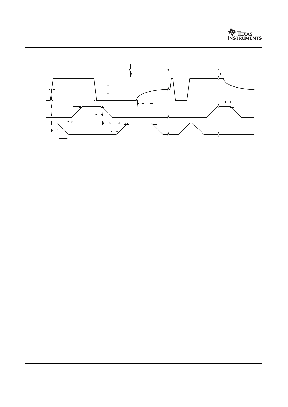
Normal switching
PWM
LGATE
UGATE
3-State
window
90%
10%
t
DLL
50%
t
FL
50%
t
PWM_MIN
t
DTU
90%
10%
t
RU
90%
10%
t
DLU
t
FU
t
DTL
90%
10%
t
RL
t
HLD_R
90%
10%
90%
90%
t
HLD_F
Enter into 3-State at
PWM rise
Exit 3-State
Enter into 3-State at
PWM fall
LGATE exits 3-State after PWM
goes High and then Low
TPS28226
SLUS791 – OCTOBER 2007
TPS28226 TIMING DIAGRAM
10 Submit Documentation Feedback Copyright © 2007, Texas Instruments Incorporated
Product Folder Link(s): TPS28226
www.ti.com
TYPICAL CHARACTERISTICS
−40 125
300
340
380
420
460
500
25
320
360
400
440
480
TJ − Temperature − °C
I
DD(off)
− Bias Supply − µA
2.00
3.50
4.50
6.00
2.50
3.00
4.00
5.00
5.50
UVLO − Under Voltage Lockout − V
−40 125
TJ − Temperature − C
25
6.50
8.00
7.00
7.50
TPS28226 Falling
TPS28226 Rising
0.0
PWM − PWM 3−State Threshold − V
−40 12525
2.0
3.0
5.0
0.5
1.0
2.5
2.5
4.5
1.5
4.0
Falling
Rising
TJ − Temperature − °C
−40 12525
0.00
0.75
1.25
2.00
0.25
0.50
1.00
1.50
1.75
Falling
Rising
TJ − Temperature − °C
EN/PG − Enable/Power Good − V
TPS28226
SLUS791 – OCTOBER 2007
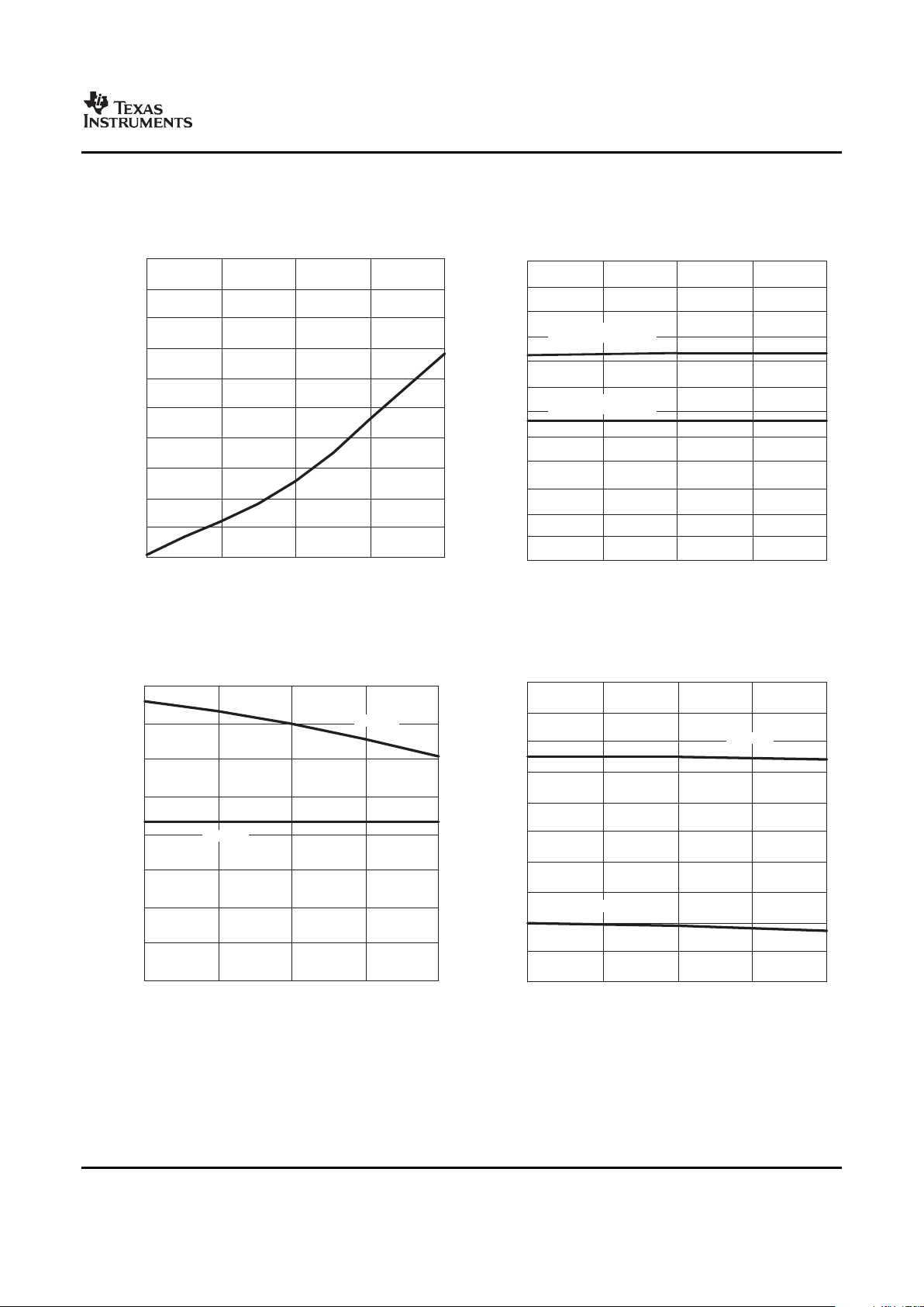
BIAS SUPPLY CURRENT
vs UNDER VOLTAGE LOCKOUT THRESHOLD
TEMPERATURE vs
(V
EN/PG
= Low, PWM Input Floating, V
DD
= 7.2V) TEMPERATURE
Figure 1. Figure 2.
ENABLE/POWER GOOD THRESHOLD PWM 3-STATE THRESHOLDS, (5-V Input Pulses)
vs vs
TEMPERATURE (V
DD
= 7.2 V) TEMPERATURE, (V
DD
= 7.2 V)
Figure 3. Figure 4.
Copyright © 2007, Texas Instruments Incorporated Submit Documentation Feedback 11
Product Folder Link(s): TPS28226
 Loading...