


www.ti.com
FEATURES DESCRIPTION
APPLICATIONS
TPS28225
SLUS710 – MAY 2006
High-Frequency 4-A Sink Synchronous MOSFET Driver
• Drives Two N-Channel MOSFETs with 14-ns
The TPS28225 is a high-speed driver for N-channel
Adaptive Dead Time
complimentary driven power MOSFETs with adaptive
dead-time control. This driver is optimized for use in
• Wide Gate Drive Voltage: 4.5V Up to 8.8V
variety of high-current one and multi-phase dc-to-dc
With Best Efficiency at 7V to 8V
converters. The TPS28225 is a solution that provides
• Wide Power System Train Input Voltage: 3V
highly efficient, small size low EMI emmissions.
Up to 27V
The performance is achieved by up to 8.8-V gate
• Wide Input PWM Signals: 2.0V up to 13.2-V
drive voltage, 14-ns adaptive dead-time control,
Amplitude
14-ns propagation delays and high-current 2-A
• Capable Drive MOSFETs with ≥ 40-A Current
source and 4-A sink drive capability. The 0.4- Ω
per Phase
impedance for the lower gate driver holds the gate of
power MOSFET below its threshold and ensures no
• High Frequency Operation: 14ns Propagation
shoot-through current at high dV/dt phase node
Delay and 10ns Rise/Fall Time Allow Fsw -
transitions. The bootstrap capacitor charged by an
2MHz
internal diode allows use of N-channel MOSFETs in
• Capable Propagate <30-ns Input PWM Pulses
half-bridge configuration.
• Low-Side Driver Sink On-Resistance (0.4 Ω )
The TPS28225 features a 3-state PWM input
Prevents dV/dT Related Shoot-Through
compatible with all multi-phase controllers employing
Current
3-state output feature. As long as the input stays
• 3-State PWM Input for Power Stage Shutdown
within 3-state window for the 250-ns hold-off time,
the driver switches both outputs low. This shutdown
• Space Saving Enable (input) and Power Good
mode prevents a load from the reversed-
(output) Signals on Same Pin
output-voltage.
• Thermal Shutdown
The other features include under voltage lockout,
• UVLO Protection
thermal shutdown and two-way enable/power good
• Internal Bootstrap Diode
signal. Systems without 3-state featured controllers
can use enable/power good input/output to hold both
• Economical SOIC-8 and Thermally Enhanced
outputs low during shutting down.
3-mm x 3-mm DFN-8 Packages
• High Performance Replacement for Popular
The TPS28225 is offered in an economical SOIC-8
3-State Input Drivers and thermally enhanced low-size Dual Flat No-Lead
(DFN-8) packages. The driver is specified in the
extended temperature range of –40 ° C to 125 ° C with
the absolute maximum junction temperature 150 ° C.
• Multi-Phase DC-to-DC Converters with
Analog or Digital Control
• Desktop and Server VRMs and EVRDs
• Portable/Notebook Regulators
• Synchronous Rectification for Isolated Power
Supplies
Please be aware that an important notice concerning availability, standard warranty, and use in critical applications of Texas
Instruments semiconductor products and disclaimers thereto appears at the end of this data sheet.
PRODUCTION DATA information is current as of publication date.
Copyright © 2006, Texas Instruments Incorporated
Products conform to specifications per the terms of the Texas
Instruments standard warranty. Production processing does not
necessarily include testing of all parameters.
www.ti.com
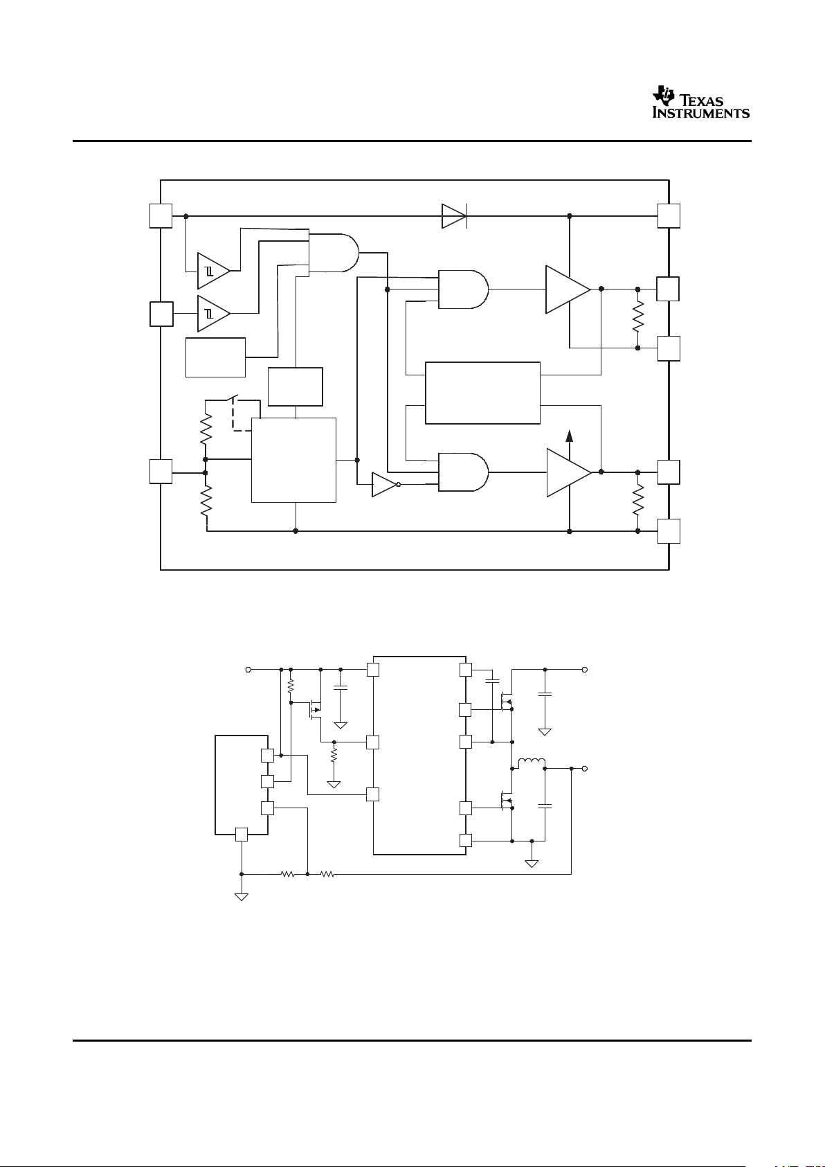
FUNCTIONAL BLOCK DIAGRAM
6
13K
2
VDD
EN / PG
BOOT
UGATE
PHASE
LGATE
GND
7
1
8
5
4
VDD
27K
3 −STATE
INPUT
CIRCUIT
PWM
3
SHOOT −
THROUGH
PROTECTION
THERMAL
SD
HLD−OFF
TIME
UVLO
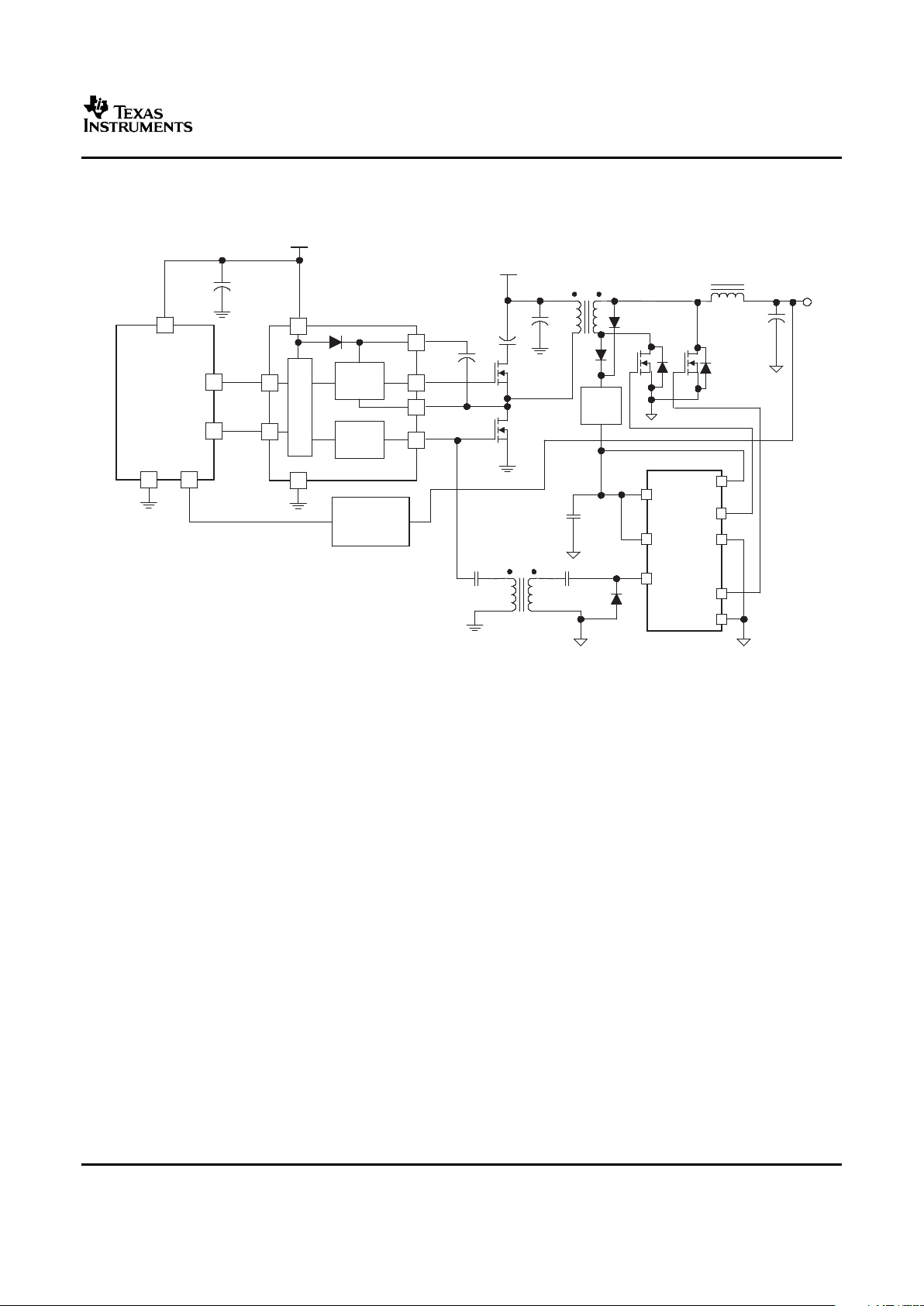
TYPICAL APPLICATIONS
3
3
2
BOOT
UGATE
PHASE
LGATE
GND
1
8
5
4
6
VDD
ENBL
7
PWM
3
OUT
FB
3
GND
3
TPS28225
V
DD
(4.5Vto8V)
V
IN
(3Vto32V − VDD)
V
OUT
VCC
TPS40200
TPS28225
SLUS710 – MAY 2006
One-Phase POL Regulator
2
Submit Documentation Feedback
www.ti.com
PWM
CONTROLLER
ISOLATION
AND
FEEDBACK
C O NT RO L
DRIVE
LO
DRIVE
HI
HI
LI
HB
HO
HS
LO
2
BOOT
UGATE
PHASE
LGATE
GND
1
8
5
4
3
VDD
EN/PG
7
PWM
6
LINEAR
REG.
VDD(4.5Vto8V)
V
OUT
=3.3V
35Vto75V
12V
PrimaryHighSide
V
DD
HighVoltageDriver
V
SS
TPS28255
TPS28225
SLUS710 – MAY 2006
TYPICAL APPLICATIONS (continued)
Driver for Synchronous Rectification with Complementary Driven MOSFETs
3
Submit Documentation Feedback
www.ti.com
5
4
7 3
8
1
2
2
BOOT
UGATE
PHASE
LGATE
GND
1
8
5
4
6 VDD
EN/PG
7
PWM
3
2
BOOT
UGATE
PHASE
LGATE
GND
1
8
5
4
6 VDD
EN
/PG
7
PWM
3
VIN
PWM 4
GND
VOUT
PWM1
8
PWM3
Enable
PWM2
ToDriver
ToDriver
GNDS
ToController
CSCNCS 4
ToController
CS 1
VDD(4.5Vto8V)
V
IN
(3Vto32V − VDD)
TPS28225
TPS28225
TPS4009x
oranyotheranalog
ordigitalcontroller
V
OUT
TPS28225
SLUS710 – MAY 2006
TYPICAL APPLICATIONS (continued)
Multi-Phase Synchronous Buck Converter
ORDERING INFORMATION
(1) (2) (3)
TEMPERATURE RANGE, TA= T
J
PACKAGE TAPE AND REEL QTY. PART NUMBER
Plastic 8-pin SOIC (D) 250 TPS28225DT
Plastic 8-pin SOIC (D) 2500 TPS28225DR
-40°C to 125°C
Plastic 8-pin DFN (DRB) 250 TPS28225DRBT
Plastic 8-pin DFN (DRB) 3000 TPS28225DRBR
(1) SOIC-8 (D) and DFN-8 (DRB) packages are available taped and reeled. Add T suffix to device type (e.g. TPS28225DT) to order taped
devices and suffix R to device type to order reeled devices.
(2) The SOIC-8 (D) and DFN-8 (DRB) package uses in Pb-Free lead finish of Pd-Ni-Au which is compatible with MSL level 1 at 255°C to
260°C peak reflow temperature to be compatible with either lead free or Sn/Pb soldering operations.
(3) In the DFN package, the pad underneath the center of the device is a thermal substrate. The PCB “thermal land” design for this
exposed die pad should include thermal vias that drop down and connect to one or more buried copper plane(s). This combination of
vias for vertical heat escape and buried planes for heat spreading allows the DFN to achieve its full thermal potential. This pad should
be either grounded for best noise immunity, and it should not be connected to other nodes.
4
Submit Documentation Feedback
www.ti.com
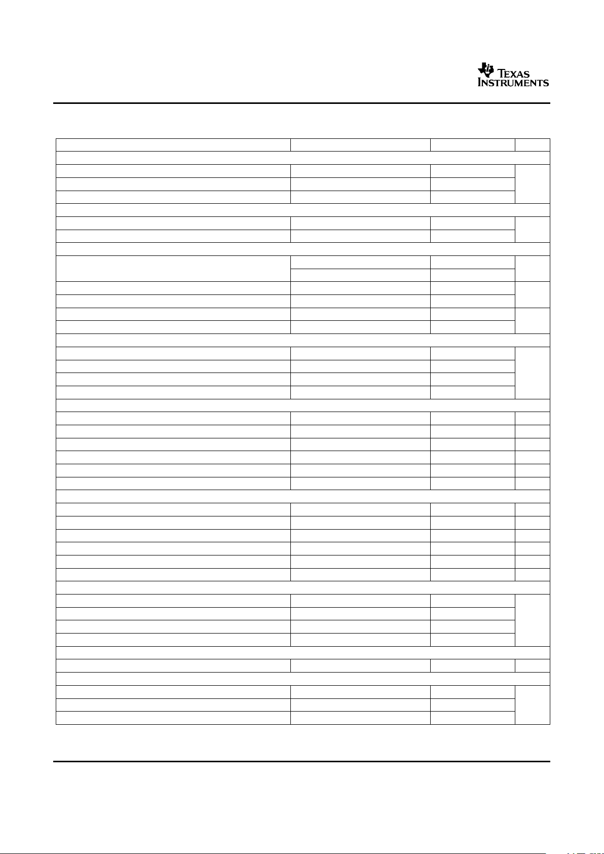
ABSOLUTE MAXIMUM RATINGS
DISSIPATION RATINGS
(1)
RECOMMENDED OPERATING CONDITIONS
TPS28225
SLUS710 – MAY 2006
over operating free-air temperature range (unless otherwise noted)
(1) (2)
TPS28225 VALUE UNIT
Input supply voltage range, V
DD
(3)
–0.3 to 8.8
Boot voltage, V
BOOT
–0.3 to 33
DC –2 to 32 or V
BOOT
+ 0.3 – V
DD
whichever is less
Phase voltage, V
PHASE
Pulse < 400 ns, E = 20 µ J –7 to 33.1 or V
BOOT
+ 0.3 – V
DD
whichever is less
Input voltage range, V
PWM
, V
EN/PG
–0.3 to 13.2
V
PHASE
– 0.3 to V
BOOT
+ 0.3, (V
BOOT
– V
PHASE
< 8.8) V
Output voltage range, V
UGATE
Pulse < 100 ns, E = 2 µ J V
PHASE
– 2 to V
BOOT
+ 0.3, (V
BOOT
– V
PHASE
< 8.8)
–0.3 to V
DD
+ 0.3
Output voltage range, V
LGATE
Pulse < 100 ns, E = 2 µ J –2 to V
DD
+ 0.3
ESD rating, HBM 2 k
ESD rating, HBM ESD rating, CDM 500
Continuous total power dissipation See Dissipation Rating Table
Operating virtual junction temperature range, T
J
–40 to 150
Operating ambient temperature range, T
A
–40 to 125
° C
Storage temperature, T
stg
–65 to 150
Lead temperature (soldering, 10 sec.) 300
(1) Stresses beyond those listed under “absolute maximum ratings” may cause permanent damage to the device. These are stress ratings
only, and functional operation of the device at these or any other conditions beyond those indicated under “recommended operating
conditions” is not implied. Exposure to absolute-maximum-rated conditions for extended periods may affect device reliability.
(2) These devices are sensitive to electrostatic discharge; follow proper device handling procedures.
(3) All voltages are with respect to GND unless otherwise noted. Currents are positive into, negative out of the specified terminal. Consult
Packaging Section of the Data book for thermal limitations and considerations of packages.
DERATING FACTOR TA< 25 ° C TA=70 ° C TA= 85 ° C
BOARD PACKAGE R
θ JC
R
θ JA
ABOVE TA= 25 ° C POWER RATING POWER RATING POWER RATING
High-K
(2)
D 39.4 ° C/W 100°C/W 10 mW/°C 1.25 W 0.8 W 0.65 W
High-K
(3)
DRB 1.4 ° C/W 48.5°C/W 20.6 mW/°C 2.58 W 1.65 W 1.34 W
(1) These thermal data are taken at standard JEDEC test conditions and are useful for the thermal performance comparison of different
packages. The cooling condition and thermal impedance R
θ JA
of practical design is specific.
(2) The JEDEC test board JESD51-7, 3-inch x 3-inch, 4-layer with 1-oz internal power and ground planes and 2-oz top and bottom trace
layers.
(3) The JEDEC test board JESD51-5 with direct thermal pad attach, 3-inch x 3-inch, 4-layer with 1-oz internal power and ground planes and
2-oz top and bottom trace layers.
over operating free-air temperature range (unless otherwise noted)
MIN TYP MAX UNIT
V
DD
Input supply voltage 4.5 7.2 8
V
V
IN
Power input voltage 3 32 V
–VDD
T
J
Operating junction temperature range –40 125 °C
5
Submit Documentation Feedback
www.ti.com
ELECTRICAL CHARACTERISTICS
(1)
TPS28225
SLUS710 – MAY 2006
V
DD
= 7.2 V, EN/PG pulled up to V
DD
by 100-k Ω resistor, TA= TJ= –40 ° C to 125 ° C (unless otherwise noted)
PARAMETER TEST CONDITIONS MIN TYP MAX UNIT
UNDER VOLTAGE LOCKOUT
Rising threshold V
PWM
= 0 V 3.2 3.5 3.8
Falling threshold V
PWM
= 0 V 2.7 3.0 V
Hysteresis 0.5
BIAS CURRENTS
I
DD(off)
Bias supply current V
EN/PG
= low, PWM pin floating 350
µ A
I
DD
Bias supply current V
EN/PG
= high, PWM pin floating 500
INPUT (PWM)
V
PWM
= 5 V 185
I
PWM
Input current µ A
V
PWM
= 0 V –200
PWM 3-state rising threshold
(2)
1.0
V
PWM 3-state falling threshold V
PWM
PEAK = 5 V 3.4 3.8 4.0
t
HLD_R
3-state shutdown Hold-off time 250
ns
T
MIN
PWM minimum pulse to force U
GATE
pulse CL= 3 nF at U
GATE
, V
PWM
= 5 V 30
ENABLE/POWER GOOD (EN/PG)
Enable high rising threshold PG FET OFF 1.7 2.1
Enable low falling threshold PG FET OFF 0.8 1.0
V
Hysteresis 0.35 0.70
Power good output V
DD
= 2.5 V 0.2
UPPER GATE DRIVER OUTPUT (UGATE)
Source resistance 500 mA source current 1.0 2.0 Ω
Source current
(2)
V
UGATE-PHASE
= 2.5 V 2.0 A
t
RU
Rise time CL= 3 nF 10 ns
Sink resistance 500 mA sink current 1.0 2.0 Ω
Sink current
(2)
V
UGATE-PHASE
= 2.5 V 2.0 A
t
FU
Fall time CL= 3 nF 10 ns
LOWER GATE DRIVER OUTPUT (LGATE)
Source resistance 500 mA source current 1.0 2.0 Ω
Source current
(2)
V
LGATE
= 2.5 V 2.0 A
t
RL
Rise time
(2)
CL= 3 nF 10 ns
Sink resistance 500 mA sink current 0.4 1.0 Ω
Sink current
(2)
V
LGATE
= 2.5 V 4.0 A
Fall time
(2)
CL= 3 nF 5 ns
SWITCHING TIME
t
DLU
UGATE turn-off propagation Delay CL= 3 nF 14
t
DLL
LGATE turn-off propagation Delay CL= 3 nF 14
ns
t
DTU
Dead time LGATE turn-off to UGATE turn-on CL= 3 nF 14
t
DTL
Dead time UGATE turn-off to LGATE turn-on CL= 3 nF 14
BOOTSTRAP DIODE
V
F
Forward voltage Forward bias current 100 mA 1.0 V
THERMAL SHUTDOWN
Rising threshold
(2)
150 160 170
Falling threshold
(2)
130 140 150 ° C
Hysteresis 20
(1) Typical values for TA= 25°C
(2) Not tested in production
6
Submit Documentation Feedback

www.ti.com
DEVICE INFORMATION
1
2
3
4
8
7
6
5
UGATE
BOOT
PWM
GND
PHASE
EN/PG
VDD
LGATE
5
3
7
6
81
2BOOT
PWM VDD
EN/PG
LG ATEGND
UG ATE PHASE
4
Exposed
Thermal
Die Pad
6
13K
2
VDD
EN /PG
BOOT
UGATE
PHASE
LGATE
GND
7
1
8
5
4
VDD
27K
3−STATE
INPUT
CIRCUIT
PWM
3
SHOOT −
THROUGH
PROTECTION
THERMAL
SD
HLD−OFF
TIME
UVLO
TPS28225
SLUS710 – MAY 2006
SOIC-8 Package (top view)
DRB-8 Package (top view)
FUNCTIONAL BLOCK DIAGRAM
A. For the TPS28224DRB device the thermal PAD on the bottom side of package must be soldered and connected to
the GND pin and to the GND plane of the PCB in the shortest possible way. See Recommended Land Pattern in the
Application section.
7
Submit Documentation Feedback
www.ti.com
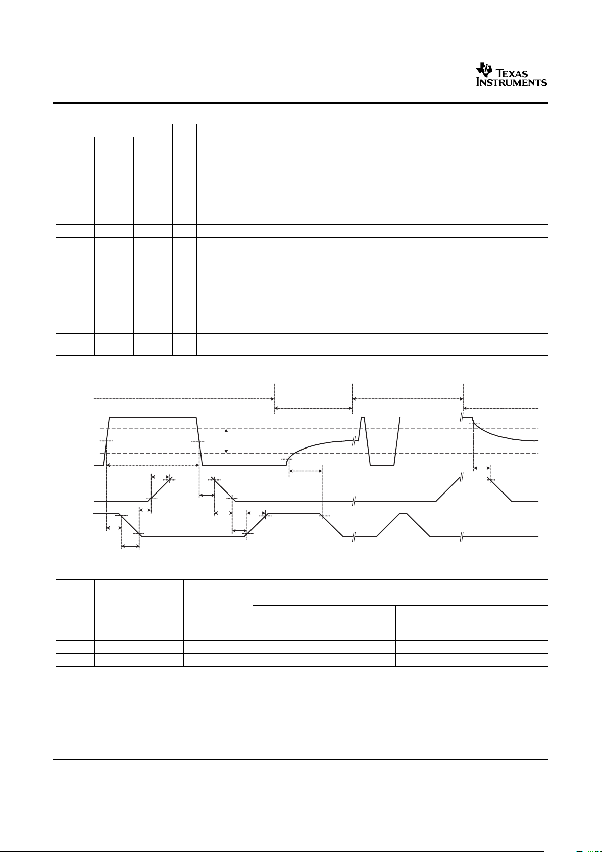
Normal switching
PWM
LGATE
UGATE
3 −State
window
90 %
10 %
t
DLL
50 %
t
FL
50 %
t
PWM_MIN
t
DTU
90 %
10 %
t
RU
90 %
10 %
t
DLU
t
FU
t
DTL
90 %
10 %
t
RL
t
HLD_R
90 %
10 %
90 %
90 %
t
HLD_F
Enter into 3 −State
at PWM rise
Exit 3 −State
Enter into 3 −State
at PWM fall
PWM Low and High after 3 −
State to allow Bootstrap
Capacitor Restore Charge
TRUTH TABLE
TPS28225
SLUS710 – MAY 2006
TERMINAL FUNCTIONS
TERMINAL
I/O DESCRIPTION
SOIC-8 DRB-8 NAME
1 1 UGATE O Upper gate drive sink/source output. Connect to gate of high-side power N-Channel MOSFET.
Floating bootstrap supply pin for the upper gate drive. Connect the bootstrap capacitor between
2 2 BOOT I/O this pin and the PHASE pin. The bootstrap capacitor provides the charge to turn on the upper
MOSFET.
The PWM signal is the control input for the driver. The PWM signal can enter three distinct states
3 3 PWM I during operation, see the 3-state PWM Input section under DETAILED DESCRIPTION for further
details. Connect this pin to the PWM output of the controller.
4 4 GND — Ground pin. All signals are referenced to this node.
Exposed Thermal
— Connect directly to the GND for better thermal performance and EMI
die pad pad
Lower gate drive sink/source output. Connect to the gate of the low-side power N-Channel
5 5 LGATE O
MOSFET.
6 6 VDD I Connect this pin to a 5-V bias supply. Place a high quality bypass capacitor from this pin to GND.
Enable/Power Good input/output pin with 1M Ω impedance. Connect this pin to HIGH to enable
and LOW to disable the IC. When disabled, the device draws less than 350 µ A bias current. If the
7 7 EN/PG I/O
V
DD
is below UVLO threshold or over temperature shutdown occurs, this pin is internally pulled
low.
Connect this pin to the source of the upper MOSFET and the drain of the lower MOSFET. This pin
8 8 PHASE I
provides a return path for the upper gate driver.
TIMING DIAGRAM
V
DD
FALLING > 3 V AND TJ< 150 ° C
V
DD
RISING < 3.5 V EN/PG FALLING > 1.0 V
PIN
EN/PG RISING
OR TJ> 160 ° C
PWM > 1.5 V AND PWM SIGNAL SOURCE IMPEDANCE
< 1.7 V
PWM < 1 V
T
RISE
/T
FALL
< 200 ns >40 k Ω FOR > 250ns (3-State)
(1)
LGATE Low Low High Low Low
UGATE Low Low Low High Low
EN/PG Low
(1) To exit the 3-state condition, the PWM signal should go low. One Low PWM input signal followed by one High PWM input signal is
required before re-entering the 3-state condition.
8
Submit Documentation Feedback
www.ti.com
TYPICAL CHARACTERISTICS
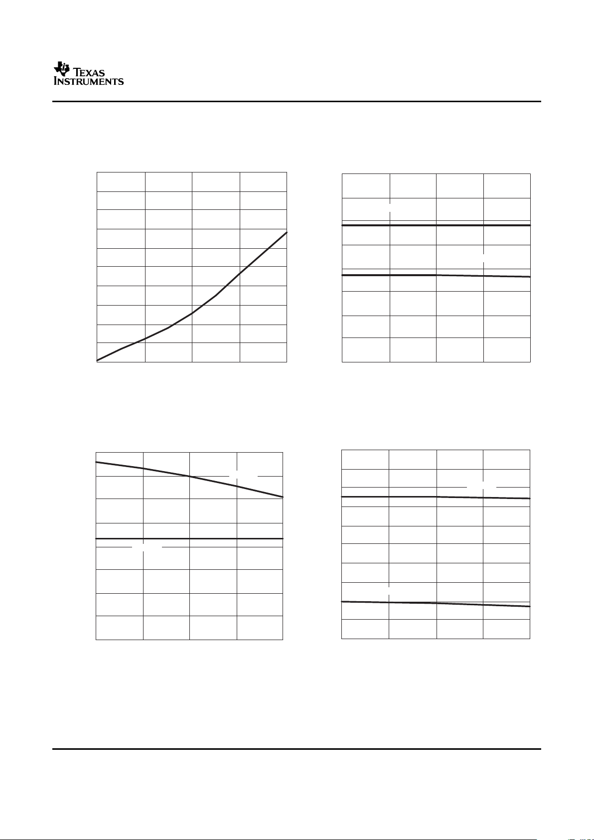
−40 125
300
340
380
420
460
500
25
320
360
400
440
480
TJ − Temperature − °C
I
DD(off)
− Bias Supply − µA
2.00
2.75
3.25
4.00
2.25
2.50
3.00
3.50
3.75
UVLO − Under Voltage Lockout − V
−40 12525
Falling
Rising
TJ − Temperature − °C
0.0
PWM − PWM 3−State Threshold − V
−40 12525
2.0
3.0
5.0
0.5
1.0
2.5
2.5
4.5
1.5
4.0
Falling
Rising
TJ − Temperature − °C
−40 12525
0.00
0.75
1.25
2.00
0.25
0.50
1.00
1.50
1.75
Falling
Rising
TJ − Temperature − °C
EN/PG − Enable/Power Good − V
TPS28225
SLUS710 – MAY 2006
BIAS SUPPLY CURRENT UNDER VOLTAGE LOCKOUT THRESHOLD
vs vs
TEMPERATURE TEMPERATURE
(V
EN/PG
= Low, PWM Input Floating, V
DD
= 7.2V)
Figure 1. Figure 2.
ENABLE/POWER GOOD THRESHOLD PWM 3-STATE THRESHOLDS, (5-V Input Pulses)
vs vs
TEMPERATURE (V
DD
= 7.2 V) TEMPERATURE, (V
DD
= 7.2 V)
Figure 3. Figure 4.
9
Submit Documentation Feedback
www.ti.com
0
−40 12525
0.75
1.25
2.00
0.25
0.50
1.00
1.50
1.75
R
SINK
R
SOURCE
TJ − Temperature − °C
R
OUT
− Output Impedance − Ω
0
−40 12525
0.75
1.25
2.00
0.25
0.50
1.00
1.50
1.75
R
SINK
R
SOURCE
TJ − Temperature − °C
R
OUT
− Output Impedance − Ω
−40 12525
4
6
10
12
14
5
7
9
11
13
8
Falling
Rising
TJ − Temperature − °C
t
RL
/t
FL
− Rise and Fall Time − ns
6
8
11
13
15
7
9
10
12
14
−40 12525
Falling
Rising
TJ − Temperature − °C
t
RU
/t
FU
− Rise and Fall Time − ns
TPS28225
SLUS710 – MAY 2006
TYPICAL CHARACTERISTICS (continued)
UGATE DC OUTPUT IMPEDANCE LGATE DC OUTPUT IMPEDANCE
vs vs
TEMPERATURE, (V
DD
= 7.2 V) TEMPERATURE (V
DD
= 7.2 V)
Figure 5. Figure 6.
UGATE RISE AND FALL TIME LGATE RISE AND FALL TIME
vs vs
TEMPERATURE (V
DD
= 7.2 V, C
LOAD
= 3 nF) TEMPERATURE (V
DD
= 7.2 V, C
LOAD
= 3 nF)
Figure 7. Figure 8.
10
Submit Documentation Feedback

www.ti.com
0
20
25
30
5
10
15
−40 12525
L
GATE
U
GATE
TJ − Temperature − °C
t
DLU
/t
DLL
− U
GATE
and L
GATE
− ns
−40 12525
0.0
12.5
17.5
20.0
2.5
7.5
10.0
5.0
15.0
L
GATE
U
GATE
TJ − Temperature − °C
t
DTU
/t
DTL
− U
GATE
and L
GATE
− ns
0.5
0.8
1.0
1.3
0.6
0.7
0.9
1.1
1.2
−40 12525
TJ − Temperature − °C
V
F
− Forward Voltage − V
0
5
25
30
10
15
20
−40 12525
TJ − Temperature − °C
T
MIN
− Minimum Short Pulse − ns
TPS28225
SLUS710 – MAY 2006
TYPICAL CHARACTERISTICS (continued)
UGATE AND LGATE (Turning OFF Propagation Delays) UGATE AND LGATE (Dead Time)
vs vs
TEMPERTURE (V
DD
= 7.2 V, C
LOAD
= 3 nF) TEMPERTURE (V
DD
= 7.2 V, C
LOAD
= 3 nF)
Figure 9. Figure 10.
UGATE MINIMUM SHORT PULSE BOOTSTRAP DIODE FORWARD VOLTAGE
vs vs
TEMPERATURE (V
DD
= 7.2 V, C
LOAD
= 3 nF) TEMPERATURE (V
DD
= 7.2 V, IF= 100 mA)
Figure 11. Figure 12.
11
Submit Documentation Feedback

www.ti.com
0
200
1000
1200
400
600
800
100 300 500 700 1500 1700900 1100 19001300
UG = 50 nC
LG = 50 nC
UG = 25 nC
LG = 50 nC
UG = 25 nC
LG = 100 nC
FSW − Switching Frequency − kHz
P
DISS
− Dissipated Power − mW
0
15
5
10
100 300 500 700 1500 1700900 1100 19001300
FSW − Switching Frequency − kHz
I
DD
− Bias Supply Current − mA
PWM
UGATE
LGATE
VDD = 7.2 V , CL = 3 nF, TJ = 25°C
t − Time − 10 ns/div .
Voltage − 5 V/div.
PWM
UGATE
LGATE
VDD = 7.2 V , CL = 3 nF, TJ = 25°C
t − Time − 10 ns/div .
Voltage − 5 V/div.
TPS28225
SLUS710 – MAY 2006
TYPICAL CHARACTERISTICS (continued)
BIAS SUPPLY CURRENT DRIVER DISSIPATED POWER
vs vs
SWITCHING FREQUENCY SWITCHING FREQUENCY
(V
DD
= 7.2 V, No Load, TJ= 25 ° C) (Different Load Charge, V
DD
= 7.2 V, TJ= 25 ° C)
Figure 13. Figure 14.
PWM INPUT RISING SWITCHING WAVEFORMS PWM INPUT FALLING SWITCHING WAVEFORMS
Figure 15. Figure 16.
12
Submit Documentation Feedback

www.ti.com
PWM 30ns
UGATE
LGATE
VDD = 7.2 V , CL = 3 nF, TJ = 25°C
t − Time − 20 ns/div .
Voltage − 5 V/div.
PWM − 2 V/div.
3−St Trigger, High = 3−St
UGATE − 10 V/div.
LGATE − 10 V/div.
Voltage
t − Time − 5 µs/div.
TPS28225
SLUS710 – MAY 2006
TYPICAL CHARACTERISTICS (continued)
MINIMUM UGATE PULSE SWITCHING WAVEFORMS NORMAL AND 3-STATE OPERATION
ENTER/EXIT CONDITIONS
Figure 17. Figure 18.
13
Submit Documentation Feedback

www.ti.com
DETAILED DESCRIPTION
UNDER VOLTAGE LOCKOUT (UVLO)
OUTPUT ACTIVE LOW
ENABLE/POWER GOOD
Thermal SD
UVLO
7
EN/PG
6
System
Controller
. 20 kΩ
V
CC
VDD = 4.5 V to 8 V
Driver TPS28225
1 kΩ
1 M
R
DS(on)
= 1 kΩ
2 V Rise
1 V Fall
TPS28225
SLUS710 – MAY 2006
The TPS28225 incorporates an under voltage lockout circuit that keeps the driver disabled and external power
FETs in an OFF state when the input supply voltage V
DD
is insufficient to drive external power FETs reliably.
During power up, both gate drive outputs remain low until voltage V
DD
reaches UVLO threshold, typically 3.5V.
Once the UVLO threshold is reached, the condition of gate drive outputs is defined by the input PWM and
EN/PG signals. During power down the UVLO threshold is set lower, typically 3.0V. The 0.5-V hysteresis is
selected to prevent the driver from turning ON and OFF while the input voltage crosses UVLO thresholds,
especially with low slew rate. The TPS28225 has the ability to send a signal back to the system controller that
the input supply voltage V
DD
is insufficient by internally pulling down the EN/PG pin. The TPS28225 releases
EN/PG pin immediately after the V
DD
has risen above the UVLO threshold.
The output active low circuit effectively keeps the gate outputs low even if the driver is not powered up. This
prevents open gate conditions on the external power FETs and accidental turn ON when the main power stage
supply voltage is applied before the driver is powered up. For the simplicity, the output active low circuit is
shown in a block diagram as the resistor connected between LGATE and GND pins with another one connected
between UGATE and PHASE pins.
The Enable/Power Good circuit allows the TPS28225 to follow the PWM input signal when the voltage at EN/PG
pin is above 2.1 V maximum. This circuit has a unique two-way communication capability. This is illustrated by
Figure 19 .
Figure 19. Enable/Power Good Circuit
The EN/PG pin has approximately 1-k Ω internal series resistor. Pulling EN/PG high by an external ≥ 20-k Ω
resistor allows two-way communication between controller and driver. If the input voltage V
DD
is below UVLO
threshold or thermal shut down occurs, the internal MOSFET pulls EN/PG pin to GND through 1-k Ω resistor.
The voltage across the EN/PG pin is now defined by the resistor divider comprised by the external pull up
resistor, 1-k Ω internal resistor and the internal FET having 1k Ω R
DS(on)
. Even if the system controller allows the
driver to start by setting its own enable output transistor OFF, the driver keeps the voltage at EN/PG low. Low
EN/PG signal indicates that the driver is not ready yet because the supply voltage V
DD
is low or that the driver is
in thermal shutdown mode. The system controller can arrange the delay of PWM input signals coming to the
driver until the driver releases EN/PG pin. If the input voltage V
DD
is back to normal, or the driver is cooled down
below its lower thermal shutdown threshold, then the internal MOSFET releases the EN/PG pin and normal
operation resumes under the external Enable signal applied to EN/PG input. Another feature includes an internal
1M Ω resistor that pulls EN/PG pin low and disables the driver in case the system controller accidentally loses
connection with the driver. This could happen if, for example, the system controller is located on a separate PCB
daughter board.
14
Submit Documentation Feedback

www.ti.com
3-STATE INPUT
TPS28225
SLUS710 – MAY 2006
DETAILED DESCRIPTION (continued)
The EN/PG pin can serve as the second pulse input of the driver additionally to PWM input. The delay between
EN/PG and the UGATE going high, provided that PWM input is also high, is only about 30ns. If the PWM input
pulses are synchronized with EN/PG input, then when PWM and EN/PG are high, the UGATE is high and
LGATE is low. If both PWM and EN/PG are low, then UGATE and LGATE are both low as well. This means the
driver allows operation of a synchronous buck regulator as a convertional buck regulator using the body diode of
the low side power MOSFET as the freewheeling diode. This feature can be useful in some specific applications
to allow startup with a pre-biased output or, to improve the efficiency of buck regulator when in power saving
mode with low output current.
As soon as the EN/PG pin is set high and input PWM pulses are initiated (see 1 below
(1)
). The dead-time control
circuit ensures that there is no overlapping between UGATE and LGATE drive outputs to eliminate shoot
through current through the external power FETs. Additionally to operate under periodical pulse sequencing, the
TPS28225 has a self-adjustable PWM 3-state input circuit. The 3-state circuit sets both gate drive outputs low,
and thus turns the external power FETs OFF if the input signal is in a high impedance state for at least 250 ns
typical. At this condition, the PWM input voltage level is defined by the internal 27k Ω to 13k Ω resistor divider
shown in the block diagram. This resistor divider forces the input voltage to move into the 3-state window.
Initially the 3-state window is set between 1.0-V and 2.0-V thresholds. The lower threshold of the 3-state window
is always fixed at about 1.0 V. The higher threshold is adjusted to about 75% of the input signal amplitude. The
self-adjustable upper threshold allows shorter delay if the input signal enters the 3-state window while the input
signal was high, thus keeping the high-side power FET in ON state just slightly longer then 250 ns time constant
set by an internal 3-state timer. Both modes of operation, PWM input pulse sequencing and at the 3-state
condition, are illustrated in the timing diagrams shown in Figure 18 . The self-adjustable upper threshold allows
operation in wide range amplitude of input PWM pulse signals. The waveforms in Figure 20 and Figure 21
illustrate operation at normal and 3-state mode with the input pulse amplitudes 6 V and 2.5 V accordingly. After
entering into the 3-state window and staying within the window for the hold-off time, the PWM input signal level
is defined by the internal resistor divider and, depending on the input pulse amplitude, can be pulled up above
the normal PWM pulse amplitude (Figure 21 ) or down below the normal input PWM pulse (Figure 20 ). To exit
from the 3-state operation mode, the input signal should go low and then high at least once. This is necessary to
restore the voltage across the bootstrap capacitor that could be discharged during the 3-state mode if the 3-state
condition lasts long enough.
Figure 20. 6-V Amplitude PWM Pulse Figure 21. 2.5-V Amplitude PWM Pulse
(1) The driver sets UGATE low and LGATE high when PWM is low. When the PWM goes high, UGATE goes high and LGATE goes low.
15
Submit Documentation Feedback

www.ti.com
TPS28225
SLUS710 – MAY 2006
DETAILED DESCRIPTION (continued)
IMPORTANT NOTE: Any external resistor between PWM input and GND with the value lower than 40k Ω can
interfere with the 3-state thresholds. If the driver is intended to operate in the 3-state mode, any resistor below
40k Ω at the PWM and GND should be avoided. A resistor lower than 3.5k Ω connected between the PWM and
GND completely disables the 3-state function. In such case, the 3-state window shrinks to zero and the lower
3-state threshold becomes the boundary between the UGATE staying low and LGATE being high and vice versa
depending on the PWM input signal applied. It is not necessary to use a resistor <3.5k Ω to avoid the 3-state
condition while using a controller that is 3-state capable. If the rise and fall time of the input PWM signal is
shorter than 250ns, then the driver never enter into the 3-state mode.
In the case where the low-side MOSFET of a buck converter stays on during shutdown, the 3-state feature can
be fused to avoid negative resonent voltage across the output capacitor. This feature also can be used during
start up with a pre-biased output in the case where pulling the output low during the startup is not allowed due to
system requirements. If the system controller does not have the 3-state feature and never goes into the
high-impedance state, then setting the EN/PG signal low will keep both gate drive outputs low and turn both lowand high-side MOSFETs OFF during the shut down and start up with the pre-biased output.
The self-adjustable input circuit accepts wide range of input pulse amplitudes (2V up to 13.2V) allowing use of a
variety of controllers with different outputs including logic level. The wide PWM input voltage allows some
flexibility if the driver is used in secondary side synchronous rectifier circuit. The operation of the TPS28225 with
a 12-V input PWM pulse amplitude, and with V
DD
= 7.2V and V
DD
= 5V respectively is shown in Figure 22 and
Figure 23 .
Figure 22. 12-V PWM Pulse at V
DD
= 7.2 V Figure 23. 12-V PWM Pulse at V
DD
= 5 V
16
Submit Documentation Feedback

www.ti.com
BOOTSTRAP DIODE
UPPER AND LOWER GATE DRIVERS
DEAD TIME CONTROL
THERMAL SHUTDOWN
TPS28225
SLUS710 – MAY 2006
DETAILED DESCRIPTION (continued)
The bootstrap diode provides the supply voltage for the UGATE driver by charging the bootstrap capacitor
connected between BOOT and PHASE pins from the input voltage VDD when the low-side FET is in ON state.
At the very initial stage when both power FETs are OFF, the bootstrap capacitor is pre-charged through this
path including the PHASE pin, output inductor and large output capacitor down to GND. The forward voltage
drop across the diode is only 1.0V at bias current 100 mA. This allows quick charge restore of the bootstrap
capacitor during the high-frequency operation.
The upper and lower gate drivers charge and discharge the input capacitance of the power MOSFETs to allow
operation at switching frequencies up to 2 MHz. The output stage consists of a P-channel MOSFET providing
source output current and an N-channel MOSFET providing sink current through the output stage. The ON state
resistances of these MOSFETs are optimized for the synchronous buck converter configuration working with low
duty cycle at the nominal steady state condition. The UGATE output driver is capable of propagating PWM input
puses of less than 30-ns while still maintaining proper dead time to avoid any shoot through current conditions.
The waveforms related to the narrow input PWM pulse operation are shown in Figure 17 .
The dead-time control circuit is critical for highest efficiency and no shoot through current operation througout
the whole duty cycle range with the different power MOSFETs. By sensing the output of driver going low, this
circuit does not allow the gate drive output of another driver to go high until the first driver output falls below the
specified threshold. This approach to control the dead time is called adaptive. The overall dead time also
includes the fixed portion to ensure that overlapping never exists. The typical dead time is around 14 ns,
although it varies over the driver internal tolerances, layout and external MOSFET parasitic inductances. The
proper dead time is maintained whenever the current through the output inductor of the power stage flows in the
forward or reverse direction. Reverse current could happen in a buck configuration during the transients or while
dynamically changing the output voltage on the fly, as some microprocessors require. Because the dead time
does not depend on inductor current direction, this driver can be used both in buck and boost regulators or in
any bridge configuration where the power MOSFETs are switching in a complementary manner. Keeping the
dead time at short optimal level boosts efficiency by 1% to 2% depending on the switching frequency. Measured
switching waveforms in one of the practical designs show 10-ns dead time for the rising edge of PHASE node
and 22 ns for the falling edge (Figure 29 and Figure 30 in the Application Section of the data sheet).
Large non-optimal dead time can cause duty cycle modulation of the dc-to-dc converter during the operation
point where the output inductor current changes its direction right before the turn ON of the high-side MOSFET.
This modulation can interfere with the controller operation and it impacts the power stage frequency response
transfer function. As the result, some output ripple increase can be observed. The TPS28225 driver is designed
with the short adaptive dead time having fixed delay portion that eliminates risk of the effective duty cycle
modulation at the described boundary condition.
If the junction temperature exceeds 160 ° C, the thermal shutdown circuit will pull both gate driver outputs low and
thus turning both, low-side and high-side power FETs OFF. When the driver cools down below 140 ° C after a
thermal shutdown, then it resumes its normal operation and follows the PWM input and EN/PG signals from the
external control circuit. While in thermal shutdown state, the internal MOSFET pulls the EN/PG pin low, thus
setting a flag indicating the driver is not ready to continue normal operation. Normally the driver is located close
to the MOSFETs, and this is usually the hottest spots on the PCB. Thus, the thermal shutdown feature of
TPS28225 can be used as an additional protection for the whole system from overheating.
17
Submit Documentation Feedback

www.ti.com
APPLICATION INFORMATION
SWITCHING THE MOSFETs
4
5
GND
6
VDD
LGATE
Cvdd
L bondwire
Rsink
Rsource
L pin
L trace
L bondwire
L bondwire
Driver
Output
Stage
L pin
L pin
L trace
Isink
L trace
Cgs
Rg
L trace
Isource
TPS28225
SLUS710 – MAY 2006
Driving the MOSFETs efficiently at high switching frequencies requires special attention to layout and the
reduction of parasitic inductances. Efforts need to be done both at the driver’s die and package level and at the
PCB layout level to keep the parasitic inductances as low as possible. Figure 24 shows the main parasitic
inductances and current flow during turning ON and OFF of the MOSFET by charging its C
GS
gate capacitance.
Figure 24. MOSFET Drive Paths and Main Circuit Parasitics
18
Submit Documentation Feedback

www.ti.com
Voltage
Current
t − Time − ns
LGATE Falling, V or A
LGATE Falling, V or A
LGATE Current, A
Voltage
Current
t − Time − ns
UGATE Falling, V
UGATE Falling, V
UGATE Current, A
TPS28225
SLUS710 – MAY 2006
APPLICATION INFORMATION (continued)
The I
SOURCE
current charges the gate capacitor and the I
SINK
current discharges it. The rise and fall time of
voltage across the gate defines how quickly the MOSFET can be switched. The timing parameters specified in
datasheet for both upper and lower driver are shown in Figure 15 and Figure 16 where 3-nF load capacitor has
been used for the characterization data. Based on these actual measurements, the analytical curves in
Figure 25 and Figure 26 show the output voltage and current of upper and low side drivers during the
discharging of load capacitor. The left waveforms show the voltage and current as a function of time, while the
right waveforms show the relation between the voltage and current during fast switching. These waveforms
show the actual switching process and its limitations because of parasitic inductances. The static V
OUT
/ I
OUT
curves shown in many datasheets and specifications for the MOSFET drivers do not replicate actual switching
condition and provide limited information for the user.
Figure 25. LGATE Turning Off Voltage and Sink Current vs Time (Related Switching Diagram (right))
Figure 26. UGATE Turning Off Voltage and Sink Current vs Time (Related Switching Diagram (right)_
19
Submit Documentation Feedback

www.ti.com
Layout Recommendations
TPS28225
SLUS710 – MAY 2006
APPLICATION INFORMATION (continued)
Turning Off of the MOSFET needs to be done as fast as possible to reduce switching losses. For this reason the
TPS28225 driver has very low output impedance specified as 0.4 Ω typ for lower driver and 1 Ω typ for upper
driver at dc current. Assuming 8-V drive voltage and no parasitic inductances, one can expect an initial sink
current amplitude of 20A and 8A respectively for the lower and upper drivers. With pure R-C discharge circuit for
the gate capacitor, the voltage and current waveforms are expected to be exponential. However, because of
parasitic inductances, the actual waveforms have some ringing and the peak current for the lower driver is about
4A and about 2.5A for the upper driver (Figure 25 and Figure 26 ). The overall parasitic inductance for the lower
drive path is estimated as 4nH and for the upper drive path as 6nH. The internal parasitic inductance of the
driver, which includes inductances of bonded wires and package leads, can be estimated for SOIC-8 package
as 2nH for lower gate and 4nH for the upper gate. Use of DFN-8 package reduces the internal parasitic
inductances by approximately 50%.
To improve the switching characteristicsand efficiency of a design, the following layout rules need to be followed.
• Locate the driver as close as possible to the MOSFETs.
• Locate the V
DD
and bootstrap capacitors as close as possible to the driver.
• Pay special attention to the GND trace. Use the thermal pad of the DFN-8 package as the GND by
connecting it to the GND pin. The GND trace or pad from the driver goes directly to the source of the
MOSFET but should not include the high current path of the main current flowing through the drain and
source of the MOSFET.
• Use a similar rule for the PHASE node as for the GND.
• Use wide traces for UGATE and LGATE closely following the related PHASE and GND traces. Eighty to 100
mils width is preferable where possible.
• Use at least 2 or more vias if the MOSFET driving trace needs to be routed from one layer to another. For
the GND the number of vias are determined not only by the parasitic inductance but also by the
requirements for the thermal pad.
• Avoid PWM and enable traces going close to the PHASE node and pad where high dV/dT voltage can
induce significant noise into the relatively high impedance leads.
It should be taken into account that poor layout can cause 3% to 5% less efficiency versus a good layout design
and can even decrease the reliability of the whole system.
Figure 27. One of Phases Driven by TPS28225 Driver in 4-phase VRM Reference Design
20
Submit Documentation Feedback

www.ti.com
TPS28225
SLUS710 – MAY 2006
APPLICATION INFORMATION (continued)
The schematic of one of the phases in a multi-phase synchronous buck regulator and the related layout are
shown in Figure 27 and Figure 28 . These help to illustrate good design practices. The power stage includes one
high-side MOSFET Q10 and two low-side MOSFETS (Q8 and Q9). The driver (U7) is located on bottom side of
PCB close to the power MOSFETs. The related switching waveforms during turning ON and OFF of upper FET
are shown in Figure 29 and Figure 30 . The dead time during turning ON is only 10ns (Figure 29 ) and 22ns
during turning OFF (Figure 30 ).
Figure 28. Component Placement Based on Schematic in Figure 27
Figure 29. Phase Rising Edge Switching Waveforms (20ns/div) of the Power Stage in Figure 27
21
Submit Documentation Feedback

www.ti.com
LIST OF MATERIALS
TPS28225
SLUS710 – MAY 2006
APPLICATION INFORMATION (continued)
Figure 30. Phase Falling Edge Switching Waveforms (10ns/div) of the Power State in Figure 27
The list of materials for this specific example is provided in the table. The component vendors are not limited to
those shown in the table below. It should be notd that, in this example, the power MOSFET packages were
chosen with drains on top. The decoupling capacitors C47, C48, C65, and C66 were chosen to have low
profiles. This allows the designer to meet good layout rules and place a heatsink on top of the FETs using an
electrically isolated and thermally conductive pad.
List of Materials
REF DES COUNT DESCRIPTION MANUFACTURE PART NUMBER
C47, C48, 4 Capacitor, ceramic, 4.7 µ F, 16 V, X5R 10%, low profile 0.95 mm, 1206 TDK C3216X5R1C475K
C65, C66
C41, C42 2 Capacitor, ceramic, 10 µ F, 16 V, X7R 10%, 1206 TDK C3216X7R1C106K
C50, C51 2 Capacitor, ceramic, 1000 pF, 50 V, X7R, 10%, 0603 Std Std
C23 1 Capacitor, ceramic, 0.22 µ F, 16 V, X7R, 10%, 0603 Std Std
C25, C49, 3 Capacitor, ceramic, 1 µ F, 16 V, X7R, 10%, '0603 Std Std
C71
L3 1 Inductor, SMT, 0.12 µ H, 31 A, 0.36 m Ω , 0.400 x 0.276 Pulse PA0511-101
Q8, Q9 2 Mosfet, N-channel, VDS30 V, RDS2.4 m Ω , ID45 A, LFPAK-i Renesas RJK0301DPB-I
Q10 1 Mosfet, N-channel, VDS30 V, RDS6.2 m Ω , ID30 A, LFPAK-i Renesas RJK0305DPB-I
R32 1 Resistor, chip, 0 Ω , 1/10 W, 1%, '0805 Std Std
R51, R52 2 Resistor, chip, 2.2 Ω , 1/10 W, 1%, '0805 Std Std
U7 1 Device, High Frequency 4-A Sink Synchronous Buck MOSFET Driver, Texas Instruments TPS28225DRB
DFN-8
22
Submit Documentation Feedback

www.ti.com
EFFICIENCY OF POWER STAGE vs LOAD CURRENT AT DIFFERENT SWITCHING
TI: 400kHz
Ind: 400kHz
5 10 15 25 35
75
90
20 30
80
85
Efficiency − %
CL − Load Currnt − A
TI: 500kHz
Ind: 500kHz
5 10 15 25 35
75
90
20 30
80
85
Efficiency − %
CL − Load Currnt − A
TI: 600kHz
Ind: 600kHz
5 10 15 25 35
75
90
20 30
80
85
Efficiency − %
CL − Load Currnt − A
TPS28225
SLUS710 – MAY 2006
FREQUENCIES
Efficiency achieved using TPS28225 driver with 8-V drive at different switching frequencies a similar industry 5-V
driver using the power stage in Figure 27 is shown in Figure 33 , Figure 35 , Figure 34 , Figure 31 and Figure 32 .
EFFICIENCY EFFICIENCY
vs vs
LOAD CURRENT LOAD CURRENT
Figure 31. Figure 32.
EFFICIENCY
vs
LOAD CURRENT
Figure 33.
23
Submit Documentation Feedback

www.ti.com
TI: 700kHz
Ind: 700kHz
5 10 15 25 35
75
90
20 30
80
85
Efficiency − %
CL − Load Currnt − A
TI: 800kHz
Ind: 800kHz
5 10 15 25 35
75
90
20 30
80
85
Efficiency − %
CL − Load Currnt − A
Rdson @
Vg = 5V
Rdson @
Vg = 7V
Rdson @
Vg = 5V
Rdson @
Vg = 7V
400 500 700 800
0.0
1.5
2.0
600
0.5
1.0
DRIVE LOSS
vs
SWITCHING FREQUENCY
FSW − Switching Frequency − kHz
12−V
Estimation
SOIC−8
Package
Limit at 45°C
8−V
TPS28225
5−V
Ind. Std.
D
L
− Drive Loss − W
TPS28225
SLUS710 – MAY 2006
EFFICIENCY EFFICIENCY
vs vs
LOAD CURRENT LOAD CURRENT
Figure 34. Figure 35.
When using the same power stage, the driver with the optimal drive voltage and optimal dead time can boost
efficiency up to 5%. The optimal 8-V drive voltage versus 5-V drive contributes 2% to 3% efficiency increase and
the remaining 1% to 2% can be attributed to the reduced dead time. The 7-V to 8-V drive voltage is optimal for
operation at switching frequency range above 400kHz and can be illustrated by observing typical R
DS(on)
curves
of modern FETs as a function of their gate drive voltage. This is shown in Figure 36 .
Figure 36. R
DS(on)
of MOSFET as Function of V
GS
Figure 37. Drive Power as Function of V
GS
and F
SW
24
Submit Documentation Feedback

www.ti.com
RELATED PRODUCTS
TPS28225
SLUS710 – MAY 2006
The plots show that the R
DS(on)
at 5-V drive is substantially larger than at 7 V and above that the R
DS(on)
curve is
almost flat. This means that moving from 5-V drive to an 8-V drive boosts the efficiency because of lower R
DS(on)
of the MOSFETs at 8 V. Further increase of drive voltage from 8 V to 12 V only slightly decreases the
conduction losses but the power dissipated inside the driver increases dramatically (by 125%). The power
dissipated by the driver with 5V, 8V and 12V drive as a function of switching frequency from 400kHz to 800kHz.
It should be noted that the 12-V driver exceeds the maximum dissipated power allowed for an SOIC-8 package
even at 400-kHz switching frequency.
• TPS40090, 2/3/4-Phase Multi-Phase Controller
• TPS40091, 2/3/4-Phase Multi-Phase Controller
25
Submit Documentation Feedback

TAPE AND REEL INFORMATION
*All dimensions are nominal
Device Package
Type
Package
Drawing
Pins SPQ Reel
Diameter
(mm)
Reel
Width
W1 (mm)
A0 (mm) B0 (mm) K0 (mm) P1
(mm)W(mm)
Pin1
Quadrant
TPS28225DR SOIC D 8 2500 330.0 12.4 6.4 5.2 2.1 8.0 12.0 Q1
TPS28225DRBR SON DRB 8 3000 330.0 12.4 3.3 3.3 1.1 8.0 12.0 Q2
TPS28225DRBT SON DRB 8 250 180.0 12.4 3.3 3.3 1.1 8.0 12.0 Q2
PACKAGE MATERIALS INFORMATION
www.ti.com
19-Mar-2008
Pack Materials-Page 1

*All dimensions are nominal
Device Package Type Package Drawing Pins SPQ Length (mm) Width (mm) Height (mm)
TPS28225DR SOIC D 8 2500 340.5 338.1 20.6
TPS28225DRBR SON DRB 8 3000 346.0 346.0 29.0
TPS28225DRBT SON DRB 8 250 190.5 212.7 31.8
PACKAGE MATERIALS INFORMATION
www.ti.com
19-Mar-2008
Pack Materials-Page 2


IMPORTANT NOTICE
Texas Instruments Incorporated and its subsidiaries (TI) reserve the right to make corrections, modifications, enhancements, improvements,
and other changes to its products and services at any time and to discontinue any product or service without notice. Customers should
obtain the latest relevant information before placing orders and should verify that such information is current and complete. All products are
sold subject to TI’s terms and conditions of sale supplied at the time of order acknowledgment.
TI warrants performance of its hardware products to the specifications applicable at the time of sale in accordance with TI’s standard
warranty. Testing and other quality control techniques are used to the extent TI deems necessary to support this warranty. Except where
mandated by government requirements, testing of all parameters of each product is not necessarily performed.
TI assumes no liability for applications assistance or customer product design. Customers are responsible for their products and
applications using TI components. To minimize the risks associated with customer products and applications, customers should provide
adequate design and operating safeguards.
TI does not warrant or represent that any license, either express or implied, is granted under any TI patent right, copyright, mask work right,
or other TI intellectual property right relating to any combination, machine, or process in which TI products or services are used. Information
published by TI regarding third-party products or services does not constitute a license from TI to use such products or services or a
warranty or endorsement thereof. Use of such information may require a license from a third party under the patents or other intellectual
property of the third party, or a license from TI under the patents or other intellectual property of TI.
Reproduction of TI information in TI data books or data sheets is permissible only if reproduction is without alteration and is accompanied
by all associated warranties, conditions, limitations, and notices. Reproduction of this information with alteration is an unfair and deceptive
business practice. TI is not responsible or liable for such altered documentation. Information of third parties may be subject to additional
restrictions.
Resale of TI products or services with statements different from or beyond the parameters stated by TI for that product or service voids all
express and any implied warranties for the associated TI product or service and is an unfair and deceptive business practice. TI is not
responsible or liable for any such statements.
TI products are not authorized for use in safety-critical applications (such as life support) where a failure of the TI product would reasonably
be expected to cause severe personal injury or death, unless officers of the parties have executed an agreement specifically governing
such use. Buyers represent that they have all necessary expertise in the safety and regulatory ramifications of their applications, and
acknowledge and agree that they are solely responsible for all legal, regulatory and safety-related requirements concerning their products
and any use of TI products in such safety-critical applications, notwithstanding any applications-related information or support that may be
provided by TI. Further, Buyers must fully indemnify TI and its representatives against any damages arising out of the use of TI products in
such safety-critical applications.
TI products are neither designed nor intended for use in military/aerospace applications or environments unless the TI products are
specifically designated by TI as military-grade or "enhanced plastic." Only products designated by TI as military-grade meet military
specifications. Buyers acknowledge and agree that any such use of TI products which TI has not designated as military-grade is solely at
the Buyer's risk, and that they are solely responsible for compliance with all legal and regulatory requirements in connection with such use.
TI products are neither designed nor intended for use in automotive applications or environments unless the specific TI products are
designated by TI as compliant with ISO/TS 16949 requirements. Buyers acknowledge and agree that, if they use any non-designated
products in automotive applications, TI will not be responsible for any failure to meet such requirements.
Following are URLs where you can obtain information on other Texas Instruments products and application solutions:
Products Applications
Amplifiers amplifier.ti.com Audio www.ti.com/audio
Data Converters dataconverter.ti.com Automotive www.ti.com/automotive
DSP dsp.ti.com Broadband www.ti.com/broadband
Clocks and Timers www.ti.com/clocks Digital Control www.ti.com/digitalcontrol
Interface interface.ti.com Medical www.ti.com/medical
Logic logic.ti.com Military www.ti.com/military
Power Mgmt power.ti.com Optical Networking www.ti.com/opticalnetwork
Microcontrollers microcontroller.ti.com Security www.ti.com/security
RFID www.ti-rfid.com Telephony www.ti.com/telephony
RF/IF and ZigBee® Solutions www.ti.com/lprf Video & Imaging www.ti.com/video
Wireless www.ti.com/wireless
Mailing Address: Texas Instruments, Post Office Box 655303, Dallas, Texas 75265
Copyright © 2008, Texas Instruments Incorporated
 Loading...