

TPS2811, TPS2812, TPS2813, TPS2814, TPS2815
DUAL HIGH-SPEED MOSFET DRIVERS
SLVS132D – NOVEMBER 1995 – REVISED NOVEMBER 1997
1
POST OFFICE BOX 655303 • DALLAS, TEXAS 75265
D
Industry-Standard Driver Replacement
D
25-ns Max Rise/Fall Times and 40-ns Max
Propagation Delay – 1-nF Load, V
CC
= 14 V
D
2-A Peak Output Current, VCC = 14 V
D
5-µA Supply Current — Input High or Low
D
4-V to 14-V Supply-Voltage Range; Internal
Regulator Extends Range to 40 V (TPS2811,
TPS2812, TPS2813)
D
–40°C to 125°C Ambient-Temperature
Operating Range
description
The TPS28xx series of dual high-speed MOSFET
drivers are capable of delivering peak currents of
2 A into highly capacitive loads. This performance
is achieved with a design that inherently
minimizes shoot-through current and consumes
an order of magnitude less supply current than
competitive products.
The TPS2811, TPS2812, and TPS2813 drivers
include a regulator to allow operation with supply
inputs between 14 V and 40 V. The regulator
output can power other circuitry, provided power
dissipation does not exceed package limitations. When the regulator is not required, REG_IN and REG_OUT
can be left disconnected or both can be connected to V
CC
or GND.
The TPS2814 and the TPS2815 have 2-input gates that give the user greater flexibility in controlling the
MOSFET. The TPS2814 has AND input gates with one inverting input. The TPS2815 has dual-input NAND
gates.
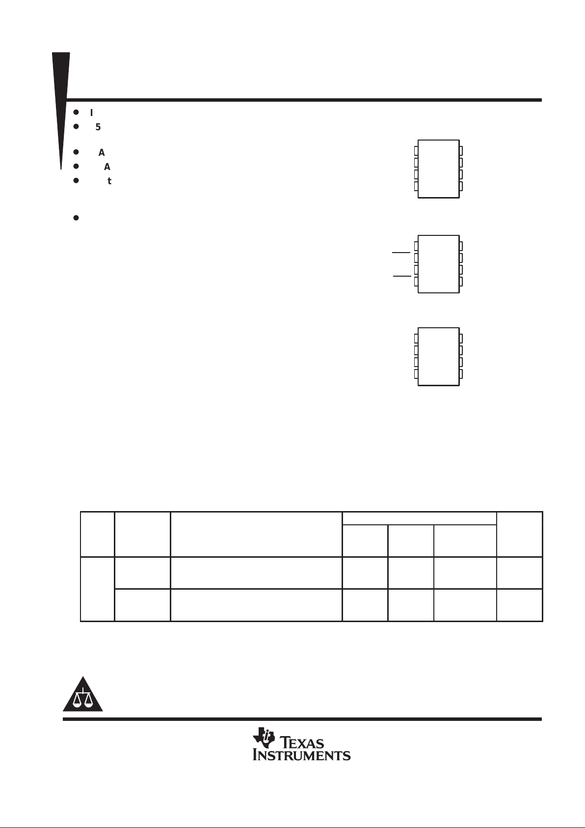
TPS28xx series drivers, available in 8-pin PDIP, SOIC, and TSSOP packages and as unmounted ICs, operate
over a ambient temperature range of –40°C to 125°C.
AVAILABLE OPTIONS
PACKAGED DEVICES
T
A
INTERNAL
REGULATOR
LOGIC FUNCTION
SMALL
OUTLINE
(D)
PLASTIC
DIP
(P)
TSSOP (PW)
CHIP
FORM
(Y)
–40°C
Yes
Dual inverting drivers
Dual noninverting drivers
One inverting and one noninverting driver
TPS2811D
TPS2812D
TPS2813D
TPS2811P
TPS2812P
TPS2813P
TPS2811PWLE
TPS2812PWLE
TPS2813PWLE
TPS2811Y
TPS2812Y
TPS2813Y
to
125°C
No
Dual 2-input AND drivers, one inverting input on
each driver
Dual 2-input NAND drivers
TPS2814D
TPS2815D
TPS2814P
TPS2815P
TPS2814PWLE
TPS2815PWLE
TPS2814Y
TPS2815Y
The D package is available taped and reeled. Add R suffix to device type (e.g., TPS281 1DR). The PW package is only available left-end
taped and reeled and is indicated by the LE suffix on the device type (e.g., TPS2811PWLE).
Please be aware that an important notice concerning availability, standard warranty, and use in critical applications of
Texas Instruments semiconductor products and disclaimers thereto appears at the end of this data sheet.
PRODUCTION DATA information is current as of publication date.
Products conform to specifications per the terms of Texas Instruments
standard warranty. Production processing does not necessarily include
testing of all parameters.
Copyright 1997, Texas Instruments Incorporated
1
2
3
4
8
7
6
5
REG_IN
1IN
GND
2IN
REG_OUT
1OUT
V
CC
2OUT
TPS2811, TPS2812, TPS2813 . . . D, P, AND PW
PACKAGES
(TOP VIEW)
1
2
3
4
8
7
6
5
1IN1
1IN2
2IN1
2IN2
GND
1OUT
V
CC
2OUT
TPS2814 . . . D, P, AND PW PACKAGES
(TOP VIEW)
1
2
3
4
8
7
6
5
1IN1
1IN2
2IN1
2IN2
GND
1OUT
V
CC
2OUT
TPS2815 . . . D, P, AND PW PACKAGES
(TOP VIEW)
TPS2811, TPS2812, TPS2813, TPS2814, TPS2815
DUAL HIGH-SPEED MOSFET DRIVERS
SLVS132D – NOVEMBER 1995 – REVISED NOVEMBER 1997
2
POST OFFICE BOX 655303 • DALLAS, TEXAS 75265
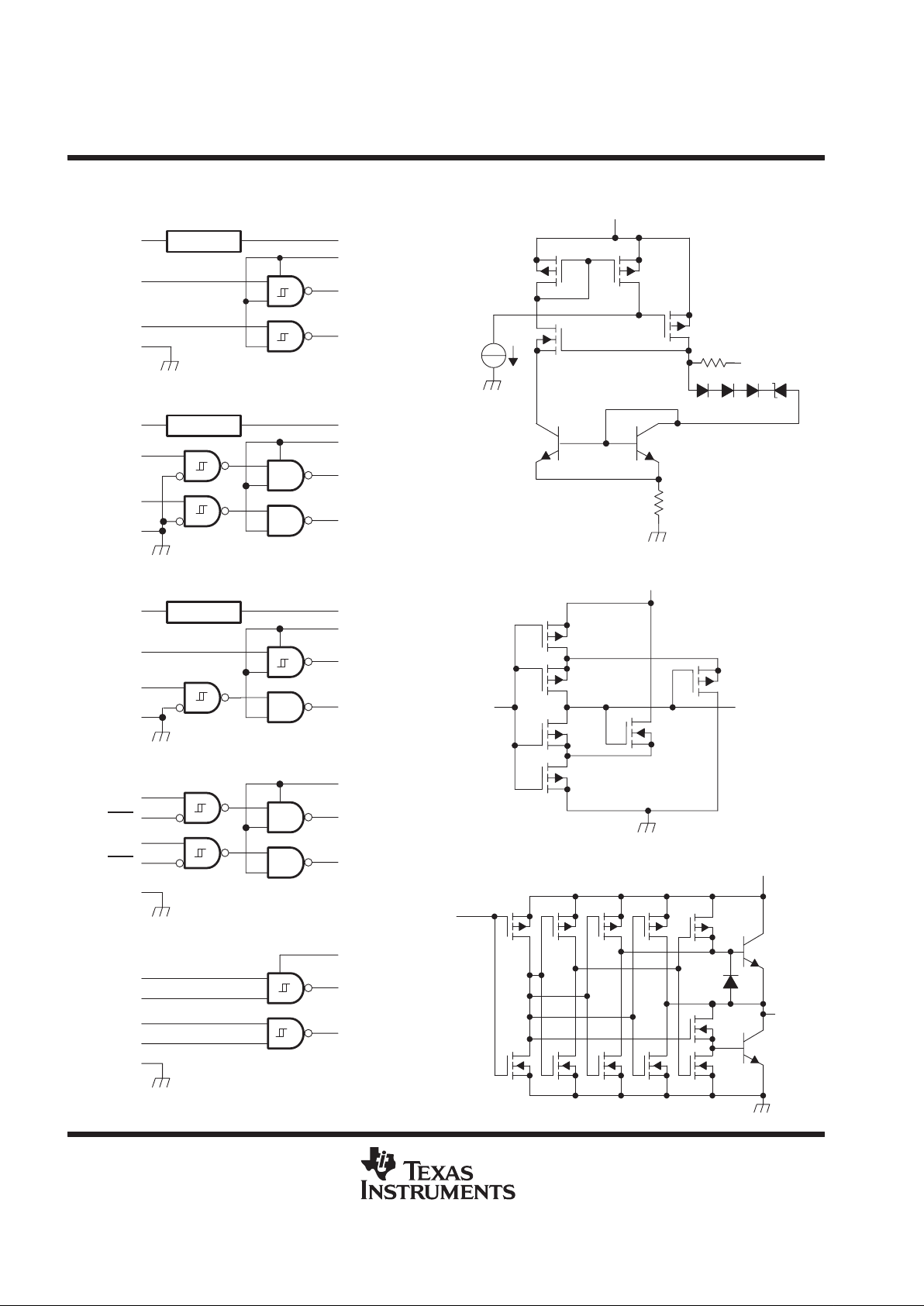
functional block diagram
Regulator
1
2
4
3
REG_IN
1IN
2IN
GND
8
6
7
5
REG_OUT
V
CC
1OUT
2OUT
TPS2811
Regulator
1
2
4
3
REG_IN
1IN
2IN
GND
8
6
7
5
REG_OUT
V
CC
1OUT
2OUT
TPS2812
Regulator
1
2
4
3
REG_IN
1IN
2IN
GND
8
6
7
5
REG_OUT
V
CC
1OUT
2OUT
TPS2813
1
3
8
1IN1
2IN1
GND
6
7
5
V
CC
1OUT
2OUT
TPS2814
2
4
1IN2
2IN2
1
3
8
1IN1
2IN1
GND
6
7
5
V
CC
1OUT
2OUT
TPS2815
2
4
1IN2
2IN2
REG_IN
7.5 Ω
REG_OUT
regulator diagram (TPS2811, TPS2812,
TPS2813 only)
input stage diagram
To Drive
Stage
IN
V
CC
output stage diagram
V
CC
OUT
Predrive
TPS2811, TPS2812, TPS2813, TPS2814, TPS2815
DUAL HIGH-SPEED MOSFET DRIVERS
SLVS132D – NOVEMBER 1995 – REVISED NOVEMBER 1997
3
POST OFFICE BOX 655303 • DALLAS, TEXAS 75265
TPS28xxY chip information
This chip, when properly assembled, displays characteristics similar to those of the TPS28xx. Thermal
compression or ultrasonic bonding may be used on the doped aluminum bonding pads. The chip may be
mounted with conductive epoxy or a gold-silicon preform.
57
BONDING PAD ASSIGNMENTS
CHIP THICKNESS: 15 MILS TYPICAL
BONDING PADS: 4 × 4 MILS MINIMUM
TJmax OPERATING TEMPERATURE = 150°C
TOLERANCES ARE ±10%.
ALL DIMENSIONS ARE IN MILS.
(7)
(6)
(1)
(5)
(2)
(3)
GND
1OUT
V
CC
REG_IN
1IN
TPS2811Y
TPS2812Y
TPS2813Y
REG_OUT
(8)
(4)
2IN
47
(1) (8)
(7)
(2)
(3)
(4)
(5)
(6)
2OUT
(6)
(5)
(1)
(4)
(2)
(8)
GND
1OUT
V
CC
1IN1
1IN2
TPS2814Y
(7)
(3)
2IN1
2OUT
2IN2
(6)
(5)
(1)
(4)
(2)
(8)
GND
1OUT
V
CC
1IN1
1IN2
TPS2815Y
(7)
(3)
2IN1
2OUT
2IN2
TPS2811, TPS2812, TPS2813, TPS2814, TPS2815
DUAL HIGH-SPEED MOSFET DRIVERS
SLVS132D – NOVEMBER 1995 – REVISED NOVEMBER 1997
4
POST OFFICE BOX 655303 • DALLAS, TEXAS 75265
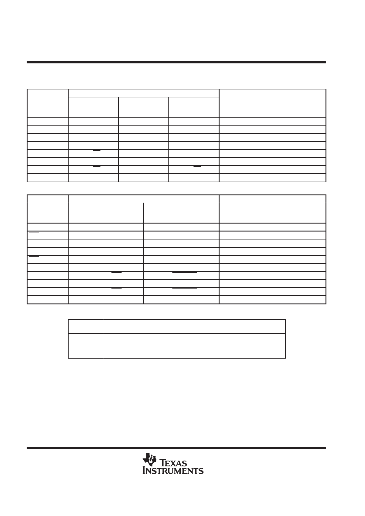
Terminal Functions
TPS2811, TPS2812, TPS2813
TERMINAL NUMBERS
TERMINAL
NAME
TPS2811
Dual Inverting
Drivers
TPS2812
Dual Noninverting
Drivers
TPS2813
Complimentary
Drivers
DESCRIPTION
REG_IN 1 1 1 Regulator input
1IN 2 2 2 Input 1
GND 3 3 3 Ground
2IN 4 4 4 Input 2
2OUT 5 = 2IN 5 = 2IN 5 = 2IN Output 2
V
CC
6 6 6 Supply voltage
1OUT 7 = 1IN 7 = 1IN 7 = 1IN Output 1
REG_OUT 8 8 8 Regulator output
TPS2814, TPS2815
TERMINAL NUMBERS
TERMINAL
NAME
TPS2814
Dual AND Drivers with Single
Inverting Input
TPS2815
Dual NAND Drivers
DESCRIPTION
1IN1 1 1 Noninverting input 1 of driver 1
1IN2 2 - Inverting input 2 of driver 1
1IN2 - 2 Noninverting input 2 of driver 1
2IN1 3 3 Noninverting input 1 of driver 2
2IN2 4 - Inverting input 2 of driver 2
2IN2 - 4 Noninverting input 2 of driver 2
2OUT 5 = 2IN1 • 2IN2 5 = 2IN1 • 2IN2 Output 2
V
CC
6 6 Supply voltage
1OUT 7 = 1IN1 • 1IN2 7 = 1IN1 • 1IN2 Output 1
GND 8 8 Ground
DISSIPATION RATING TABLE
PACKAGE
TA ≤ 25°C
POWER RATING
DERATING FACTOR
ABOVE TA = 25°C
TA = 70°C
POWER RATING
TA = 85°C
POWER RATING
P 1090 mW 8.74 mW/°C 697 mW 566 mW
D 730 mW 5.84 mW/°C 467 mW 380 mW
PW 520 mW 4.17 mW/°C 332 mW 270 mW
TPS2811, TPS2812, TPS2813, TPS2814, TPS2815
DUAL HIGH-SPEED MOSFET DRIVERS
SLVS132D – NOVEMBER 1995 – REVISED NOVEMBER 1997
5
POST OFFICE BOX 655303 • DALLAS, TEXAS 75265
absolute maximum ratings over operating free-air temperature range (unless otherwise noted)
†
Regulator input voltage range, REG_IN –0.3 V to 42 V. . . . . . . . . . . . . . . . . . . . . . . . . . . . . . . . . . . . . . . . . . . . . .
Supply voltage, V
CC
–0.3 V to 15 V. . . . . . . . . . . . . . . . . . . . . . . . . . . . . . . . . . . . . . . . . . . . . . . . . . . . . . . . . . . . . .
Input voltage range, 1IN, 2IN, 1IN1, 1IN2, 1IN2
, 2IN1, 2IN2, 2IN2 –0.3 V to V
CC
. . . . . . . . . . . . . . . . . . . . . . .
Continuous regulator output current, REG_OUT 25 mA. . . . . . . . . . . . . . . . . . . . . . . . . . . . . . . . . . . . . . . . . . . . .
Continuous output current, 1OUT, 2OUT ±100 mA. . . . . . . . . . . . . . . . . . . . . . . . . . . . . . . . . . . . . . . . . . . . . . . . . .
Continuous total power dissipation See Dissipation Rating Table. . . . . . . . . . . . . . . . . . . . . . . . . . . . . . . . . . . . .
Operating ambient temperature range, T
A
–40°C to 125°C. . . . . . . . . . . . . . . . . . . . . . . . . . . . . . . . . . . . . . . . . . .
Storage temperature range, T
stg
–65°C to 150°C. . . . . . . . . . . . . . . . . . . . . . . . . . . . . . . . . . . . . . . . . . . . . . . . . . .
Lead temperature 1,6 mm (1/16 inch) from case for 10 seconds 260°C. . . . . . . . . . . . . . . . . . . . . . . . . . . . . . .
†
Stresses beyond those listed under “absolute maximum ratings” may cause permanent damage to the device. These are stress ratings only, and
functional operation of the device at these or any other conditions beyond those indicated under “recommended operating conditions” is not
implied. Exposure to absolute-maximum-rated conditions for extended periods may affect device reliability.
NOTE 1: All voltages are with respect to device GND pin.
recommended operating conditions
MIN MAX UNIT
Regulator input voltage range 8 40 V
Supply voltage, V
CC
4 14 V
Input voltage, 1IN1, 1IN2, 1IN2, 2IN1, 2IN2, 2IN2, 1IN, 2IN –0.3 V
CC
V
Continuous regulator output current, REG_OUT 0 20 mA
Ambient temperature operating range –40 125 °C
TPS28xx electrical characteristics over recommended operating ambient temperature range,
V
CC
= 10 V, REG_IN open for TPS2811/12/13, C
L
= 1 nF (unless otherwise noted)
inputs
PARAMETER TEST CONDITIONS MIN TYP†MAX UNIT
VCC = 5 V 3.3 4 V
Positive-going input threshold voltage
VCC = 10 V 5.8 9 V
VCC = 14 V 8.3 13 V
VCC = 5 V 1 1.6 V
Negative-going input threshold voltage
VCC = 10 V 1 4.2 V
VCC = 14 V 1 6.2 V
Input hysteresis VCC = 5 V 1.6 V
Input current Inputs = 0 V or V
CC
–1 0.2 1 µA
Input capacitance 5 10 pF
†
Typicals are for TA = 25°C unless otherwise noted.
outputs
PARAMETER TEST CONDITIONS MIN TYP†MAX UNIT
p
IO = –1 mA 9.75 9.9
High-level output voltage
IO = –100 mA 8 9.1
V
p
IO = 1 mA 0.18 0.25
Low-level output voltage
IO = 100 mA 1 2
V
Peak output current VCC = 10 V 2 A
†
Typicals are for TA = 25°C unless otherwise noted.
TPS2811, TPS2812, TPS2813, TPS2814, TPS2815
DUAL HIGH-SPEED MOSFET DRIVERS
SLVS132D – NOVEMBER 1995 – REVISED NOVEMBER 1997
6
POST OFFICE BOX 655303 • DALLAS, TEXAS 75265
regulator (TPS2811/2812/2813 only)
PARAMETER TEST CONDITIONS MIN TYP†MAX UNIT
Output voltage 14 ≤ REG_IN ≤ 40 V, 0 ≤ IO ≤ 20 mA 10 11.5 13 V
Output voltage in dropout IO = 10 mA, REG_IN = 10 V 9 9.6 V
†
Typicals are for TA = 25°C unless otherwise noted.
supply current
PARAMETER TEST CONDITIONS MIN TYP†MAX UNIT
Supply current into V
CC
Inputs high or low 0.2 5 µA
Supply current into REG_IN REG_IN = 20 V, REG_OUT open 40 100 µA
†
Typicals are for TA = 25°C unless otherwise noted.
TPS28xxY electrical characteristics at TA = 25°C, V
CC
= 10 V, REG_IN open for TPS2811/12/13,
C
L
= 1 nF (unless otherwise noted)
inputs
PARAMETER TEST CONDITIONS MIN TYP MAX UNIT
VCC = 5 V 3.3 V
Positive-going input threshold voltage
VCC = 10 V 5.8 V
VCC = 14 V 8.2 V
VCC = 5 V 1.6 V
Negative-going input threshold voltage
VCC = 10 V 3.3 V
VCC = 14 V 4.2 V
Input hysteresis VCC = 5 V 1.2 V
Input current Inputs = 0 V or V
CC
0.2 µA
Input capacitance 5 pF
outputs
PARAMETER TEST CONDITIONS MIN TYP MAX UNIT
p
IO = –1 mA 9.9
High-level output voltage
IO = –100 mA 9.1
V
p
IO = 1 mA 0.18
Low-level output voltage
IO = 100 mA 1
V
Peak output current VCC = 10.5 V 2 A
regulator (TPS2811, 2812, 2813)
PARAMETER TEST CONDITIONS MIN TYP MAX UNIT
Output voltage 14 ≤ REG_IN ≤ 40 V, 0 ≤ IO ≤ 20 mA 11.5 V
Output voltage in dropout IO = 10 mA, REG_IN = 10 V 9.6 V
power supply current
PARAMETER TEST CONDITIONS MIN TYP MAX UNIT
Supply current into V
CC
Inputs high or low 0.2 µA
Supply current into REG_IN REG_IN = 20 V, REG_OUT open 40 µA
TPS2811, TPS2812, TPS2813, TPS2814, TPS2815
DUAL HIGH-SPEED MOSFET DRIVERS
SLVS132D – NOVEMBER 1995 – REVISED NOVEMBER 1997
7
POST OFFICE BOX 655303 • DALLAS, TEXAS 75265
switching characteristics for all devices over recommended operating ambient temperature range,
REG_IN open for TPS2811/12/13, C
L
= 1 nF (unless otherwise specified)
PARAMETER TEST CONDITIONS MIN TYP MAX UNIT
VCC = 14 V 14 25
t
r
Rise time
VCC = 10 V
15 30
ns
VCC = 5 V 20 35
VCC = 14 V 15 25
t
f
Fall time
VCC = 10 V
15 30
ns
VCC = 5 V 18 35
VCC = 14 V 25 40
t
PHL
Prop delay time high-to-low-level output
VCC = 10 V 25 45
ns
VCC = 5 V 34 50
VCC = 14 V 24 40
t
PLH
Prop delay time low-to-high-level output
VCC = 10 V
26 45
ns
VCC = 5 V 36 50
PARAMETER MEASUREMENT INFORMATION
Regulator
50 Ω
0.1 µF 4.7 µF
+
V
CC
1 nF
1
2
3
4
8
7
6
5
Input Output
TPS2811
NOTE A: Input rise and fall times should be ≤10 ns for accurate measurement of ac parameters.
Figure 1. Test Circuit For Measurement of Switching Characteristics
TPS2811, TPS2812, TPS2813, TPS2814, TPS2815
DUAL HIGH-SPEED MOSFET DRIVERS
SLVS132D – NOVEMBER 1995 – REVISED NOVEMBER 1997
8
POST OFFICE BOX 655303 • DALLAS, TEXAS 75265
PARAMETER MEASUREMENT INFORMATION
0–10 V dc
xOUT
0.1 µF 4.7 µF
10 V
Current
Loop
1
2
3
4
8
7
6
5
TPS2811
Regulator
+
V
CC
Figure 2. Shoot-through Current Test Setup
50%
90%
1IN
1OUT
50% 50%
90%
10%
50%
10%
t
PLH
t
r
t
f
t
PHL
0 V
0 V
Figure 3. Typical Timing Diagram (TPS2811)
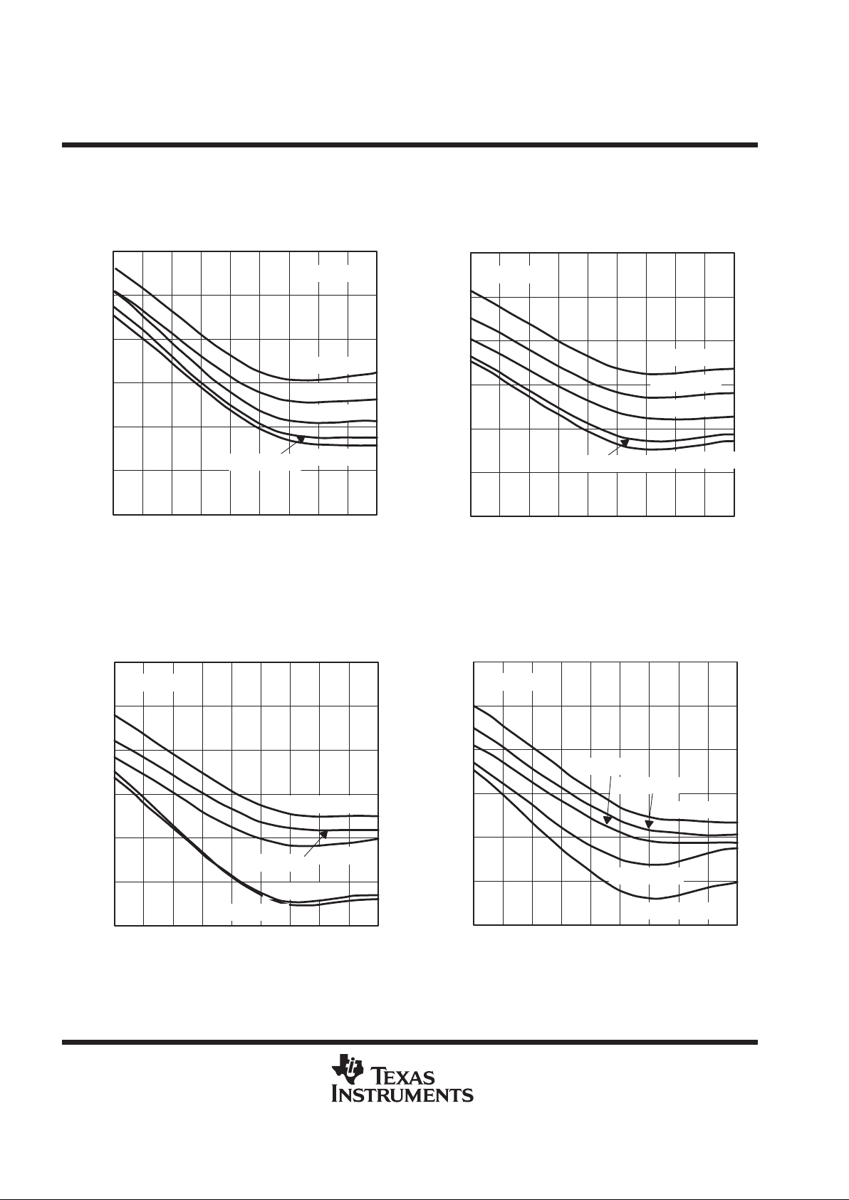
TYPICAL CHARACTERISTICS
Tables of Characteristics Graphs and Application Information
typical characteristics
PARAMETER vs PARAMETER 2 FIGURE PAGE
Rise time Supply voltage 4 10
Fall time Supply voltage 5 10
Propagation delay time Supply voltage 6, 7 10
Supply voltage 8 11
Supply current Load capacitance 9 11
Ambient temperature 10 11
Input threshold voltage Supply voltage 11 11
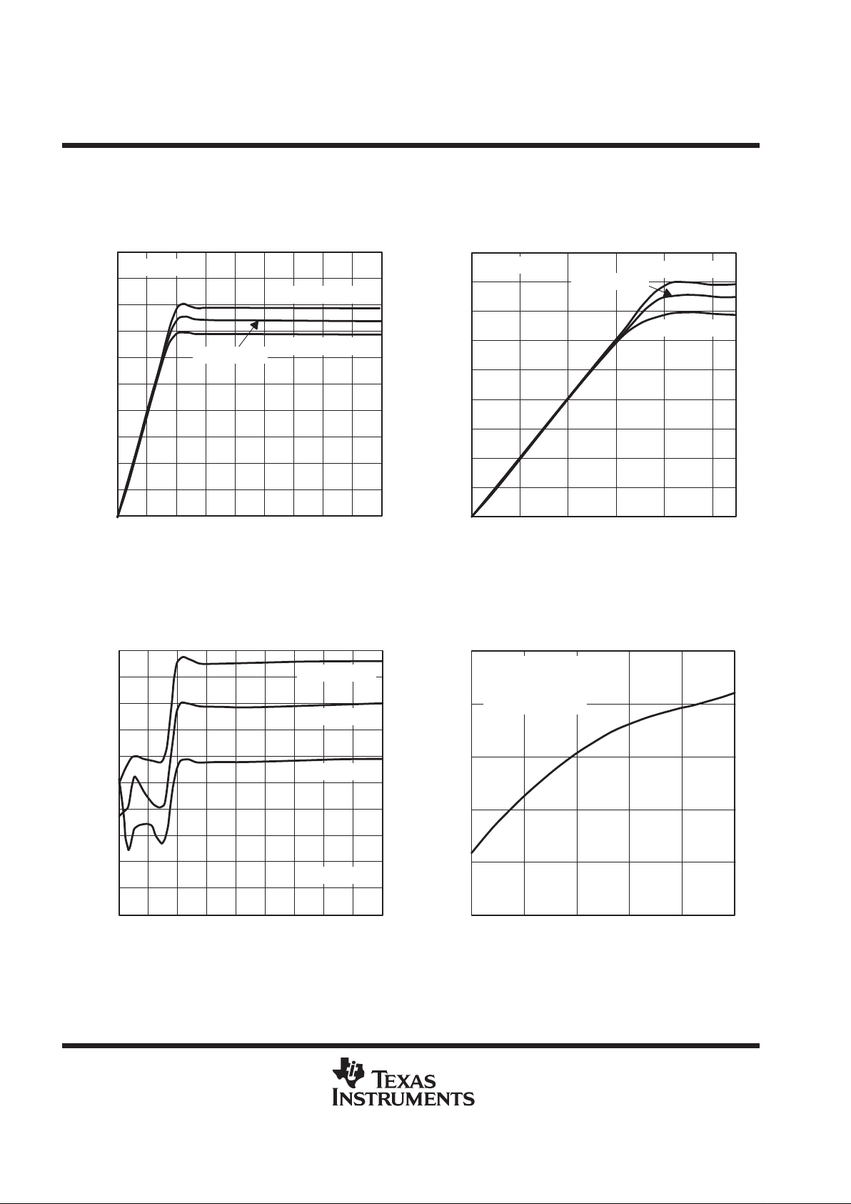
Regulator output voltage Regulator input voltage 12, 13 12
Regulator quiescent current Regulator input voltage 14 12
Peak source current Supply voltage 15 12
Peak sink current Supply voltage 16 13
Input voltage, high-to-low 17 13
Shoot-through current
Input voltage, low-to-high 18 13
TPS2811, TPS2812, TPS2813, TPS2814, TPS2815
DUAL HIGH-SPEED MOSFET DRIVERS
SLVS132D – NOVEMBER 1995 – REVISED NOVEMBER 1997
9
POST OFFICE BOX 655303 • DALLAS, TEXAS 75265
TYPICAL CHARACTERISTICS
Tables of Characteristics Graphs and Application Information (Continued)
general applications
PARAMETER vs PARAMETER 2 FIGURE PAGE
Switching test circuits and application information 19, 20 15
Low-to-high 21, 23, 25 16, 17
Voltage of 1OUT vs 2OUT
Time
High-to-low 22, 24, 26 16, 17
circuit for measuring paralleled switching characteristics
PARAMETER vs PARAMETER 2 FIGURE PAGE
Switching test circuits and application information 27 17
p
p
Low-to-high 28, 30 18
Input voltage vs output voltage
Time
High-to-low 29, 31 18
Hex-1 to Hex-4 application information
PARAMETER vs PARAMETER 2 FIGURE PAGE
Driving test circuit and application information 32 19
Hex-1 size 33 20
Hex-2 size 36 20
Drain-source voltage vs drain current Time
Hex-3 size 39 21
Hex-4 size 41 22
Hex-4 size parallel drive 45 23
Hex-1 size 34 20
Hex-2 size 37 21
Drain-source voltage vs gate-source voltage at turn-on Time
Hex-3 size 40 21
Hex-4 size 43 22
Hex-4 size parallel drive 46 23
Hex-1 size 35 20
Hex-2 size 38 21
Drain-source voltage vs gate-source voltage at turn-off Time
Hex-3 size 42 22
Hex-4 size 44 22
Hex-4 size parallel drive 47 23
synchronous buck regulator application
PARAMETER vs PARAMETER 2 FIGURE PAGE
3.3-V 3-A Synchronous-Rectified Buck Regulator Circuit 48 24
Q1 drain voltage vs gate voltage at turn-on 49 26
Q1 drain voltage vs gate voltage at turn-off 50 26
Q1 drain voltage vs Q2 gate-source voltage
Time
51, 52, 53 26, 27
p
pp
3 A 54 27
Output ripple voltage vs inductor current
5 A 55 27
TPS2811, TPS2812, TPS2813, TPS2814, TPS2815
DUAL HIGH-SPEED MOSFET DRIVERS
SLVS132D – NOVEMBER 1995 – REVISED NOVEMBER 1997
10
POST OFFICE BOX 655303 • DALLAS, TEXAS 75265
TYPICAL CHARACTERISTICS
Figure 4
16
14
12
10
5678910
– Rise Time – ns
18
20
RISE TIME
vs
SUPPLY VOLTAGE
22
11 12 13 14
CL = 1 nF
TA = 125°C
TA = 75°C
TA = 25°C
TA = –25°C
TA = –50°C
t
r
VCC – Supply Voltage – V
Figure 5
16
14
12
10
5678910
– Fall Time – ns
18
20
FALL TIME
vs
SUPPLY VOLTAGE
22
11 12 13 14
CL = 1 nF
TA = 125°C
TA = 75°C
TA = 25°C
TA = –25°C
TA = –50°C
t
f
VCC – Supply Voltage – V
Figure 6
30
25
20
15
56 78910
35
40
45
11 12 13 14
CL = 1 nF
TA = 125°C
TA = 75°C
TA = 25°C
TA = –25°C
TA = –50°C
Propagation Delay Time,
PROPAGATION DELAY TIME,
HIGH-TO-LOW-LEVEL OUTPUT
vs
SUPPLY VOLTAGE
VCC – Supply Voltage – V
t –
PHL
High-To-Low-Level Output – ns
Figure 7
30
25
20
15
5678 910
35
40
45
11 12 13 14
Propagation Delay Time,
PROPAGATION DELAY TIME,
LOW-TO-HIGH-LEVEL OUTPUT
vs
SUPPLY VOLTAGE
VCC – Supply Voltage – V
t –
PLH
Low-To-High-Level Output – ns
CL = 1 nF
TA = –50°C
TA = 75°C
TA = –25°C
TA=125°C
TA = 25°C

TPS2811, TPS2812, TPS2813, TPS2814, TPS2815
DUAL HIGH-SPEED MOSFET DRIVERS
SLVS132D – NOVEMBER 1995 – REVISED NOVEMBER 1997
11
POST OFFICE BOX 655303 • DALLAS, TEXAS 75265
TYPICAL CHARACTERISTICS
Figure 8
8
6
2
0
46810
Supply Current – mA
10
14
SUPPLY CURRENT
vs
SUPPLY VOLTAGE
16
12 14
4
12
Duty Cycle = 50%
CL = 1 nF
1 MHz
40 kHz
500 kHz
100 kHz
75 kHz
VCC – Supply Voltage – V
I –
CC
Figure 9
1.5
1
0.5
0
0 0.5 1
Supply Current – mA
2
SUPPLY CURRENT
vs
LOAD CAPACITANCE
2.5
1.5 2
VCC = 10 V
f = 100 kHz
TA = 25°C
CL – Load Capacitance – nF
I –
CC
Figure 10
1.15
1.13
1.12
1.1
–50 –25 0 25 50
1.16
1.18
1.2
75 100 125
1.19
1.17
1.14
1.11
Supply Current – mA
SUPPLY CURRENT
vs
AMBIENT TEMPERATURE
CL = 1 nF
VCC = 10 V
Duty Cycle = 50%
f = 100 kHz
TA – Temperature – ° C
I –
CC
Figure 11
TA = 25°C
5
3
2
0
46810
Input Threshold Voltage – V
7
8
9
12 14
6
4
1
+ Threshold
– Threshold
INPUT THRESHOLD VOLTAGE
vs
SUPPLY VOLTAGE
VCC – Supply Voltage – V
V –
IT
TPS2811, TPS2812, TPS2813, TPS2814, TPS2815
DUAL HIGH-SPEED MOSFET DRIVERS
SLVS132D – NOVEMBER 1995 – REVISED NOVEMBER 1997
12
POST OFFICE BOX 655303 • DALLAS, TEXAS 75265
TYPICAL CHARACTERISTICS
Figure 12
9
8
7
4 8 12 16 20 24
11
12
14
28 32 36 40
Regulator Output Voltage – V
REGULATOR OUTPUT VOLTAGE
vs
REGULATOR INPUT VOLTAGE
TA = –55°C
TA = 25°C
TA = 125°C
RL = 10 kΩ
Regulator Input Voltage – V
13
10
6
5
4
Figure 13
8
6
5
46 810
10
12
13
12 14
11
9
7
4
Regulator Output Voltage – V
REGULATOR OUTPUT VOLTAGE
vs
REGULATOR INPUT VOLTAGE
TA = 125°C
TA = –55°C
TA = 25°C
RL = 10 kΩ
Regulator Input Voltage – V
Figure 14
25
20
10
0
4 8 12 16 20 24
35
45
50
28 32 36 40
TA = 25°C
TA = 125°C
TA = –55°C
40
30
15
5
Regulator Quiescent Current –
REGULATOR QUIESCENT CURRENT
vs
REGULATOR INPUT VOLTAGE
Aµ
RL = 10 kΩ
Regulator Input Voltage – V
Figure 15
1
.5
0
46810
1.5
2
2.5
12 14
Peak Source Current – A
PEAK SOURCE CURRENT
vs
SUPPLY VOLTAGE
VCC – Supply Voltage – V
RL = 0.5 Ω
f = 100 kHz
Duty Cycle = 5%
TA = 25°C

TPS2811, TPS2812, TPS2813, TPS2814, TPS2815
DUAL HIGH-SPEED MOSFET DRIVERS
SLVS132D – NOVEMBER 1995 – REVISED NOVEMBER 1997
13
POST OFFICE BOX 655303 • DALLAS, TEXAS 75265
TYPICAL CHARACTERISTICS
1
.5
0
46810
1.5
2
2.5
12 14
Peak Sink Current – A
PEAK SINK CURRENT
vs
SUPPLY VOLTAGE
VCC – Supply Voltage – V
RL = 0.5 Ω
f = 100 kHz
Duty Cycle = 5%
TA = 25°C
Figure 16
Figure 17
3
2
1
0
10 8 6 4
4
5
6
20
Shoot-Through Current – mA
SHOOT-THROUGH CURRENT
vs
INPUT VOLTAGE, HIGH-TO-LOW
VI – Input Voltage, High-to-Low – V
VCC = 10 V
CL = 0
TA = 25°C
Figure 18
3
2
1
0246
4
5
6
810
SHOOT-THROUGH CURRENT
vs
INPUT VOLTAGE, LOW-TO-HIGH
VI – Input Voltage, Low-to-High – V
VCC = 10 V
CL = 0
TA = 25°C
Shoot-Through Current – mA
0

TPS2811, TPS2812, TPS2813, TPS2814, TPS2815
DUAL HIGH-SPEED MOSFET DRIVERS
SLVS132D – NOVEMBER 1995 – REVISED NOVEMBER 1997
14
POST OFFICE BOX 655303 • DALLAS, TEXAS 75265
APPLICATION INFORMATION
The TPS2811, TPS2812 and TPS2813 circuits each contain one regulator and two MOSFET drivers. The
regulator can be used to limit V
CC
to between 10 V and 13 V for a range of input voltages from 14 V to 40 V,
while providing up to 20 mA of dc drive. The TPS2814 and TPS2815 both contain two drivers, each of which
has two inputs. The TPS281 1 has inverting drivers, the TPS2812 has noninverting drivers, and the TPS2813
has one inverting and one noninverting driver. The TPS2814 is a dual 2-input AND driver with one inverting input
on each driver, and the TPS2815 is a dual 2-input NAND driver . These MOSFET drivers are capable of supplying
up to 2.1 A or sinking up to 1.9 A (see Figures 15 and 16) of instantaneous current to n-channel or p-channel
MOSFETs. The TPS2811 family of MOSFET drivers have very fast switching times combined with very short
propagation delays. These features enhance the operation of today’s high-frequency circuits.
The CMOS input circuit has a positive threshold of approximately 2/3 of V
CC
, with a negative threshold of 1/3 of
V
CC
, and a very high input impedance in the range of 10
9
Ω. Noise immunity is also very high because of the
Schmidt trigger switching. In addition, the design is such that the normal shoot-through current in CMOS (when
the input is biased halfway between V
CC
and ground) is limited to less than 6 mA. The limited shoot-through
is evident in the graphs in Figures 17 and 18. The input stage shown in the functional block diagram better
illustrates the way the front end works. The circuitry of the device is such that regardless of the rise and/or fall
time of the input signal, the output signal will always have a fast transition speed; this basically isolates the
waveforms at the input from the output. Therefore, the specified switching times are not affected by the slopes
of the input waveforms.
The basic driver portion of the circuits operate over a supply voltage range of 4 V to 14 V with a maximum bias
current of 5 µA. Each driver consists of a CMOS input and a buffered output with a 2-A instantaneous drive
capability. They have propagation delays of less than 30 ns and rise and fall times of less than 20 ns each.
Placing a 0.1-µF ceramic capacitor between V
CC
and ground is recommended; this will supply the
instantaneous current needed by the fast switching and high current surges of the driver when it is driving a
MOSFET.
The output circuit is also shown in the functional block diagram. This driver uses a unique combination of a
bipolar transistor in parallel with a MOSFET for the ability to swing from V
CC
to ground while providing 2 A of
instantaneous driver current. This unique parallel combination of bipolar and MOSFET output transistors
provides the drive required at V
CC
and ground to guarantee turn-off of even low-threshold MOSFETs. Typical
bipolar-only output devices don’t easily approach V
CC
or ground.
The regulator, included in the TPS2811, TPS2812 and TPS2813, has an input voltage range of 14 V to 40 V.
It produces an output voltage of 10 V to 13 V and is capable of supplying from 0 to 20 mA of output current. In
grounded source applications, this extends the overall circuit operation to 40 V by clamping the driver supply
voltage (V
CC
) to a safe level for both the driver and the MOSFET gate. The bias current for full operation is a
maximum of 150 µA. A 0.1-µF capacitor connected between the regulator output and ground is required to
ensure stability . For transient response, an additional 4.7-µ F electrolytic capacitor on the output and a 0.1-µF
ceramic capacitor on the input will optimize the performance of this circuit. When the regulator is not in use, it
can be left open at both the input and the output, or the input can be shorted to the output and tied to either the
V
CC
or the ground pin of the chip.

TPS2811, TPS2812, TPS2813, TPS2814, TPS2815
DUAL HIGH-SPEED MOSFET DRIVERS
SLVS132D – NOVEMBER 1995 – REVISED NOVEMBER 1997
15
POST OFFICE BOX 655303 • DALLAS, TEXAS 75265
APPLICATION INFORMATION
matching and paralleling connections
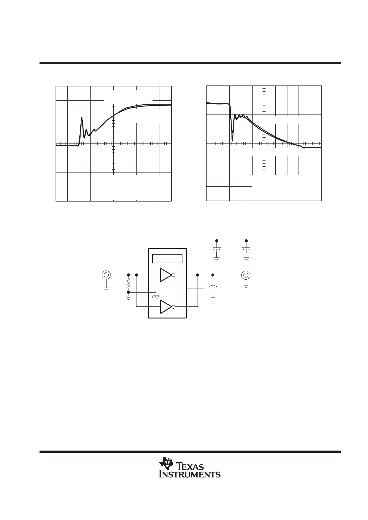
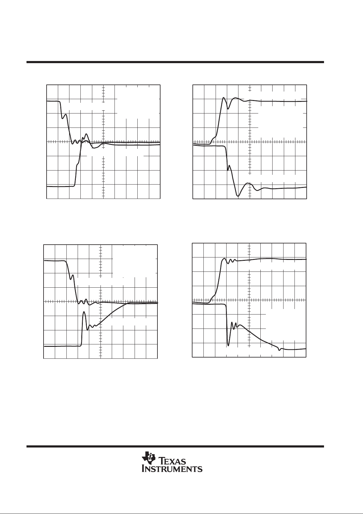
Figures 21 and 22 show the delays for the rise and fall time of each channel. As can be seen on a 5-ns scale,
there is very little difference between the two channels at no load. Figures 23 and 24 show the difference
between the two channels for a 1-nF load on each output. There is a slight delay on the rising edge, but little
or no delay on the falling edge. As an example of extreme overload, Figures 25 and 26 show the difference
between the two channels, or two drivers in the package, each driving a 10-nF load. As would be expected, the
rise and fall times are significantly slowed down. Figures 28 and 29 show the effect of paralleling the two
channels and driving a 1-nF load. A noticeable improvement is evident in the rise and fall times of the output
waveforms. Finally , Figures 30 and 31 show the two drivers being paralleled to drive the 10-nF load and as could
be expected the waveforms are improved. In summary , the paralleling of the two drivers in a package enhances
the capability of the drivers to handle a larger load. Because of manufacturing tolerances, it is not recommended
to parallel drivers that are not in the same package.
Regulator
50 Ω
1
2
3
4
8
7
6
5
1 nF
Output
0.1 µF 4.7 µF
+
V
CC
TPS2811
Figure 19. Test Circuit for Measuring Switching Characteristics
Regulator
50 Ω
1
2
3
4
8
7
6
5
C
L(2)
C
L(1)
Output 1
0.1 µF 4.7 µF
+
V
CC
TPS2811
NOTE A: Input rise and fall times should be ≤10 ns for accurate measurement of ac parameters.
Output 2
Figure 20. Test Circuit for Measuring Switching Characteristics with the Inputs Connected in Parallel

TPS2811, TPS2812, TPS2813, TPS2814, TPS2815
DUAL HIGH-SPEED MOSFET DRIVERS
SLVS132D – NOVEMBER 1995 – REVISED NOVEMBER 1997
16
POST OFFICE BOX 655303 • DALLAS, TEXAS 75265
APPLICATION INFORMATION
Figure 21. Voltage of 1OUT vs Voltage at
2OUT, Low-to-High Output Delay
t – Time
TA = 25°C
VI = 14 V
CL = 0
Paralleled Inputs
VO at 2OUT (5 V/div, 5 ns/div)
VO at 1OUT (5 V/div, 5 ns/div)
t – Time
TA = 25°C
VI = 14 V
CL = 0
Paralleled Input
VO at 2OUT (5 V/div, 5 ns/div)
VO at 1OUT (5 V/div, 5 ns/div)
Figure 22. Voltage at 1OUT vs Voltage
at 2OUT, High-to-Low Output Delay
t – Time
TA = 25°C
VI = 14 V
CL = 1 nF Each Output
Paralleled Input
VO at 2OUT
(5 V/div, 10 ns/div)
VO at 1OUT (5 V/div, 10 ns/div)
Figure 23. Voltage at 1OUT vs Voltage at
2OUT, Low-to-High Output Delay
t – Time
VO at 2OUT (5 V/div, 10 ns/div)
VO at 1OUT
(5 V/div, 10 ns/div)
TA = 25°C
VI = 14 V
CL = 1 nF on Each Output
Paralleled Input
Figure 24. Voltage at 1OUT vs Voltage at
2OUT, High-to-Low Output Delay
TPS2811, TPS2812, TPS2813, TPS2814, TPS2815
DUAL HIGH-SPEED MOSFET DRIVERS
SLVS132D – NOVEMBER 1995 – REVISED NOVEMBER 1997
17
POST OFFICE BOX 655303 • DALLAS, TEXAS 75265
APPLICATION INFORMATION
t – Time
TA = 25°C
VCC = 14 V
CL = 10 nF on Each Output
Paralleled Input
VO at 2OUT
(5 V/div, 20 ns/div)
VO at 1OUT
(5 V/div, 20 ns/div)
Figure 25. Voltage at 1OUT vs Voltage at
2OUT, Low-to-High Output Delay
t – Time
TA = 25°C
VCC = 14 V
CL = 10 nF on Each Output
Paralleled Input
VO at 2OUT (5 V/div, 20 ns/div)
VO at (5 V/div, 20 ns/div)
Figure 26. Voltage at 1OUT vs Voltage at
2OUT, High-to-Low Output Delay
Regulator
50 Ω
1
2
3
4
8
7
6
5
C
L
Output
0.1 µF 4.7 µF
+
V
CC
TPS2811
NOTE A: Input rise and fall times should be ≤10 ns for accurate measurement of ac parameters.
Figure 27. Test Circuit for Measuring Paralleled Switching Characteristics
TPS2811, TPS2812, TPS2813, TPS2814, TPS2815
DUAL HIGH-SPEED MOSFET DRIVERS
SLVS132D – NOVEMBER 1995 – REVISED NOVEMBER 1997
18
POST OFFICE BOX 655303 • DALLAS, TEXAS 75265
APPLICATION INFORMATION
t – Time
TA = 25°C
VCC = 14 V
CL = 1 nF
Paralleled Input
and Output
VO (5 V/div, 20 ns/div)
VI (5 V/div, 20 ns/div)
Figure 28. Input Voltage vs Output Voltage,
Low-to-High Propagation Delay of Paralleled
Drivers
t – Time
TA = 25°C
VCC = 14 V
CL = 1 nF
Paralleled Input
and Output
VO (5 V/div, 20 ns/div)
VI (5 V/div, 20 ns/div)
Figure 29. Input Voltage vs Output Voltage,
High-to-Low Propagation Delay of Paralleled
Drivers
t – Time
TA = 25°C
VCC = 14 V
CL = 10 nF
Paralleled Input
and Output
VO (5 V/div, 20 ns/div)
VI (5 V/div, 20 ns/div)
Figure 30. Input Voltage vs Output Voltage,
Low-to-High Propagation Delay of Paralleled
Drivers
t – Time
TA = 25°C
VCC = 14 V
CL = 10 nF
Paralleled Input
and Output
VO (5 V/div, 20 ns/div)
VI (5 V/div, 20 ns/div)
Figure 31. Input Voltage vs Output Voltage,
High-to-Low Propagation Delay of Paralleled
Drivers

TPS2811, TPS2812, TPS2813, TPS2814, TPS2815
DUAL HIGH-SPEED MOSFET DRIVERS
SLVS132D – NOVEMBER 1995 – REVISED NOVEMBER 1997
19
POST OFFICE BOX 655303 • DALLAS, TEXAS 75265
APPLICATION INFORMATION
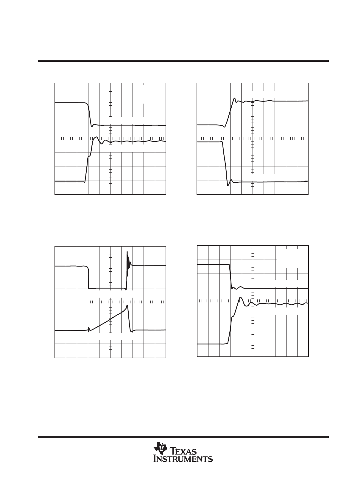
Figures 33 through 47 illustrate the performance of the TPS2811 driving MOSFETs with clamped inductive
loads, similar to what is encountered in discontinuous-mode flyback converters. The MOSFET s that were tested
range in size from Hex-1 to Hex-4, although the TPS28xx family is only recommended for Hex-3 or below.
The test circuit is shown in Figure 32. The layout rules observed in building the test circuit also apply to real
applications. Decoupling capacitor C1 is a 0.1-µF ceramic device, connected between V
CC
and GND of the
TPS2811, with short lead lengths. The connection between the driver output and the MOSFET gate, and
between GND and the MOSFET source, are as short as possible to minimize inductance. Ideally , GND of the
driver is connected directly to the MOSFET source. The tests were conducted with the pulse generator
frequency set very low to eliminate the need for heat sinking, and the duty cycle was set to turn off the MOSFET
when the drain current reached 50% of its rated value. The input voltage was adjusted to clamp the drain voltage
at 80% of its rating.
As shown, the driver is capable of driving each of the Hex-1 through Hex-3 MOSFET s to switch in 20 ns or less.
Even the Hex-4 is turned on in less than 20 ns. Figures 45, 46 and 47 show that paralleling the two drivers in
a package enhances the gate waveforms and improves the switching speed of the MOSFET. Generally, one
driver is capable of driving up to a Hex-4 size. The TPS281 1 family is even capable of driving large MOSFETs
that have a low gate charge.
Regulator
R1
50 Ω
1
2
3
4
8
7
6
5
C1
0.1 µF
C2
4.7 µF
+
–
V
DS
Q1
Current
Loop
L1
CR1
+
V
I
V
DS
V
GS
V
CC
Figure 32. TPS2811 Driving Hex-1 through Hex-4 Devices

TPS2811, TPS2812, TPS2813, TPS2814, TPS2815
DUAL HIGH-SPEED MOSFET DRIVERS
SLVS132D – NOVEMBER 1995 – REVISED NOVEMBER 1997
20
POST OFFICE BOX 655303 • DALLAS, TEXAS 75265
APPLICATION INFORMATION
t – Time
TA = 25°C
VCC = 14 V
VI = 48 V
VDS (20 V/div, 0.5 µs/div)
ID (0.5 A/div, 0.5 µs/div)
Figure 33. Drain-Source Voltage vs Drain
Current, TPS2811 Driving an IRFD014
(Hex-1 Size)
t – Time
TA = 25°C
VCC = 14 V
VI = 48 V
VDS (20 V/div, 50 ns/div)
VGS (5 V/div, 50 ns/div)
Figure 34. Drain-Source Voltage vs
Gate-Source Voltage, at Turn-on,
TPS2811 Driving an IRFD014 (Hex-1 Size)
t – Time
TA = 25°C
VCC = 14 V
VI = 48 V
VDS (20 V/div, 50 ns/div)
VGS (5 V/div, 50 ns/div)
Figure 35. Drain-Source Voltage vs
Gate-Source Voltage, at Turn-off,
TPS2811 Driving an IRFD014 (Hex-1 Size)
t – Time
TA = 25°C
VCC = 14 V
VI = 80 V
VDS (50 V/div, 0.2 µs/div)
VGS (0.5 A/div, 0.2 µs/div)
Figure 36. Drain-Source Voltage vs Drain
Current, TPS2811 Driving an IRFD120
(Hex-2 Size)
TPS2811, TPS2812, TPS2813, TPS2814, TPS2815
DUAL HIGH-SPEED MOSFET DRIVERS
SLVS132D – NOVEMBER 1995 – REVISED NOVEMBER 1997
21
POST OFFICE BOX 655303 • DALLAS, TEXAS 75265
APPLICATION INFORMATION
t – Time
TA = 25°C
VCC = 14 V
VI = 80 V
VDS (50 V/div, 50 ns/div)
VGS (5 V/div, 50 ns/div)
Figure 37. Drain-Source Voltage vs
Gate-Source V oltage,
at Turn-on, TPS2811 Driving an IRFD120
(Hex-2 Size)
t – Time
TA = 25°C
VCC = 14 V
VI = 80 V
VDS (50 V/div, 50 ns/div)
VGS (5 V/div, 50 ns/div)
Figure 38. Drain-Source Voltage vs
Gate-Source V oltage,
at Turn-off, TPS2811 Driving an IRFD120
(Hex-2 Size)
t – Time
TA = 25°C
VCC = 14 V
VI = 80 V
VDS (50 V/div, 2 µs/div)
ID (5 A/div, 2 µs/div)
Figure 39. Drain-Source Voltage vs Drain
Current, TPS2811 Driving an IRF530
(Hex-3 Size)
t – Time
TA = 25°C
VCC = 14 V
VI = 80 V
VDS (50 V/div, 50 ns/div)
VGS (5 A/div, 50 ns/div)
Figure 40. Drain-Source Voltage vs
Gate-Source Voltage, at Turn-on, TPS2811
Driving an IRF530 (Hex-3 Size)

TPS2811, TPS2812, TPS2813, TPS2814, TPS2815
DUAL HIGH-SPEED MOSFET DRIVERS
SLVS132D – NOVEMBER 1995 – REVISED NOVEMBER 1997
22
POST OFFICE BOX 655303 • DALLAS, TEXAS 75265
APPLICATION INFORMATION
t – Time
TA = 25°C
VCC = 14 V
VI = 350 V
VDS (50 V/div, 0.2 µs/div)
ID (2 A/div,
0.2 µs/div)
Figure 41. Drain-Source Voltage vs Drain
Current,
One Driver, TPS2811 Driving an IRF840
(Hex-4 Size)
t – Time
TA = 25°C
VCC = 14 V
VI = 80 V
VDS (50 V/div, 50 ns/div)
VGS (5 V/div, 50 ns/div)
Figure 42. Drain-Source Voltage vs
Gate-Source V oltage,
at Turn-off, TPS2811 Driving an IRF530
(Hex-3 Size)
t – Time
TA = 25°C
VCC = 14 V
VI = 350 V
VDS (50 V/div, 50 ns/div)
VGS (5 V/div, 50 ns/div)
Figure 43. Drain-Source Voltage vs
Gate-Source Voltage, at Turn-on,
One Driver, TPS2811 Driving an IRF840
(Hex-4 Size)
t – Time
TA = 25°C
VCC = 14 V
VI = 350 V
VDS (50 V/div, 50 ns/div)
VGS (5 V/div, 50 ns/div)
Figure 44. Drain-Source Voltage vs Gate-Source
Voltage, at Turn-off, One Driver,
TPS2811 Driving an IRF840
(Hex-4 Size)

TPS2811, TPS2812, TPS2813, TPS2814, TPS2815
DUAL HIGH-SPEED MOSFET DRIVERS
SLVS132D – NOVEMBER 1995 – REVISED NOVEMBER 1997
23
POST OFFICE BOX 655303 • DALLAS, TEXAS 75265
APPLICATION INFORMATION
t – Time
TA = 25°C
VCC = 14 V
VI = 350 V
VDS (50 V/div, 0.2 µs/div)
ID (2 A/div,
0.2 µs/div)
Figure 45. Drain-Source Voltage vs Drain
Current, Parallel Drivers,
TPS2811 Driving an IRF840 (Hex-4 Size)
t – Time
TA = 25°C
VCC = 14 V
VI = 350 V
VDS (50 V/div,
50 ns/div)
VGS (5 V/div,
50 ns/div)
Figure 46. Drain-Source Voltage vs Gate-Source
Voltage, at Turn-on, Parallel Drivers,
TPS2811 Driving an IRF840 (Hex-4 Size)
t – Time
TA = 25°C
VCC = 14 V
VI = 350 V
VGS (5 V/div, 50 ns/div)
VDS (50 V/div, 50 ns/div)
Figure 47. Drain-Source Voltage vs Gate-Source Voltage, at Turn-off,
Parallel Drivers, TPS2811 Driving an IRF840 (Hex-4 Size)

TPS2811, TPS2812, TPS2813, TPS2814, TPS2815
DUAL HIGH-SPEED MOSFET DRIVERS
SLVS132D – NOVEMBER 1995 – REVISED NOVEMBER 1997
24
POST OFFICE BOX 655303 • DALLAS, TEXAS 75265
APPLICATION INFORMATION
synchronous buck regulator
Figure 48 is the schematic for a 100-kHz synchronous-rectified buck converter implemented with a TL5001
pulse-width-modulation (PWM) controller and a TPS2812 driver. The bill of materials is provided in Table 1. The
converter operates over an input range from 5.5 V to 12 V and has a 3.3-V output capable of supplying 3 A
continuously and 5 A during load surges. The converter achieves an efficiency of 90.6% at 3 A and 87.6% at
5 A. Figures 49 and 50 show the power switch switching performance. The output ripple voltage waveforms are
documented in Figures 54 and 55.
The TPS2812 drives both the power switch, Q2, and the synchronous rectifier, Q1. Large shoot-through
currents, caused by power switch and synchronous rectifier remaining on simultaneously during the transitions,
are prevented by small delays built into the drive signals, using CR2, CR3, R1 1, R12, and the input capacitance
of the TPS2812. These delays allow the power switch to turn off before the synchronous rectifier turns on and
vice versa. Figure 51 shows the delay between the drain of Q2 and the gate of Q1; expanded views are provided
in Figures 52 and 53.
REG_IN
1 IN
GND
2 IN
REG_OUT
1 OUT
V
CC
2 OUT
U2
TPS2812D
1
2
3
4
8
7
6
5
Q1
IRF7406
13
2
R5
10 kΩ
C11
0.47 µF
C100
100 µF
16 V
C5
100 µF
16 V
1
2
3
4
J1
2
1
Q2
IRF7201
3
CR1
30BQ015
C6
1000 pF
R7
3.3 Ω
L1
27 µF
C12
100 µF
16 V
C7
100 µF
16 V
C13
10 µF
10 V
1
2
3
4
J2
V
I
VI
GND
GND
3.3 V
3.3 V
GND
GND
U1
TL5001CD
OUT V
CC
COMP FB
GND RT DTC SCP
R2
1.6 kΩ
C3
0.0022
µF
C2
0.033 µF
R13
10 kΩ
C14
0.1 µF
R6
15 Ω
R10
1 kΩ
R11
30 kΩ
CR2
BAS16ZX
R12
10 kΩ
CR3
BAS16ZX
C15
1 µF
R8
121 kΩ
1%
C9
0.22 µF
C1
1 µF
R4
2.32 kΩ
1%
R3
180 Ω
C4
0.022 µF
R1
1.00 kΩ
1%
R9
90.9 kΩ
1%
8765
1234
+
+
++
+
Figure 48. 3.3-V 3-A Synchronous-Rectified Buck Regulator Circuit

TPS2811, TPS2812, TPS2813, TPS2814, TPS2815
DUAL HIGH-SPEED MOSFET DRIVERS
SLVS132D – NOVEMBER 1995 – REVISED NOVEMBER 1997
25
POST OFFICE BOX 655303 • DALLAS, TEXAS 75265
APPLICATION INFORMATION
Table 1. Bill of Materials,
3.3-V, 3-A Synchronous-Rectified Buck Converter
REFERENCE DESCRIPTION VENDOR
U1 TL5001CD, PWM Texas Instruments, 972-644-5580
U2 TPS2812D, N.I. MOSFET Driver Texas Instruments, 972-644-5580
CR1 3 A, 15 V, Schottky , 30BQ015 International Rectifier, 310-322-3331
CR2,CR3 Signal Diode, BAS16ZX Zetex, 516-543-7100
C1 1 µF, 16 V, Tantalum
C2 0.033 µF, 50 V
C3 0.0022 µF, 50 V
C4 0.022 µF, 50 V
C5,C7,C10,C12 100 µF, 16 V, Tantalum, TPSE107M016R0100 AVX, 800-448-9411
C6 1000 pF, 50 V
C9 0.22 µF, 50 V
C11 0.47 µF, 50 V, Z5U
C13 10 µF, 10 V, Ceramic, CC1210CY5V106Z TDK, 708-803-6100
C14 0.1 µF, 50 V
C15 1.0 µF, 50 V
J1,J2 4-Pin Header
L1 27 µH, 3 A/5 A, SML5040 Nova Magnetics, Inc., 972-272-8287
Q1 IRF7406, P-FET International Rectifier, 310-322-3331
Q2 IRF7201, N-FET International Rectifier , 310-322-3331
R1 1.00 kΩ, 1%
R2 1.6 kΩ
R3 180 Ω
R4 2.32 kΩ, 1 %
R5,R12,R13 10 kΩ
R6 15 Ω
R7 3.3 Ω
R8 121 kΩ, 1%
R9 90.9 kΩ, 1%
R10 1 kΩ
R11 30 kΩ
NOTES: 2. Unless otherwise specified, capacitors are X7R ceramics.
3. Unless otherwise specified, resistors are 5%, 1/10 W.

TPS2811, TPS2812, TPS2813, TPS2814, TPS2815
DUAL HIGH-SPEED MOSFET DRIVERS
SLVS132D – NOVEMBER 1995 – REVISED NOVEMBER 1997
26
POST OFFICE BOX 655303 • DALLAS, TEXAS 75265
APPLICATION INFORMATION
t – Time
VD (5 V/div, 20 ns/div)
VG (2 V/div, 20 ns/div)
TA = 25°C
VI = 12 V
VO = 3.3 V at 5A
Figure 49. Q1 Drain Voltage vs Gate Voltage,
at Switch Turn-on
Figure 50. Q1 Drain Voltage vs Gate Voltage,
at Switch Turn-off
t – Time
VD (5 V/div, 20 ns/div)
VG (2 V/div, 20 ns/div)
TA = 25°C
VI = 12 V
VO = 3.3 V at 5A
t – Time
VGS (2 V/div, 0.5 µs/div)
TA = 25°C
VI = 12 V
VO = 3.3 V at 5A
VD (5 V/div, 0.5 µs/div)
Figure 51. Q1 Drain Voltage vs Q2
Gate-Source V oltage
t – Time
VGS (2 V/div, 20 ns/div)
TA = 25°C
VI = 12 V
VO = 3.3 V at 5A
VD (5 V/div, 20 ns/div)
Figure 52. Q1 Drain Voltage vs Q2
Gate-Source V oltage

TPS2811, TPS2812, TPS2813, TPS2814, TPS2815
DUAL HIGH-SPEED MOSFET DRIVERS
SLVS132D – NOVEMBER 1995 – REVISED NOVEMBER 1997
27
POST OFFICE BOX 655303 • DALLAS, TEXAS 75265
APPLICATION INFORMATION
t – Time
VGS (2 V/div, 20 ns/div)
TA = 25°C
VI = 12 V
VO = 3.3 V at 5A
VD (5 V/div, 20 ns/div)
Figure 53. Q1 Drain Voltage vs Q2 Gate-Source Voltage
t – Time
Output Ripple Voltage (20 mV/div, 2 µs/div)
Inductor Current (1 A/div, 2 µs/div)
TA = 25°C
VI = 12 V
VO = 3.3 V at 3A
1
2
Figure 54. Output Ripple Voltage vs
Inductor Current, at 3 A
t – Time
Output Ripple Voltage (20 mV/div, 2 µs/div)
Inductor Current (2 A/div, 2 µs/div)
TA = 25°C
VI = 12 V
VO = 3.3 V at 5 A
1
2
Figure 55. Output Ripple Voltage vs
Inductor Current, at 5 A
TPS2811, TPS2812, TPS2813, TPS2814, TPS2815
DUAL HIGH-SPEED MOSFET DRIVERS
SLVS132D – NOVEMBER 1995 – REVISED NOVEMBER 1997
28
POST OFFICE BOX 655303 • DALLAS, TEXAS 75265
MECHANICAL DATA
D (R-PDSO-G**) PLASTIC SMALL-OUTLINE PACKAGE
14 PIN SHOWN
4040047/B 03/95
0.228 (5,80)
0.244 (6,20)
0.069 (1,75) MAX
0.010 (0,25)
0.004 (0,10)
1
14
0.014 (0,35)
0.020 (0,51)
A
0.157 (4,00)
0.150 (3,81)
7
8
0.044 (1,12)
0.016 (0,40)
Seating Plane
0.010 (0,25)
PINS **
0.008 (0,20) NOM
A MIN
A MAX
DIM
Gage Plane
0.189
(4,80)
(5,00)
0.197
8
(8,55)
(8,75)
0.337
14
0.344
(9,80)
16
0.394
(10,00)
0.386
0.004 (0,10)
M
0.010 (0,25)
0.050 (1,27)
0°–8°
NOTES: A. All linear dimensions are in inches (millimeters).
B. This drawing is subject to change without notice.
C. Body dimensions do not include mold flash or protrusion, not to exceed 0.006 (0,15).
D. Four center pins are connected to die mount pad.
E. Falls within JEDEC MS-012

TPS2811, TPS2812, TPS2813, TPS2814, TPS2815
DUAL HIGH-SPEED MOSFET DRIVERS
SLVS132D – NOVEMBER 1995 – REVISED NOVEMBER 1997
29
POST OFFICE BOX 655303 • DALLAS, TEXAS 75265
MECHANICAL DATA
P (R-PDIP-T8) PLASTIC DUAL-IN-LINE PACKAGE
4040082/B 03/95
0.310 (7,87)
0.290 (7,37)
0.010 (0,25) NOM
0.400 (10,60)
0.355 (9,02)
58
41
0.020 (0,51) MIN
0.070 (1,78) MAX
0.240 (6,10)
0.260 (6,60)
0.200 (5,08) MAX
0.125 (3,18) MIN
0.015 (0,38)
0.021 (0,53)
Seating Plane
M
0.010 (0,25)
0.100 (2,54)
0°–15°
NOTES: A. All linear dimensions are in inches (millimeters).
B. This drawing is subject to change without notice.
C. Falls within JEDEC MS-001

TPS2811, TPS2812, TPS2813, TPS2814, TPS2815
DUAL HIGH-SPEED MOSFET DRIVERS
SLVS132D – NOVEMBER 1995 – REVISED NOVEMBER 1997
30
POST OFFICE BOX 655303 • DALLAS, TEXAS 75265
MECHANICAL DATA
PW (R-PDSO-G**) PLASTIC SMALL-OUTLINE PACKAGE
4040064/E 08/96
14 PIN SHOWN
Seating Plane
0,05 MIN
1,20 MAX
1
A
7
14
0,19
4,50
4,30
8
6,20
6,60
0,30
0,75
0,50
0,25
Gage Plane
0,15 NOM
0,65
M
0,10
0°–8°
0,10
PINS **
A MIN
A MAX
DIM
2,90
3,10
8
4,90
5,10
14
6,60
6,404,90
5,10
16
7,70
20
7,90
24
9,60
9,80
28
NOTES: A. All linear dimensions are in millimeters.
B. This drawing is subject to change without notice.
C. Body dimensions do not include mold flash or protrusion not to exceed 0,15.
D. Falls within JEDEC MO-153

IMPORTANT NOTICE
T exas Instruments and its subsidiaries (TI) reserve the right to make changes to their products or to discontinue
any product or service without notice, and advise customers to obtain the latest version of relevant information
to verify, before placing orders, that information being relied on is current and complete. All products are sold
subject to the terms and conditions of sale supplied at the time of order acknowledgement, including those
pertaining to warranty, patent infringement, and limitation of liability.
TI warrants performance of its semiconductor products to the specifications applicable at the time of sale in
accordance with TI’s standard warranty. Testing and other quality control techniques are utilized to the extent
TI deems necessary to support this warranty. Specific testing of all parameters of each device is not necessarily
performed, except those mandated by government requirements.
CERT AIN APPLICATIONS USING SEMICONDUCTOR PRODUCTS MAY INVOLVE POTENTIAL RISKS OF
DEATH, PERSONAL INJURY, OR SEVERE PROPERTY OR ENVIRONMENTAL DAMAGE (“CRITICAL
APPLICATIONS”). TI SEMICONDUCTOR PRODUCTS ARE NOT DESIGNED, AUTHORIZED, OR
WARRANTED TO BE SUITABLE FOR USE IN LIFE-SUPPORT DEVICES OR SYSTEMS OR OTHER
CRITICAL APPLICATIONS. INCLUSION OF TI PRODUCTS IN SUCH APPLICA TIONS IS UNDERST OOD TO
BE FULLY AT THE CUSTOMER’S RISK.
In order to minimize risks associated with the customer’s applications, adequate design and operating
safeguards must be provided by the customer to minimize inherent or procedural hazards.
TI assumes no liability for applications assistance or customer product design. TI does not warrant or represent
that any license, either express or implied, is granted under any patent right, copyright, mask work right, or other
intellectual property right of TI covering or relating to any combination, machine, or process in which such
semiconductor products or services might be or are used. TI’s publication of information regarding any third
party’s products or services does not constitute TI’s approval, warranty or endorsement thereof.
Copyright 1998, Texas Instruments Incorporated
 Loading...