

D−8 PW−8
www.ti.com
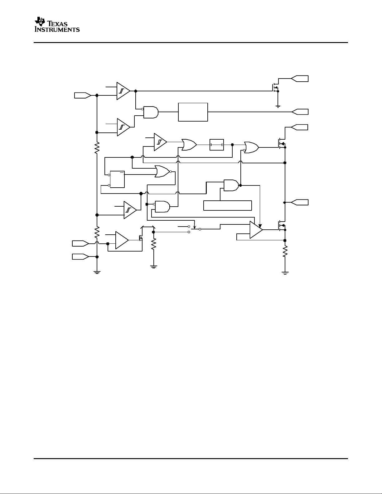
V
DD
Input
Current
V
RTN
V
Detect Classify
Power Up
and
Inrush
Class 3
(PG-RTN)
Note: All Voltages With Respect to VSS.
Current
RX
Pair
TPS2375-1
SMAJ58A
0.1 F, 100 V, 10%m
24.9 kW
1%
VDD
VSS
CLASS
DET
RTN
PG
100 kW
(2)
1
3
6
4
5
7
8
TO DC/DC
CONVERTER
ILIM
178 kW
1%
2
RJ-45
DF01S
2 Places
Data to
Ethernet PHY
Data to
Ethernet PHY
R
DET
R
CLASS
357
1%
W
(1)
R
ILIM
47 F,m
100 V
Notes:
1) Class 3 PD depicted
2) PG pullup resistor is optional.
TX
Pair
Spare
Pair
Spare
Pair
TPS2375-1
TPS2377-1
SLVS570 – MARCH 2005
IEEE 802.3af PoE POWERED DEVICE CONTROLLERS WITH AUTO-RETRY
FEATURES APPLICATIONS
• Auto-Retry After Current-Limit Fault
• TPS2375-1: IEEE 802.3af Thresholds
• TPS2377-1: Legacy Thresholds
• Fully Supports IEEE 802.3af Specification
• Integrated 0.58- Ω , 100-V, Low-Side Switch
• 15-kV System Level ESD Capable
• Programmable Inrush Current Control
• Fixed 450-mA Current Limit
• Open-Drain, Power-Good Reporting
• Industrial Temperature Range: -40 ° C to 85 ° C
• 8-Pin SOIC and TSSOP Packages
DESCRIPTION
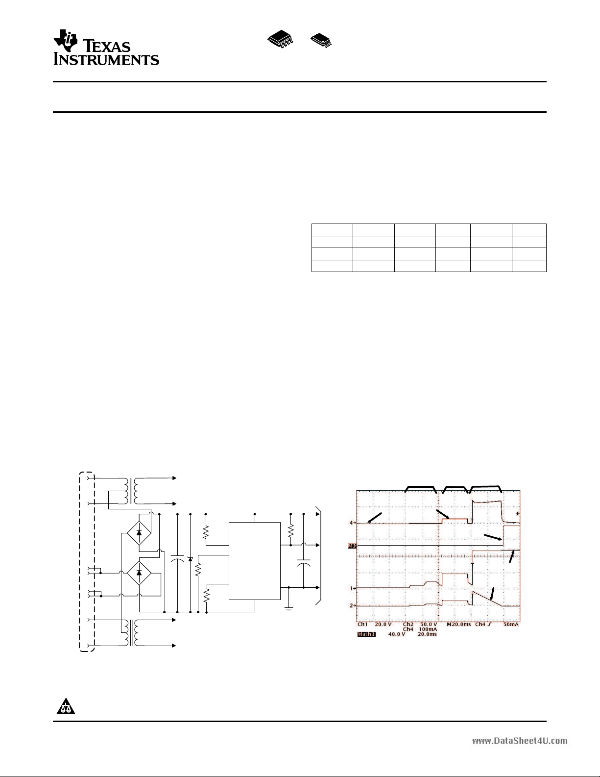
These easy-to-use 8-pin integrated circuits contain all of the features needed to develop an IEEE
802.3af-compliant powered device (PD). The TPS2375-1 and TPS2377-1 are second generation PDCs (PD
Controllers) featuring a 100-V ratings and true open-drain, power-good function. These devices are auto-retry
versions of selected TPS2375 family members. Information on the TPS2375/6/7 devices can be found on the
TPS2375/6/7 data sheet (SLVS525A ).
In addition to the basic functions of detection, classification, and undervoltage lockout (UVLO), these controllers
include an adjustable inrush limiting feature. The TPS2375-1 has 802.3af-compliant UVLO limits, and the
TPS2377-1 has legacy UVLO limits.
The TPS2375 family specifications incorporate a voltage offset of 1.5 V between its limits and the IEEE 802.3af
specifications to accommodate the required input diode bridges used to make the PD polarity insensitive.
• VoIP Phones
• WLAN Access Points
• Security Cameras
• Internet Appliances
• POS Terminals
PRODUCT SELECTOR
2375-1 2377-1 2375 2376 2377
UVLO 802.3af Legacy 802.3af Adjustable Legacy
Protection Auto-Retry Auto-Retry Latch Latch Latch
Package PW D D, PW D,PW D,PW
Additional resources can be found on the TI Web site www.ti.com.
Please be aware that an important notice concerning availability, standard warranty, and use in critical applications of Texas Instruments semiconductor products and disclaimers thereto appears at the end of this data sheet.
PRODUCTION DATA information is current as of publication date.
Products conform to specifications per the terms of the Texas
Instruments standard warranty. Production processing does not
necessarily include testing of all parameters.
Figure 1. Typical Application Circuit and Start-Up Waveforms
Copyright © 2005, Texas Instruments Incorporated
www.ti.com
TPS2375-1
TPS2377-1
SLVS570 – MARCH 2005
This integrated circuit can be damaged by ESD. Texas Instruments recommends that all integrated
circuits be handled with appropriate precautions. Failure to observe proper handling and installation
procedures can cause damage.
ESD damage can range from subtle performance degradation to complete device failure. Precision
integrated circuits may be more susceptible to damage because very small parametric changes could
cause the device not to meet its published specifications.
AVAILABLE OPTIONS
T
A
-40 ° C to 85 ° C
(1) Add an R suffix to the device type for tape and reel.
UVLO THRESHOLDS (NOMINAL) PACKAGE
TYPE LOW HIGH SO-8 TSSOP-8
802.3af 30.5 V 39.3 V -- TPS2375PW-1 2375-1
Legacy 30.5 V 35.1 V TPS2377D-1 -- 2377-1
ABSOLUTE MAXIMUM RATINGS
over operating free-air temperature range (unless otherwise noted)
VDD, RTN, DET, PG
Voltage ILIM, UVLO -0.3 V to 10 V
CLASS -0.3 V to 12 V
(3)
RTN
Current, sinking PG 0 to 5 mA
DET 0 to 1 mA
Current, sourcing
ESD Charged device model 500 V
T
J
T
stg
(1) Stresses beyond those listed under “absolute maximum ratings” may cause permanent damage to the device. These are stress ratings
only, and functional operation of the device at these or any other conditions beyond those indicated under “recommended operating
conditions” is not implied. Exposure to absolute–maximum–rated conditions for extended periods may affect device reliability.
(2) I
(3) SOA limited to V
(4) Surges applied to RJ-45 of Figure 1 between pins of RJ-45, and between pins and output voltage rails per EN61000-4-2, 1999.
= 0
(RTN)
Maximum junction temperature range Internally limited
Storage temperature range -65 ° C to 150 ° C
Lead temperature 1,6 mm (1/16 inch) from case for 10 seconds - Green Packages 260 ° C
Lead temperature 1,6 mm (1/16 inch) from case for 10 seconds - Nongreen 235 ° C
Packages
(RTN)
= 80 V and I
= 515 mA.
(RTN)
CLASS 0 to 50 mA
ILIM 0 to 1 mA
Human body model 2 kV
System level (contact/air) at RJ-45
(1)
, voltages are referenced to V
(2)
(4)
(1)
(VSS)
TPS237x
-0.3 V to 100 V
0 to 515 mA
8/15 kV
MARKING
DISSIPATION RATING TABLE
PACKAGE
D (SO-8) 238 150 266
PW (TSSOP-8) 258.5 159 251
(1) Tested per JEDEC JESD51. High-K is a (2 signal – 2 plane) test board and low-K is a double-sided
board with minimum pad area and natural convection.
(2) For the most current package and ordering information, see the Package Option Addendum at the
end of this document, or see the TI Web site at www.ti.com .
2
(2)
θJA(LOW-K) θJA(HIGH-K)
° C/W ° C/W
(1)
POWER RATING
TA= 85 ° C (HIGH-K)
(mW)
www.ti.com
TPS2375-1
TPS2377-1
SLVS570 – MARCH 2005
RECOMMENDED OPERATING CONDITIONS
MIN MAX UNIT
Input voltage range
Operating current range (sinking) RTN 0 350 mA
(1)
(1)
R
(ILIM)
Classification resistor
Inrush limit program resistor
Sinking current PG 0 2 mA
T
Operating junction temperature -40 125 ° C
J
T
Operating free–air temperature -40 85 ° C
A
(1) Voltage should not be externally applied to CLASS and ILIM.
ELECTRICAL CHARACTERISTICS
V
= 48 V, R
(VDD)
currents are into pins. Typical values are at 25 ° C. All voltages are with respect to VSS unless otherwise noted.
DETECTION
CLASSIFICATION
I
(CLASS)
V
(CL_ON)
V
(CU_OFF)
V
(CU_H)
PASS DEVICE
r
DS(on)
I
(LIM)
(1) Classification is tested with exact resistor values. A 1% tolerance classification resistor ensures compliance with IEEE 802.3af limits.
(2) This parameter specifies the RTN current value, as a percentage of the steady state inrush current, below which it must fall to make PG
assert (open-drain).
= 24.9 k Ω , R
(DET)
(CLASS)
PARAMETER TEST CONDITIONS MIN TYP MAX UNIT
Offset current 0.3 3 µA
Sleep current 4 12 µA
DET leakage current V
Detection current
Classification current
(1)
Classification lower threshold Regulator turns on, V
Classification upper threshold
Leakage current V
On resistance I
Leakage current V
Current limit V
Inrush limit V
Inrush current termination
(2)
Current rise time into inrush I
Current limit response time µs
Leakage current, ILIM V
VDD, PG, RTN 0 57 V
UVLO 0 5 V
CLASS 255 4420 Ω
62.5 500 k Ω
= 255 Ω , R
DET open, V
I
(VDD)
DET open, V
I
(VDD)
(DET)
V
(RTN)
R
(DET)
measure I
I
(DET)
R
(CLASS)
R
(CLASS)
R
(CLASS)
R
(CLASS)
R
(CLASS)
Regulator turns off, V
Hysteresis 0.5 0.78 1 V
(CLASS)
(RTN)
(VDD)
(RTN)
(RTN)
V
(RTN)
state → normal operation
R
(ILIM)
(RTN)
past upper UVLO
Apply load ∞ Ω → 20 Ω , time measured to 2 2.5
I
(RTN)
(VDD)
= 178 k Ω , and –40 ° C ≤ TJ≤ 125 ° C, unless otherwise noted. Positive
(ILIM)
= V
(VDD)
+ I
(RTN)
(VDD)
+ I
(RTN)
= V
(VDD)
= V
, V
(VDD)
= 24.9 k Ω ,
(VDD)
= 4420 Ω , 13 ≤ V
= 953 Ω , 13 ≤ V
= 549 Ω , 13 ≤ V
= 357 Ω , 13 ≤ V
= 255 Ω , 13 ≤ V
= 0 V, V
= 57 V, measure I
+ I
(VDD)
= 1.9 V, measure
(RTN)
= V
= 10.1 V, measure
(RTN)
(DET)
= 1.4 V 53.7 56 58.3 µA
(VDD)
+
(RTN)
V
= 10.1 V 395 410 417 µA
(VDD)
≤ 21 V 2.2 2.4 2.8
(VDD)
≤ 21 V 10.3 10.6 11.3
(VDD)
≤ 21 V 17.7 18.3 19.5 mA
(VDD)
≤ 21 V 27.1 28 29.5
(VDD)
≤ 21 V 38 39.4 41.2
(VDD)
rising 10.2 11.3 13.0 V
(VDD)
rising 21 21.9 23 V
(VDD)
0.1 5 µA
= 57 V 1 µA
= 300 mA 0.58 1.0 Ω
= V
= 30 V 15 µA
(RTN)
= 1 V 405 461 515 mA
= 2 V, R
falling, R
= 69.8 k Ω , V
= 30 mA → 300 mA, V
= 178 k Ω 100 130 180 mA
(ILIM)
= 178 k Ω , inrush 85% 91% 100%
(ILIM)
= 5 V, 15 25
(RTN-VSS)
increasing µs
(VDD)
= 45 mA
= 15 V, V
= 0 V 1 µA
(UVLO)
3
www.ti.com
TPS2375-1
TPS2377-1
SLVS570 – MARCH 2005
ELECTRICAL CHARACTERISTICS (continued)
V
= 48 V, R
(VDD)
currents are into pins. Typical values are at 25 ° C. All voltages are with respect to VSS unless otherwise noted.
PG
UVLO
V
(UVLO_R)
V
(UVLO_F)
THERMAL SHUTDOWN
BIAS CURRENT
(DET)
= 24.9 k Ω , R
= 255 Ω , R
(CLASS)
= 178 k Ω , and –40 ° C ≤ TJ≤ 125 ° C, unless otherwise noted. Positive
(ILIM)
PARAMETER TEST CONDITIONS MIN TYP MAX UNIT
Voltage threshold rising
(3)
V
rising 9.5 10 10.5 V
(RTN)
PG deglitch Delay rising and falling PG 75 150 225 µs
I
Output low voltage
Leakage current V
TPS2375 Voltage at VDD V
= 2 mA, V
(PG)
V
= 38 V, V
(VDD)
I
= 2 mA, V
(PG)
= 57 V, V
(PG)
V
rising 38.4 39.3 40.4
(VDD)
falling 29.6 30.5 31.5 V
(VDD)
= 34 V, 0.12 0.4
(RTN)
falling
(RTN)
= 0 V, V
(RTN)
= 0 V 0.1 1 µA
(RTN)
= 25 V 0.12 0.4 V
(VDD)
Hysteresis 8.3 8.8 9.1
V
rising 34.1 35.1 36.0
(VDD)
TPS2377 Voltage at VDD V
falling 29.7 30.5 31.4 V
(VDD)
Hysteresis 4.3 4.5 4.8
Shutdown temperature Temperature rising 135 ° C
Hysteresis 20 ° C
Operating current I
(VDD)
V
240 450 µA
(3) Start with V
= 0 V, then increase V
(RTN)
until PG switches. Measure before thermal shutdown occurs.
(RTN)
4
www.ti.com
DEVICE INFORMATION
-
+
10-V
Regulator
Thermal Shutdown
QS
R
-
+
-
+
3
2
12 V
22 V
1.5 V
& 10 V
2.5 V
-
+
VDD
RTN
45 mV
CLASS
DET
Current
Limit Amp.
UVLO
Comp.
EN
Delay
5
8
6
PG
-
+
1 = Inrush
1 = Limiting
PG Comparator
Detection
Comparator
Classification
Comparator
0
1
-
+
2.5 V
1
ILIM
1:1
4
VSS
Current
Mirror
1 kW
0.08 W
150 Sm
FUNCTIONAL BLOCK DIAGRAM
TPS2375-1
TPS2377-1
SLVS570 – MARCH 2005
5
www.ti.com
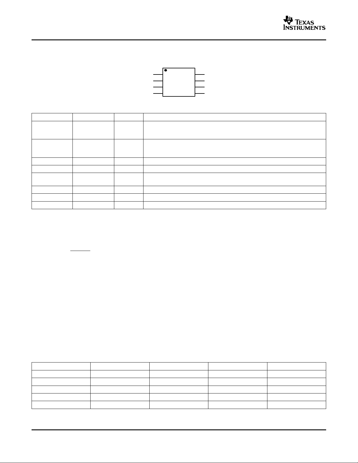
1
2
3
4
5
6
7
8
VSS
CLASS
N/C
DET
RTN
PG
VDD
ILIM
I
(LIM)
25000
R
(ILIM)
TPS2375-1
TPS2377-1
SLVS570 – MARCH 2005
DEVICE INFORMATION (continued)
TPS2375-1/77-1
(TOP VIEW)
TERMINAL FUNCTIONS
PIN NAME PIN NUMBER I/O DESCRIPTION
ILIM 1 O equation for calculating the resistor is shown in the detailed pin description section for
CLASS 2 O (PD). The IEEE classification levels and corresponding resistor values are shown in
DET 3 O Connect a 24.9-k Ω detection resistor from DET to VDD for a valid PD detection.
VSS 4 I Return line on the source side of the TPS2375-1 from the PSE.
RTN 5 O
PG 6 O Open-drain, power-good output; active high.
NC 7 No connection
VDD 8 I Positive line from the rectified PSE provided input.
Connect a resistor from ILIM to VSS to set the start-up inrush current limit. The
ILIM.
Connect a resistor from CLASS to VSS to set the classification of the powered device
Table 1 .
Switched output side return line used as the low-side reference for the TPS2375-1
load.
Detailed Pin Description
The following descriptions refer to the schematic of Figure 1 and the functional block diagram.
ILIM: A resistor from this pin to VSS sets the inrush current limit per Equation 1 :
where ILIM is the desired inrush current value, in amperes, and R
from ILIM to VSS, in ohms. The practical limits on R
are 62.5 k Ω to 500 k Ω . A value of 178 k Ω is
(ILIM)
recommended for compatibility with legacy power sourcing equipment (PSE).
Inrush current limiting prevents current drawn by the bulk capacitor from causing the line voltage to sag below
the lower UVLO threshold. Adjustable inrush current limiting allows the use of arbitrarily large capacitors and also
accommodates legacy systems that require low inrush currents.
The ILIM pin must not be left open or shorted to VSS.
CLASS: Classification is implemented by means of an external resistor, R
and VSS. The controller draws current from the input line through R
13 V and 21 V. The classification currents specified in the electrical characteristics table include the bias current
flowing into VDD and any RTN leakage current.
Table 1. CLASSIFICATION
CLASS PD POWER (W) R
0 0.44 – 12.95 4420 ± 1% 0 - 4 Default class
1 0.44 – 3.84 953 ± 1% 9 - 12
2 3.84 – 6.49 549 ± 1% 17 - 20
3 6.49 – 12.95 357 ± 1% 26 - 30
4 - 255 ± 1% 36 - 44 Reserved for future use
( Ω ) 802.3af LIMITS (mA) NOTE
(CLASS)
is the value of the programming resistor
(ILIM)
, connected between CLASS
(CLASS)
(CLASS)
when the input voltage lies between
(1)
6

www.ti.com
TPS2375-1
TPS2377-1
SLVS570 – MARCH 2005
The CLASS pin must not be shorted to ground.
DET: Connect a resistor, R
applications. R
is connected across the input line when V
(DET)
disconnected when the line voltage exceeds this range to conserve power. This voltage range has been chosen
to allow detection with two silicon rectifiers between the controller and the RJ-45 connector.
VSS: This is the input supply negative rail that serves as a local ground.
RTN: This pin provides the switched negative power rail used by the downstream circuits. The operational and
inrush current limit control current into the pin. The PG circuit monitors the RTN voltage and also uses it as the
return for the PG pin pulldown transistor. The internal MOSFET body diode clamps VSS to RTN when voltage is
present between VDD and RTN and the Power-over-Ethernet (PoE) input is not present.
PG: This pin goes to a high resistance state when the internal MOSFET that feeds the RTN pin is enabled, and
the device is not in inrush current limiting. In all other states except detection, the PG output is pulled to RTN by
the internal open-drain transistor. Performance is ensured with at least 4 V between VDD and RTN.
PG is an open-drain output; therefore, it may require a pullup resistor or other interface.
VDD: This is the positive input supply that is also common to downstream load circuits. This pin provides
operating power and allows the controller to monitor the line voltage to determine the mode of operation.
, between DET and VDD. This resistor should equal 24.9 k Ω , ± 1% for most
(DET)
lies between 1.4 V and 11.3 V, and is
(VDD)
7

www.ti.com
11.0
11.1
11.2
11.3
−40 −20 0 20 40 60 80 100 120
Classification Turnon Voltage − V
TA − Free-Air Temperature − °C
0
1
2
3
4
5
6
0 1 2 3 4 5 6 7 8 9 10 11
TA = 125°C
TA = 25°C
TA = −40°C
V
(VDD)
− V
Current − Aµ
10
15
20
25
30
35
1 3 5 7 9 11
Specification Limits
V
(PI)
− V
Resistance − kΩ
21.90
21.91
21.92
21.93
21.94
−40 −20 0 20 40 60 80 100 120
Classification Turnoff Voltage − V
TA − Free-Air Temperature − °C
0.100
0.150
0.200
0.250
0.300
0.350
22 27 32 37 42 47 52 57
VDD − V
I
(VDD)
− mA
TA = 125°C
TA = 25°C
TA = −40°C
0.4
0.5
0.6
0.7
0.8
0.9
−40 −20 0 20 40 60 80 100 120
Pass Device Resistance − Ω
TA − Free-Air Temperature − °C
TPS2375-1
TPS2377-1
SLVS570 – MARCH 2005
TYPICAL CHARACTERISTICS
Graphs over temperature are interpolations between the marked data points.
PD DETECTION RESISTANCE VOLTAGE
CLASSIFICATION TURNON
vs vs
I
+ I
(VDD)
IN DETECTION V
(RTN)
(PI)
Figure 2. Figure 3. Figure 4.
CLASSIFICATION TURNOFF PASS DEVICE
VOLTAGE I
vs vs vs
CURRENT RESISTANCE
(VDD)
TEMPERATURE VDD TEMPERATURE
TEMPERATURE
8
Figure 5. Figure 6. Figure 7.

www.ti.com
39.2
39.3
39.4
39.5
−40 −20 0 20 40 60 80 100 120
T
A
− Free-Air Temperature − °C
VDD − V
30.40
30.44
30.48
30.52
30.56
30.60
−40 −20 0 20 40 60 80 100 120
T
A
− Free-Air Temperature − °C
VDD − V
34.95
35.00
35.05
35.10
35.15
35.20
−40 −20 0 20 40 60 80 100 120
T
A
− Free-Air Temperature − °C
VDD − V
30.45
30.50
30.55
30.60
30.65
−40 −20 0 20 40 60 80 100 120
T
A
− Free-Air Temperature − °C
VDD − V
90.5
91.0
91.5
92.0
92.5
93.0
93.5
94.0
−40 −20 0 20 40 60 80 100 120
Percent of Inrush Limit Current
TA − Free-Air Temperature − °C
100
125
150
175
200
225
250
275
300
325
350
−40 −20 0 20 40 60 80 100 120
I
(ILIM)
− mA
TA − Free-Air Temperature − °C
75 kΩ
125 kΩ
178 kΩ
425
430
435
440
−40 −20 0 20 40 60 80 100 120
T
A
− Free-Air Temperature − °C
I
(RTN)
− mA
120
140
160
180
−40 −20 0 20 40 60 80 100 120
PG Deglitch Period −
sµ
TA − Free-Air Temperature − °C
TYPICAL CHARACTERISTICS (continued)
Graphs over temperature are interpolations between the marked data points.
TPS2375-1 TPS2375-1 TPS2377-1
UVLO RISING UVLO FALLING UVLO RISING
vs vs vs
TEMPERATURE TEMPERATURE TEMPERATURE
Figure 8. Figure 9. Figure 10.
TPS2375-1
TPS2377-1
SLVS570 – MARCH 2005
TPS2377-1 INRUSH STATE TERMINATION
UVLO FALLING THRESHOLD INRUSH CURRENT
vs vs vs
TEMPERATURE TEMPERATURE TEMPERATURE
Figure 11. Figure 12. Figure 13.
CURRENT LIMIT PG DEGLITCH PERIOD
vs vs
TEMPERATURE TEMPERATURE
Figure 14. Figure 15.
9
www.ti.com
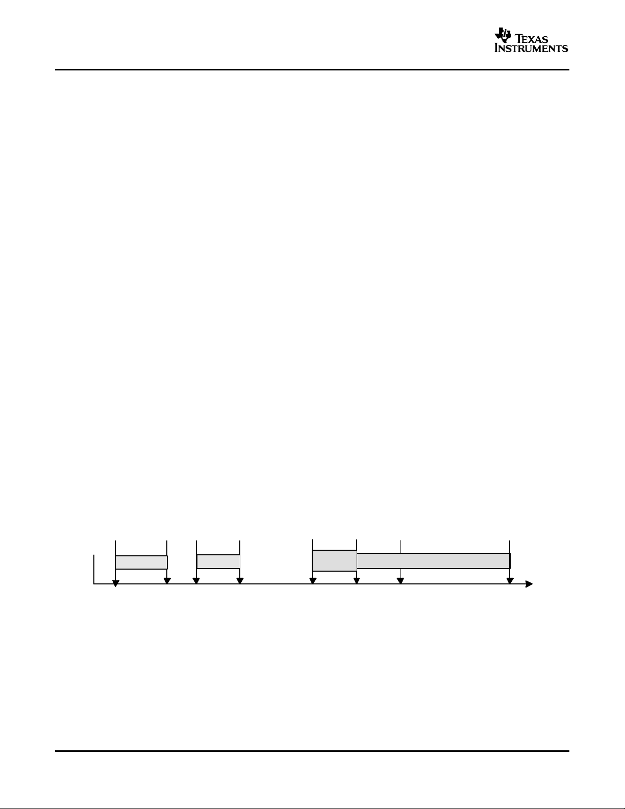
Normal Operation
57
42
363020.514.510.12.7
Detection
Lower Limit
Detection
Upper Limit
Classification
Lower Limit
Classification
Upper Limit
Must Turn Off by −
Voltage Falling
Lower Limit −
Proper Operation
Must Turn On by−
Voltage Rising
Maximum Input
Voltage
Detect
Classify
Shut -
down
PI Voltage (V)
0
TPS2375-1
TPS2377-1
SLVS570 – MARCH 2005
APPLICATION INFORMATION
OVERVIEW
The IEEE 802.3af specification defines a process for safely powering a powered device (PD) over a cable, and
then removing power if a PD is disconnected. The process proceeds through three operational states: detection,
classification, and operation. The intent behind the process is to leave an unterminated cable unpowered while
the PSE periodically checks for a plugged-in device; this is referred to as detection. The low power levels used
during detection are unlikely to cause damage to devices not designed for PoE. If a valid PD signature is
present, then the PSE may optionally inquire how much power the PD requires; this is referred to as
classification. The PD may return a default full-power signature, or one of four other choices. Knowing the power
demand of each PD allows the PSE to intelligently allocate power between PDs, and also to protect itself against
overload. The PSE powers up a valid PD, and then monitors its output for overloads. The maintain power
signature (MPS) is presented by the powered PD to assure the PSE that it is there. The PSE monitors its output
for the MPS to see if the PD is removed, and turns the port off, if it loses the MPS. Loss of MPS returns the PSE
to the initial state of detection. Figure 16 shows the operational states as a function of PD input voltage range.
The PD input is typically an RJ-45 (8-pin) connector, referred to as the power interface (PI). PD input
requirements differ from PSE output requirements to account for voltage drops in the cable and margin. The
specification uses a cable resistance of 20 Ω to derive the voltage limits at the PD from the PSE output
requirements. Although the standard specifies an output power of 15.4 W at the PSE output, there is only
12.95 W available at the input of the PD due to the worst-case power loss in the cable.
The PSE can apply voltage either between the RX and TX pairs, or between the two spare pairs as shown in
Figure 1 . The applied voltage can be of either polarity. The PSE cannot apply voltage to both paths at the same
time. The PD uses input diode bridges to accept power from any of the possible PSE configurations. The voltage
drops associated with the input bridges cause a difference between the IEEE 802.3af limits at the PI and the
TPS2375-1 specifications.
The PSE is required to current limit between 350 mA and 400 mA during normal operation, and it must
disconnect the PD if it draws this current for more than 75 ms. The PSE may set lower output current limits
based on the PD advertised power requirements, as discussed in the Classification section.
The following discussion is intended as an aid in understanding the operation of the TPS2375-1, but not as a
substitute for the actual IEEE 802.3af standard. Standards change and should always be referenced when
making design decisions.
Figure 16. IEEE 802.3 PD Limits
INTERNAL THRESHOLDS
In order to implement the PoE functionality as shown in Figure 16 , the TPS2375-1 has a number of internal
comparators with hysteresis for stable switching between the various states. Figure 17 relates the parameters in
the Electrical Characteristics section to the PoE states. The mode labeled idle between classification and
detection implies that the DET, CLASS, PG, and RTN pins are all high impedance.
10

www.ti.com
Operational Mode
Detection
Classification
PD Powered
Idle
1.4V
V
(CL_ON)
V
(CU_OFF)
V
(CU_H)
V
(UVLO_F)
V
(UVLO_R)
V
(VDD)
TPS2375-1
TPS2377-1
SLVS570 – MARCH 2005
APPLICATION INFORMATION (continued)
Figure 17. Threshold Voltages
DETECTION
This feature of IEEE 802.3af eliminates powering and potentially damaging Ethernet devices not intended for
application of 48 V. When a voltage in the range of 2.7 V to 10.1 V is applied to the PI, an incremental resistance
of 25 k Ω signals the PSE that the PD is capable of accepting power. A PD that is capable of accepting power,
but is not ready, may present an incorrect signature intentionally. The incremental resistance is measured by
applying two different voltages to the PI and measuring the current it draws. These two test voltages must be
within the specified range and be at least 1 V apart. The incremental resistance equals the difference between
the voltages divided by the difference between the currents. The allowed range of resistance is 23.75 k Ω to
26.25 k Ω .
The TPS2375-1 is in detection mode whenever the supply voltage is below the lower classification threshold. The
TPS2375-1 draws a minimum of bias power in this condition, while PG and RTN are high impedance and the
circuits associated with ILIM and CLASS are disabled. The DET pin is pulled to ground during detection. Current
flowing through R
resistor is recommended. R
When the input voltage rises above the 11.3 V lower classification comparator threshold, the DET pin goes to an
open-drain condition to conserve power.
The input diode bridge incremental resistance can be hundreds of ohms at the low currents seen at 2.7 V on the
PI. The bridge resistance is in series with R
with the type of diode selected by the designer, and it is not usually specified on the diode data sheet. The value
of R
may be adjusted downwards to accommodate a particular diode type.
(DET)
to VSS ( Figure 1 ) produces the detection signature. For most applications, a 24.9-k Ω , 1%,
(DET)
can be a small, low-power resistor because it only sees a stress of about 5 mW.
(DET)
and increases the total resistance seen by the PSE. This varys
(DET)
CLASSIFICATION
Once the PSE has detected a PD, it may optionally classify the PD. This process allows a PSE to determine the
PD power requirements in order to allot only as much power as necessary from its fixed input power source. This
allows the PSE to power the maximum number of PDs from a particular power budget. This step is optional
because some PSEs can afford to allot the full power to every powered port.
The classification process applies a voltage between 14.5 V and 20.5 V to the input of the PD, which in turn
draws a fixed current set by R
classes ( Table 1 ) that the PD is signalling. The total current drawn from the PSE during classification is the sum
of bias currents and current through R
classification range to avoid excessive power dissipation ( Figure 16 and Figure 17 ).
The value of R
requirements of the PD. The power rating of this resistor should be chosen so that it is not overstressed for the
required 75-ms classification period, during which 10 V is applied. The PD could be in classification for extended
periods during bench test conditions, or if an auxiliary power source with voltage within the classification range is
connected to the PD front end. Thermal protection may activate and turn classification off if it continues for more
than 75 ms, but the design must not rely on this function to protect the resistor.
(CLASS)
. The PSE measures the PD current to determine which of the five available
(CLASS)
. The TPS2375-1 disconnects R
(CLASS)
(CLASS)
should be chosen from the values listed in Table 1 based on the average power
at voltages above the
11

www.ti.com
TPS2375-1
TPS2377-1
SLVS570 – MARCH 2005
APPLICATION INFORMATION (continued)
UNDERVOLTAGE LOCKOUT (UVLO)
The TPS2375-1 incorporates an undervoltage lockout (UVLO) circuit that monitors line voltage to determine
when to apply power to the downstream load and allow the PD to power up. The IEEE 802.3af specification
dictates a maximum PD turnon voltage of 42 V and a minimum turnoff voltage of 30 V ( Figure 17 ). The IEEE
802.3af standard assumes an 8-V drop in the cabling based on a 20- Ω feed resistance and a 400-mA maximum
inrush limit. Because the minimum PSE output voltage is 44 V, the PD must continue to operate properly with
input voltages as low as 36 V. The TPS2375-1 UVLO limits are designed to meet the turnon, turnoff, and
hysteresis requirements.
Various legacy PSE systems in the field do not meet the minimum output voltage of 44 V. The TPS2377-1 UVLO
limits are designed to support these systems with a lower turnon voltage and smaller hysteresis. Although the
TPS2377-1 works with compliant PSEs, it could potentially exhibit startup instabilities if the PSE output voltage
rises slowly. The TPS2375-1 is recommended for applications with compliant PSEs.
The TPS2375-1 uses the UVLO function to control the load through an integrated MOSFET switch. Figure 17
graphically shows the relationships of the UVLO thresholds defined in the Electrical Characteristics section to the
TPS2375-1 operational states.
PROGRAMMABLE INRUSH CURRENT LIMIT AND FIXED OPERATIONAL CURRENT LIMIT
Inrush limiting has several benefits. First, it provides a mechanism to keep the inrush current below the 400 mA,
50 ms, maximum inrush allowed by the standard. Second, by keeping the current below the PSE operational
limit, which can be as low as the classification power divided by the PSE voltage, it allows an arbitrarily
large-bulk capacitor to be charged. Third, some legacy PSEs may not tolerate large inrush currents while
powering their outputs up.
The TPS2375-1 operational current limit protects the internal power switch from sudden output faults and current
surges. The minimum operational current limit level of 405 mA lies above the maximum PSE output current limit
of 400 mA. This current limit enables the PD to draw the maximum available power and also allows the PSE to
detect fault conditions. The IEEE 802.3af standard allows PDs to draw momentary currents up to 400 mA, which
can be prevented if the current limit is set lower.
The TPS2375-1 incorporates a state machine that controls the inrush and operational current limit states. When
V
is below the lower UVLO threshold, the current limit state machine is reset. In this condition, the RTN pin
(VDD)
is high impedance, and floats to V
UVLO turnon threshold, the TPS2375-1 enables the internal power MOSFET with the current limit set to the
value programmed by R
V
. Once the inrush current falls about 10% below the programmed limit for 150-µs, the current limit switches
(VSS)
. The load capacitor charges and the RTN pin voltage falls from V
(ILIM)
to the 450-mA operational level and PG goes open-drain. This switchover is seen in the operation of PG in
Figure 1 . The internal power MOSFET is disabled if the input voltage drops below the lower UVLO threshold and
the state machine is reset
The inrush limit, bulk capacitor size, and downstream dc/dc converter startup method must be chosen so that the
converter input current does not exceed the inrush current limit while it is active. This is achieved by using the
PG output to enable the downstream converter after inrush finishes, by delaying the converter startup until inrush
finishes, or by increasing the value of the inrush current limit.
Practical values of R
lie between 62.5 k Ω and 500 k Ω ; however, selecting lower inrush current values
(ILIM)
reduces peak stresses under output-short circuit conditions. An inrush level of 140 mA, set by an R
k Ω , is used with TPS2377 applications for compatibility with legacy systems. This same inrush current level is
recommended for most TPS2375 applications, and it should be kept below 250 mA if the application allows.
once the output capacitor is discharged. When V
(VDD)
(VDD)
rises above the
to nearly
(VDD)
(ILIM)
of 178
PROTECTION OPERATION
The TPS2375-1 protects itself, the load, and the PSE using a number of mechanisms while the input voltage is
above the lower UVLO. This operation is illustrated by considering the cases of soft overload, hard overload, and
input-voltage steps.
A soft overload is one that forces the internal MOSFET into current limit with V
(RTN-VSS)
less than 10 V. Provided
that the PSE does not respond to this event, the bulk capacitor recharges after a momentary overload, and
operation returns to normal. If the overload persists, the TPS2375-1 may overheat and go into thermal shutdown
12

www.ti.com
TPS2375-1
TPS2377-1
SLVS570 – MARCH 2005
APPLICATION INFORMATION (continued)
because of the large thermal dissipation, which may be as high as 4.5 W. The MOSFET is turned off, and PG
goes low, until the die cools and the MOSFET is re-enabled. If V
(RTN-VSS)
current limit remains at 450 mA and PG goes open-drain. If the overload has caused V
while the MOSFET was disabled, then the current limit is set to the inrush level and PG remains low.
Downstream converters that use PG control are turned off, permitting a normal start cycle. Converters that do not
use PG need to allow a restart by either drawing less current than the inrush current limit provides, or by
disabling long enough to allow the bulk capacitor to recharge. A converter that has bootstrap startup can be
designed to accomplish this goal.
A hard overload is one that forces the internal MOSFET into current limit with V
µ s. The MOSFET current limit switches to inrush level and PG goes low. Switching to the inrush current limit
under this condition reduces the stress to the TPS2375-1, other PD components, and the PSE. The peak power
dissipated depends on the inrush current programmed using the ILIM pin, which is the basis of choosing lower
current limits per the preceding recommendations. If the overload persists, the TPS2375-1 begins to thermally
cycle. The bulk capacitor recharges with a normal start cycle if the overload is removed, and the PD recovers.
The same comments about converter control with PG and restart apply.
Another possible condition is a rapid input voltage rise to the PD. The TPS2375-1 is forced into current limit
when the capacitor charges to the higher voltage, while also supplying the load. If the step voltage is small
enough, the capacitor recharges and operation is unaffected. If the load demand is close to the current limit, and
a large bulk capacitor is used, then thermal limit can be triggered. If V
limit drops to the inrush value and PG goes open-drain. Recovery occurs as previously discussed.
is less than 10 V when re-enabled, the
(RTN-VSS)
(RTN-VSS)
(RTN-VSS)
is greater than 10 V, the current
greater than 10 V for 150
to exceed 10 V
FAULT CONDITIONS IN TPS2375-1 vs. TPS2375
The TPS2375-1 uses the current limit, internal thermal shutdown, and foldback to inrush to protect itself, the
load, and the PSE during normal operation. The TPS2375-1 does not latch off under these fault conditions. By
contrast, the TPS2375 does latch off after eight overtemperature cycles, or after an overload or input transient
causes the voltage across the pass MOSFET to exceed 10 V for 150 µ s. The TPS2375-1 automatically restarts
the PD if the load fault is removed or after a source transient, such as a voltage dropout. The TPS2375 provides
the best protection for itself, the load, and the PSE while the TPS2375-1 provides automatic recovery under
adverse conditions.
The TPS2375-1 satisfies system designs that require hotswap which automatically restarts after prolonged
overload or input voltage transients. In addition to differences in protection, there is a difference in how a PSE
handles the different devices. A PSE using dc MPS interprets a latched-off device as PD removal due to loss of
MPS, and recycles the input power. PSEs with ac MPS may interpret the latched-off PD impedance as
operational, and continue power. This operation is subject to wide variation due to the excessive range allowed in
the IEEE 802.3af standard. A continually cycling PD satisfies PSEs with both ac and dc MPS that the PD is
present, and the PSE does not have an indication that there is a problem with the PD.
MAINTAIN POWER SIGNATURE
Once a valid PD has been detected and powered, the PSE uses the maintain power signature (MPS) to
determine when to remove power from the PI. The PSE removes power from that output port if it detects loss of
MPS for 300 ms or more. A valid MPS requires the PD to draw at least 10 mA and also have an ac impedance
less than 26.25 k Ω in parallel with 0.05 µF. TI's reference designs meet the requirements necessary to maintain
power.
POWER GOOD
The TPS2375-1 includes a power-good circuit that can be used to signal the PD circuitry that the load capacitor
is fully charged. This pin is intended for use as an enable signal for downstream circuitry. If the converter tries to
start up while inrush is active, and draws a current equal to the inrush limit, a latchup condition occurs in which
the PD never successfully starts. Using the PG pin is the safest way to ensure that there are no undesired
interactions between the inrush limit, the converter startup characteristic, and the size of the bulk capacitor.
13

www.ti.com
TPS2375-1
TPS2377-1
SLVS570 – MARCH 2005
APPLICATION INFORMATION (continued)
The PG pin goes to an open-drain state approximately 150 µs after the inrush current falls 10% below the
regulated value. PG pulldown current is only ensured when the voltage difference between VDD and RTN
exceeds 4 V. This is not a limiting factor because the dc/dc converter should not be able to run from 4 V. The PG
output is pulled to RTN whenever the MOSFET is disabled, is in inrush current limiting, or the voltage rises
above 10 V.
Referencing PG to RTN simplifies the interface to the downstream dc/dc converter or other circuit because it is
referenced to RTN, not VSS. Care must be used in interfacing the PG pin to the downstream circuits. The pullup
to VDD shown in Figure 1 may not be appropriate for a particular dc/dc converter interface. The PG pin connects
to an internal open-drain, 100-V transistor capable of sinking 2 mA to a voltage below 0.4 V. The PG pin can be
left open if it is not used.
THERMAL PROTECTION
The controller may overheat after operation in inrush current-limit, or classification for an extended period of time,
or if the ambient temperature becomes excessive. The TPS2375-1 protects itself by disabling the RTN and
CLASS pins when the internal die temperature reaches about 140 ° C. It automatically restarts when the die
temperature has fallen approximately 20 ° C. This process is referred to as thermal cycling. Thermal protection is
active whenever the TPS2375 is not in detection.
Many PSEs do not recognize, and deactivate, a PD that fails with a short beyond the TPS2375-1, because the
MPS criteria are satisfied. The TPS2375-1 continues thermal cycles under this condition to protect itself and
other downstream components that repeatedly exceed the recommended junction temperature of 125 ° C. Short
periods of thermal cycling do not significantly impact the reliability or life expectancy, but prolonged periods may.
Other components in the power path can be overstressed if this condition exists for a prolonged time as well.
Additional protection for parts that cannot take the repetitive overstress is provided by the TPS2375 with latch-off.
POWER SYSTEM DESIGN
The PSE is a power and current limited source, which imposes certain constraints on the PD power supply
design. DC/DC converters have both a constant input power characteristic that causes them to draw high
currents at low voltage, and they tend to go to a full input power mode during start-up that is often 25% or more
above their rated power. Improper design of the power system can cause the PD to not start up with all
combinations of Ethernet lines and PSE sources.
The following guidelines should be used:
1. Set the TPS2375-1 inrush to a moderate value as previously discussed.
2. Hold the dc/dc converter off during inrush as previously discussed.
3. The converter should have a softstart that keeps the peak input start-up current below 400 mA, and
preferably only a modest amount over the operating current, with a 44-V PSE source and a 20- Ω loop.
4. If step 3 cannot be met, the bulk input capacitor should not discharge more than 8 V during converter
start-up from a 400-mA limited, 44-V source with a 20- Ω line. Start-up must be completed in less than 50 mS
Step 4 requires a balance between the converter output capacitance, load, and input bulk capacitance. While
there are some cases which may not require all these measures, such as a 1-W PD with minimal converter
output capacitance, it is always a good practice to follow them.
AUXILIARY POWER SOURCE ORING
Many PoE-capable devices are designed to operate from either a wall adapter or PoE power. A local power
solution adds cost and complexity, but allows a product to be used regardless of PoE availability. Attempting to
create solutions where the two power sources coexist in a specific controlled manner results in additional
complexity, and is not generally recommended. Figure 18 demonstrates three methods of diode ORing external
power into a PD. Option 1 inserts power on the output side of the PoE power conversion. Option 2 inserts power
on the TPS2375-1 output. Option 3 applies power to the TPS2375-1 input. Each of these options has
advantages and disadvantages. The wall adapter must meet a minimum 1500-Vac dielectric withstand test
voltage to the ac input power and to ground for options 2 and 3.
14

www.ti.com
TPS237X
SMAJ58A
R
(DET)
R
(CLASS)
VDDVSS
CLASS
DET
RTN
Main
DC/DC
Converter
Output
R
(ILIM)
RJ−45
Option 1
ILIM
DC/DC
Converter
UCC3809
or
UCC3813
Optional
Regulator
Option 2
Option 3
A Full Wave Bridge
Gives Flexibility To
Use Supply With Either
Polarity
For Option 2,
The Capacitor Must Be
Right At The Output
To Control The
Transients.
Auxiliary
Power
Input
Use only
one option
See TI Document SLVR030 For A Typical
Application Circuit.
~
~
+
−
~
~
+
−
0.1 µF
22 µF
Inserting a Diode in This Location
With Option 2, Allows PoE To Start
With Aux Power Present.
APPLICATION INFORMATION (continued)
TPS2375-1
TPS2377-1
SLVS570 – MARCH 2005
Figure 18. Auxiliary Power ORing
Option 1 consists of ORing power to the output of the PoE dc/dc converter. This option is preferred in cases
where PoE is added to an existing design that uses a low-voltage wall adapter. The relatively large PD
capacitance reduces the potential for harmful transients when the adapter is plugged in. The wall adapter output
may be grounded if the PD incorporates an isolated converter. This solution requires two separate regulators, but
low-voltage adapters are readily available. The PoE power can be given priority by setting its output voltage
above that from the auxiliary source.
Option 2 has the benefits that the adapter voltage may be lower than the TPS2375-1 UVLO, and that the bulk
capacitor shown can control voltage transients caused by plugging in an adapter. The capacitor size and location
are chosen to control the amount of ringing that can occur on this node, which can be affected by additional
filtering components specific to a dc/dc converter design. The optional diode blocks the adapter voltage from
reverse biasing the input, and allows a PoE source to apply power provided that the PSE output voltage is
greater than the adapter voltage. The penalty of the diode is an additional power loss when running from PSE
power. The PSE may not be able to detect and start powering without the diode. This means that the adapter
may continue to power the PD until removed. Auxiliary voltage sources can be selected to be above or below the
PoE operational voltage range. If automatic PoE precedence is desired when using the low-voltage auxiliary
source option, make sure that the TPS2375-1 inrush program limit is set higher than the maximum converter
input current at its lowest operating voltage. It is difficult to use PG with the low-voltage auxiliary source because
the converter must operate during a condition when the TPS2375-1 would normally disable it. Circuits may be
designed to force operation from one source or the other depending on the desired operation and the auxiliary
source voltage chosen. However, they are not recommended because they increase complexity and thus cost.
Option 3 inserts the power before the TPS2375-1. It is necessary for the adapter to meet the TPS2375-1 UVLO
turnon requirement and to limit the maximum voltage to 57 V. This option provides a valid power-good signal and
simplifies power priority issues. The disadvantage of this method is that it is the most likely to cause transient
voltage problems. Plugging a powered adapter in applies a step input voltage to a node that has little
capacitance to control the dv/dt and voltage ringing. If the wall mount supply applies power to the PD before the
PSE, it prevents the PSE from detecting the PD. If the PSE is already powering the PD when the auxiliary source
is plugged in, priority is given to the higher supply voltage.
15

www.ti.com
C
I
(PD)
180
10 mA
TPS2375-1
TPS2377-1
SLVS570 – MARCH 2005
APPLICATION INFORMATION (continued)
ESD
The TPS2375-1 has been tested using the surge of EN61000-4-2 in an evaluation module (EVM) using the
circuit in Figure 1 . The levels used were 8-kV contact discharge and 15-kV air discharge. Surges were applied
between the RJ-45 and the dc EVM outputs, and between an auxiliary power input jack and the dc outputs. No
failures were observed.
ESD requirements for a unit that incorporates the TPS2375-1 have much broader scope and operational
implications than those used in TI’s testing. Unit level requirements should not be confused with EVM testing that
only validated the TPS2375-1.
EXTERNAL COMPONENTS
Transformer
Nodes on an Ethernet network commonly interface to the outside world via an isolation transformer per IEEE
802.3 requirements (see Figure 1 ). For powered devices, the isolation transformer must include a center tap on
the media (cable) side. Proper termination is required around the transformer to provide correct impedance
matching and to avoid radiated and conducted emissions. Transformers must be specifically rated to work with
the Ethernet chipset, and the IEEE 802.3af standard.
Input Diodes or Diode Bridges
The IEEE 802.3af requires the PD to accept power on either set of input pairs in either polarity. This requirement
is satisfied by using two full-wave input bridge rectifiers as shown in Figure 1 . Silicon p-n diodes with a 1-A or
1.5-A rating and a minimum breakdown of 100 V are recommended. Diodes exhibit large dynamic resistance
under low-current operating conditions such as in detection. The diodes should be tested for their behavior under
this condition. The diode forward drops must be less than 1.5 V at 500 µA and at the lowest operating
temperature.
Input Capacitor
The IEEE 802.3af requires a PD input capacitance between 0.05 µF and 0.12 µ F during detection. This capacitor
should be located directly adjacent to the TPS2375-1 as shown in Figure 1 . A 100-V, 10%, X7R ceramic
capacitor meets the specification over a wide temperature range.
Load Capacitor
The IEEE 802.3af specification requires that the PD maintain a minimum load capacitance of 5 µ F. It is
permissible to have a much larger load capacitor, and the TPS2375-1 can charge in excess of 470 µF before
thermal issues become a problem. However, if the load capacitor is too large, the PD design may violate IEEE
802.3af requirements.
If the load capacitor is too large, there can be a problem with inadvertent power shutdown by the PSE caused by
failure to meet the MPS. This is caused by having a long input current dropout due to a drop in input voltage with
a large capacitance-to-load ratio. The standard gives Equation 2 :
where C is the bulk capacitance in µ F and I
is the PD load current in mA.
(PD)
A particular design may have a tendency to cause ringing at the RTN pin during startup, inadvertent hot-plugs of
the PoE input, or plugging in a wall adapter. It is recommended that a minimum value of 1 µF be used at the
output of the TPS2375-1 if downstream filtering prevents placing the larger bulk capacitor right on the output.
When using ORing option 2, it is recommended that a large capacitor such as a 22 µ F be placed across the
TPS2375-1 output.
(2)
16

www.ti.com
TPS2375-1
TPS2377-1
SLVS570 – MARCH 2005
APPLICATION INFORMATION (continued)
Transient Suppressor
Voltage transients on the TPS2375-1 can be caused by connecting or disconnecting the PD, or by other
environmental conditions like ESD. The TPS2375-1 is specified to operate with absolute maximum voltages
V
(VDD-VSS)
after the bridge and across the TPS2375-1 input as shown in Figure 1 . Various configurations of output filters
and the insertion of local power sources across either the TPS2375-1 input or output have the potential to cause
stresses outside the absolute maximum ratings of the device. Designers should be aware of this possibility and
account for it in their circuit designs. For example, use adequate capacitance across the output to limit the
magnitude of voltage ringing caused by downstream filters. Plugging an external power source across the output
may cause ESD-like events. Some form of protection should be considered based on a study of the specific
waveforms seen in an application circuit.
Layout
The layout of the PoE front end must use good practices for power and EMI/ESD. A basic set of
recommendations include:
1. The parts placement must be driven by the power flow in a point-to-point manner such as RJ-45 → Ethernet
2. There should not be any crossovers of signals from one part of the flow to another.
3. All leads should be as short as possible with wide power traces and paired signal and return.
4. Spacing consistent with safety standards like IEC60950 must be observed between the 48-V input voltage
5. The TPS2375-1 should be over a local ground plane or fill area referenced to VSS to aid high-speed
6. Large SMT component pads should be used on power dissipating devices such as the diodes and the
Use of added copper on local power and ground to help the PCB spread and dissipate the heat is recommended.
Pin 4 of the TPS2375-1 has the lowest thermal resistance to the die.
and V
(RTN-VSS)
of 100 V. A transient voltage suppressor, such as the SMAJ58A, should be installed
transformer → diode bridges → TVS and 0.1- µ F capacitor → TPS2375-1 → output capacitor.
rails and between the input and an isolated converter output.
operation.
TPS2375-1.
17

PACKAGE OPTION ADDENDUM
www.ti.com
27-Mar-2006
PACKAGING INFORMATION
Orderable Device Status
(1)
Package
Type
Package
Drawing
Pins Package
Qty
Eco Plan
TPS2375PW-1 ACTIVE TSSOP PW 8 150 Green (RoHS &
no Sb/Br)
TPS2375PW-1G4 ACTIVE TSSOP PW 8 150 Green (RoHS &
no Sb/Br)
TPS2375PWR-1 ACTIVE TSSOP PW 8 2000 Green (RoHS &
no Sb/Br)
TPS2375PWR-1G4 ACTIVE TSSOP PW 8 2000 Green (RoHS &
no Sb/Br)
TPS2377D-1 ACTIVE SOIC D 8 75 Green (RoHS &
no Sb/Br)
TPS2377D-1G4 ACTIVE SOIC D 8 75 Green (RoHS &
no Sb/Br)
TPS2377DR-1 ACTIVE SOIC D 8 2500 Green (RoHS &
no Sb/Br)
TPS2377DR-1G4 ACTIVE SOIC D 8 2500 Green (RoHS &
no Sb/Br)
(1)
The marketing status values are defined as follows:
ACTIVE: Product device recommended for new designs.
LIFEBUY: TI has announced that the device will be discontinued, and a lifetime-buy period is in effect.
NRND: Not recommended for new designs. Device is in production to support existing customers, but TI does not recommend using this part in
a new design.
PREVIEW: Device has been announced but is not in production. Samples may or may not be available.
OBSOLETE: TI has discontinued the production of the device.
(2)
Lead/Ball Finish MSL Peak Temp
CU NIPDAU Level-1-260C-UNLIM
CU NIPDAU Level-1-260C-UNLIM
CU NIPDAU Level-1-260C-UNLIM
CU NIPDAU Level-1-260C-UNLIM
CU NIPDAU Level-1-260C-UNLIM
CU NIPDAU Level-1-260C-UNLIM
CU NIPDAU Level-1-260C-UNLIM
CU NIPDAU Level-1-260C-UNLIM
(3)
(2)
Eco Plan - The planned eco-friendly classification: Pb-Free (RoHS), Pb-Free (RoHS Exempt), or Green (RoHS & no Sb/Br) - please check
http://www.ti.com/productcontent for the latest availability information and additional product content details.
TBD: The Pb-Free/Green conversion plan has not been defined.
Pb-Free (RoHS): TI's terms "Lead-Free" or "Pb-Free" mean semiconductor products that are compatible with the current RoHS requirements
for all 6 substances, including the requirement that lead not exceed 0.1% by weight in homogeneous materials. Where designed to be soldered
at high temperatures, TI Pb-Free products are suitable for use in specified lead-free processes.
Pb-Free (RoHS Exempt): This component has a RoHS exemption for either 1) lead-based flip-chip solder bumps used between the die and
package, or 2) lead-based die adhesive used between the die and leadframe. The component is otherwise considered Pb-Free (RoHS
compatible) as defined above.
Green (RoHS & no Sb/Br): TI defines "Green" to mean Pb-Free (RoHS compatible), and free of Bromine (Br) and Antimony (Sb) based flame
retardants (Br or Sb do not exceed 0.1% by weight in homogeneous material)
(3)
MSL, Peak Temp. -- The Moisture Sensitivity Level rating according to the JEDEC industry standard classifications, and peak solder
temperature.
Important Information and Disclaimer:The information provided on this page represents TI's knowledge and belief as of the date that it is
provided. TI bases its knowledge and belief on information provided by third parties, and makes no representation or warranty as to the
accuracy of such information. Efforts are underway to better integrate information from third parties. TI has taken and continues to take
reasonable steps to provide representative and accurate information but may not have conducted destructive testing or chemical analysis on
incoming materials and chemicals. TI and TI suppliers consider certain information to be proprietary, and thus CAS numbers and other limited
information may not be available for release.
In no event shall TI's liability arising out of such information exceed the total purchase price of the TI part(s) at issue in this document sold by TI
to Customer on an annual basis.
Addendum-Page 1

PACKAGE MATERIALS INFORMATION
www.ti.com
17-May-2007
TAPE AND REEL INFORMATION
Pack Materials-Page 1

PACKAGE MATERIALS INFORMATION
www.ti.com
Device Package Pins Site Reel
Diameter
(mm)
TPS2377DR-1 D 8 TAI 330 12 6.4 5.2 2.1 8 12 PKGORN
Reel
Width
(mm)
A0 (mm) B0 (mm) K0 (mm) P1
(mm)W(mm)
17-May-2007
Pin1
Quadrant
T1TR-MS
P
TAPE AND REEL BOX INFORMATION
Device Package Pins Site Length (mm) Width (mm) Height (mm)
TPS2377DR-1 D 8 TAI 346.0 346.0 61.0
Pack Materials-Page 2

MECHANICAL DATA
MTSS001C – JANUARY 1995 – REVISED FEBRUARY 1999
PW (R-PDSO-G**) PLASTIC SMALL-OUTLINE PACKAGE
14 PINS SHOWN
0,65
1,20 MAX
14
0,30
0,19
8
4,50
4,30
PINS **
7
Seating Plane
0,15
0,05
8
1
A
DIM
6,60
6,20
14
0,10
M
0,10
0,15 NOM
0°–8°
2016
Gage Plane
24
0,25
0,75
0,50
28
A MAX
A MIN
NOTES: A. All linear dimensions are in millimeters.
B. This drawing is subject to change without notice.
C. Body dimensions do not include mold flash or protrusion not to exceed 0,15.
D. Falls within JEDEC MO-153
3,10
2,90
5,10
4,90
5,10
4,90
6,60
6,40
7,90
7,70
9,80
9,60
4040064/F 01/97
POST OFFICE BOX 655303 • DALLAS, TEXAS 75265

IMPORTANT NOTICE
Texas Instruments Incorporated and its subsidiaries (TI) reserve the right to make corrections, modifications, enhancements,
improvements, and other changes to its products and services at any time and to discontinue any product or service without notice.
Customers should obtain the latest relevant information before placing orders and should verify that such information is current and
complete. All products are sold subject to TI’s terms and conditions of sale supplied at the time of order acknowledgment.
TI warrants performance of its hardware products to the specifications applicable at the time of sale in accordance with TI’s
standard warranty. Testing and other quality control techniques are used to the extent TI deems necessary to support this
warranty. Except where mandated by government requirements, testing of all parameters of each product is not necessarily
performed.
TI assumes no liability for applications assistance or customer product design. Customers are responsible for their products and
applications using TI components. To minimize the risks associated with customer products and applications, customers should
provide adequate design and operating safeguards.
TI does not warrant or represent that any license, either express or implied, is granted under any TI patent right, copyright, mask
work right, or other TI intellectual property right relating to any combination, machine, or process in which TI products or services
are used. Information published by TI regarding third-party products or services does not constitute a license from TI to use such
products or services or a warranty or endorsement thereof. Use of such information may require a license from a third party under
the patents or other intellectual property of the third party, or a license from TI under the patents or other intellectual property of TI.
Reproduction of information in TI data books or data sheets is permissible only if reproduction is without alteration and is
accompanied by all associated warranties, conditions, limitations, and notices. Reproduction of this information with alteration is an
unfair and deceptive business practice. TI is not responsible or liable for such altered documentation.
Resale of TI products or services with statements different from or beyond the parameters stated by TI for that product or service
voids all express and any implied warranties for the associated TI product or service and is an unfair and deceptive business
practice. TI is not responsible or liable for any such statements.
TI products are not authorized for use in safety-critical applications (such as life support) where a failure of the TI product would
reasonably be expected to cause severe personal injury or death, unless officers of the parties have executed an agreement
specifically governing such use. Buyers represent that they have all necessary expertise in the safety and regulatory ramifications
of their applications, and acknowledge and agree that they are solely responsible for all legal, regulatory and safety-related
requirements concerning their products and any use of TI products in such safety-critical applications, notwithstanding any
applications-related information or support that may be provided by TI. Further, Buyers must fully indemnify TI and its
representatives against any damages arising out of the use of TI products in such safety-critical applications.
TI products are neither designed nor intended for use in military/aerospace applications or environments unless the TI products are
specifically designated by TI as military-grade or "enhanced plastic." Only products designated by TI as military-grade meet military
specifications. Buyers acknowledge and agree that any such use of TI products which TI has not designated as military-grade is
solely at the Buyer's risk, and that they are solely responsible for compliance with all legal and regulatory requirements in
connection with such use.
TI products are neither designed nor intended for use in automotive applications or environments unless the specific TI products
are designated by TI as compliant with ISO/TS 16949 requirements. Buyers acknowledge and agree that, if they use any
non-designated products in automotive applications, TI will not be responsible for any failure to meet such requirements.
Following are URLs where you can obtain information on other Texas Instruments products and application solutions:
Products Applications
Amplifiers amplifier.ti.com Audio www.ti.com/audio
Data Converters dataconverter.ti.com Automotive www.ti.com/automotive
DSP dsp.ti.com Broadband www.ti.com/broadband
Interface interface.ti.com Digital Control www.ti.com/digitalcontrol
Logic logic.ti.com Military www.ti.com/military
Power Mgmt power.ti.com Optical Networking www.ti.com/opticalnetwork
Microcontrollers microcontroller.ti.com Security www.ti.com/security
RFID www.ti-rfid.com Telephony www.ti.com/telephony
Low Power www.ti.com/lpw Video & Imaging www.ti.com/video
Wireless
Wireless www.ti.com/wireless
Mailing Address: Texas Instruments, Post Office Box 655303, Dallas, Texas 75265
Copyright © 2007, Texas Instruments Incorporated
 Loading...