TPIC2603
6-CHANNEL SERIAL INTERFACE LOW-SIDE DRIVER
SLIS056A – FEBRUARY 1995 – REVISED MARCH 1996
1
POST OFFICE BOX 655303 • DALLAS, TEXAS 75265
D
Serial Control With Diagnostics
D
Six Power DMOS Transistor Outputs of
350-mA Continuous Current
D
Internal 60-V Inductive Load Clamp
D
Independent ON-State
Shorted-Load/Short-to-Battery Fault
Detection on All Drain Terminals
D
Independent OFF-State Open-Load Fault
Sense on All Drain Terminals
D
Transition of Drain Outputs to Low Duty
Cycle Pulsed-Width-Modulation (PWM)
Mode for Over-Current Condition
D
Over-Battery-Voltage-Lockout Protection
D
Over-Temperature Sense With Serial
Interface Fault Status
D
Fault Diagnostics Returned Through Serial
Output Terminal
D
Internal Power-On Reset of Registers
D
CMOS Compatible Inputs With Hysteresis
description
The TPIC2603 is a monolithic low-side driver which
provides serial interface and diagnostics to control
six on-board power DMOS switches. Each channel
has independent OFF-state open-load sense,
ON-state shorted-load/short-to-battery protection,
over-battery-voltage-lockout protection, and
over-temperature sense with fault status reported
through the serial interface. The device also
provides inductive voltage transient protection for
each drain output. The TPIC2603 drives inductive
and resistive loads such as relays, valves, and
lamps.
Serial data input (SDI) is transferred through the serial register when CS
is low on low-to-high transitions of the
serial clock (SCLK). Each string of data must consist of 8 or 16 bits of data. A logic high input data bit turns the
respective output channel ON and a logic low data bit turns it OFF . CS
must be transited high after all of the serial
data has been clocked into the device. A low-to-high transition of CS
transfers the last six bits of serial data to
the output buffer , places the serial data out (SDO) terminal in a high-impedance state, and re-enables the fault
register. Fault data for the device is sent out the SDO terminal. The first bit of the shift register is exclusively
ORed with the fault registers. When a fault exists, the SDI data is inverted as it is transferred out of SDO. Fault
data consists of fault flags for over-temperature (bit 6) and shorted/open-load (bits 0-5) for each of the six output
channels. Fault register bits are set or cleared asynchronously , when CS
is high to reflect the current state of
the hardware. The fault must be present when CS
is transited from high to low to be captured and reported in
the serial fault data. New faults cannot be captured in the serial register when CS
is low.
Please be aware that an important notice concerning availability, standard warranty, and use in critical applications of
Texas Instruments semiconductor products and disclaimers thereto appears at the end of this data sheet.
Copyright 1996, Texas Instruments Incorporated
1
2
3
4
5
6
7
8
9
10
20
19
18
17
16
15
14
13
12
11
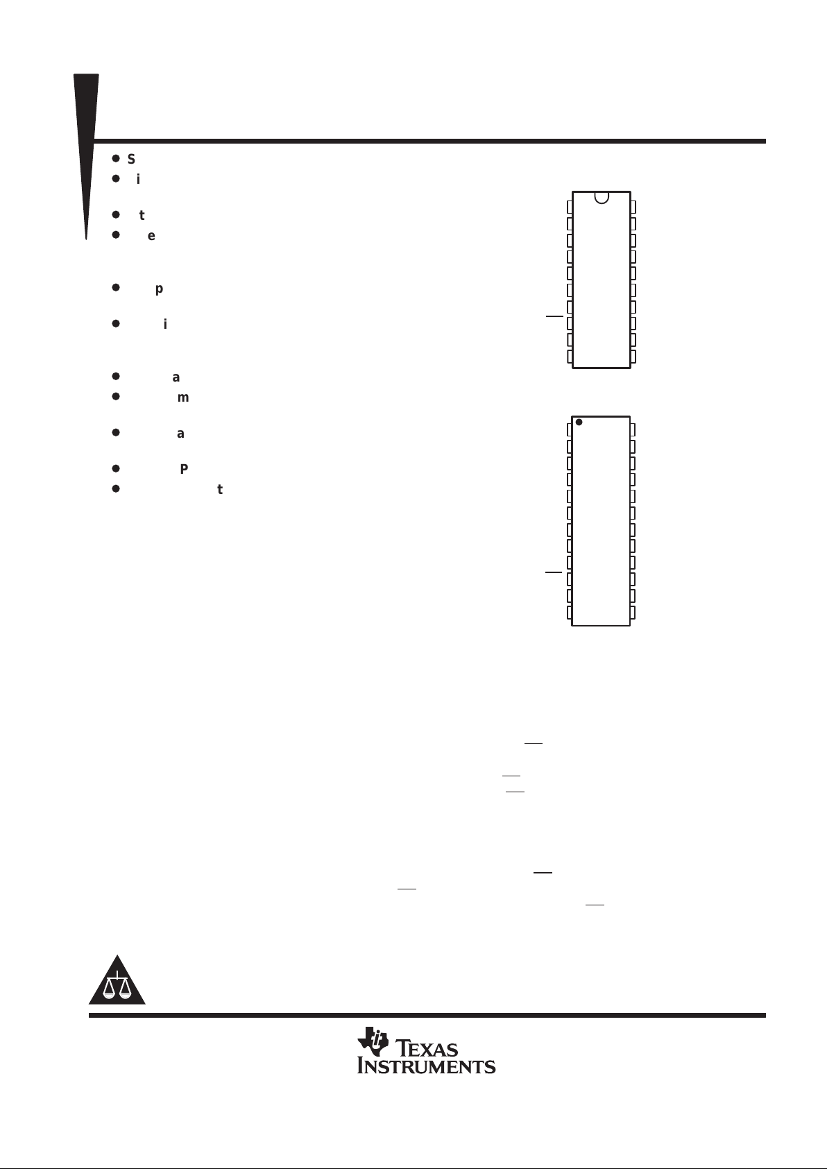
DRAIN5
DRAIN4
SCLK
SDI
GND
GND
SDO
CS
DRAIN3
DRAIN2
V
bat
DRAIN0
NC
NC
GND
GND
NC
NC
DRAIN1
V
CC
NE PACKAGE
(TOP VIEW)
1
2
3
4
5
6
7
8
9
10
11
12
24
23
22
21
20
19
18
17
16
15
14
13
DRAIN5
DRAIN4
SCLK
SDI
GND
GND
GND
GND
SDO
CS
DRAIN3
DRAIN2
V
bat
DRAIN0
NC
NC
GND
GND
GND
GND
NC
NC
DRAIN1
V
CC
DW PACKAGE
(TOP VIEW)
NC – No internal connection
PRODUCTION DATA information is current as of publication date.
Products conform to specifications per the terms of Texas Instruments
standard warranty. Production processing does not necessarily include
testing of all parameters.
TPIC2603
6-CHANNEL SERIAL INTERFACE LOW-SIDE DRIVER
SLIS056A – FEBRUARY 1995 – REVISED MARCH 1996
2
POST OFFICE BOX 655303 • DALLAS, TEXAS 75265
description (continued)
When an over-current or shorted-load fault occurs, the channel transits into a low duty cycle
pulse-width-modulated (PWM) signal as long as the fault is present. More detail on fault detection operation is
presented in the device operation section of this data sheet.
The TPIC2603 provides pulldown resistors on all active-high inputs except SCLK. A pullup resistor is
used on CS
.
The TPIC2603 is characterized for operation over the operating case temperature of –40°C to 125°C.
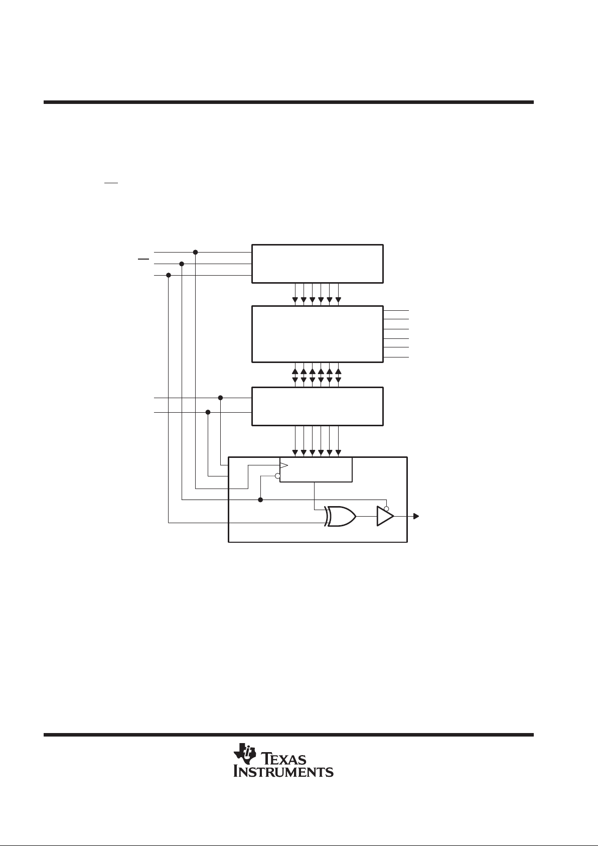
functional block diagram
DRAIN0
DRAIN1
DRAIN2
DRAIN3
DRAIN4
DRAIN5
Fault Register
SDO
Serial Input Control
6-Bit Shift Register
Output Drivers
Fault Sense and Protection
(STB, Current-Limit, Open-Load,
Over-Temperature, Over-Voltage)
SCLK
CS
SDI
V
bat
V
CC
TPIC2603
6-CHANNEL SERIAL INTERFACE LOW-SIDE DRIVER
SLIS056A – FEBRUARY 1995 – REVISED MARCH 1996
3
POST OFFICE BOX 655303 • DALLAS, TEXAS 75265
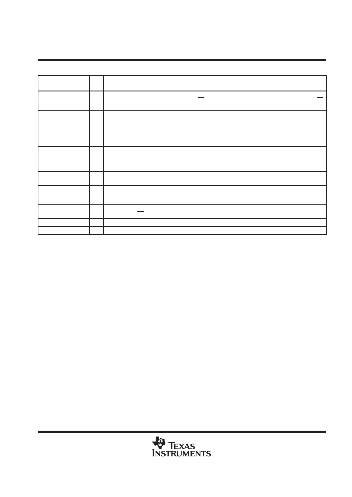
Terminal Functions
TERMINAL
NAME NO.
†
I/O
DESCRIPTION
CS 8 (10) I Chip select. The CS is an active-low input used to select the serial interface of the device. The device accepts
serial input data and transmits fault data when CS
is held low. An internal pullup resistor is provided on the CS
input.
DRAIN0
DRAIN1
DRAIN2
DRAIN3
DRAIN4
DRAIN5
19 (23)
12 (14)
10 (12)
9 (11)
2 (2)
1 (1)
O FET drain outputs. The DRAIN terminals are low-side switches for inductive and resistive loads. Each output
provides an internal drain-gate clamp to snub inductive transients.
GND 5, 6, 15,
16 (5, 6, 7,
8, 17, 18,
19, 20)
O Ground. These terminals provide ground return paths for the device.
SCLK 3 (3) I Serial clock. The SCLK clocks the shift register. Serial data is transferred into the SDI port and serial fault data
is transferred out of the SDO port of the device on the rising edges of SCLK.
SDI 4 (4) I Serial data input. The device receives serial data from the control device using the SDI. Serial input data can
be configured in 8-bit or 16-bit data words. Refer to Figures 2 and 4 for input protocol. An internal pulldown
resistor is provided on the SDI input.
SDO 7 (9) O Serial data output. This 3-state output transfers fault data to the control device after the device has been
selected by the CS
terminal.
V
bat
20 (24) I Battery voltage. The V
bat
terminal monitors the battery voltage to detect over-voltage conditions.
V
CC
11 (13) I Supply voltage. The VCC terminal receives a 5-V supply for internal logic.
†
Terminal numbers listed in parenthesis are for the 24-pin DW package.
absolute maximum ratings over the recommended operating case temperature range (unless
otherwise noted)‡
Logic supply voltage range, VCC (see Note 1) –0.3 V to 7 V. . . . . . . . . . . . . . . . . . . . . . . . . . . . . . . . . . . . . . . . .
Battery supply voltage range, V
bat
–1.5 V to 60 V. . . . . . . . . . . . . . . . . . . . . . . . . . . . . . . . . . . . . . . . . . . . . . . . . .
Logic input voltage range, V
I
–0.3 V to 7 V. . . . . . . . . . . . . . . . . . . . . . . . . . . . . . . . . . . . . . . . . . . . . . . . . . . . . . . .
Power DMOS drain-to-source voltage, V
DS
(see Note 2) 68 V. . . . . . . . . . . . . . . . . . . . . . . . . . . . . . . . . . . . . . .
Continuous drain current, each output, all outputs on, I
D
, T
C
= 25°C 350 mA. . . . . . . . . . . . . . . . . . . . . . . . . . .
Pulsed drain current, single output, I
DM
, T
C
= 25°C (see Note 3) 2.25 A. . . . . . . . . . . . . . . . . . . . . . . . . . . . . . .
Single-pusle avalanche energy, E
AS
(see Figure 11) 100 mJ. . . . . . . . . . . . . . . . . . . . . . . . . . . . . . . . . . . . . . . . .
Continuous total power dissipation See Dissipation Rating Table. . . . . . . . . . . . . . . . . . . . . . . . . . . . . . . . . . . . .
Avalanche current, I
AS
(see Note 4) 1 A. . . . . . . . . . . . . . . . . . . . . . . . . . . . . . . . . . . . . . . . . . . . . . . . . . . . . . . . . .
Operating virtual junction temperature range, T
J
–40°C to 150°C. . . . . . . . . . . . . . . . . . . . . . . . . . . . . . . . . . . .
Storage temperature range, T
stg
–55°C to 150°C. . . . . . . . . . . . . . . . . . . . . . . . . . . . . . . . . . . . . . . . . . . . . . . . . .
Lead temperature 1,6 mm (1/16 inch) from case for 10 seconds 260°C. . . . . . . . . . . . . . . . . . . . . . . . . . . . . . .
‡
Stresses beyond those listed under “absolute maximum ratings” may cause permanent damage to the device. These are stress ratings only, and
functional operation of the device at these or any other conditions beyond those indicated under “recommended operating conditions” is not
implied. Exposure to absolute-maximum-rated conditions for extended periods may affect device reliability.
NOTES: 1. All voltage values are with respect to GND.
2. Each power DMOS source is internally connected to GND.
3. Pulse duration ≤ 100 µs and duty cycle ≤ 2%.
4. DRAIN supply voltage = 13 V, starting junction temperature (TJS) = 25°C, L = 150 mH, IAS = 1 A (see Figure 11).
TPIC2603
6-CHANNEL SERIAL INTERFACE LOW-SIDE DRIVER
SLIS056A – FEBRUARY 1995 – REVISED MARCH 1996
4
POST OFFICE BOX 655303 • DALLAS, TEXAS 75265
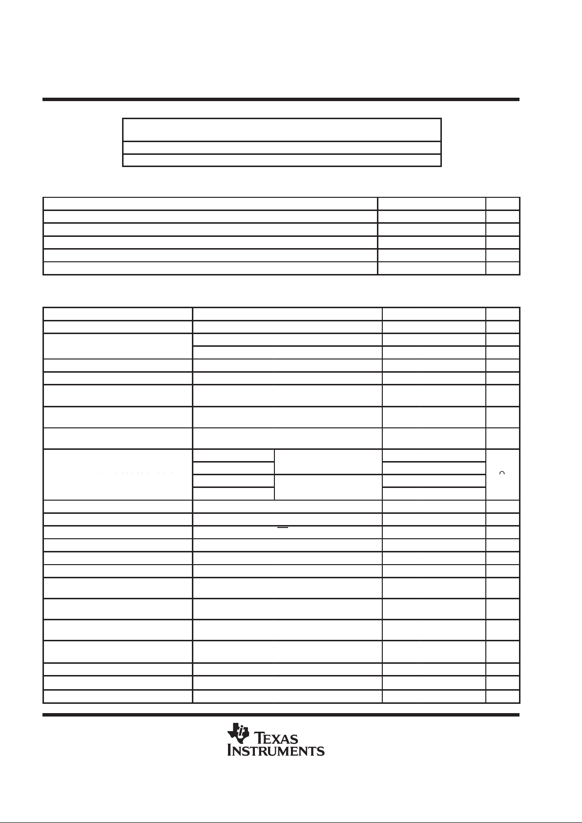
DISSIPATION RATING TABLE
PACKAGE
TC ≤ 25°C
POWER RATING
DERATING FACTOR
ABOVE TC = 25°C
TC = 125°C
POWER RATING
DW 1750 mW 14 mW/°C 350 mW
NE 2500 mW 20 mW/°C 500 mW
recommended operating conditions
MIN NOM MAX UNIT
Logic supply voltage, V
CC
4.5 5 5.5 V
Battery supply voltage, V
bat
5.5 12 25 V
High-level input voltage, V
IH
0.7 V
CC
V
CC
V
Low-level input voltage, V
IL
0 0.3 V
CC
V
Operating case temperature, T
C
–40 125 °C
electrical characteristics, TC = –40°C to 125°C (unless otherwise noted)
PARAMETER TEST CONDITIONS MIN TYP MAX UNIT
V
bat
Battery supply voltage Normal operation 5.5 25 V
pp
VCC = 5 V 5 mA
I
bat
Battery supply current
VCC = 0 50 µA
V
CC
Logic supply voltage 4.5 5.5 V
I
CC
Logic supply current All outputs off, V
bat
= 5.5 V 5 mA
V
(turn-on)
VCC turn-on voltage
(logic operational)
V
bat
= 5.5 V, Check output functionality 4.5 V
V
(ov)
Over-battery voltage
shutdown
Gate disabled 30 38 V
V
hys(ov)
Over-battery voltage reset
hysteresis
0.4 2 V
V
bat
= 13 V
°
0.7 1
Drain-to-source on-state
V
bat
= 5.5 V
I
O
=
0.35 A,T
C
=
25°C
1.7 2.3
r
DS(on)
Drain to source on state
resistance
V
bat
= 13 V
°
1.2 1.7
Ω
V
bat
= 5.5 V
I
O
= 0.35 A,
T
C
=
125°C
2.7 3.8
I
L
On-state current limit 0.8 2 5 A
I
L(sense)
Over-current sense 0.8 1.5 3 A
I
IH
Input pullup current GND < VI < 0.7 VCC, CS input only –5 –10 –50 µA
I
IL
Input pulldown current 0.3 VCC < VI < VCC, All other inputs 2.5 10 25 µA
I
D(off)
Off-state drain current V
load
= V
bat
= 14.5 V 20 40 80 µA
I
O(sleep)
Sleep-state output current V
bat < 0.5 V,
VCC < 0.5 V , Load = 14 V 50 µA
V
OH
High-level serial output
voltage
IO = 1 mA 0.8 V
CC
V
V
OL
Low-level serial output
voltage
IO = 1 mA 0.2 0.4 V
I
OZ
High impedance state
output current
VCC = 5.5 V to 0 V, SDO output –10 1 10 µA
V
(BR)DSX
Drain-to-source breakdown
voltage
dc < 1%, tw = 100 µs, IO = 20 mA 52 58 68 V
T
j(sense)
Thermal flag 150 170 185 °C
T
j(hys)
Thermal flag hysteresis 5 10 15 °C
V
(open)
Open-load detection voltage 0.3V
CC
0.7 V
CC
V
TPIC2603
6-CHANNEL SERIAL INTERFACE LOW-SIDE DRIVER
SLIS056A – FEBRUARY 1995 – REVISED MARCH 1996
5
POST OFFICE BOX 655303 • DALLAS, TEXAS 75265
switching characteristics, VCC = 5 V, T
C
= 25°C
PARAMETER TEST CONDITIONS MIN TYP MAX UNIT
t
w
Clock cycle period pulse duration, SCLK See Figure 1 250 555 ns
t
wH(SCLK)
Pulse duration, SCLK high See Figure 1 100 248 ns
t
wL(SCLK)
Pulse duration, SCLK low See Figure 1 100 248 ns
t
pd1
Propagation delay from falling edge of CS to SDO valid
CS = 0.8 V to SDO low
impedance (see Figure 1)
150 300 ns
t
pd2
Propagation delay from rising edge of CS to SDO 3-state CS = 2 V to SDO 3-state 150 200 ns
t
pd3
Propagation delay from SCLK to SDO valid CS < 0.8 V 80 172 ns
t
r(SDO)
Rise time of SDO C
load
= 200 pF 30 50 ns
t
f(SDO)
Fall time of SDO C
load
= 200 pF 30 50 ns
t
(stb)
Short-to-battery/shorted-load/open-load deglitch time See Figures 5 and 6 25 70 100 µs
t
d(on)
Turn-on delay time, rising edge of CS to drain 0.4 5 10
t
d(off)
Turn-off delay time, rising edge of CS todrain
V
= 14 V
,
0.4 5 15
t
r(drain)
Rise time of drain terminal
V
bat
14
V,
R
load
= 30 Ω
0.4 5 10
µ
s
t
f(drain)
Fall time of drain terminal 0.4 5 10
f
(SCLK)
Serial clock frequency 1.8 4 MHz
t
cyc(ref)
Short-to-battery sense cycle time See Figure 5 1.6 4 6.4 ms
t
w(sense)
Short-to-battery sense pulse duration See Figure 5 25 70 100 µs
t
su1
Setup to/from the fall edge of CS to the rising edge of SCLK See Figure 1 150 200 ns
t
su(SDI)
Setup time, SDI to SCLK See Figure 1 25 55 ns
t
h(SDI)
Hold time, SDI after SCLK See Figure 1 10 55 ns
thermal resistance
PARAMETER TEST CONDITIONS MIN MAX UNIT
R
θJA
Junction-to-ambient thermal resistance All outputs with equal power 50 °C
R
θJC
Junction-to-case thermal resistance All outputs with equal power 10 °C
TPIC2603
6-CHANNEL SERIAL INTERFACE LOW-SIDE DRIVER
SLIS056A – FEBRUARY 1995 – REVISED MARCH 1996
6
POST OFFICE BOX 655303 • DALLAS, TEXAS 75265
PRINCIPLES OF OPERATION
SCLK
t
su1
123X
t
wL(SCLK)
t
wH(SCLK)
t
w
t
su(SDI)
t
h(SDI)
t
pd1
t
pd3
t
pd2
MSB LSB
3-STATE
MSB LSB
3-STATE
CS
SDI
SDO
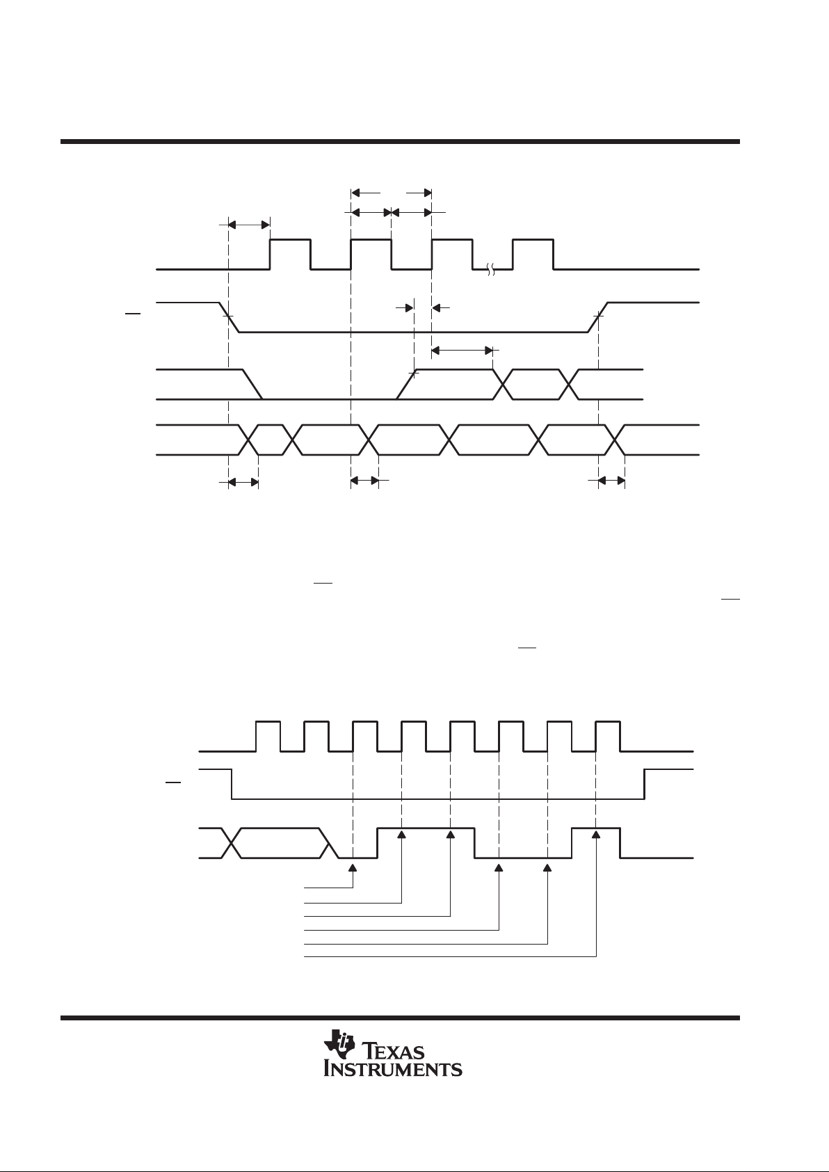
Figure 1. Switching Characteristics
serial interface
Control information is transferred into the TPIC2603 through the serial interface. The serial interface consists
of a serial clock (SCLK), chip select (CS
), serial data input (SDI), and serial data output (SDO). Serial data is
shifted, most significant bit (MSB) first, into the SDI shift register on the rising edge of the first SCLK after CS
has transited from high to low. The controller must shift either eight bits or sixteen bits of data into the device
with the last six bits of input data containing control information for the output drivers. Data bits preceeding the
output control information should be set to 0. A low-to-high transition on CS
latches the contents of the last six
bits of the serial shift register into the output buffer . A low input to SDI turns the corresponding parallel output
OFF and a high input will turn the output ON (see Figure 2).
12345678
DRAIN5 OFF
DRAIN4 ON
DRAIN3 ON
DRAIN2 OFF
DRAIN1 OFF
DRAIN0 ON
0
SCLK
CS
SDI
NEW DATA
Figure 2. Serial Input Control
 Loading...