

TPIC2601
6-CHANNEL COMMON-SOURCE POWER DMOS ARRAY
SLIS048A – NOVEMBER 1996 – REVISED JANUARY 1998
D
Low r
DS(on)
D
High Output Voltage . . . 60 V
D
Pulsed Current . . . 10 A Per Channel
D
Avalanche Energy Capability . . . 105 mJ
D
Input Transient Protection . . . 2000 V
. . . 0.25 Ω Typ
description
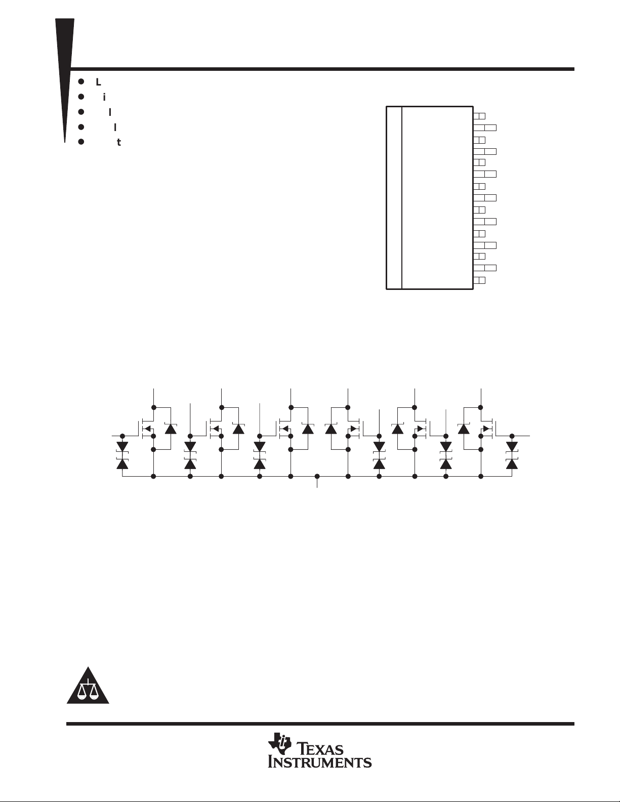
The TPIC2601 is a monolithic power DMOS array
that consists of six electrically isolated N-channel
enhancement-mode DMOS transistors
configured with a common source and open
drains. Each transistor features integrated
high-current zener diodes to prevent gate
damage in the event that an overstress condition
occurs. These zener diodes also provide up to
2000 V of ESD protection when tested using the
human-body model.
†
TI Japan only
KTC or KTD† PACKAGE
(TOP VIEW)
15
14
13
12
11
10
9
8
7
6
5
4
3
2
1
DRAIN6
GATE6
DRAIN5
GATE5
DRAIN4
DRAIN4
GATE4
SOURCE/GND
GATE3
DRAIN3
DRAIN3
GATE2
DRAIN2
GATE1
DRAIN1
The TPIC2601 is offered in a 15-pin PowerFLEX(KTC) package and is characterized for operation over the
case temperature range of –40°C to 125°C.
A 15-pin PowerFLEX(KTD) package is also available for TI Japan
only .
schematic
GATE3
DRAIN3
SOURCE/GND
DRAIN4
8
DRAIN1
1 3 5, 6 10, 11 13 15
Q1 Q2 Q3 Q4 Q5 Q6
GATE1
NOTE A: For correct operation, no drain terminal may be taken below GND.
2
DRAIN2
GATE2
47
DRAIN5
GATE4
912
GATE5
DRAIN6
14
GATE6
Please be aware that an important notice concerning availability, standard warranty, and use in critical applications of
Texas Instruments semiconductor products and disclaimers thereto appears at the end of this data sheet.
PowerFLEX is a trademark of Texas Intruments Incorporated.
PRODUCTION DATA information is current as of publication date.
Products conform to specifications per the terms of Texas Instruments
standard warranty. Production processing does not necessarily include
testing of all parameters.
POST OFFICE BOX 655303 • DALLAS, TEXAS 75265
Copyright 1998, Texas Instruments Incorporated
1
TPIC2601
D
,
DS GS
,
I
Zero-gate-voltage drain current
DS
,
A
r
Static drain-to-source on-state resistance
D
,
Ω
f = 1 MHz
See Figure 11
6-CHANNEL COMMON-SOURCE POWER DMOS ARRAY
SLIS048A – NOVEMBER 1996 – REVISED JANUARY 1998
absolute maximum ratings over operating case temperature range (unless otherwise noted)
†
Drain-to-source voltage, VDS 60 V. . . . . . . . . . . . . . . . . . . . . . . . . . . . . . . . . . . . . . . . . . . . . . . . . . . . . . . . . . . . . .
Gate-to-source voltage, VGS –9 V to 18 V. . . . . . . . . . . . . . . . . . . . . . . . . . . . . . . . . . . . . . . . . . . . . . . . . . . . . . . . .
Continuous drain current, each output, all outputs on, T
= 25°C 2 A. . . . . . . . . . . . . . . . . . . . . . . . . . . . . . . . . .
C
Pulsed drain current, each output, IOmax, TC = 25°C (see Note 1 and Figure 7) 10 A. . . . . . . . . . . . . . . . . . .
Continuous gate-to-source zener diode current, T
Pulsed gate-to-source zener diode current, T
= 25°C ±25 mA. . . . . . . . . . . . . . . . . . . . . . . . . . . . . . . . . . .
C
= 25°C ±250 mA. . . . . . . . . . . . . . . . . . . . . . . . . . . . . . . . . . . . . .
C
Single-pulse avalanche energy, EAS, TC = 25°C (see Figures 4 and 16) 105 mJ. . . . . . . . . . . . . . . . . . . . . . .
Continuous total power dissipation at (or below) T
= 25°C 1.7 W. . . . . . . . . . . . . . . . . . . . . . . . . . . . . . . . . . . . .
A
Power dissipation at (or below) TC = 75°C, all outputs on 18.75 W. . . . . . . . . . . . . . . . . . . . . . . . . . . . . . . . . . . .
Operating virtual junction temperature range, TJ –40°C to 150°C. . . . . . . . . . . . . . . . . . . . . . . . . . . . . . . . . . . . .
Operating case temperature range, T
Storage temperature range, T
stg
–40°C to 125°C. . . . . . . . . . . . . . . . . . . . . . . . . . . . . . . . . . . . . . . . . . . . .
C
–40°C to 125°C. . . . . . . . . . . . . . . . . . . . . . . . . . . . . . . . . . . . . . . . . . . . . . . . . . .
Lead temperature 1,6 mm (1/16 inch) from case for 10 seconds 260°C. . . . . . . . . . . . . . . . . . . . . . . . . . . . . . .
†
Stresses beyond those listed under “absolute maximum ratings” may cause permanent damage to the device. These are stress ratings only, and
functional operation of the device at these or any other conditions beyond those indicated under “recommended operating conditions” is not
implied. Exposure to absolute-maximum-rated conditions for extended periods may affect device reliability.
NOTE 1: Pulse duration = 10 ms, duty cycle = 2%
electrical characteristics, TC = 25°C (unless otherwise noted)
PARAMETER TEST CONDITIONS MIN TYP MAX UNIT
V
(BR)DSX
V
GS(th)
V
GS(th)match
V
(BR)GS
V
(BR)SG
V
DS(on)
V
F(SD)
DSS
I
GSSF
I
GSSR
DS(on)
g
fs
C
iss
C
oss
C
rss
NOTES: 2. Technique should limit TJ – TC to 10°C maximum.
Drain-to-source breakdown voltage ID = 250 µA, VGS = 0 60 V
Gate-to-source threshold voltage
Gate-to-source threshold voltage matching
Gate-to-source breakdown voltage IGS = 250 µA 18 V
Source-to-gate breakdown voltage ISG = 250 µA 9 V
Drain-to-source on-state voltage
Forward on-state voltage, source-to-drain
Forward gate current, drain short circuited to
source
Reverse gate current, drain short circuited to
source
Forward transconductance
Short-circuit input capacitance, common source 180 225
Short-circuit output capacitance, common
source
Short-circuit reverse transfer capacitance,
common source
3. These parameters are measured with voltage-sensing contacts separate from the current-carrying contacts.
I
= 1 mA, V
See Figure 5
ID = 2 A,
See Notes 2 and 3
IS = 2A, VGS = 0,
See Notes 2 and 3 and Figure 12
V
= 48 V,
VGS = 0
VGS = 10 V, VDS = 0 20 200 nA
VSG = 5 V, VDS = 0 10 100 nA
VGS = 10 V,
I
=2 A,
See Notes 2 and 3
and Figures 6 and 7
VDS = 15 V,
See Notes 2 and 3
and Figure 9
VDS = 25 V,
=
,
= V
VGS = 10 V,
TC = 25°C 0.05 1
TC = 125°C 0.5 10
TC = 25°C 0.25 0.3
TC = 125°C 0.4 0.5
ID = 1 A 1.3 1.95 S
VGS = 0,
1.5 2.05 2.2 V
,
0.5 0.6 V
0.85 1 V
110 138
80 100
5 40 mV
µ
pF
2
POST OFFICE BOX 655303 • DALLAS, TEXAS 75265
V
di/dt
100 A/
QRRTotal diod
180nC
DD
,
L
,
en
,
ns
See Figure 3
nH
R
θJC
Junction-to-case thermal resistance
6-CHANNEL COMMON-SOURCE POWER DMOS ARRAY
source-to-drain diode characteristics, TC = 25°C
PARAMETER TEST CONDITIONS MIN TYP MAX UNIT
t
rr(SD)
resistive-load switching characteristics, TC = 25°C
t
d(on)
t
d(off)
t
r
t
f
Q
Q
Q
L
L
R
Reverse-recovery time
Delay time, VGS↑ to VDS↓ turn on 194
Delay time, VGS↓ to VDS↑ turn off
Rise time, V
Fall time, V
Total gate charge
g
Threshold gate-to-source charge
gs(th)
Gate-to-drain charge
gd
D
S
Internal drain inductance 5
Internal source inductance 5
Internal gate resistance 500 Ω
g
e charge
PARAMETER TEST CONDITIONS MIN TYP MAX UNIT
V
= 25 V, R
t
= 10 ns,
DS
DS
dis
VDD = 48 V,
SLIS048A – NOVEMBER 1996 – REVISED JANUARY 1998
IS = 1 A,
= 0,
GS
See Figures 1 and 14
See Figure 2
ID = 1 A, VGS = 10 V,
VDS = 48 V,
=
= 25 Ω,t
= 10 ns,
µs,
TPIC2601
72 ns
430
90
180
5.1 6.4
0.5 0.63
2.75 3.4
nC
thermal resistance
R
Junction-to-ambient thermal resistance All outputs with equal power 72
θJA
PARAMETER TEST CONDITIONS MIN TYP MAX UNIT
All outputs with equal power 4
One output dissipating power 7
°C/W
POST OFFICE BOX 655303 • DALLAS, TEXAS 75265
3
 Loading...