

www.ti.com
1
2
3
4
8
7
6
5
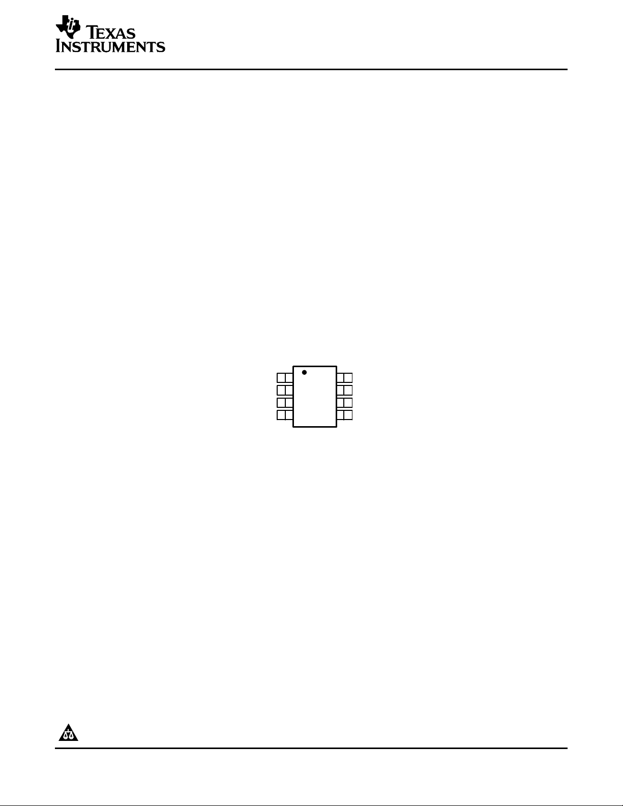
RXD
EN
NWake
TXD
INH
V
SUP
LIN
GND
D PACKAGE
(TOP VIEW)
TPIC1021
LIN Physical Interface
SLIS113C – OCTOBER 2004 – REVISED JULY 2005
FEATURES
• LIN Physical Layer Specification Revision 2.0
• Dominant State Timeout Protection on TXD
Pin
compliant. Conforms to SAEJ2602 • Wake-Up Request on RXD Pin
Recommended Practice for LIN
• Control of External Voltage Regulator (INH
• LIN Bus Speed up to 20 kbps Pin)
• ESD Protection to 12 kV (Human Body Model) • Integrated Pull-Up Resistor and Series Diode
on LIN Pin for LIN Slave Applications
• LIN Pin Handles Voltage from -40 V to +40 V • Low EME (Electromagnetic Emissions), High
• Survives Transient Damage in Automotive
EMI (Electromagnetic Immunity)
Environment (ISO 7637) • Bus Terminal Short-Circuit Protected for
• Operation with Supply from 7 V to 27 V DC
• Two Operation Modes: Normal and Low
Short to Battery or Short to Ground
• Thermally Protected
Power (Sleep) Mode • Ground Disconnection Fail Safe at System
• Low Current Consumption in Low Power
Level
Mode • Ground Shift Operation at System Level
• Wake-Up Available from LIN Bus, Wake-Up • Unpowered Node Does Not Disturb the
Input (External Switch) or Host MCU Network
• Interfaces to MCU with 5 V or 3.3 V I/O Pins
DESCRIPTION
The TPIC1021 is the LIN (Local Interconnect Network) physical interface, which integrates the serial transceiver
with wake up and protection features. The LIN bus is a single wire, bi-directional bus typically used for low-speed
in-vehicle networks using baud rates between 2.4 kbps and 20 kbps.
The LIN bus has two logical values: the dominant state (voltage near ground) represents a logic ‘0’ and the
recessive state (voltage near battery) and represents logic ‘1’.
In the recessive state the LIN bus is pulled high by the TPIC1021’s internal pull-up resistor (30k Ω ) and series
diode, so no external pull-up components are required for slave applications. Master applications require an
external pull-up resistor (1k Ω ) plus a series diode.
The LIN Protocol output data stream on the TXD pin is converted by the TPIC1021 into the LIN bus signal
through a current limited, wave-shaping low-side driver with control as outlined by the LIN Physical Layer
Specification Revision 2.0. The receiver converts the data stream from the LIN bus and outputs the data stream
via the RXD pin.
In Low Power mode, the TPIC1021 requires very low quiescent current even though the wake-up circuits remain
active allowing for remote wake up via the LIN bus or local wake ups via NWake or EN pins.
The TPIC1021 has been designed for operation in the harsh automotive environment. The device can handle LIN
bus voltage swing from +40 V down to ground and survive -40 V. The device also prevents back feed current
through the LIN pin to the supply input in case of a ground shift or supply voltage disconnection. It also features
under-voltage, over temperature, and loss of ground protection. In the event of a fault condition the output is
immediately switched off and remains off until the fault condition is removed.
Please be aware that an important notice concerning availability, standard warranty, and use in critical applications of Texas
Instruments semiconductor products and disclaimers thereto appears at the end of this data sheet.
PRODUCTION DATA information is current as of publication date.
Products conform to specifications per the terms of the Texas
Instruments standard warranty. Production processing does not
necessarily include testing of all parameters.
Copyright © 2004–2005, Texas Instruments Incorporated
www.ti.com
TPIC1021
LIN Physical Interface
SLIS113C – OCTOBER 2004 – REVISED JULY 2005
TERMINAL FUNCTIONS
Terminal Assignments
PIN NAME PIN NO. PIN TYPE DESCRIPTION
RXD 1 O RXD output (open drain) pin interface reporting state of LIN bus voltage
EN 2 I Enable input pin
NWake 3 I High voltage input pin for device wake up
TXD 4 I TXD input pin interface to control state of LIN output
GND 5 I Ground connection
LIN 6 I/O LIN bus pin single wire transmitter and receiver
V
SUP
INH 8 O Inhibit pin controls external voltage regulator with inhibit input
LIN Bus Pin
This I/O pin is the single-wire LIN bus transmitter and receiver.
Transmitter Characteristics
The driver is a low side transistor with internal current limitation and thermal shutdown. There is an internal
30-k Ω pull-up resistor with a serial diode structure to V
slave mode applications. An external pull-up resistor of 1 k Ω plus a series diode to V
device is used for master node applications.
Voltage on the LIN pin can go from -40 V to +40 V DC without any currents other than through the pull-up
resistance. There are no reverse currents from the LIN bus to supply (V
loss of supply (V
The LIN thresholds and ac parameters are compatible LIN Protocol Specification Revision 2.0.
During a thermal shut down condition the driver is disabled.
7 Supply Device supply pin (connected to battery in series with external reverse blocking diode)
so no external pull-up components are required for LIN
sup
), even in the event of a ground shift or
).
sup
sup
must be added when the
sup
Receiver Characteristics
The receiver’s characteristic thresholds are ratio-metric with the device supply pin. Typical thresholds are 50%,
with a hysteresis between 5% and 17.5% of supply.
Transmit Input Pin (TXD)
This pin is the interface to the MCU’s LIN Protocol Controller or SCI/UART used to control the state of the LIN
output. When TXD is low, LIN output is dominant (near ground). When TXD is high, LIN output is recessive (near
battery). TXD input structure is compatible with microcontrollers with 3.3 V and 5.0 V I/O. This pin has an internal
pull-down resistor.
TXD Dominant State Timeout
If the TXD pin is inadvertently driven permanently low by a hardware or software application failure, the LIN bus
is protected by TPIC1021’s Dominant State Timeout Timer. This timer is triggered by a falling edge on the TXD
pin. If the low signal remains on the TXD pin for longer than t
, the transmitter is disabled thus allowing the LIN
DST
bus to return to the recessive state and communication to resume on the bus. The timer is reset by a rising edge
on TXD pin.
Receive Output Pin (RXD)
This pin is the interface to the MCU’s LIN Protocol Controller or SCI/UART, which reports the state of the LIN
bus voltage. LIN recessive (near battery) is represented by a high level on RXD and LIN dominant (near ground)
is represented by a low level on RXD. The RXD output structure is an open-drain output stage. This allows the
TPIC1021 to be used with 3.3 V and 5 V I/O microcontrollers. If the microcontroller’s RXD pin does not have an
integrated pull-up, an external pull-up resistor to the microcontroller I/O supply voltage is required.
2

www.ti.com
TPIC1021
LIN Physical Interface
SLIS113C – OCTOBER 2004 – REVISED JULY 2005
RXD Wake-up Request
When the TPIC1021 has been in low power mode and encounters a wake-up event from the LIN bus or NWake
pin the RXD pin will go LOW while the device enters and remains in Standby Mode (until EN is re-asserted high
and the device enters Normal Mode).
Supply Voltage (V
)
SUP
The TPIC1021 device power supply pin. This pin is connected to the battery through an external reverse battery
blocking diode. The continuous DC operating voltage range for the TPIC1021 is from 7 V to +27 V. The V
SUP
protected to for harsh automotive conditions of up to + 40 V.
The device contains a reset circuit to avoid false bus messages during under-voltage conditions when V
less than V
SUP_UNDER
.
SUP
Ground (GND)
TPIC1021 device ground connection. The TPIC1021 can operate with a ground shift as long as the ground shift
does not reduce V
below the minimum operating voltage. If there is a loss of ground at the ECU level, the
SUP
TPIC1021 will not have a significant current consumption on the LIN pin while in the recessive state (<100 µA
sourced via the LIN pin) and for the dominant state the pull-up resistor should be active.
Enable Input Pin (EN)
The enable input pin controls the operation mode of the TPIC1021 (Normal or Low Power Mode). When enable
is high, the TPIC1021 is in normal mode allowing a transmission path from TXD to LIN and from LIN to RXD.
When the enable input is low, the device is put into low power (sleep) mode and there are no transmission paths.
The device can enter normal operating mode only after being woken up. The enable pin has an internal
pull-down resistor to ensure the device remains in low power mode even if the enable pin floats.
NWake Input Pin (NWake)
The NWake input pin is a high-voltage input used to wake up the TPIC1021 from low power mode. NWake is
usually connected to an external switch in the application. A falling edge on NWake with a low that is asserted
longer than the filter time (t
source to V
.
SUP
) results in a local wake-up. The NWake pin provides an internal pull-up current
NWAKE
is
is
Inhibit Output Pin (INH)
The inhibit output pin is used to control an external voltage regulator that has an inhibit input. When the
TPIC1021 is in normal operating mode, the inhibit high-side switch is enabled and the external voltage regulator
is activated. When TPIC1021 is in low power mode, the inhibit switch is turned off, which disables the voltage
regulator. A wake-up event on for the TPIC1021 will return the INH pin to V
level. The INH pin output current
SUP
is limited to 2 mA. The INH pin can also drive an external transistor connected to an MCU interrupt input.
3
www.ti.com
RXD
TXD
NWake
INH
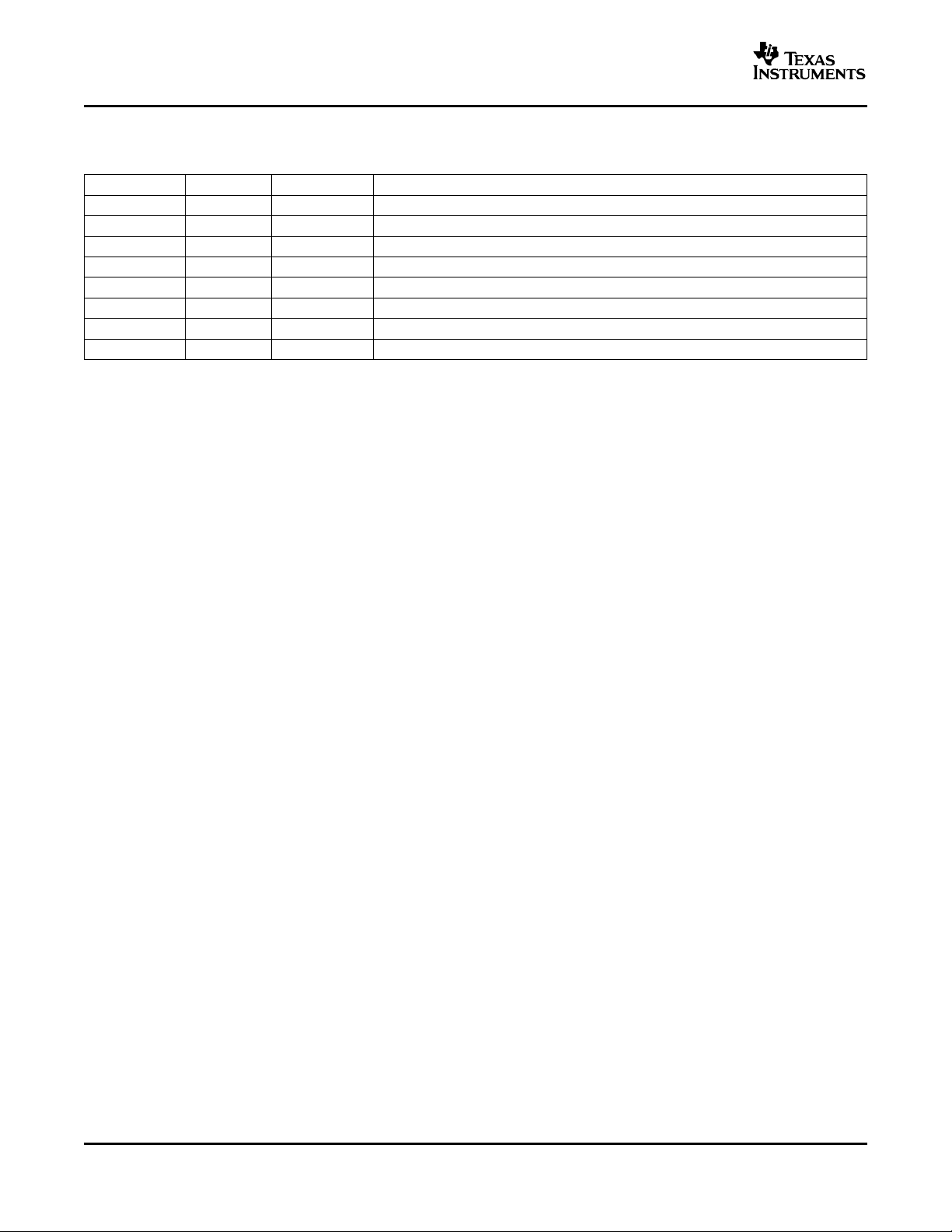
EN
LIN
GND
Driver
Slope Control
Receiver
Filter
Filter
2
1
8
3
4
7
6
5
V
SUP
V
SUP
/2
Wake−Up
and
Vreg Control
Dominant
State
Timeout
Fault
Detection and
Protection
with
Unpowered
System
Standby
Mode
Normal Mode
Low Power
Mode
A
C
A
B
EN = 1
EN = 1
EN = 0
A
LIN Bus Wake−UP
or
NWake Pin Wake−Up
V
SUP
< V
SUP_under
TXD: off
RXD: LOW
IHN: HIGH (high
side switched on)
Term: 30 k
TXD: on
RXD: LIN bus data
IHN: HIGH (high
side switched on)
Term: 30 k
TXD: off
RXD: floating
IHN: high
impedance (high
side switched off)
Term: high
A: V
SUP
< V
SUP_under
B: V
SUP
> V
SUP_unde
, EN = 0
C:V
SUP
> V
SUP_unde
, EN = 1
TPIC1021
LIN Physical Interface
SLIS113C – OCTOBER 2004 – REVISED JULY 2005
Functional Block Diagram
4
OPERATING STATES
Figure 1. Operating States Diagram
www.ti.com
TPIC1021
LIN Physical Interface
SLIS113C – OCTOBER 2004 – REVISED JULY 2005
OPERATING STATES (continued)
Operating Modes
MODE EN RXD LIN BUS INH TRANSMITTER COMMENTS
Low Power 0 Floating High impedance High impedance Off
Standby 0 Low 30 k Ω (typical) High Off Wake-up event detected,
Normal 1 LIN bus data 30 k Ω (typical) High On
Normal Mode
This is the normal operational mode where the receiver and driver are active. The receiver detects the data
stream on the LIN bus and outputs it on the RXD pin for the LIN controller where recessive on the LIN bus is a
digital high and dominate on the LIN bus is digital low. The driver will transmit input data on the TXD pin to the
LIN bus.
Low Power Mode
The power saving mode for the TPIC1021 and the default state after power-up (assuming EN=0). Even with the
extremely low current consumption in this mode, the TPIC1021 can still wake-up from LIN bus activity, a falling
edge on the NWake pin or if EN is set high. The LIN bus and NWake pins are filtered to prevent false wake-up
events. The wake-up events must be active for their respective time periods: t
The low power mode is entered by setting the EN pin low.
While the device is in low power mode the following conditions exist:
• The LIN bus driver is disabled and the internal LIN bus termination is switched off (to minimize power loss if
LIN is short-circuited to ground).
• The normal receiver is disabled.
• The INH pin is high impedance.
• EN input, NWake input and the LIN wake-up receiver are active.
TERMINATION
waiting on MCU to set EN
, t
LINBUS
.
NWake
Wake-Up Events
There are three ways to wake-up the TPIC1021 from Low Power Mode.
• Remote wake-up via recessive (high) to dominant (low) state transition on LIN Bus where dominant bus state
of 50% threshold is detected. The dominant state must be held for t
filter time (to eliminate false wake
LINBUS
ups from disturbances on the LIN Bus).
• Local wake-up via falling edge on NWake pin which is held low for filter time t
(to eliminate false wake
NWake
ups from disturbances on NWake).
• Local wake-up via EN being set high
Standby Mode
This mode is entered whenever a wake-up event occurs via the LIN bus or NWake pin while the TPIC1021 is in
low power mode. The LIN bus slave termination circuit and the INH pin are turned on when standby mode is
entered. The application system will power up once the INH pin is turn assuming it is using a voltage regulator
connected via INH pin. Standby Mode is signaled via a low level on RXD pin.
When EN pin is set high while the TPIC1021 is in Standby Mode the device returns to Normal Mode and the
normal transmission paths from TXD to LIN bus and LIN bus to RXD are turned on.
5

www.ti.com
LIN
INH
EN
RXD
MODE
t
LINBUS
V
SUP
High Impedance
Floating
Low Power
System Wake−Up Time (Vreg + MCU)
Standby Normal
NWake
INH
EN
RXD
MODE
t
NWake
V
SUP
High Impedance
Floating
Low Power
System Wake−Up Time (Vreg + MCU)
Standby Normal
Falling Edge on NWake
TPIC1021
LIN Physical Interface
SLIS113C – OCTOBER 2004 – REVISED JULY 2005
Figure 2. Wake-Up Via LIN Bus Timing Diagram
6
Figure 3. Wake-Up Via NWake Timing Diagram

www.ti.com
LIN Physical Interface
SLIS113C – OCTOBER 2004 – REVISED JULY 2005
ABSOLUTE MAXIMUM RATINGS
over operating free-air temperature range (unless otherwise noted)
(2)
V
SUP
T
A
T
J
T
stg
R
θ JA
(1) Stresses beyond those listed under “absolute maximum ratings” may cause permanent damage to the device. These are stress ratings
only and functional operation of the device at these or any other conditions beyond those indicated under “recommended operating
conditions” is not implied. Exposure to absolute-maximum-rated conditions for extended periods may affect device reliability.
(2) All voltage values are with respect to GND.
(3) The human body model is a 100-pF capacitor discharged through a 1.5-k Ω resistor into each pin.
(4) The machine model is a 200-pF capacitor through a 10- Ω resistor and a 0.75-µH coil.
Supply line supply voltage (continuous) 0 to 27 V
Supply line supply voltage (transient) 0 to 40 V
NWake DC and transient input voltage (through 33-k Ω serial resistor) -1 to 40 V
Logic pin input voltage (RXD, TXD, EN) -0.3 to 5.5 V
LIN DC input voltage -40 to 40 V
Electrostatic discharge: Human Body Model: LIN pin
Electrostatic discharge: Human Body Model: NWake pin
Electrostatic discharge: Human Body Model: All other pins
Electrostatic discharge: Machine Model: LIN and NWake pins
Electrostatic discharge: Machine Model: All other pins
Operational free-air temperature -40 to 125 °C
Junction temperature -40 to 150 °C
Storage temperature -40 to 165 °C
Thermal resistance, junction-to-ambient 145 °C/W
Thermal shutdown 200 °C
Thermal shutdown hysteresis 25 °C
(1)
PARAMETER RATING UNIT
(3)
(3)
(3)
(4)
(4)
-12 to 12 kV
-9 to 9 kV
-3 to 3 kV
-400 to 400 V
-200 to 200 V
TPIC1021
7

www.ti.com
TPIC1021
LIN Physical Interface
SLIS113C – OCTOBER 2004 – REVISED JULY 2005
ELECTRICAL CHARACTERISTICS
V
= 7 V to 27 V, TA= -40°C to 125°C (unless otherwise noted)
SUP
PARAMETER TEST CONDITIONS MIN TYP
SUPPLY
Operational supply voltage
Nominal supply line voltage
V
undervoltage threshold
SUP
I
CC
Supply Current Normal Mode, EN = 1, Bus domi- 1.2 2.5 mA
RXD OUTPUT PIN
V
O
I
OL
I
IKG
Output voltage -0.3 5.5 V
Low-level output current, open drain LIN = 0 V, RXD = 0.4 V 3.5 mA
Leakage current, high-level LIN = V
TXD INPUT PIN
V
IL
V
IH
V
IT
Low-level input voltage
High-level input voltage
Input threshold hysteresis voltage
Pull-down resistor 125 350 800 k Ω
I
IL
Low-level input current TXD = 0 -5 0 5 µA
LIN PIN (Referenced to V
V
OH
V
OL
High-level output voltage
Low-level output voltage
Pull-up resistor to V
I
L
I
IKG
V
IL
V
IH
V
IT
V
hys
V
IL
Limiting current TXD = Low 50 150 250 mA
Leakage current LIN = V
Low-level input voltage
High-level input voltage
Input threshold voltage
Hysteresis voltage
Low-level input voltage for 0 0.4 × V
wake-up
EN PIN
V
IL
V
IH
V
hys
Low-level input voltage
High-level input voltage
Hysteresis voltage
)
SUP
(2)
(2)
(2)
(2)
(2)
(2)
(2)
(2)
SUP
(2)
(2)
(2)
(2)
(2)
(2)
(2)
(1)
7 14 27 V
7 14 18 V
4.5 V
nant (total bus load > 500 Ω )
Standby Mode, EN = 0, Bus domi- 1 2.1 mA
nant (total bus load > 500 Ω )
(3)
(3)
Normal Mode, EN = 1, Bus recess- 300 500 µA
ive
Standby Mode, EN = 0, Bus recess- 300 500 µA
ive
Low Power Mode, EN = 0, V
14 V, NWake = V
SUP
, LIN = V
< 20 50 µA
SUP
SUP
Low Power Mode, EN = 0, 14 V < 50 100 µA
V
< 27 V, NWake = V
SUP
V
SUP
SUP
, RXD = 5 V -5 0 5 µA
, LIN =
SUP
-0.3 0.8 V
2 5.5 V
(2)
LIN recessive, TXD = High, IO= 0 V
mA
30 500 mV
-1V V
SUP
LIN dominant, TXD = Low, IO= 40 0 0.2 × V
mA
20 30 60 k Ω
SUP
LIN dominant 0 × V
LIN recessive 0.6 × V
0.05 × V
-5 0 5 µA
SUP
SUP
0.4 × V
0.5 × V
SUP
SUP
SUP
0.4 × V
0.6 × V
0.175 × V
-0.3 0.8 V
2 5.5 V
30 500 mV
MAX UNIT
V
SUP
SUP
SUP
SUP
SUP
SUP
V
V
V
V
V
V
(1) Typical values are give for V
(2) All voltages are defined with respect to ground; positive currents flow into the TPIC1021 device.
= 14 V at 25°C.
SUP
(3) In the dominant state the supply current increases as the supply voltage increases due to the integrated LIN slave termination
resistance. At higher voltages the majority of supply current is through the termination resistance. The minimum resistance of the LIN
slave termination is 20 k Ω so the maximum supply current attributed to the termination is: I
(V
LIN_Dominant
+0.7V) / 20 k Ω .
SUP (dom) max termination
≈ (V
8
–
SUP

www.ti.com
ELECTRICAL CHARACTERISTICS (continued)
V
= 7 V to 27 V, TA= -40°C to 125°C (unless otherwise noted)
SUP
PARAMETER TEST CONDITIONS MIN TYP
Pull-down resistor 125 350 800 k Ω
I
IL
INH PIN
V
o
I
O
R
on
I
IKG
NWake PIN
V
IL
V
IH
I
IKG
THERMAL SHUTDOWN
AC CHARACTERISTICS
D1 Duty cycle 1
D2 Duty cycle 2
D3 Duty cycle 3
D4 Duty cycle 4
t
rx_pdr
t
rx_pdf
t
rx_sym
t
NWake
t
LINBUS
t
DST
Low-level input current EN = 0 V -5 0 5 µA
DC output voltage Transient voltage -0.3 V
Ouptut current -50 2 mA
On state resistance Between V
Leakage current Low Power mode, 0 < INH < V
Low-level input voltage
High-level input voltage
(4)
(4)
Pull-up current NWake = 0 V -40 -10 -4 µA
Leakage current V
Shutdown junction thermal tempera- 185 °C
ture
(5) (6)
(5) (6)
(5) (6)
(5) (6)
Receiver rising propagation delay RL= 2.4 k Ω , CL= 20 pF, See 6 µs
time Figure 4
Receiver falling propagation delay RL= 2.4 k Ω , CL= 20 pF, See 6 µs
time Figure 4
Symmetry of receiver propagation wrt falling edge, See Figure 4 -2 2 µs
delay time (rising edge)
NWake filter time for local wake-up See Figure 4 25 50 100 µs
LIN wake-up filter time (dominant See Figure 4 25 50 100 µs
time for wake-up via LIN bus)
Dominant state timeout
(7)
TPIC1021
LIN Physical Interface
SLIS113C – OCTOBER 2004 – REVISED JULY 2005
(1)
and INH, INH = 2 mA 25 40 100 Ω
drive, Normal or Standby Mode
SUP
SUP
-5 0 5 µA
-0.3 V
V
-1 V
SUP
= NWake -5 0 5 µA
SUP
TH
REC(max)
TH
DOM(max)
7.0 V to 18 V, t
See Figure 4
TH
REC(max)
TH
DOM(max)
7.6 V to 18 V, t
See Figure 4
TH
REC(max)
TH
DOM(max)
7.0 V to 18 V, t
kbps), See Figure 4
TH
REC(max)
TH
DOM(max)
7.6 V to 18 V, t
kbps), See Figure 4
= 0.744×V
= 0.581×V
BIT
= 0.284×V
= 0.422×V
BIT
= 0.778×V
= 0.616×V
BIT
= 0.251×V
= 0.389×V
BIT
, 0.396
SUP
, V
= 50 µs (20 kbps),
SUP
= 50 µs (20 kbps),
SUP
= 96 µs (10.4
SUP
= 96 µs (10.4
SUP
SUP
SUP
SUP
=
SUP
, 0.581
, V
=
SUP
, 0.417
, V
=
SUP
, 0.590
, V
=
SUP
See Figure 4 6 9 14 ms
SUP
SUP
SUP
MAX UNIT
+0.3 V
-3.3 V
+0.3 V
(4) All voltages are defined with respect to ground; positive currents flow into the TPIC1021 device.
(5) Duty cycle = t
(6) Duty Cycles: LIN Driver bus load conditions (CLINBUS, RLINBUS): Load1 = 1 nF, 1 k Ω ; Load2 = 6.8 nF, 660 Ω ; Load3 = 10 nF, 500 Ω .
BUS_rec(min)
/ (2×t
)
BIT
Duty Cycles 3 and 4 are defined for 10.4 kbps operation. The TPIC1021 also meets these lower speed requirements, while it is capable
of of the higher speed 20.0 kbps operation as specified by Duty Cycles 1 and 2. SAEJ2602 derives propagation delay equations from
the LIN 2.0 duty cycle definitions, for details please refer to the SAEJ2602 specification.
(7) Dominant state timeout will limit the minimum data rate to 2.4 kbps.
9

www.ti.com
LIN Bus Signal
TH
Rec(max)
TH
Dom(max)
TH
Rec(min)
TH
Dom(min)
Thresholds of
receiving node 1
Thresholds of
receiving node 2
V
SUP
(Transceiver supply
of transmitting node)
TXD (Input)
DOMINANT
RECESSIVE
t
Bit
t
Bit
t
Bit
t
Bus_dom(max)
t
Bus_rec(min)
t
Bus_dom(min)
t
Bus_rec(max)
RXD
(Output of receiving node 1)
t
rx_pdf(1)
t
rx_pdr(1)
t
rx_pdr(2)
t
rx_pdf(2)
RXD
(Output of receiving node 2)
TPIC1021
LIN Physical Interface
SLIS113C – OCTOBER 2004 – REVISED JULY 2005
TIMING DIAGRAMS
10
Figure 4. Definition of Bus Timing Parameters

www.ti.com
V
bat
V
BAT
V
SUP
TPIC7xxxx
V
SUP
V
DD
V
DD
V
DD
V
SUP
INH
NWake
TPIC1021
MCU
MASTER
NODE
TMS430
TMS470
LIN
Controller
or
SCI/UART
1
EN
RXD
TXD
MCU w/o
pull−up
2
V
DD
I/O
GND
2
8 3 7
1
4 5
6
Master Node
Pull−Up
3
1 kΩ
LIN
220 pF
V
SUP
TPIC7xxxx
V
SUP
V
DD
V
DD
V
SUP
INH
NWake
TPIC1021
MCU
TMS430
TMS470
LIN
Controller
or
SCI/UART
1
EN
TXD
MCU w/o
pull−up
2
V
DD
I/O
GND
2
8 3 7
1
4 5
6
LIN
220 pF
RXD
SLAVE
NODE
LIN Bus
TPIC1021
LIN Physical Interface
SLIS113C – OCTOBER 2004 – REVISED JULY 2005
APPLICATION INFORMATION
Figure 5.
11
(1) RXD on MCU or LIN Slave has internal pull-up, no external pull-up resistor is needed.
(2) RXD on MCU or LIN Slave without internal pull-up, requires external pull-up resistor.
(3) Master Node applications require an external 1-k Ω pull-up resistor and serial diode.

PACKAGE OPTION ADDENDUM
www.ti.com
20-Oct-2007
PACKAGING INFORMATION
Orderable Device Status
(1)
Package
Type
Package
Drawing
Pins Package
Qty
Eco Plan
TPIC1021D ACTIVE SOIC D 8 75 TBD CU NIPDAU Level-1-235C-UNLIM
TPIC1021DR ACTIVE SOIC D 8 2500 TBD CU NIPDAU Level-1-235C-UNLIM
(1)
The marketing status values are defined as follows:
ACTIVE: Product device recommended for new designs.
LIFEBUY: TI has announced that the device will be discontinued, and a lifetime-buy period is in effect.
NRND: Not recommended for new designs. Device is in production to support existing customers, but TI does not recommend using this part in
a new design.
PREVIEW: Device has been announced but is not in production. Samples may or may not be available.
OBSOLETE: TI has discontinued the production of the device.
(2)
Eco Plan - The planned eco-friendly classification: Pb-Free (RoHS), Pb-Free (RoHS Exempt), or Green (RoHS & no Sb/Br) - please check
http://www.ti.com/productcontent for the latest availability information and additional product content details.
TBD: The Pb-Free/Green conversion plan has not been defined.
Pb-Free (RoHS): TI's terms "Lead-Free" or "Pb-Free" mean semiconductor products that are compatible with the current RoHS requirements
for all 6 substances, including the requirement that lead not exceed 0.1% by weight in homogeneous materials. Where designed to be soldered
at high temperatures, TI Pb-Free products are suitable for use in specified lead-free processes.
Pb-Free (RoHS Exempt): This component has a RoHS exemption for either 1) lead-based flip-chip solder bumps used between the die and
package, or 2) lead-based die adhesive used between the die and leadframe. The component is otherwise considered Pb-Free (RoHS
compatible) as defined above.
Green (RoHS & no Sb/Br): TI defines "Green" to mean Pb-Free (RoHS compatible), and free of Bromine (Br) and Antimony (Sb) based flame
retardants (Br or Sb do not exceed 0.1% by weight in homogeneous material)
(2)
Lead/Ball Finish MSL Peak Temp
(3)
(3)
MSL, Peak Temp. -- The Moisture Sensitivity Level rating according to the JEDEC industry standard classifications, and peak solder
temperature.
Important Information and Disclaimer:The information provided on this page represents TI's knowledge and belief as of the date that it is
provided. TI bases its knowledge and belief on information provided by third parties, and makes no representation or warranty as to the
accuracy of such information. Efforts are underway to better integrate information from third parties. TI has taken and continues to take
reasonable steps to provide representative and accurate information but may not have conducted destructive testing or chemical analysis on
incoming materials and chemicals. TI and TI suppliers consider certain information to be proprietary, and thus CAS numbers and other limited
information may not be available for release.
In no event shall TI's liability arising out of such information exceed the total purchase price of the TI part(s) at issue in this document sold by TI
to Customer on an annual basis.
Addendum-Page 1

IMPORTANT NOTICE
Texas Instruments Incorporated and its subsidiaries (TI) reserve the right to make corrections, modifications, enhancements,
improvements, and other changes to its products and services at any time and to discontinue any product or service without notice.
Customers should obtain the latest relevant information before placing orders and should verify that such information is current and
complete. All products are sold subject to TI’s terms and conditions of sale supplied at the time of order acknowledgment.
TI warrants performance of its hardware products to the specifications applicable at the time of sale in accordance with TI’s
standard warranty. Testing and other quality control techniques are used to the extent TI deems necessary to support this
warranty. Except where mandated by government requirements, testing of all parameters of each product is not necessarily
performed.
TI assumes no liability for applications assistance or customer product design. Customers are responsible for their products and
applications using TI components. To minimize the risks associated with customer products and applications, customers should
provide adequate design and operating safeguards.
TI does not warrant or represent that any license, either express or implied, is granted under any TI patent right, copyright, mask
work right, or other TI intellectual property right relating to any combination, machine, or process in which TI products or services
are used. Information published by TI regarding third-party products or services does not constitute a license from TI to use such
products or services or a warranty or endorsement thereof. Use of such information may require a license from a third party under
the patents or other intellectual property of the third party, or a license from TI under the patents or other intellectual property of TI.
Reproduction of TI information in TI data books or data sheets is permissible only if reproduction is without alteration and is
accompanied by all associated warranties, conditions, limitations, and notices. Reproduction of this information with alteration is an
unfair and deceptive business practice. TI is not responsible or liable for such altered documentation. Information of third parties
may be subject to additional restrictions.
Resale of TI products or services with statements different from or beyond the parameters stated by TI for that product or service
voids all express and any implied warranties for the associated TI product or service and is an unfair and deceptive business
practice. TI is not responsible or liable for any such statements.
TI products are not authorized for use in safety-critical applications (such as life support) where a failure of the TI product would
reasonably be expected to cause severe personal injury or death, unless officers of the parties have executed an agreement
specifically governing such use. Buyers represent that they have all necessary expertise in the safety and regulatory ramifications
of their applications, and acknowledge and agree that they are solely responsible for all legal, regulatory and safety-related
requirements concerning their products and any use of TI products in such safety-critical applications, notwithstanding any
applications-related information or support that may be provided by TI. Further, Buyers must fully indemnify TI and its
representatives against any damages arising out of the use of TI products in such safety-critical applications.
TI products are neither designed nor intended for use in military/aerospace applications or environments unless the TI products are
specifically designated by TI as military-grade or "enhanced plastic." Only products designated by TI as military-grade meet military
specifications. Buyers acknowledge and agree that any such use of TI products which TI has not designated as military-grade is
solely at the Buyer's risk, and that they are solely responsible for compliance with all legal and regulatory requirements in
connection with such use.
TI products are neither designed nor intended for use in automotive applications or environments unless the specific TI products
are designated by TI as compliant with ISO/TS 16949 requirements. Buyers acknowledge and agree that, if they use any
non-designated products in automotive applications, TI will not be responsible for any failure to meet such requirements.
Following are URLs where you can obtain information on other Texas Instruments products and application solutions:
Products Applications
Amplifiers amplifier.ti.com Audio www.ti.com/audio
Data Converters dataconverter.ti.com Automotive www.ti.com/automotive
DSP dsp.ti.com Broadband www.ti.com/broadband
Interface interface.ti.com Digital Control www.ti.com/digitalcontrol
Logic logic.ti.com Military www.ti.com/military
Power Mgmt power.ti.com Optical Networking www.ti.com/opticalnetwork
Microcontrollers microcontroller.ti.com Security www.ti.com/security
RFID www.ti-rfid.com Telephony www.ti.com/telephony
Low Power www.ti.com/lpw Video & Imaging www.ti.com/video
Wireless
Wireless www.ti.com/wireless
Mailing Address: Texas Instruments, Post Office Box 655303, Dallas, Texas 75265
Copyright © 2007, Texas Instruments Incorporated
 Loading...