

TPIC0107B
PWM CONTROL INTELLIGENT H-BRIDGE
SLIS067 – NOVEMBER 1998
1
POST OFFICE BOX 655303 • DALLAS, TEXAS 75265
D
Dedicated PWM Input Port
D
Optimized for Reversible Operation of
Motors
D
Two Input Control Lines for Reduced
Microcontroller Overhead
D
Internal Current Shutdown of 5 A
D
40 V Load Dump Rating
D
Integrated Fault Protection and Diagnostics
D
CMOS Compatible Schmitt Trigger Inputs
for High Noise Immunity
description
The TPIC0107B is a PWM control intelligent H-bridge designed specifically for dc motor applications. The
device provides forward, reverse, and brake modes of operation. A logic supply voltage of 5 V is internally
derived from V
CC
.
The TPIC0107B has an extremely low r
DS(on)
, 280 mΩ typical, to minimize system power dissipation. The
direction control (DIR) and PWM control (PWM) inputs greatly simplify the microcontroller overhead
requirement. The PWM input can be driven from a dedicated PWM port while the DIR input is driven as a simple
low speed toggle.
The TPIC0107B provides protection against over-voltage, over-current, over-temperature, and cross
conduction faults. Fault diagnostics can be obtained by monitoring the ST ATUS1 and STATUS2 terminals and
the two input control lines. STATUS1 is an open-drain output suitable for wired-or connection. STATUS2 is a
push-pull output that provides a latched status output. Under-voltage protection ensures that the outputs, OUT1
and OUT2, will be disabled when V
CC
is less than the under-voltage detection voltage V
(UVCC)
.
The TPIC0107B is designed using TI’s LinBiCMOS process. LinBiCMOS allows the integration of low power
CMOS structures, precision bipolar cells, and low impedance DMOS transistors.
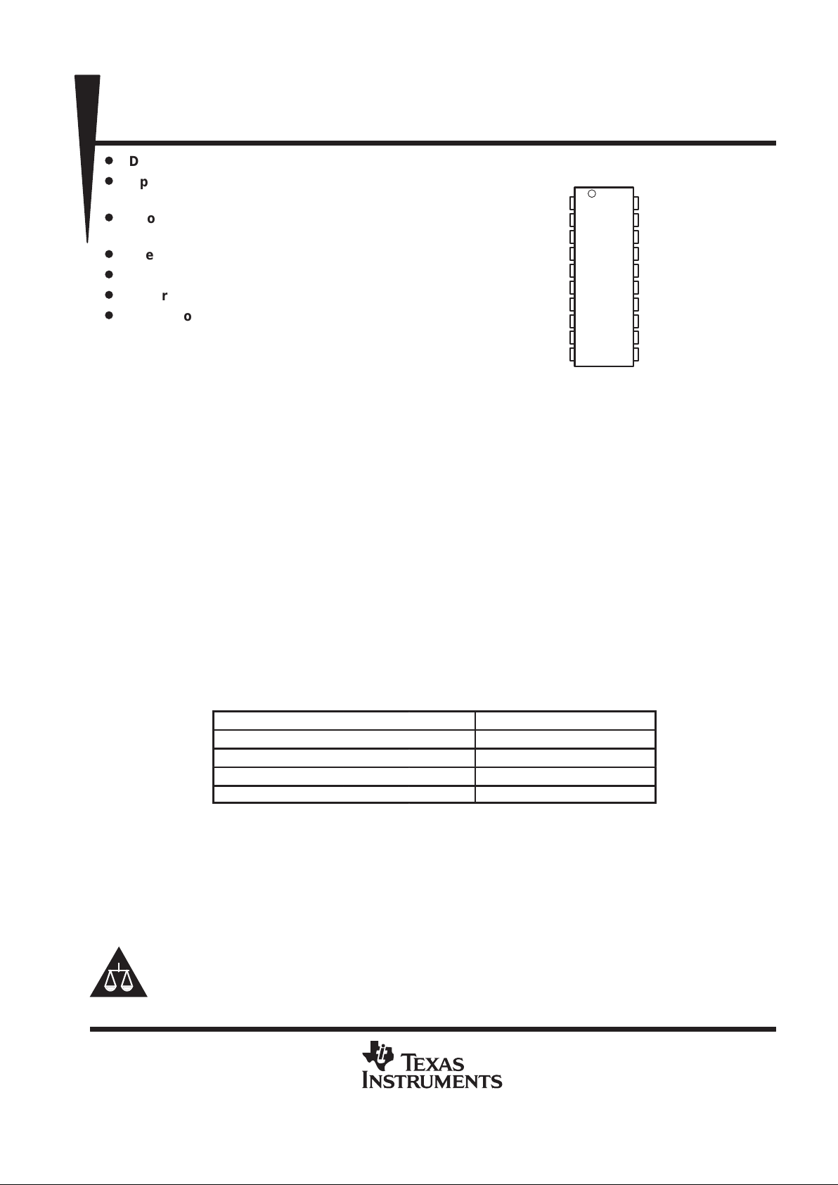
The TPIC0107B is offered in a 20-pin thermally enhanced small-outline package (DWP) and is characterized
for operation over the operating case temperature of –40°C to 125°C.
FUNCTION TABLE
DIR
PWM OUT1 OUT2 MODE
0 0 HS HS Brake, both HSDs turned on hard
0 1 HS LS Motor turns counter clockwise
1 0 HS HS Brake, both HSDs turned on hard
1 1 LS HS Motor turns clockwise
Please be aware that an important notice concerning availability, standard warranty, and use in critical applications of
Texas Instruments semiconductor products and disclaimers thereto appears at the end of this data sheet.
LinBiCMOS is a trademark of Texas Instruments Incorporated.
Copyright 1998, Texas Instruments Incorporated
1
2
3
4
5
6
7
8
9
10
20
19
18
17
16
15
14
13
12
11
GNDS
V
CC
DIR
V
CC
OUT1
OUT1
GND
PWM
GND
GNDS
GNDS
V
CC
STATUS2
V
CC
OUT2
OUT2
GND
STATUS1
GND
GNDS
DWP PACKAGE
(TOP VIEW)
PRODUCTION DATA information is current as of publication date.
Products conform to specifications per the terms of Texas Instruments
standard warranty. Production processing does not necessarily include
testing of all parameters.
TPIC0107B
PWM CONTROL INTELLIGENT H-BRIDGE
SLIS067 – NOVEMBER 1998
2
POST OFFICE BOX 655303 • DALLAS, TEXAS 75265
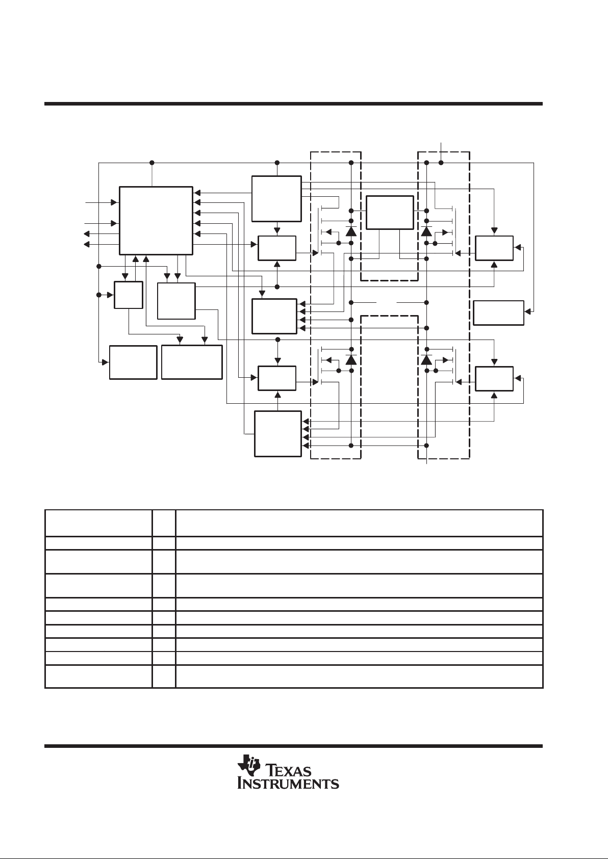
block diagram
Logic
5 V
Reg.
Charge
Pump
(2 MHz)
Over-
Current
Protection
HSD
DMOS
Driver
OpenCircuit
Detect
Under-
Voltage
Detection
Over-
Temperature
Detection
DMOS
Driver
Over-
Current
Protection
LSD
Over-
Voltage
Detection
DMOS
Driver
DMOS
Driver
OUT2 OUT1
DMOS
Driver
Load-Dump
Protection
GND
PWM
DIR
STATUS1
STATUS2
V
CC
Terminal Functions
TERMINAL
NAME NO.
I/O
DESCRIPTION
DIR 3 I Direction control input
GND 7, 9,
12, 14
I Power ground
GNDS 1, 10,
11, 20
I Substrate ground
OUT1 5, 6 O Half-H output. DMOS output
OUT2 15, 16 O Half-H output. DMOS output
PWM 8 I PWM control input
STATUS1 13 O Status output
STATUS2 18 O Latched status output
V
CC
2, 4,
17, 19
I Supply voltage
NOTE: It is mandatory that all four ground terminals plus at least one substrate terminal are connected to the system ground. Use all VCC and
OUT terminals.
TPIC0107B
PWM CONTROL INTELLIGENT H-BRIDGE
SLIS067 – NOVEMBER 1998
3
POST OFFICE BOX 655303 • DALLAS, TEXAS 75265
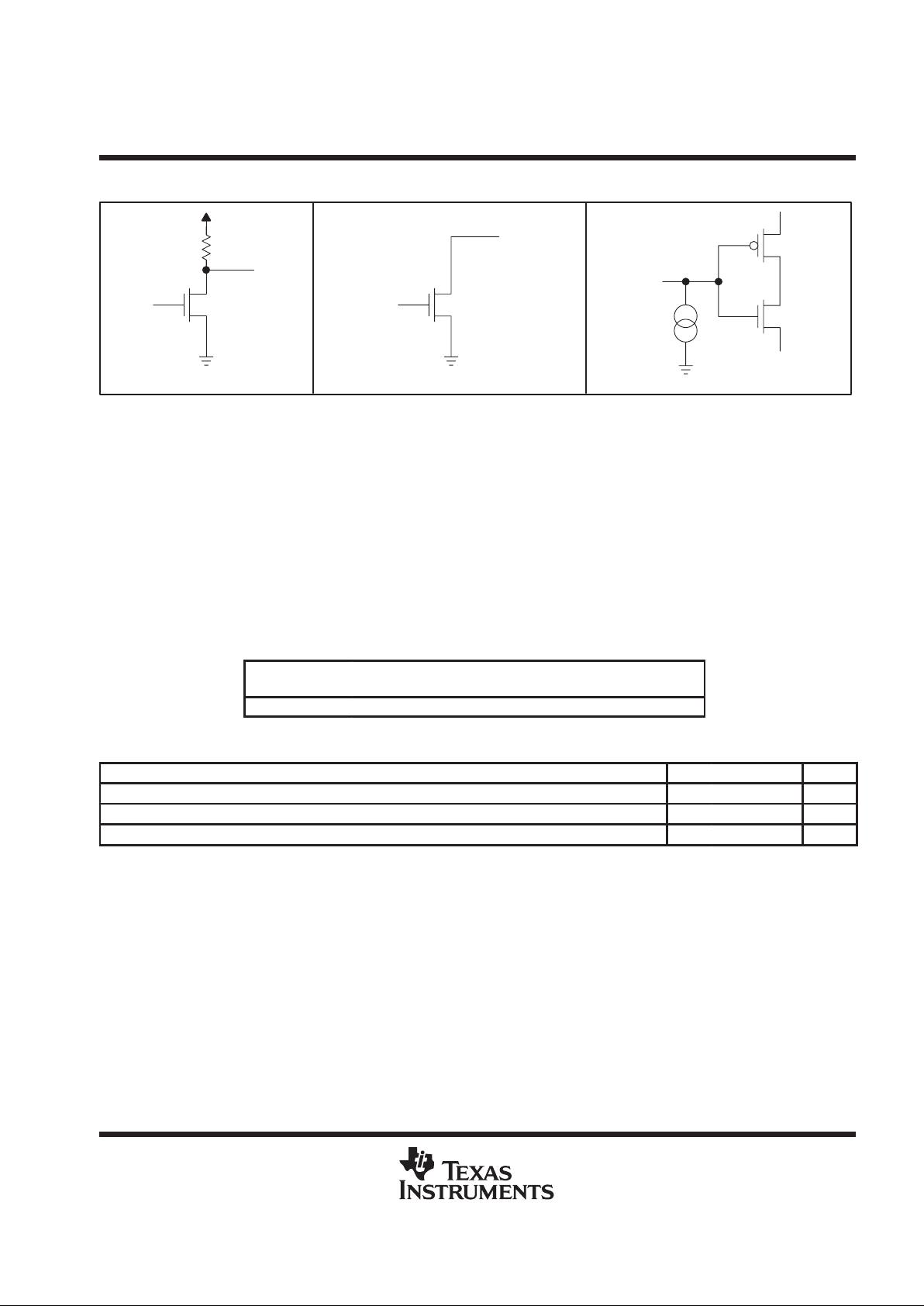
schematics of inputs and outputs
STATUS2
STATUS1
DIR/PWM
absolute maximum ratings over operating case temperature range (unless otherwise noted)
†
Power supply voltage range, V
CC
–0.3 V to 33 V. . . . . . . . . . . . . . . . . . . . . . . . . . . . . . . . . . . . . . . . . . . . . . . . . . .
Logic input voltage range, V
IN
–0.3 V to 7 V. . . . . . . . . . . . . . . . . . . . . . . . . . . . . . . . . . . . . . . . . . . . . . . . . . . . . . .
Load dump (for 400 ms, T
C
= 25°C) 40 V. . . . . . . . . . . . . . . . . . . . . . . . . . . . . . . . . . . . . . . . . . . . . . . . . . . . . . . . . .
Status output voltage range, V
O(status)
–0.3 V to 7 V. . . . . . . . . . . . . . . . . . . . . . . . . . . . . . . . . . . . . . . . . . . . . . .
Continuous power dissipation, T
C
= 25°C 25 W. . . . . . . . . . . . . . . . . . . . . . . . . . . . . . . . . . . . . . . . . . . . . . . . . . . .
Storage temperature range, T
stg
–55°C to 150°C. . . . . . . . . . . . . . . . . . . . . . . . . . . . . . . . . . . . . . . . . . . . . . . . . . .
Maximum junction temperature, T
J
150°C. . . . . . . . . . . . . . . . . . . . . . . . . . . . . . . . . . . . . . . . . . . . . . . . . . . . . . . . .
†
Stresses beyond those listed under “absolute maximum ratings” may cause permanent damage to the device. These are stress ratings only, and
functional operation of the device at these or any other conditions beyond those indicated under “recommended operating conditions” is not
implied. Exposure to absolute-maximum-rated conditions for extended periods may affect device reliability.
DISSIPATION RATING TABLE
TA ≤ 25°C
POWER RATING
DERATING FACTOR
ABOVE TA = 25°C
TA = 70°C
POWER RATING
TA = 125°C
POWER RATING
25 W –0.2 W/°C 16 W 5 W
recommended operating conditions
MIN MAX UNIT
Supply voltage, V
CC
6 18 V
Operating case temperature, T
C
–40 125 °C
Switching frequency, f
PWM
2 kHz
TPIC0107B
PWM CONTROL INTELLIGENT H-BRIDGE
SLIS067 – NOVEMBER 1998
4
POST OFFICE BOX 655303 • DALLAS, TEXAS 75265
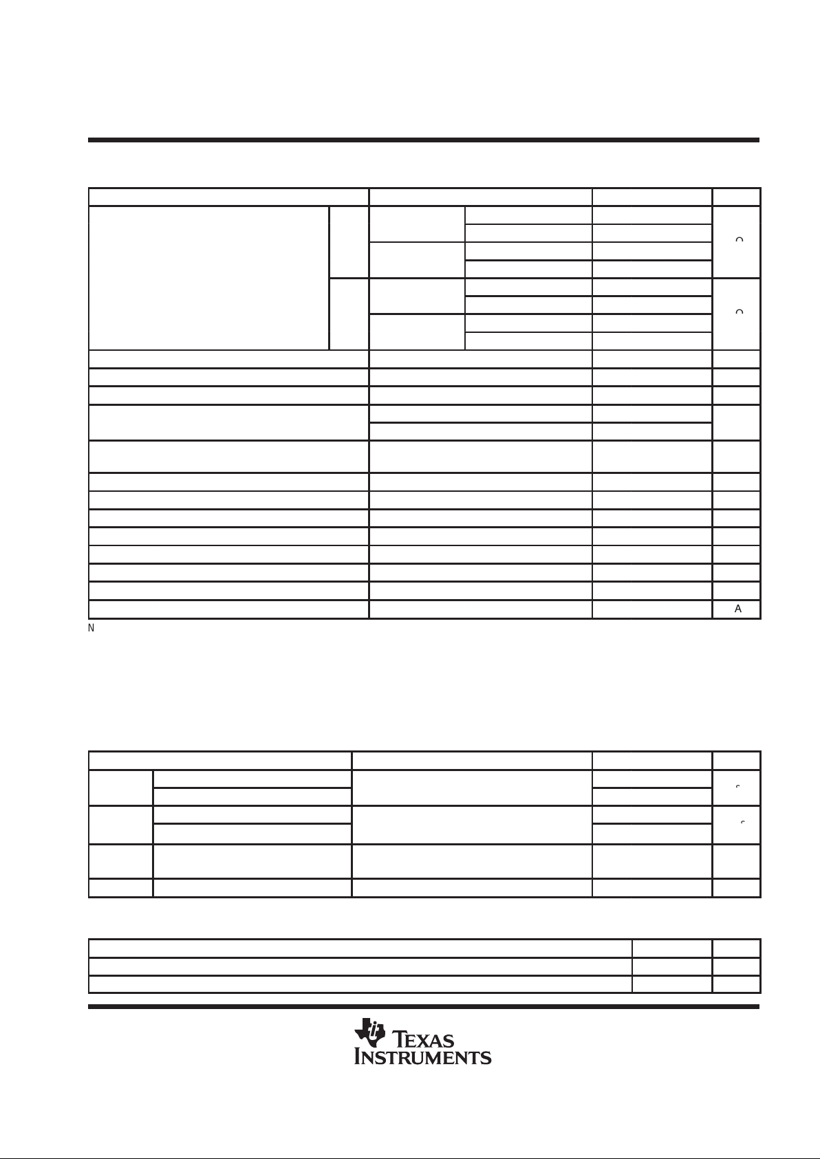
electrical characteristics over recommended operating case temperature range and V
CC
= 5 V to
6 V (unless otherwise noted)
PARAMETER TEST CONDITIONS MIN TYP MAX UNIT
TJ = 25°C 550
Static drain-source on-resistance (per transistor)
LSD
TJ = 150°C 850
mΩ
r
DS(on)
()
I
(BR)
= 1 A
TJ = 25°C 600
HSD
TJ = 150°C 870
mΩ
I
(QCD)
Open circuit detection current 10 40 100 mA
V
(UVCC(OFF))
Under voltage detection on VCC, switch off voltage See Note 1 5 V
V
(UVCC(ON))
Under voltage detection on VCC, switch on voltage See Note 1 5.2 V
V
(STL)
STATUS low output voltage IO = 100 µA, See Note 1 0.8 V
V
(ST2H)
STATUS2 high output voltage IO = 20 µA, See Note 1 3 5.4 V
I
(ST(OFF))
STATUS output leakage current V
(ST)
= 5 V, See Note 1 5 µA
V
IL
Low level logic input voltage –0.3 0.5 V
V
IH
High level logic input voltage 3.6 7 V
∆V
I
Hysteresis of input voltage 0.3 V
I
IH
High level logic input current VIH = 3.5 V 2 10 50 µA
NOTE 1: The device functions according to the function table for VCC between V
(UVCC)
and 5 V (no parameters specified). STA TUS outputs are
not defined for VCC less than V
(UVCC)
.
TPIC0107B
PWM CONTROL INTELLIGENT H-BRIDGE
SLIS067 – NOVEMBER 1998
5
POST OFFICE BOX 655303 • DALLAS, TEXAS 75265
electrical characteristics over recommended operating case temperature and supply voltage
ranges (unless otherwise noted) (see Note 2)
PARAMETER TEST CONDITIONS MIN TYP MAX UNIT
°
VCC = 6 V to 9 V 380
T
J
=
25°C
VCC = 9 V to 18 V 280 340
LSD
°
VCC = 6 V to 9 V 620
mΩ
Static drain-source on-resistance
T
J
=
150°C
VCC = 9 V to 18 V 400 560
r
DS(on)
(per transistor) IBR = 1 A
°
VCC = 6 V to 9 V 430
T
J
=
25°C
VCC = 9 V to 18 V 280 340
HSD
°
VCC = 6 V to 9 V 640
mΩ
T
J
=
150°C
VCC = 9 V to 18 V 400 560
I
(QCD)
Open circuit detection current 10 40 100 mA
T
SDS
Static thermal shutdown temperature See Notes 3 and 4 140 °C
T
SDD
Dynamic thermal shutdown temperature See Notes 3 and 5 160 ° C
VCC = 6 V to 9 V 4.8 7.5
ICSCurrent shutdown limit
VCC = 9 V to 18 V 5 7.5
A
I
(CON)
Continuous bridge current
TJ = 125°C, Operating lifetime 10,000 hours,
(see Figure 1)
3 A
V
(OVCC)
Over voltage detection on V
CC
27 36 V
V
(STL)
STATUS low output voltage IO = 100 µA 0.8 V
V
(ST2H)
STATUS2 high output voltage IO = 20 µA 3.9 5.4 V
I
(ST(OFF))
STATUS output leakage current V
(ST)
= 5 V 5 µA
V
IL
Low level logic input voltage –0.3 0.8 V
V
IH
High level logic input voltage 3.6 7 V
∆V
I
Hysteresis of input voltage 0.3 V
I
IH
High level logic input current VIH = 3.5 V 2 10 50 µ
A
NOTES: 2. The device functions according to the function table for VCC between 18 V and V
(OVCC)
, but only up to a maximum supply voltage
of 33 V (no parameters specified). Exposure beyond 18 V for extended periods may affect device reliability.
3. Exposure beyond absolute-maximum-rated condition of junction temperature may affect device reliability.
4. No temperature gradient between DMOS transistor and temperature sensor .
5. With temperature gradient between DMOS transistor and temperature sensor in a typical application (DMOS transistor as heat
source).
switching characteristics over recommended operating case temperature and supply voltage
ranges (unless otherwise noted)
PARAMETER TEST CONDITIONS MIN TYP MAX UNIT
High-side driver turn-on time
100
t
out(on)
Low-side driver turn-on time
V
DS(on)
<
1 V at 1 A
,
V
CC
=
13.2 V
100
µ
s
Slew rate, low-to-high sinusoidal (δV/δt)
1 6
SR
Slew rate, high-to-low sinusoidal (δV/δt)
V
CC
=
13.2 V
,
I
O
=
1 A resistive load
1 6
V/µs
t
d(QCD)
Under current spike duration to trigger
open circuit detection
VCC = 5 V to 18 V 1 10 ms
t
d(CS)
Delay time for over current shutdown 5 10 25 µs
thermal resistance
PARAMETER MIN MAX
UNIT
R
θJA
Junction-to-ambient thermal resistance 5 °C/W
R
θJC
Junction-to-case thermal resistance 97 °C/W

TPIC0107B
PWM CONTROL INTELLIGENT H-BRIDGE
SLIS067 – NOVEMBER 1998
6
POST OFFICE BOX 655303 • DALLAS, TEXAS 75265
PARAMETER MEASUREMENT INFORMATION
Maximum continuous bridge current versus time based on 50 FITs at 100,000 hours operating life (90%
confidence model)
5
0
01020304050601070 80 90 100
TJ = 75°C
TJ = 100°C
TJ = 125°C
TJ = 150°C
– Continuous Bridge Current – A
I
(CON)
t – Time × 1000-h
Figure 1. Electromigration Reliability Data
Example:
Average continuous bridge current, I
CON
Average junction temperature, TJOperating lifetime of device based on electromigration
2 A 125°C >20,000 h
3 A 125°C >10,000 h

TPIC0107B
PWM CONTROL INTELLIGENT H-BRIDGE
SLIS067 – NOVEMBER 1998
7
POST OFFICE BOX 655303 • DALLAS, TEXAS 75265
PARAMETER MEASUREMENT INFORMATION
operating wave forms
<1 ms (min.)
DIR (Low)
PWM
STATUS1
STATUS2
OUT1 (High)
OUT2
Open Circuit
Figure 2. Open Circuit
DIR (Low)
PWM
STATUS1
STATUS2
OUT1
OUT2
Short Circuit
I
LIM
Bridge Current
Figure 3. Short Circuit (e.g., OUT2 to V
CC
)

TPIC0107B
PWM CONTROL INTELLIGENT H-BRIDGE
SLIS067 – NOVEMBER 1998
8
POST OFFICE BOX 655303 • DALLAS, TEXAS 75265
PARAMETER MEASUREMENT INFORMATION
operating wave forms (continued)
DIR (Low)
PWM
STATUS1
STATUS2
OUT1
OUT2
Over Temperature
Figure 4. Over Temperature
DIR
Brake
Counter-
Clockwise
Rotation
Clockwise
Rotation
PWM
STATUS1 (High)
STATUS2 (High)
OUT1
OUT2
Brake Brake
Figure 5. No Fault

TPIC0107B
PWM CONTROL INTELLIGENT H-BRIDGE
SLIS067 – NOVEMBER 1998
9
POST OFFICE BOX 655303 • DALLAS, TEXAS 75265
PRINCIPLES OF OPERATION
protective functions and diagnostics
†
over current/short circuit
‡
The TPIC0107B detects shorts to VCC, ground, or across the load being driven, by comparing the VDS voltage
drop across the DMOS outputs against the threshold voltage. The DMOS outputs of the TPIC0107B will be
disabled and the fault flags will be generated 10 µs after an over-current or short-circuit fault is detected. This
10 µs delay is long enough to serve as a de-glitch filter for high current transients, yet short enough to prevent
damage to the DMOS outputs. The DMOS outputs remain latched off until either DIR or PWM input is toggled.
In cases where the outputs have a continuous short-to-ground with a current rise time faster than 0.5 A/µs, the
over-current shutdown threshold will decrease to 3 A to reduce power dissipation. This reduction to 3 A is
achieved since the DMOS outputs will not be fully enhanced when the over-current threshold is reached if the
current rise time exceeds 0.5 A/µs. Over-current and/or short-circuit protection is provided up to V
CC
= 16.5 V
and a junction temperature of 90°C.
over temperature
The TPIC0107B disables all DMOS outputs and the fault flags will be set when T
J
≥140°C (min.). The DMOS
outputs remain latched off until either DIR or PWM input is toggled.
under voltage
The TPIC0107B disables all DMOS outputs when V
CC
≤V
(UVCC)
. The outputs will be re-enabled when
V
CC
≥V
(UVCC)
. No fault flags are set when under-voltage lockout occurs.
over voltage
In order to protect the DMOS outputs from damage caused by excessive supply voltage, the TPIC0107B
disables all outputs when V
CC
≥V
(OVCC)
. Once VCC ≤V
(OVCC)
, either DIR or PWM input must be toggled to
re-enable the DMOS outputs.
cross conduction
Monitoring circuitry for each transistor detects whether the particular transistor is active to prevent the HSD or
LSD of the corresponding half H-bridge from conducting.
open circuit
During operation, the bridge current is controlled continuously . If the bridge current is >10 mA (min.) for a period
>1 ms (min.), the fault flags are set. However, the output transistors will not be disabled.
†
All limits mentioned are typical values unless otherwise noted.
‡
If a short circuit occurs (i.e., the over-current detection circuitry is activated) at a supply voltage higher than 16.5 V and a junction temperature
higher than 90°C, damage to the device may occur.

TPIC0107B
PWM CONTROL INTELLIGENT H-BRIDGE
SLIS067 – NOVEMBER 1998
10
POST OFFICE BOX 655303 • DALLAS, TEXAS 75265
PRINCIPLES OF OPERATION
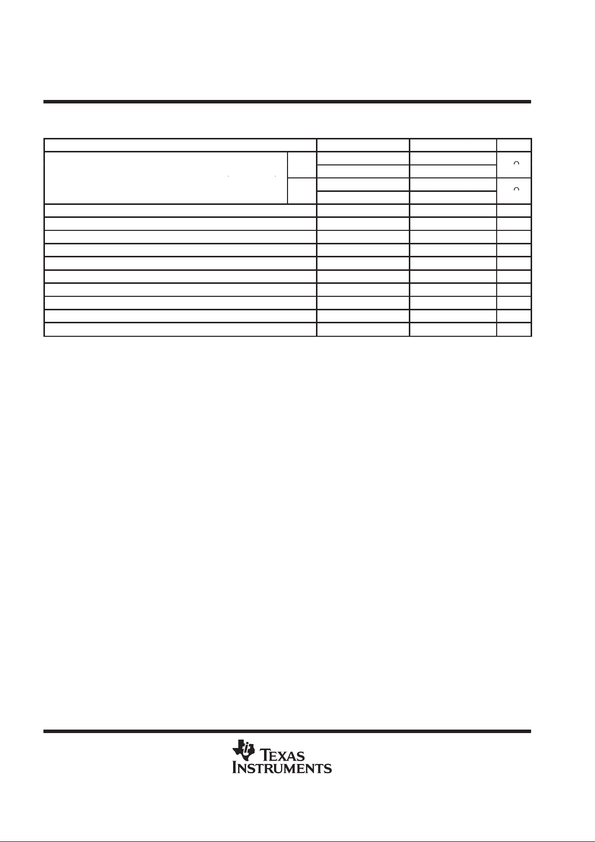
DIAGNOSTICS TABLE (see Note 6)
FLAG
DIR PWM OUT1 OUT2 STATUS1†STATUS2
Normal operation
0
0
1
1
0
1
0
1
HS
HS
HS
LS
HS
LS
HS
HS
1
1
1
1
1
1
1
1
Open circuit between OUT1 and OUT2
0
0
1
1
0
1
0
1
HS
HS
HS
LS
HS
LS
HS
HS
1
0
1
0
1
0
1
0
Short circuit from OUT1 to OUT2 (see Notes 7 and 8)
0
1
1
1
X
X
X
X
0
0
0
0
Short circuit from OUT1 to GND (see Notes 7 and 8)
0
1
0
0
0
1
X
X
X
X
X
X
0
0
0
0
0
0
Short circuit from OUT2 to GND (see Notes 7 and 8)
0
1
1
0
0
1
X
X
X
X
X
X
0
0
0
0
0
0
Short circuit from OUT1 to VCC (see Notes 7 and 8) 1 1 X X 0 0
Short circuit from OUT2 to VCC (see Notes 7 and 8) 0 1 X X 0 0
Over temperature
0
0
1
1
0
1
0
1
Z
Z
Z
Z
Z
Z
Z
Z
0
0
0
0
0
0
0
0
†
When wired with a pull-up resistor
SYMBOL V ALUE
0 Logic low
1 Logic high
HS High-side MOSFET conducting
LS Low-side MOSFET conducting
Z No output transistors conducting
X Voltage level undefined
NOTES: 6. All input combinations not stated result in STATUS output = 1.
7. STA TUS1 active for a minimum of 3 µs.
8. STA TUS2 active until an input is toggled.

TPIC0107B
PWM CONTROL INTELLIGENT H-BRIDGE
SLIS067 – NOVEMBER 1998
11
POST OFFICE BOX 655303 • DALLAS, TEXAS 75265
TYPICAL CHARACTERISTICS
Figure 6
200
100
0
–40 –20 0 20 40 60 80
– Static Drain-Source On-Resistance – m
300
STATIC DRAIN-SOURCE ON-RESISTANCE
vs
JUNCTION TEMPERATURE
400
100 120 140
VCC = 9.18 V
Ω
r
DS(on)
TJ – Junction Temperature – °C
Figure 7
300
200
100
0
0 5 10 15
400
500
STATIC-DRAIN-SOURCE ON-RESISTANCE
vs
SUPPLY VOLTAGE
600
20 25
VCC – Supply Voltage – V
HSD, TJ = 125°C
LSD, TJ = 125°C
LSD, TJ = 25°C
HSD, TJ = 25°C
– Static Drain-Source On-Resistance – mΩ
r
DS(on)
Figure 8
10
5
0
–40 –20 0 20 40 60 80
– Output Stage Turn-On Time –
15
OUTPUT STAGE TURN-ON TIME
vs
JUNCTION TEMPERATURE
20
100 120 140
sµ
t
out(on)
HSD, VCC = 13.2 V
LSD, VCC = 13.2 V
TJ – Junction Temperature – °C

TPIC0107B
PWM CONTROL INTELLIGENT H-BRIDGE
SLIS067 – NOVEMBER 1998
12
POST OFFICE BOX 655303 • DALLAS, TEXAS 75265
APPLICATION INFORMATION
†
Necessary for isolating supply voltage or interruption (e.g., 47 µF).
V
CC
M
CONTROL DIAGNOSTIC
Microcontroller
DIR
PWM
STATUS1
STATUS2
GND GNDS
OUT1
OUT2
V
CC
TPIC0107B
100 kΩ
5 V
100 nF
47 µF
†
NOTE: If a STATUS output is not connected to the appropriate microcontroller input, it shall remain unconnected.

TPIC0107B
PWM CONTROL INTELLIGENT H-BRIDGE
SLIS067 – NOVEMBER 1998
13
POST OFFICE BOX 655303 • DALLAS, TEXAS 75265
MECHANICAL DATA
DWP (R-PDSO-G**) PowerPAD PLASTIC SMALL-OUTLINE PACKAGE
Gage Plane
0.419 (10,65)
0.400 (10,16)
0.010 (0,25) NOM
Thermal Pad
(See Note D)
0.010 (0,25)
0.016 (0,40)
0.050 (1,27)
Seating Plane
4147575/A 02/98
11
10
A
20-PIN SHOWN
20
1
0.104 (2,65) MAX
0.293 (7,45)
0.299 (7,59)
0.020 (0,51)
0.014 (0,35)
0.004 (0,10)
M
0.010 (0,25)
0.050 (1,27)
0°–8°
0.710
28
0.510200.610
24
0.700
(18,03)
(17,78)
0.500
(15,49)
(15,24)
0.600
0.410
16
DIM
PINS **
(10,41)
(10,16)
0.400
A MIN
A MAX
(12,95)
(12,70)
0.006 (0,15)
0.002 (0,05)
NOTES: A. All linear dimensions are in inches (millimeters).
B. This drawing is subject to change without notice.
C. Body dimensions do not include mold flash or protrusion not to exceed 0.006 (0,15).
D. The package thermal performance may be enhanced by bonding the thermal pad to an external thermal plane. This pad is electrically
and thermally connected to the backside of the die and possibly selected leads.
PowerPAD is a trademark of Texas Instruments Incorporated.

IMPORTANT NOTICE
T exas Instruments and its subsidiaries (TI) reserve the right to make changes to their products or to discontinue
any product or service without notice, and advise customers to obtain the latest version of relevant information
to verify, before placing orders, that information being relied on is current and complete. All products are sold
subject to the terms and conditions of sale supplied at the time of order acknowledgement, including those
pertaining to warranty, patent infringement, and limitation of liability.
TI warrants performance of its semiconductor products to the specifications applicable at the time of sale in
accordance with TI’s standard warranty. Testing and other quality control techniques are utilized to the extent
TI deems necessary to support this warranty. Specific testing of all parameters of each device is not necessarily
performed, except those mandated by government requirements.
CERT AIN APPLICATIONS USING SEMICONDUCTOR PRODUCTS MAY INVOLVE POTENTIAL RISKS OF
DEATH, PERSONAL INJURY, OR SEVERE PROPERTY OR ENVIRONMENTAL DAMAGE (“CRITICAL
APPLICATIONS”). TI SEMICONDUCTOR PRODUCTS ARE NOT DESIGNED, AUTHORIZED, OR
WARRANTED TO BE SUITABLE FOR USE IN LIFE-SUPPORT DEVICES OR SYSTEMS OR OTHER
CRITICAL APPLICATIONS. INCLUSION OF TI PRODUCTS IN SUCH APPLICA TIONS IS UNDERST OOD TO
BE FULLY AT THE CUSTOMER’S RISK.
In order to minimize risks associated with the customer’s applications, adequate design and operating
safeguards must be provided by the customer to minimize inherent or procedural hazards.
TI assumes no liability for applications assistance or customer product design. TI does not warrant or represent
that any license, either express or implied, is granted under any patent right, copyright, mask work right, or other
intellectual property right of TI covering or relating to any combination, machine, or process in which such
semiconductor products or services might be or are used. TI’s publication of information regarding any third
party’s products or services does not constitute TI’s approval, warranty or endorsement thereof.
Copyright 1998, Texas Instruments Incorporated
 Loading...