

Page 1
User's Guide
SLVUAU1–October 2016
TPD8S300 Evaluation Module
This user's guide describes the characteristics, operation, and use of the TPD8S300 evaluation module
(EVM). This EVM is a TPD8S300 integrated chip set into a USB Type-C passthrough board to allow the
user to test the operation of the TPD8S300 overvoltage protection and ESD protection in their own
system. This user's guide includes setup instructions, schematic diagrams, a bill of materials, and printedcircuit board layout drawings for the EVM.
Contents
1 Introduction ................................................................................................................... 2
2 Board Setup .................................................................................................................. 2
2.1 Overvoltage Protection Testing ................................................................................... 2
2.2 ESD Testing ......................................................................................................... 3
3 Schematic..................................................................................................................... 4
4 Board Layout ................................................................................................................. 5
5 Bill of Materials............................................................................................................... 7
List of Figures
1 CC1 Line Short to 20-V Waveform........................................................................................ 3
2 TPD8S300EVM .............................................................................................................. 3
3 TPD8S300EVM Schematic................................................................................................. 4
4 Top Layer .................................................................................................................... 5
5 Ground Plane 1 ............................................................................................................. 5
6 Midlayer 1..................................................................................................................... 5
7 Ground Plane 2 ............................................................................................................. 5
8 Power Plane 1................................................................................................................ 5
9 Midlayer 2..................................................................................................................... 5
10 Ground Plane 3 .............................................................................................................. 6
11 Bottom Layer ................................................................................................................. 6
1 Bill of Materials............................................................................................................... 7
SLVUAU1–October 2016
Submit Documentation Feedback
List of Tables
Copyright © 2016, Texas Instruments Incorporated
TPD8S300 Evaluation Module
1
Page 2

Introduction
1 Introduction
Texas Instrument’s TPD8S300 evaluation module helps designers evaluate the operation and
performance of the TPD8S300 device. The TPD8S300 is a single-chip solution for protection of the USB
Type-C configuration channel (CC), sideband use channel (SBU), and D± data lines. The device provides
Short-to-VBUS Over Voltage Protection up to 22 V for CC1, CC2, SBU1, and SBU2 pins to prevent
damage caused by a faulty connecter or mechanical twist shorting pins. The TPD8S300 also provides 8channels of IEC 61000-4-2 ESD protection for CC1, CC2, SBU1, SBU2, D± (Top Side), and D± (Bottom
Side) pins of the USB Type-C connecter.
2 Board Setup
The pass-through EVM allows the user to ensure that the TPD8S300 will not impede typical operation of
their USB port while also allowing the user to test the TPD8S300 protection during an overvoltage or ESD
event.
To test the TPD8S300 EVM, plug the male (“system side”, J1) connector on the EVM into a USB Type-C
female port and plug a typical USB Type-C cable or peripheral into the EVM’s female connector
(“connector side”, J2). The TPD8S300 is intended to be placed very close to the port in a typical system,
so this setup will closely simulate a designed in TPD8S300. When plugged in, the user can ensure that
the TPD8S300 will not impede standard USB operation.
The 0 Ω resistors R2 and R3 allow the user to determine whether the TPD8S300 dead battery resistors
are active. By default, the resistors will short the CC1 and CC2 pins to the RPD_G1 and RPD_G2 pins
and enable the dead battery resistor function, allowing the TPD8S300 to serve as either a UFP or a DFP
port. To simulate a use case where the TPD8S300 will not function as a UFP, turn off the dead battery
functionality by manually removing these resistors.
www.ti.com
The EVM requires 3.3 V between the Vpwr (TP1) and Ground (TP3) pins to power up the TPD8S300. If
the system supports USB charging from a dead battery condition, it is recommended that the EVM be
powered from the protected USB Controller to show that the dead battery functionality works properly. The
EVM includes a 0.1uF (C2) capacitor to ground on the Vbias pin of the TPD8S300, a 100-kΩ (R1) resistor
to Vpwr on the FLT pin, and a 1-uF (C1) capacitor to ground on the Vpwr pin. These are recommended
for proper operation of the TPD8S300 in all applications.
2.1 Overvoltage Protection Testing
The EVM is designed to allow the user to ensure that the TPD8S300 can protect their system from
overvoltage events. By shorting either a CC line or SBU line to a high voltage on the connecter side of the
EVM, the user can confirm that the TPD8S300 will protect their system. The short can be created by
applying 20 V to one of the protected lines on a USB Type-C breakout board plugged into J2 or by using a
custom board that discharges 20 V over a capacitor when plugged in. When the TPD8S300 sees a
voltage over the overvoltage threshold on a protected line it will isolate all four CC and SBU lines within
100 ns to protect the system. Use an oscilloscope to measure the voltage on both the system side and the
connector side of the EVM to view the clamped voltage that the protected system is seeing.
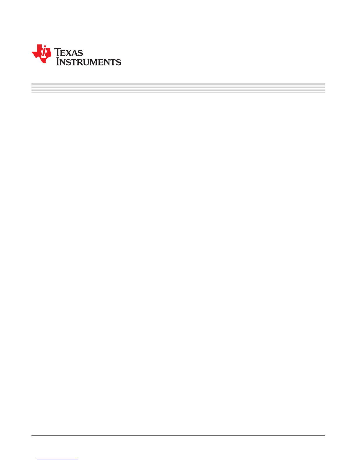
The waveform in Figure 1, where channel one is the system side of the TPD8S300EVM and channel two
is the connector side, was taken when CC1 from a TPD8S300EVM in DFP mode in series with a
TPD8S300EVM was shorted to a 24-V Vbus line. The event was created by a plugging in a one foot cable
to a custom USB Type-C board that simulates a faulty peripheral, pulling Vbus to 24 V and discharging
the voltage to the CC line over a capacitor. Measuring the voltage over the TPD8S300EVM shows the
device clamping the overvoltage event to a maximum voltage of 7.5 V and completely isolating the
controller within 60 ns.
2
TPD8S300 Evaluation Module
Copyright © 2016, Texas Instruments Incorporated
SLVUAU1–October 2016
Submit Documentation Feedback
Page 3
www.ti.com
2.2 ESD Testing
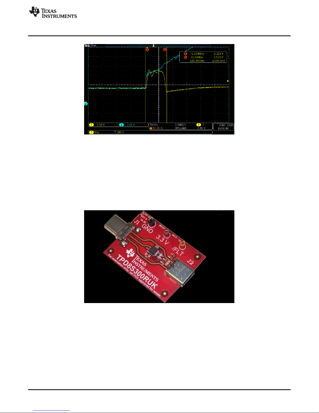
Figure 2 shows the TPD8S300EVM. The EVM has four ESD test points, one on each CC and SBU line,
that allow the user to use a ESD simulator in either contact or air-gap test mode to measure the ESD
protection provided by the TPD8S300. Probe points one and two correspond to the SBU2 and SBU1 lines
respectively. Probe points four and five correspond to the CC1 and CC2 lines respectively. To measure
the ESD response on the D± lines use an ESD simulator on the respective points on a break-out board
plugged into J2. Refer to the application report, IEC 61000-4-x Tests for TI’s Protection Devices for
specifics on proper ESD testing methods.
Board Setup
Figure 1. CC1 Line Short to 20-V Waveform
SLVUAU1–October 2016
Submit Documentation Feedback
Figure 2. TPD8S300EVM
Copyright © 2016, Texas Instruments Incorporated
TPD8S300 Evaluation Module
3
Page 4

Schematic
3 Schematic
www.ti.com
4
TPD8S300 Evaluation Module
Figure 3. TPD8S300EVM Schematic
Copyright © 2016, Texas Instruments Incorporated
SLVUAU1–October 2016
Submit Documentation Feedback
Page 5

www.ti.com
4 Board Layout
This section provides the TPD8S300EVM board layout. The TPD8S300 is an 8-layer board of FR-4 at
0.032" thickness.
Board Layout
Figure 4. Top Layer
Figure 5. Ground Plane 1
Figure 6. Midlayer 1
SLVUAU1–October 2016
Submit Documentation Feedback
Copyright © 2016, Texas Instruments Incorporated
Figure 7. Ground Plane 2
TPD8S300 Evaluation Module
5
Page 6

Board Layout
www.ti.com
Figure 8. Power Plane 1
Figure 9. Midlayer 2
Figure 10. Ground Plane 3 Figure 11. Bottom Layer
6
TPD8S300 Evaluation Module
Copyright © 2016, Texas Instruments Incorporated
SLVUAU1–October 2016
Submit Documentation Feedback
Page 7

www.ti.com
5 Bill of Materials
Bill of Materials
Table 1. Bill of Materials
Design
ator
C1 1 1 uF CAP, CERM, 1 uF, 35 V,
C2 1 0.1 uF CAP, CERM, 0.1uF, 50
J1 1 Plug, USB3.1 Type C,
J2 1 Receptacle, 0.5 mm,
R1 1 100 kΩ RES, 100 k, 5%, 0.1 W,
R2, R3 2 0 RES, 0, 5%, 0.1 W,
TP1 1 Test Point, Miniature,
TP2 1 Test Point, Miniature,
TP3 1 Test Point, Compact,
U1 1 USB Type C Interface
Quantity Value Description Package
±10%, JB, 0402
V, ±10%, X7R, AECQ200 Grade 1, 0402
24 V Position, R/A, SMT
USB TYPE C, R/A, SMT
AEC-Q200 Grade 0,
0402
0603
Red, TH
Orange, TH
Black, TH
Protector: Short-to-
VBUS Over Voltage and
IEC 61000-4-2 ESD
Protection, RUK0020b
Reference
0402 C1005JB1V105K05
0402 GCM155R71H104
Plug, USB3.1
Type C, 24 V
Position, R/A,
SMT
Receptacle,
.5mm, USB
TYPE C, R/A,
SMT
0402 ERJ-2GEJ104X Panasonic
0603 CRCW06030000Z0EAVishay-Dale
Red Miniature
Testpoint
Orange
Miniature
Testpoint
Black Compact
Testpoint
RUK0020B TPD8S300RUK Texas
Part Number Manufacturer
0BC
MuRata
KE02D
DX07P024MJ1R1500JAE Electronics
12401610E4#2A Amphenol
Canada
5000 Keystone
5003 Keystone
5006 Keystone
Instruments
TDK
SLVUAU1–October 2016
Submit Documentation Feedback
Copyright © 2016, Texas Instruments Incorporated
TPD8S300 Evaluation Module
7
Page 8

IMPORTANT NOTICE
Texas Instruments Incorporated and its subsidiaries (TI) reserve the right to make corrections, enhancements, improvements and other
changes to its semiconductor products and services per JESD46, latest issue, and to discontinue any product or service per JESD48, latest
issue. Buyers should obtain the latest relevant information before placing orders and should verify that such information is current and
complete. All semiconductor products (also referred to herein as “components”) are sold subject to TI’s terms and conditions of sale
supplied at the time of order acknowledgment.
TI warrants performance of its components to the specifications applicable at the time of sale, in accordance with the warranty in TI’s terms
and conditions of sale of semiconductor products. Testing and other quality control techniques are used to the extent TI deems necessary
to support this warranty. Except where mandated by applicable law, testing of all parameters of each component is not necessarily
performed.
TI assumes no liability for applications assistance or the design of Buyers’ products. Buyers are responsible for their products and
applications using TI components. To minimize the risks associated with Buyers’ products and applications, Buyers should provide
adequate design and operating safeguards.
TI does not warrant or represent that any license, either express or implied, is granted under any patent right, copyright, mask work right, or
other intellectual property right relating to any combination, machine, or process in which TI components or services are used. Information
published by TI regarding third-party products or services does not constitute a license to use such products or services or a warranty or
endorsement thereof. Use of such information may require a license from a third party under the patents or other intellectual property of the
third party, or a license from TI under the patents or other intellectual property of TI.
Reproduction of significant portions of TI information in TI data books or data sheets is permissible only if reproduction is without alteration
and is accompanied by all associated warranties, conditions, limitations, and notices. TI is not responsible or liable for such altered
documentation. Information of third parties may be subject to additional restrictions.
Resale of TI components or services with statements different from or beyond the parameters stated by TI for that component or service
voids all express and any implied warranties for the associated TI component or service and is an unfair and deceptive business practice.
TI is not responsible or liable for any such statements.
Buyer acknowledges and agrees that it is solely responsible for compliance with all legal, regulatory and safety-related requirements
concerning its products, and any use of TI components in its applications, notwithstanding any applications-related information or support
that may be provided by TI. Buyer represents and agrees that it has all the necessary expertise to create and implement safeguards which
anticipate dangerous consequences of failures, monitor failures and their consequences, lessen the likelihood of failures that might cause
harm and take appropriate remedial actions. Buyer will fully indemnify TI and its representatives against any damages arising out of the use
of any TI components in safety-critical applications.
In some cases, TI components may be promoted specifically to facilitate safety-related applications. With such components, TI’s goal is to
help enable customers to design and create their own end-product solutions that meet applicable functional safety standards and
requirements. Nonetheless, such components are subject to these terms.
No TI components are authorized for use in FDA Class III (or similar life-critical medical equipment) unless authorized officers of the parties
have executed a special agreement specifically governing such use.
Only those TI components which TI has specifically designated as military grade or “enhanced plastic” are designed and intended for use in
military/aerospace applications or environments. Buyer acknowledges and agrees that any military or aerospace use of TI components
which have not been so designated is solely at the Buyer's risk, and that Buyer is solely responsible for compliance with all legal and
regulatory requirements in connection with such use.
TI has specifically designated certain components as meeting ISO/TS16949 requirements, mainly for automotive use. In any case of use of
non-designated products, TI will not be responsible for any failure to meet ISO/TS16949.
Products Applications
Audio www.ti.com/audio Automotive and Transportation www.ti.com/automotive
Amplifiers amplifier.ti.com Communications and Telecom www.ti.com/communications
Data Converters dataconverter.ti.com Computers and Peripherals www.ti.com/computers
DLP® Products www.dlp.com Consumer Electronics www.ti.com/consumer-apps
DSP dsp.ti.com Energy and Lighting www.ti.com/energy
Clocks and Timers www.ti.com/clocks Industrial www.ti.com/industrial
Interface interface.ti.com Medical www.ti.com/medical
Logic logic.ti.com Security www.ti.com/security
Power Mgmt power.ti.com Space, Avionics and Defense www.ti.com/space-avionics-defense
Microcontrollers microcontroller.ti.com Video and Imaging www.ti.com/video
RFID www.ti-rfid.com
OMAP Applications Processors www.ti.com/omap TI E2E Community e2e.ti.com
Wireless Connectivity www.ti.com/wirelessconnectivity
Mailing Address: Texas Instruments, Post Office Box 655303, Dallas, Texas 75265
Copyright © 2016, Texas Instruments Incorporated
 Loading...