

Page 1
User's Guide
SLVUAU3–January 2017
TPD2S701-Q1 Evaluation Module
This user's guide describes the characteristics, operation, and use of the TPD2S701-Q1 USB 2.0 Data
Line Overvoltage Protection Evaluation Module (EVM). The TPD2S701-Q1 is a 2-Channel Data Line
Short-to-Battery, Short-to-VBUS, and IEC61000-4-2 ESD protection device for automotive high-speed
interfaces like USB2.0. This EVM contains multiple TPD2S701-Q1 devices in various configurations to
allow the user to test the operation of the TPD2S701-Q1 overvoltage protection and ESD protection in
their own system. This user's guide includes setup instructions, schematic diagrams, a bill of materials,
and printed circuit board layout drawings for the EVM.
Contents
1 Introduction ................................................................................................................... 2
2 Board Setup .................................................................................................................. 2
2.1 Device Information.................................................................................................. 2
2.2 Passthrough Evaluation............................................................................................ 3
2.3 Bandwidth Evaluation .............................................................................................. 4
2.4 IEC ESD Evaluation ................................................................................................ 4
3 Schematics ................................................................................................................... 6
4 Layout ......................................................................................................................... 7
5 Bill of Materials............................................................................................................... 8
List of Figures
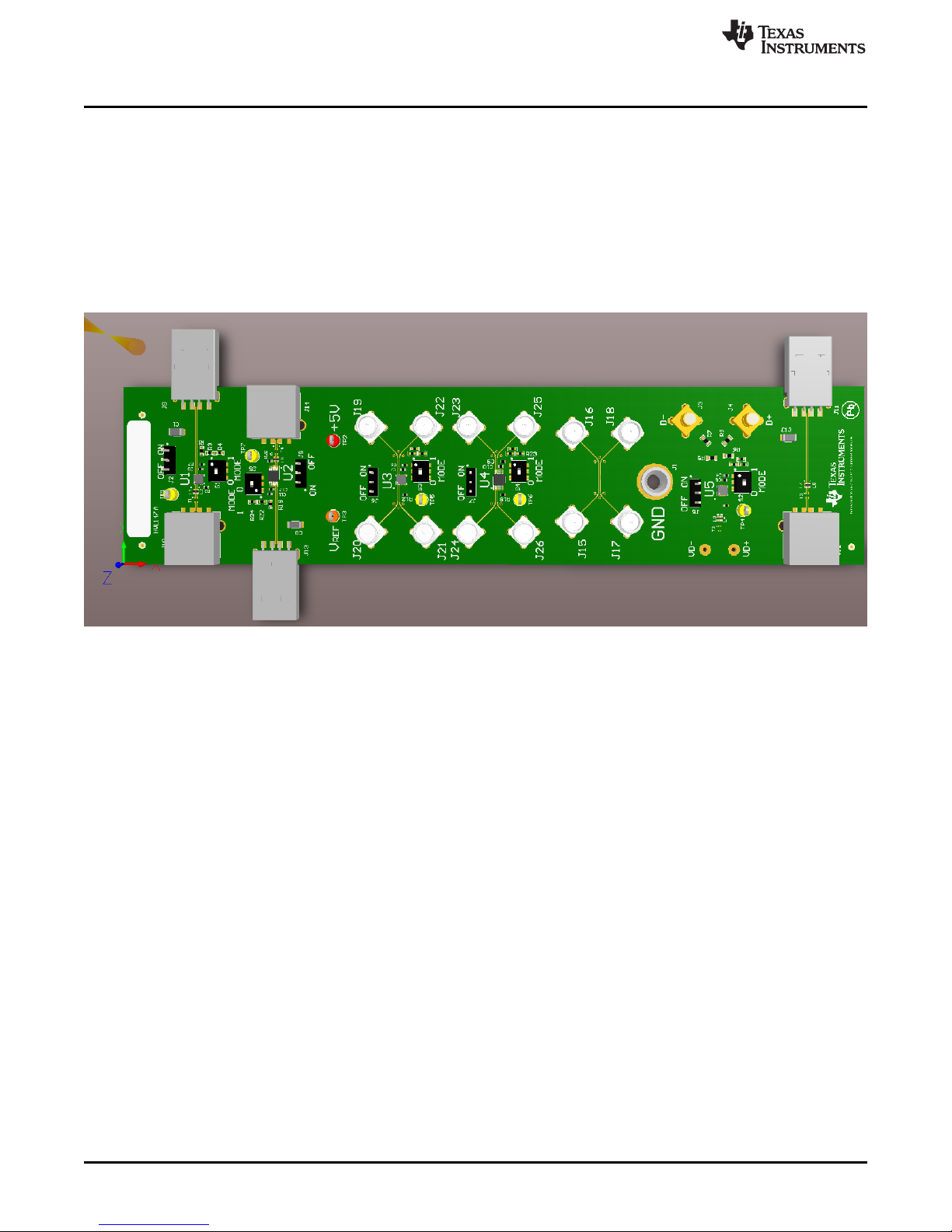
1 TPD2S701-Q1 EVM......................................................................................................... 2
2 Passthrough Evaluation Configuration.................................................................................... 3
3 Bandwidth Evaluation Configuration ...................................................................................... 4
4 ESD Evaluation Configuration ............................................................................................. 5
5 Schematic Page 1 ........................................................................................................... 6
6 Schematic Page 2 ........................................................................................................... 6
7 Schematic Page 3 ........................................................................................................... 6
8 TPD2S701-Q1 Top Layer .................................................................................................. 7
9 TPD2S701-Q1 Bottom Layer............................................................................................... 7
List of Tables
1 Bill of Materials............................................................................................................... 8
SLVUAU3–January 2017
Submit Documentation Feedback
Copyright © 2017, Texas Instruments Incorporated
TPD2S701-Q1 Evaluation Module
1
Page 2
Introduction
1 Introduction
Texas Instrument’s TPD2S701-Q1 evaluation module helps designers evaluate the operation and
performance of the TPD2S701-Q1 device. The TPD2S701-Q1 contains two data line nFET switches which
ensure safe data communication while protecting the internal system circuits from any over-voltage
conditions at the VD+ and VD– pins. See Figure 1. On these pins, this device can handle over-voltage
protection up to 18-V DC. This provides sufficient protection for shorting the data lines to the car battery
as well as the USB VBUS rail. This EVM allows the user to evaluate the operation of this device in a passthrough application, as well as to measure the ESD response and bandwidth of the device. In addition,
this EVM offer, contains the device in both the DSK and DGS package offering, so that the device can be
evaluated regardless of the preferred package option.
www.ti.com
2 Board Setup
The TPD2S701-Q1 EVM consists of 5 devices allowing for three different test setups.
2.1 Device Information
To power the EVM, apply 5 V to the pin labeled '+5V' on the EVM. If the user is testing a device in Mode
0, they will need to apply an additional voltage to the pin labeled 'Vref', but if testing is done in Mode 1
then the 'Vref' pin can be left unused. The functional devices modes are discussed in greater depth later,
but for detailed information see the device data sheet.
Each TPD2S701-Q1 in this EVM contains headers for enabling the device and a mode switch to enable
each mode of operation. Before using any of the devices, ensure that the particular device has a header
between the center pin and the pin labeled 'On' for the corresponding set of pins. It is recommended that
any devices not currently in use be disabled by moving the header between the center pin and the 'Off'
pin.
In addition, the EVM allows testing of each device in either functional mode 0 or functional mode 1 by
moving the switch corresponding to the device. The functional mode changes how the overvoltage set
point of the TPD2S701-Q1 is determined. In order to operate properly, the device must be power-cycled
when changing functional modes. We recommend only changing device modes while there is no power
applied to the '+5V' board power to ensure that the device works properly.
In functional mode 0 the overvoltage set point is determined by an external voltage applied to the 'Vref' pin
on the EVM. The correlation between the Vref voltage and the overvoltage set point is determined by a
formula that can be found in the device datasheet. The voltage applied to the 'Vref' pin applies to all
TPD2S701-Q1 devices on the EVM that are currently enabled and in mode 0.
Figure 1. TPD2S701-Q1 EVM
2
TPD2S701-Q1 Evaluation Module
Copyright © 2017, Texas Instruments Incorporated
SLVUAU3–January 2017
Submit Documentation Feedback
Page 3
www.ti.com
If the switch is placed in position 1, the overvoltage set point is determined instead by external resistors
and an internal voltage reference. In this mode, the device can operate with no external voltage applied to
the 'Vref' pin. The EVM is designed with external resistors to always have a 3.6 V overvoltage set point in
mode 1.
Each device also contains a yellow test point that allows the user to measure the corresponding devices
FLT output. Measure the voltage on this pin to record when the device goes into an undervoltage,
overvoltage, or thermal shutdown state to ensure that the device operates as expected.
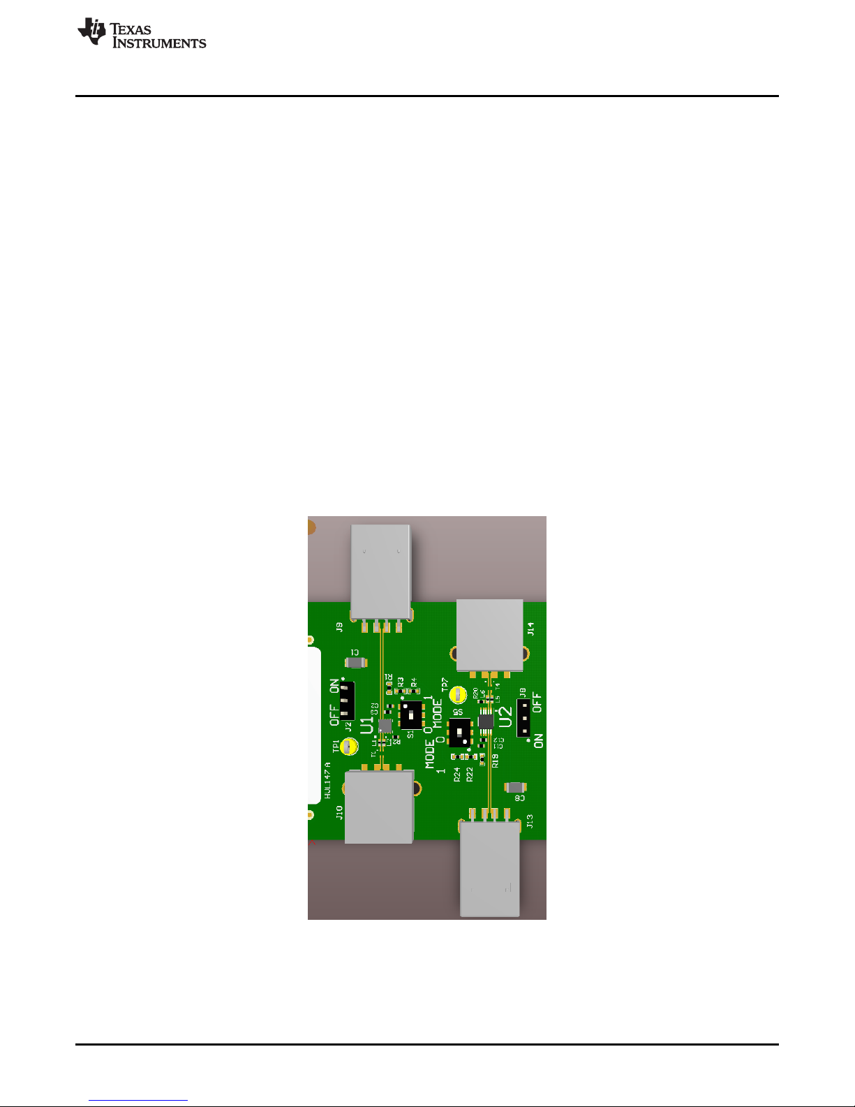
2.2 Passthrough Evaluation
Devices U1 and U2 are in a configured to allow for USB 2.0 pass-through testing. The two devices are in
a DSK and DGS package respectively, but otherwise are functionality identical. Each has a male and
female USB port that can be plugged into any system with a USB 2.0 port to ensure that the device can
protect existing systems. Plug J9 or J13 into a USB port and then plug a peripheral into J10 or J14 to
ensure that during typical operation the TPD2S701-Q1 has no effect on standard USB operations. While
plugged in, use a probe to apply a voltage above the overvoltage setpoint to one of the data lines and
observe that the TPD2S701-Q1 isolates the system, preventing any data pass-through. After the voltage is
removed, the TPD2S701-Q1 must remove the isolation and quickly re-allow data communications. See
Figure 2.
By taking advantage of this pass-through evaluation, the user can quickly determine whether the
TPD2S701-Q1 is optimal for their existing system without requiring any board changes or non-optimal test
setups. There is an additional USB 2.0 pass-through setup at the bottom of the board that is designed for
calibration. The board and trace add some parasitics and bandwidth loss that do not reflect how the
TPD2S701-Q1 operates when designed into a system. This additional pass-through allows for calibration
to account for those and get a more accurate picture of the TPD2S701-Q1.
Board Setup
Figure 2. Passthrough Evaluation Configuration
SLVUAU3–January 2017
Submit Documentation Feedback
Copyright © 2017, Texas Instruments Incorporated
TPD2S701-Q1 Evaluation Module
3
Page 4
Board Setup
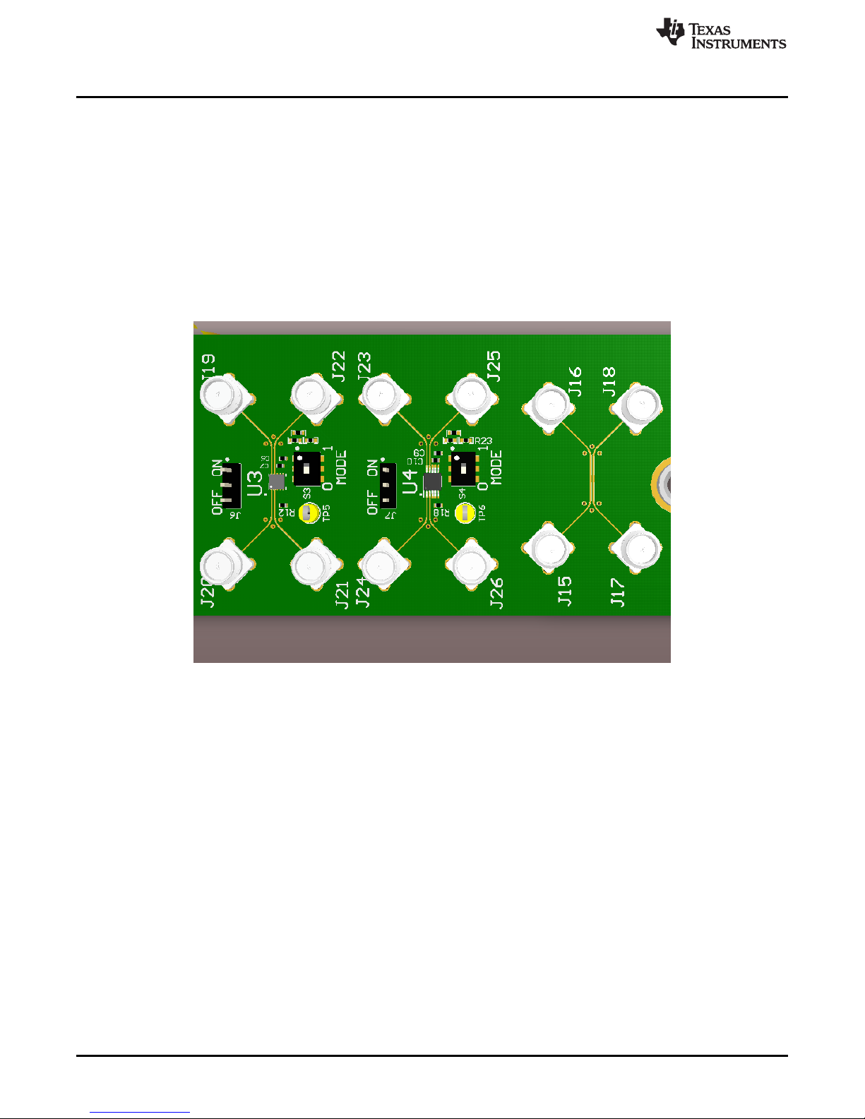
2.3 Bandwidth Evaluation
Devices U3 and U4 are configured to allow for precise bandwidth measurements. The two devices are in a
DSK and DGS package respectively, but otherwise are functionally identical. Each device has SMA
connectors on both the connector and system side of the USB 2.0 Data line pins that offer a low
attenuation way to connect a network analyzer and ensure that during typical operation the TPD2S701-Q1
capacitance and inductance do not impede signal speed past where the maximum line signal speed is. In
addition, when U3 and U4 are placed into a fault state the bandwidth can be measured to ensure that the
DC fault voltage is significantly attenuated. See Figure 3.
There is an additional bandwidth setup that is designed for calibration. The board and trace add some
parasitics and bandwidth loss that do not reflect how the TPD2S701-Q1 operates when designed into a
system. This additional pass-through allows for calibration to account for those and get a more accurate
picture of the bandwidth of the TPD2S701-Q1.
www.ti.com
Figure 3. Bandwidth Evaluation Configuration
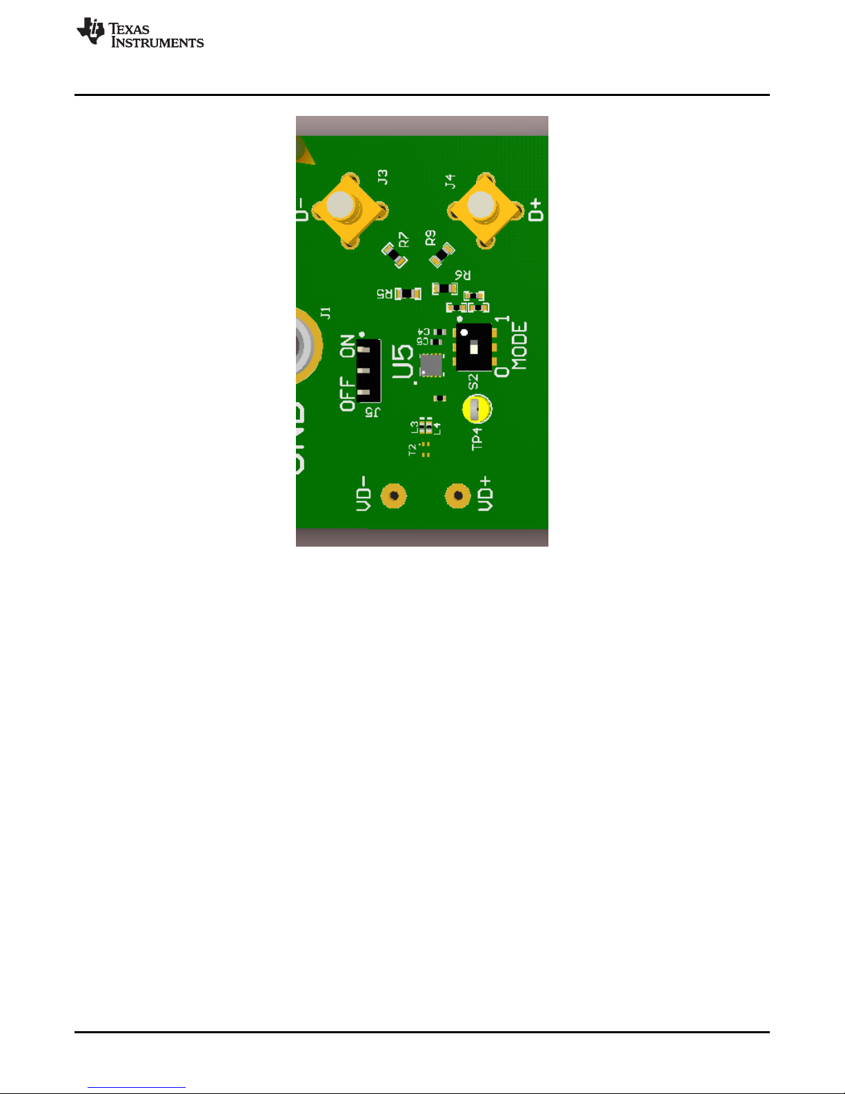
2.4 IEC ESD Evaluation
Device U5 is configured to be an optimal place to test the TPD2S701-Q1 IEC ESD strike response. This
configuration contains the TPD2S701-Q1 in only the DSK package as there is no difference in the
performance between the DSK and DGS packages. Test points VD+ and VD– offer strike points that can
targeted with an external ESD simulator on the protected data lines. By measuring with attenuated scope
probes on the SMB connecters labeled D+ and D– during an ESD strike, the user can capture a waveform
of what the protected system is exposed to during an ESD strike. Resistors R7 and R9 are 150-Ω resistors
in series with the ESD pulse to provide a 4x attenuation with the 50-Ω oscilloscope probe impedance. In
addition to this, to ensure that the oscilloscope is not harmed a 10x attenuation probe must be used. See
Figure 4.
For more information about Texas Instruments recommended ESD test setup, see the application report,
IEC 61000-4-x Tests for TI’s Protection Devices.
4
TPD2S701-Q1 Evaluation Module
Copyright © 2017, Texas Instruments Incorporated
SLVUAU3–January 2017
Submit Documentation Feedback
Page 5
www.ti.com
Board Setup
Figure 4. ESD Evaluation Configuration
SLVUAU3–January 2017
Submit Documentation Feedback
Copyright © 2017, Texas Instruments Incorporated
TPD2S701-Q1 Evaluation Module
5
Page 6

Schematics
3 Schematics
www.ti.com
Figure 5. Schematic Page 1
Figure 6. Schematic Page 2
6
TPD2S701-Q1 Evaluation Module
Figure 7. Schematic Page 3
Copyright © 2017, Texas Instruments Incorporated
SLVUAU3–January 2017
Submit Documentation Feedback
Page 7

www.ti.com
4 Layout
The TPD2S701-Q1 EVM is a 4 layer board of FR4 with measurements of 7.92 inches by 1.9 inches with a
thickness of 62 mil. Only the top and bottom layers are shown below, as the middle two layers are both
ground planes.
Layout
Figure 8. TPD2S701-Q1 Top Layer
Figure 9. TPD2S701-Q1 Bottom Layer
SLVUAU3–January 2017
Submit Documentation Feedback
Copyright © 2017, Texas Instruments Incorporated
TPD2S701-Q1 Evaluation Module
7
Page 8

Bill of Materials
www.ti.com
8
SLVUAU3–January 2017
Submit Documentation Feedback
Copyright © 2017, Texas Instruments Incorporated
TPD2S701-Q1 Evaluation Module
5 Bill of Materials
(1)
Unless otherwise noted in the Alternate PartNumber and/or Alternate Manufacturer columns, all parts may be substituted with equivalents.
Table 1. Bill of Materials
Designator Quantity Value Description Package
Reference
Part
Number
Manufacturer Alternate
PartNumber
(1)
Alternate
Manufacturer
PCB 1 Printed Circuit Board HVL147 Any — —
C1, C8,
C13
3 1 uF CAP, CERM, 1 µF, 100 V, ±10%, X7R,
AEC-Q200 Grade 1, 1206_190
1206_190 GCM31CR72A105K
A03
MuRata
C2, C3,
C4, C5,
C6, C7,
C9, C10,
C11, C12
10 1 uF CAP, CERM, 1 µF, 10 V,±10%, X7S,
AEC-Q200 Grade 1, 0402
0402 GCM155C71A105KE
38D
MuRata
J1 1 Standard Banana Jack, Uninsulated, 5.5mmKeystone_575-4 575-4 Keystone
J2, J5, J6,
J7, J8
5 Header, 100 mil, 3×1, Tin, TH Header, 3 PIN,
100 mil, Tin
PEC03SAAN Sullins Connector
Solutions
J3, J4 2 Connector, SMB,Vertical RCP 0-4 GHz,
50 Ω, TH
236×293×236mil 131-3701-261 Emerson Network Power
J9, J11,
J13
3 Connector, USB Type A, 4POS R/A,
SMD
USB Type A right
angle
0480371000 Molex
J10, J12,
J14
3 Connector,Receptacle, USB TYPE A,
4POS SMD
USB TYPE A
CONNECTOR
RECEPTACLE
4POS SMD
896-43-004-00-
000000
Mill-Max
J15, J16,
J17, J18,
J19, J20,
J21, J22,
J23, J24,
J25, J26
12 SMA Straight PCB Socket Die Cast, 50
Ω, TH
SMA Straight
PCB Socket Die
Cast, TH
5-1814832-1 TE Connectivity
L1, L2, L3,
L4, L5, L6,
L7, L8
8 10 nH Inductor, Multilayer, Air Core, 10 nH,
0.3A, 0.26 Ω, SMD
0402 polarized LQG15HS10NJ02D MuRata
LBL1 1 Thermal Transfer Printable Labels,
1.250" W × 0.250" H - 10,000 per roll
PCB Label 1.25
× 0.250 inch
THT-13-457-10 Brady
R1, R8,
R11, R17,
R19
5 0 RES, 0, 5%, 0.063 W, 0402 0402 RC0402JR-070RL Yageo America
R2, R10,
R12, R18,
R20
5 10k RES, 10 k, 5%, 0.063 W, 0402 0402 CRCW040210K0JN
ED
Vishay-Dale
Page 9

www.ti.com
Bill of Materials
9
SLVUAU3–January 2017
Submit Documentation Feedback
Copyright © 2017, Texas Instruments Incorporated
TPD2S701-Q1 Evaluation Module
Table 1. Bill of Materials (continued)
Designator Quantity Value Description Package
Reference
Part
Number
Manufacturer Alternate
PartNumber
(1)
Alternate
Manufacturer
R3, R13,
R14, R21,
R22
5 140k RES, 140 k, 1%, 0.1 W, AEC-Q200
Grade 0, 0402
0402 ERJ-2RKF1403X Panasonic
R4, R15,
R16, R23,
R24
5 24.9k RES, 24.9 k, 1%, 0.063 W, 0402 0402 CRCW040224K9FK
ED
Vishay-Dale
R5, R6 2 45.3 RES, 45.3, 1%, 0.1 W, 0603 0603 CRCW060345R3FK
EA
Vishay-Dale
R7, R9 2 150 RES, 150, 1%, 0.1 W, 0603 0603 RC0603FR-07150RL Yageo America
S1, S2, S3,
S4, S5
5 SLIDE SWITCH DPDT .1A, SMT SWITCH,
5.4×2.5×3.9 mm
CAS-220TA Copal Electronics
SH-J2, SH-
J5, SH-J6,
SH-J7, SH-
J8
5 Shunt, 2.54 mm, Gold, Black Shunt, 2.54 mm,
Black
60900213421 Wurth Elektronik
T1, T2, T3,
T4
4 SMT Common Mode Choke mcf12102g900 Taiyo Yuden None None
TP1, TP4,
TP5, TP6,
TP7
5 Test Point, Compact, Yellow, TH Yellow Compact
Testpoint
5009 Keystone
TP2 1 Test Point, Compact, Red, TH Red Compact
Testpoint
5005 Keystone
TP3 1 Orange Test Point, Compact, Orange, TH Orange Compact
Testpoint
5008 Keystone
U1, U3, U5 3 Automotive USB 2-Ch Date Line Short-
to-Battery, Short-to-VBUS, and IEC
ESD pritection, DSK0010A
DSK0010A TPD2S701QDSKRQ1Texas Instruments Texas Instruments
U2, U4 2 Automotive USB 2-Ch Date Line Short-
to-Battery, Short-to-VBUS, and IEC
ESD pritection, DGS0010A
DGS0010A TPD2S701QDGSRQ1Texas Instruments Texas Instruments
FID1, FID2,
FID3
0 Fiducial mark. There is nothing to buy or
mount
Fiducial N/A N/A
Page 10

10
SLVUAU3–January 2017
Submit Documentation Feedback
TPD2S701-Q1 Evaluation Module
IMPORTANT NOTICE FOR TI DESIGN INFORMATION AND RESOURCES
Page 11

www.ti.com
Texas Instruments Incorporated (‘TI”) technical, application or other design advice, services or information, including, but not limited to,
reference designs and materials relating to evaluation modules, (collectively, “TI Resources”) are intended to assist designers who are
developing applications that incorporate TI products; by downloading, accessing or using any particular TI Resource in any way, you
(individually or, if you are acting on behalf of a company, your company) agree to use it solely for this purpose and subject to the terms of
this Notice.
TI’s provision of TI Resources does not expand or otherwise alter TI’s applicable published warranties or warranty disclaimers for TI
products, and no additional obligations or liabilities arise from TI providing such TI Resources. TI reserves the right to make corrections,
enhancements, improvements and other changes to its TI Resources.
You understand and agree that you remain responsible for using your independent analysis, evaluation and judgment in designing your
applications and that you have full and exclusive responsibility to assure the safety of your applications and compliance of your applications
(and of all TI products used in or for your applications) with all applicable regulations, laws and other applicable requirements. You
represent that, with respect to your applications, you have all the necessary expertise to create and implement safeguards that (1)
anticipate dangerous consequences of failures, (2) monitor failures and their consequences, and (3) lessen the likelihood of failures that
might cause harm and take appropriate actions. You agree that prior to using or distributing any applications that include TI products, you
will thoroughly test such applications and the functionality of such TI products as used in such applications. TI has not conducted any
testing other than that specifically described in the published documentation for a particular TI Resource.
You are authorized to use, copy and modify any individual TI Resource only in connection with the development of applications that include
the TI product(s) identified in such TI Resource. NO OTHER LICENSE, EXPRESS OR IMPLIED, BY ESTOPPEL OR OTHERWISE TO
ANY OTHER TI INTELLECTUAL PROPERTY RIGHT, AND NO LICENSE TO ANY TECHNOLOGY OR INTELLECTUAL PROPERTY
RIGHT OF TI OR ANY THIRD PARTY IS GRANTED HEREIN, including but not limited to any patent right, copyright, mask work right, or
other intellectual property right relating to any combination, machine, or process in which TI products or services are used. Information
regarding or referencing third-party products or services does not constitute a license to use such products or services, or a warranty or
endorsement thereof. Use of TI Resources may require a license from a third party under the patents or other intellectual property of the
third party, or a license from TI under the patents or other intellectual property of TI.
TI RESOURCES ARE PROVIDED “AS IS” AND WITH ALL FAULTS. TI DISCLAIMS ALL OTHER WARRANTIES OR
REPRESENTATIONS, EXPRESS OR IMPLIED, REGARDING TI RESOURCES OR USE THEREOF, INCLUDING BUT NOT LIMITED TO
ACCURACY OR COMPLETENESS, TITLE, ANY EPIDEMIC FAILURE WARRANTY AND ANY IMPLIED WARRANTIES OF
MERCHANTABILITY, FITNESS FOR A PARTICULAR PURPOSE, AND NON-INFRINGEMENT OF ANY THIRD PARTY INTELLECTUAL
PROPERTY RIGHTS.
TI SHALL NOT BE LIABLE FOR AND SHALL NOT DEFEND OR INDEMNIFY YOU AGAINST ANY CLAIM, INCLUDING BUT NOT
LIMITED TO ANY INFRINGEMENT CLAIM THAT RELATES TO OR IS BASED ON ANY COMBINATION OF PRODUCTS EVEN IF
DESCRIBED IN TI RESOURCES OR OTHERWISE. IN NO EVENT SHALL TI BE LIABLE FOR ANY ACTUAL, DIRECT, SPECIAL,
COLLATERAL, INDIRECT, PUNITIVE, INCIDENTAL, CONSEQUENTIAL OR EXEMPLARY DAMAGES IN CONNECTION WITH OR
ARISING OUT OF TI RESOURCES OR USE THEREOF, AND REGARDLESS OF WHETHER TI HAS BEEN ADVISED OF THE
POSSIBILITY OF SUCH DAMAGES.
You agree to fully indemnify TI and its representatives against any damages, costs, losses, and/or liabilities arising out of your noncompliance with the terms and provisions of this Notice.
This Notice applies to TI Resources. Additional terms apply to the use and purchase of certain types of materials, TI products and services.
These include; without limitation, TI’s standard terms for semiconductor products http://www.ti.com/sc/docs/stdterms.htm), evaluation
modules, and samples (http://www.ti.com/sc/docs/sampterms.htm).
Bill of Materials
Mailing Address: Texas Instruments, Post Office Box 655303, Dallas, Texas 75265
SLVUAU3–January 2017
Submit Documentation Feedback
Copyright © 2017, Texas Instruments Incorporated
Copyright © 2017, Texas Instruments Incorporated
TPD2S701-Q1 Evaluation Module
11
Page 12

STANDARD TERMS FOR EVALUATION MODULES
1. Delivery: TI delivers TI evaluation boards, kits, or modules, including any accompanying demonstration software, components, and/or
documentation which may be provided together or separately (collectively, an “EVM” or “EVMs”) to the User (“User”) in accordance
with the terms set forth herein. User's acceptance of the EVM is expressly subject to the following terms.
1.1 EVMs are intended solely for product or software developers for use in a research and development setting to facilitate feasibility
evaluation, experimentation, or scientific analysis of TI semiconductors products. EVMs have no direct function and are not
finished products. EVMs shall not be directly or indirectly assembled as a part or subassembly in any finished product. For
clarification, any software or software tools provided with the EVM (“Software”) shall not be subject to the terms and conditions
set forth herein but rather shall be subject to the applicable terms that accompany such Software
1.2 EVMs are not intended for consumer or household use. EVMs may not be sold, sublicensed, leased, rented, loaned, assigned,
or otherwise distributed for commercial purposes by Users, in whole or in part, or used in any finished product or production
system.
2 Limited Warranty and Related Remedies/Disclaimers:
2.1 These terms do not apply to Software. The warranty, if any, for Software is covered in the applicable Software License
Agreement.
2.2 TI warrants that the TI EVM will conform to TI's published specifications for ninety (90) days after the date TI delivers such EVM
to User. Notwithstanding the foregoing, TI shall not be liable for a nonconforming EVM if (a) the nonconformity was caused by
neglect, misuse or mistreatment by an entity other than TI, including improper installation or testing, or for any EVMs that have
been altered or modified in any way by an entity other than TI, (b) the nonconformity resulted from User's design, specifications
or instructions for such EVMs or improper sytem design, or (c) User has not paid on time. Testing and other quality control
techniques are used to the extent TI deems necessary. TI does not test all parameters of each EVM.
User's claims against TI under this Section 2 are void if User fails to notify TI of any apparent defects in the EVMs within ten (10)
business days after delivery, or of any hidden defects with ten (10) business days after the defect has been detected.
2.3 TI's sole liability shall be at its option to repair or replace EVMs that fail to conform to the warranty set forth above, or credit
User's account for such EVM. TI's liability under this warranty shall be limited to EVMs that are returned during the warranty
period to the address designated by TI and that are determined by TI not to conform to such warranty. If TI elects to repair or
replace such EVM, TI shall have a reasonable time to repair such EVM or provide replacements. Repaired EVMs shall be
warranted for the remainder of the original warranty period. Replaced EVMs shall be warranted for a new full ninety (90) day
warranty period.
3 Regulatory Notices:
3.1 United States
3.1.1 Notice applicable to EVMs not FCC-Approved:
FCC NOTICE: This kit is designed to allow product developers to evaluate electronic components, circuitry, or software
associated with the kit to determine whether to incorporate such items in a finished product and software developers to write
software applications for use with the end product. This kit is not a finished product and when assembled may not be resold or
otherwise marketed unless all required FCC equipment authorizations are first obtained. Operation is subject to the condition
that this product not cause harmful interference to licensed radio stations and that this product accept harmful interference.
Unless the assembled kit is designed to operate under part 15, part 18 or part 95 of this chapter, the operator of the kit must
operate under the authority of an FCC license holder or must secure an experimental authorization under part 5 of this chapter.
3.1.2 For EVMs annotated as FCC – FEDERAL COMMUNICATIONS COMMISSION Part 15 Compliant:
CAUTION
This device complies with part 15 of the FCC Rules. Operation is subject to the following two conditions: (1) This device may not
cause harmful interference, and (2) this device must accept any interference received, including interference that may cause
undesired operation.
Changes or modifications not expressly approved by the party responsible for compliance could void the user's authority to
operate the equipment.
FCC Interference Statement for Class A EVM devices
NOTE: This equipment has been tested and found to comply with the limits for a Class A digital device, pursuant to part 15 of
the FCC Rules. These limits are designed to provide reasonable protection against harmful interference when the equipment is
operated in a commercial environment. This equipment generates, uses, and can radiate radio frequency energy and, if not
installed and used in accordance with the instruction manual, may cause harmful interference to radio communications.
Operation of this equipment in a residential area is likely to cause harmful interference in which case the user will be required to
correct the interference at his own expense.
Page 13

FCC Interference Statement for Class B EVM devices
NOTE: This equipment has been tested and found to comply with the limits for a Class B digital device, pursuant to part 15 of
the FCC Rules. These limits are designed to provide reasonable protection against harmful interference in a residential
installation. This equipment generates, uses and can radiate radio frequency energy and, if not installed and used in accordance
with the instructions, may cause harmful interference to radio communications. However, there is no guarantee that interference
will not occur in a particular installation. If this equipment does cause harmful interference to radio or television reception, which
can be determined by turning the equipment off and on, the user is encouraged to try to correct the interference by one or more
of the following measures:
• Reorient or relocate the receiving antenna.
• Increase the separation between the equipment and receiver.
• Connect the equipment into an outlet on a circuit different from that to which the receiver is connected.
• Consult the dealer or an experienced radio/TV technician for help.
3.2 Canada
3.2.1 For EVMs issued with an Industry Canada Certificate of Conformance to RSS-210
Concerning EVMs Including Radio Transmitters:
This device complies with Industry Canada license-exempt RSS standard(s). Operation is subject to the following two conditions:
(1) this device may not cause interference, and (2) this device must accept any interference, including interference that may
cause undesired operation of the device.
Concernant les EVMs avec appareils radio:
Le présent appareil est conforme aux CNR d'Industrie Canada applicables aux appareils radio exempts de licence. L'exploitation
est autorisée aux deux conditions suivantes: (1) l'appareil ne doit pas produire de brouillage, et (2) l'utilisateur de l'appareil doit
accepter tout brouillage radioélectrique subi, même si le brouillage est susceptible d'en compromettre le fonctionnement.
Concerning EVMs Including Detachable Antennas:
Under Industry Canada regulations, this radio transmitter may only operate using an antenna of a type and maximum (or lesser)
gain approved for the transmitter by Industry Canada. To reduce potential radio interference to other users, the antenna type
and its gain should be so chosen that the equivalent isotropically radiated power (e.i.r.p.) is not more than that necessary for
successful communication. This radio transmitter has been approved by Industry Canada to operate with the antenna types
listed in the user guide with the maximum permissible gain and required antenna impedance for each antenna type indicated.
Antenna types not included in this list, having a gain greater than the maximum gain indicated for that type, are strictly prohibited
for use with this device.
Concernant les EVMs avec antennes détachables
Conformément à la réglementation d'Industrie Canada, le présent émetteur radio peut fonctionner avec une antenne d'un type et
d'un gain maximal (ou inférieur) approuvé pour l'émetteur par Industrie Canada. Dans le but de réduire les risques de brouillage
radioélectrique à l'intention des autres utilisateurs, il faut choisir le type d'antenne et son gain de sorte que la puissance isotrope
rayonnée équivalente (p.i.r.e.) ne dépasse pas l'intensité nécessaire à l'établissement d'une communication satisfaisante. Le
présent émetteur radio a été approuvé par Industrie Canada pour fonctionner avec les types d'antenne énumérés dans le
manuel d’usage et ayant un gain admissible maximal et l'impédance requise pour chaque type d'antenne. Les types d'antenne
non inclus dans cette liste, ou dont le gain est supérieur au gain maximal indiqué, sont strictement interdits pour l'exploitation de
l'émetteur
3.3 Japan
3.3.1 Notice for EVMs delivered in Japan: Please see http://www.tij.co.jp/lsds/ti_ja/general/eStore/notice_01.page 日本国内に
輸入される評価用キット、ボードについては、次のところをご覧ください。
http://www.tij.co.jp/lsds/ti_ja/general/eStore/notice_01.page
3.3.2 Notice for Users of EVMs Considered “Radio Frequency Products” in Japan: EVMs entering Japan may not be certified
by TI as conforming to Technical Regulations of Radio Law of Japan.
If User uses EVMs in Japan, not certified to Technical Regulations of Radio Law of Japan, User is required to follow the
instructions set forth by Radio Law of Japan, which includes, but is not limited to, the instructions below with respect to EVMs
(which for the avoidance of doubt are stated strictly for convenience and should be verified by User):
1. Use EVMs in a shielded room or any other test facility as defined in the notification #173 issued by Ministry of Internal
Affairs and Communications on March 28, 2006, based on Sub-section 1.1 of Article 6 of the Ministry’s Rule for
Enforcement of Radio Law of Japan,
2. Use EVMs only after User obtains the license of Test Radio Station as provided in Radio Law of Japan with respect to
EVMs, or
3. Use of EVMs only after User obtains the Technical Regulations Conformity Certification as provided in Radio Law of Japan
with respect to EVMs. Also, do not transfer EVMs, unless User gives the same notice above to the transferee. Please note
that if User does not follow the instructions above, User will be subject to penalties of Radio Law of Japan.
Page 14

【無線電波を送信する製品の開発キットをお使いになる際の注意事項】 開発キットの中には技術基準適合証明を受けて
いないものがあります。 技術適合証明を受けていないもののご使用に際しては、電波法遵守のため、以下のいずれかの
措置を取っていただく必要がありますのでご注意ください。
1. 電波法施行規則第6条第1項第1号に基づく平成18年3月28日総務省告示第173号で定められた電波暗室等の試験設備でご使用
いただく。
2. 実験局の免許を取得後ご使用いただく。
3. 技術基準適合証明を取得後ご使用いただく。
なお、本製品は、上記の「ご使用にあたっての注意」を譲渡先、移転先に通知しない限り、譲渡、移転できないものとします。
上記を遵守頂けない場合は、電波法の罰則が適用される可能性があることをご留意ください。 日本テキサス・イ
ンスツルメンツ株式会社
東京都新宿区西新宿6丁目24番1号
西新宿三井ビル
3.3.3 Notice for EVMs for Power Line Communication: Please see http://www.tij.co.jp/lsds/ti_ja/general/eStore/notice_02.page
電力線搬送波通信についての開発キットをお使いになる際の注意事項については、次のところをご覧ください。http:/
/www.tij.co.jp/lsds/ti_ja/general/eStore/notice_02.page
4 EVM Use Restrictions and Warnings:
4.1 EVMS ARE NOT FOR USE IN FUNCTIONAL SAFETY AND/OR SAFETY CRITICAL EVALUATIONS, INCLUDING BUT NOT
LIMITED TO EVALUATIONS OF LIFE SUPPORT APPLICATIONS.
4.2 User must read and apply the user guide and other available documentation provided by TI regarding the EVM prior to handling
or using the EVM, including without limitation any warning or restriction notices. The notices contain important safety information
related to, for example, temperatures and voltages.
4.3 Safety-Related Warnings and Restrictions:
4.3.1 User shall operate the EVM within TI’s recommended specifications and environmental considerations stated in the user
guide, other available documentation provided by TI, and any other applicable requirements and employ reasonable and
customary safeguards. Exceeding the specified performance ratings and specifications (including but not limited to input
and output voltage, current, power, and environmental ranges) for the EVM may cause personal injury or death, or
property damage. If there are questions concerning performance ratings and specifications, User should contact a TI
field representative prior to connecting interface electronics including input power and intended loads. Any loads applied
outside of the specified output range may also result in unintended and/or inaccurate operation and/or possible
permanent damage to the EVM and/or interface electronics. Please consult the EVM user guide prior to connecting any
load to the EVM output. If there is uncertainty as to the load specification, please contact a TI field representative.
During normal operation, even with the inputs and outputs kept within the specified allowable ranges, some circuit
components may have elevated case temperatures. These components include but are not limited to linear regulators,
switching transistors, pass transistors, current sense resistors, and heat sinks, which can be identified using the
information in the associated documentation. When working with the EVM, please be aware that the EVM may become
very warm.
4.3.2 EVMs are intended solely for use by technically qualified, professional electronics experts who are familiar with the
dangers and application risks associated with handling electrical mechanical components, systems, and subsystems.
User assumes all responsibility and liability for proper and safe handling and use of the EVM by User or its employees,
affiliates, contractors or designees. User assumes all responsibility and liability to ensure that any interfaces (electronic
and/or mechanical) between the EVM and any human body are designed with suitable isolation and means to safely
limit accessible leakage currents to minimize the risk of electrical shock hazard. User assumes all responsibility and
liability for any improper or unsafe handling or use of the EVM by User or its employees, affiliates, contractors or
designees.
4.4 User assumes all responsibility and liability to determine whether the EVM is subject to any applicable international, federal,
state, or local laws and regulations related to User’s handling and use of the EVM and, if applicable, User assumes all
responsibility and liability for compliance in all respects with such laws and regulations. User assumes all responsibility and
liability for proper disposal and recycling of the EVM consistent with all applicable international, federal, state, and local
requirements.
5. Accuracy of Information: To the extent TI provides information on the availability and function of EVMs, TI attempts to be as accurate
as possible. However, TI does not warrant the accuracy of EVM descriptions, EVM availability or other information on its websites as
accurate, complete, reliable, current, or error-free.
Page 15

6. Disclaimers:
6.1 EXCEPT AS SET FORTH ABOVE, EVMS AND ANY MATERIALS PROVIDED WITH THE EVM (INCLUDING, BUT NOT
LIMITED TO, REFERENCE DESIGNS AND THE DESIGN OF THE EVM ITSELF) ARE PROVIDED "AS IS" AND "WITH ALL
FAULTS." TI DISCLAIMS ALL OTHER WARRANTIES, EXPRESS OR IMPLIED, REGARDING SUCH ITEMS, INCLUDING BUT
NOT LIMITED TO ANY EPIDEMIC FAILURE WARRANTY OR IMPLIED WARRANTIES OF MERCHANTABILITY OR FITNESS
FOR A PARTICULAR PURPOSE OR NON-INFRINGEMENT OF ANY THIRD PARTY PATENTS, COPYRIGHTS, TRADE
SECRETS OR OTHER INTELLECTUAL PROPERTY RIGHTS.
6.2 EXCEPT FOR THE LIMITED RIGHT TO USE THE EVM SET FORTH HEREIN, NOTHING IN THESE TERMS SHALL BE
CONSTRUED AS GRANTING OR CONFERRING ANY RIGHTS BY LICENSE, PATENT, OR ANY OTHER INDUSTRIAL OR
INTELLECTUAL PROPERTY RIGHT OF TI, ITS SUPPLIERS/LICENSORS OR ANY OTHER THIRD PARTY, TO USE THE
EVM IN ANY FINISHED END-USER OR READY-TO-USE FINAL PRODUCT, OR FOR ANY INVENTION, DISCOVERY OR
IMPROVEMENT, REGARDLESS OF WHEN MADE, CONCEIVED OR ACQUIRED.
7. USER'S INDEMNITY OBLIGATIONS AND REPRESENTATIONS. USER WILL DEFEND, INDEMNIFY AND HOLD TI, ITS
LICENSORS AND THEIR REPRESENTATIVES HARMLESS FROM AND AGAINST ANY AND ALL CLAIMS, DAMAGES, LOSSES,
EXPENSES, COSTS AND LIABILITIES (COLLECTIVELY, "CLAIMS") ARISING OUT OF OR IN CONNECTION WITH ANY
HANDLING OR USE OF THE EVM THAT IS NOT IN ACCORDANCE WITH THESE TERMS. THIS OBLIGATION SHALL APPLY
WHETHER CLAIMS ARISE UNDER STATUTE, REGULATION, OR THE LAW OF TORT, CONTRACT OR ANY OTHER LEGAL
THEORY, AND EVEN IF THE EVM FAILS TO PERFORM AS DESCRIBED OR EXPECTED.
8. Limitations on Damages and Liability:
8.1 General Limitations. IN NO EVENT SHALL TI BE LIABLE FOR ANY SPECIAL, COLLATERAL, INDIRECT, PUNITIVE,
INCIDENTAL, CONSEQUENTIAL, OR EXEMPLARY DAMAGES IN CONNECTION WITH OR ARISING OUT OF THESE
TERMS OR THE USE OF THE EVMS , REGARDLESS OF WHETHER TI HAS BEEN ADVISED OF THE POSSIBILITY OF
SUCH DAMAGES. EXCLUDED DAMAGES INCLUDE, BUT ARE NOT LIMITED TO, COST OF REMOVAL OR
REINSTALLATION, ANCILLARY COSTS TO THE PROCUREMENT OF SUBSTITUTE GOODS OR SERVICES, RETESTING,
OUTSIDE COMPUTER TIME, LABOR COSTS, LOSS OF GOODWILL, LOSS OF PROFITS, LOSS OF SAVINGS, LOSS OF
USE, LOSS OF DATA, OR BUSINESS INTERRUPTION. NO CLAIM, SUIT OR ACTION SHALL BE BROUGHT AGAINST TI
MORE THAN TWELVE (12) MONTHS AFTER THE EVENT THAT GAVE RISE TO THE CAUSE OF ACTION HAS
OCCURRED.
8.2 Specific Limitations. IN NO EVENT SHALL TI'S AGGREGATE LIABILITY FROM ANY USE OF AN EVM PROVIDED
HEREUNDER, INCLUDING FROM ANY WARRANTY, INDEMITY OR OTHER OBLIGATION ARISING OUT OF OR IN
CONNECTION WITH THESE TERMS, , EXCEED THE TOTAL AMOUNT PAID TO TI BY USER FOR THE PARTICULAR
EVM(S) AT ISSUE DURING THE PRIOR TWELVE (12) MONTHS WITH RESPECT TO WHICH LOSSES OR DAMAGES ARE
CLAIMED. THE EXISTENCE OF MORE THAN ONE CLAIM SHALL NOT ENLARGE OR EXTEND THIS LIMIT.
9. Return Policy. Except as otherwise provided, TI does not offer any refunds, returns, or exchanges. Furthermore, no return of EVM(s)
will be accepted if the package has been opened and no return of the EVM(s) will be accepted if they are damaged or otherwise not in
a resalable condition. If User feels it has been incorrectly charged for the EVM(s) it ordered or that delivery violates the applicable
order, User should contact TI. All refunds will be made in full within thirty (30) working days from the return of the components(s),
excluding any postage or packaging costs.
10. Governing Law: These terms and conditions shall be governed by and interpreted in accordance with the laws of the State of Texas,
without reference to conflict-of-laws principles. User agrees that non-exclusive jurisdiction for any dispute arising out of or relating to
these terms and conditions lies within courts located in the State of Texas and consents to venue in Dallas County, Texas.
Notwithstanding the foregoing, any judgment may be enforced in any United States or foreign court, and TI may seek injunctive relief
in any United States or foreign court.
Mailing Address: Texas Instruments, Post Office Box 655303, Dallas, Texas 75265
Copyright © 2017, Texas Instruments Incorporated
Page 16

IMPORTANT NOTICE FOR TI DESIGN INFORMATION AND RESOURCES
Texas Instruments Incorporated (‘TI”) technical, application or other design advice, services or information, including, but not limited to,
reference designs and materials relating to evaluation modules, (collectively, “TI Resources”) are intended to assist designers who are
developing applications that incorporate TI products; by downloading, accessing or using any particular TI Resource in any way, you
(individually or, if you are acting on behalf of a company, your company) agree to use it solely for this purpose and subject to the terms of
this Notice.
TI’s provision of TI Resources does not expand or otherwise alter TI’s applicable published warranties or warranty disclaimers for TI
products, and no additional obligations or liabilities arise from TI providing such TI Resources. TI reserves the right to make corrections,
enhancements, improvements and other changes to its TI Resources.
You understand and agree that you remain responsible for using your independent analysis, evaluation and judgment in designing your
applications and that you have full and exclusive responsibility to assure the safety of your applications and compliance of your applications
(and of all TI products used in or for your applications) with all applicable regulations, laws and other applicable requirements. You
represent that, with respect to your applications, you have all the necessary expertise to create and implement safeguards that (1)
anticipate dangerous consequences of failures, (2) monitor failures and their consequences, and (3) lessen the likelihood of failures that
might cause harm and take appropriate actions. You agree that prior to using or distributing any applications that include TI products, you
will thoroughly test such applications and the functionality of such TI products as used in such applications. TI has not conducted any
testing other than that specifically described in the published documentation for a particular TI Resource.
You are authorized to use, copy and modify any individual TI Resource only in connection with the development of applications that include
the TI product(s) identified in such TI Resource. NO OTHER LICENSE, EXPRESS OR IMPLIED, BY ESTOPPEL OR OTHERWISE TO
ANY OTHER TI INTELLECTUAL PROPERTY RIGHT, AND NO LICENSE TO ANY TECHNOLOGY OR INTELLECTUAL PROPERTY
RIGHT OF TI OR ANY THIRD PARTY IS GRANTED HEREIN, including but not limited to any patent right, copyright, mask work right, or
other intellectual property right relating to any combination, machine, or process in which TI products or services are used. Information
regarding or referencing third-party products or services does not constitute a license to use such products or services, or a warranty or
endorsement thereof. Use of TI Resources may require a license from a third party under the patents or other intellectual property of the
third party, or a license from TI under the patents or other intellectual property of TI.
TI RESOURCES ARE PROVIDED “AS IS” AND WITH ALL FAULTS. TI DISCLAIMS ALL OTHER WARRANTIES OR
REPRESENTATIONS, EXPRESS OR IMPLIED, REGARDING TI RESOURCES OR USE THEREOF, INCLUDING BUT NOT LIMITED TO
ACCURACY OR COMPLETENESS, TITLE, ANY EPIDEMIC FAILURE WARRANTY AND ANY IMPLIED WARRANTIES OF
MERCHANTABILITY, FITNESS FOR A PARTICULAR PURPOSE, AND NON-INFRINGEMENT OF ANY THIRD PARTY INTELLECTUAL
PROPERTY RIGHTS.
TI SHALL NOT BE LIABLE FOR AND SHALL NOT DEFEND OR INDEMNIFY YOU AGAINST ANY CLAIM, INCLUDING BUT NOT
LIMITED TO ANY INFRINGEMENT CLAIM THAT RELATES TO OR IS BASED ON ANY COMBINATION OF PRODUCTS EVEN IF
DESCRIBED IN TI RESOURCES OR OTHERWISE. IN NO EVENT SHALL TI BE LIABLE FOR ANY ACTUAL, DIRECT, SPECIAL,
COLLATERAL, INDIRECT, PUNITIVE, INCIDENTAL, CONSEQUENTIAL OR EXEMPLARY DAMAGES IN CONNECTION WITH OR
ARISING OUT OF TI RESOURCES OR USE THEREOF, AND REGARDLESS OF WHETHER TI HAS BEEN ADVISED OF THE
POSSIBILITY OF SUCH DAMAGES.
You agree to fully indemnify TI and its representatives against any damages, costs, losses, and/or liabilities arising out of your noncompliance with the terms and provisions of this Notice.
This Notice applies to TI Resources. Additional terms apply to the use and purchase of certain types of materials, TI products and services.
These include; without limitation, TI’s standard terms for semiconductor products http://www.ti.com/sc/docs/stdterms.htm), evaluation
modules, and samples (http://www.ti.com/sc/docs/sampterms.htm).
Mailing Address: Texas Instruments, Post Office Box 655303, Dallas, Texas 75265
Copyright © 2017, Texas Instruments Incorporated
 Loading...