

Page 1

Safety Manual for TMS570LC4x Hercules ARM Safety MCUs
User's Guide
Literature Number: SPNU540A
May 2014–Revised September 2016
Page 2

Contents
1 Introduction ........................................................................................................................ 8
2 Hercules TMS570LC4x Product Overview.............................................................................. 10
2.1 Targeted Applications .................................................................................................. 11
2.2 Product Safety Constraints ............................................................................................ 12
3 Hercules Development Process for Management of Systematic Faults ..................................... 13
3.1 TI Standard MCU Automotive Development Process ............................................................. 14
3.2 TI MCU Automotive Legacy IEC 61508 Development Process.................................................. 15
3.3 Yogitech fRMethodology Development Process ................................................................... 15
3.4 Hercules Enhanced Safety Development Process................................................................. 15
4 Hercules Product Architecture for Management of Random Faults........................................... 18
4.1 Safe Island Philosophy and Architecture Partition to Support Safety Analysis (FMEA/FMEDA) ............ 18
4.2 Identification of Parts/Elements....................................................................................... 19
4.3 Management of Family Variants...................................................................................... 20
4.4 Operating States........................................................................................................ 20
4.5 Management of Errors ................................................................................................. 22
5 System Integrator Recommendations ................................................................................... 23
5.1 System Integrator Activities ........................................................................................... 23
5.2 Hints for Performing Dependent/Common Cause Failure Analysis Including the Hercules MCU ........... 25
5.3 Hints for Improving Independence of Function/Co-Existence of Function When Using the Hercules MCU 25
5.4 Support for System Integrator Activities ............................................................................. 25
6 Brief Description of Elements .............................................................................................. 26
6.1 Power Supply ........................................................................................................... 26
6.2 Power Management Module (PMM) ................................................................................. 26
6.3 Clocks.................................................................................................................... 27
6.4 Reset ..................................................................................................................... 27
6.5 System Control Module................................................................................................ 28
6.6 Error Signaling Module (ESM) ....................................................................................... 29
6.7 CPU Subsystem ........................................................................................................ 29
6.8 Primary Embedded Flash ............................................................................................. 31
6.9 Flash EEPROM Emulation (FEE) .................................................................................... 32
6.10 Primary Embedded SRAM ............................................................................................ 33
6.11 CPU Interconnect Subsystem......................................................................................... 34
6.12 Peripheral Interconnect Subsystem .................................................................................. 35
6.13 Peripheral Central Resource 1 (PCR1).............................................................................. 35
6.14 Peripheral Central Resource 2 (PCR2).............................................................................. 36
6.15 Peripheral Central Resource 3 (PCR3).............................................................................. 36
6.16 EFuse Static Configuration ............................................................................................ 37
6.17 OTP Static Configuration.............................................................................................. 37
6.18 I/O Multiplexing Module (IOMM)...................................................................................... 38
6.19 Vectored Interrupt Module (VIM) ..................................................................................... 38
6.20 Real Time Interrupt (RTI).............................................................................................. 39
2
Table of Contents
Copyright © 2014–2016, Texas Instruments Incorporated
SPNU540A–May 2014–Revised September 2016
Submit Documentation Feedback
Page 3

www.ti.com
6.21 Direct Memory Access (DMA) ........................................................................................ 40
6.22 High-End Timer (N2HET), HET Transfer Unit (HTU) .............................................................. 40
6.23 Multi-Buffered Analog-to-Digital Converter (MibADC) ............................................................. 42
6.24 Enhanced Pulse Width Modulators (ePWM)........................................................................ 42
6.25 Enhanced Capture (eCAP)............................................................................................ 43
6.26 Enhanced Quadrature Encoder Pulse (eQEP) ..................................................................... 44
6.27 Multi Buffered Serial Peripheral Interface (MibSPI)................................................................ 44
6.28 Inter-Integrated Circuit (I2C) .......................................................................................... 45
6.29 Serial Communication Interface (SCI) ............................................................................... 46
6.30 Local Interconnect Network (LIN) .................................................................................... 46
6.31 Controller Area Network (DCAN)..................................................................................... 47
6.32 FlexRay, FlexRay Transfer Unit (FTU) .............................................................................. 48
6.33 General-Purpose Input/Output (GIO) ................................................................................ 49
6.34 Ethernet.................................................................................................................. 50
6.35 External Memory Interface (EMIF) ................................................................................... 50
6.36 JTAG Debug, Trace, Calibration, and Test Access................................................................ 51
6.37 Cortex-R5F Central Processing Unit (CPU) Debug and Trace................................................... 51
6.38 Data Modification Module (DMM)..................................................................................... 52
6.39 RAM Trace Port Interface (RTP) ..................................................................................... 52
6.40 Parameter Overlay Module (POM)................................................................................... 52
6.41 Error Profiling Controller (EPC)....................................................................................... 53
6.42 Temperature Sensor ................................................................................................... 53
7 Brief Description of Diagnostics........................................................................................... 54
7.1 1oo2 Software Voting Using Secondary Free Running Counter ................................................. 54
7.2 Bit Error Detection ...................................................................................................... 54
7.3 Bit Multiplexing in FEE Memory Array ............................................................................... 54
7.4 Bit Multiplexing in Flash Memory Array.............................................................................. 54
7.5 Bit Multiplexing in Primary SRAM Memory Array................................................................... 54
7.6 Bit Multiplexing in Peripheral SRAM Memory Array................................................................ 54
7.7 CPU Illegal Operation and Instruction Trapping ................................................................... 55
7.8 Logic Built In Self-Test (LBIST) ...................................................................................... 55
7.9 Logic Built In Self-Test (LBIST) Auto-Coverage.................................................................... 56
7.10 CPU Lockstep Compare .............................................................................................. 56
7.11 VIM Lockstep Compare ............................................................................................... 56
7.12 Lockstep Comparator Self-Test....................................................................................... 56
7.13 CPU Online Profiling Using the Performance Monitoring Unit.................................................... 56
7.14 CPU Memory Protection Unit (MPU)................................................................................. 57
7.15 CRC Auto-coverage.................................................................................................... 57
7.16 CRC in Message........................................................................................................ 57
7.17 DCAN Acknowledge Error Detection................................................................................. 57
7.18 DCAN Form Error Detection .......................................................................................... 57
7.19 DCAN Stuff Error Detection........................................................................................... 57
7.20 DCAN Protocol CRC in Message..................................................................................... 57
7.21 Disable the DMM Pin Interface ....................................................................................... 58
7.22 Disable the RTP Pin Interface ........................................................................................ 58
7.23 Dual Clock Comparator (DCC)........................................................................................ 58
7.24 Autoload Self-Test...................................................................................................... 58
7.25 Efuse Autoload Self-Test Auto-Coverage ........................................................................... 58
7.26 EFuse ECC.............................................................................................................. 58
SPNU540A–May 2014–Revised September 2016
Submit Documentation Feedback
Copyright © 2014–2016, Texas Instruments Incorporated
Contents
3
Page 4

www.ti.com
7.27 EFuse ECC Logic Self-Test........................................................................................... 58
7.28 eQEP Quadrature Watchdog.......................................................................................... 58
7.29 eQEP Software Test of Quadrature Watchdog Functionality ..................................................... 59
7.30 Error Trapping - IOMM................................................................................................. 59
7.31 Error Trapping (including Peripheral Slave Error Trapping) - L2/L3 Interconnect.............................. 59
7.32 Ethernet Alignment Error Detection.................................................................................. 59
7.33 Ethernet Physical Layer Fault ........................................................................................ 59
7.34 External Monitoring of Warm Reset (nRST) ........................................................................ 59
7.35 External Monitoring via ECLK......................................................................................... 59
7.36 External Voltage Supervisor........................................................................................... 60
7.37 External Watchdog ..................................................................................................... 60
7.38 FEE Contents Check by Hardware CRC ............................................................................ 60
7.39 FEE Data ECC.......................................................................................................... 60
7.40 FEE Sector Protection ................................................................................................. 60
7.41 Flash Address and Control Bus Parity............................................................................... 61
7.42 Flash Contents Check by Hardware CRC........................................................................... 61
7.43 Flash ECC ............................................................................................................... 61
7.44 Flash Hard Error Cache and Livelock................................................................................ 61
7.45 Flash Sector Protection ................................................................................................ 62
7.46 Flash Wrapper Address ECC ......................................................................................... 62
7.47 Flash Wrapper Diag Mode 5 Test .................................................................................... 62
7.48 Flash Wrapper Diag Mode 7 Test .................................................................................... 62
7.49 FlexRay 1oo2 Voting Using Both FlexRay Channels .............................................................. 62
7.50 FlexRay CCF Clock Correction Failure Detection.................................................................. 62
7.51 FlexRay EDA / EDB Error Detection................................................................................. 62
7.52 FlexRay FIFO Overrun Detection..................................................................................... 62
7.53 FlexRay Message Handler Error Detection ......................................................................... 63
7.54 FlexRay Sync Frames Below Minimum / Sync Frame Overflow ................................................. 63
7.55 FlexRay Transmission Across Boundary Error Detection......................................................... 63
7.56 Glitch Filtering on nRST and nPORRST ............................................................................ 63
7.57 Hardware CRC Check of External Memory ......................................................................... 63
7.58 Hardware CRC Check of OTP Contents ............................................................................ 63
7.59 Hardware Disable of JTAG Port ...................................................................................... 63
7.60 Information Redundancy Techniques ................................................................................ 63
7.61 Information Redundancy Techniques - CPU Specific ............................................................. 64
7.62 Information Redundancy Techniques - DCAN Specific............................................................ 64
7.63 Information Redundancy Techniques - DMA Specific ............................................................. 64
7.64 Information Redundancy Techniques Including End-to-End Safing - FlexRay Specific....................... 64
7.65 Information Redundancy Techniques - N2HET Specific .......................................................... 64
7.66 Internal Voltage Monitor (VMON) .................................................................................... 65
7.67 Internal Watchdog ...................................................................................................... 65
7.68 IOMM Master ID Filtering.............................................................................................. 65
7.69 LIN Checksum Error Detection ....................................................................................... 65
7.70 LIN No-Response Error Detection.................................................................................... 65
7.71 LIN Physical Bus Error Detection..................................................................................... 66
7.72 LIN / SCI Bit Error Detection .......................................................................................... 66
7.73 LIN / SCI Frame Error Detection ..................................................................................... 66
7.74 LIN / SCI Overrun Error Detection.................................................................................... 66
4
Contents
Copyright © 2014–2016, Texas Instruments Incorporated
SPNU540A–May 2014–Revised September 2016
Submit Documentation Feedback
Page 5

www.ti.com
7.75 Locking Mechanism for Control Registers........................................................................... 66
7.76 Lockout of JTAG Access Using AJSM............................................................................... 66
7.77 Low Power Oscillator Clock Detector (LPOCLKDET).............................................................. 66
7.78 Memory Protection Unit (MPU) for Non-CPU Bus Masters ...................................................... 66
7.79 MibADC Calibration .................................................................................................... 67
7.80 MibADC Information Redundancy Techniques..................................................................... 67
7.81 MibADC Input Self-Test................................................................................................ 67
7.82 MibSPI/SPI Data Length Error Detection............................................................................ 67
7.83 MibSPI/SPI Data Overrun Detection................................................................................. 67
7.84 MibSPI/SPI Slave Desync Detection................................................................................. 67
7.85 MibSPI/SPI Slave Timeout Detection................................................................................ 67
7.86 Monitoring by Second N2HET ........................................................................................ 68
7.87 Monitoring by eCAP or N2HET ....................................................................................... 68
7.88 Non-Privileged Bus Master Access .................................................................................. 68
7.89 OTP Autoload ECC..................................................................................................... 68
7.90 Parity in Message....................................................................................................... 68
7.91 Periodic Hardware CRC Check of OTP Contents.................................................................. 68
7.92 PCR Access Management: Protection Mode and MasterID Filtering............................................ 68
7.93 Periodic Hardware CRC Check of SRAM Contents................................................................ 69
7.94 Periodic Software Read Back of Static Configuration Registers ................................................ 69
7.95 Peripheral SRAM Parity................................................................................................ 69
7.96 Peripheral Memory ECC............................................................................................... 69
7.97 PLL Slip Detector ....................................................................................................... 69
7.98 Primary SRAM Address and Control Bus Parity.................................................................... 69
7.99 Primary SRAM Data and ECC Storage in Multiple Physical Banks per Logical Address..................... 70
7.100 Primary SRAM Correctable ECC Profiling .......................................................................... 70
7.101 ECC on Cache RAM................................................................................................... 70
7.102 Primary SRAM Data ECC............................................................................................. 70
7.103 Primary SRAM Wrapper Redundant Address Decode............................................................ 70
7.104 Primary SRAM Hard Error Cache and Livelock .................................................................... 71
7.105 Privileged Mode Access and Multi-Bit Enable Keys for Control Registers ..................................... 71
7.106 PBIST Check of Primary or Module SRAM ......................................................................... 71
7.107 PBIST Auto-coverage.................................................................................................. 72
7.108 Power Domain Inactivity Monitor..................................................................................... 72
7.109 PBIST Test of Parity Bit Memory..................................................................................... 72
7.110 PBIST Test of ECC Bit Memory...................................................................................... 72
7.111 Lockstep PSCON....................................................................................................... 72
7.112 Redundant Address Decode Self-Test .............................................................................. 72
7.113 Redundant Temperature Sensors.................................................................................... 72
7.114 Scrubbing of SRAM to Correct Detected Single Bit Errors ....................................................... 72
7.115 Shadow Registers...................................................................................................... 73
7.116 Software Check of Cause of Last Reset ........................................................................... 73
7.117 Software Read Back of CPU Registers ............................................................................. 73
7.118 Software Read Back of Written Configuration...................................................................... 73
7.119 Software Test of DCC Functionality ................................................................................. 73
7.120 Software Test of DWD Functionality................................................................................. 73
7.121 Software Test of DWWD Functionality .............................................................................. 73
7.122 Software Test of ECC Profiler (EPC) ................................................................................ 73
7.123 Software Test of Error Path Reporting .............................................................................. 73
SPNU540A–May 2014–Revised September 2016
Submit Documentation Feedback
Copyright © 2014–2016, Texas Instruments Incorporated
Contents
5
Page 6

www.ti.com
7.124 Software Test of Flash Sector Protection Logic.................................................................... 73
7.125 Software Test of Function Including Error Tests ................................................................... 74
7.126 Software Test of Function Using I/O Loopback .................................................................... 74
7.127 Software Test of Function Using I/O Checking In GIO Mode .................................................... 74
7.128 Software Test of Function Using I/O Loopback in Transceiver/PHY ........................................... 74
7.129 Software Test of Function Using I/O Loopback in Transceiver / PHY - FlexRay .............................. 74
7.130 Software Test of Function Using I/O Loopback Including Error Tests - IOMM Only .......................... 74
7.131 Software Test of Hardware CRC..................................................................................... 75
7.132 Software Test of MPU Functionality ................................................................................. 75
7.133 Software Test of Parity Logic ......................................................................................... 75
7.134 Software Test of PBIST ............................................................................................... 75
7.135 Software Test of SRAM Wrapper Address Decode Diagnostic and ECC ...................................... 75
7.136 Software Test for Reset ............................................................................................... 75
7.137 Software Warm Reset Generation................................................................................... 75
7.138 Transmission Redundancy............................................................................................ 75
7.139 Use of CoreSight Debug Logic Key Enable Scheme.............................................................. 75
7.140 Use of DCC as Program Sequence Watchdog..................................................................... 76
7.141 Use of MPUs to Block Access to Memory Mapped Debug....................................................... 76
7.142 Execution of Interconnect Self-Test.................................................................................. 76
7.143 CPU Interconnect Hardware Checker............................................................................... 76
7.144 Timeout Monitoring on The Bus Transaction ....................................................................... 76
7.145 Transaction ECC (Data Lines) ....................................................................................... 76
7.146 Transaction Parity (Address and Control Lines) ................................................................... 77
7.147 Peripheral Interconnect New Memory Protection Unit (NMPU) .................................................. 77
7.148 Software Test of The New Memory Protection Unit (NMPU) Functionality..................................... 77
7.149 Software Test of ECC Logic .......................................................................................... 77
7.150 Multi-Bit Keyed Self-Correctable High-Integrity Bits ............................................................... 77
8 Next Steps in Your Safety Development ................................................................................ 78
Appendix A Summary of Safety Feature Usage.............................................................................. 79
Appendix B Development Interface Agreement ............................................................................ 130
B.1 Appointment of Safety Managers.................................................................................. 130
B.2 Tailoring of the Safety Lifecycle.................................................................................... 130
B.3 Activities Performed by TI .......................................................................................... 132
B.4 Information to be Exchanged....................................................................................... 133
B.5 Parties Responsible for Safety Activities ......................................................................... 133
B.6 Communication of Target Values.................................................................................. 134
B.7 Supporting Processes and Tools.................................................................................. 134
B.8 Supplier Hazard and Risk Assessment........................................................................... 134
B.9 Creation of Functional Safety Concept ........................................................................... 134
Appendix C Revision History ..................................................................................................... 135
6
Contents
Copyright © 2014–2016, Texas Instruments Incorporated
SPNU540A–May 2014–Revised September 2016
Submit Documentation Feedback
Page 7

www.ti.com
1 Device Revision Code Identification....................................................................................... 9
2 Hercules Product Architecture Overview................................................................................ 10
3 TI Standard MCU Automotive QM Development Process............................................................ 14
4 Hercules Enhanced Functional Safety Development Process....................................................... 17
5 Partition of Hercules MCU for Safety Analysis ......................................................................... 18
6 Operating States of the Hercules MCU ................................................................................. 21
7 Lockstep Temporal Diversity.............................................................................................. 30
8 Hercules Tailoring of Safety Lifecycle.................................................................................. 131
1 Identification of Parts/Elements .......................................................................................... 19
2 Summary of ESM Error Indication ....................................................................................... 22
3 Key to Summary of Safety Features and Diagnostics................................................................. 79
4 Summary of Safety Features and Diagnostics ........................................................................ 80
5 Activities Performed by TI vs. Performed by SEooC Customer .................................................... 132
6 Product Safety Documentation.......................................................................................... 133
7 Product Functional Documentation to be Considered in Safety-Related Design................................. 133
8 Product Safety Documentation Tools and Formats.................................................................. 134
9 SPNU540A Revisions.................................................................................................... 135
List of Figures
List of Tables
SPNU540A–May 2014–Revised September 2016
Submit Documentation Feedback
Copyright © 2014–2016, Texas Instruments Incorporated
List of Figures
7
Page 8

User's Guide
SPNU540A–May 2014–Revised September 2016
Safety Manual for TMS570LC4x Hercules ARM Safety
MCUs
1 Introduction
You, a system and equipment manufacturer or designer, are responsible to ensure that your systems (and
any TI hardware or software components incorporated in your systems) meet all applicable safety,
regulatory, and system-level performance requirements. All application and safety related information in
this document (including application descriptions, suggested safety measures, suggested TI products, and
other materials) is provided for reference only. You understand and agree that your use of TI components
in safety critical applications is entirely at your risk, and that you (as buyer) agree to defend, indemnify,
and hold harmless TI from any and all damages, claims, suits, or expense resulting from such use.
This document is a safety manual for the Texas Instruments Hercules safety critical microcontroller
product family. The product family utilizes a common safety architecture that is implemented in multiple
application focused products. Product configurations supported by this safety manual include silicon
revisions A and B of the following products: (Note that the part numbers listed below are for revision B;
other revisions are slightly different. The device revision can be determined by the symbols marked on the
top of the device as seen in Figure 1 below this list).
• TMS570LS Safety Critical Microcontrollers
– TMS570LC4357-ZWT (Orderable Part #: TMS5704357BZWTQQ1)
– TMS570LC4357-ZWT (Orderable Part #: TMS5704357BZWTQQ1R)
– TMS570LC4355-ZWT (Orderable Part #: TMS5704355BZWTQQ1)
– TMS570LC4355-ZWT (Orderable Part #: TMS5704355BZWTQQ1R)
– TMS570LC4355-ZWT (Orderable Part #: TMS5704355BZWTSQ1)
– TMS570LC4355-ZWT (Orderable Part #: TMS5704355BZWTSQ1R)
– TMS570LC4343-ZWT (Orderable Part #: TMS5704343BZWTQQ1)
– TMS570LC4343-ZWT (Orderable Part #: TMS5704343BZWTQQ1R)
– TMS570LC4343-ZWT (Orderable Part #: TMS5704343BZWTSQ1)
– TMS570LC4343-ZWT (Orderable Part #: TMS5704343BZWTSQ1R)
SafeTI is a trademark of Texas Instruments.
ARM, Cortex are registered trademarks of ARM Limited.
Adobe is a trademark of Adobe Systems Incorporated in the United States, and/or other countries.
IBM, DOORS are registered trademarks of International Business Machines Corporation, registered in many jurisdictions worldwide.
Microsoft, Excel are registered trademarks of Microsoft Corporation in the United States and/or other countries, or both.
All other trademarks are the property of their respective owners.
8
Safety Manual for TMS570LC4x Hercules ARM Safety MCUs
Copyright © 2014–2016, Texas Instruments Incorporated
SPNU540A–May 2014–Revised September 2016
Submit Documentation Feedback
Page 9
4357BZWTQQ1
##B - #######
TMS570LC
G1
__
Device Revision Code
www.ti.com
This Safety Manual provides information needed by system developers to assist in the creation of a safety
critical system using a supported Hercules microcontroller. This document contains:
• An overview of the superset product architecture
• An overview of the development process utilized to reduce systematic failures
• An overview of the safety architecture for management of random failures
• The details of architecture partitions, implemented safety mechanisms
The following information is documented in the Safety Analysis Report Summary for TMS570LC4x ARM®Based Safety Critical Microcontrollers (SPNU541) and is not repeated in this document:
• Summary of failure rates of the MCU estimated at the chip level
• Assumptions of use utilized in calculation of safety metrics
• Summary of targeted standard (IEC 61508, ISO 26262, and so forth) safety metrics at the chip level
The following information is documented in the Detailed Safety Analysis Report for TMS570LC4x ARM®Based Safety Critical Microcontrollers (SPNU542) and is not repeated in this document:
• Fault model used to estimate device failure rates suitable to enable calculation of customized failure
• Quantitative FMEA (also known as FMEDA, Failure Modes, Effects, and Diagnostics Analysis) with
The following information is documented in the Safety Report, and will not be repeated in this document:
• Results of assessments of compliance to targeted standards
The user of this document should have a general familiarity with the Hercules product families. For more
information, see http://www.ti.com/hercules. This document is intended to be used in conjunction with the
pertinent data sheets, technical reference manuals, and other documentation for the products under
development.
For information which is beyond the scope of the listed deliverables, please contact your TI sales
representative or http://www.ti.com.
Introduction
Figure 1. Device Revision Code Identification
rates
detail to the sub-module level of the device, suitable to enable calculation based on customized
application of diagnostics
SPNU540A–May 2014–Revised September 2016
Submit Documentation Feedback
Safety Manual for TMS570LC4x Hercules ARM Safety MCUs
Copyright © 2014–2016, Texas Instruments Incorporated
9
Page 10
Level Two Hierarchy
Level Three Hierarchy
Level One Hierarchy
Cortex R5F CPU
Cluster
Bus Master
Peripheral
Bus Master
Peripheral
Debug Bus
Master
General
DMA
Level Two
CPU Master
Level Two
CPU Slave
Peripheral Central Resource 1
Peripheral
Peripheral
Peripheral
Peripheral
Peripheral
Peripheral
Bus Master
Peripheral
Peripheral Central Resource n
Peripheral
Peripheral
Peripheral
Peripheral
Peripheral
Peripheral
Low Latency
Peripheral Port
Peripheral InterconnectCPU Interconnect
CRCCRC
Flash External
Memory
Interface
SRAM
Flash Emulated
EEPROM
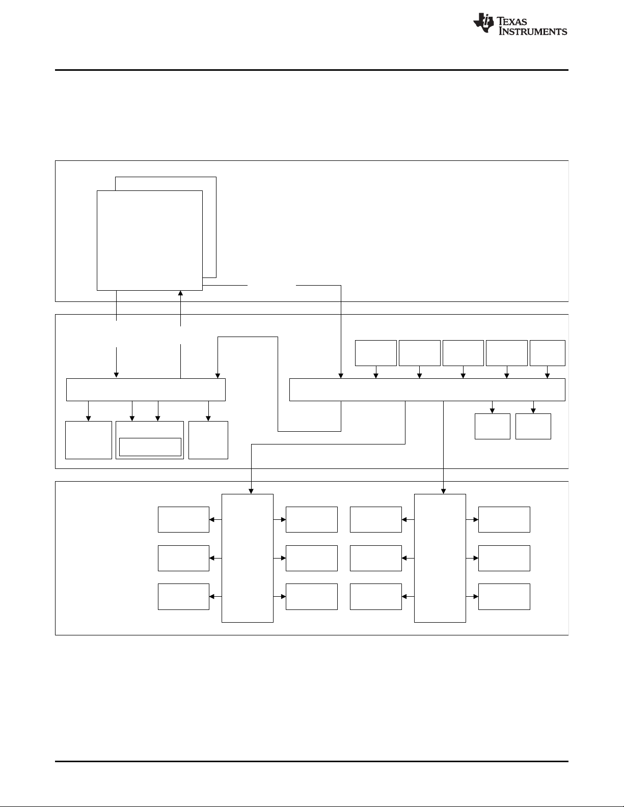
Hercules TMS570LC4x Product Overview
2 Hercules TMS570LC4x Product Overview
The TMS570LC4x 65 nm Hercules product family is an evolution of the proven TMS570LS Hercules
products in the 65 nm manufacturing process. A simplified graphical view of the product superset
architecture can be seen in Figure 2. This is a basic representation of the architecture and is not all
inclusive. For example, products in the family may scale based on the number of peripherals, number of
bus master peripherals, or amount of memory - but the programmer's model remains consistent.
www.ti.com
Figure 2. Hercules Product Architecture Overview
10
Safety Manual for TMS570LC4x Hercules ARM Safety MCUs
Copyright © 2014–2016, Texas Instruments Incorporated
SPNU540A–May 2014–Revised September 2016
Submit Documentation Feedback
Page 11

www.ti.com
The Hercules product architecture utilizes the ARM Cortex®-R5F CPU in a cached memory configuration
with both instruction and data caches. The Cortex-R5F CPU is implemented with a checker Cortex-R5F
CPU in a lockstep configuration. This provides cycle by cycle checking of correct CPU operation while
keeping a simple, easy to use, single core programmer's model. The Cortex R5F CPU has a multithreaded level two bus master interface, which provides access to the level two memory hierarchy,
supporting up to seven concurrent CPU accesses in flight. A level two slave interface allows bus masters
access to the level one cache memories for test, debug, and fault insertion purposes. A separate low
latency peripheral port provides access to peripherals. In addition, a Snoop Control Unit (SCU) module is
present to snoop non-CPU bus master accesses for the purpose of I/O cache coherency.
The level two device hierarchy is dominated by two switched central resource interconnect modules (also
known as bus matrices or crossbars): CPU Interconnect Subsystem and Peripheral Interconnect
Subsystem. These device level interconnect modules allow multiple bus masters to access multiple bus
slaves. Prioritization, routing, decode, and arbitration functions are provided. Access to the memory
subsystem (Flash, FEE, SRAM, and EMIF) is provided via the CPU Interconnect Subsystem. Peripherals
are accessed via the Peripheral Interconnect Subsystem and multiple level three peripheral interconnect
segments (PCR1, PCR2, and PCR3). Bus masters to the level two device hierarchy include CPUs, bus
master peripherals, debug bus masters, and general purpose direct memory access (DMA) controllers.
Bus slaves on the level two hierarchy include the primary Flash memory, primary SRAM, Flash EEPROM
emulation memory, and external memory interface (EMIF), one or more peripheral bus segments (PCRs),
and Cortex-R5F slave port access..
The level three hierarchy is primarily composed of peripherals. Peripherals are grouped into one or more
peripheral bus segments (PCRs), managed by a peripheral central resource. The peripheral central
resource provides address decode functionality for bus transactions targeting peripherals.
Hercules TMS570LC4x Product Overview
2.1 Targeted Applications
The Hercules MCU family is targeted at general purpose safety applications. Multiple safety applications
were analyzed during the concept phase in order to support Safety Element out of Context (SEooC)
development according to ISO 26262-10:2012. Example target applications include:
• Automotive braking systems, including anti-lock braking (ABS), anti-lock braking with traction control
(ABS+ TC), and electronic stability control (ESC)
• Motor control systems, particularly electronic power steering (EPS) systems and electric vehicle (EV)
power train
• General purpose safety computation, such as integrated sensor cluster processing and vehicle strategy
generation in an active safety system
• Industrial automation such as programmable logic controllers (PLCs) and programmable automation
controllers (PACs) for safety critical process control
In the case of overlapping requirements between target systems, TI has attempted to design the device
respecting the most stringent requirements. For example, the fault tolerant time intervals for timer logic in
an ESC application are typically on the order of 100 ms. In an EPS application, the fault tolerant time
interval is typically on the order of 10 ms. In such case, TI has performed timer subsystem analysis
respecting <10 ms fault tolerant time interval.
While TI considered certain applications during the development of these devices, this should not restrict a
customer who wishes to implement other systems. With all safety critical components, rationalization of
the component safety concept to the system safety concept should be executed by the system integrator.
SPNU540A–May 2014–Revised September 2016
Submit Documentation Feedback
Copyright © 2014–2016, Texas Instruments Incorporated
Safety Manual for TMS570LC4x Hercules ARM Safety MCUs
11
Page 12

Hercules TMS570LC4x Product Overview
2.2 Product Safety Constraints
This device is a Type B device, as defined in IEC 61508:2010
This device claims no hardware fault tolerance (HFT = 0), as defined in IEC 61508:2010
For safety components developed according to many safety standards, it is expected that the component
safety manual will provide a list of product safety constraints. For a simple component, or more complex
components developed for a single application, this is a reasonable response. However, the Hercules
product family is both a complex design and is not developed targeting a single, specific application.
Therefore, a single set of product safety constraints cannot govern all viable uses of the product. The
Detailed Safety Analysis Report for TM570LC4x ARM®-Based Safety Critical Microcontrollers (SPNU542)
provides a reference implementation of the Hercules product in a common system with relevant product
safety constraints.
www.ti.com
12
Safety Manual for TMS570LC4x Hercules ARM Safety MCUs
Copyright © 2014–2016, Texas Instruments Incorporated
SPNU540A–May 2014–Revised September 2016
Submit Documentation Feedback
Page 13

www.ti.com
Hercules Development Process for Management of Systematic Faults
3 Hercules Development Process for Management of Systematic Faults
For a safety critical development, it is necessary to manage both systematic and random faults. Texas
Instruments has created a unique development process for safety critical semiconductors that greatly
reduces probability of systematic failure. This process builds on a standard Quality Managed (QM)
development process as the foundation for safety critical development. This process is then augmented by
a second layer of development activities that are specific to safety critical developments targeting IEC
61508 and ISO 26262.
In 2007, TI first saw the need to augment this standard development process in order to develop products
according to IEC 61508. TI engaged with safety industry leader exida consulting to ensure the
development was compliant to the standard. During 2008, a process for safety critical development
according to IEC 61508 1st edition was implemented. This process has been executed on multiple
microcontroller developments that are currently shipping into safety critical systems. The Hercules family
product and safety architectures described in this document began development under the IEC 61508
development flow.
By mid 2009, it became clear that the emerging IEC 61508 2nd edition and ISO 26262 functional safety
standards would require enhanced process flow capabilities. Due to the lack of maturity of these draft
standards, it was not possible to implement a development process that ensured compliance before final
drafts were available.
TI joined the ISO 26262 working group in mid 2009 as a way to better understand and influence the
standard with respect to microcontroller hardware component development. As part of the US Technical
Advisory Group (TAG) and international working group for ISO 26262, TI has notable contributions to:
• ISO 26262-5;Annex D - informative section describing failure modes and recommended diagnostics for
hardware components, enhanced by TI's detailed knowledge of silicon failure modes and effectiveness
of diagnostic methods
• ISO 26262-10;Clause 9 - informative section describing development of safety elements out of context,
a technique that legitimizes and enables the use of Commercial Off The Shelf (COTS) safety critical
components
• ISO 26262-10;Annex A - informative section describing how to apply ISO 26262 to microcontrollers,
influenced by TI's lessons learned in application of IEC 61508 to microcontroller development
In mid 2010, TI started development of a process flow compliant to IEC 61508 2nd edition and ISO 26262
draft baseline 18. TI worked in detail with Yogitech in the ISO 26262 international working group and
found that the companies have complementary capabilities. A partnership was established for engineering
services and safety consulting services to accelerate new safety-related product development. Yogitech's
existing fRMethodology development process and TI's IEC 61508 development process were merged and
enhanced to create a new process addressing both ISO 26262 and IEC 61508 2nd edition. This process
has gone through a process of continual improvement as ISO 26262 standards development continues.
The process applied to the Hercules silicon covered by this document incorporates all changes through
ISO 26262:2012 international standard release for part 10 and the ISO 26262:2011 international standard
release for parts 1-9.
SPNU540A–May 2014–Revised September 2016
Submit Documentation Feedback
Copyright © 2014–2016, Texas Instruments Incorporated
Safety Manual for TMS570LC4x Hercules ARM Safety MCUs
13
Page 14
Business
Opportunity
Prescreen
Program
Planning
Create
Validate
Sample
Characterize
Qualify
Ramp Æ Sustain
Design In Team
Sustain
Team
Cross Functional Team
Identify new
product
opportunities
Develop
project plan
IC design and
layout
Characterize
Develop
manufacturing
test
Develop & build marketing collateral
Sample to
customers
Qualification
Build initial inventory
Optimize test
flow and yeilds
Manage project risks (market and execution)
Bench & ATE
verification
CP0
Commission
Review
CP1
Design
Kickoff
Review
CP2
PG Review
CP2.5
Qual Start
Review
CP3
TMS Review
CP4 Safe
Launch
Review
Hercules Development Process for Management of Systematic Faults
3.1 TI Standard MCU Automotive Development Process
Texas Instruments has been developing automotive microcontrollers for safety critical and non-safety
critical automotive applications for over twenty years. Automotive markets have strong requirements on
quality management and high reliability of product. Though not explicitly developed for compliance to a
functional safety standard, the TI standard MCU Automotive development process already features many
elements necessary to manage systematic faults. This development process can be considered to be
Quality Managed (QM), but does not achieve an IEC 61058 Safety Integrity Level (SIL) or ISO 26262
Automotive Safety Integrity Level (ASIL). For up-to-date information on TI quality process certifications,
see http://www.ti.com/quality.
The standard process breaks development into phases:
• Business opportunity pre-screen
• Program planning
• Create
• Validate, sample, and characterize
• Qualify
• Ramp to production and sustaining production
The standard process is illustrated in Figure 3.
www.ti.com
Figure 3. TI Standard MCU Automotive QM Development Process
14
Safety Manual for TMS570LC4x Hercules ARM Safety MCUs
Copyright © 2014–2016, Texas Instruments Incorporated
SPNU540A–May 2014–Revised September 2016
Submit Documentation Feedback
Page 15

www.ti.com
Hercules Development Process for Management of Systematic Faults
3.2 TI MCU Automotive Legacy IEC 61508 Development Process
Texas Instruments developed an initial process for developing safety critical automotive microcontrollers in
2008. This process was developed targeting the IEC 61508 1st edition standard, as augmented with
available committee drafts of the 2nd edition. The process is developed as an additional layer of activities
that should be carried out in addition to the standard MCU Automotive QM development process. This
process as applied on the TMS570LS20216S product development has been assessed suitable for use in
IEC 61508 SIL 3 applications by exida Certification S.A. (certificate TI 071227 C001). In July 2012 the
development process and the TMS570LS20x/10x product family was assessed to the IEC 61508:2010
standard and certified suitable for use in IEC 61508 SIL 3 applications by exida Certification Services
(certificate TI 1204073 C001).
Key new activities in this process included:
• Nomination of a safety manager with ownership of all safety related activities
• Development of a safety plan to track safety related activities
• Generation, application, and validation of safety requirements
• Execution of qualitative (FMEA) and quantitative (FMEDA) safety analysis
• Authoring of safety manual and safety analysis report to support customer development
3.3 Yogitech fRMethodology Development Process
fRMethodology is the “white-box” approach for safety design exploration proprietary of YOGITECH,
including:
• fRFMEA, a methodology to perform the FMEA of an integrated circuit in accordance to IEC 61508 and
ISO 26262
• fRFI, a tool to perform fault injection of an integrated circuit based on inputs derived from fRFMEA
YOGITECH’s fRMethodology is in line with ISO 26262-10; Annex A. It mainly consists of:
• Splitting the component or system in elementary parts (“sensitive zones”)
• Computing their failure rates
• Using those failure rates to compute safety metrics
• Validating the results with fault injection
• Allowing sensitivity analyses of those metrics by changing architectural or technological parameters
• Delivering to the customer numbers to compare different architectures
3.4 Hercules Enhanced Safety Development Process
The Hercules enhanced safety development process is a merger of the existing TI and Yogitech flows for
functional safety development. The goal of the process development is to take the best aspects of each
flow and collaborate, resulting in the best in class capabilities to reduce systematic faults.
The process flow is targeted for compliance to IEC 61508 and ISO 26262, and is under a process of
continuous improvement to incorporate new features of emerging functional safety standards. These
functional safety standards are targeted because TI and Yogitech believe they best represent the state of
the art in functional safety development for semiconductors. While not directly targeted at other functional
safety standards, it is expected that products developed to industry state-of-the-art can be readily utilized
in other functional safety systems.
The resulting flow was subsequently assessed by TUEV SUED for compliance to IEC 61508 and ISO
26262 and further enhanced based on technical findings. The development flow is certified by TUEV
SUED under certificate Q4B 13 03 84071 001.
SPNU540A–May 2014–Revised September 2016
Submit Documentation Feedback
Copyright © 2014–2016, Texas Instruments Incorporated
Safety Manual for TMS570LC4x Hercules ARM Safety MCUs
15
Page 16

Hercules Development Process for Management of Systematic Faults
Key elements of the combined process flow are:
• Assumptions on system level design, safety concept, and requirements based on TI's expertise in
safety critical systems development
• Combined qualitative and quantitative or similar safety analysis techniques comprehending the sum of
silicon failure modes and diagnostic techniques known to both TI and Yogitech
• Fault estimation based on multiple industry standards as well as TI manufacturing data
• Application of Yogitech's state-of-the-art fault injection techniques for validation of claimed diagnostic
coverage
• Integration of lessons learned by both companies through multiple safety critical developments to IEC
61508 and participation in the ISO 26262 international working group
The Figure 4 is shown below in a simplified graphic.
www.ti.com
16
Safety Manual for TMS570LC4x Hercules ARM Safety MCUs
Copyright © 2014–2016, Texas Instruments Incorporated
SPNU540A–May 2014–Revised September 2016
Submit Documentation Feedback
Page 17

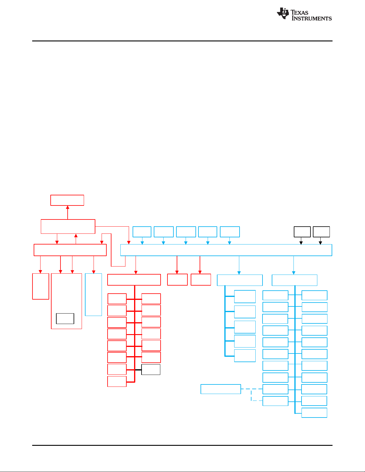
Phase 0
Business
Opportunity
Prescreen
Phase 1
Program Planning
Phase 2
Create
Phase 2.5
Validate, Sample,
and
Characterize
Phase 3
Qualify
Phase 4
Ramp/Sustain
Determine if safety
process execution is
necessary
Execute development
interface agreement
(DIA) with lead
customers and
suppliers
Define SIL/ASIL
capability
Generate safety plan
Initiate safety case
Analyze system to
generate system level
safety assumptions
and requirements
Develop component
level safety
requirements
Validate component
safety requirements
meet system safety
requirements
Implement safety
requirements in design
specification
Validate design
specification meets
component safety
requirements
Confirmation measure
review
Validate safety design
in silicon
Release safety
manual
Release safety
analysis report
Characterization of
safety design
Confirmation measure
review
Qualification of safety
design
Release safety case
report
Update safety manual
(if needed)
Update safety analysis
report (if needed)
Confirmation measure
review
Implement plans to
support operation and
production
Update safety case
report (if needed)
Periodic confirmation
measure reviews
Qualitative analysis of
design (FMEA and
FTA)
Develop safety
product preview
Validation of safety
design at RTL level
Quantitative analysis
of design (FMEDA)
Validation of safety
design at gate/layout
level
Confirmation measure
review
Execute safety design
Incorporate findings
into safety design
Incorporate findings
into safety design
www.ti.com
Hercules Development Process for Management of Systematic Faults
SPNU540A–May 2014–Revised September 2016
Submit Documentation Feedback
Figure 4. Hercules Enhanced Functional Safety Development Process
Copyright © 2014–2016, Texas Instruments Incorporated
Safety Manual for TMS570LC4x Hercules ARM Safety MCUs
17
Page 18
EMIF
PMM
Peripheral Interconnect Subsystem
IOMM
DCAN1
DCAN3
MibSPI1
DCAN4
Peripheral Central
Resource #1
EMIF
Slave
CPU Interconnect Subsystem
Flash
with ECC
&
Flash for
EEPROM
Emulation
with ECC
SRAM
With
ECC
EPC
SCM
CCM-
R5F
MibSPI2
MibSPI3
MibSPI4
MibSPI5
LIN1/SCI1
LIN2/SCI2
SCI3
SCI4
I2C1
I2C2
FlexRay
GIO
N2HET1
N2HET2
MibADC1
MibADC2
EMAC
Slaves
eQEP
1,2
eCAP
1...6
eTPWM
1...7
DCAN2
CRC1
SYS
Dual Cortex-R5F CPUs in
Lockstep
CPU Cache
with ECC
DCC1
Lockstep
VIMs
RTI
STC1
DCC2
STC2
ESM
Peripheral Central
Resource #2
Peripheral Central
Resource #3
HTU2FTUHTU1EMACDMA DMMDAP
CRC2
RTP
POM
EFUSE
Temp Sensor[1...3]
Hercules Product Architecture for Management of Random Faults
4 Hercules Product Architecture for Management of Random Faults
For a safety critical development it is necessary to manage both systematic and random faults. The
Hercules product architecture includes many safety mechanisms, which can detect and respond to
random faults when used correctly. This section of the document describes the architectural safety
concept for the MCU.
4.1 Safe Island Philosophy and Architecture Partition to Support Safety Analysis (FMEA/FMEDA)
The TMS570 Hercules processors share a common safety architecture concept called a “safe island”
philosophy. The basic concept involves a balance between application of hardware diagnostics and
software diagnostics to manage functional safety, while balancing cost concerns. In the “safe island”
approach, a core set of elements are allocated continuously operating hardware safety mechanisms. This
core set of elements, including power and clock and reset, CPU, Flash memory, SRAM and associated
interconnect to Flash and SRAM, is needed to assure any functionally correct execution of software. Once
correct operation of these elements is confirmed, software can be executed on these elements in order to
provide software-based diagnostics on other device elements, such as peripherals. This concept has been
proven viable through multiple generations of safety-critical products in the automotive passenger vehicle
space.
Figure 5 illustrates the safe island approach overlaid to a superset configuration of the Hercules product
architecture.
www.ti.com
18
Figure 5. Partition of Hercules MCU for Safety Analysis
Safety Manual for TMS570LC4x Hercules ARM Safety MCUs
Copyright © 2014–2016, Texas Instruments Incorporated
SPNU540A–May 2014–Revised September 2016
Submit Documentation Feedback
Page 19

www.ti.com
Figure 5 illustrates three architectural partitions:
• “Safe Island Layer” (RED) – This is the region of logic that is needed for all processing operations. This
logic is protected heavily by on board hardware diagnostics and specific assumptions of use to assure
a high level of confidence in safe operation. Once this region is safed, it can be used to provide
comprehensive software diagnostics on other design elements.
• “Blended Layer” (BLUE) – This is the region of logic that includes most safety critical peripherals. This
region has less reliance on hardware diagnostics. Software diagnostics and application protocols are
overlaid to provide the remainder of needed diagnostic coverage.
• “Offline Layer” (BLACK) – This region of logic has minimal or no integrated hardware diagnostics.
Many features in this layer are used only for debug, test, and calibration functions; they are not active
during safety critical operation. Logic in this region could be utilized for safety critical operation
assuming appropriate software diagnostics or system level measures are added by the system
integrator.
4.2 Identification of Parts/Elements
For the purposes of a safety analysis, each module on this device can be considered to be a part or
element. Each part or element has been assigned a three letter unique identifier, which is used uniformly
in the Safety Manual, Safety Analysis Report, and FMEDA Documents to identify the element and it's
diagnostics. Table 1 lists each element present on this device and the unique identifier for this element.
The overall IEC 61508 systematic capability of the MCU is SC3. TI does not make claims of systematic
capability for specific IP modules on the device.
Table 1. Identification of Parts/Elements
Hercules Product Architecture for Management of Random Faults
Part / Element Name Unique Identifier
Clock CLK
Cortex-R5F Central Processing Unit (CPU) CPU
Controller Area Network (DCAN) CAN
Cortex-R5F Central Processing Unit (CPU) Debug and Trace DBG
CPU Interconnect Subsystem MEM
Data Modification Unit DMM
Direct Memory Access (DMA) DMA
Enhanced Capture (eCAP) CAP
EFuse Static Configuration EFU
External Memory Interface (EMIF) EMF
Enhanced Pulse Width Modulators (ePWM) PWM
Enhanced Quadrature Encoder Pulse (eQEP) QEP
Error Profiling Controller EPC
Error Signaling Module (ESM) ESM
Ethernet ETH
Flash EEPROM Emulation (FEE) FEE
Primary Flash FLA
FlexRay Including FlexRay Transfer Unit (FTU) FRY
General Purpose Input/Output (GIO) GIO
Inter-Integrated Circuit (I2C) IIC
Input/Output (I/O) Multiplexing Module (IOMM) IOM
Joint Technical Action Group (JTAG) Debug/Trace/Calibration
Access
Local Interconnect Network (LIN) LIN
Multi-Buffered Analog to Digital Converter (MibADC) ADC
Multi-Buffered Serial Peripheral Interface (MibSPI) MSP
High-End Timer (N2HET) Including HET Transfer Unit (HTU) HET
One Time Programmable (OTP) Flash Static Configuration OTP
JTG
SPNU540A–May 2014–Revised September 2016
Submit Documentation Feedback
Copyright © 2014–2016, Texas Instruments Incorporated
Safety Manual for TMS570LC4x Hercules ARM Safety MCUs
19
Page 20
Hercules Product Architecture for Management of Random Faults
Table 1. Identification of Parts/Elements (continued)
Part / Element Name Unique Identifier
Peripheral Interconnect Subsystem PER
Peripheral Central Resource 1 P1T
Peripheral Central Resource 2 P2T
Peripheral Central Resource 3 P3T
Power Management Module (PMM) PMM
Parameter Overlay Module POM
Power Supply PWR
RAM Trace Port RTP
Reset RST
Real Time Interrupt (RTI) Operating System Timer RTI
Serial Communications Interface (SCI) SCI
SRAM RAM
System Control Module SYS
Temperature Sensors TSN
Vectored Interrupt Module (VIM) VIM
NOTE: The terms "element" and "part" may have specific meaning and imply specific requirements
dependent on the targeted functional safety standard. The terms are used here in a general sense.
TheHercules Architecture Brief Description of Elements section contains a brief description of the
elements listed above. For a full functional description of any of these modules, see the device-specific
technical reference manual.
www.ti.com
4.3 Management of Family Variants
The Hercules family architecture supports multiple product variants. These products could be implemented
as unique silicon designs or they can be shared silicon designs that have elements disabled or not
assured by specification, even if present in silicon. Only the elements of the superset architecture that are
specifically detailed in the device-specific data sheet and technical reference manual are assured to be
present and operate. When developing for the Hercules platform, it is recommended that the safety
concept be based on the superset product architecture to enable maximum scalability across family
variants. The superset architecture shown in the previous section is valid for all device part numbers noted
in the introduction of the safety manual.
4.4 Operating States
The Hercules MCU products have a common architectural definition of operating states. These operating
states should be observed by the system developer in their software and system level design concepts.
The operating states state machine is shown in Figure 6 and described below.
20
Safety Manual for TMS570LC4x Hercules ARM Safety MCUs
Copyright © 2014–2016, Texas Instruments Incorporated
SPNU540A–May 2014–Revised September 2016
Submit Documentation Feedback
Page 21
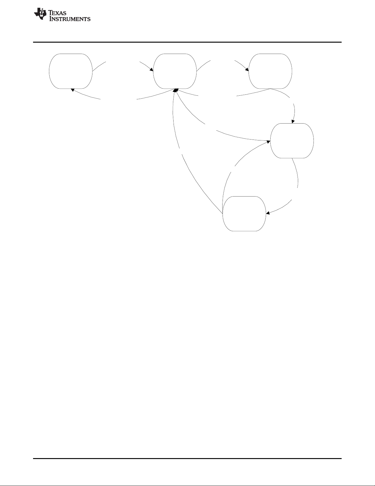
SafePowered Off
Power applied
nPORRST held
Cold Boot
nPORRST released
Warm Boot
SYS_nRST released internally
Operational
Proof tests completed
System init completed
nPORRST driven
Power Removed
SYS_nRST driven
nPORRST driven
nPORRST driven
www.ti.com
Hercules Product Architecture for Management of Random Faults
Figure 6. Operating States of the Hercules MCU
• "Powered Off" - This is the initial operating state of the Hercules MCU. No power is applied to either
core or I/O power supply and the device is non-functional. This state can only transition to the safe
state, and can only be reached from the safe state.
• "Safe" - In the safe state, the Hercules MCU is powered but non-operational. The nPORRST (power-on
reset, also known as cold reset) is asserted by the system but is not released until power supplies
have ramped to a stable state. The internal voltage monitor (VMON) safety mechanism also continues
to assert the nPORRST internal to the device if power supplies are not within a minimum operational
range. When the product is in the safe state, the CPU and peripherals are non-functional. Output
drivers are tri-stated and input/output pins are kept in an input only state.
• "Cold Boot" - In the cold boot state, key analog elements, digital control logic, and debug logic are
initialized for future use. The CPU remains powered but non-operational. When the cold boot process
is completed, the SYS_nRST signal is internally released, leading to the warm boot stage. The
SYS_nRST signal transition change can be monitored externally on the SYS_nRST I/O pin.
• "Warm Boot" - The warm boot mode resets digital logic and enables the CPU. The CPU begins
executing software from Flash memory and software initialization of the device can begin. There is no
hardware interlock to say that warm boot is completed; this is a software decision.
• "Operational" - During the operational mode, the device is capable of supporting safety critical
functionality.
SPNU540A–May 2014–Revised September 2016
Submit Documentation Feedback
Copyright © 2014–2016, Texas Instruments Incorporated
Safety Manual for TMS570LC4x Hercules ARM Safety MCUs
21
Page 22

Hercules Product Architecture for Management of Random Faults
4.5 Management of Errors
When a diagnostic detects a fault, the error must be indicated. The Hercules product architecture provides
aggregation of fault indication from internal safety mechanisms using a peripheral logic known as the error
signaling module (ESM). The ESM provides mechanisms to classify errors by severity and to provide
programmable error response. The ESM does not, in and of itself, impact the overall function of the device
and serves the limited purpose of fault aggregation and classification. The error classifications in the ESM
are summarized in Table 2.
Table 2. Summary of ESM Error Indication
Error Group Interrupt Response Error Pin Response Notes
1
2 Non maskable interrupt generated Error pin activated For errors that are generally of critical severity
3 No interrupt response Error pin activated
The error response is action that is taken by the MCU or system when an error is indicated. There are
multiple potential of error response possible for the Hercules product. The system integrator is responsible
to determine what error response should be taken and to ensure that this is consistent with the system
safety concept.
• CPU abort - This response is implemented directly in the CPU, for diagnostics implemented in the
CPU. During an abort, the program sequence transfers context to an abort handler and software has
an opportunity to manage the fault.
• CPU interrupt - This response can be implemented for diagnostics outside the CPU. An interrupt
allows events external to the CPU to generate a program sequence context transfer to an interrupt
handler where software has an opportunity to manage the fault.
• Generation of SYS_nRST - This response allows the device to change states to warm boot from
operational state. The SYS_nRST could be generated from an external monitor or internally by the
software reset or watchdog. Re-entry to the warm reset state allows possibility for software recovery
when recovery in the operational state was not possible.
• Generation of nPORRST - This response allows the device to change state to safe state from cold
boot, warm boot, or operational states. From this state, it is possible to re-enter cold boot to attempt
recovery when recovery via warm boot is not possible. It is also possible to move to the powered-down
state, if desired, to implement a system level safe state. This response can be generated from the
internal voltage monitor, but is primarily driven by monitors external to the MCU.
The ESM provides multiple registers that can be read by the CPU to determine the current status of
diagnostics and the state of the nERROR pin. For the severe group 2 errors, a shadow register is
provided that is not reset by SYS_nRST. This allows the possibility of warm reset reinitialization to identify
that a group 2 error initiated the external reset.
It is possible for the CPU to trigger the nERROR pin response manually to test system behavior or to
notify external logic of an internal fault not automatically indicated to ESM. The CPU is responsible to clear
indicated errors in the ESM, including clearing of the nERROR pin response.
The EPC is used as a complement to the ESM for error profiling . The primary goal of this module is to
provide a unified correctable ECC error (single bit ECC fault) profiling capability and error address cache
on ECC failures in system bus memory slaves like Flash, FEE, and SRAM. The secondary goal of this
module is to provide an ECC error reporting capability for bus masters, which do not natively have ECC
logic built in like the DMA and TUs. The ECC generation and evaluation logic for bus masters such as
DMA and the TUs are built into the CPU Interconnect Subsystem.
System level management of the external error response can be simplified through the use of a TI
TPS6538x power supply and safety companion device developed for use with the Hercules family.
Programmable interrupt and
programmable interrupt priority
Programmable response
www.ti.com
For errors that are generally not of critical
severity
For critical errors that are seen by diagnostic
implemented in CPU
22
Safety Manual for TMS570LC4x Hercules ARM Safety MCUs
Copyright © 2014–2016, Texas Instruments Incorporated
SPNU540A–May 2014–Revised September 2016
Submit Documentation Feedback
Page 23

www.ti.com
5 System Integrator Recommendations
You, as a system and equipment manufacturer or designer, are responsible to ensure that your systems
(and any TI hardware or software components incorporated in your systems) meet all applicable safety,
regulatory, and system-level performance requirements. All application and safety related information in
this document (including application descriptions, suggested safety measures, suggested TI products, and
other materials) is provided for reference only. You understand and agree that your use of TI components
in safety critical applications is entirely at your risk, and that you (as buyer) agree to defend, indemnify,
and hold TI harmless from any and all damages, claims, suits, or expense resulting from such use.
A brief description of each element on this device and the general assumptions of use are provided in
Section 6.
A list of diagnostic mechanisms for this device and a brief description for each diagnostic are provided in
Section 7.
The effectiveness of the hardware safety mechanisms is noted in the Detailed Safety Analysis Report for
TM570LC4x ARM®-Based Safety Critical Microcontrollers (SPNU542).
This information should be used to determine the strategy for utilizing safety mechanisms. The details of
each safety mechanism can be found in the device-specific technical reference manual.
Depending on the safety standard and end equipment targeted, it may be necessary to manage not only
single point faults, but also latent faults. Per ISO 26262, a latent fault occurs when a fault capable of
violating a safety goal occurs simultaneously to a fault in the diagnostic mechanism that would normally
provide diagnostic coverage for that fault. Latent fault testing does not need to occur during the fault
tolerant time interval, but can be performed at boot time, at shut down, or periodically as determined by
the system developer. Many of the safety mechanisms described in this section can be used as primary
diagnostics, diagnostics for latent fault, or both. When considering system design for management of
latent faults, take care to include failure of execution resources when considering latent faults with
software diagnostics, such as failure of CPU and memories.
System Integrator Recommendations
5.1 System Integrator Activities
The system integrator is responsible for carrying out a number of product development activities. These
activities carried out may include but are not limited to the following:
• Operational and Environmental Constraints
– Verify that the implementation of the TI component in the system design is compliant to
requirements in TI documentation. This includes but is not limited to the requirements found in
technical reference manuals, data sheets, errata documents, safety manuals, and safety analysis
reports
– Verify that the system operational lifetime (power-on hours) does not exceed lifetime specifications
for the TI component, as specified in the device data sheet. If the operational lifetime (power-on
hours) is not specified in the data sheet, the use case does not match published conditions, or
there are questions regarding device lifetime, please contact a TI quality/reliability engineering
representative or http://www.ti.com.
– Define system maintenance requirements. The Hercules MCU does not require maintenance.
– Define system repair requirements. The Hercules MCU is non-repairable with respect to permanent
faults. A power-on reset of the Hercules MCU may be considered a repair activity for transient
faults per some definitions of system repair requirements.
– Define system decommissioning requirements. The Hercules MCU has no specific decommisioning
requirements.
– Define system disposal requirements. The Hercules MCU has no specific disposal requirements.
• Avoidance of Systematic Errors
– Verify the application of appropriate best practices at all stages of hardware and system
development (including development of hardware and system diagnostics external to the MCU) to
avoid systematic failure and to control random failures. This may include but is not limited to
compliance to the requirements documented in IEC61508-2;Annex A Tables A.15 through A.18, as
well as Annex B Tables B.1 through B.6
– Verify that any software implemented (including software diagnostics) is developed with an
SPNU540A–May 2014–Revised September 2016
Submit Documentation Feedback
Copyright © 2014–2016, Texas Instruments Incorporated
Safety Manual for TMS570LC4x Hercules ARM Safety MCUs
23
Page 24

System Integrator Recommendations
appropriate set of measures to avoid systematic errors
• Safety Concept Definition
– Define the supported safety functions and verify that the microcontroller behaves properly to
support execution of the defined safety function. This microcontroller is a generic product, which is
capable of supporting a variety of safety functions but does not have fixed support for any specific
safety function.
– Define the system-level safe state concept considering safe-state entry, maintenance of safe state,
and safe-state exit as appropriate to the application and verify correct implementation
– Define the system-level error-handling concept and verify correct implementation.
– Define appropriate overall timing requirements for safety metrics to be calculated for the application
– Define appropriate safety metric targets for the application
• Safety Concept Implementation
– Select and implement an appropriate set of diagnostics and safety mechanisms from the MCU
safety manual as necessary to satisfy the requirements of the targeted standards and the high level
safety concept. Dependent on the results of the system level safety analysis, it may not be
necessary to implement all diagnostic measures which TI has identified.
– For the device diagnostics listed as "system" in Table 4, implement the diagnostic in a manner that
meets functional safety requirements of the system, particularly monitoring of the external clock,
monitoring of voltage, and MCU state monitoring via external watchdog logic. TI's recommendations
are based on analysis of what faults might be detected external to the MCU when considering fault
models/failure modes described in IEC 61508 -2 Annex A as to be considered for any claims of
high diagnostic coverage, including both permanent and transient failure modes.
– Implement appropriate mechanisms to detect shorts between pins on the device. Tests may include
I/O loopback tests, information redundancy, or system-level mechanisms designed to detect shorts.
– Any end-to-end communications diagnostics implemented should consider the failure modes and
potential mitigating safety measures described in IEC 61784-3:2010 and summarized in IEC 617843:2010 in Table 1.
– Ensure that any additional system level hardware or software diagnostics created or implemented
by the system integrator are developed with an appropriate process to avoid systematic errors.
– Define an appropriate diagnostic test interval per diagnostic to be implemented.
• Verification of Safety Concept including Safety Metric Calculation
– Verify the behavior of the MCU outputs in the system when the MCU is in a faulted condition.
– Evaluate the system design for specific failure modes of functional logic and diagnostic logic which
are detectable based on the specific application usage and the specific diagnostics applied. TI's
safety analysis for the MCU considers all fault models noted in IEC 61508-2 Annex A as to be
considered for any claims of high diagnostic coverage, including both permanent and transient
failure modes. Refer to the Safety Analysis Report for more details.
– Evaluate the system design for specific failure modes of functional logic and diagnostic logic which
are not detectable based on the specific application usage and the specific diagnostics applied. TI's
safety analysis for the MCU considers all fault models noted in IEC 61508-2 Annex A as to be
considered for any claims of high diagnostic coverage, including both permanent and transient
failure modes. Refer to the Safety Analysis Report for more details and ensure that the system
design considers system level diagnostics recommended by TI, such as external voltage
supervision, external watchdog, and so forth.
– Verify that the implemented diagnostics meet the target diagnostic test interval per diagnostic.
– Estimate failure rates and diagnostic coverage per failure mode with respect to specific application
usage. TI provides tools to support this activity in the Safety Analysis Report (SAR).
– Verify that environmental and operational constraints are properly modeled in the FMEDA to
provide failure rate estimates.
– Verify that appropriate on-chip design elements are selected in the FMEDA for the specific safety
function under analysis.
– Verify that targeted safety metrics are calculated and achieved
– Verify the diagnostic coverage achieved by the implemented system and software based
www.ti.com
24
Safety Manual for TMS570LC4x Hercules ARM Safety MCUs
Copyright © 2014–2016, Texas Instruments Incorporated
SPNU540A–May 2014–Revised September 2016
Submit Documentation Feedback
Page 25

www.ti.com
System Integrator Recommendations
diagnostics.
– Verify that the safety analysis considers MCU elements which are necessary to support the primary
function, such as clock, power, OTP configuration, and similar. Many times the focus of analysis is
the functional datapath but the elements necessary to support proper operation should also be
considered.
– Execute a co-existence/freedom from interference analysis per the targeted standard to confirm that
implemented functionality can co-exist without interference.
– Execute a dependent failure/common cause analysis to consider possible dependent/common
cause failures on the sub-elements of the MCU, including pin level connections.
5.2 Hints for Performing Dependent/Common Cause Failure Analysis Including the Hercules MCU
The following steps may be useful for performing dependent/common cause failure analysis when using
the Hercules MCU:
• Consider a relevant list of dependent fault/common cause fault initiators, such as the lists found in the
draft ISO/PAS 19451 document, “Application of ISO 26262 to Semiconductors”
• Verify that the dependent failure analysis considers the impact of the software tasks running on the
MCU, including hardware and software interactions and task/operating system interactions.
• Verify that the dependent failure analysis considers the impact of pin/ball level interactions on the MCU
package, including aspects related to the selected I/O multiplexing
5.3 Hints for Improving Independence of Function/Co-Existence of Function When Using the Hercules MCU
The following steps may be useful for improving independence of function when using the Hercules MCU:
• Verify that unused interrupt channels are disabled in the VIM
• Verify that unused interrupt sources are disabled in the source peripherals
• Hold peripheral chip selects in reset with the PCR if the peripherals are unused
• Leave peripherals in default reset state if not controlled via PCR
• Power down power domains if all logic in power domain is not used
• Disable event triggers if unused
• Power down the ADC cores if MibADCs are unused
• Utilize peripheral bus master memory protection units (MPUs) to only allow access to needed transmit
and receive buffers
• Utilize the CPU MPU to support isolation of separate software tasks running on the CPU
• Utilize privileged access modes as a secondary level of task isolation
• Utilize bus master ID filtering when available to limit allocation of peripherals to bus masters
• When possible, separate critical I/O functions by using non adjacent I/O pins/balls. Consider using the
pin muxing logic to support such separation.
• Power down unused clock sources.
• Disable unused clock domains.
• Power down the flash pump logic if flash memory is not used after boot.
5.4 Support for System Integrator Activities
If you have any questions regarding usage of the TI documentation for system integration, or if you have
questions regarding MCU level functional safety standard work products not provided as part of the TI
documentation package, please contact TI support. The preferred and fastest method to contact TI
support is via the E2E forum at http://e2e.ti.com/support/microcontrollers/hercules/default.aspx.
SPNU540A–May 2014–Revised September 2016
Submit Documentation Feedback
Copyright © 2014–2016, Texas Instruments Incorporated
Safety Manual for TMS570LC4x Hercules ARM Safety MCUs
25
Page 26

Brief Description of Elements
6 Brief Description of Elements
This section contains a brief description of the elements identified on this device in Table 1. For a full
functional description of any of these modules, see the device-specific technical reference manual.
6.1 Power Supply
The Hercules device family products require an external device to supply the necessary voltages and
currents for proper operation. Separate voltage rails are available for core logic and I/O logic (including
multi-buffered analog-to-digital converter (MibADC), Flash pump and oscillator).
The following tests can be applied as diagnostics for this module (to provide diagnostic coverage on a
specific function):
• Internal Voltage Monitor (VMON)
• External Voltage Supervisor
• MibADC Converter Calibration
• External Watchdog
6.1.1 Notes
• Management of voltage supervision at system level can be simplified by using a TI TPS6538x power
supply and safety companion device developed for use with the Hercules family.
• Devices can be implemented with multiple power rails that are intended to be ganged together on the
system PCB. For proper operation of power diagnostics, it is recommended to implement one voltage
supervisor per ganged rail.
• Common mode failure analysis of the external voltage supervisor may be useful to determine
dependencies in the voltage generation and supervision circuitry
www.ti.com
6.2 Power Management Module (PMM)
The power management module (PMM) is responsible for control of switchable power domains.
Dependent on the family variant used, one or more power domains can be implemented. Power domains
can be permanently configured at manufacturing time by TI or they can be user programmable. To
determine the power domains supported on your MCU, see the device-specific data sheet. For
programming information, see the device-specific technical reference manual.
The following tests can be applied as diagnostics for this module (to provide diagnostic coverage on a
specific function):
• Internal Voltage Monitor (VMON)
• External Voltage Supervisor
• Lockstep PSCON
• Power Domain Inactivity Monitor
• Privileged Mode Access and Multi-Bit Keys for Control Registers
• Periodic Software Readback of Static Configuration Registers
• Software Readback of Written Configuration
The following tests can be applied as a test-for-diagnostic on this module, and could be used to meet
Latent Fault Metric Requirements of ISO26262 (in combination with other diagnostics on the primary
function):
• PSCON Lockstep Comparator Self Test
• Internal Watchdog
• External Watchdog
• CPU Lockstep Compare
• Flash Data ECC
• SRAM Data ECC
26
Safety Manual for TMS570LC4x Hercules ARM Safety MCUs
Copyright © 2014–2016, Texas Instruments Incorporated
SPNU540A–May 2014–Revised September 2016
Submit Documentation Feedback
Page 27

www.ti.com
6.2.1 Notes
• PSCONs continue to function normally during lockstep compare self-test, but no comparison function is
present.
• When the CPU is in a halting debug state, no comparison of PSCON outputs is performed.
6.3 Clocks
The Hercules device family products are primarily synchronous logic devices and as such require clock
signals for proper operation. The clock management logic includes clock sources, clock generation logic
including clock multiplication by phase lock loops (PLLs), clock dividers, and clock distribution logic. The
registers that are used to program the clock management logic are located in the system control module.
The following tests can be applied as diagnostics for this module (to provide diagnostic coverage on a
specific function):
• LPOCLKDET
• PLL Slip Detector
• Dual Clock Comparator (DCC)
• External Monitoring via ECLK
• Internal Watchdog - DWD
• Internal Watchdog - DWWD
• External Watchdog
• Periodic Software Readback of Static Configuration Registers
• Software Readback of Written Configuration
The following tests can be applied as test-for-diagnostics on this module to meet Latent Fault Metric
Requirements of ISO26262 (in combination with other diagnostics on the primary function):
• Software Test of DCC Functionality
• Software Test of DWD Functionality
• Software Test of DWWD Functionality
• CPU Lockstep Compare
• Flash Data ECC
• SRAM Data ECC
Brief Description of Elements
6.3.1 Notes
• Management of the external watchdog functionality at system level can be simplified by using a TI
TPS6538x power supply and safety companion device developed for use with the Hercules family.
• User can improve the accuracy of the LPOCLKDET diagnostic via programming the trim values in the
HF LPO. This would require the customer to determine the LPO trim value during their manufacturing
test via comparison to a calibrated clock source.
• There are many possible implementations of watchdogs for use in providing clock and CPU
diagnostics. In general, TI advises the use of an external watchdog over an internal watchdog for
reasons of reduced common mode failure. TI also advises the use of a program sequence, windowed,
or question and answer watchdog as opposed to a single threshold watchdog due to the additional
failure modes that can be detected by a more advanced watchdog.
• Driving a high-frequency clock output on the ECLK pin may have EMI implications.
6.4 Reset
The Hercules device family products require an external reset at cold and power-on (nPORRST) to place
all asynchronous and synchronous logic into a known state. The power-on reset generates an internal
warm reset (nRST) signal to reset the majority of digital logic as part of the boot process. The nRST signal
is provided at device level as an I/O pin; it will toggle when asserted internally and can be driven externally
to generate a warm reset. For more information on the reset functionality, see the device-specific data
sheet.
SPNU540A–May 2014–Revised September 2016
Submit Documentation Feedback
Copyright © 2014–2016, Texas Instruments Incorporated
Safety Manual for TMS570LC4x Hercules ARM Safety MCUs
27
Page 28

Brief Description of Elements
The following tests can be applied as diagnostics for this module (to provide diagnostic coverage on a
specific function):
• External Monitoring of Warm Reset (nRST)
• Software Check of Cause of Last Reset
• Software Warm Reset Generation
• Glitch Filtering on Reset Pins
• Use of Status Shadow Registers
• Periodic Software Readback of Static Configuration Registers
• Software Readback of Written Configuration
• Software Test for Reset
• External Watchdog
The following tests can be applied as a test-for-diagnostic on this module, and could be used to meet
Latent Fault Metric Requirements of ISO26262 (In combination with other diagnostics on the primary
function)
• Internal Watchdog
• CPU Lockstep Compare
• Flash Data ECC
• SRAM Data ECC
6.4.1 Notes
• Management of reset at system level can be simplified by using a TI TPS6538x power supply and
safety companion device developed for use with the Hercules family.
• Internal watchdogs are not a viable option for reset diagnostics as the monitored reset signals interact
with the internal watchdogs.
www.ti.com
6.5 System Control Module
The system control module contains the memory-mapped registers to interface clock, reset, and other
system related control and status logic. The system control module is also responsible for generating the
synchronization of system resets and delivering the warm system reset nRST.
The following tests can be applied as diagnostics for this module (to provide diagnostic coverage on a
specific function):
• Privileged Mode Access and Multi-Bit Enable Keys for Control Registers
• Software Readback of Written Configuration
• Periodic Software Readback of Static Configuration Registers
• Multi-Bit Keyed Self-Correctable High-Integrity Bits
The following tests can be applied as test-for-diagnostics on this module to meet Latent Fault Metric
Requirements of ISO26262 (in combination with other diagnostics on the primary function):
• Internal Watchdog
• External Watchdog
• CPU Lockstep Compare
• Flash Data ECC
• SRAM Data ECC
6.5.1 Notes
• Depending on targeted metrics, a user can elect to implement a periodic software test of static
configuration registers in the system control module. Such a test can provide additional diagnostic
coverage for disruption by soft error.
• Review the clock and reset sections as these features are closely controlled by the system control
28
Safety Manual for TMS570LC4x Hercules ARM Safety MCUs
Copyright © 2014–2016, Texas Instruments Incorporated
SPNU540A–May 2014–Revised September 2016
Submit Documentation Feedback
Page 29

www.ti.com
module.
6.6 Error Signaling Module (ESM)
The ESM provides unified aggregation and prioritization of on-board hardware diagnostic errors. For more
information, see Management of Errors.
The following tests can be applied as diagnostics for this module (to provide diagnostic coverage on a
specific function):
• Periodic Software Readback of Static Configuration Registers
• Boot Time Software Test of Error Path Reporting
• Periodic Software Test of Error Path Reporting
• Use of Status Shadow Registers
• Software Readback of Written Configuration
The following tests can be applied as test-for-diagnostics on this module to meet Latent Fault Metric
Requirements of ISO26262 (in combination with other diagnostics on the primary function):
• Internal Watchdog
• External Watchdog
• CPU Lockstep Compare
• Flash Data ECC
• SRAM Data ECC
Brief Description of Elements
6.6.1 Notes
• Software testing of the ESM error path can be combined with boot time latent tests of hardware
diagnostics to reduce startup time.
• Testing of ESM error path may result in assertion of the nERROR diagnostic output. System integrator
should ensure that the system can manage or recover gracefully from the nERROR event.
6.7 CPU Subsystem
The Hercules product family relies on the ARM®Cortex-R5F CPU to provide general-purpose processing.
The Cortex-R5F is a high performance CPU with embedded safety diagnostics. The R5F is also designed
for easy integration into a 1oo1D lockstep configuration. These aspects make the Cortex-R5F an
outstanding CPU for functional safety products.
The following tests can be applied as diagnostics for this module (to provide diagnostic coverage on a
specific function):
• CPU Lockstep Compare
• Boot Time Execution of LBIST STC
• Periodic Execution of LBIST STC
• Memory Protection Unit (MPU)
• Online Profiling Using PMU
• Illegal Operation and Instruction Trapping
• Periodic Software Readback of Static Configuration Registers
• Software Read Back of CPU Registers
• Boot Time PBIST Check of CPU cache Memories
• Periodic Time PBIST Check of CPU cache Memories
• ECC on Cache Memories
• Hardware Disable of JTAG Port
• Internal Watchdog
• External Watchdog
SPNU540A–May 2014–Revised September 2016
Submit Documentation Feedback
Copyright © 2014–2016, Texas Instruments Incorporated
Safety Manual for TMS570LC4x Hercules ARM Safety MCUs
29
Page 30
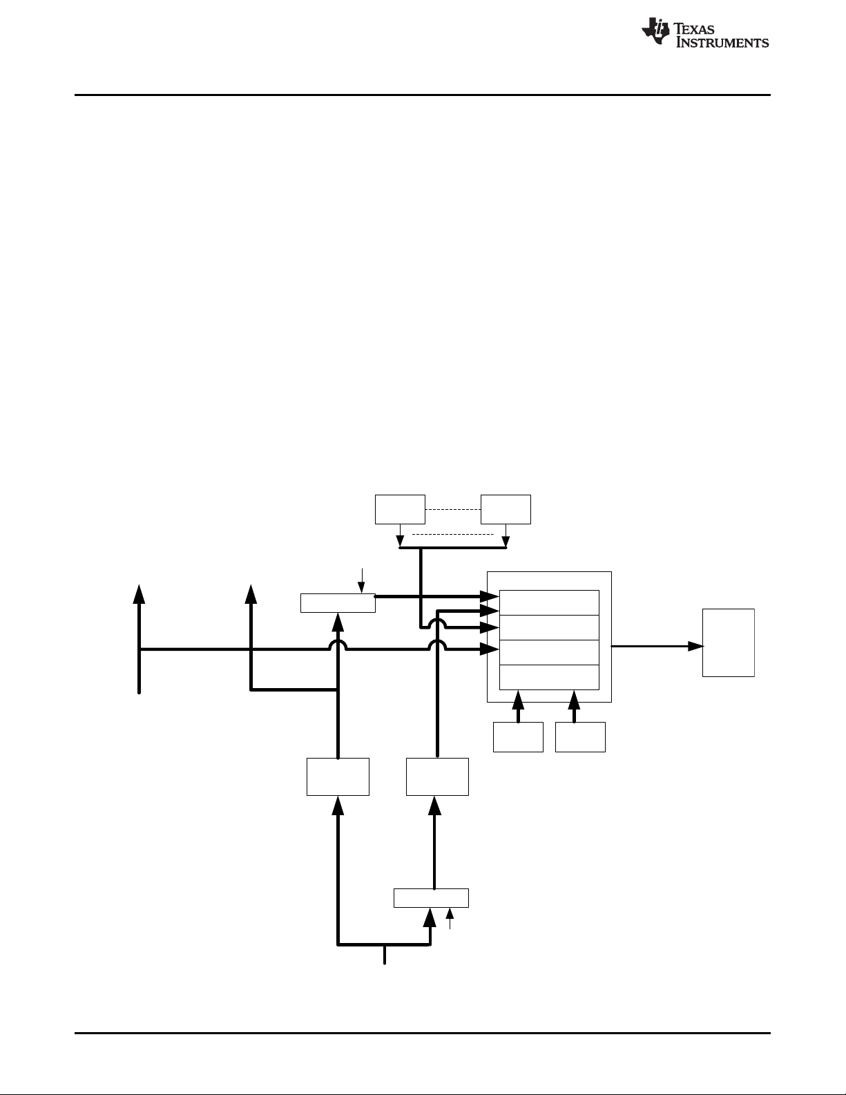
CPU Bus Compare
PD Inactivity
Monitor
VIM Bus Compare
Checker CPU
Inactivity Monitor
CPU1
(Main CPU)
CPU2
(Checker
CPU)
2 cycle delay
VIM1 VIM2
2 cycle delay
Inputs to CPU1
cpu2clk
cpu1clk
Outputs from CPU1 to
the system
Outputs from CPU2 to
the system
Safe values (values
that will force the
ZlŒWh[•}µš‰µš•
to inactive states)
CCM-R5F
Compare errors
ESM
PDx PDy
Brief Description of Elements
The following tests can be applied as a test-for-diagnostic on this module, and could be used to meet
Latent Fault Metric Requirements of ISO26262 (in combination with other diagnostics on the primary
function):
• Lockstep Compare Self-Test
• LBIST Auto-Coverage
• Software Test of PBIST
• PBIST Auto-Coverage
• Software Readback of Written Configuration (PBIST)
• Flash Data ECC
• Data ECC
6.7.1 Measures to Mitigate Common Mode Failure in CPU Subsystem
The Hercules lockstep CPU subsystem design includes multiple best practices to mitigate common mode
failure:
• Physical diversity:
– Physical core hard macros are spaced at least 100 µm apart.
– Each CPU is uniquely diversified in terms of the cell placements .
• Temporal diversity:
– Timing delay blocks are inserted to delay the operation of the CPUs by two cycles as shown in
Figure 7.
www.ti.com
Figure 7. Lockstep Temporal Diversity
30
Safety Manual for TMS570LC4x Hercules ARM Safety MCUs
Copyright © 2014–2016, Texas Instruments Incorporated
SPNU540A–May 2014–Revised September 2016
Submit Documentation Feedback
Page 31

www.ti.com
– The CPU clock domain is split into two clock trees such that clocks are delivered to the two CPUs
by separate paths.
• Power diversity:
– Each core has a dedicated 40 µm power ring.
6.7.2 Notes
• Many safety critical microcontrollers utilize a software-based test of CPU functionality as opposed to a
hardware scheme such as the TI LBIST STC. TI does not recommend such tests for a CPU of medium
to high complexity, such as the Cortex-R5F. Software-based options have higher memory cost, lower
detection capability, and longer execution times than the equivalent LBIST STC solution.
• Due to the lockstep diagnostic, it is not necessary to execute a periodic test of CPU control register
configuration. A control register disturb in one CPU should not impact the second CPU.
• Cache controller logic is included in the lockstep CPU and as such is checked on a cycle by cycle
basis.
6.8 Primary Embedded Flash
The primary embedded flash memory is a non-volatile memory residing on the CPU Interconnect
Subsystem. The primary flash memory is mainly used for CPU instruction access, though data access is
also possible. Access to the Flash memory can take multiple CPU cycles. A flash wrapper logic provides
multiple pipelined read buffers to improve CPU access time on sequential address fetches.
The following tests can be applied as diagnostics for this module (to provide diagnostic coverage on a
specific function):
• Flash Data ECC
• Hard Error Cache and Livelock
• Flash Wrapper Address ECC
• Address and Control Parity
• Boot Time Check of Flash Memory Contents by Hardware CRC
• Periodic Check of Flash Memory Contents by Hardware CRC
• Bit Multiplexing in Flash Memory Array
• Flash Sector Protection
• Periodic Software Readback of Static Configuration Registers
• Software Readback of Written Configuration
The following tests can be applied as a test-for-diagnostic on this module, and could be used to meet
Latent Fault Metric Requirements of ISO26262 (in combination with other diagnostics on the primary
function):
• Flash Wrapper Diag Mode 5 Test
• Flash Wrapper Diag Mode 7 Test
• Software Test of Parity Logic
• Software Test of Flash Sector Protection Logic
• Software Test of Hardware CRC
• CRC Auto-Coverage
• Internal Watchdog
• External Watchdog
• CPU Lockstep Compare
• SRAM Data ECC
• CPU Interconnect Hardware Checker
• Timeout Monitoring on Bus Transactions
Brief Description of Elements
SPNU540A–May 2014–Revised September 2016
Submit Documentation Feedback
Copyright © 2014–2016, Texas Instruments Incorporated
Safety Manual for TMS570LC4x Hercules ARM Safety MCUs
31
Page 32

Brief Description of Elements
6.8.1 Notes
• When exporting ECC error events from the Flash wrapper to ESM, care should be taken that the error
is not due to discarded prefetch or other branch discontinuity.
• By executing a CRC read back of Flash contents while ECC is enabled on the Flash, it is possible to
perform two diagnostics of the Flash in parallel.
• The Flash module may have unique power supply pins depending on the product configuration.
Implementation of external voltage supervision on these pins can be considered to improve system
safety integrity measures as described in the power supply section.
• The Flash module may have unique test signal pins depending on the product configuration. For
proper board level management of these signals, see the device-specific data sheet.
• To take advantage of error profiling features and to propagate error events from bus masters, the EPC
module must be initialized.
6.9 Flash EEPROM Emulation (FEE)
The Hercules platform architecture includes the capability for a separate bank of Flash memory to be used
as Flash EEPROM Emulation (FEE). FEE is used for data storage only, and cannot be used as a CPU
instruction memory. FEE is a level two memory that is accessed by the CPU over the AXI master port.
The emulation of EEPROM in the FEE memory is managed by specific FEE drivers running on the CPU.
The following tests can be applied as diagnostics for this module (to provide diagnostic coverage on a
specific function):
• FEE Data ECC
• Boot Time Check of FEE Memory Contents by Hardware CRC
• Periodic Check of FEE Memory Contents by Hardware CRC
• Bit Multiplexing in FEE Array
• FEE Sector Protection
• Periodic Software Readback of Static Configuration Registers
• Software Readback of Written Configuration
• Flash Wrapper Address ECC
The following tests can be applied as a test-for-diagnostic on this module, and could be used to meet
Latent Fault Metric Requirements of ISO26262 (in combination with other diagnostics on the primary
function):
• Flash Wrapper Diag Mode 5 Test
• Flash Wrapper Diag Mode 7 Test
• Software Test of Flash Sector Protection Logic
• Software Test of Hardware CRC
• CRC Auto-Coverage
• Internal Watchdog
• External Watchdog
• CPU Lockstep Compare
• Flash Data ECC
• SRAM Data ECC
• CPU Interconnect Hardware Checker
• Timeout Monitoring on Bus Transactions
www.ti.com
32
Safety Manual for TMS570LC4x Hercules ARM Safety MCUs
Copyright © 2014–2016, Texas Instruments Incorporated
SPNU540A–May 2014–Revised September 2016
Submit Documentation Feedback
Page 33

www.ti.com
6.9.1 Notes
• As all application FEE accesses are run through a software driver to manage EEPROM emulation, any
diagnostics must respect the functionality of the FEE driver.
• The FEE module may have unique power supply pins depending on the product configuration.
Implementation of external voltage supervision on these pins can be considered to improve system
safety integrity measures as described in the power supply section.
• The FEE module may have unique test signal pins depending on the product configuration. For proper
board level management of these signals, see the device-specific data sheet.
• To take advantage of error profiling features and to propagate error events from bus masters, the EPC
module must be initialized.
6.10 Primary Embedded SRAM
The primary embedded SRAM is a volatile memory that is accessed via the level two CPU Interconnect
Subsystem. The SRAMs are primarily used for CPU data access, though instruction access is also
possible as is access via other bus masters.
The following tests can be applied as diagnostics for this module (to provide diagnostic coverage on a
specific function):
• Data ECC
• Hard Error Cache and Livelock
• Correctable ECC Profiling
• Address and Control Bus Parity
• Redundant Address Decode
• Data and ECC Storage in Multiple Physical Banks
• Boot Time PBIST Check of Primary SRAM
• Periodic PBIST Check of Primary SRAM
• Bit Multiplexing in Primary SRAM Array
• Periodic Hardware CRC Check of Primary SRAM Contents
• Periodic Software Readback of Static Configuration Registers
• Software Readback of Written Configuration
• Scrubbing of SRAM to Correct Detected Single Bit Errors
The following tests can be applied as a test-for-diagnostic on this module, and could be used to meet
Latent Fault Metric Requirements of ISO26262 (in combination with other diagnostics on the primary
function):
• Software Test of SRAM Wrapper Redundant Address Decode and ECC
• Software Test of Parity Logic
• Software Test of PBIST
• PBIST Auto-Coverage
• Software Test of ECC Profiler
• Redundant Address Decode Self Test
• Software Test of Hardware CRC
• CRC Auto-Coverage
• Internal Watchdog
• External Watchdog
• CPU Lockstep Compare
• Flash Data ECC
Brief Description of Elements
SPNU540A–May 2014–Revised September 2016
Submit Documentation Feedback
Copyright © 2014–2016, Texas Instruments Incorporated
Safety Manual for TMS570LC4x Hercules ARM Safety MCUs
33
Page 34

Brief Description of Elements
6.10.1 Notes
• By executing a CRC read back of SRAM contents while ECC is enabled on the SRAM, it is possible to
perform two diagnostics of the SRAM in parallel.
• The SRAM module may have unique power supply pins depending on the product configuration.
Implementation of external voltage supervision on these pins can be considered to improve system
safety integrity measures as described in the power supply section.
• The redundant address decode does not provide hardware fault tolerance. As such, the logic may not
be considered fully redundant per the definition of redundancy in some safety standards.
• To take advantage of error profiling features and to propagate error events from bus masters, the EPC
module must be initialized.
6.11 CPU Interconnect Subsystem
The CPU Interconnect Subsystem is composed of a number of bridges, gaskets, communications
crossbars, and routing logic, which connects the bus masters (DMA, CPU, TUs, and so forth) to L2
memory slaves.
The following tests can be applied as diagnostics for this module (to provide diagnostic coverage on a
specific function):
• Error Trapping (Including Peripheral Slave Error Trapping)
• Information Redundancy
• Periodic Software Readback of Static Configuration Registers
• Boot Time Software Test of Basic Functionality Including Error Tests
• Periodic Software Test of Basic Functionality Including Error Tests
• Software Readback of Written Configuration
• Transmission Redundancy
• Execution of Interconnect Self-Test
• CPU Interconnect Hardware Checker
• Timeout Monitoring on Bus Transactions
• Transaction ECC (Date Lines)
• Transaction Parity (Address and Control Lines)
• Internal Watchdog
• External Watchdog
The following tests can be applied as a test-for-diagnostic on this module, and could be used to meet
Latent Fault Metric Requirements of ISO26262 (in combination with other diagnostics on the primary
function):
• CPU Lockstep Compare
• Flash Data ECC
• SRAM Data ECC
www.ti.com
6.11.1 Notes
• An end to end communications safety mechanism implemented on a networked peripheral provides an
indirect form of information redundancy diagnostic on the L2 and L3 interconnects.
• The only module in the L2 and L3 interconnect subsystem that has memory-mapped registers is the
PCR.
34
Safety Manual for TMS570LC4x Hercules ARM Safety MCUs
SPNU540A–May 2014–Revised September 2016
Copyright © 2014–2016, Texas Instruments Incorporated
Submit Documentation Feedback
Page 35

www.ti.com
6.12 Peripheral Interconnect Subsystem
The Peripheral Interconnect Subsystem is composed of a number of bridges, gaskets, communications
crossbars, and routing logic, which connects the bus masters (DMA, CPU, TUs, and so forth) to device
peripherals. This logic, while having no explicit safety critical purpose, is an intermediary in the transfer of
safety critical communications. The peripherals are further distributed among the three peripheral
segments that are mentioned below.
The following tests can be applied as diagnostics for this module (to provide diagnostic coverage on a
specific function):
• Error Trapping (Including Peripheral Slave Error Trapping)
• Peripheral Interconnect New Memory Protection Unit (NMPU)
• Information Redundancy
• Periodic Software Readback of Static Configuration Registers
• Boot Time Software Test of Basic Functionality Including Error Tests
• Periodic Software Test of Basic Functionality Including Error Tests
• Software Readback of Written Configuration
• Transmission Redundancy
• Internal Watchdog
• External Watchdog
The following tests can be applied as a test-for-diagnostic on this module, and could be used to meet
Latent Fault Metric Requirements of ISO26262 (in combination with other diagnostics on the primary
function):
• CPU Lockstep Compare
• Flash Data ECC
• SRAM Data ECC
Brief Description of Elements
6.13 Peripheral Central Resource 1 (PCR1)
The Peripheral Central Resource 1 refers to the interconnect that connects the bus masters (CPU , DMA
and so forth) to selected system peripherals, debug, test, emulation and instrumentation logic on the first
segment located beneath the Peripheral Interconnect Subsystem.
The following tests can be applied as diagnostics for this module (to provide diagnostic coverage on a
specific function):
• Error Trapping (Including Peripheral Slave Error Trapping)
• PCR Access Management: Protection Mode and MasterID Filtering
• Information Redundancy
• Periodic Software Readback of Static Configuration Registers
• Boot Time Software Test of Basic Functionality Including Error Tests
• Periodic Software Test of Basic Functionality Including Error Tests
• Software Readback of Written Configuration
• Transmission Redundancy
• Internal Watchdog
• External Watchdog
The following tests can be applied as a test-for-diagnostic on this module, and could be used to meet
Latent Fault Metric Requirements of ISO26262 (in combination with other diagnostics on the primary
function):
• CPU Lockstep Compare
• Flash Data ECC
• SRAM Data ECC
SPNU540A–May 2014–Revised September 2016
Submit Documentation Feedback
Copyright © 2014–2016, Texas Instruments Incorporated
Safety Manual for TMS570LC4x Hercules ARM Safety MCUs
35
Page 36

Brief Description of Elements
6.14 Peripheral Central Resource 2 (PCR2)
The Peripheral Central Resource 2 refers to the interconnect that connects the bus masters (CPU , DMA
and so forth) to selected high speed and motor control peripherals on the second segment located
beneath the Peripheral Interconnect Subsystem.
The following tests can be applied as diagnostics for this module (to provide diagnostic coverage on a
specific function):
• Error Trapping (Including Peripheral Slave Error Trapping)
• PCR Access Management: Protection Mode and MasterID Filtering
• Information Redundancy
• Periodic Software Readback of Static Configuration Registers
• Boot Time Software Test of Basic Functionality Including Error Tests
• Periodic Software Test of Basic Functionality Including Error Tests
• Software Readback of Written Configuration
• Transmission Redundancy
• Internal Watchdog
• External Watchdog
The following tests can be applied as a test-for-diagnostic on this module, and could be used to meet
Latent Fault Metric Requirements of ISO26262 (in combination with other diagnostics on the primary
function):
• CPU Lockstep Compare
• Flash Data ECC
• SRAM Data ECC
www.ti.com
6.15 Peripheral Central Resource 3 (PCR3)
The Peripheral Central Resource 3 refers to the interconnect that connects the bus masters (DMA, CPU,
and so forth) to user peripherals on the third segment located beneath the Peripheral Interconnect
Subsystem.
The following tests can be applied as diagnostics for this module (to provide diagnostic coverage on a
specific function):
• Error Trapping (Including Peripheral Slave Error Trapping)
• PCR Access Management: Protection Mode and MasterID Filtering
• Information Redundancy
• Periodic Software Readback of Static Configuration Registers
• Boot Time Software Test of Basic Functionality Including Error Tests
• Periodic Software Test of Basic Functionality Including Error Tests
• Software Readback of Written Configuration
• Transmission Redundancy
• Internal Watchdog
• External Watchdog
The following tests can be applied as a test-for-diagnostic on this module, and could be used to meet
Latent Fault Metric Requirements of ISO26262 (in combination with other diagnostics on the primary
function):
• CPU Lockstep Compare
• Flash Data ECC
• SRAM Data ECC
36
Safety Manual for TMS570LC4x Hercules ARM Safety MCUs
Copyright © 2014–2016, Texas Instruments Incorporated
SPNU540A–May 2014–Revised September 2016
Submit Documentation Feedback
Page 37

www.ti.com
6.16 EFuse Static Configuration
The Hercules platform devices support a manufacturing time configuration of certain functionality (such as
trim values for analog macros) via one time programmable (OTP) EFuse structures. The EFuses are read
automatically after power-on reset by an autoload function.
The following tests can be applied as diagnostics for this module (to provide diagnostic coverage on a
specific function):
• Autoload Self Test
• E-Fuse ECC
• Periodic Software Readback of Static Configuration Registers
• Software Readback of Written Configuration
The following tests can be applied as a test-for-diagnostic on this module, and could be used to meet
Latent Fault Metric Requirements of ISO26262 (in combination with other diagnostics on the primary
function):
• Autoload Self Test Auto-Coverage
• EFuse ECC Logic Self Test
• Internal Watchdog
• External Watchdog
• CPU Lockstep Compare
• Flash Data ECC
• SRAM Data ECC
Brief Description of Elements
6.17 OTP Static Configuration
The Hercules platform devices support a manufacturing time configuration of certain functionality (such as
endianness and the initial configuration of power domains after reset) via one time programmable Flash
memory. The OTP configuration values are read automatically after warm reset by an autoload function.
The following tests can be applied as diagnostics for this module (to provide diagnostic coverage on a
specific function):
• Autoload Self Test
• OTP ECC
• Periodic Software Readback of Static Configuration Registers
• Software Readback of Written Configuration
• Boot Time Hardware CRC Check of OTP Contents
• Periodic Hardware CRC Check of OTP Contents
• Bit Multiplexing in Flash Memory Array
• Flash Sector Protection
The following tests can be applied as a test-for-diagnostic on this module, and could be used to meet
Latent Fault Metric Requirements of ISO26262 (in combination with other diagnostics on the primary
function):
• Software Test of Flash Sector Protection Logic
• Software Test of Hardware CRC
• CRC Auto-Coverage
• Flash Wrapper Diag Mode 5 Test
• Flash Wrapper Diag Mode 7 Test
• Internal Watchdog
• External Watchdog
• CPU Lockstep Compare
• Flash Data ECC
SPNU540A–May 2014–Revised September 2016
Submit Documentation Feedback
Copyright © 2014–2016, Texas Instruments Incorporated
Safety Manual for TMS570LC4x Hercules ARM Safety MCUs
37
Page 38

Brief Description of Elements
• SRAM Data ECC
6.17.1 Notes
The OTP Flash memory used for storage of the configuration words can be read by the CPU.
6.18 I/O Multiplexing Module (IOMM)
The I/O multiplexing module (IOMM) provides software configurable mapping of internal module I/O
functionality to device pins.
The following tests can be applied as diagnostics for this module (to provide diagnostic coverage on a
specific function):
• Locking Mechanism For Control Registers
• Master ID Filtering
• Error Trapping
• Periodic Software Readback of Static Configuration Registers
• Boot Time Software Test of Function Using I/O Loopback Including Error Tests
• Periodic Software Test of Function Using I/O Loopback Including Error Tests
• Software Readback of Written Configuration
The following tests can be applied as a test-for-diagnostic on this module, and could be used to meet
Latent Fault Metric Requirements of ISO26262 (in combination with other diagnostics on the primary
function):
• Internal Watchdog
• External Watchdog
• CPU Lockstep Compare
• Flash Data ECC
• SRAM Data ECC
www.ti.com
6.18.1 Notes
Software testing of the IOMM can be combined with peripheral loopback testing.
6.19 Vectored Interrupt Module (VIM)
The vectored interrupt module (VIM) is used to interface peripheral interrupts to the Cortex-R5F CPU. The
VIM provides programmable interrupt prioritization, masking, and sleep mode wake up functionality. The
VIM includes a local SRAM that is used to hold the address of the interrupt handler per channel. Two
VIMs (VIM1 and VIM2) are implemented on this device. For safety diagnostics purposes the VIMs (VIM1
and VIM2) are implemented and run in lock step pairs .
The following tests can be applied as diagnostics for this module (to provide diagnostic coverage on a
specific function):
• VIM SRAM Data ECC
• Boot Time PBIST Check of VIM SRAM
• Periodic PBIST Check of VIM SRAM
• Bit Multiplexing in VIM SRAM Array
• Periodic Hardware CRC Check of VIM SRAM Contents
• Boot Time Software Test of VIM Functionality Including Error Tests
• Periodic Software Test of VIM Functionality Including Error Tests
• Periodic Software Readback of Static Configuration Registers
• Software Readback of Written Configuration
• VIM Lockstep Compare
38
Safety Manual for TMS570LC4x Hercules ARM Safety MCUs
Copyright © 2014–2016, Texas Instruments Incorporated
SPNU540A–May 2014–Revised September 2016
Submit Documentation Feedback
Page 39

www.ti.com
• Internal Watchdog
• External Watchdog
• CPU Memory Protection Unit (MPU)
• Online Profiling Using PMU
The following tests can be applied as a test-for-diagnostic on this module, and could be used to meet
Latent Fault Metric Requirements of ISO26262 (in combination with other diagnostics on the primary
function):
• Software test of ECC Logic
• PBIST Test of ECC Bit Memory
• Software Test of Hardware CRC
• CRC Auto-Coverage
• Software Test of PBIST
• PBIST Auto-Coverage
• CPU Lockstep Compare
• Flash Data ECC
• SRAM Data ECC
• Lockstep Compare Self-Test
6.19.1 Notes
Care should be taken to optimize any VIM software diagnostics for the mode of operation - legacy IRQ
and FIQ, legacy vectored, or fully hardware vectored.
Brief Description of Elements
6.20 Real Time Interrupt (RTI)
The real time interrupt (RTI) module provides the operating system timer for the device. The OS timer
function is used to generate internal event triggers or interrupts as needed to provide periodic operation of
safety critical functions.
The following tests can be applied as diagnostics for this module (to provide diagnostic coverage on a
specific function):
• 1oo2 Software Voting Using Secondary Free Running Counter
• Periodic Software Readback of Static Configuration Registers
• Software Readback of Written Configuration
The following tests can be applied as a test-for-diagnostic on this module, and could be used to meet
Latent Fault Metric Requirements of ISO26262 (in combination with other diagnostics on the primary
function):
• External Watchdog
• CPU Lockstep Compare
• Flash Data ECC
• SRAM Data ECC
6.20.1 Notes
When using one counter to the operating system time base counter, a diverse configuration of clock
source, scaling factor, and so forth can be used to reduce probability of common mode failure.
The FlexRay Network Time Unit (NTU) can be used to serve as the clock source for the operating system
timer. This can be utilized for network synchronization of safety critical tasks. If the NTU detects loss of
synch with the network, system can automatically revert to local clock sources.
SPNU540A–May 2014–Revised September 2016
Submit Documentation Feedback
Copyright © 2014–2016, Texas Instruments Incorporated
Safety Manual for TMS570LC4x Hercules ARM Safety MCUs
39
Page 40

Brief Description of Elements
6.21 Direct Memory Access (DMA)
The direct memory access (DMA) module is used to move data from one location to another inside the
system. This is typically used for peripheral configuration (Flash and SRAM to peripheral transfer) and
peripheral data update (peripheral buffer memory transfer to CPU SRAM for processing). The DMA is
typically used by the operating system to offload bus transactions from the CPU in order to improve overall
system performance. The DMA has a local SRAM that is used for channel control information.
The following tests can be applied as diagnostics for this module (to provide diagnostic coverage on a
specific function):
• Memory Protection Unit for Bus Master Accesses
• Non-Privileged Bus Master Access
• Information Redundancy Techniques
• DMA SRAM Data ECC
• Boot Time PBIST Check of DMA SRAM
• Periodic PBIST Check of DMA SRAM
• Bit Multiplexing in DMA SRAM Array
• Periodic Hardware CRC Check of DMA SRAM Contents
• Periodic Software Readback of Static Configuration Registers
• Boot Time Software Test of Basic Functinality Including Error Tests
• Periodic Software Test of Basic Functinality Including Error Tests
• Software Readback of Written Configuration
• Transmission Redundancy
• Peripheral Interconnect New Memory Protection Unit (NMPU)
• Hardware Disable of JTAG Port
The following tests can be applied as a test-for-diagnostic on this module, and could be used to meet
Latent Fault Metric Requirements of ISO26262 (in combination with other diagnostics on the primary
function):
• Software test of ECC Logic
• PBIST Test of ECC Bit Memory
• Software Test of Hardware CRC
• CRC Auto-Coverage
• Software Test of PBIST
• PBIST Auto-Coverage
• Software Test of MPU Functionality
• Multi-Bit Keyed Self-Correctable High-Integrity Bits
• Internal Watchdog
• External Watchdog
• CPU Lockstep Compare
• Flash Data ECC
• SRAM Data ECC
www.ti.com
6.22 High-End Timer (N2HET), HET Transfer Unit (HTU)
The N2HET module is a programmable timer with input/output capabilities. The N2HET is implemented as
a simple RISC processor with instruction set dedicated for timing operations. Complex inputs can be
captured and pre-processed by the N2HET for later processing by the CPU. Output generation is typically
pulse width modulation (PWM), but may also be simple general-purpose input/output (GIO) type signals.
Each N2HET has a dedicated micro DMA controller called HTU. The HTU provides a high bandwidth
connection for data transfer to and from N2HET from and to CPU memories.
40
Safety Manual for TMS570LC4x Hercules ARM Safety MCUs
Copyright © 2014–2016, Texas Instruments Incorporated
SPNU540A–May 2014–Revised September 2016
Submit Documentation Feedback
Page 41

www.ti.com
The following tests can be applied as diagnostics for this module (to provide diagnostic coverage on a
specific function):
• Memory Protection Unit for HTU Bus Master Accesses
• Information Redundancy Techniques
• Use of DCC as Program Sequence Watchdog
• Monitoring by Second N2HET
• Boot Time Software Test of Function Using I/O Loopback
• Periodic Software Test of Function Using I/O Loopback
• N2HET/HTU SRAM Data Parity
• Boot Time PBIST Check of N2HET/HTU SRAM
• Periodic PBIST Check of N2HET/HTU SRAM
• Bit Multiplexing in N2HET/HTU SRAM Array
• Periodic Hardware CRC Check of N2HET/HTU SRAM Contents
• Periodic Software Readback of Static Configuration Registers
• Software Readback of Written Configuration
• Transmission Redundancy for Transfer Unit
• Boot Time Software test of Function Using I/O Checking In GIO Mode
• Periodic Software test of Function Using I/O Checking In GIO Mode
• Information Redundancy Techniques (while in GIO Mode)
• Hardware Disable of JTAG Port
The following tests can be applied as a test-for-diagnostic on this module, and could be used to meet
Latent Fault Metric Requirements of ISO26262 (in combination with other diagnostics on the primary
function):
• Software test of Parity Logic
• PBIST Test of Parity Bit Memory
• Software Test of Hardware CRC
• CRC Auto-Coverage
• Software Test of PBIST
• PBIST Auto-Coverage
• Software Test of MPU Functionality
• Software Test of DCC Functionality
• Boot Time Execution of LBIST STC
• Periodic Execution of LBIST STC
• Internal Watchdog
• External Watchdog
• CPU Lockstep Compare
• Flash Data ECC
• SRAM Data ECC
• LBIST Auto-Coverage
Brief Description of Elements
6.22.1 Notes
• Information redundancy techniques used on N2HET can be extended to also cover the HTU bus
master operation.
• To reduce probability of common mode failure, user should consider implementing multiple channels
(information redundancy) using non adjacent pins.
SPNU540A–May 2014–Revised September 2016
Submit Documentation Feedback
Copyright © 2014–2016, Texas Instruments Incorporated
Safety Manual for TMS570LC4x Hercules ARM Safety MCUs
41
Page 42

Brief Description of Elements
6.23 Multi-Buffered Analog-to-Digital Converter (MibADC)
The MibADC module is used to convert analog inputs into digital values. Results are stored in internal
SRAM buffers for later transfer by DMA or CPU. The Hercules device family products implement two
modules with shared channels used for fast conversion (ping-pong method). Systems implementing two
channels using the dual ADC converters may be able to claim fault tolerance in application.
The following tests can be applied as diagnostics for this module (to provide diagnostic coverage on a
specific function):
• Hardware Disable of JTAG Port
• Boot Time Input Self Test
• Boot Time MibADC Calibration
• Periodic MibADC Calibration
• MibADC Information Redundancy Techniques
• MibADC SRAM Data Parity
• Boot Time PBIST Check of MibADC SRAM
• Periodic PBIST Check of MibADC SRAM
• Bit Multiplexing in MibADC SRAM Array
• Periodic Hardware CRC Check of MibADC SRAM Contents
• Periodic Software Readback of Static Configuration Registers
• Software Readback of Written Configuration
• Boot Time Software Test of Function Using I/O Checking In GIO Mode
• Periodic Software Test of Function Using I/O Checking In GIO Mode
• Information Redundancy Techniques (while in GIO Mode)
The following tests can be applied as a test-for-diagnostic on this module, and could be used to meet
Latent Fault Metric Requirements of ISO26262 (in combination with other diagnostics on the primary
function):
• Software test of Parity Logic
• PBIST Test of Parity Bit Memory
• Software Test of Hardware CRC
• CRC Auto-Coverage
• Software Test of PBIST
• PBIST Auto-Coverage
• Internal Watchdog
• External Watchdog
• CPU Lockstep Compare
• Flash Data ECC
• SRAM Data ECC
www.ti.com
6.23.1 Notes
• The MibADC module may be referred to as MibADC (Multi Buffered ADC) in some documents.
• ADC module voltages should be supervised as noted in Power Supply
• To reduce probability of common mode failure, user should consider implementing multiple channels
(information redundancy) using non adjacent pins.
6.24 Enhanced Pulse Width Modulators (ePWM)
The enhanced pulse width modulator (ePWM) peripheral is a key element in controlling many of the power
electronic systems found in both commercial and industrial equipments. The features supported by the
ePWM make it especially suitable for digital motor control.
42
Safety Manual for TMS570LC4x Hercules ARM Safety MCUs
Copyright © 2014–2016, Texas Instruments Incorporated
SPNU540A–May 2014–Revised September 2016
Submit Documentation Feedback
Page 43

www.ti.com
The following tests can be applied as diagnostics for this module (to provide diagnostic coverage on a
specific function):
• Boot Time Software Test of Function Including Error Tests
• Periodic Software Test of Function Including Error Tests
• Information Redundancy Techniques
• Monitoring by eCAP or N2HET
• Periodic Software Readback of Static Configuration Registers
• Software Readback of Written Configuration
The following tests can be applied as a test-for-diagnostic on this module, and could be used to meet
Latent Fault Metric Requirements of ISO26262 (in combination with other diagnostics on the primary
function):
• Internal Watchdog
• External Watchdog
• CPU Lockstep Compare
• Flash Data ECC
• SRAM Data ECC
• Boot Time Software Test of eCAP Function
• Periodic Software Test of eCAP Function
• Boot Time Test of N2HET Function Including I/O Loopback
• Periodic Test of N2HET Function Including I/O Loopback
Brief Description of Elements
6.25 Enhanced Capture (eCAP)
The enhanced Capture (eCAP) module provides input capture functionality for systems where accurate
timing of external events is important.
The following tests can be applied as diagnostics for this module (to provide diagnostic coverage on a
specific function):
• Boot Time Software Test of Function Including Error Tests
• Periodic Software Test of Function Including Error Tests
• Information Redundancy Techniques
• Periodic Software Readback of Static Configuration Registers
• Software Readback of Written Configuration
Information Redundancy Techniques (while in PWM Mode)
• Monitoring by eCAP or N2HET (while in PWM Mode)
The following tests can be applied as a test-for-diagnostic on this module, and could be used to meet
Latent Fault Metric Requirements of ISO26262 (in combination with other diagnostics on the primary
function):
• Internal Watchdog
• External Watchdog
• CPU Lockstep Compare
• Flash Data ECC
• SRAM Data ECC
6.25.1 Notes
• If using the eCAP in PWM output mode, see the guidance for the Section 6.24.
• N2HET channels can be used for input capture as a hardware diverse second channel to implement
information redundancy with reduced probability of common mode failure.
SPNU540A–May 2014–Revised September 2016
Submit Documentation Feedback
Copyright © 2014–2016, Texas Instruments Incorporated
Safety Manual for TMS570LC4x Hercules ARM Safety MCUs
43
Page 44

Brief Description of Elements
6.26 Enhanced Quadrature Encoder Pulse (eQEP)
The enhanced quadrature encoder pulse (eQEP) module is used for direct interface with a linear or rotary
incremental encoder to get position, direction, and speed information from a rotating machine for use in a
high-performance motion and position-control system.
The following tests can be applied as diagnostics for this module (to provide diagnostic coverage on a
specific function):
• Boot Time Software Test of Function Including Error Tests
• Periodic Software Test of Function Including Error Tests
• Information Redundancy Techniques
• Periodic Software Readback of Static Configuration Registers
• Software Readback of Written Configuration
• Quadrature Watchdog
The following tests can be applied as a test-for-diagnostic on this module, and could be used to meet
Latent Fault Metric Requirements of ISO26262 (in combination with other diagnostics on the primary
function):
• Software Test of Quadrature Watchdog Functionality
• Internal Watchdog
• External Watchdog
• CPU Lockstep Compare
• Flash Data ECC
• SRAM Data ECC
www.ti.com
6.26.1 Notes
Use of a sensorless positioning algorithm can provide information redundancy through plausibility
checking of eQEP results.
6.27 Multi Buffered Serial Peripheral Interface (MibSPI)
The MibSPI modules provide serial I/O compliant to the MibSPI protocol. MibSPI communications are
typically used for communication to smart sensors and actuators, serial memories, and external logic such
as a watchdog device. The MibSPI modules contain internal SRAM buffers. If not used for MibSPI
communication, the MibSPI modules support the usage of their I/O as general purpose I/O.
The following tests can be applied as diagnostics for this module (to provide diagnostic coverage on a
specific function):
• Boot Time Software Test of Function Using I/O Loopback
• Periodic Software Test of Function Using I/O Loopback
• Parity in Message
• Information Redundancy Techniques
• MibSPI SRAM ECC
• Boot Time PBIST Check of MibSPI SRAM
• Periodic PBIST Check of MibSPI SRAM
• Bit Multiplexing in MibSPI SRAM Array
• Periodic Hardware CRC Check of MibSPI SRAM Contents
• Periodic Software Readback of Static Configuration Registers
• Software Readback of Written Configuration
• Transmission Redundancy
• Data Overrun Error Detection
• Bit Error Detection
44
Safety Manual for TMS570LC4x Hercules ARM Safety MCUs
Copyright © 2014–2016, Texas Instruments Incorporated
SPNU540A–May 2014–Revised September 2016
Submit Documentation Feedback
Page 45

www.ti.com
• Slave Desync Detection
• Slave Timeout Detection
• Data Length Error Detection
• Hardware Disable of JTAG Port
• Boot Time Software Test of Function Using I/O Checking In GIO Mode
• Periodic Software Test of Function Using I/O Checking In GIO Mode
• Information Redundancy Techniques (while in GIO Mode)
The following tests can be applied as a test-for-diagnostic on this module, and could be used to meet
Latent Fault Metric Requirements of ISO26262 (in combination with other diagnostics on the primary
function):
• Software test of ECC Logic
• PBIST Test of ECC Bit Memory
• Software Test of Hardware CRC
• CRC Auto-Coverage
• Software Test of PBIST
• PBIST Auto-Coverage
• Internal Watchdog
• External Watchdog
• CPU Lockstep Compare
• Flash Data ECC
• SRAM Data ECC
Brief Description of Elements
6.27.1 Notes
It is possible to use the MIBSPI in standard SPI mode.
6.28 Inter-Integrated Circuit (I2C)
The I2C module provides a multi-master serial bus compliant to the I2C protocol.
The following tests can be applied as diagnostics for this module (to provide diagnostic coverage on a
specific function):
• Boot Time Software Test of Function Using I/O Loopback
• Periodic Software Test of Function Using I/O Loopback
• Information Redundancy Techniques
• Periodic Software Readback of Static Configuration Registers
• Software Readback of Written Configuration
• Transmission Redundancy
• Hardware Disable of JTAG Port
• Boot Time Software Test of Function Using I/O Checking In GIO Mode
• Periodic Software Test of Function Using I/O Checking In GIO Mode
• Information Redundancy Techniques (while in GIO Mode)
The following tests can be applied as a test-for-diagnostic on this module, and could be used to meet
Latent Fault Metric Requirements of ISO26262 (in combination with other diagnostics on the primary
function):
• Internal Watchdog
• External Watchdog
• CPU Lockstep Compare
• Flash Data ECC
SPNU540A–May 2014–Revised September 2016
Submit Documentation Feedback
Copyright © 2014–2016, Texas Instruments Incorporated
Safety Manual for TMS570LC4x Hercules ARM Safety MCUs
45
Page 46

Brief Description of Elements
• SRAM Data ECC
6.29 Serial Communication Interface (SCI)
The SCI module provides serial I/O capability for typical asynchronous serial communication interface
(SCI) protocols, such as UART. Depending on the serial protocol used, an external transceiver may be
necessary.
The following tests can be applied as diagnostics for this module (to provide diagnostic coverage on a
specific function):
• Boot Time Software Test of Function Using I/O Loopback
• Periodic Software Test of Function Using I/O Loopback
• Information Redundancy Techniques
• Periodic Software Readback of Static Configuration Registers
• Software Readback of Written Configuration
• Transmission Redundancy
• Overrun Error Detection
• Frame Error Detection
• Bit Error Detection
• Parity in Message
• Hardware Disable of JTAG Port
• Boot Time Software Test of Function Using I/O Checking In GIO Mode
• Periodic Software Test of Function Using I/O Checking In GIO Mode
• Information Redundancy Techniques (while in GIO Mode)
The following tests can be applied as a test-for-diagnostic on this module, and could be used to meet
Latent Fault Metric Requirements of ISO26262 (in combination with other diagnostics on the primary
function):
• Internal Watchdog
• External Watchdog
• CPU Lockstep Compare
• Flash Data ECC
• SRAM Data ECC
www.ti.com
6.30 Local Interconnect Network (LIN)
The LIN module provides serial I/O compliant to the LIN protocol. LIN is a low throughput time triggered
protocol. The module can also be configured in SCI mode and used as a general purpose serial port. An
external transceiver is used for LIN communications.
The following tests can be applied as diagnostics for this module (to provide diagnostic coverage on a
specific function):
• Boot Time Software Test of Function Using I/O Loopback
• Periodic Software Test of Function Using I/O Loopback
• Information Redundancy Techniques
• Periodic Software Readback of Static Configuration Registers
• Software Readback of Written Configuration
• Transmission Redundancy
• Overrun Error Detection
• Frame Error Detection
• Physical Bus Error Detection
• No-Response Error Detection
46
Safety Manual for TMS570LC4x Hercules ARM Safety MCUs
Copyright © 2014–2016, Texas Instruments Incorporated
SPNU540A–May 2014–Revised September 2016
Submit Documentation Feedback
Page 47

www.ti.com
• Bit Error Detection
• Checksum Error Detection
• Parity in Message
• Hardware Disable of JTAG Port
• Boot Time Software Test of Function Using I/O Checking In GIO Mode
• Periodic Software Test of Function Using I/O Checking In GIO Mode
• Information Redundancy Techniques (while in GIO Mode)
The following tests can be applied as a test-for-diagnostic on this module, and could be used to meet
Latent Fault Metric Requirements of ISO26262 (in combination with other diagnostics on the primary
function):
• Internal Watchdog
• External Watchdog
• CPU Lockstep Compare
• Flash Data ECC
• SRAM Data ECC
6.30.1 Notes
When using the LIN module in SCI mode, see Section 6.29.
6.31 Controller Area Network (DCAN)
The DCAN interface provides medium throughput networking with event based triggering, compliant to the
CAN protocol. The DCAN modules requires an external transceiver to operate on the CAN network.
The following tests can be applied as diagnostics for this module (to provide diagnostic coverage on a
specific function):
• Boot Time Software Test of Function Using I/O Loopback
• Periodic Software Test of Function Using I/O Loopback
• Information Redundancy Techniques Including End to End Safing
• DCAN SRAM Data ECC
• Boot Time PBIST Check of DCAN SRAM
• Periodic PBIST Check of DCAN SRAM
• Bit Multiplexing in DCAN SRAM Array
• Periodic Hardware CRC Check of DCAN SRAM Contents
• Periodic Software Readback of Static Configuration Registers
• Software Readback of Written Configuration
• Transmission Redundancy
• Stuff Error Detection
• Form Error Detection
• Acknowledge Error Detection
• Bit Error Detection
• CAN Protocol CRC in Message
• Hardware Disable of JTAG Port
• Boot Time Software Test of Function Using I/O Checking In GIO Mode
• Periodic Software Test of Function Using I/O Checking In GIO Mode
• Information Redundancy Techniques (while in GIO Mode)
The following tests can be applied as a test-for-diagnostic on this module, and could be used to meet
Latent Fault Metric Requirements of ISO26262 (in combination with other diagnostics on the primary
function):
Brief Description of Elements
SPNU540A–May 2014–Revised September 2016
Submit Documentation Feedback
Copyright © 2014–2016, Texas Instruments Incorporated
Safety Manual for TMS570LC4x Hercules ARM Safety MCUs
47
Page 48

Brief Description of Elements
• Software test of ECC Logic
• PBIST Test of ECC Bit Memory
• Software Test of Hardware CRC
• CRC Auto-Coverage
• Software Test of PBIST
• PBIST Auto-Coverage
• Internal Watchdog
• External Watchdog
• CPU Lockstep Compare
• Flash Data ECC
• SRAM Data ECC
6.32 FlexRay, FlexRay Transfer Unit (FTU)
The FlexRay interface provides data interconnect with pre-defined, time triggered (TDMA) slots for each
connected node to communicate. The FlexRay network supports higher data throughput than legacy CAN
networks and is compliant to the FlexRay protocol. In typical automotive usage, the FlexRay network is
the backbone network used for connection to a chassis and safety system such that information can be
passed between safety critical systems.
The device provides two FlexRay channels. Depending on configuration, the device could connect two
different FlexRay networks and act as a gateway, or the device could act as two nodes on the same
FlexRay network if multiple time slots are required in the system network concept. An external transceiver
device is needed to provide the physical layer connection to the FlexRay network. A separate PLL is
integrated to generate the frequencies required for the FlexRay network.
The Hercules FlexRay module includes dedicated DMA capability in the FlexRay Transfer Unit (FTU).
The following tests can be applied as diagnostics for this module (to provide diagnostic coverage on a
specific function):
• Memory Protection Unit for FTU Bus Master Accesses
• Non-Privileged Bus Master Accesses
• Boot Time Software Test of Function Using I/O Loopback in Transceiver/PHY
• Periodic Software Test of Function Using I/O Loopback in Transceiver/PHY
• Information Redundancy Techniques Including End to End Safing
• 1oo2 Voting Using Both FlexRay Channels
• FlexRay and FTU SRAM Data ECC
• Boot Time PBIST Check of FlexRay and FTU SRAM
• Periodic PBIST Check of FlexRay and FTU SRAM
• Bit Multiplexing in FlexRay and FTU SRAM Array
• Periodic Hardware CRC Check of FlexRay and FTU SRAM Contents
• Periodic Software Readback of Static Configuration Registers
• Software Readback of Written Configuration
• Transmission Redundancy
• CRC in Message
• FIFO Overrun Detection
• Sync Frames Below Minimum / Sync Frame Overflow
• CCF Clock Correction Failure Detection
• Message Handler Error Detection
• EDA / EDB Error Detection
• Transmission Across Boundary Error Detection
www.ti.com
48
Safety Manual for TMS570LC4x Hercules ARM Safety MCUs
Copyright © 2014–2016, Texas Instruments Incorporated
SPNU540A–May 2014–Revised September 2016
Submit Documentation Feedback
Page 49

www.ti.com
• Hardware Disable of JTAG Port
The following tests can be applied as a test-for-diagnostic on this module, and could be used to meet
Latent Fault Metric Requirements of ISO26262 (in combination with other diagnostics on the primary
function):
• Software test of ECC Logic
• PBIST Test of ECC Bit Memory
• Software Test of Hardware CRC
• CRC Auto-Coverage
• Software Test of PBIST
• PBIST Auto-Coverage
• Software Test of MPU Functionality
• Internal Watchdog
• External Watchdog
• CPU Lockstep Compare
• Flash Data ECC
• SRAM Data ECC
6.32.1 Notes
• The FlexRay communication controller does not have the capability to calculate the header CRC. The
host provides the header CRCs for all transmit buffers.
• Due to the deterministic nature of FlexRay transmissions, this interface is preferred for transmitting
timing sensitive sensor data and synchronization of safety critical tasks across multiple network nodes.
Brief Description of Elements
6.33 General-Purpose Input/Output (GIO)
The GIO module provides digital input capture and digital input/output. There is no processing function in
this block. The GIO is typically used for static or rarely changed outputs, such as transceiver enable
signals, warning lights, and so forth. The GIO can also be used to provide external interrupt input
capabilities.
The following tests can be applied as diagnostics for this module (to provide diagnostic coverage on a
specific function):
• Boot Time Software Test of Function Using I/O Checking In GIO Mode
• Periodic Software Test of Function Using I/O Checking In GIO Mode
• Information Redundancy Techniques
• Periodic Software Readback of Static Configuration Registers
• Software Readback of Written Configuration
The following tests can be applied as a test-for-diagnostic on this module, and could be used to meet
Latent Fault Metric Requirements of ISO26262 (in combination with other diagnostics on the primary
function):
• Internal Watchdog
• External Watchdog
• CPU Lockstep Compare
• Flash Data ECC
• SRAM Data ECC
6.33.1 Notes
To reduce probability of common mode failure, the user should consider implementing multiple channels
using non adjacent pins.
SPNU540A–May 2014–Revised September 2016
Submit Documentation Feedback
Copyright © 2014–2016, Texas Instruments Incorporated
Safety Manual for TMS570LC4x Hercules ARM Safety MCUs
49
Page 50

Brief Description of Elements
6.34 Ethernet
The Hercules platform includes an Ethernet media access controller (EMAC) and physical layer (PHY)
device management data input/output (MDIO) module. These modules allow connection of the Hercules
MCU to a 10 and 100 Mb Ethernet network. The Ethernet network provides higher network throughput
than LIN, CAN, or FlexRay.
The following tests can be applied as diagnostics for this module (to provide diagnostic coverage on a
specific function):
• Non-Privileged Bus Master Access
• Boot Time Software Test of Function Using I/O Loopback in PHY
• Periodic Software Test of Function Using I/O Loopback in PHY
• Information Redundancy Techniques
• Boot Time PBIST Check of Ethernet SRAM
• Periodic PBIST Check of Ethernet SRAM
• Bit Multiplexing in Ethernet SRAM Array
• Periodic Hardware CRC Check of Ethernet SRAM Contents
• Periodic Software Readback of Static Configuration Registers
• Software Readback of Written Configuration
• Transmission Redundancy
• CRC in Message
• Ethernet Alignment Error Detection
• Ethernet Physical Layer Fault
• Peripheral Interconnect New Memory Protection Unit (NMPU)
• Hardware Disable of JTAG Port
The following tests can be applied as a test-for-diagnostic on this module, and could be used to meet
Latent Fault Metric Requirements of ISO26262 (in combination with other diagnostics on the primary
function):
• Software Test of Hardware CRC
• CRC Auto-Coverage
• Software Test of PBIST
• PBIST Auto-Coverage
• Software test of New Memory Protection Unit (NMPU) Function
• Internal Watchdog
• External Watchdog
• CPU Lockstep Compare
• Flash Data ECC
• SRAM Data ECC
www.ti.com
6.35 External Memory Interface (EMIF)
The external memory interface is used to provide device access to off-chip memories or devices, which
support a memory interface. Support is provided for both synchronous (SDRAM) and asynchronous (NOR
Flash, SRAM) memories.
The following tests can be applied as diagnostics for this module (to provide diagnostic coverage on a
specific function):
• Information Redundancy Techniques
• Boot Time Hardware CRC Check of External Memory
• Periodic Hardware CRC Check of External Memory
• Periodic Software Readback of Static Configuration Registers
50
Safety Manual for TMS570LC4x Hercules ARM Safety MCUs
Copyright © 2014–2016, Texas Instruments Incorporated
SPNU540A–May 2014–Revised September 2016
Submit Documentation Feedback
Page 51

www.ti.com
• Software Readback of Written Configuration
• Transmission Redundancy
• Hardware Disable of JTAG Port
• Timeout Monitoring on Bus Transactions
• CPU Interconnect Hardware Checker
The following tests can be applied as a test-for-diagnostic on this module, and could be used to meet
Latent Fault Metric Requirements of ISO26262 (in combination with other diagnostics on the primary
function):
• Software Test of Hardware CRC
• CRC Auto-Coverage
• Internal Watchdog
• External Watchdog
• CPU Lockstep Compare
• Flash Data ECC
• SRAM Data ECC
6.35.1 Notes
• Safety critical data from external memories can be transferred or copied to internal memory in the safe
island region for higher integrity operations.
• The CPU Interconnect Subsystem evaluates bus master ECC at the boundary of the EMIF module and
generates proper ECC data for responses to the bus masters.
Brief Description of Elements
6.36 JTAG Debug, Trace, Calibration, and Test Access
The Hercules platform supports debug, test, and calibration implemented over an IEEE 1149.1 JTAG
debug port. The physical debug interface is internally connected to a TI debug multiplexor logic
(ICEPICK), which arbitrates access to test, debug, and calibration logic. Boundary scan is connected in
parallel to the ICEPICK to support usage without preamble scan sequences for easiest manufacturing
board test.
The following tests can be applied as diagnostics for this module (to provide diagnostic coverage on a
specific function):
• Hardware Disable of JTAG Port
• Lockout of JTAG Access Using AJSM
• Internal Watchdog
• External Watchdog
6.36.1 Notes
Boundary scan access remains possible even on systems locked by AJSM.
6.37 Cortex-R5F Central Processing Unit (CPU) Debug and Trace
The Hercules platform supports CPU debug and trace compliant to the ARM®CoreSight standard. Each
CoreSight element is accessible over a memory-mapped debug bus, which can be accessed by the CPU
or the JTAG port. The CPU debug and trace logic includes an independent debug bus master (AHB-AP),
the debug unit inside the CPU, and the embedded trace macrocell (ETM-R5) among others (reference the
device specific datasheet for details). These modules are not recommended to be used during safety
critical operation and safety mechanisms are in place to disable this logic.
The following tests can be applied as diagnostics for this module (to provide diagnostic coverage on a
specific function):
• Use of MPUs to Block Access to Memory-Mapped Debug
• Use of CoreSight Debug Logic Key Enable Scheme
SPNU540A–May 2014–Revised September 2016
Submit Documentation Feedback
Copyright © 2014–2016, Texas Instruments Incorporated
Safety Manual for TMS570LC4x Hercules ARM Safety MCUs
51
Page 52

Brief Description of Elements
• Hardware Disable of JTAG Port
• Lockout of JTAG Access Using AJSM
• Internal Watchdog
• External Watchdog
• CPU Lockstep Compare
6.38 Data Modification Module (DMM)
The Data Modification Module (DMM) provides a calibration bus master functionality. During calibration
the DMM is used as a minimally intrusive DMA to copy calibration data to the device. Commands to the
DMM are made via JTAG or via memory-mapped registers.
The following tests can be applied as diagnostics for this module (to provide diagnostic coverage on a
specific function):
• Use of MPUs to Block Access to Memory-Mapped Debug
• Disable the DMM Pin Interface
• Hardware Disable of JTAG Port
• Lockout of JTAG Access Using AJSM
• Internal Watchdog
• External Watchdog
6.39 RAM Trace Port Interface (RTP)
The RAM trace port (RTP) is used to log data writes to internal SRAM. This functionality is used in
calibration to keep a remote mirror copy of device memory.
The following tests can be applied as diagnostics for this module (to provide diagnostic coverage on a
specific function):
• Use of MPUs to Block Access to Memory-Mapped Debug
• Disable the RTP Pin Interface
• Hardware Disable of JTAG Port
• Lockout of JTAG Access Using AJSM
• Internal Watchdog
• External Watchdog
www.ti.com
6.39.1 Notes
For the purposes of FIT estimations and safety use, this module is considered strictly as a Debug/Trace
related module and active use during an application runtime is not considered even if used solely as
GPIO.
6.40 Parameter Overlay Module (POM)
The parameter overlay module (POM) is used to redirect Flash access to a different internal or external
memory. This functionality is used during calibration to test updated sections of code or data without the
need to perform a time consuming erase and program of Flash or rebuild of code. The POM is
implemented as a CoreSight compliant peripheral.
The following tests can be applied as diagnostics for this module (to provide diagnostic coverage on a
specific function):
• Hardware Disable of JTAG Port
• Lockout of JTAG Access Using AJSM
• Use of MPUs to Block Access to Memory Mapped Debug
• Use of Coresight Debug Logic Key Enable Scheme
• Internal Watchdog
52
Safety Manual for TMS570LC4x Hercules ARM Safety MCUs
Copyright © 2014–2016, Texas Instruments Incorporated
SPNU540A–May 2014–Revised September 2016
Submit Documentation Feedback
Page 53

www.ti.com
• External Watchdog
6.41 Error Profiling Controller (EPC)
This device includes an Error Profiling Controller (EPC) module. The primary goal of this module is to
provide a unified correctable ECC error (single bit ECC fault) profiling capability and error address cache
on ECC failures in system bus memory slaves like Flash, FEE, and SRAM. The secondary goal of this
module is to provide an ECC error reporting capability for bus masters, which do not natively have ECC
logic built in like the DMA and TUs. The ECC generation and evaluation logic for bus masters such as
DMA and the TUs are built into the CPU Interconnect Subsystem.
The following tests can be applied as diagnostics for this module (to provide diagnostic coverage on a
specific function):
• Periodic Software Readback of Static Configuration Registers
• Boot Time Software Test of Error Path Reporting
• Periodic Software Test of Error Path Reporting
• Software Readback of Written Configuration
The following tests can be applied as test-for-diagnostics on this module to meet Latent Fault Metric
Requirements of ISO26262 (in combination with other diagnostics on the primary function):
• Internal Watchdog
• External Watchdog
• CPU Lockstep Compare
• Flash Data ECC
• SRAM Data ECC
Brief Description of Elements
6.42 Temperature Sensor
This device includes three on-chip temperature sensors used for measurement of die temperature. One of
the channels in MibADC1 and two of the channels in MibADC2 can be used to convert temperature
measurements from the three on-chip temperature sensors.
The following tests can be applied as diagnostics for this module (to provide diagnostic coverage on a
specific function):
• CPU Lockstep Compare
• Internal Watchdog
• External Watchdog
• Flash Data ECC
• SRAM Data ECC
• Redundant Temperature Sensors
The following tests can also be applied as a test-for-diagnostic on this module, and could be used to meet
Latent Fault Metric Requirements of ISO26262 (in combination with other diagnostics on the primary
function):
• CPU Lockstep Compare
• Internal Watchdog
• External Watchdog
• Flash Data ECC
• SRAM Data ECC
SPNU540A–May 2014–Revised September 2016
Submit Documentation Feedback
Copyright © 2014–2016, Texas Instruments Incorporated
Safety Manual for TMS570LC4x Hercules ARM Safety MCUs
53
Page 54

Brief Description of Diagnostics
7 Brief Description of Diagnostics
This section provides a brief summary of the diagnostic mechanisms available on this device. For a
detailed description or implementation details for a diagnostic, see the device-specific technical reference
manual. For information on safety-pertinent information such as test execution time, error reporting time,
action on detected faults, and diagnostic operation modes, see Appendix A.
7.1 1oo2 Software Voting Using Secondary Free Running Counter
The RTI module contains at minimum two up-counters that can be used to provide an operating system
time-tick. While one up-counter is used as the operating system timebase, it is possible to use the second
up counter as a diagnostic on the first, via periodic check via software of the counter values in the two
timers. The PMU CPU cycle counter inside the Cortex-R5F CPU can also be used to support such a
diagnostic. Error response, diagnostic testability, and any necessary software requirements are defined by
the software implemented by the system integrator.
7.2 Bit Error Detection
When this module transmits information onto it's bus, it can also monitor the bus to ensure that the
transmitted information is appearing as expected on the bus. If the expected values are not read back
from the bus, the hardware can flag the error and signal an interrupt to the CPU. This feature must be
enabled and configured in software.
7.3 Bit Multiplexing in FEE Memory Array
The FEE modules implemented in the Hercules architecture have a bit multiplexing scheme implemented
such that the bits accessed to generate a logical (CPU) word are not physically adjacent. This scheme
helps to reduce the probability of physical multi-bit faults resulting in logical multi-bit faults; rather they
manifest as multiple single bit faults. As the SECDED FEE ECC can correct a single bit fault in a logical
word, this scheme improves the usefulness of the FEE ECC diagnostic. Bit multiplexing is a feature of the
architecture and cannot be modified by the software.
www.ti.com
7.4 Bit Multiplexing in Flash Memory Array
The Flash modules implemented in the Hercules architecture have a bit multiplexing scheme implemented
such that the bits accessed to generate a logical (CPU) word are not physically adjacent. This scheme
helps to reduce the probability of physical multi-bit faults resulting in logical multi-bit faults; rather they
manifest as multiple single bit faults. As the SECDED Flash ECC can correct a single bit fault in a logical
word, this scheme improves the usefulness of the Flash ECC diagnostic. Bit multiplexing is a feature of
the architecture and cannot be modified by the software.
7.5 Bit Multiplexing in Primary SRAM Memory Array
The SRAM modules implemented in the Hercules architecture have a bit multiplexing scheme
implemented such that the bits accessed to generate a logical (CPU) word are not physically adjacent.
This scheme helps to reduce the probability of physical multi-bit faults resulting in logical multi-bit faults;
rather they manifest as multiple single bit faults. As the SECDED SRAM ECC can correct a single bit fault
in a logical word, this scheme improves the usefulness of the SRAM ECC diagnostic. Bit multiplexing is a
feature of the architecture and cannot be modified by the software.
7.6 Bit Multiplexing in Peripheral SRAM Memory Array
This module's SRAM is implemented with a bit multiplexing scheme such that the bits accessed to
generate a logical (CPU) word are not physically adjacent. This scheme helps to reduce the probability of
physical multi-bit faults resulting in logical multi-bit faults; rather they manifest as multiple single bit faults.
54
Safety Manual for TMS570LC4x Hercules ARM Safety MCUs
Copyright © 2014–2016, Texas Instruments Incorporated
SPNU540A–May 2014–Revised September 2016
Submit Documentation Feedback
Page 55

www.ti.com
7.7 CPU Illegal Operation and Instruction Trapping
The Cortex-R5F CPU includes diagnostics for illegal operations and instructions that can serve as safety
mechanisms. Many of these traps are not enabled after reset and must be configured by the software. For
more information on enabling traps, see the Cortex-R5 and Cortex-R5F Technical Reference Manuall
located at http://infocenter.arm.com/help/topic/com.arm.doc.ddi0460d/index.html. Examples of CPU illegal
operation and instruction traps include:
• Illegal instruction
• Floating-point underflow and overflow
• Floating point divide by zero
• Privilege violation
7.8 Logic Built In Self-Test (LBIST)
The Hercules family architecture supports the use of a hardware logic BIST (LBIST) engine self-test
controller (STC). This logic is used to provide a very high diagnostic coverage on the lockstep CPUs or
N2HET at a transistor level. This logic utilizes the same design for test (DFT) structures inserted into the
device for rapid execution of high quality manufacturing tests, but with an internal test engine rather than
external automated test equipment (ATE). This technique has proven to be drastically more effective than
software-based tests of logic, particularly for the complex logic structures seen in a modern CPU.
The LBIST tests must be triggered by the software. User may elect to run all tests, or only a subset of the
tests based on the execution time, which can be allocated to the LBIST diagnostic. This time sliced test
feature enables the LBIST to be used effectively as a runtime diagnostic with execution of test time slices
per safety critical loop as well as a comprehensive test for CPU or N2HET Logic fault during MCU
initialization.
Execution of the LBIST STC results in a much higher level of transistor switching per clock cycle than
during normal software execution due to the high efficiency of the test. A software control is implemented
in the STC that allows the user to reduce the CPU clock for the duration of the test. This feature allows the
user to make a compromise between fast execution with higher current consumption or slower execution
with reduced current consumption.
The CPU LBIST mechanism requires isolation of the CPU from the remainder of device logic while under
test. It is also necessary to perform a complete context save before the LBIST. When test execution is
complete, the CPU will be reset. The remainder of device logic continues normal operation. After CPU
reset, software should read the system control module SYSESR to identify the reason for the reset and
can then restore the CPU context.
The N2HET LBIST mechanism requires the module be placed in reset while under test. Since the module
is brought through reset at the completion of the test, the module must be re-initialized and timer
application re-started at the completion of the test. The remainder of device logic continues normal
operation.
LBIST logic includes capabilities for testing proper operation of the diagnostic. As the test time for the
diagnostic is deterministic, a timeout counter has been included that can detect a failure to complete the
test within expected time. In addition, there is the possibility to force an input error to check error detection
and propagation of the error response at system level. This test is performed as follows:
1. Enable the self_check_key and fault_ins bits in the STCSTSCR register.
2. Enable STC test interval zero and execute the test
3. Upon completion of test, the fail bit should be set to 1 in the STC global status register.
4. Disable either or both the self_check_key and fault_ins bits in the STCSTSCR register.
5. Restart the self-test by programming bit 0 of the STCGCR, causing self-test restart.
6. Upon completion of the test, the fail bit should be set to 0 in the STC global status register.
Brief Description of Diagnostics
SPNU540A–May 2014–Revised September 2016
Submit Documentation Feedback
Copyright © 2014–2016, Texas Instruments Incorporated
Safety Manual for TMS570LC4x Hercules ARM Safety MCUs
55
Page 56

Brief Description of Diagnostics
7.9 Logic Built In Self-Test (LBIST) Auto-Coverage
The LBIST diagnostic is based on a 128-bit signature capture. For a given test, only one code is valid out
of 2^128 possibilities. Therefore, if there is a fault in the LBIST logic, it is extremely unlikely that the
correct passing code will be generated via the fault. The cyclical check applied by the LBIST module
provides an inherent level of self checking (auto-coverage), which can be considered for application in
latent fault diagnostics.
7.10 CPU Lockstep Compare
The Hercules product family includes a lockstep processor diagnostic. This feature includes the addition of
a diagnostic Cortex-R5F CPU that is combined into a 1oo1D (single channel with diagnostic channel)
configuration with the application CPU. Both the application CPU and the diagnostic CPU are fed the
same input signals, which results in both CPUs running the same software. The diagnostic and application
CPUs should generate the same output. The core compare module (CCM) compares the CPU outputs
and flags all mis-compares to the ESM.
The lockstep diagnostic is continually operating from power-on reset. The lockstep checking is disabled
when the CPU is placed into a halting debug state and can only be restored to operation after a
subsequent reset. Lockstep functionality can also be disabled temporarily when executing the self-test
checking functionality of the CCM.
During the first cycles of CPU operation after reset, it is necessary to execute a short initialization code
that sets all CPU registers to a known state. This code sequence can be found in the device-specific data
sheet. Execution of this code sequence as the first instructions out of reset is mandatory.
The CCM logic provides self-test and error forcing capability via software triggered hardware. The self-test
ensures that the CCM compare logic is working properly. The error forcing capability allows you to test the
system level response to a lockstep mis-compare.
www.ti.com
7.11 VIM Lockstep Compare
There are two VIMs (VIM1 and VIM2) that run in lockstep. Each will output the interrupt signals such as
nIRQ/nFIQ/IRQVECADDR. These signals are continuously compared by the CCM-R5. A mismatch
detected will result in an ESM error.
7.12 Lockstep Comparator Self-Test
The lockstep comparator (CCM) diagnostic includes self-test features to check for proper operation of the
lockstep comparator (CPU, PSCON, and VIM Lockstep features).
7.13 CPU Online Profiling Using the Performance Monitoring Unit
The Cortex-R5F CPU includes a performance monitoring unit (PMU). This logic is intended to be used for
debug and code profiling purposes, but it can also be utilized as a safety mechanism. The PMU includes a
CPU cycle counter as well as three additional counters, which can be programmed to count a number of
different CPU events. For a complete list of CPU events that can be monitored, see the Cortex-R5 and
Cortex-R5F Technical Reference Manuall located at
http://infocenter.arm.com/help/topic/com.arm.doc.ddi0460d/index.html. Examples of the CPU events that
can be monitored include:
• Number of cycles in which an ECC or parity error is detected by diagnostics in CPU
• Number of cycles in which the CPU is in the livelock state
• Number of instructions executed
• Number of cycles in which an exception is taken
With such information available, it is possible to generate a software routine that periodically checks the
PMU counter values and compares these values to the profile expected during normal operation. The
PMU is not enabled by default and must be configured via software. As the PMU is implemented internal
to the CPU, it is checked for proper operation on a cycle by cycle basis by the lockstep diagnostic and can
also be checked via execution of the LBIST STC diagnostic.
56
Safety Manual for TMS570LC4x Hercules ARM Safety MCUs
Copyright © 2014–2016, Texas Instruments Incorporated
SPNU540A–May 2014–Revised September 2016
Submit Documentation Feedback
Page 57

www.ti.com
7.14 CPU Memory Protection Unit (MPU)
The Hercules implementation of the Cortex-R5F CPU includes an MPU. The MPU logic can be used to
provide spatial separation of software tasks in the device memory. It is expected that the operating system
controls the MPU and changes the MPU settings based on the needs of each task. A violation of a
configured memory protection policy results in a CPU abort.
The MPU can also be used to configure the memory ordering policies of the memory system. By default,
all peripheral accesses are strongly ordered type - meaning that all transactions complete in the sequence
they are issued and no write transactions are buffered. If desired, the operating system can configure
accesses to be device type - meaning that writes are buffered. This can improve performance over a
strongly ordered model, at the cost of some determinism. The system control module and other modules
deemed to have critical configurations can be set to a strongly ordered access model to facilitate a
deterministic performance when performing reads/writes of these registers. As the MPU is internal to the
CPU core, proper operation is checked via the lockstep CPU mechanism. In addition, the LBIST STC
diagnostic provides a check of the MPU when it performs a test of the CPU.
As the MPU is internal to the CPU core, proper operation is checked via the lockstep CPU mechanism. In
addition, the LBIST STC diagnostic provides a check of the MPU when it performs a test of the CPU.
7.15 CRC Auto-coverage
The CRC diagnostic is based on a 64-bit polynomial. For a given test, only one code is valid out of 2^64
possibilities. Therefore, if there is a fault in the CRC logic, it is extremely unlikely that the correct passing
code will be generated via the fault.
Brief Description of Diagnostics
7.16 CRC in Message
This module includes a CRC in Message safety mechanism. The CRC values are calculated and
transmitted by the transmitter, and then re-calculated by the receiver. If the CRC value calculated by the
receiver does not match the transmitted CRC value, a CRC error will be flagged. Error response and any
necessary software requirements are defined by the system integrator.
7.17 DCAN Acknowledge Error Detection
When a node on the CAN network receives a transmitted message, it sends an acknowledgment that it
received the message successfully. When a transmitted message is not acknowledged by the recipient
node, the transmitting DCAN will flag an Acknowledge Error. Error response and any necessary software
requirements are defined by the system integrator.
7.18 DCAN Form Error Detection
Certain types of frames in the DCAN have a fixed format per the CAN protocol. When a receiver receives
a bit in one of these frames that violates the protocol, the module will flag a Form Error. Error response
and any necessary software requirements are defined by the system integrator.
7.19 DCAN Stuff Error Detection
In the CAN message protocol, several of the frame segments are coded through bit stuffing. Whenever a
transmitter detects five consecutive bits of identical value in the bitstream to be transmitted, it
automatically inserts a complementary bit into the actual transmitted bit stream. If a 6th consecutive equal
bit is detected in a received segment that should have been coded by bit stuffing, the DCAN module will
flag a Stuff Error. Error response and any necessary software requirements are defined by the system
integrator.
7.20 DCAN Protocol CRC in Message
The CAN Protocol includes a CRC in Message. The CRC values are calculated and transmitted by the
transmitter, and then re-calculated by the receiver. If the CRC value calculated by the receiver does not
match the transmitted CRC value, a CRC error will be flagged. Error response and any necessary
software requirements are defined by the system integrator.
SPNU540A–May 2014–Revised September 2016
Submit Documentation Feedback
Copyright © 2014–2016, Texas Instruments Incorporated
Safety Manual for TMS570LC4x Hercules ARM Safety MCUs
57
Page 58

Brief Description of Diagnostics
7.21 Disable the DMM Pin Interface
The DMM peripheral has a device level parallel input port, which is typically driven by an external tool or
the ram trace port (RTP). For production usage, the DMM pin interface can be disabled to block data
input. One possible method is to drive the DMM clock input low and to drive the active low DMM enable
input high.
7.22 Disable the RTP Pin Interface
The RTP peripheral has a device level parallel output port that is typically connected to an external tool or
used to drive the input of a DMM. For production usage, the RTP pin interface can be disabled to block
data output. One possible method is to drive the RTP clock input low and to drive the active low RTP
enable input high.
7.23 Dual Clock Comparator (DCC)
One or more dual clock comparators (DCCs) are implemented as multi-purpose safety diagnostics. The
DCC can be used to detect incorrect frequencies and drift between clock sources. The DCC is composed
of two counter blocks: one is used as a reference timebase and a second is used for the clock under test.
Both reference clock and clock under test may be selected via software, as can the expected ratio of clock
frequencies. Deviation from the expected ratio generates an error indication to the ESM. For more
information on the clock selection options implemented, see the device-specific data sheet. For DCC
programming details, see the device-specific technical reference manual.
The DCC diagnostic is not enabled by default and must be enabled via software. It is possible to disable
and configure this diagnostic via software. The cyclical check applied by the DCC module provides an
inherent level of self checking (auto-coverage), which can be considered for application in latent fault
diagnostics.
www.ti.com
7.24 Autoload Self-Test
The EFuse and OTP autoload controllers have self-test logic that executes automatically after autoload
completion. This is not a diagnostic that can be run separately, but is a given when Autoload self-test
executes. The test can be subsequently triggered by the software. Error is indicated via ESM.
7.25 Efuse Autoload Self-Test Auto-Coverage
As a test-for-diagnostic the Autoload self-test logic implementation provides test coverage for its logic.
This is not a diagnostic that can be run separately, but is a given when Autoload self-test executes.
7.26 EFuse ECC
The EFuses utilize a SECDED ECC diagnostic to detect (and correct) incorrect configuration values.
Errors are indicated via ESM. The cyclical check applied by the ECC logic provides an inherent level of
self checking (auto-coverage), which can be considered for application in latent fault diagnostics.
7.27 EFuse ECC Logic Self-Test
As a test-for-diagnostic, it is possible to test the functionality of the Efuse ECC logic by performing a selftest supported by hardware and checking for errors
7.28 eQEP Quadrature Watchdog
The eQEP peripheral contains a 16-bit watchdog timer that monitors the quadrature-clock to indicate
proper operation of the motion-control system. The eQEP watchdog timer is clocked from VCLK/64 and
the quadrate clock event (pulse) resets the watchdog timer. If no quadrature-clock event is detected until a
period match, then the watchdog timer will time out and the watchdog interrupt flag will be set. The timeout value is programmable through the watchdog period register.
58
Safety Manual for TMS570LC4x Hercules ARM Safety MCUs
Copyright © 2014–2016, Texas Instruments Incorporated
SPNU540A–May 2014–Revised September 2016
Submit Documentation Feedback
Page 59

www.ti.com
Brief Description of Diagnostics
7.29 eQEP Software Test of Quadrature Watchdog Functionality
A software test can be used to test for basic functionality of the quadrature watchdog as well as to insert
diagnostic errors and check for proper error response. Such a test can be executed at boot or periodically.
Software requirements necessary are defined by the software implemented by the system integrator.
7.30 Error Trapping - IOMM
The IOMM can trap address and privilege errors on received transactions. Transactions that attempt to
access un-implemented locations in the IOMM chip select result in an ESM response. Transactions that
are not in privileged mode also generate an ESM response.
This feature is enabled after reset. Software cannot disable this feature.
7.31 Error Trapping (including Peripheral Slave Error Trapping) - L2/L3 Interconnect
The L2 and L3 interconnect subsystems (L2: CPU Interconnect Subsystem and Peripheral Interconnect
Subsystem, L3: PCR1, PCR2, PCR3) includes a number of mechanisms to detect and trap errors.
Address decoders in the diagnostic respond with a bus error to the initiator if a bus transaction does not
decode to a valid target. Logic is also present that can detect the timeout of certain transactions and
respond with a bus error to the transaction initiator. In addition to testing for slaves directly connected to
the L2 interconnect, peripheral slaves which are connected to L3 (PCR) interconnect can support error
trapping.
The interconnect error trapping functionality is enabled by default and cannot be disabled by the software.
These features can be tested via software through the insertion of invalid bus transactions.
7.32 Ethernet Alignment Error Detection
If a received Ethernet message frame contains an uneven byte count (not a multiple of 8), an Alignment
Error will be flagged by the Ethernet hardware. Error response and any necessary software requirements
are defined by the system integrator.
7.33 Ethernet Physical Layer Fault
If the EMAC module fails to read back the values that it is attempting to write to the physical layer (PHY),
the hardware will indicate a Physical Layer Fault. Error response and any necessary software
requirements are defined by the system integrator.
7.34 External Monitoring of Warm Reset (nRST)
The nRST warm reset signal is implemented as an I/O. An external monitor can be utilized to detect
expected or unexpected changes to the state of the internal warm reset control signal. Error response,
diagnostic testability, and any necessary software requirements are defined by the external monitor
selected by the system integrator.
7.35 External Monitoring via ECLK
The Hercules platform provides the capability to export select internal clocking signals for external
monitoring. This feature can be configured via software by programming registers in the system control
module. To determine the number of external clock outputs implemented and the register mapping of
internal clocks that can be exported, see the device-specific data sheet.
Export of internal clocks on the ECLK outputs is not enabled by default and must be enabled via software.
It is possible to disable and configure this diagnostic via software.
SPNU540A–May 2014–Revised September 2016
Submit Documentation Feedback
Copyright © 2014–2016, Texas Instruments Incorporated
Safety Manual for TMS570LC4x Hercules ARM Safety MCUs
59
Page 60

Brief Description of Diagnostics
7.36 External Voltage Supervisor
The Hercules platform encourages the use of an external voltage supervisor to monitor all voltage rails
given that the use of an external voltage supervisor improves overall system safety by means of improved
diversity and reduction of dependent fault potential. The voltage supervisor should be configured with
overvoltage and undervoltage thresholds matching the voltage ranges supported by the target device (as
noted in the device-specific data sheet). Error response, diagnostic testability, and any necessary software
requirements are defined by the external voltage supervisor selected by the system integrator.
7.37 External Watchdog
When using an external watchdog, there is a possibility to reduce common mode failure with the MCU
clocking system, as the watchdog can utilize clock, reset, and power that are separate from the system
being monitored. Error response, diagnostic testability, and any necessary software requirements are
defined by the external watchdog selected by the system integrator. The use of an external watchdog over
the internally provided watchdogs is suggested to ensure optimization of diversity of hardware and
elimination of potential dependent faults. This inclusion of the external watchdog at the system level is
dependent on the needs of the end application and the specific requirements of the overall system.
An internal or external watchdog can provide an indication of inadvertent activation of logic which results
in impact to safety critical execution. Any watchdog added externally should include a combination of
temporal and logical monitoring of program sequence or other appropriate methods such that high
diagnostic effectiveness can be claimed.
7.38 FEE Contents Check by Hardware CRC
The platform includes a hardware CRC implementing the ISO CRC-64 standard polynomial. The CRC
module can be used to test the integrity of FEE contents by calculating a CRC for all FEE contents and
comparing this value to a previously generated "golden" CRC. The read of FEE contents to the CRC can
be done by the CPU or the DMA. The comparison of results, indication of fault, and fault response are the
responsibility of the software managing the test. Depending on the software driver scheme used to
support FEE, it may be necessary to execute this check driven by the CPU FEE driver. It is common to
perform a CRC integrity check of FEE contents at boot time.
The cyclical check applied by the hardware CRC module provides an inherent level of self checking (autocoverage), which can be considered for application in latent fault diagnostics.
www.ti.com
7.39 FEE Data ECC
The on-chip FEE memory is supported by SECDED ECC diagnostic. The FEE SECDED ECC controller
utilizes the same ECC algorithm as used in the main Flash memory; 8-bit of code are implemented per
64-bit of data. Detected uncorrectable errors result in a ESM error. In the case of a single bit error the
CPU export the error detection events to the EPC module, in case of a double bit error the CPU exports
the error event to the ESM module. The Cortex-R5F PMU must first be set to export events to an external
monitor. The address of the memory, for an single bit ECC error, is logged in the EPC module.
The address ECC feature is always enabled. Use of this feature is mandatory. The cyclical check applied
by the FEE ECC logic provides an inherent level of self checking (autocoverage), which can be
considered for application in latent fault diagnostics.
7.40 FEE Sector Protection
It is possible to prevent a write operation on an FEE sector by the software configuration of the Flash
wrapper. The sector protection registers, BSE, contain a bit for each sector in the FEE bank, which
enables or disables a sector for write operation. The BSE register can only be written in privilege mode
while the software PROTLIDIS protection bit is set high. This mechanism can reduce probability of
unintended programming of FEE memory.
60
Safety Manual for TMS570LC4x Hercules ARM Safety MCUs
SPNU540A–May 2014–Revised September 2016
Copyright © 2014–2016, Texas Instruments Incorporated
Submit Documentation Feedback
Page 61

www.ti.com
7.41 Flash Address and Control Bus Parity
The CPU bus interconnect to Flash memory (CPU Interconnect Subsystem) is supported by a parity
diagnostic on the address and control signals. The parity is generated by the CPU and evaluated by the
Flash wrapper. Detected errors are signaled to the ESM by the Flash wrapper and the error address is
captured in the Flash wrapper.
This diagnostic is enabled at reset. The diagnostic can be disabled by programmation of the
BUS_PAR_DIS key in the FPAR_OVR register of the Flash wrapper.
7.42 Flash Contents Check by Hardware CRC
The platform includes a hardware cyclic redundancy check (CRC) implementing the ISO CRC-64 standard
polynomial. The CRC module can be used to test the integrity of Flash contents by calculating a CRC for
all Flash contents and comparing this value to a previously generated "golden" CRC. The read of Flash
contents to the CRC can be done by CPU or the DMA. The comparison of results, indication of fault, and
fault response are the responsibility of the software managing the test. It is a common approach to
perform a CRC integrity check of Flash contents at boot time.
The cyclical check applied by the hardware CRC module provides an inherent level of self checking (autocoverage), which can be considered for application in latent fault diagnostics.
7.43 Flash ECC
The on-chip Flash memory is supported by single error correction, dual error detection (SECDED)
errorcorrecting code (ECC) diagnostic. It is connected by a 64-bit-wide data bus interface to the CPU
Interconnect Subsystem. In this SECDED scheme, an 8-bit code word is used to store the ECC data as
calculated over the 64-bit data bus.
The ECC logic for the Flash access is located in the bus masters in case of the CPU or the in the CPU
Interconnect Subsystem for other master such as the DMA and the TU's. All Flash transactions have ECC
on the data payload. ECC evaluation is done by the ECC control logic inside the bus master or the CPU
Interconnect Subsystem. This scheme provides end-to-end diagnostics on the transmissions between the
bus master and Flash memory. Detected uncorrectable errors result in a ESM error. In the case of a
single bit error the CPU export the error detection events to the EPC module, in case of a double bit error
the CPU exports the error event to the ESM module. The Cortex-R5F PMU must first be set to export
events to an exhttp://infocenter.arm.com/help/topic/com.arm.doc.ddi0460d/index.htmlternal monitor. The
address of the memory, for a single bit ECC error, is logged in the EPC module. For more details on the
ECC implementation in the CPU bus master, see the Cortex-R5 and Cortex-R5F Technical Reference
Manual located at .
The ECC is always enabled for the Flash. The cyclical check applied by the ECC logic provides an
inherent level of self checking (autocoverage), which can be considered for application in latent fault
diagnostics.
Brief Description of Diagnostics
7.44 Flash Hard Error Cache and Livelock
If ECC correction is enabled, corrected data values are stored in an internal one entry hard error cache. It
is not possible to automatically re-write the corrected data values back to the Flash, as the Flash is a nonvolatile memory that has special programming requirements.
A single instruction and its data may not have more than one correctable error. In case more than one
correctable error is detected, it is possible to overrun the hard error cache and put the processor into an
inoperable livelock state. Cases that can generate a livelock include:
• Two single bit errors in a 64-bit unaligned 32-bit Thumb-2 instruction fetch
• A single bit error in a load instruction (LDR or LDM) followed by a single bit error in the instruction's
data payload
Livelock is indicated via the ESM and typically requires a reset for recovery to be attempted. Livelock on a
Flash interface transaction can be an indication of severe permanent fault in the Flash memory.
This feature is enabled at reset and cannot be disabled by the software.
SPNU540A–May 2014–Revised September 2016
Submit Documentation Feedback
Copyright © 2014–2016, Texas Instruments Incorporated
Safety Manual for TMS570LC4x Hercules ARM Safety MCUs
61
Page 62

Brief Description of Diagnostics
7.45 Flash Sector Protection
It is possible to prevent a write operation on a sector by the software configuration of the Flash wrapper.
The sector protection registers, Bank Sector Enable Register (BSE), contain a bit for each sector in the
Flash bank, which enables or disables a sector for write operation. The BSE register can only be written in
privilege mode while the software PROTLIDIS protection bit is set high. This mechanism can reduce
probability of unintended programming of Flash memory.
7.46 Flash Wrapper Address ECC
In addition to the ECC functionality in the CPU, the flash wrapper extends the ECC capability to include
address. The standard SECDED ECC scheme utilized has 8-bit of code for 64-bit of data. Extensions of
the Hamming equations allow additional bits of data beyond 64 bits to be encoded into 8 bits of code with
the same Hamming distance. The flash wrapper design takes advantage of this by incorporating the
address of the transaction into the Flash memory ECC data. All values stored in the Flash memory have
the address added into the Flash ECC. Upon read of data from Flash, the flash wrapper will strip the
address component from the ECC and provide the regenerated ECC code to the bus master. Errors in the
address can result in a multi-bit ECC failure as seen by the bus master.
The address ECC feature is always enabled. The cyclical check applied by the flash wrapper address
ECC module provides an inherent level of self checking (autocoverage), which can be considered for
application in latent fault diagnostics.
7.47 Flash Wrapper Diag Mode 5 Test
An error can be inserted into the lockstep address tag registers to cause a mismatch between primary and
duplicate registers. This diag mode can be used to test the Primary Flash interface.
www.ti.com
7.48 Flash Wrapper Diag Mode 7 Test
In order to test the ECC logic of the CPU incorrect ECC can be fed into the CPU. In this diagnostic mode
one or more specific bits can be flipped. This diag mode can be used to test the Primary Flash interface.
7.49 FlexRay 1oo2 Voting Using Both FlexRay Channels
The Hercules FlexRay module has a two channel implementation. The two channels can be used to
redundantly receive the same message (dependent on network definition). FlexRay message buffers can
be configured to receive messages from one or both channels. In case a single buffer is used for both
channels, it stores the first semantically correct message received on either channel. To enhance
separation of channels, a buffer per channel can be configured and then a software comparison can be
performed. Error response, diagnostic testability, and any necessary software requirements are defined by
the system integrator.
7.50 FlexRay CCF Clock Correction Failure Detection
The Flexray module has the ability to detect if the clocks between various nodes have fallen out of sync.
Error response and any necessary software requirements are defined by the system integrator.
7.51 FlexRay EDA / EDB Error Detection
The FlexRay module has the ability to detect syntax errors, content errors, and slot boundary violation
errors on errors received on each FlexRay channel. These errors are flagged in the EDA/EDB Register
(EDA for FlexRay Channel A, and EDB for FlexRay Channel B). Error response and any necessary
software requirements are defined by the system integrator.
7.52 FlexRay FIFO Overrun Detection
If the FlexRay FIFO receives new data before the previous data has been read, the existing data will be
overwritten and lost. If this occurs, the FlexRay hardware can flag the error and generate an interrupt to
the CPU. This feature must be enabled and configured in software.
62
Safety Manual for TMS570LC4x Hercules ARM Safety MCUs
Copyright © 2014–2016, Texas Instruments Incorporated
SPNU540A–May 2014–Revised September 2016
Submit Documentation Feedback
Page 63

www.ti.com
7.53 FlexRay Message Handler Error Detection
The FlexRay module has the ability to detect various errors that may which prevent proper access to the
message RAM buffer. These are flagged in the MHF (Message Handler Constraints Flag) Register. Error
response and any necessary software requirements are defined by the system integrator.
7.54 FlexRay Sync Frames Below Minimum / Sync Frame Overflow
The FlexRay module has the ability to detect if the amount of Sync Frames that were received is in
violation of the protocol (either too many or too few frames) and flag an error. Error response and any
necessary software requirements are defined by the system integrator.
7.55 FlexRay Transmission Across Boundary Error Detection
The FlexRay module has the ability to detect when a transmitted message violates protocol by
transmitting across a slot boundary. These errors are flagged in the TABB bits in the EIR register. Error
response and any necessary software requirements are defined by the system integrator.
7.56 Glitch Filtering on nRST and nPORRST
Glitch filters are implemented on the cold and warm reset pins of the device. These structures filter out
noise and transient signal spikes on the input reset pins in order to reduce unintended activation of the
reset circuitry. The glitch filters are continuously operating and their behavior cannot be changed by the
software.
7.57 Hardware CRC Check of External Memory
The contents of external memories connected to the EMIF can be tested periodically using the hardware
CRC-64 diagnostic. This diagnostic is especially useful for static memory contents, but is less useful if the
memory contents change dynamically in application. For more details on this diagnostic, see SRAM
Hardware CRC-64.
Brief Description of Diagnostics
7.58 Hardware CRC Check of OTP Contents
The platform includes a hardware cyclic redundancy check (CRC) implementing the ISO CRC-64 standard
polynomial. The CRC module can be used to test the integrity of OTP contents by calculating a CRC for
all Flash contents and comparing this value to a previously generated "golden" CRC. The read of Flash
contents to the CRC can be done by the CPU or the DMA. The comparison of results, indication of fault,
and fault response are the responsibility of the software managing the test. OTP is loaded at boot time
and a CRC check of OTP at boot time is an effective method of ensuring proper device configuration at
boot up.
7.59 Hardware Disable of JTAG Port
The JTAG debug port can be physically disabled to prevent JTAG access in deployed systems. The most
prevalent scheme is to hold test clock (TCK) to ground and hold test mode select (TMS) high, though
alternate schemes are possible.
Disabling of the JTAG port also provides coverage for inadvertent activation of many debug activities,
since these are often initiated via an external debug tool which writes commands to the device using the
JTAG port.
7.60 Information Redundancy Techniques
Information redundancy techniques can be applied via software as an additional runtime diagnostic for this
module. There are many techniques that can be applied, such as read back of written values and multiple
output of the same data with comparison of results. Error response, diagnostic testability, and any
necessary software requirements are defined by the software implemented by the system integrator.
SPNU540A–May 2014–Revised September 2016
Submit Documentation Feedback
Copyright © 2014–2016, Texas Instruments Incorporated
Safety Manual for TMS570LC4x Hercules ARM Safety MCUs
63
Page 64

Brief Description of Diagnostics
7.61 Information Redundancy Techniques - CPU Specific
Information redundancy techniques can be applied via software as an additional runtime diagnostic on the
CPU execution. There are many techniques that can be applied, such as redundant execution using
diverse algorithms with comparison of results. Error response, diagnostic testability, and any necessary
software requirements are defined by the software implemented by the system integrator.
7.62 Information Redundancy Techniques - DCAN Specific
Information redundancy techniques can be applied via software as an additional runtime diagnostic for
CAN communication. There are many techniques that can be applied, such as read back of written values
and multiple reads of the same target data with comparison of results.
In order to provide diagnostic coverage for network elements outside the MCU (wiring harness,
connectors, transceiver) end-to-end safing mechanisms are applied. These mechanisms can also provide
diagnostic coverage inside the MCU. There are many different schemes applied, such as additional
message checksums, redundant transmissions, time diversity in transmissions, and so forth. Most
commonly checksums are added to the payload section of a transmission to ensure the correctness of a
transmission. These checksums are applied in addition to any protocol level parity and checksums. As the
checksum is generated and evaluated by the software at either end of the communication, the whole
communication path is safed, resulting in end-to-end safing.
Error response, diagnostic testability, and any necessary software requirements are defined by the system
integrator.
7.63 Information Redundancy Techniques - DMA Specific
Information redundancy techniques can be applied using the DMA module. There are many techniques
that can be applied, such as read back of written values and multiple reads of the same target data with
comparison of results.
Error response, diagnostic testability, and any necessary software requirements are defined by the
software implemented by the system integrator.
www.ti.com
7.64 Information Redundancy Techniques Including End-to-End Safing - FlexRay Specific
Information redundancy techniques can be applied via software as an additional runtime diagnostic for
FlexRay communication. There are many techniques that can be applied, such as read back of written
values and multiple reads of the same target data with comparison of results.
In order to provide diagnostic coverage for network elements outside the MCU (wiring harness,
connectors, transceiver) end-to-end safing mechanisms are applied. These mechanisms can also provide
diagnostic coverage inside the MCU. There are many different schemes applied, such as additional
message checksums, redundant transmissions, time diversity in transmissions, and so forth. Most
commonly checksums are added to the payload section of a transmission to ensure the correctness of a
transmission. These checksums are applied in addition to any protocol level parity and checksums. As the
checksum is generated and evaluated by the software at either end of the communication, the whole
communication path is safed, resulting in end-to-end safing.
Error response, diagnostic testability, and any necessary software requirements are defined by the system
integrator.
7.65 Information Redundancy Techniques - N2HET Specific
Information redundancy techniques can be applied via software or system as an additional runtime
diagnostic on N2HET operations. There are many techniques that can be applied, such as multiple
sampling of a single input channel, sampling of two or more input channels, and read back of written
output. Splitting functionality between the two implemented N2HET modules can provide reduced
probability of common mode failure as opposed to implementing a function and its diagnostic on a single
N2HET.
Error response, diagnostic testability, and any necessary software requirements are defined by the
software implemented by the system integrator.
64
Safety Manual for TMS570LC4x Hercules ARM Safety MCUs
Copyright © 2014–2016, Texas Instruments Incorporated
SPNU540A–May 2014–Revised September 2016
Submit Documentation Feedback
Page 65

www.ti.com
7.66 Internal Voltage Monitor (VMON)
The Hercules platform incorporates a simple embedded voltage monitor (VMON) that can detect grossly
out of range supply voltages. The VMON operates continuously and requires no software configuration or
CPU overhead. VMON monitors the core and I/O supplies. When the supplies are grossly over or under
specified voltages (for product specific values, see the device-specific data sheet), the VMON drives the
nPORRST (power-on reset) signal internally. This response holds the device in the safe operating state.
When power supplies are in range, the VMON will not interfere with the nPORRST signal. For more
information on VMON operation, see the device-specific data sheet.
The VMON is a continuously operating diagnostic. It is not possible to disable the VMON diagnostic. Insystem test of the VMON diagnostic is generally not feasible as tight control of external voltages is needed
to trigger the VMON error response. If improperly applied, such voltage could result in permanent damage
to the MCU.
7.67 Internal Watchdog
The Hercules platform supports the use of an internal watchdog that is implemented in the real time
interrupt (RTI) module. The internal watchdog has two modes of operation: digital watchdog (DWD) and
digital windowed watchdog (DWWD). The modes of operation are mutually exclusive, the designer can
elect to use one mode or the other but not both at the same time. For details of programming the internal
watchdogs, see the device-specific technical reference manual.
The DWD is a traditional single threshold watchdog. The user programs a timeout value to the watchdog
and must provide a predetermined "pet" response to the watchdog before the timeout counter expires.
Expiration of the timeout counter or an incorrect "pet" response triggers an error response. The DWD can
issue either an internal (warm) system reset or a CPU non-maskable interrupt upon detection of a failure.
The DWD is not enabled after reset. Once enabled by the software, the DWD cannot be disabled except
by system reset or power-on reset. Users should take care not to change the DWD clock source after
enabling the module, else behavior is unpredictable.
The DWWD is a traditional windowed watchdog. The user programs an upper bound and lower bound to
create a time window during which the software must provide a predetermined "pet" response to the
watchdog. Failure to receive the correct response within the time window or an incorrect "pet" response
triggers an error response. The DWWD can issue either an internal (warm) system reset or a CPU nonmaskable interrupt upon detection of a failure. The DWWD is not enabled after reset. Once enabled by the
software, the DWWD cannot be disabled except by system reset or power-on reset. The use of the time
window allows detection of additional clocking failure modes as compared to the DWD implementation.
An internal or external watchdog can provide an indication of inadvertent activation of logic which results
in impact to safety critical execution, such as an inadvertent activation of JTAG logic.
Brief Description of Diagnostics
7.68 IOMM Master ID Filtering
The IOMM checks the master ID of all incoming bus transactions. Only transactions from the CPU are
allowed. Illegal transactions result in a bus error response to the offending bus master and the write to
IOMM will be discarded. This feature is enabled after reset. Software cannot disable this feature.
7.69 LIN Checksum Error Detection
After message reception, the LIN performs a CRC check on all received data bytes. This data is then
compared to the checksum for the message that was transmitted by the sender. If there is a mismatch,
the LIN hardware can flag a Checksum Error and generate an interrupt to the CPU. This feature must be
enabled and configured in software.
7.70 LIN No-Response Error Detection
If no response is received within a configurable time period after the LIN master completes a header
transmission, the LIN hardware can flag a No-Response Error and generate an interrupt to the CPU. This
feature must be enabled and configured in software.
SPNU540A–May 2014–Revised September 2016
Submit Documentation Feedback
Copyright © 2014–2016, Texas Instruments Incorporated
Safety Manual for TMS570LC4x Hercules ARM Safety MCUs
65
Page 66

Brief Description of Diagnostics
7.71 LIN Physical Bus Error Detection
If no message can be generated on the LIN Bus, the LIN hardware can flag the error and generate a
physical bus error and generate an interrupt to the CPU. This feature must be enabled and configured in
software.
7.72 LIN / SCI Bit Error Detection
When this module transmits information on the LIN Bus, it also monitors the LIN Bus to ensure that the
transmitted information is appearing as expected on the LIN Bus. If the expected values are not read back
from the LIN Bus, the hardware can flag the error and signal an interrupt to the CPU. This feature must be
enabled and configured in software.
7.73 LIN / SCI Frame Error Detection
When receiving serial data, each byte of information on the SCI has an expected format. If the received
message does not match this error, the SCI hardware can flag an error and generate an interrupt to the
CPU. This feature must be enabled and configured in software.
7.74 LIN / SCI Overrun Error Detection
If the SCI RX buffer receives new data before the previous data has been read, the existing data will be
overwritten and lost. If this occurs, the SCI hardware can flag the error and generate an interrupt to the
CPU. This feature must be enabled and configured in software.
7.75 Locking Mechanism for Control Registers
The IOMM contains a two stage lock mechanism for protection of critical control registers. To change the
configuration of the pin multiplexing, the user must write two specific 32-bit values to the "kicker" registers
in a defined sequence. When complete, the lock function must be reset. Write accesses, when the
registers are locked, will not update the registers, nor will they generate an error response. This feature is
enabled after reset. Software can disable the lock by unlocking and never re-locking.
www.ti.com
7.76 Lockout of JTAG Access Using AJSM
The Hercules platform includes the Advanced JTAG Security Module (AJSM) as support for managing
debug access on deployed devices. AJSM can be used to program a unique access key to the OTP Flash
memory. Subsequent debug accesses must unlock the AJSM with the correct key sequence in order to
gain access to the JTAG-based debug, trace, and calibration logic. An error in unlocking the AJSM results
in no error response and no access to the debug logic.
7.77 Low Power Oscillator Clock Detector (LPOCLKDET)
The low-power oscillator clock detector (LPOCLKDET) is a safety diagnostic that can be used to detect
failure of the primary clock oscillator. LPOCLKDET utilizes the embedded high-frequency, low-power
oscillator (HF LPO). The clock detect circuit works by checking for a rising edge on one clock (oscillator or
HF LPO) between rising edges of the other clock. The result is that in addition to flagging incorrect,
repeating frequencies, the circuit also fails due to transient conditions. The low end of the clock detect
window ignores a transient low phase of at least 12 HF LPO cycles. Note that this filtering of the transient
response does not change the input frequency range. The LPOCLKDET circuitry is enabled by default
during the power-on reset state. The diagnostic can be disabled via software.
7.78 Memory Protection Unit (MPU) for Non-CPU Bus Masters
Many non-CPU bus masters include an MPU. The MPU logic can be used to provide spatial separation of
software tasks in the device memory. It is expected that the module's software driver controls the MPU
and changes the MPU settings based on the needs of system implementation. A violation of a configured
memory protection policy will result in an ESM error. The MPU is not enabled at reset. Software must
enable, configure and test the MPU.
66
Safety Manual for TMS570LC4x Hercules ARM Safety MCUs
Copyright © 2014–2016, Texas Instruments Incorporated
SPNU540A–May 2014–Revised September 2016
Submit Documentation Feedback
Page 67

www.ti.com
7.79 MibADC Calibration
The Hercules MibADC module implements calibration logic normally used to improve converter accuracy.
This logic can also be used as a safety mechanism. Software comparison of the conversion of known
reference values from the calibration logic can provide a diagnostic on converter functionality. Repeated
execution of the calibration routine can be used to detect drift during application. Software must configure
and enable and evaluate the result of this diagnostic. Error response, diagnostic testability, and any
necessary software requirements are defined by the software implemented by the system integrator.
7.80 MibADC Information Redundancy Techniques
Information redundancy techniques can be applied via software as an additional runtime diagnostic on
ADC conversions. There are many techniques that can be applied, such as multiple conversions using
shared channels and using both converters, using multiple channels on the same converter or by doing
multiple conversions on the same channel followed with comparison of results. Filtering or a plausibility
check for the converted values are in expected range can also improve diagnostic coverage. Error
response, diagnostic testability, and any necessary software requirements are defined by the software
implemented by the system integrator.
7.81 MibADC Input Self-Test
The Hercules MibADC module implements an input self-test engine that can detect short to ADREFLO,
ADREFHI or open input. Software must configure and enable and evaluate the result of this diagnostic.
Error response, diagnostic testability, and any necessary software requirements are defined by the
software implemented by the system integrator.
Brief Description of Diagnostics
7.82 MibSPI/SPI Data Length Error Detection
The MibSPI or SPI can detect an error in the length of either a received or a transmitted message. If the
transmitted or received message does not match the expected length as specified in the character
counter, the MibSPI or SPI module can flag a Data Length error and signal an interrupt to the CPU. This
feature must be enabled and configured in software.
7.83 MibSPI/SPI Data Overrun Detection
If the MibSPI or SPI RX buffer receives new data before the previous data has been read, the existing
data will be overwritten and lost. If this occurs, the MibSPI or SPI hardware can flag the error and
generate an interrupt to the CPU. This feature must be enabled and configured in software.
7.84 MibSPI/SPI Slave Desync Detection
When a slave module supports the generation of an enable signal (ENA), slave de-synchronization can be
detected. De-synchronization occurs when the slave misses one or more MibSPI or SPI clock edges
coming from the master during transmission. In this case the slave would continue to wait for the
remaining clock edges, while holding the ENA signal active. The MibSPI can detect this condition through
the use of a configurable counter which starts after message transmission is complete. If the ENA signal
coming from the slave does not become inactive by the time the counter overflows, the MibSPI or SPI
module can flag a slave desynch error and signal an interrupt to the CPU. This feature must be enabled
and configured in software.
7.85 MibSPI/SPI Slave Timeout Detection
When a slave supports the generation of an enable signal (ENA), slave timeout can be detection. Slave
timeout occurs when the SPI Master generates a handshake signal to indicate the beginning of a
transmission, but the slave does not respond. The MibSPI or SPI can detect this condition through the use
of a configurable counter which starts after the handshake transmission. If the slave does not respond by
activating the ENA signal by the time the counter expires, the MibSPI or SPI module can flag a Slave
Timeout error and signal an interrupt to the CPU. This feature must be enabled and configured in
software.
SPNU540A–May 2014–Revised September 2016
Submit Documentation Feedback
Copyright © 2014–2016, Texas Instruments Incorporated
Safety Manual for TMS570LC4x Hercules ARM Safety MCUs
67
Page 68

Brief Description of Diagnostics
7.86 Monitoring by Second N2HET
The N2HET supports an internal channel connection between the two N2HET modules to facilitate easy
monitoring of one N2HET by a second N2HET. This feature is supported as a convenience to limit the
number of functional channels at device level, which must be utilized for diagnostic purposes. Alternatively
external connections can be used. Error response, diagnostic testability, and any necessary software
requirements are defined by the software implemented by the system integrator.
7.87 Monitoring by eCAP or N2HET
The ePWM outputs can be monitored for proper operation by an input capture peripheral, such as the
eCAP or an N2HET channel configured as an input capture. In most cases the connection between
ePWM output and monitoring input capture peripheral must be made externally. In some products it may
be possible to enable an internal connection using the I/O pin multiplexing logic. Error response,
diagnostic testability, and any necessary software requirements are defined by the software implemented
by the system integrator.
7.88 Non-Privileged Bus Master Access
This module is a non-privileged bus master. Since writes to critical configuration registers across the MCU
is limited to privileged mode transactions only, this mechanism prevents inadvertent configuring of these
registers by this module. The operation of this safety mechanism is continuous and cannot be altered by
the software. This mechanism can be tested by generating software transactions and reviewing the device
response.
www.ti.com
7.89 OTP Autoload ECC
The OTP autoload controller utilizes a SECDED ECC diagnostic to detect (and correct) incorrect
configuration values. The OTP autoload is executed after every power-on reset. Errors are indicated via
ESM. The cyclical check applied by the ECC logic provides an inherent level of self checking (autocoverage), which can be considered for application in latent fault diagnostics.
7.90 Parity in Message
This module supports insertion of a parity bit into the data payload of every outgoing MIBSPI message by
hardware. Evaluation of incoming message parity is also supported by hardware. Detected errors
generate an interrupt to the CPU.
7.91 Periodic Hardware CRC Check of OTP Contents
The platform includes a hardware cyclic redundancy check (CRC) implementing the ISO CRC-64 standard
polynomial. The CRC module can be used to test the integrity of OTP contents by calculating a CRC for
all Flash contents and comparing this value to a previously generated "golden" CRC. The read of Flash
contents to the CRC can be done by CPU or the DMA. The comparison of results, indication of fault, and
fault response are the responsibility of the software managing the test. The cyclical check applied by the
hardware CRC module provides an inherent level of self checking (auto-coverage), which can be
considered for application in latent fault diagnostics.
7.92 PCR Access Management: Protection Mode and MasterID Filtering
The peripheral central resource (PCR) provides three safety mechanisms that can limit access to
peripherals: clock gating, access privileges, and master ID filtering.
In the case of clock gating the peripheral central resource can be used for clock gated per peripheral chip
select in the PCR. This can be utilized to disable unused features such that they cannot interfere with
active safety functions.
In addition, each peripheral chip select can be programmed to limit access based on privilege level of
transaction. This feature can be used to limit access to entire peripherals to privileged operating system
code only.
68
Safety Manual for TMS570LC4x Hercules ARM Safety MCUs
Copyright © 2014–2016, Texas Instruments Incorporated
SPNU540A–May 2014–Revised September 2016
Submit Documentation Feedback
Page 69

www.ti.com
Finally, the PCR can be used to limit access to selected peripherals by specific bus masters using
masterID filtering. This mechanism provides each PCR segment with the capability to filter transactions
from each one of its bus masters to each one of its peripheral selects. This is to provide an additional level
of protection for the slaves at a peripheral segment level (PCR1, PCR2, PCR3).
These safety mechanisms are disabled after reset. Software must configure and enable these
mechanisms.
7.93 Periodic Hardware CRC Check of SRAM Contents
The platform includes a hardware CRC implementing the ISO CRC-64 standard polynomial. The CRC
module can be used to test the integrity of static contents in the SRAM by calculating a CRC for all static
contents and comparing this value to a previously generated "golden" CRC. The read of SRAM contents
to the CRC can be done by CPU or by DMA. The comparison of results, indication of fault, and fault
response are the responsibility of the software managing the test. The cyclical check applied by the CRC
logic provides an inherent level of self checking (auto-coverage), which can be considered for application
in latent fault diagnostics.
7.94 Periodic Software Read Back of Static Configuration Registers
Periodic read back of configuration registers can provide a diagnostic for inadvertent writes or disturb of
these registers. Error response, diagnostic testability, and any necessary software requirements are
defined by the software implemented by the system integrator.
7.95 Peripheral SRAM Parity
This module's SRAM includes a parity diagnostic that can detect single bit errors in the memory. When a
parity error is detected, the ESM is notified. This feature is disabled after reset. Software must configure
and enable this feature.
Brief Description of Diagnostics
7.96 Peripheral Memory ECC
This module's memory includes an ECC diagnostic that can correct single bit and detect double bit errors
in the memory. When an ECC error is detected the ESM is notified. This feature is disabled after reset.
Software must configure and enable this feature.
7.97 PLL Slip Detector
The PLL logic includes an embedded diagnostic that can detect a slip of the PLL output clock. The slip is
a result of a loss of phase lock between reference clock and feedback clock. Error response and indication
is dependent on the programming of the PLL control registers that are located in the system control
module. ESM error indication can be generated or masked. In addition, it is possible to generate an
internal reset or to revert to operation from the oscillator clock in case of a detected error. For more
information on programming this diagnostic, see the device-specific technical reference manual.
The PLL slip detection diagnostic is active whenever the PLL is enabled and has locked on a target
frequency. The diagnostic cannot be disabled by the software, but the error indication and error response
can be modified by the software.
7.98 Primary SRAM Address and Control Bus Parity
The on-chip transactions to SRAM are supported by a parity diagnostic on the address and control
signals. The parity is generated by the bus master and evaluated by the SRAM. Detected errors are
signaled to the ESM by the SRAM. This diagnostic is enabled at reset. The diagnostic can be disabled by
asserting the address parity disable key in the RAMCTRL register of the SRAM wrapper.
This diagnostic is enabled at reset. The diagnostic can be disabled by assertion of the address parity
disable key in the RAMCTRL register of the SRAM wrapper.
SPNU540A–May 2014–Revised September 2016
Submit Documentation Feedback
Copyright © 2014–2016, Texas Instruments Incorporated
Safety Manual for TMS570LC4x Hercules ARM Safety MCUs
69
Page 70

Brief Description of Diagnostics
7.99 Primary SRAM Data and ECC Storage in Multiple Physical Banks per Logical Address
Each logical SRAM word and its associated ECC code is split and stored in two physical SRAM banks.
Each access comprises 72 total bits - 64 bits of data and 8 bits of ECC code. This is split in half, with each
physical SRAM storing 32 bits of data and 4 bits of ECC code.
This scheme provides an inherent safety mechanism for address decode failures in the physical SRAM
banks. Faults in the bank addressing are detected by the CPU as an ECC fault. This feature is enabled at
reset and cannot be disabled by the software.
7.100 Primary SRAM Correctable ECC Profiling
An SRAM ECC profiling feature is provided by the EPC. The EPC provides a unified correctable ECC
error (single bit ECC fault) profiling capability and error address cache on ECC failures in SRAM. This
mechanism is disabled by default and must be enabled by the software. Cortex-R5F PMU export of events
must also be enabled for this function to operate.
7.101 ECC on Cache RAM
ECC on Cache Memories - The ARM Cortex R5F processor supports ECC on L1 cache SRAMs for both
instruction and data caches. For more information, see the Cortex-R5 and Cortex-R5F Technical
Reference Manual located at http://infocenter.arm.com/help/topic/com.arm.doc.ddi0460d/index.html.
7.102 Primary SRAM Data ECC
The on-chip SRAM is supported by SECDED ECC diagnostics. It is connected by a 64-bit-wide data bus
interface. In this SECDED scheme, an 8-bit code word is used to store the ECC data as calculated over
the 64-bit data bus.
The ECC logic for the SRAM access is located in the bus masters as well as in the SRAM wrapper for
sub-word accesses. All memory interconnect (CPU Interconnect Subsystem) transactions have ECC on
the data payload. The ECC generation and evaluation logic is located in the bus masters in case of the
CPU or in the CPU Interconnect Subsystem for other masters such as the DMA and the TUs. This
scheme provides end-to-end diagnostics on the transmissions between bus master and SRAM on the
CPU Interconnect Subsystem. Detected uncorrectable errors result in a ESM error. In the case of a single
bit error the CPU exports the error detection events to the EPC module, in case of a double bit error the
CPU exports the error event to the ESM module. The Cortex-R5F PMU must first be set to export events
to an external monitor. The address of the memory, for any single bit ECC error, is logged in the EPC
module. For more details on the ECC controller inside the CPU, see the Cortex-R5 and Cortex-R5F
Technical Reference Manuall located at
http://infocenter.arm.com/help/topic/com.arm.doc.ddi0460d/index.html.
The ECC logic for the SRAM is always enabled in both bus masters and the wrapper. In case of sub-64
bit word accesses the RAM wrapper will evaluate and check the ECC on the data payload. This is
controlled via software in the SRAM wrapper. The cyclical check applied by the ECC logic provides an
inherent level of self checking (autocoverage), which can be considered for application in latent fault
diagnostics.
www.ti.com
7.103 Primary SRAM Wrapper Redundant Address Decode
The SRAM wrapper includes a diagnostic to check for errors in the address decode logic. The diagnostic
implements a checker copy of the address decode logic in lockstep to the functional address decode logic.
The SRAM wrapper includes comparator logic to detect differences in the output from the two address
decoders. Any detected mismatch will be signaled to the ESM and the address will be captured to a local
register.
The redundant address decode logic diagnostic is active after reset. The diagnostic is supported by a
hardware self-test that is triggered via software. The compare function is disabled during self-test
operation.
70
Safety Manual for TMS570LC4x Hercules ARM Safety MCUs
Copyright © 2014–2016, Texas Instruments Incorporated
SPNU540A–May 2014–Revised September 2016
Submit Documentation Feedback
Page 71

www.ti.com
Brief Description of Diagnostics
7.104 Primary SRAM Hard Error Cache and Livelock
If correction is enabled, corrected data values are stored in an internal one entry hard error cache,
rewritten to the SRAM, and re-fetched from the SRAM.
A single instruction and its data may not have more than one correctable error. In case more than one
correctable error is detected, it is possible to overrun the hard error cache and put the processor into an
inoperable livelock state. Cases that can generate a livelock include:
• Two single bit errors in a 64-bit unaligned 32-bit Thumb-2 instruction fetch
• A single bit error in a load instruction (LDR or LDM) followed by a single bit error in the instruction's
data payload
Livelock is indicated via the ESM and typically requires a reset for recovery to be attempted. Livelock on a
SRAM interface transaction can be an indication of severe permanent fault in the SRAM. This feature is
enabled at reset and cannot be disabled by the software.
7.105 Privileged Mode Access and Multi-Bit Enable Keys for Control Registers
This module includes features to support avoidance of unintentional control register programming. These
features include limitation of write commands to privilege bus master transactions and the implementation
of multi-bit keys for critical controls. The multi-bit keys are particularly effective for avoiding unintentional
activation. For more details on the register safety mechanisms and error response, see the device-specific
technical reference manual.
The operation of this safety mechanism is continuous and cannot be altered by the software. This
mechanism can be tested by generating software transactions and reviewing the device response.
7.106 PBIST Check of Primary or Module SRAM
The Hercules family architecture supports the use of a hardware programmable memory BIST (PBIST)
engine. This logic is used to provide a very high diagnostic coverage on the implemented SRAMs at a
transistor level. This logic utilizes the same design for test (DFT) logic and algorithms used by TI to
provide rapid execution of high quality manufacturing tests. This technique has proven to be drastically
more effective than software-based tests of SRAM, particularly for the devices with complex CPUs whose
addressing modes do not enable an optimal software-based test.
The PBIST tests must be triggered by the software. A developer can elect to run all algorithms, or only a
subset of the algorithms based on the execution time that can be allocated to the PBIST diagnostic.
Similarly, the user can elect to run the PBIST on one SRAM or on groups of SRAMs based on the
execution time, which can be allocated to the PBIST diagnostic. The PBIST tests are destructive to
memory contents, and as such are typically run only at MCU initialization. However, the user has the
freedom to initiate the tests at any time when the CPU is operable.
Execution of the PBIST results in a much higher level of transistor switching per clock cycle than during
normal software execution due to the high efficiency of the test. A software control is implemented in the
PBIST that allows the user to reduce the SRAM clock for the duration of the test. This feature allows the
user to make a compromise between fast execution with higher current consumption or slower execution
with reduced current consumption.
The most effective SRAM tests known to TI require test across a full physical memory module and are
destructive to previous memory contents. If PBIST is to be implemented during operation, it is possible to
retain SRAM content by copying the data from the SRAM to be tested to a non-tested memory before test
execution and to restore the data once the test is complete. When test execution is complete, the SRAM
can be utilized for normal operation. The remainder of device logic continues normal operation during
SRAM test. Any fault detected by the PBIST results in an error indicated in PBIST status registers. It is
also possible to log faults in the PBIST logic.
PBIST logic includes capabilities for testing proper operation of the diagnostic. As the test time for the
diagnostic is deterministic, a timeout counter can be implemented via software configuration of RTI
module so that it can detect a failure to complete the test within an expected time. In addition, there is the
possibility to test the contents of the ROM that contains the PBIST algorithms via running a checksum
ROM test using the PBIST engine. Error forcing can be accomplished by executing a test not intended for
a targeted memory, such as executing an SRAM read and write test on the PBIST ROM.
SPNU540A–May 2014–Revised September 2016
Submit Documentation Feedback
Copyright © 2014–2016, Texas Instruments Incorporated
Safety Manual for TMS570LC4x Hercules ARM Safety MCUs
71
Page 72

Brief Description of Diagnostics
7.107 PBIST Auto-coverage
The PBIST diagnostic is based on a 32-bit signature capture. For a given test, only one code is valid out
of 2^32 possibilities. Therefore, if there is a fault in the PBIST logic, it is extremely unlikely that the correct
passing code will be generated via the fault.
7.108 Power Domain Inactivity Monitor
When a power domain is turned off, its outputs are isolated from the rest of the system. The outputs are
clamped to inactive safe values. Depending on the signals, the clamp value of a signal may be 0 or 1.
Some bus masters may be residing in the turned off power domains. Key bus signals from the power
domains which would have indicated that the bus master is generating a valid bus transaction are
compared against their clamped values.
The Power Domain Inactivity Monitor Diagnostic can run in one of four user selectable operating modes:
Active compare, Self-test , Error forcing, Self-test error forcing
7.109 PBIST Test of Parity Bit Memory
When a Programmable Memory Bist (PBIST) test is run on a selected memory, the corresponding parity
bit memory will be tested as well. This provides latent coverage for the parity memory as part of the parity
diagnostic.
7.110 PBIST Test of ECC Bit Memory
When a Programmable Memory BIST (PBIST) test is run on a selected memory, the corresponding ECC
bit memory will be tested as well. This provides latent coverage for the ECC memory as part of the ECC
diagnostic.
www.ti.com
7.111 Lockstep PSCON
For each implemented power domain, a power state controller (PSCON) implements the control logic. In
the Hercules platform, each PSCON is implemented with a diagnostic PSCON, running in lockstep, to
check for current power state control settings on a cycle-by-cycle basis. Any error detected by lockstep
compare is signaled to the ESM.
The PSCON lockstep compare is enabled by default during the power-on reset state. The PSCON
lockstep compare can be disabled by the software in order to test the compare functionality. The test of
the lockstep comparison feature is supported by a software triggered hardware self-test. The hardware
self-test can initiate comparison tests for both match and mismatch inputs. Error forcing is also possible to
test system level error response.
7.112 Redundant Address Decode Self-Test
The redundant address decode diagnostic includes hardware to support self-test. It is possible to force a
pass and a fail to help diagnose proper operation of the redundant address decode diagnostic.
7.113 Redundant Temperature Sensors
This device contains three temperature sensors for sensing die temperature. 1 sensor is readable using
MibADC1 and 2 are readable with MibADC2 to provide diverse and similar inputs for latent fault detection.
As a diagnostic, software can use the 3 temperature sensors in a 2oo3 voting scheme to determine the
validity of the temperature readings at any given time.
7.114 Scrubbing of SRAM to Correct Detected Single Bit Errors
The SRAM wrapper includes logic to enable local correction of detected single bit errors to support
scrubbing operations to repair accumulated faults. The read transactions necessary for the scrubbing
operations must be initiated by a bus master. When activated, this feature exercises the local ECC logic to
correct single bit failures that may have accumulated in the SRAM.
72
Safety Manual for TMS570LC4x Hercules ARM Safety MCUs
Copyright © 2014–2016, Texas Instruments Incorporated
SPNU540A–May 2014–Revised September 2016
Submit Documentation Feedback
Page 73

www.ti.com
7.115 Shadow Registers
The use of a two stage cold and warm reset scheme on the device allows the implementation of shadow
registers. Shadow registers are reset only by power-on reset. These registers can be used to store device
status or other critical information that remain persistent after a warm reset changes the system state. This
module includes shadow registers which can be used by software to provide additional information on the
state of the device before the last warm reset operation.
7.116 Software Check of Cause of Last Reset
The system control module provides a status register (SYSESR) that latches the cause of the most recent
reset event. A boot software that checks the status of this register to determine the cause of the last reset
event is typically implemented by software developers. This information can be used by the software to
manage failure recovery.
7.117 Software Read Back of CPU Registers
In order to ensure proper configuration of CPU coprocessor control registers, software can be used to
implement a test to confirm proper operation of all control register writes. The CPU control registers are
not memory mapped and must be accessed via the CPU coprocessor read and write commands.
7.118 Software Read Back of Written Configuration
In order to ensure proper configuration of memory-mapped registers, a software test can be implemented
to confirm proper operation of all control register writes. To support this software test, the register memory
space can be configured as a strongly ordered, non-bufferable memory region using the Cortex-R5F
memory protection unit. Configuration in this manner ensures that the register write by the CPU will
complete before additional CPU instructions are executed.
Brief Description of Diagnostics
7.119 Software Test of DCC Functionality
A basic test of DCC functionality (including error generation) is possible via software by programming a
sequence of good and bad expected clock ratios and executing DCC operations with software confirming
expected results.
7.120 Software Test of DWD Functionality
A basic test of DWD operation can be performed via software including checking of error response by
programming expected "pet" thresholds and servicing or not servicing the "pet" requests.
7.121 Software Test of DWWD Functionality
A basic test of DWWD operation can be performed via software including checking of error response by
programming expected "pet" windows and servicing or not servicing the "pet" requests.
7.122 Software Test of ECC Profiler (EPC)
It is possible to test the functionality of the ECC profiler, (EPC) by performing reads on locations with ECC
errors, and confirming proper operation of the error counters and threshold interrupt.
7.123 Software Test of Error Path Reporting
A software test can be utilized to insert diagnostic errors and check for proper reporting. Such a test can
be executed at boot or periodically. Necessary software requirements are defined by the software
implemented by the system integrator.
7.124 Software Test of Flash Sector Protection Logic
By attempting to write to a protected flash sector, the operation of flash sector protection logic can be
tested
SPNU540A–May 2014–Revised September 2016
Submit Documentation Feedback
Copyright © 2014–2016, Texas Instruments Incorporated
Safety Manual for TMS570LC4x Hercules ARM Safety MCUs
73
Page 74

Brief Description of Diagnostics
7.125 Software Test of Function Including Error Tests
A software test can be utilized to test basic functionality as well as to insert diagnostic errors and check for
proper error response. Such a test can be executed at boot or periodically. Software requirements
necessary are defined by the software implemented by the system integrator.
7.126 Software Test of Function Using I/O Loopback
A software test can be utilized to test basic functionality as well as to insert diagnostic errors and check for
proper error response. Such a test can be executed at boot or periodically. Software requirements
necessary are defined by the software implemented by the system integrator.
Most modules support digital and analog loopback capabilities for the I/Os. Refer to the device technical
reference manual to confirm the implemented loopback capabilities of the module. Digital loopback tests
the signal path to the module boundary. Analog loopback tests the signal path from the module to the I/O
cell with output driver enabled. For best results any tests of the functionality should include the I/O
loopback.
7.127 Software Test of Function Using I/O Checking In GIO Mode
A software test can be utilized to test basic functionality of the I/O in GIO Mode to perform an analog
loopback diagnostic on an I/O pin. Such a test can be executed at boot or periodically. Software
requirements necessary are defined by the software implemented by the system integrator.
The GIO buffer architecture supports an analog loopback between the input and output buffers of a given
I/O structure. The content of the data in and data out registers will directly reflect the state of the pin
whether the I/O direction is configured as an input or an output. This configuration allows the software test
to detect inconsistencies between known input states or known output states with the pin state.
www.ti.com
7.128 Software Test of Function Using I/O Loopback in Transceiver/PHY
A software test can be utilized to test basic functionality as well as to insert diagnostic errors and check for
proper error response. Such a test can be executed at boot or periodically. Software requirements
necessary are defined by the software implemented by the system integrator.
Most Ethernet PHYs include a loopback mode that allows testing of the signal path including the PHY.
Error response, diagnostic testability, and any necessary software requirements are defined by the system
integrator. For best results, any tests of the networking functionality should include I/O loopback.
7.129 Software Test of Function Using I/O Loopback in Transceiver / PHY - FlexRay
A software test can be utilized to test basic functionality as well as to insert diagnostic errors and check for
proper error response. Such a test can be executed at boot or periodically. Software requirements
necessary are defined by the software implemented by the system integrator.
Loopback mode of the FlexRay transceiver allows for testing of the signal path including the physical
layer. Error response, diagnostic testability, and any necessary software requirements are defined by the
system integrator. For best results any tests of the FlexRay functionality should include I/O loopback.
7.130 Software Test of Function Using I/O Loopback Including Error Tests - IOMM Only
Analog loopback testing from peripherals results in signals traversing the I/O pin mux logic to the I/O pad
and can provide diagnostic coverage on the I/O pin mux configuration. Analog loopback tests the signal
path from the module to the I/O cell with the output driver enabled.
I/O loopback is not enabled at reset. Software is necessary to configure and execute the diagnostic. IO
configuration error response is managed by the software.
IOMM Error Trapping can also be realized during this testing by providing consideration of user access
privileges and access to un-implemented register addresses. Permission and address violations are
reported in the ESM.
74
Safety Manual for TMS570LC4x Hercules ARM Safety MCUs
Copyright © 2014–2016, Texas Instruments Incorporated
SPNU540A–May 2014–Revised September 2016
Submit Documentation Feedback
Page 75

www.ti.com
7.131 Software Test of Hardware CRC
It is possible to test the functionality of hardware CRC by checking for correct calculation of expected CRC
values as well as intentionally forcing a mismatch between the data and expected CRC signature. The
Software Test of Hardware CRC will validate proper calculation of the CRC as well as correct error
reporting of a mismatch of the calculated CRC by the CRC logic.
7.132 Software Test of MPU Functionality
It is possible to test the functionality of the non-CPU bus master MPUs by checking for correct memory
access to a programmed region as well as by marking a memory region as invalid and then attempting to
write to it in order to generate an error. If the MPU features discrimination by read/write then the testing
should also consider checking for correct operation and errors related to read/write permissions.
7.133 Software Test of Parity Logic
It is possible to test the functionality of parity error detection logic by forcing a parity error into the data or
parity memory bits, and observing whether the parity error detection logic reports an error. Parity can also
be calculated manually and compared to the hardware calculated value stored in the parity memory bits.
7.134 Software Test of PBIST
It is possible to configure the PBIST logic by selecting an algorithm that should fail, and seeing if the
PBIST Logic reports an error under this condition. For example, a read-write test could be performed on a
read-only memory to ensure that a failure is reported. An alternative scheme is to run a test for memory
with more bits than are actually present on the device memory.
Brief Description of Diagnostics
7.135 Software Test of SRAM Wrapper Address Decode Diagnostic and ECC
A software based test of the redundant address decode diagnostic and ECC error reporting logic in the
SRAM wrapper can be performed at boot time as a latent diagnostic.
7.136 Software Test for Reset
A software test for detecting basic functionality as well as errors for reset sources and reset logic can be
implemented.
7.137 Software Warm Reset Generation
The system control module provides the ability to the software to generate an internal warm reset (nRST).
This is accomplished by writing appropriate control bits in the SYSECR control register. Software can
utilize this feature to attempt failure recovery.
7.138 Transmission Redundancy
Using transmission redundancy, information is transferred several times in sequence and compared. If the
same data path is used for the duplicate transmissions, then transmission redundancy will only by useful
for detecting transient faults. Error response, diagnostic testability, and any necessary software
requirements are defined by the system integrator.
7.139 Use of CoreSight Debug Logic Key Enable Scheme
To enable operation of the memory-mapped CoreSight debug components, it is necessary to write a
defined 32-bit key to an unlock register in each debug module. This debug lock protection provides an
additional safety mechanism to limit undesired activation.
SPNU540A–May 2014–Revised September 2016
Submit Documentation Feedback
Copyright © 2014–2016, Texas Instruments Incorporated
Safety Manual for TMS570LC4x Hercules ARM Safety MCUs
75
Page 76

Brief Description of Diagnostics
7.140 Use of DCC as Program Sequence Watchdog
The design of the N2HET is such that the instruction memory is contiguously executed in a circular loop
with deterministic duration. A clocked output of known frequency can be generated on the N2HET with
minimum software overhead. Each N2HET has a dedicated channel internally connected to one of the two
DCC modules. Comparison of the N2HET clocking output to a known clock reference by DCC can
effectively implement a program sequence watchdog on the N2HET. Error response, diagnostic testability,
and any necessary software requirements are defined by the software implemented by the system
integrator.
7.141 Use of MPUs to Block Access to Memory Mapped Debug
The CoreSight and other debug related peripherals are accessible over a memory-mapped debug bus.
Access to this region can be blocked via the use of bus master based memory protection. For more
information on memory protection, see CPU Memory Protection Unit (MPU).
7.142 Execution of Interconnect Self-Test
The CPU Interconnect Subsystem can be put into self-test. During self-test, the self-test logic applies test
stimulus to each master and slave interface of the CPU interconnect Subsystem . If an error is detected,
the type of error for the corresponding interface is logged in the CPU Interconnect Subsystem memory
mapped register and an error is asserted to ESM. The interconnect is not available for functional use
when the self-test is applied. This test can be ran at boot time or periodically within the application.
7.143 CPU Interconnect Hardware Checker
For each master and slave interface in the CPU interconnect Subsystem, there is a runtime hardware
safety diagnostic checker. The hardware checker continuously monitors the transactions flowing through
the interconnect and ensures that they are not corrupted . If a mismatch is detected between an ongoing
transaction and the expected transaction flow then an error is asserted to the ESM. This diagnostic can
detect issues with arbitration, routing, and timeout of transactions. The type of error is recorded in the
interconnect memory mapped registers
www.ti.com
7.144 Timeout Monitoring on The Bus Transaction
The CPU Interconnect Subsystem contains timeout counters to count the amount of time it is taking for a
master request to be accepted by the slave and also to count the amount of time it takes from an
accepted request to the slave response. There are two separate counters per master interface. When
either the request-to-accept counter or the accept-to-response counter expires by the slave, a timeout
error is asserted to the ESM.
7.145 Transaction ECC (Data Lines)
The CPU core contains the built-in ECC generation and evaluation logic for its AXI interface. Therefore,
the CPU will generate the ECC checksum for the data lines along with its write data. The write data and
the corresponding ECC checksum are transported by the interconnect to the selected slave such as L2
(primary) SRAM. When the CPU core performs a read from a slave, the slave returns the data and the
corresponding Data ECC checksum. Upon receiving the data and the ECC checksum, the CPU will
evaluate the integrity of the data by performing the Data ECC check. Data ECC errors detected on the
CPU's AXI interface are exported by the CPU to its event bus output. The error signals, if enabled, and
the corresponding error addresses are first routed to the Error Profiling Controller (EPC) module. EPC is
used to record different single bit error addresses in a Content Addressable Memory (CAM). The main
purpose of the EPC module is to enable the system to tolerate a certain amount of ECC correctable errors
on the same address repeated in the memory system with minimal runtime overhead. If an ECC error is
generated on a repeating address, the EPC will not raise an error to the ESM module. This tolerance
allows the application to avoid the handling of the same error when the code is in a repeating loop.
76
Safety Manual for TMS570LC4x Hercules ARM Safety MCUs
Copyright © 2014–2016, Texas Instruments Incorporated
SPNU540A–May 2014–Revised September 2016
Submit Documentation Feedback
Page 77

www.ti.com
DMA PortA and Peripheral Interconnect Subsystem masters do not have built-in ECC generation and
evaluation logic. Therefore, the CPU Interconnect Subsystem contain a standalone ECC generation and
evaluation logic for each DMA PortA and Peripheral Interconnect Subsystem master. Write transactions
initiated by the DMA PortA and Peripheral Interconnect Subsystem masters are first treated by the ECC
block to generate the ECC checksum before transporting to the final destination. For read transactions,
the data and ECC checksum returned by the slaves will pass through the ECC block for data integrity
evaluation. ECC errors detected are also routed to the Error Profiling Controller (EPC) module. In order for
the standalone ECC block to assert the error signals to the EPC, the error enable key must be first set in
the IP1ECCERREN register of the SYS2 module.
ECC errors detected are also routed to the Error Profiling Controller (EPC) module. In order for the
standalone ECC block to assert the error signals to the EPC, the error enable key must be first set in the
IP1ECCERREN register of the SYS2 module.
7.146 Transaction Parity (Address and Control Lines)
The CPU core contains the built-in parity generation and evaluation logic for its AXI interface. Therefore,
the CPU will generate the Parity for the Address and Control Lines along with its write data. The write data
and the corresponding Address and Control Line Parity are transported by the interconnect to the selected
slave such as L2 (primary) SRAM. When the CPU core performs a read from a slave, the slave returns
the data and the corresponding Address and Control Line Parity. Upon receiving the data and the Address
and Control Line Parity information, the CPU will evaluate the integrity of the data by performing the
Address and Control Line Parity check. Parity errors detected on the CPU's AXI interface are exported by
the CPU to its event bus output.
Brief Description of Diagnostics
7.147 Peripheral Interconnect New Memory Protection Unit (NMPU)
An NMPU module is implemented to provide memory protection for transactions that are initiated by
masters on the Peripheral Interconnect Subsystem which target slaves on the CPU Interconnect
Subsystem. This module is disabled by default and must be enabled by software.
7.148 Software Test of The New Memory Protection Unit (NMPU) Functionality
It is possible to initiate a software test of the NMPU functionality. Similar to, but a subset of the CPU MPU,
the NMPU offers up 8 protection regions ranging in size from 32-bytes to 4GB in size. The actual number
of protection regions vary by IP with DMA having 8, Peripheral Interconnect Subsystem having 8, and
EMIF having 2. Each region can have programmable access permissions such as full access, read
access, or write access. In addition, different access permissions can be assigned by user and privilege
modes of operation. Software tests can be made to exercise these access regions using the various
masters and defined access permissions. In practice, it is most effective to initiate both positive and
negative testing where a master is tested to insure proper access to allowed regions with the appropriate
type of access and also tested for areas of illegal access and illegal access types. This type of boundary
level testing provides the most comprehensive test of the functionality.
7.149 Software Test of ECC Logic
It is possible to test the functionality of ECC error detection logic by forcing an ECC error into the data or
ECC memory bits, and observing whether the ECC error detection logic reports an error. ECC can also be
calculated and compared to the hardware calculated value stored in the ECC memory bits.
7.150 Multi-Bit Keyed Self-Correctable High-Integrity Bits
There are a limited number of registers in the device that have been identified as having a critical role in
device operation integrity with respect to a safety system. These register bits are designated as highintegrity bits and have been implemented with error correcting logic such that each bit, although read and
written as a single bit, is actually a multi-bit key with ECC capability. As such, single bit flips within the
“key” can be corrected allowing protection of the system as a whole. Double bit flips within these
structures are flagged as an error and signaled through the ESM. For more information on specific
registers and bits that utilize this bit structure, please reference the device TRM.
SPNU540A–May 2014–Revised September 2016
Submit Documentation Feedback
Copyright © 2014–2016, Texas Instruments Incorporated
Safety Manual for TMS570LC4x Hercules ARM Safety MCUs
77
Page 78

Next Steps in Your Safety Development
8 Next Steps in Your Safety Development
TI's support for your safety development does not stop with the delivery of this safety document.
Customers have a wide range of support options, such as:
• Access safety collateral for Hercules and other SafeTI™ products at: http://www.ti.com/safeti
• Access Hercules documentation including safety docs and app notes any time on the web:
http://www.ti.com/hercules
• Discuss questions and concerns with TI experts and other Hercules developers using the TI
Connected Community (E2E forums): http://www.ti.com/hercules-support
• Discuss questions and concerns regarding TI's safety documents that are provided under NDA with TI
safety experts at: https://e2eprivate.ti.com/safeti_functional_safety_support/default.aspx. By requesting
a copy of this document, access will be granted to the support forum as well here:
http://www.ti.com/safetyanalysis
• The Hercules Wiki page provides answers to many commonly asked questions:
http://www.ti.com/hercules-wiki
• Attend a training class delivered by TI's Hercules experts: http://www.ti.com/herculestraining
Feedback and concerns about the safety manual are always welcome and can be submitted via the web
by clicking on the feedback link at the bottom of each page of this document.
www.ti.com
78
Safety Manual for TMS570LC4x Hercules ARM Safety MCUs
Copyright © 2014–2016, Texas Instruments Incorporated
SPNU540A–May 2014–Revised September 2016
Submit Documentation Feedback
Page 79

Appendix A
SPNU540A–May 2014–Revised September 2016
Summary of Safety Feature Usage
Table 4 provides a summary of the safety features and diagnostics present in hardware or available for
implementation in software or at system level.
Table 3. Key to Summary of Safety Features and Diagnostics
Device Partition This field provides the element (device partition) which has safety features and
Unique Identifier This field provides a short unique identifier to aid in traceability of each safety features
Safety Feature or Diagnostic This field provides the name of the safety feature or diagnostic.
Possible Tests for Diagnostics This column lists mechanisms that can be applied to verify that the diagnostic itself is
Usage Each test listed in this chart can be one of two types. A "diagnostic" test, or a "test-for-
Diagnostic Type Hardware: A diagnostic or test-for-diagnostic which is implemented by TI in silicon. It may
Diagnostic Operation Continuous or Periodic/On-Demand
Text Execution Time This column lists the time that is required for this diagnostic to complete
Action on Detected Fault The response that this diagnostic takes when an error is detected.
Error Reporting Time Typical time required for diagnostic to indicate a detected fault to the system.
diagnostics
and diagnostics
functioning correctly.
diagnostic only" test
Diagnostic: Provides coverage for faults on a primary function of the device. It may, in
addition, provide fault coverage on other diagnostics, and can therefore be also used as a
test-for-diagnostic in certain cases
Test-for-Diagnostic Only: Does NOT provide coverage for faults on a primary function of
the device. It's only purpose is to provide fault coverage on other diagnostics
require software activation
Software: A diagnostic or test-for-diagnostic which is performed in software and which
must be created by the software implementor
Software-Hardware: A diagnostic or test-for-diagnostic which requires both hardware in
the device and software created by the software implementor
System: A diagnostic or test-for-diagnostic which must be implemented at the system
level by the system implementor
For software-driven tests, this action if often software implementation-dependent
For software-driven tests, this time is often software implementation-dependent
SPNU540A–May 2014–Revised September 2016
Submit Documentation Feedback
Copyright © 2014–2016, Texas Instruments Incorporated
Summary of Safety Feature Usage
79
Page 80

Appendix A
Device Partition
Power Supply
Power Mgt
Module (PMM)
Table 4. Summary of Safety Features and Diagnostics
Unique
Identifier Safety Feature or Diagnostic Possible Tests for Diagnostics Usage
PWR1 Internal Voltage Monitor (VMON)
PWR2 External Voltage Supervisor
PMM1 Lockstep PSCON
Privileged-Mode Access and Multi-Bit
PMM2
Keys for Control Registers
Periodic Software Readback of Static
PMM3
Configuration Registers
Software Readback of Written
PMM4
Configuration
PSCON Lockstep Comparator Self
PMM5
Testt
PMM6 Power Domain Inactivity Monitor
PWR2: External Voltage Supervisor
CLK5C: External Watchdog
PWR1: Internal Voltage Monitor
(VMON)
CLK5C: External Watchdog
PMM5: PSCON Lockstep
Comparator Self Testt
N/A Diagnostic Hardware Continuous
CLK5A: Internal Watchdog - DWD
CLK5B: Internal Watchdog - DWWD
CLK5C: External Watchdog
CPU1: CPU Lockstep Compare
FLA1: Flash Data ECC
RAM1: RAM Data ECC
CLK5A: Internal Watchdog - DWD
CLK5B: Internal Watchdog - DWWD
CLK5C: External Watchdog
CPU1: CPU Lockstep Compare
FLA1: Flash Data ECC
RAM1: RAM Data ECC
NA - This is a test of the PSCON
diagnostic. It is not a diagnostic itself
CLK5A: Internal Watchdog - DWD
CLK5B: Internal Watchdog - DWWD
CLK5C: External Watchdog
CPU1: CPU Lockstep Compare
Diagnostic Hardware Continuous
Diagnostic System
Diagnostic Hardware Continuous
Diagnostic Software
Diagnostic Software
Test-forDiagnostic
Only
Diagnostic Hardware Continuous
Diagnostic
Type
Hardware
Diagnostic
Operation
System Defined
(Typically
Continuous)
Periodic / OnDemand
Periodic / OnDemand
Periodic / OnDemand
Text
Execution
Time
1 µs
(Glitch filter logic
filters transient
glitches of <1 µs)
System Defined
No Hardware
Overhead
No Hardware
Overhead
Software
Dependent
Typically <25 CPU
clocks per 32-bit
Register Read
Software
Dependent
Typically <25 CPU
clocks per 32-bit
Register Read
24 Clock cycles
No Hardware
Overhead
www.ti.com
Action on
Detected Fault Error Reporting Time
Assert component power-on
reset until fault condition not
detection
system control module Reset
Request Register will log the
cause of reset
System Defined (Typically the
powered device is disabled
via reset or power cut)
Trigger to ESM group1 and
set local error flag
Control registers will not be
updated
Software Dependent Software Dependent
Software Dependent Software Dependent
Trigger to ESM group1 and
set local error flag
Trigger to ESM group 12 and
set local error flag in the
CCM-R5 module
Reset action <1 µS after
detection
Software indication of reset
cause available on first
CPU active clock
System Defined
Typically <1 µS to notify
CPU*
*(Interrupt handling time is
system load and software
dependent)
N/A (Fault Avoidance)
Typically <1 µS to notify
CPU*
*(Interrupt handling time is
system load and software
dependent)
Typically <1 µS to notify
CPU*
*(Interrupt handling time is
system load and software
dependent)
80
Summary of Safety Feature Usage
SPNU540A–May 2014–Revised September 2016
Submit Documentation Feedback
Copyright © 2014–2016, Texas Instruments Incorporated
Page 81

www.ti.com
Device Partition
Clock
Table 4. Summary of Safety Features and Diagnostics (continued)
Unique
Identifier Safety Feature or Diagnostic Possible Tests for Diagnostics Usage
CLK1 LPOCLKDET
CLK2 PLL Slip Detector
CLK3 Dual Clock Comparator (DCC)
CLK4 External Monitoring via ECLK SystemDependent Diagnostic System Continuous
CLK5A Internal Watchdog - DWD
CLK5B Internal Watchdog - DWWD
CLK5C External Watchdog System Dependent Diagnostic
Periodic Software Readback of Static
CLK6
Configuration Registers
Software Readback of Written
CLK7
Configuration
CLK8 Software Test of DCC Operation
CLK9 Software Test of DWD Operation
CLK10 Software Test of DWWD Operation
CLK5C: External Watchdog
CLK4: External Monitoring via ECLK
CLK5C: External Watchdog
CLK4: External Monitoring via ECLK
CLK6: Periodic Software Readback of
Static Configuration Registers
CLK5C: External Watchdog
CLK4: External Monitoring via ECLK
CLK9: Software Test of DWD
Operation
CLK5C: External Watchdog
CLK4: External Monitoring via ECLK
CLK9: Software Test of DWD
Operation
CLK5C: External Watchdog
CLK4: External Monitoring via ECLK
CLK5A: Internal Watchdog - DWD
CLK5B: Internal Watchdog - DWWD
CLK5C: External Watchdog
CPU1: CPU Lockstep Compare
FLA1: Flash Data ECC
RAM1: RAM Data ECC
CLK5A: Internal Watchdog - DWD
CLK5B: Internal Watchdog - DWWD
CLK5C: External Watchdog
CPU1: CPU Lockstep Compare
FLA1: Flash Data ECC
RAM1: RAM Data ECC
NA - This is a test of the DCC
diagnostic. It is not a diagnostic itself
NA - This is a test of the DWD
diagnostic. It is not a diagnostic itself
NA - This is a test of the DWWD
diagnostic. It is not a diagnostic itself
Diagnostic Hardware Continuous
Diagnostic Hardware Continuous
Diagnostic
Diagnostic
Diagnostic
Diagnostic Software
Diagnostic Software
Test-forDiagnostic
Only
Test-forDiagnostic
Only
Test-forDiagnostic
Only
Diagnostic
Type
SoftwareHardware
SoftwareHardware
SoftwareHardware
SoftwareHardware
Software
Software
Software
Diagnostic
Operation
Continuous
Continuous
Continuous
Continuous System Dependent System Defined System Defined
Periodic / OnDemand
Periodic / OnDemand
Periodic / OnDemand
Periodic / OnDemand
Periodic / OnDemand
Text
Execution
Time
No Hardware
Overhead
No Hardware
Overhead
Software
Dependent
No Hardware
Overhead
No Hardware
Overhead Software
Dependent
No Hardware
Overhead Software
Dependent
Software
Dependent
Typically <25 CPU
clocks per 32-bit
Register Read
Software
Dependent
Typically <25 CPU
clocks per 32-bit
Register Read
Software
Dependent
Software
Dependent
Software
Dependent
Appendix A
Action on
Detected Fault Error Reporting Time
Error event provided to ESM
Optional MCU soft (warm)
reset generation
Optional clock source switch
to LPO
Error Event Provided to ESM
Optional MCU Soft (warm)
Reset Generation
Optional Clock Source Switch
to LPO
Error Event Provided to ESM
System Defined System Defined
Internal MCU Soft (warm)
Reset
Internal MCU Soft (warm)
Reset or Non-Maskable
Interrupt
Software Dependent Software Dependent
Software Dependent Software Dependent
Software Dependent Software Dependent
Software Dependent Software Dependent
Software Dependent Software Dependent
Typically <1 µS to notify
CPU*
*(Interrupt handling time is
system load and software
dependent)
Typically <1 µS to notify
CPU*
*(Interrupt handling time is
system load and software
dependent)
Typically <1 µS to notify
CPU*
*(Interrupt handling time is
system load and software
dependent)
Reset reason available in
SYS module on first clock
after reset
Reset reason available in
SYS module on first clock
after reset
Typically <1 µS to notify
CPU of NMI*
*(Interrupt handling time is
system load and software
dependent)
SPNU540A–May 2014–Revised September 2016
Submit Documentation Feedback
Copyright © 2014–2016, Texas Instruments Incorporated
Summary of Safety Feature Usage
81
Page 82

Appendix A
Device Partition
Reset
System Control
Module
Table 4. Summary of Safety Features and Diagnostics (continued)
Unique
Identifier Safety Feature or Diagnostic Possible Tests for Diagnostics Usage
External Monitoring of Warm Reset
RST1
(nRST)
Software Check of Cause of Last
RST2
Reset
RST3 Software Warm Reset Generation N/A Diagnostic
RST4 Glitch Filtering on Reset Pins N/A Diagnostic Hardware Continuous
RST5 Use of Status Shadow Registers N/A Diagnostic
Periodic Software Readback of Static
RST6
Configuration Registers
Software Readback of Written
RST7
Configuration
RST8 Software Test for Reset
Privileged Mode Access and Multi-Bit
SYS1
Enable Keys for Control Registers
Software Readback of Written
SYS2
Configuration
Periodic Software Readback of Static
SYS3
Configuration Registers
Multi-Bit Keyed Self-Correctable
SYS4
High-Integrity Bits
System Dependent Diagnostic System
N/A Diagnostic
CLK5A: Internal Watchdog - DWD
CLK5B: Internal Watchdog - DWWD
CLK5C: External Watchdog
CPU1: CPU Lockstep Compare
FLA1: Flash Data ECC
RAM1: RAM Data ECC
CLK5A: Internal Watchdog - DWD
CLK5B: Internal Watchdog - DWWD
CLK5C: External Watchdog
CPU1: CPU Lockstep Compare
FLA1: Flash Data ECC
RAM1: RAM Data ECC
CLK5A: Internal Watchdog - DWD
CLK5B: Internal Watchdog - DWWD
CLK5C: External Watchdog
CPU1: CPU Lockstep Compare
FLA1: Flash Data ECC
RAM1: RAM Data ECC
N/A Diagnostic Hardware Continuous
CLK5A: Internal Watchdog - DWD
CLK5B: Internal Watchdog - DWWD
CLK5C: External Watchdog
CPU1: CPU Lockstep Compare
FLA1: Flash Data ECC
RAM1: RAM Data ECC
CLK5A: Internal Watchdog - DWD
CLK5B: Internal Watchdog - DWWD
CLK5C: External Watchdog
CPU1: CPU Lockstep Compare
FLA1: Flash Data ECC
RAM1: RAM Data ECC
N/A Diagnostic Hardware Continuous
Diagnostic Software
Diagnostic Software
Diagnostic
Diagnostic Software
Diagnostic Software
Diagnostic
Type
Software Hardware
Software Hardware
Software Hardware
Software Hardware
Diagnostic
Operation
System Defined
(Typically
Continuous)
Periodic / OnDemand
Periodic / OnDemand
Periodic / OnDemand
Periodic / OnDemand
Periodic / OnDemand
Periodic / OnDemand
Periodic / OnDemand
Periodic / OnDemand
Text
Execution
Time
System Defined
Software
Dependent
Software
Dependent
1 µs
(Glitch filter logic
filters transient
glitches of <1 µs
Software
Dependent
Software
Dependent
Typically <25 CPU
clocks per 32-bit
Register Read
Software
Dependent
Typically <25 CPU
clocks per 32-bit
Register Read
SoftwareDependent
Hardware
contribution to test
execution time is
negligible
No Hardware
Overhead
Software
Dependent
Typically <25 CPU
clocks per 32-bit
Register Read
Software
Dependent
Typically <25 CPU
clocks per 32-bit
Register Read
No Hardware
Overhead
www.ti.com
Action on
Detected Fault Error Reporting Time
System Defined (Typically the
powered device is disabled
via reset or power cut)
N/A (Fault Avoidance) N/A (Fault Avoidance)
N/A (Fault Avoidance) N/A (Fault Avoidance)
N/A (Fault Avoidance) N/A (Fault Avoidance)
N/A (Fault Avoidance) N/A (Fault Avoidance)
Software Dependent Software Dependent
Software Dependent Software Dependent
Software Dependent Software Dependent
Control Register not Updated N/A (Fault Avoidance)
Software Dependent Software Dependent
Software Dependent Software Dependent
Control Register not Updated
(Fault Avoidance)
System Defined
Typically less than 5 cycles
to ESM
82
Summary of Safety Feature Usage
SPNU540A–May 2014–Revised September 2016
Submit Documentation Feedback
Copyright © 2014–2016, Texas Instruments Incorporated
Page 83

www.ti.com
Device Partition
Error Signaling
Module
(ESM)
Cortex-R5F Central
Processing Unit
(CPU)
Table 4. Summary of Safety Features and Diagnostics (continued)
Unique
Identifier Safety Feature or Diagnostic Possible Tests for Diagnostics Usage
CLK5A: Internal Watchdog - DWD
Periodic Software Readback of Static
ESM1
Configuration Registers
Boot Time Software Test of Error
ESM2A
Path Reporting
Periodic Software Test of Error Path
ESM2B
Reporting
ESM3 Use of Status Shadow Registers N/A Diagnostic Hardware Continuous
Software Readback of Written
ESM4
Configuration
CPU1 CPU Lockstep Compare
CPU2A Boot Time Execution of LBIST STC
CPU2B Periodic Execution of LBIST STC
CPU3 Memory Protection Unit (MPU)
CPU4 Online Profiling Using PMU
CLK5B: Internal Watchdog - DWWD
CLK5C: External Watchdog
CPU1: CPU Lockstep Compare
FLA1: Flash Data ECC
RAM1: RAM Data ECC
CLK5A: Internal Watchdog - DWD
CLK5B: Internal Watchdog - DWWD
CLK5C: External Watchdog
CPU1: CPU Lockstep Compare
FLA1: Flash Data ECC
RAM1: RAM Data ECC
CLK5A: Internal Watchdog - DWD
CLK5B: Internal Watchdog - DWWD
CLK5C: External Watchdog
CPU1: CPU Lockstep Compare
FLA1: Flash Data ECC
RAM1: RAM Data ECC
CLK5A: Internal Watchdog - DWD
CLK5B: Internal Watchdog - DWWD
CLK5C: External Watchdog
CPU1: CPU Lockstep Compare
FLA1: Flash Data ECC
RAM1: RAM Data ECC
CPU8: Lockstep Comparator (CCM)
Self Test
CPU1: CPU Lockstep Compare
CLK5C: External Watchdog
CPU9: LBIST Auto-Coverage
CPU1: CPU Lockstep Compare
CLK5C: External Watchdog
CPU9: LBIST Auto-Coverage
CPU1: CPU Lockstep Compare
CPU2A: Boot Time Execution of
LBIST STC
CPU2B: Periodic Execution of LBIST
STC
CPU1: CPU Lockstep Compare
CPU2A: Boot Time Execution of
LBIST STC
CPU2B: Periodic Execution of LBIST
STC
Diagnostic Software
Diagnostic
Diagnostic
Diagnostic Software
Diagnostic Hardware Continuous 2 CPU Cycles ESM Error
Diagnostic Hardware
Diagnostic Hardware
Diagnostic Hardware Continuous
Diagnostic
Diagnostic
Type
Software Hardware
Software Hardware
SoftwareHardware
Diagnostic
Operation
Periodic / OnDemand
Periodic / OnDemand
Periodic / OnDemand
Periodic / OnDemand
Periodic / OnDemand
Periodic / OnDemand
Continuous
Text
Execution
Time
Software
Dependent
Typically <25 CPU
clocks per 32-bit
Register Read
SoftwareDependent
Hardware
contribution to test
execution time is
negligible
SoftwareDependent
Hardware
contribution to test
execution time is
negligible
N/A - Fault
Avoidance
Software
Dependent
Typically <25 CPU
clocks per 32-bit
Register Read
Device Dependent
(see the devicespecific data sheet)
Device Dependent
(see the devicespecific data sheet)
No Hardware
Overhead
Software
Dependent
Appendix A
Action on
Detected Fault Error Reporting Time
Software Dependent Software Dependent
Software Dependent Software Dependent
Software Dependent Software Dependent
N/A - Fault Avoidance N/A - Fault Avoidance
Software Dependent Software Dependent
Typically <1 µs
(implementation
dependent)
Error Flag Asserted
Error Flag Asserted
Instruction Abort/Data Abort
Software Defined Software-Dependent
Typically <1 µs
(implementation
dependent)
Typically <1 µs
(implementation
dependent)
1 CPU Cycle After
Detection
SPNU540A–May 2014–Revised September 2016
Submit Documentation Feedback
Copyright © 2014–2016, Texas Instruments Incorporated
Summary of Safety Feature Usage
83
Page 84

Appendix A
Device Partition
Cortex-R5F Central
Processing Unit
(CPU)
Table 4. Summary of Safety Features and Diagnostics (continued)
Unique
Identifier Safety Feature or Diagnostic Possible Tests for Diagnostics Usage
CPU1: CPU Lockstep Compare
CPU Illegal Operation and Instruction
CPU5
Trapping
Periodic Software Readback of Static
CPU6
Configuration Registers
Software Read Back of CPU
CPU7
Registers
Lockstep Comparator (CCM) Self
CPU8
Test
CPU9 LBIST Auto-Coverage
Boot Time PBIST Check of CPU
CPU10
cache Memories
Periodic PBIST Check of CPU cache
CPU11
Memories
CPU12 ECC on Cache Memories CPU1: CPU Lockstep Compare Diagnostic Hardware Continuous 2 CPU Cycles ESM Error
CPU13 Software Test of PBIST
CPU14 PBIST Auto-Coverage
Software Readback of Written
CPU15
Configuration (PBIST)
CPU2A: Boot Time Execution of
LBIST STC
CPU2B: Periodic Execution of LBIST
STC
CLK5A: Internal Watchdog - DWD
CLK5B: Internal Watchdog - DWWD
CLK5C: External Watchdog
CPU1: CPU Lockstep Compare
FLA1: Flash Data ECC
RAM1: RAM Data ECC
CPU1: CPU Lockstep Compare
CPU2A: Boot Time Execution of
LBIST STC
CPU2B: Periodic Execution of LBIST
STC
NA - This is a test of the CCM
diagnostic,. It is not a diagnostic itself
NA - This is a test of the LBIST
diagnostic. It is not a diagnostic itself
RAM1: SRAM Data ECC
CPU15: Software Readback of
Written Configuration (PBIST)
CPU13: Software Test of PBIST
CPU14: PBIST Auto-Coverage
CPU1: CPU Lockstep Compare
CLK5C: External Watchdog
FLA1: Flash Data ECC
RAM1: SRAM Data ECC
CPU15: Software Readback of
Written Configuration (PBIST)
CPU13: Software Test of PBIST
CPU14: PBIST Auto-Coverage
CPU1: CPU Lockstep Compare
CLK5C: External Watchdog
FLA1: Flash Data ECC
NA - This is a test of the PBIST
diagnostic. It is not a diagnostic itself
NA - This is a test of the PBIST
diagnostic. It is not a diagnostic itself
NA - This is a test of the PBIST
diagnostic. It is not a diagnostic itself
Diagnostic Hardware Continuous
Diagnostic Software
Diagnostic Software
Test-forDiagnostic
Only
Test-forDiagnostic
Only
Diagnostic Hardware
Diagnostic Hardware
Test-forDiagnostic
Only
Test-forDiagnostic
Only
Test-forDiagnostic
Only
Diagnostic
Type
Hardware
Hardware
Software
Hardware
Software
Diagnostic
Operation
Periodic / OnDemand
Periodic / OnDemand
Periodic / OnDemand
Periodic / OnDemand
Periodic / OnDemand
Periodic / OnDemand
Periodic / OnDemand
Periodic / OnDemand
Periodic / OnDemand
Text
Execution
Time
No Hardware
Overhead
Software
Dependent
Typically <25 CPU
clocks per 32-bit
Register Read
Software
Dependent
Typically <25 CPU
clocks per 32-bit
Register Read
Device Dependent
(see the devicespecific data sheet)
N/A; implicit in
LBIST operation
Device Dependent
(see the devicespecific data sheet)
Device Dependent
(see the devicespecific data sheet)
Software
Dependent
N/A; implicit in
PBIST operation
Software
Dependent
Action on
Detected Fault Error Reporting Time
Instruction Abort/Data Abort
Software Dependent Software Dependent
Software Dependent Software Dependent
Error Flag Asserted
N/A N/A
Flag Set in Error Register Software Dependent
Flag Set in Error Register Software Dependent
Software Dependent Software Dependent
N/A N/A
Software Dependent Software Dependent
www.ti.com
1 CPU Cycle After
Detection
Typically <1 µs
(implementation
dependent)
Typically <1 µs
(implementation
dependent)
84
Summary of Safety Feature Usage
SPNU540A–May 2014–Revised September 2016
Submit Documentation Feedback
Copyright © 2014–2016, Texas Instruments Incorporated
Page 85

www.ti.com
Device Partition
Primary Flash
Table 4. Summary of Safety Features and Diagnostics (continued)
Unique
Identifier Safety Feature or Diagnostic Possible Tests for Diagnostics Usage
CPU1: CPU Lockstep Compare
FLA1 Flash Data ECC
FLA2 Hard Error Cache and Livelock CPU1: CPU Lockstep Compare Diagnostic Hardware Continuous
FLA3 Flash Wrapper Address ECC
FLA4 Address and Control Parity
Boot Time Check of Flash Memory
FLA5A
Contents by Hardware CRC
Periodic Check of Flash Memory
FLA5B
Contents by Hardware CRC
Bit Multiplexing in Flash Memory
FLA6
Array
FLA7 Flash Sector Protection
Periodic Software Readback of Static
FLA8
Configuration Registers
Software Readback of Written
FLA9
Configuration
FLA10 Flash Wrapper Diag Mode 5 Test
FLA10: Flash Wrapper Diag Mode 5
Test
FLA11: Flash Wrapper Diag Mode 7
Test
FLA10: Flash Wrapper Diag Mode 5
Test
FLA11: Flash Wrapper Diag Mode 7
Test
FLA9: Software Readback of Written
Configuration
FLA12: Software Test of Parity Logic
CLK5C: External Watchdog
FLA9: Software Readback of Written
Configuration
FLA14: Software Test of Hardware
CRC
FLA15: CRC Auto-Coverage
CLK5C: External Watchdog
FLA9: Software Readback of Written
Configuration
FLA14: Software Test of Hardware
CRC
FLA15: CRC Auto-Coverage
N/A - Fault Avoidance Diagnostic Hardware Continuous
FLA13: Software Test of Flash Sector
Protection Logic
CLK5A: Internal Watchdog - DWD
CLK5B: Internal Watchdog - DWWD
CLK5C: External Watchdog
CPU1: CPU Lockstep Compare
FLA1: Flash Data ECC
RAM1: RAM Data ECC
CLK5A: Internal Watchdog - DWD
CLK5B: Internal Watchdog - DWWD
CLK5C: External Watchdog
CPU1: CPU Lockstep Compare
FLA1: Flash Data ECC
RAM1: RAM Data ECC
NA - this is a test of a diagnostic. It is
not a diagnostic itself
Diagnostic Hardware Continuous
Diagnostic Hardware Continuous
Diagnostic Hardware Continuous
Diagnostic
Diagnostic
Diagnostic Hardware Continuous
Diagnostic Software
Diagnostic Software
Test-forDiagnostic
Only
Diagnostic
Type
Software Hardware
Software Hardware
Software Hardware
Diagnostic
Operation
On Demand
On Demand
Periodic / OnDemand
Periodic / OnDemand
On Demand
Text
Execution
Time
No Hardware
Overhead
No Hardware
Overhead
No Hardware
Overhead
No Hardware
Overhead
Depends on size of
memory under test.
One 64-bit word per
clock cycle plus
overhead.
Overhead is
software
dependent.
Depends on size of
memory under test.
One 64-bit word per
clock cycle plus
overhead.
Overhead is
software
dependent.
N/A - Fault
Avoidance
No Hardware
Overhead
Software
Dependent
Typically <25 CPU
clocks per 32-bit
Register Read
Software
Dependent
Typically <25 CPU
clocks per 32-bit
Register Read
Software
Dependent
Typically <1 µs
overhead due to
hardware
Appendix A
Action on
Detected Fault Error Reporting Time
CPU Abort / ESM Event
Live lock / ESM Event Typically <1 µs
CPU Abort / ESM Event
CPU Bus Error
Software Defined Software Dependent
Software Defined Software Dependent
N/A - Fault Avoidance N/A - Fault Avoidance
Flash Programing Blocked
Software Dependent Software Dependent
Software Dependent Software Dependent
Software Dependent Software Dependent
Same CPU clock cycles as
data used
Same CPU clock cycles as
data used
Same CPU clock cycles as
data used
Software dependent based
on readback of content
SPNU540A–May 2014–Revised September 2016
Submit Documentation Feedback
Copyright © 2014–2016, Texas Instruments Incorporated
Summary of Safety Feature Usage
85
Page 86

Appendix A
Device Partition
Primary Flash
Table 4. Summary of Safety Features and Diagnostics (continued)
Unique
Identifier Safety Feature or Diagnostic Possible Tests for Diagnostics Usage
FLA11 Flash Wrapper Diag Mode 7 Test
FLA12 Software Test of Parity Logic
Software Test of Flash Sector
FLA13
Protection Logic
FLA14 Software Test of Hardware CRC
FLA15 CRC Auto-Coverage
NA - this is a test of a diagnostic. It is
not a diagnostic itself
NA - This is a test of the parity
diagnostic. It is not a diagnostic itself
NA - This is a test of the flash sector
protection logic diagnostic. It is not a
diagnostic itself
NA - This is a test of the hardware
CRC diagnostic. It is not a diagnostic
itself
NA - This is a test of the hardware
CRC diagnostic. It is not a diagnostic
itself
Test-forDiagnostic
Only
Test-forDiagnostic
Only
Test-forDiagnostic
Only
Test-forDiagnostic
Only
Test-forDiagnostic
Only
Diagnostic
Type
Software Hardware
Software On Demand
Software On Demand
Software Hardware
Hardware
Diagnostic
Operation
On Demand
Periodic / OnDemand
Periodic / OnDemand
Text
Execution
Time
Software
Dependent
Typically <1 µs
overhead due to
hardware
Software
Dependent
Software
Dependent
Depends on size of
memory under test.
One 64-bit word per
clock cycle plus
overhead.
Overhead is
software dependent
N/A; implicit in CRC
operation
www.ti.com
Action on
Detected Fault Error Reporting Time
Software Dependent Software Dependent
Software Dependent Software Dependent
Software Dependent Software Dependent
Software Dependent Software Dependent
N/A N/A
86
Summary of Safety Feature Usage
SPNU540A–May 2014–Revised September 2016
Submit Documentation Feedback
Copyright © 2014–2016, Texas Instruments Incorporated
Page 87

www.ti.com
Device Partition
Flash EEPROM
Emulation
(FEE)
Table 4. Summary of Safety Features and Diagnostics (continued)
Unique
Identifier Safety Feature or Diagnostic Possible Tests for Diagnostics Usage
CPU1: CPU Lockstep Compare
FEE1 FEE Data ECC
Boot Time Check of FEE Memory
FEE2A
Contents by Hardware CRC
Periodic Check of FEE Memory
FEE2B
Contents by Hardware CRC
FEE3 Bit Multiplexing in FEE Array N/A - Fault Avoidance Diagnostic Hardware Continuous
FEE4 FEE Sector Protection
Periodic Software Readback of Static
FEE5
Configuration Registers
Software Readback of Written
FEE6
Configuration
FEE7 Flash Wrapper Address ECC
FEE15: Flash Wrapper Diag Mode 5
Test
FEE16: Flash Wrapper Diag Mode 7
Test
FEE6: Software Readback of Written
Configuration
FEE13: Software Test of Hardware
CRC
FEE14: CRC Auto-Coverage
CLK5C: External Watchdog
FEE6: Software Readback of Written
Configuration
FEE13: Software Test of Hardware
CRC
FEE14: CRC Auto-Coverage
CLK5C: External Watchdog
FEE2B: Periodic Check of FEE
Memory Contents by Hardware CRC
FEE12: Software Test of Flash
Sector Protection Logic
CLK5A: Internal Watchdog - DWD
CLK5B Internal Watchdog - DWWD
CLK5C: External Watchdog
CPU1: CPU Lockstep Compare
FLA1: Flash Data ECC
RAM1: RAM Data ECC
CLK5A: Internal Watchdog - DWD
CLK5B: Internal Watchdog - DWWD
CLK5C: External Watchdog
CPU1: CPU Lockstep Compare
FLA1: Flash Data ECC
RAM1: RAM Data ECC
FEE2B: Periodic Check of FEE
Memory Contents by Hardware CRC
FEE15: Flash Wrapper Diag Mode 5
Test
FEE16: Flash Wrapper Diag Mode 7
Test
Diagnostic Hardware Continuous
Diagnostic
Diagnostic
Diagnostic Hardware Continuous
Diagnostic Software
Diagnostic Software
Diagnostic Hardware Continuous
Diagnostic
Type
Software Hardware
Software Hardware
Diagnostic
Operation
On Demand
On Demand
Periodic / OnDemand
Periodic / OnDemand
Text
Execution
Time
No Overhead
(Same clock cycle)
Depends on size of
memory under test.
One 64-bit word per
clock cycle plus
overhead.
Overhead is
software
dependent.
Depends on size of
memory under test.
One 64-bit word per
clock cycle plus
overhead.
Overhead is
software
dependent.
N/A - Fault
Avoidance
No Overhead
(Same clock cycle)
Software
Dependent
Typically <25 CPU
clocks per 32-bit
Register Read
Software
Dependent
Typically <25 CPU
clocks per 32-bit
Register Read
No Hardware
Overhead
Appendix A
Action on
Detected Fault Error Reporting Time
ESM Event
Software Defined Software Dependent
Software Defined Software Dependent
N/A - Fault Avoidance N/A - Fault Avoidance
Flash Programing Blocked
Software Dependent Software Dependent
Software Dependent Software Dependent
ESM Event
Same CPU clock cycles as
data used
Software dependent based
on readback of content
Same CPU clock cycles as
data used
SPNU540A–May 2014–Revised September 2016
Submit Documentation Feedback
Copyright © 2014–2016, Texas Instruments Incorporated
Summary of Safety Feature Usage
87
Page 88

Appendix A
Device Partition
Flash EEPROM
Emulation
(FEE)
Table 4. Summary of Safety Features and Diagnostics (continued)
Unique
Identifier Safety Feature or Diagnostic Possible Tests for Diagnostics Usage
Software Test of Flash Sector
FEE12
Protection Logic
FEE13 Software Test of Hardware CRC
FEE14 CRC Auto-Coverage
FEE15 Flash Wrapper Diag Mode 5 Test
FEE16 Flash Wrapper Diag Mode 7 Test
NA -This is a test of the flash sector
protection logic diagnostic. It is not a
diagnostic itself
NA - This is a test of the hardware
CRC diagnostic. It is not a diagnostic
itself
NA - This is a test of the hardware
CRC diagnostic. It is not a diagnostic
itself
NA - this is a test of a diagnostic. It is
not a diagnostic itself
NA - this is a test of a diagnostic. It is
not a diagnostic itself
Test for
Diagnostic
Test-forDiagnostic
Test-forDiagnostic
Only
Test for
Diagnostic
Test for
Diagnostic
Diagnostic
Type
Software On Demand
Software Hardware
Hardware
Software Hardware
Software Hardware
Diagnostic
Operation
Periodic / OnDemand
Periodic / OnDemand
On Demand
On Demand
Text
Execution
Time
SoftwareDependent
Depends on size of
memory under test.
One 64-bit word per
clock cycle plus
overhead.
Overhead is
software
dependent.
N/A; implicit in CRC
operation
Software
Dependent
Typically <1 µs
overhead due to
hardware
Software
Dependent
Typically <1 µs
overhead due to
hardware
www.ti.com
Action on
Detected Fault Error Reporting Time
Software Dependent Software Dependent
Software Dependent Software Dependent
N/A N/A
Software Dependent Software Dependent
Software Dependent Software Dependent
88
Summary of Safety Feature Usage
SPNU540A–May 2014–Revised September 2016
Submit Documentation Feedback
Copyright © 2014–2016, Texas Instruments Incorporated
Page 89

www.ti.com
Device Partition
Primary SRAM
Table 4. Summary of Safety Features and Diagnostics (continued)
Unique
Identifier Safety Feature or Diagnostic Possible Tests for Diagnostics Usage
RAM1 RAM Data ECC CPU1: CPU Lockstep Compare Diagnostic Hardware Continuous
RAM2 Hard Error Cache and Livelock CPU1: CPU Lockstep Compare Diagnostic Hardware Continuous
RAM3 Correctable ECC Profiling
RAM4 Address and Control Bus Parity
RAM5 Redundant Address Decode
Data and ECC Storage in Multiple
RAM6
Physical Banks
Boot Time PBIST Check of Primary
RAM7A
SRAM
Periodic PBIST Check of Primary
RAM7B
SRAM
Bit Multiplexing in Primary SRAM
RAM8
Array
Periodic Hardware CRC Check of
RAM9
Primary SRAM Contents
Periodic Software Readback of Static
RAM10
Configuration Registers
Software Readback of Written
RAM11
Configuration
RAM16: Software Test of ECC
Profiler
RAM11: Software Readback of
Written Configuration
RAM13: Software Test of Parity Logic
RAM17: Redundant Address Decode
Self Test
N/A - Fault Avoidance Diagnostic Hardware Continuous
RAM14: Software Test of PBIST
RAM15: PBIST Auto-Coverage
RAM11: Software Readback of
Written Configuration
CLK5C: External Watchdog
CPU1: CPU Lockstep Compare
FLA1: Flash Data ECC
RAM1: RAM Data ECC
RAM14: Software Test of PBIST
RAM15: PBIST Auto-Coverage
RAM11: Software Readback of
Written Configuration
CLK5C: External Watchdog
CPU1: CPU Lockstep Compare
FLA1: Flash Data ECC
RAM1: RAM Data ECC
N/A - Fault Avoidance Diagnostic Hardware Continuous
RAM11: Software Readback of
Written Configuration
RAM18: Software Test of Hardware
CRC
RAM19: CRC Auto-Coverage
CLK5C External Watchdog
CLK5A: Internal Watchdog - DWD
CLK5B: Internal Watchdog - DWWD
CLK5C: External Watchdog
CPU1: CPU Lockstep Compare
FLA1: Flash Data ECC
RAM1: RAM Data ECC
CLK5A: Internal Watchdog - DWD
CLK5B: Internal Watchdog - DWWD
CLK5C: External Watchdog
CPU1: CPU Lockstep Compare
FLA1: Flash Data ECC
RAM1: RAM Data ECC
Diagnostic
Diagnostic Hardware Continuous
Diagnostic Hardware Continuous
Diagnostic Hardware
Diagnostic Hardware
Diagnostic
Diagnostic Software
Diagnostic Software
Diagnostic
Type
Software /
Hardware
Software /
Hardware
Diagnostic
Operation
Continuous
Periodic / OnDemand
Periodic / OnDemand
Periodic / OnDemand
Periodic / OnDemand
Periodic / OnDemand
Text
Execution
Time
No Hardware
Overhead
No Hardware
Overhead
Software
Dependent
No Hardware
Overhead
No Hardware
Overhead
N/A (Fault
Avoidance)
Device Dependent
(see the devicespecific data sheet)
Device Dependent
(see the devicespecific data sheet)
N/A (Fault
Avoidance)
Depends on size of
memory under test.
One 64-bit word per
clock cycle plus
overhead.
Overhead is
software
dependent.
Software
Dependent
Typically <25 CPU
clocks per 32-bit
Register Read
Software
Dependent
Typically <25 CPU
clocks per 32-bit
Register Read
Appendix A
Action on
Detected Fault Error Reporting Time
CPU Abort / ESM Event
Live lock / ESM Event Typically <1us
Software Dependent Software Dependent
CPU Bus Error
CPU Bus Error
N/A (Fault Avoidance) N/A (Fault Avoidance)
Flag Set in Error Register Software Dependent
Flag Set in Error Register Software Dependent
N/A (Fault Avoidance) N/A (Fault Avoidance)
Software Dependent Software Dependent
Software Dependent Software Dependent
Software Dependent Software Dependent
Same CPU clock cycles as
data used
Same CPU clock cycles as
data used
Same CPU clock cycles as
data used
SPNU540A–May 2014–Revised September 2016
Submit Documentation Feedback
Copyright © 2014–2016, Texas Instruments Incorporated
Summary of Safety Feature Usage
89
Page 90

Appendix A
Device Partition
Primary SRAM
Table 4. Summary of Safety Features and Diagnostics (continued)
Unique
Identifier Safety Feature or Diagnostic Possible Tests for Diagnostics Usage
Software Test of SRAM Wrapper
RAM12
Redundant Address Decode and
ECC
RAM13 Software Test of Parity Logic
RAM14 Software Test of PBIST
RAM15 PBIST Auto-Coverage
RAM16 Software Test of ECC Profiler
RAM17 Redundant Address Decode Self Test
RAM18 Software Test of Hardware CRC
RAM19 CRC Auto-Coverage
Scrubbing of SRAM to Correct
RAM20
Detected Single Bit Errors
N/A - This is a test of Redundant
Address Decode and ECC. It is not a
diagnostic itself
N/A - This is a test of the parity logic.
It is not a diagnostic itself
NA - This is a test of the PBIST
diagnostic. It is not a diagnostic itself
NA - This is a test of the PBIST
diagnostic. It is not a diagnostic itself
NA - This is a test of the ECC profiler
diagnostic. It is not a diagnostic itself
NA - This is a test of the PBIST
diagnostic. It is not a diagnostic itself
NA - This is a test of the hardware
CRC diagnostic. It is not a diagnostic
itself
NA - This is a test of the hardware
CRC diagnostic. It is not a diagnostic
itself
N/A - Fault Avoidance
Test-forDiagnostic
Only
Test-forDiagnostic
Only
Test-forDiagnostic
Only
Test-forDiagnostic
Only
Test-forDiagnostic
Only
Test-forDiagnostic
Only
Test-forDiagnostic
Only
Test-forDiagnostic
Only
DiagnosticFault
Avoidance
Diagnostic
Type
Software
Software
Software
Hardware
Software
Hardware
Software /
Hardware
Hardware
Hardware Continuous
Diagnostic
Operation
Periodic / OnDemand
Periodic / OnDemand
Periodic / OnDemand
Periodic / OnDemand
Periodic / OnDemand
Periodic / OnDemand
Periodic / OnDemand
Periodic / OnDemand
Text
Execution
Time
Software
Dependent
Software
Dependent
Software
Dependent
N/A; implicit in
PBIST operation
Software
Dependent
No Overhead
(Same clock cycle)
Depends on size of
memory under test.
One 64-bit word per
clock cycle plus
overhead.
Overhead is
software
dependent.
N/A; implicit in CRC
operation
N/A - Fault
Avoidance
www.ti.com
Action on
Detected Fault Error Reporting Time
Software Dependent Software Dependent
Software Dependent Software Dependent
Software Dependent Software Dependent
N/A N/A
Software Dependent Software Dependent
Software Dependent Software Dependent
Software Dependent Software Dependent
N/A N/A
N/A - Fault Avoidance N/A - Fault Avoidance
90
Summary of Safety Feature Usage
SPNU540A–May 2014–Revised September 2016
Submit Documentation Feedback
Copyright © 2014–2016, Texas Instruments Incorporated
Page 91

www.ti.com
Device Partition
CPU
Interconnect
Subsystem
Table 4. Summary of Safety Features and Diagnostics (continued)
Unique
Identifier Safety Feature or Diagnostic Possible Tests for Diagnostics Usage
MEM5A: Boot Time Software Test of
Error Trapping (Including Peripheral
MEM1
Slave Error Trapping)
MEM3 Information Redundancy
Periodic Software Readback of Static
MEM4
Configuration Registers
Boot Time Software Test of Basic
MEM5A
Functionality Including Error Tests
Periodic Software Test of Basic
MEM5B
Functionality Including Error Tests
Software Readback of Written
MEM6
Configuration
MEM7 Transmission Redundancy
Boot Time Execution of Interconnect
MEM8A
Self-Test
Periodic Execution of Interconnect
MEM8B
Self-Test
Basic Functionality Including Error
Tests
MEM5B: Periodic Software Test of
Basic Functionality Including Error
Tests
CLK5A: Internal Watchdog - DWD
CLK5B: Internal Watchdog - DWWD
CLK5C: External Watchdog
CPU1: CPU Lockstep Compare
FLA1: Flash Data ECC
RAM1: RAM Data ECC
CLK5A: Internal Watchdog - DWD
CLK5B: Internal Watchdog - DWWD
CLK5C: External Watchdog
CPU1: CPU Lockstep Compare
FLA1: Flash Data ECC
RAM1: RAM Data ECC
CLK5A: Internal Watchdog - DWD
CLK5B: Internal Watchdog - DWWD
CLK5C: External Watchdog
CPU1: CPU Lockstep Compare
FLA1: Flash Data ECC
RAM1: RAM Data ECC
CLK5A: Internal Watchdog - DWD
CLK5B: Internal Watchdog - DWWD
CLK5C: External Watchdog
CPU1: CPU Lockstep Compare
FLA1: Flash Data ECC
RAM1: RAM Data ECC
CLK5A: Internal Watchdog - DWD
CLK5B: Internal Watchdog - DWWD
CLK5C: External Watchdog
CPU1: CPU Lockstep Compare
FLA1: Flash Data ECC
RAM1: RAM Data ECC
CLK5A: Internal Watchdog - DWD
CLK5B: Internal Watchdog - DWWD
CLK5C: External Watchdog
CPU1: CPU Lockstep Compare
FLA1: Flash Data ECC
RAM1: RAM Data ECC
CLK5A: Internal Watchdog - DWD
CLK5B: Internal Watchdog - DWWD
CLK5C: External Watchdog
CPU1: CPU Lockstep Compare
FLA1: Flash Data ECC
RAM1: RAM Data ECC
CLK5A: Internal Watchdog - DWD
CLK5B: Internal Watchdog - DWWD
CLK5C: External Watchdog
CPU1: CPU Lockstep Compare
FLA1: Flash Data ECC
RAM1: RAM Data ECC
Diagnostic Hardware Continuous
Diagnostic Software
Diagnostic Software
Diagnostic
Diagnostic
Diagnostic Software
Diagnostic Software
Diagnostic/Tes
t for Diagnostic
Diagnostic/Tes
t for Diagnostic
Diagnostic
Type
Software Hardware
Software Hardware
Hardware Continuous
Hardware Continuous
Diagnostic
Operation
Periodic / OnDemand
Periodic / OnDemand
Periodic / OnDemand
Periodic / OnDemand
Periodic / OnDemand
Periodic / OnDemand
Appendix A
Text
Execution
Time
No Hardware
Overhead
Software
Dependent
Software
Dependent
Typically <25 CPU
clocks per 32-bit
Register Read
SoftwareDependent
Hardware
contribution to test
execution time is
negligible
SoftwareDependent
Hardware
contribution to test
execution time is
negligible
Software
Dependent
Typically <25 CPU
clocks per 32-bit
Register Read
System Dependent System Dependent System Dependent
No Hardware
Overhead
No Hardware
Overhead
Action on
Detected Fault Error Reporting Time
Bus Error
Software Dependent Software Dependent
Software Dependent Software Dependent
Software Dependent Software Dependent
Software Dependent Software Dependent
Software Dependent Software Dependent
ESM Error
ESM Error
Bus master notification
typically <10 clock cycles
after fault detection
Notification typically <5
clock cycles after fault
detection
Notification typically <5
clock cycles after fault
detection
SPNU540A–May 2014–Revised September 2016
Submit Documentation Feedback
Copyright © 2014–2016, Texas Instruments Incorporated
Summary of Safety Feature Usage
91
Page 92

Appendix A
Device Partition
CPU
Interconnect
Subsystem
Table 4. Summary of Safety Features and Diagnostics (continued)
Unique
Identifier Safety Feature or Diagnostic Possible Tests for Diagnostics Usage
CLK5A: Internal Watchdog - DWD
CLK5B: Internal Watchdog - DWWD
MEM9 CPU Interconnect Hardware Checker
Timeout Monitoring on Bus
MEM10
Transactions
MEM11 Transaction ECC (Date Lines) CPU1: CPU Lockstep Compare Diagnostic Hardware Continuous
Transaction Parity (Address and
MEM12
Control Lines)
CLK5C: External Watchdog
CPU1: CPU Lockstep Compare
FLA1: Flash Data ECC
RAM1: RAM Data ECC
CLK5A: Internal Watchdog - DWD
CLK5B: Internal Watchdog - DWWD
CLK5C: External Watchdog
CPU1: CPU Lockstep Compare
FLA1: Flash Data ECC
RAM1: RAM Data ECC
CPU1: CPU Lockstep Compare Diagnostic Hardware Continuous
Diagnostic Hardware Continuous
Diagnostic Hardware Continuous
Diagnostic
Type
Diagnostic
Operation
Text
Execution
Time
No Hardware
Overhead
No Hardware
Overhead
No Hardware
Overhead
No Hardware
Overhead
www.ti.com
Action on
Detected Fault Error Reporting Time
ESM Error
ESM Error
ESM Error
ESM Error
Notification typically <5
clock cycles after fault
detection
Notification typically <5
clock cycles after fault
detection
Notification typically <5
clock cycles after fault
detection
Notification typically <5
clock cycles after fault
detection
92
Summary of Safety Feature Usage
SPNU540A–May 2014–Revised September 2016
Submit Documentation Feedback
Copyright © 2014–2016, Texas Instruments Incorporated
Page 93

www.ti.com
Device Partition
Peripheral
Interconnec
Subsystem
Table 4. Summary of Safety Features and Diagnostics (continued)
Unique
Identifier Safety Feature or Diagnostic Possible Tests for Diagnostics Usage
PER5A: Boot Time Software Test of
Error Trapping (Including Peripheral
PER1
Slave Error Trapping)
Peripheral Interconnect New Memory
PER2
Protection Unit (NMPU)
PER3 Information Redundancy
Periodic Software Readback of Static
PER4
Configuration Registers
Boot Time Software Test of Basic
PER5A
Functionality Including Error Tests
Periodic Software Test of Basic
PER5B
Functionality Including Error Tests
Software Readback of Written
PER6
Configuration
PER7 Transmission Redundancy
Basic Functionality Including Error
Tests
PER5B: Periodic Software Test of
Basic Functionality Including Error
Tests
PER5A: Boot Time Software Test of
Basic Functionality Including Error
Tests
PER5B: Periodic Software Test of
Basic Functionality Including Error
Tests
CLK5A: Internal Watchdog - DWD
CLK5B: Internal Watchdog - DWWD
CLK5C: External Watchdog
CPU1: CPU Lockstep Compare
FLA1: Flash Data ECC
RAM1: RAM Data ECC
CLK5A: Internal Watchdog - DWD
CLK5B: Internal Watchdog - DWWD
CLK5C: External Watchdog
CPU1: CPU Lockstep Compare
FLA1: Flash Data ECC
RAM1: RAM Data ECC
CLK5A: Internal Watchdog - DWD
CLK5B: Internal Watchdog - DWWD
CLK5C: External Watchdog
CPU1: CPU Lockstep Compare
FLA1: Flash Data ECC
RAM1: RAM Data ECC
CLK5A: Internal Watchdog - DWD
CLK5B: Internal Watchdog - DWWD
CLK5C: External Watchdog
CPU1: CPU Lockstep Compare
FLA1: Flash Data ECC
RAM1: RAM Data ECC
CLK5A: Internal Watchdog - DWD
CLK5B: Internal Watchdog - DWWD
CLK5C: External Watchdog
CPU1: CPU Lockstep Compare
FLA1: Flash Data ECC
RAM1: RAM Data ECC
CLK5A: Internal Watchdog - DWD
CLK5B: Internal Watchdog - DWWD
CLK5C: External Watchdog
CPU1: CPU Lockstep Compare
FLA1: Flash Data ECC
RAM1: RAM Data ECC
Diagnostic Hardware Continuous
Diagnostic Hardware Continuous
Diagnostic Software
Diagnostic Software
Diagnostic Software
Diagnostic Software
Diagnostic Software
Diagnostic Software
Diagnostic
Type
Diagnostic
Operation
Periodic / OnDemand
Periodic / OnDemand
Periodic / OnDemand
Periodic / OnDemand
Periodic / OnDemand
Periodic / OnDemand
Appendix A
Text
Execution
Time
No Hardware
Overhead
No Hardware
Overhead
Software
Dependent
Software
Dependent
Typically <25 CPU
clocks per 32-bit
Register Read
Software
Dependent
Hardware
contribution to test
execution time is
negligible.
Software
Dependent
Hardware
contribution to test
execution time is
negligible.
Software
Dependent
Typically <25 CPU
clocks per 32-bit
Register Read
System Dependent System Dependent System Dependent
Action on
Detected Fault Error Reporting Time
Bus Error
Bus Error
Software Dependent Software Dependent
Software Dependent Software Dependent
Software Dependent Software Dependent
Software Dependent Software Dependent
Software Dependent Software Dependent
Bus master notification
typically <10 clock cycles
after fault detection
Bus master notification
typically <10 clock cycles
after fault detection
SPNU540A–May 2014–Revised September 2016
Submit Documentation Feedback
Copyright © 2014–2016, Texas Instruments Incorporated
Summary of Safety Feature Usage
93
Page 94

Appendix A
Device Partition
Peripheral
Central Resource 1
(PCR1)
Table 4. Summary of Safety Features and Diagnostics (continued)
Unique
Identifier Safety Feature or Diagnostic Possible Tests for Diagnostics Usage
P1T5A: Boot Time Software Test of
Error Trapping (Including Peripheral
P1T1
Slave Error Trapping)
PCR Access Management: Protection
P1T2
Mode and MasterID Filtering
P1T3 Information Redundancy
Periodic Software Readback of Static
P1T4
Configuration Registers
Boot Time Software Test of Basic
P1T5A
Functionality Including Error Tests
Periodic Software Test of Basic
P1T5B
Functionality Including Error Tests
Software Readback of Written
P1T6
Configuration
P1T7 Transmission Redundancy
Basic Functionality Including Error
Tests
P1T5B: Periodic Software Test of
Basic Functionality Including Error
Tests
P1T5A: Boot Time Software Test of
Basic Functionality Including Error
Tests
P1T5B: Periodic Software Test of
Basic Functionality Including Error
Tests
CLK5A: Internal Watchdog - DWD
CLK5B: Internal Watchdog - DWWD
CLK5C: External Watchdog
CPU1: CPU Lockstep Compare
FLA1: Flash Data ECC
RAM1: RAM Data ECC
CLK5A: Internal Watchdog - DWD
CLK5B: Internal Watchdog - DWWD
CLK5C: External Watchdog
CPU1: CPU Lockstep Compare
FLA1: Flash Data ECC
RAM1: RAM Data ECC
CLK5A: Internal Watchdog - DWD
CLK5B: Internal Watchdog - DWWD
CLK5C: External Watchdog
CPU1: CPU Lockstep Compare
FLA1: Flash Data ECC
RAM1: RAM Data ECC
Internal Watchdog - DWD
Internal Watchdog - DWWD
External Watchdog
CPU Lockstep Compare
Flash Data ECC
Data ECC
CLK5A: Internal Watchdog - DWD
CLK5B: Internal Watchdog - DWWD
CLK5C: External Watchdog
CPU1: CPU Lockstep Compare
FLA1: Flash Data ECC
RAM1: RAM Data ECC
CLK5A: Internal Watchdog - DWD
CLK5B: Internal Watchdog - DWWD
CLK5C: External Watchdog
CPU1: CPU Lockstep Compare
FLA1: Flash Data ECC
RAM1: RAM Data ECC
Diagnostic Hardware Continuous
Diagnostic Hardware Continuous
Diagnostic Software
Diagnostic Software
Diagnostic Software
Diagnostic Software
Diagnostic Software
Diagnostic Software
Diagnostic
Type
Diagnostic
Operation
Periodic / OnDemand
Periodic / OnDemand
Periodic / OnDemand
Periodic / OnDemand
Periodic / OnDemand
Periodic / OnDemand
www.ti.com
Text
Execution
Time
No Hardware
Overhead
No Hardware
Overhead
Software
Dependent
Software
Dependent
Typically <25 CPU
clocks per 32-bit
Register Read
Software
Dependent
Hardware
contribution to test
execution time is
negligible.
Software
Dependent
Hardware
contribution to test
execution time is
negligible.
Software
Dependent
Typically <25 CPU
clocks per 32-bit
Register Read
System Dependent System Dependent System Dependent
Action on
Detected Fault Error Reporting Time
Bus Error
Bus Error
Software Dependent Software Dependent
Software Dependent Software Dependent
Software Dependent Software Dependent
Software Dependent Software Dependent
Software Dependent Software Dependent
Bus master notification
typically <10 clock cycles
after fault detection
Bus master notification
typically <10 clock cycles
after fault detection
94
Summary of Safety Feature Usage
SPNU540A–May 2014–Revised September 2016
Submit Documentation Feedback
Copyright © 2014–2016, Texas Instruments Incorporated
Page 95

www.ti.com
Device Partition
Peripheral
Central Resource 2
(PCR2)
Table 4. Summary of Safety Features and Diagnostics (continued)
Unique
Identifier Safety Feature or Diagnostic Possible Tests for Diagnostics Usage
P2T5A: Boot Time Software Test of
Error Trapping (Including Peripheral
P2T1
Slave Error Trapping)
PCR Access Management: Protection
P2T2
Mode and MasterID Filtering
P2T3 Information Redundancy
Periodic Software Readback of Static
P2T4
Configuration Registers
Boot Time Software Test of Basic
P2T5A
Functionality Including Error Tests
Periodic Software Test of Basic
P2T5B
Functionality Including Error Tests
Software Readback of Written
P2T6
Configuration
P2T7 Transmission Redundancy
Basic Functionality Including Error
Tests
P2T5B: Periodic Software Test of
Basic Functionality Including Error
Tests
P2T5A: Boot Time Software Test of
Basic Functionality Including Error
Tests
P2T5B: Periodic Software Test of
Basic Functionality Including Error
Tests
CLK5A: Internal Watchdog - DWD
CLK5B: Internal Watchdog - DWWD
CLK5C: External Watchdog
CPU1: CPU Lockstep Compare
FLA1: Flash Data ECC
RAM1: RAM Data ECC
CLK5A: Internal Watchdog - DWD
CLK5B: Internal Watchdog - DWWD
CLK5C: External Watchdog
CPU1: CPU Lockstep Compare
FLA1: Flash Data ECC
RAM1: RAM Data ECC
CLK5A: Internal Watchdog - DWD
CLK5B: Internal Watchdog - DWWD
CLK5C: External Watchdog
CPU1: CPU Lockstep Compare
FLA1: Flash Data ECC
RAM1: RAM Data ECC
CLK5A: Internal Watchdog - DWD
CLK5B: Internal Watchdog - DWWD
CLK5C: External Watchdog
CPU1: CPU Lockstep Compare
FLA1: Flash Data ECC
RAM1: RAM Data ECC
CLK5A: Internal Watchdog - DWD
CLK5B: Internal Watchdog - DWWD
CLK5C: External Watchdog
CPU1: CPU Lockstep Compare
FLA1: Flash Data ECC
RAM1: RAM Data ECC
CLK5A: Internal Watchdog - DWD
CLK5B: Internal Watchdog - DWWD
CLK5C: External Watchdog
CPU1: CPU Lockstep Compare
FLA1: Flash Data ECC
RAM1: RAM Data ECC
Diagnostic Hardware Continuous
Diagnostic Hardware Continuous
Diagnostic Software
Diagnostic Software
Diagnostic Software
Diagnostic Software
Diagnostic Software
Diagnostic Software
Diagnostic
Type
Diagnostic
Operation
Periodic / OnDemand
Periodic / OnDemand
Periodic / OnDemand
Periodic / OnDemand
Periodic / OnDemand
Periodic / OnDemand
Appendix A
Text
Execution
Time
No Hardware
Overhead
No Hardware
Overhead
Software
Dependent
Software
Dependent
Typically <25 CPU
clocks per 32-bit
Register Read
Software
Dependent
Hardware
contribution to test
execution time is
negligible.
Software
Dependent
Hardware
contribution to test
execution time is
negligible.
Software
Dependent
Typically <25 CPU
clocks per 32-bit
Register Read
System Dependent System Dependent System Dependent
Action on
Detected Fault Error Reporting Time
Bus Error
Bus Error
Software Dependent Software Dependent
Software Dependent Software Dependent
Software Dependent Software Dependent
Software Dependent Software Dependent
Software Dependent Software Dependent
Bus master notification
typically <10 clock cycles
after fault detection
Bus master notification
typically <10 clock cycles
after fault detection
SPNU540A–May 2014–Revised September 2016
Submit Documentation Feedback
Copyright © 2014–2016, Texas Instruments Incorporated
Summary of Safety Feature Usage
95
Page 96

Appendix A
Device Partition
Peripheral
Central Resource 3
(PCR3)
Table 4. Summary of Safety Features and Diagnostics (continued)
Unique
Identifier Safety Feature or Diagnostic Possible Tests for Diagnostics Usage
P3T5A: Boot Time Software Test of
Error Trapping (Including Peripheral
P3T1
Slave Error Trapping)
PCR Access Management: Protection
P3T2
Mode and MasterID Filtering
P3T3 Information Redundancy
Periodic Software Readback of Static
P3T4
Configuration Registers
Boot Time Software Test of Basic
P3T5A
Functionality Including Error Tests
Periodic Software Test of Basic
P3T5B
Functionality Including Error Tests
Software Readback of Written
P3T6
Configuration
P3T7 Transmission Redundancy
Basic Functionality Including Error
Tests
P3T5B: Periodic Software Test of
Basic Functionality Including Error
Tests
P3T5A: Boot Time Software Test of
Basic Functionality Including Error
Tests
P3T5B: Periodic Software Test of
Basic Functionality Including Error
Tests
CLK5A: Internal Watchdog - DWD
CLK5B: Internal Watchdog - DWWD
CLK5C: External Watchdog
CPU1: CPU Lockstep Compare
FLA1: Flash Data ECC
RAM1: RAM Data ECC
CLK5A: Internal Watchdog - DWD
CLK5B: Internal Watchdog - DWWD
CLK5C: External Watchdog
CPU1: CPU Lockstep Compare
FLA1: Flash Data ECC
RAM1: RAM Data ECC
CLK5A: Internal Watchdog - DWD
CLK5B: Internal Watchdog - DWWD
CLK5C: External Watchdog
CPU1: CPU Lockstep Compare
FLA1: Flash Data ECC
RAM1: RAM Data ECC
CLK5A: Internal Watchdog - DWD
CLK5B: Internal Watchdog - DWWD
CLK5C: External Watchdog
CPU1: CPU Lockstep Compare
FLA1: Flash Data ECC
RAM1: RAM Data ECC
CLK5A: Internal Watchdog - DWD
CLK5B: Internal Watchdog - DWWD
CLK5C: External Watchdog
CPU1: CPU Lockstep Compare
FLA1: Flash Data ECC
RAM1: RAM Data ECC
CLK5A: Internal Watchdog - DWD
CLK5B: Internal Watchdog - DWWD
CLK5C: External Watchdog
CPU1: CPU Lockstep Compare
FLA1: Flash Data ECC
RAM1: RAM Data ECC
Diagnostic Hardware Continuous
Diagnostic Hardware Continuous
Diagnostic Software
Diagnostic Software
Diagnostic Software
Diagnostic Software
Diagnostic Software
Diagnostic Software
Diagnostic
Type
Diagnostic
Operation
Periodic / OnDemand
Periodic / OnDemand
Periodic / OnDemand
Periodic / OnDemand
Periodic / OnDemand
Periodic / OnDemand
www.ti.com
Text
Execution
Time
No Hardware
Overhead
No Hardware
Overhead
Software
Dependent
Software
Dependent
Typically <25 CPU
clocks per 32-bit
Register Read
Software
Dependent
Hardware
contribution to test
execution time is
negligible.
Software
Dependent
Hardware
contribution to test
execution time is
negligible.
Software
Dependent
Typically <25 CPU
clocks per 32-bit
Register Read
System Dependent System Dependent System Dependent
Action on
Detected Fault Error Reporting Time
Bus Error
Bus Error
Software Dependent Software Dependent
Software Dependent Software Dependent
Software Dependent Software Dependent
Software Dependent Software Dependent
Software Dependent Software Dependent
Bus master notification
typically <10 clock cycles
after fault detection
Bus master notification
typically <10 clock cycles
after fault detection
96
Summary of Safety Feature Usage
SPNU540A–May 2014–Revised September 2016
Submit Documentation Feedback
Copyright © 2014–2016, Texas Instruments Incorporated
Page 97

www.ti.com
Device Partition
EFuse
Static
Configuration
Table 4. Summary of Safety Features and Diagnostics (continued)
Unique
Identifier Safety Feature or Diagnostic Possible Tests for Diagnostics Usage
EFU1 Boot Time Autoload Self Test
EFU2 E-Fuse ECC EFU6: EFuse ECC Logic Self Test Diagnostic Hardware Continuous
Periodic Software Readback of Static
EFU3
Configuration Registers
Software Readback of Written
EFU4
Configuration
EFU5 Autoload Self Test Auto-Coverage
EFU6 EFuse ECC Logic Self Test
EFU5: Autoload Self Test AutoCoverage
CLK5A: Internal Watchdog - DWD
CLK5B: Internal Watchdog - DWWD
CLK5C: External Watchdog
CPU1: CPU Lockstep Compare
FLA1: Flash Data ECC
RAM1: RAM Data ECC
CLK5A: Internal Watchdog - DWD
CLK5B: Internal Watchdog - DWWD
CLK5C: External Watchdog
CPU1: CPU Lockstep Compare
FLA1: Flash Data ECC
RAM1: RAM Data ECC
NA - This is a test of the Efuse
autoload diagnostic. It is not a
diagnostic itself
NA - This is a test of the Efuse ECC
logic through self-test diagnostic. It is
not a diagnostic itself
Diagnostic Hardware
Diagnostic Software
Diagnostic Software
Test- forDiagnostic
Test-forDiagnostic
Diagnostic
Type
Hardware At Boot Time
Software Hardware
Diagnostic
Operation
Continuous
(Every power-on
reset operation)
Periodic / OnDemand
Periodic / OnDemand
On Demand
Text
Execution
Time
Device Dependent
(see the devicespecific data sheet)
No Hardware
Overhead
Software
Dependent
Typically <25 CPU
clocks per 32-bit
Register Read
Software
Dependent
Typically <25 CPU
clocks per 32-bit
Register Read
Device Dependent
(see the devicespecific data sheet)
No Hardware
Overhead
Appendix A
Action on
Detected Fault Error Reporting Time
ESM Event
ESM Event
Software Dependent Software Dependent
Software Dependent Software Dependent
ESM Event
ESM Event No Overhead
No Overhead (Available on
1st CPU clock cycle after
release of reset)
Same CPU clock cycle as
data is used
No Overhead (Available on
1st CPU clock cycle after
release of reset)
SPNU540A–May 2014–Revised September 2016
Submit Documentation Feedback
Copyright © 2014–2016, Texas Instruments Incorporated
Summary of Safety Feature Usage
97
Page 98

Appendix A
Device Partition
One Time
Programmable
(OTP)
Flash Static
Configuration
Table 4. Summary of Safety Features and Diagnostics (continued)
Unique
Identifier Safety Feature or Diagnostic Possible Tests for Diagnostics Usage
CPU1: CPU Lockstep Compare,
OTP1 OTP ECC
Periodic Software Readback of Static
OTP2
Configuration Registers
Software Readback of Written
OTP3
Configuration
Boot Time Hardware CRC Check of
OTP4A
OTP Contents
Periodic Hardware CRC Check of
OTP4B
OTP Contents
Bit Multiplexing in Flash Memory
OTP5
Array
OTP6 Flash Sector Protection
Software Test of Flash Sector
OTP11
Protection Logic
OTP12 Software Test of Hardware CRC
OTP13 CRC Auto-Coverage
OTP14: Flash Wrapper Diag Mode 5
Test
OTP15: Flash Wrapper Diag Mode 7
Test
CLK5A: Internal Watchdog - DWD
CLK5B: Internal Watchdog - DWWD
CLK5C: External Watchdog
CPU1: CPU Lockstep Compare
FLA1: Flash Data ECC
RAM1: RAM Data ECC
CLK5A: Internal Watchdog - DWD
CLK5B: Internal Watchdog - DWWD
CLK5C: External Watchdog
CPU1: CPU Lockstep Compare
FLA1: Flash Data ECC
RAM1: RAM Data ECC
OTP3: Software Readback of Written
Configuration
OTP12: Software Test of Hardware
CRC
OTP13: CRC Auto-Coverage
CLK5C: External Watchdog
OTP3: Software Readback of Written
Configuration
OTP12: Software Test of Hardware
CRC
OTP13: CRC Auto-Coverage
CLK5C: External Watchdog
N/A - Fault Avoidance Diagnostic Hardware Continuous
OTP11: Software Test of Flash
Sector Protection Logic
NA - This is a test of the flash sector
protection logic diagnostic. It is not a
diagnostic itself
NA - This is a test of the hardware
CRC diagnostic. It is not a diagnostic
itself
NA - This is a test of the hardware
CRC diagnostic. It is not a diagnostic
itself
Diagnostic Hardware Continuous
Diagnostic Software
Diagnostic Software
Diagnostic
Diagnostic
Diagnostic Hardware Continuous
Test-for-
Diagnostic
Only
Test-forDiagnostic
Only
Test-forDiagnostic
Only
Diagnostic
Type
Software Hardware
Software Hardware
Software
Software Hardware
Hardware
Diagnostic
Operation
Periodic / OnDemand
Periodic / OnDemand
Periodic / OnDemand
Periodic / OnDemand
Periodic / OnDemand
Periodic / OnDemand
Periodic / OnDemand
Text
Execution
Time
No Hardware
Overhead
Software
Dependent
Typically <25 CPU
clocks per 32-bit
Register Read
Software
Dependent
Typically <25 CPU
clocks per 32-bit
Register Read
Depends on size of
memory under test.
One 64-bit word per
clock cycle plus
overhead.
Overhead is
software
dependent.
Depends on size of
memory under test.
One 64-bit word per
clock cycle plus
overhead.
Overhead is
software
dependent.
N/A - Fault
Avoidance
No Hardware
Overhead
Software
Dependent
Depends on size of
memory under test.
One 64-bit word per
clock cycle plus
overhead.
Overhead is
software
dependent.
N/A; implicit in CRC
operation
www.ti.com
Action on
Detected Fault Error Reporting Time
ESM Event
Software Dependent Software Dependent
Software Dependent Software Dependent
Software Dependent Software Dependent
Software Dependent Software Dependent
N/A - Fault Avoidance N/A - Fault Avoidance
Flash Programming Blocked Software Dependent
Software Dependent Software Dependent
Software Dependent Software Dependent
N/A N/A
Same CPU clock cycle as
data used
98
Summary of Safety Feature Usage
SPNU540A–May 2014–Revised September 2016
Submit Documentation Feedback
Copyright © 2014–2016, Texas Instruments Incorporated
Page 99

www.ti.com
Device Partition
One Time
Programmable
(OTP)
Flash Static
Configuration
Input/Output (I/O)
Multiplexing Module
(IOMM)
Table 4. Summary of Safety Features and Diagnostics (continued)
Unique
Identifier Safety Feature or Diagnostic Possible Tests for Diagnostics Usage
OTP14 Flash Wrapper Diag Mode 5 Test
OTP15 Flash Wrapper Diag Mode 7 Test
Locking Mechanism For Control
IOM1
Registers
IOM2 Master ID Filtering N/A Diagnostic
IOM3 Error Trapping
Periodic Software Readback of Static
IOM4
Configuration Registers
Boot Time Software Test of Function
IOM5A
Using I/O Loopback Including Error
Tests
Periodic Software Test of Function
IOM5B
Using I/O Loopback Including Error
Tests
Software Readback of Written
IOM6
Configuration
NA - this is a test of a diagnostic. It is
not a diagnostic itself
NA - this is a test of a diagnostic. It is
not a diagnostic itself
N/A Diagnostic
CLK5A: Internal Watchdog - DWD
CLK5B: Internal Watchdog - DWWD
CLK5C: External Watchdog
CPU1: CPU Lockstep Compare
FLA1: Flash Data ECC
RAM1: RAM Data ECC
Boot Time Software Test of Function
Using I/O Loopback Including Error
Tests
Periodic Software Test of Function
Using I/O Loopback Including Error
Tests
CLK5A: Internal Watchdog - DWD
CLK5B: Internal Watchdog - DWWD
CLK5C: External Watchdog
CPU1: CPU Lockstep Compare
FLA1: Flash Data ECC
RAM1: RAM Data ECC
CLK5A: Internal Watchdog - DWD
CLK5B: Internal Watchdog - DWWD
CLK5C: External Watchdog
CPU1: CPU Lockstep Compare
FLA1: Flash Data ECC
RAM1: RAM Data ECC
CLK5A: Internal Watchdog - DWD
CLK5B: Internal Watchdog - DWWD
CLK5C: External Watchdog
CPU1: CPU Lockstep Compare
FLA1: Flash Data ECC
RAM1: RAM Data ECC
CLK5A: Internal Watchdog - DWD
CLK5B: Internal Watchdog - DWWD
CLK5C: External Watchdog
CPU1: CPU Lockstep Compare
FLA1: Flash Data ECC
RAM1: RAM Data ECC
Test for
Diagnostic
Test for
Diagnostic
Diagnostic Hardware
Diagnostic Software
Diagnostic
Diagnostic
Diagnostic Software
Diagnostic
Type
Software Hardware
Software Hardware
Hardware
(Fault
Avoidance)
Hardware
(Fault
Avoidance)
Software Hardware
Software Hardware
Diagnostic
Operation
On Demand
On Demand
Continuous
Periodic / OnDemand
Periodic / OnDemand
Periodic / OnDemand
Periodic / OnDemand
Periodic / OnDemand
Periodic / OnDemand
Text
Execution
Time
Software
Dependent
Typically <1 µs
overhead due to
hardware
Software
Dependent
Typically <1 µs
overhead due to
hardware
No Hardware
Overhead
No Hardware
Overhead
No Hardware
Overhead
Software
Dependent
Typically <25 CPU
clocks per 32-bit
Register Read
Software
Dependent
Software
Dependent
Software
Dependent
Typically <25 CPU
clocks per 32-bit
Register Read
Appendix A
Action on
Detected Fault Error Reporting Time
Software Dependent Software Dependent
Software Dependent Software Dependent
N/A (Fault Avoidance) N/A (Fault Avoidance)
N/A (Fault Avoidance) N/A (Fault Avoidance)
Bus Error
Software Dependent Software Dependent
Software Dependent Software Dependent
Software Dependent Software Dependent
Software Dependent Software Dependent
Bus master notification
typically <10 clock cycles
after fault detection
SPNU540A–May 2014–Revised September 2016
Submit Documentation Feedback
Copyright © 2014–2016, Texas Instruments Incorporated
Summary of Safety Feature Usage
99
Page 100

Appendix A
Device Partition
Vectored
Interrupt
Module
(VIM)
Table 4. Summary of Safety Features and Diagnostics (continued)
Unique
Identifier Safety Feature or Diagnostic Possible Tests for Diagnostics Usage
VIM7: Software Readback of Written
VIM1 VIM SRAM Data ECC
Boot Time PBIST Check of VIM
VIM2A
SRAM
VIM2B Periodic PBIST Check of VIM SRAM
VIM3 Bit Multiplexing in VIM SRAM Array N/A Diagnostic Hardware Continuous
Periodic Hardware CRC Check of
VIM4
VIM SRAM Contents
Boot Time Software Test of VIM
VIM5A
Functionality Including Error Tests
Periodic Software Test of VIM
VIM5B
Functionality Including Error Tests
Periodic Software Readback of Static
VIM6
Configuration Registers
Software Readback of Written
VIM7
Configuration
Configuration
VIM8: Software test of ECC Logic
VIM9: PBIST Test of ECC Bit
Memory
VIM7: Software Readback of Written
Configuration
VIM12: Software Test of PBIST
VIM13: PBIST Auto-Coverage
CPU1: CPU Lockstep Compare
CLK5C: External Watchdog
FLA1: Flash Data ECC
RAM1: RAM Data ECC
VIM7: Software Readback of Written
Configuration
VIM12: Software Test of PBIST
VIM13: PBIST Auto-Coverage
CPU1: CPU Lockstep Compare
CLK5C: External Watchdog
FLA1: Flash Data ECC
RAM1: RAM Data ECC
VIM7: Software Readback of Written
Configuration
VIM10: Software Test of Hardware
CRC
VIM11: CRC Auto-Coverage
CLK5A: Internal Watchdog - DWD
CLK5B: Internal Watchdog - DWWD
CLK5C: External Watchdog
CPU1: CPU Lockstep Compare
FLA1: Flash Data ECC
RAM1: RAM Data ECC
CLK5A: Internal Watchdog - DWD
CLK5B: Internal Watchdog - DWWD
CLK5C: External Watchdog
CPU1: CPU Lockstep Compare
FLA1: Flash Data ECC
RAM1: RAM Data ECC
CLK5A: Internal Watchdog - DWD
CLK5B: Internal Watchdog - DWWD
CLK5C: External Watchdog
CPU1: CPU Lockstep Compare
FLA1: Flash Data ECC
RAM1: RAM Data ECC
CLK5A: Internal Watchdog - DWD
CLK5B: Internal Watchdog - DWWD
CLK5C: External Watchdog
CPU1: CPU Lockstep Compare
FLA1: Flash Data ECC
RAM1: RAM Data ECC
Diagnostic Hardware Continuous
Diagnostic Hardware
Diagnostic Hardware
Diagnostic
Diagnostic
Diagnostic
Diagnostic Software
Diagnostic Software
Diagnostic
Type
Software Hardware
Software Hardware
Software Hardware
Diagnostic
Operation
Periodic / OnDemand
Periodic / OnDemand
Periodic / OnDemand
Periodic / OnDemand
Periodic / OnDemand
Periodic / OnDemand
Periodic / OnDemand
Text
Execution
Time
No Overhead
(Same clock cycle)
Device Dependent
(see the devicespecific data sheet)
Device Dependent
(see the devicespecific data sheet)
N/A (Fault
Avoidance)
Depends on size of
memory under test.
One 64-bit word per
clock cycle plus
overhead.
Overhead is
software
dependent.
SoftwareDependent;
hardware
contribution to test
execution time is
negligible
SoftwareDependent;
hardware
contribution to test
execution time is
negligible
Software
Dependent
Typically <25 CPU
clocks per 32-bit
Register Read
Software
Dependent
www.ti.com
Action on
Detected Fault Error Reporting Time
Typically <1 µS to notify
Interrupt Provided to CPU
Flag Set in Error Register Software Dependent
Flag Set in Error Register Software Dependent
N/A (Fault Avoidance) N/A (Fault Avoidance)
Software Dependent Software Dependent
Software Dependent Software Dependent
Software Dependent Software Dependent
Software Dependent Software Dependent
Software Dependent Software Dependent
CPU*
*(Interrupt handling time is
system load and software
dependent)
100
Summary of Safety Feature Usage
SPNU540A–May 2014–Revised September 2016
Submit Documentation Feedback
Copyright © 2014–2016, Texas Instruments Incorporated
 Loading...