

Page 1

TMS320VC5501/5502 DSP
Instruction Cache
Reference Guide
SPRU630C
June 2004
Page 2

IMPORTANT NOTICE
Texas Instruments Incorporated and its subsidiaries (TI) reserve the right to make corrections, modifications,
enhancements, improvements, and other changes to its products and services at any time and to discontinue
any product or service without notice. Customers should obtain the latest relevant information before placing
orders and should verify that such information is current and complete. All products are sold subject to TI’s terms
and conditions of sale supplied at the time of order acknowledgment.
TI warrants performance of its hardware products to the specifications applicable at the time of sale in
accordance with TI’s standard warranty. Testing and other quality control techniques are used to the extent TI
deems necessary to support this warranty . Except where mandated by government requirements, testing of all
parameters of each product is not necessarily performed.
TI assumes no liability for applications assistance or customer product design. Customers are responsible for
their products and applications using TI components. To minimize the risks associated with customer products
and applications, customers should provide adequate design and operating safeguards.
TI does not warrant or represent that any license, either express or implied, is granted under any TI patent right,
copyright, mask work right, or other TI intellectual property right relating to any combination, machine, or process
in which TI products or services are used. Information published by TI regarding third-party products or services
does not constitute a license from TI to use such products or services or a warranty or endorsement thereof.
Use of such information may require a license from a third party under the patents or other intellectual property
of the third party, or a license from TI under the patents or other intellectual property of TI.
Reproduction of information in TI data books or data sheets is permissible only if reproduction is without
alteration and is accompanied by all associated warranties, conditions, limitations, and notices. Reproduction
of this information with alteration is an unfair and deceptive business practice. TI is not responsible or liable for
such altered documentation.
Resale of TI products or services with statements different from or beyond the parameters stated by TI for that
product or service voids all express and any implied warranties for the associated TI product or service and
is an unfair and deceptive business practice. TI is not responsible or liable for any such statements.
Following are URLs where you can obtain information on other Texas Instruments products and application
solutions:
Products Applications
Amplifiers amplifier.ti.com Audio www.ti.com/audio
Data Converters dataconverter.ti.com Automotive www.ti.com/automotive
DSP dsp.ti.com Broadband www.ti.com/broadband
Interface interface.ti.com Digital Control www.ti.com/digitalcontrol
Logic logic.ti.com Military www.ti.com/military
Power Mgmt power.ti.com Optical Networking www.ti.com/opticalnetwork
Microcontrollers microcontroller.ti.com Security www.ti.com/security
Telephony www.ti.com/telephony
Video & Imaging www.ti.com/video
Wireless www.ti.com/wireless
Mailing Address: Texas Instruments
Post Office Box 655303 Dallas, Texas 75265
Copyright 2004, Texas Instruments Incorporated
Page 3

About This Manual
This manual describes the features and operation of the instruction cache that
is available on the TMS320VC5501 and TMS320VC5502 digital signal
processors (DSPs) in the TMS320C55x (C55x) DSP generation. This
manual assumes the reader has some fundamental knowledge about cache
operation.
Notational Conventions
This document uses the following conventions:
In most cases, hexadecimal numbers are shown with the suffix h. For example,
the following number is a hexadecimal 40 (decimal 64):
40h
Preface
Read This First
Similarly, binary numbers often are shown with the suffix b. For example, the
following number is the decimal number 4 shown in binary form:
0100b
Related Documentation From Texas Instruments
The following documents describe the C55x devices and related support tools.
Copies of these documents are available on the Internet at www.ti.com.
Tip: Enter the literature number in the search box provided at www.ti.com.
TMS320VC5501 Fixed-Point Digital Signal Processor Data Manual
(literature number SPRS206) describes the features of the
TMS320VC5501 fixed-point DSP and provides signal descriptions,
pinouts, electrical specifications, and timings for the device.
TMS320VC5502 Fixed-Point Digital Signal Processor Data Manual
(literature number SPRS166) describes the features of the
TMS320VC5502 fixed-point DSP and provides signal descriptions,
pinouts, electrical specifications, and timings for the device.
3Instruction CacheSPRU630C
Page 4

Related Documentation From Texas Instruments
TMS320C55x Technical Overview (literature number SPRU393). This
overview is an introduction to the TMS320C55x DSPs, the latest
generation of fixed-point DSPs in the TMS320C5000 DSP platform.
Like the previous generations, this processor is optimized for high
performance and low-power operation. This book describes the CPU
architecture, low-power enhancements, and embedded emulation
features.
TMS320C55x DSP CPU Reference Guide (literature number SPRU371)
describes the architecture, registers, and operation of the CPU for the
TMS320C55x DSPs.
TMS320C55x DSP Peripherals Overview Reference Guide (literature
number SPRU317) introduces the peripherals, interfaces, and related
hardware that are available on TMS320C55x DSPs.
TMS320C55x DSP Algebraic Instruction Set Reference Guide (literature
number SPRU375) describes the TMS320C55x DSP algebraic
instructions individually. Also includes a summary of the instruction set,
a list of the instruction opcodes, and a cross-reference to the mnemonic
instruction set.
TMS320C55x DSP Mnemonic Instruction Set Reference Guide (literature
number SPRU374) describes the TMS320C55x DSP mnemonic
instructions individually. Also includes a summary of the instruction set,
a list of the instruction opcodes, and a cross-reference to the algebraic
instruction set.
TMS320C55x Optimizing C/C++ Compiler User’s Guide (literature number
SPRU281) describes the TMS320C55x C/C++ Compiler. This C/C++
compiler accepts ISO standard C and C++ source code and produces
assembly language source code for TMS320C55x devices.
TMS320C55x Assembly Language Tools User’s Guide (literature number
SPRU280) describes the assembly language tools (assembler, linker,
and other tools used to develop assembly language code), assembler
directives, macros, common object file format, and symbolic debugging
directives for TMS320C55x devices.
TMS320C55x DSP Programmer’s Guide (literature number SPRU376)
describes ways to optimize C and assembly code for the TMS320C55x
DSPs and explains how to write code that uses special features and
instructions of the DSPs.
4 Instruction Cache SPRU630C
Page 5

Trademarks
Trademarks
TMS320C5000, TMS320C55x, and C55x are trademarks of
Texas Instruments.
Other trademarks are the property of their respective owners.
5Instruction CacheSPRU630C
Page 6

This page is intentionally left blank.
6 Instruction Cache SPRU630C
Page 7

Contents
Contents
1 Introduction 9. . . . . . . . . . . . . . . . . . . . . . . . . . . . . . . . . . . . . . . . . . . . . . . . . . . . . . . . . . . . . . . . . . . . . . .
1.1 2-Way Cache 11. . . . . . . . . . . . . . . . . . . . . . . . . . . . . . . . . . . . . . . . . . . . . . . . . . . . . . . . . . . . . . .
1.2 I-Cache Operation 12. . . . . . . . . . . . . . . . . . . . . . . . . . . . . . . . . . . . . . . . . . . . . . . . . . . . . . . . . . .
1.2.1 How the I-Cache Uses the Fetch Address 13. . . . . . . . . . . . . . . . . . . . . . . . . . . . . . .
1.2.2 Instruction Presence Check and the Corresponding I-Cache Response 13. . . . . .
1.2.3 Line Load Process 14. . . . . . . . . . . . . . . . . . . . . . . . . . . . . . . . . . . . . . . . . . . . . . . . . . . .
2 CPU Bits for Controlling the I-Cache 16. . . . . . . . . . . . . . . . . . . . . . . . . . . . . . . . . . . . . . . . . . . . . . .
2.1 CAEN Bit to Enable or Disable the I-Cache 16. . . . . . . . . . . . . . . . . . . . . . . . . . . . . . . . . . . . .
2.2 CACLR Bit to Flush the I-Cache 16. . . . . . . . . . . . . . . . . . . . . . . . . . . . . . . . . . . . . . . . . . . . . . .
2.3 CAFRZ Bit to Freeze the Contents of the I-Cache 17. . . . . . . . . . . . . . . . . . . . . . . . . . . . . . . .
3 Configuring and Enabling the I-Cache 18. . . . . . . . . . . . . . . . . . . . . . . . . . . . . . . . . . . . . . . . . . . . . .
4 Timing Considerations 19. . . . . . . . . . . . . . . . . . . . . . . . . . . . . . . . . . . . . . . . . . . . . . . . . . . . . . . . . . . .
4.1 Hit Time 19. . . . . . . . . . . . . . . . . . . . . . . . . . . . . . . . . . . . . . . . . . . . . . . . . . . . . . . . . . . . . . . . . . . .
4.2 Miss Penalty 20. . . . . . . . . . . . . . . . . . . . . . . . . . . . . . . . . . . . . . . . . . . . . . . . . . . . . . . . . . . . . . . .
5 Power, Emulation, and Reset Considerations 21. . . . . . . . . . . . . . . . . . . . . . . . . . . . . . . . . . . . . . .
5.1 Emulator Access 21. . . . . . . . . . . . . . . . . . . . . . . . . . . . . . . . . . . . . . . . . . . . . . . . . . . . . . . . . . . .
5.2 Effect of Setting a Software Breakpoint 21. . . . . . . . . . . . . . . . . . . . . . . . . . . . . . . . . . . . . . . . .
5.3 Reconfiguration Required After a DSP Reset 21. . . . . . . . . . . . . . . . . . . . . . . . . . . . . . . . . . . .
6 I-Cache Registers 22. . . . . . . . . . . . . . . . . . . . . . . . . . . . . . . . . . . . . . . . . . . . . . . . . . . . . . . . . . . . . . . .
6.1 Global Control Register (ICGC) 22. . . . . . . . . . . . . . . . . . . . . . . . . . . . . . . . . . . . . . . . . . . . . . . .
6.2 Flush Line Address Registers (ICFARL and ICFARH) 24. . . . . . . . . . . . . . . . . . . . . . . . . . . . .
6.3 Way Miss Counter Register (ICWMC) 25. . . . . . . . . . . . . . . . . . . . . . . . . . . . . . . . . . . . . . . . . .
Revision History 27. . . . . . . . . . . . . . . . . . . . . . . . . . . . . . . . . . . . . . . . . . . . . . . . . . . . . . . . . . . . . . . . . . . . .
Index 29. . . . . . . . . . . . . . . . . . . . . . . . . . . . . . . . . . . . . . . . . . . . . . . . . . . . . . . . . . . . . . . . . . . . . . . . . . . . . . . .
7Instruction CacheSPRU630C
Page 8

Figures
Figures
1 Conceptual Block Diagram of the I-Cache in the DSP System 10. . . . . . . . . . . . . . . . . . . . . . . .
2 2-Way Cache 12. . . . . . . . . . . . . . . . . . . . . . . . . . . . . . . . . . . . . . . . . . . . . . . . . . . . . . . . . . . . . . . . . .
3 Fetch Address Fields for the 2-Way Cache 13. . . . . . . . . . . . . . . . . . . . . . . . . . . . . . . . . . . . . . . .
4 Flow Chart of the Line Load Process 15. . . . . . . . . . . . . . . . . . . . . . . . . . . . . . . . . . . . . . . . . . . . .
5 CAFRZ, CAEN, and CACLR Bits in ST3_55 16. . . . . . . . . . . . . . . . . . . . . . . . . . . . . . . . . . . . . . .
6 I-Cache Global Control Register (ICGC) 22. . . . . . . . . . . . . . . . . . . . . . . . . . . . . . . . . . . . . . . . . . .
7 I-Cache Flush Line Low Address Register (ICFARL) 24. . . . . . . . . . . . . . . . . . . . . . . . . . . . . . . .
8 I-Cache Flush Line High Address Register (ICFARH) 24. . . . . . . . . . . . . . . . . . . . . . . . . . . . . . .
9 I-Cache Way Miss-Counter Register (ICWMC) 25. . . . . . . . . . . . . . . . . . . . . . . . . . . . . . . . . . . . .
Tables
1 Fetch Address Field Descriptions for the 2-Way Cache 13. . . . . . . . . . . . . . . . . . . . . . . . . . . . .
2 Instruction Presence Check and I-Cache Response 14. . . . . . . . . . . . . . . . . . . . . . . . . . . . . . . .
3 Summary of the I-Cache Registers 22. . . . . . . . . . . . . . . . . . . . . . . . . . . . . . . . . . . . . . . . . . . . . . .
4 I-Cache Global Control Register (ICGC) Bits 23. . . . . . . . . . . . . . . . . . . . . . . . . . . . . . . . . . . . . .
5 I-Cache Flush Line Low Address Register (ICFARL) Bits 24. . . . . . . . . . . . . . . . . . . . . . . . . . . .
6 I-Cache Flush Line High Address Register (ICFARH) Bits 24. . . . . . . . . . . . . . . . . . . . . . . . . . .
7 I-Cache Way Miss Counter Register (ICWMC) Bits 25. . . . . . . . . . . . . . . . . . . . . . . . . . . . . . . . .
8 Instruction Cache SPRU630C
Page 9

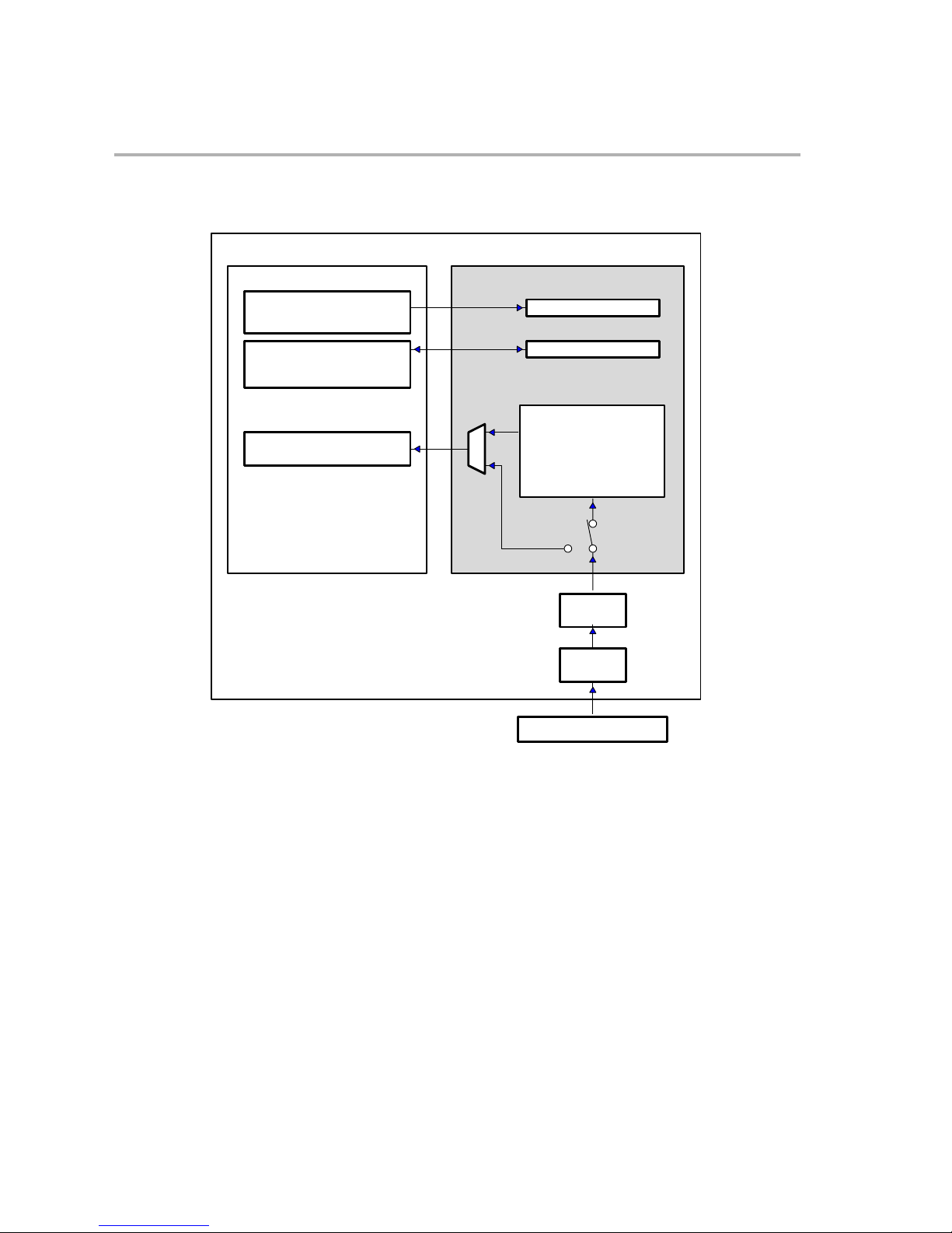
1 Introduction
Instruction Cache
On the TMS320VC5501/5502 digital signal processors (DSPs), instructions
can reside in internal memory or external memory. When instructions reside
in external memory, the instruction cache (I-Cache) can improve the overall
system performance by buffering the most recent instructions accessed by the
central processing unit (CPU).
Figure 1 shows how the I-Cache fits into the DSP system. CPU status register
ST3_55 contains three cache-control bits for enabling, freezing, and flushing
the I-Cache (see section 2 on page 16). To configure the I-Cache and check
its status, the CPU accesses a set of registers in the I-Cache. For storing
instructions, the I-Cache contains one 2-way cache. The 2-way cache uses
2-way set associative mapping and holds up to 16K bytes: 512 sets, two lines
per set, four 32-bit words per line. In the 2-way cache, each line is identified
by a unique tag.
9Instruction CacheSPRU630C
Page 10
Introduction
Figure 1. Conceptual Block Diagram of the I-Cache in the DSP System
VC5501/5502 DSP
CPU
Cache-control bits in
ST3_55 to enable, freeze,
and flush I-Cache
Data read/write logic
to configure and
monitor I-Cache
Instruction buffer
queue
I-Cache
Control logic
I-Cache registers
2-way cache
I-Cache
disabled
IPORT
EMIF
External memory
I-Cache
enabled
When fetching instruction code from external memory, the CPU sends a 32−bit
access request to the instruction cache (I-Cache) using its program−read data
bus (P bus). If the instruction cache is disabled, the request goes directly to
the IPORT and then to the external memory interface (EMIF). The EMIF must
read 32 bits from the external memory and then pass all 32 bits to the IPORT,
which in turn sends the data to the CPU.
Two things could happen if the instruction cache is enabled. In the case of a
cache hit, the CPU request will be immediately serviced by the instruction
cache and no data will be read from external memory. In the case of a cache
miss, the instruction cache will request four 32−bit words from the EMIF
through the IPORT. The EMIF will read four 32−bit words from external
memory and then pass the data to the instruction cache through the IPORT.
The instruction cache will then send the requested data to the CPU and update
its memory contents. More information on the EMIF can be found in the
Instruction Cache10 SPRU630C
Page 11

TMS320VC5501/5502 DSP External Memory Interface (EMIF) Reference
Guide ( literature number SPRU621).
Since data from the EMIF passes through the IPORT to get to the I−cache, the
IPORT must be properly enabled to allow proper cache operation. The IPORTI
bit in the Idle Control Register (ICR) controls whether the IPORT is enabled
or disabled after an idle instruction. The IPORT is enabled by default after
reset. The IPORT should not be disabled while the cache is in use. For detailed
information about the ICR, see the data manual for the DSP being used.
Note:
The I-Cache does not automatically maintain coherency. If you write to a
location in program memory, the corresponding line in the I-Cache is not
updated. To regain coherency you must flush the I-Cache as described in
section 2.2 (page 16).
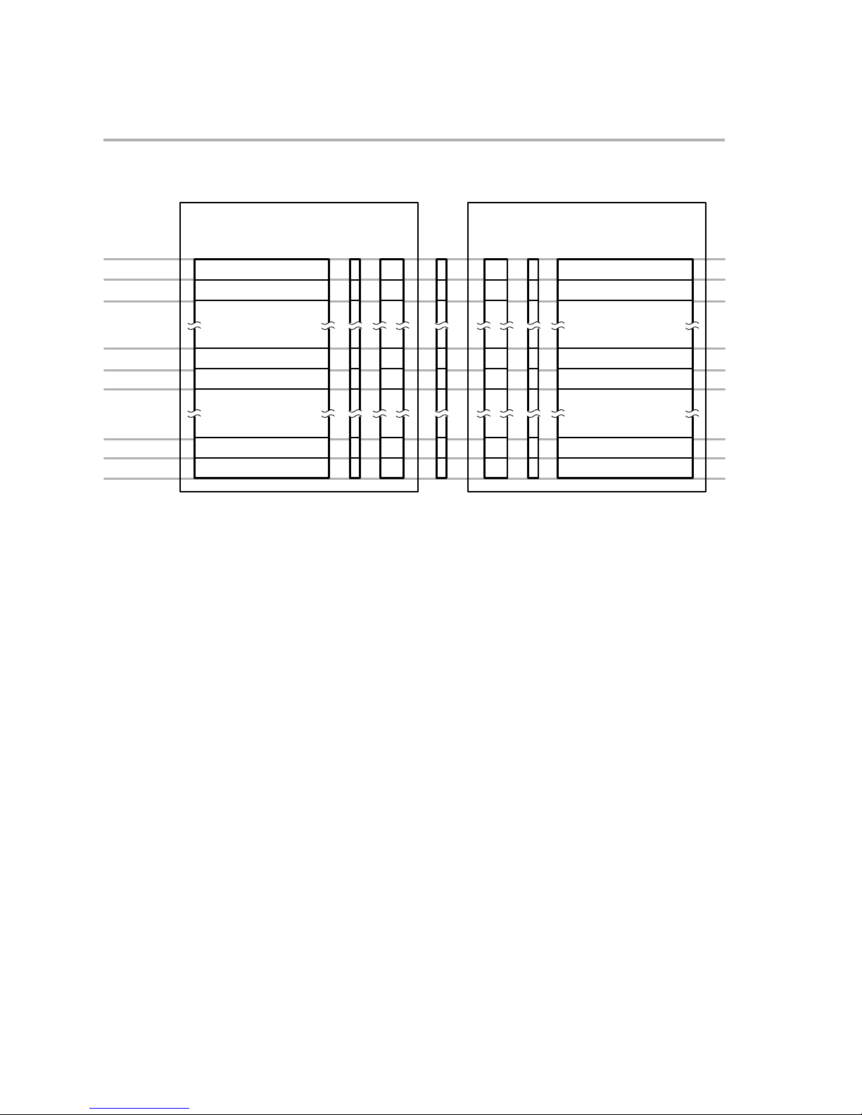
1.1 2-Way Cache
Introduction
As shown in Figure 2, the 2-way cache has two memory banks. Each memory
bank has the same parts:
- Data array. Each data array contains 512 lines (0 through 511) that the
I-Cache can fill one by one in response to misses in the 2-way cache.
- Line valid (LV) bit array. Each line has a line valid bit. Once a line has been
loaded, its line valid bit is set. Whenever the I-Cache is flushed, all 512 line
valid bits are cleared, invalidating all the lines. For more information on
flushing the I-Cache, see section 2.2 on page 16.
- Tag array. Each line has a tag field. When the I-Cache receives a 24-bit
fetch address from the CPU, the I-Cache interprets bits 23−13 as a tag.
When a line gets filled, the associated tag is stored in the tag field for that
line.
Across the two memory banks, every two lines with the same number belong
to one set. For example, line 0 of memory bank 1 and line 0 of memory bank
2 belong to set 0. When the I-Cache receives a fetch address, the I-Cache
finds the set number in bits 12−4. If the I-Cache must replace one of the lines
in the set, it uses a least-recently used (LRU) algorithm: The line replaced is
the one that has been unused for the longest time. Each set has an LRU bit
that is toggled to indicate which line should be replaced.
11Instruction CacheSPRU630C
Page 12
Introduction
Figure 2. 2-Way Cache
Memory bank 1 Memory bank 2
Set 0
Set 1
.
.
.
Set 254
Set 255
.
.
.
Line 0
Line 1
.
.
.
Line 254
Line 255
.
.
.
DataLVTa gLRUTa gLVData
Line 0
Line 1
.
.
.
Line 254
Line 255
.
.
.
Set 510
Set 511
Line 510
Line 511
1.2 I-Cache Operation
When the 5501/5502 CPU requests instructions, it requests 32 bits at a time.
With each request, the CPU sends a fetch address that indicates where to read
the 32 bit requested word. When a fetch request arrives, the I-Cache performs
an instruction presence check; that is, it determines whether the requested
word is available in the 2-way cache.
Section 1.2.2 describes the steps of the instruction presence check and
explains the factors that determine whether the I-Cache fetches the requested
word from the 2-way cache, or from external memory.
Line 510
Line 511
Instruction Cache12 SPRU630C
Page 13
Introduction
1.2.1 How the I-Cache Uses the Fetch Address
Figure 3 and Table 1 describe how the I-Cache uses the fetch address for the
2-way cache.
Figure 3. Fetch Address Fields for the 2-Way Cache
23 13 12 4 3 2 1 0
Ta g
11 bits 9 bits 2 bits 2 bits
Index (set) Offset Byte
Table 1. Fetch Address Field Descriptions for the 2-Way Cache
Bit Field Description
23−13 Tag Whenever a line of the 2-way cache is loaded from external memory, the tag
portion of the fetch address is stored with the line (in the tag array). During an
instruction presence check, the I-Cache uses the Index field to find the
addressed set and then compares both tags in the set with the tag portion of the
fetch address.
12−4 Index This 9-bit value references one of the 512 sets of the 2-way cache. As shown in
Figure 2 (page 12), each set has two lines.
3−2 Offset When the I-Cache must read a 32-bit word from one of the lines of the 2-way
cache, the offset field indicates which of the four 32-bit words in the line should
be read.
1−0
Byte This field is not used by the I-Cache but is the part of the fetch address that
indicates the specific byte being addressed.
1.2.2 Instruction Presence Check and the Corresponding I-Cache Response
As mentioned earlier, when a fetch request arrives, the I-Cache performs an
instruction presence check to determine whether the 32-bit requested word is
available in the I-Cache. During the instruction presence check, the I-Cache
performs these two operations on the 2-way cache:
1) Compares the tag portion of the fetch address with the tag in the data array
at the location referenced by the Index portion of the fetch address.
2) Checks the line valid bit at the referenced location, to determine whether
the line associated with the tag is valid.
If the tag comparison fails and/or the line valid bit is 0, this qualifies as a miss.
If the instruction presence check finds a tag match and the line valid bit is 1,
this qualifies as a hit. Table 2 summarizes the possible presence check and
the corresponding I-Cache responses. Whenever a line in the I-Cache must
be loaded from external memory the I-Cache uses the line load process
described in section 1.2.3.
13Instruction CacheSPRU630C
Page 14

Introduction
Table 2. Instruction Presence Check and I-Cache Response
Case 2-Way Cache Presence I-Cache Response
1 Miss False 2-way cache line loaded from external memory,
requested 32-bit word delivered to CPU
2 Hit True Requested 32-bit word taken directly from 2-way cache
1.2.3 Line Load Process
When an instruction presence check results in a fetch from the external
memory, the 4-word external memory block that contains the requested word
is fetched and loaded into a line in the I-Cache. This line load process is
illustrated in Figure 4. The I-Cache uses the external memory interface (EMIF)
to fetch the 4-word block that contains the requested word. These four 32-bit
words are written to the line in the I-Cache one word at a time. The I-Cache
delivers the requested word to the CPU as soon as the word arrives in the data
array, even if the rest of the line is still being loaded. When the entire line is
loaded in the data array, the corresponding tag is written to the tag array and
the line valid bit is set to validate the line.
Instruction Cache14 SPRU630C
Page 15

Figure 4. Flow Chart of the Line Load Process
I-Cache must load
2-way cache line
Command EMIF to read
four 32-bit words from
external memory
Introduction
Is
word
received
?
Yes
Write word to line
Is
it the
requested
word
?
Yes
Deliver word to
I unit of CPU
No
No
Line
load done
?
Yes
End
Wait for
next word
No
15Instruction CacheSPRU630C
Page 16

CPU Bits for Controlling the I-Cache
2 CPU Bits for Controlling the I-Cache
Control of the I-Cache is maintained not only through the I-Cache registers but
also through three bits located in status register ST3_55 of the CPU. These
bits are highlighted in Figure 5. For more details about ST3_55, see the
TMS320C55x DSP CPU Reference Guide (SPRU371).
Figure 5. CAFRZ, CAEN, and CACLR Bits in ST3_55
15 14 13 12 11 8
CAFRZ CAEN CACLR HINT Reserved
R/W-0 R/W-0 R/W-0
76543210
CBERR
2.1 CAEN Bit to Enable or Disable the I-Cache
MPNMC SATA Reserved CLKOFF SMUL SST
To enable the I-Cache, set the cache enable (CAEN) bit of ST3_55. To disable
the I-Cache, clear the CAEN bit. When disabled, the lines of the I-Cache data
arrays are not checked; instead, the I-Cache forwards instruction-fetch
requests directly to the external memory interface (EMIF).
For proper operation of the I-Cache, configure the I-Cache before enabling it
and disable the I-Cache before making any changes to its configuration.
A DSP reset forces CAEN = 0 (I-Cache disabled).
2.2 CACLR Bit to Flush the I-Cache
The flush operation is defined as the invalidation of all of the lines in the
I-Cache.
To flush the I-Cache, write 1 to the cache clear (CACLR) bit of ST3_55. In
response, all the line valid bits of the 2-way cache are cleared. The CACLR
bit remains 1 until the flush process is complete, at which time CACLR is
automatically reset to 0.
A DSP reset forces CACLR = 0 (no flush in process).
Instruction Cache16 SPRU630C
Page 17

CPU Bits for Controlling the I-Cache
2.3 CAFRZ Bit to Freeze the Contents of the I-Cache
When you write 1 to the cache freeze (CAFRZ) bit of ST3_55, the contents of
the I-Cache are locked. Instruction words that were cached prior to the freeze
are still accessible in the case of an I-Cache hit, but the data arrays are not
updated in response to an I-Cache miss. To re-enable updates, write 0 to
CAFRZ.
A DSP reset forces CAFRZ = 0 (I-Cache not frozen).
Note:
When the I-Cache is frozen (CAFRZ = 1), each I-Cache miss still causes a
4-word (16-byte) fetch cycle in the EMIF. It is recommended that you profile
your code to minimize the number of misses during an I-Cache freeze.
17Instruction CacheSPRU630C
Page 18

Configuring and Enabling the I-Cache
3 Configuring and Enabling the I-Cache
This section gives the procedures for preparing and enabling the I-Cache.
The I-Cache registers mentioned in this section are described in section 6
(page 22). The cache enable (CAEN) bit that is used to enable and disable the
I-Cache is described in section 2.1 (page 16).
Note:
Write to the control registers (ICGC and ICWC) only when the I-Cache is
disabled (CAEN = 0 in ST3_55).
To initialize the I-Cache, write CE3Ch to ICGC. Then set the cache enable bit
(CAEN) of the CPU status register ST3_55 to send an enable request to the
I-Cache.
Instruction Cache18 SPRU630C
Page 19

4 Timing Considerations
As the I-Cache fetches and returns 32-bit words requested by the CPU, two
key time periods affect the speed of the I-Cache:
- Hit time
- Miss penalty
4.1 Hit Time
The hit time is the time required for the I-Cache to deliver the 32-bit requested
word to the CPU in the case of a hit (when the word is present in the I-Cache).
The hit time is either 1 or 2 CPU clock cycles:
- An initial request (a request that follows a period of inactivity) has a hit
time of 2 cycles.
- Subsequent requests have a hit time of 1 cycle if:
J The requests are consecutive (no inactivity in between) and
J The requests are to sequential addresses
Timing Considerations
- Subsequent requests have a hit time of 2 cycles if:
J The requests are not consecutive or
J The requests are to nonsequential addresses
19Instruction CacheSPRU630C
Page 20

Timing Considerations
4.2 Miss Penalty
The miss penalty is the time required for the I-Cache to deliver the 32-bit
requested word to the CPU in the case of a miss (when the word must be
fetched from external memory). In response to a miss, the I-Cache requests
four words from the external memory interface (EMIF) to load the appropriate
line.
The miss penalty due to an initial request to the EMIF is:
1) Four cycles for the I-Cache to receive the fetch request, detect an I-Cache
2) X cycles for the EMIF to get the requested word to the I-Cache, where X
miss, and forward the fetch request to the EMIF.
depends on factors such as:
- The initial access latency of the type of external memory that is used
- The position of the requested word in the I-Cache line. For example, if
the requested word is the third word of the line, two words are fetched
before the requested word.
- Whether the four words are fetched in a burst access (if synchronous
memory is used)
3) Three cycles for the I-Cache to get the requested 32-bit word to the
instruction fetch unit (I unit) of the CPU.
Subsequent requests can incur a smaller miss penalty if the external memory
is synchronous. After accessing the first word from synchronous memory, the
EMIF can return each of the remaining words in a single cycle.
The I-Cache includes a feature that reduces miss penalties overall. As
mentioned earlier, the I-Cache gives the requested word to the CPU as soon
as it arrives in the I-Cache line, rather than after the whole line is loaded.
Instruction Cache20 SPRU630C
Page 21

Power, Emulation, and Reset Considerations
5 Power, Emulation, and Reset Considerations
See the TMS320C5501 Fixed-Point Digital Signal Processor Data Manual
(SPRS206) or the TMS320C5502 Fixed-Point Digital Signal Processor Data
Manual (SPRS166) for information on power and reset.
5.1 Emulator Access
The software emulator can read the contents of the I-Cache during the debug
mode. The contents of the I-Cache are not modified by emulator read
operations.
5.2 Effect of Setting a Software Breakpoint
During emulation, If you set or remove a software breakpoint at an instruction,
the corresponding line in the I-Cache is automatically invalidated.
5.3 Reconfiguration Required After a DSP Reset
After a DSP reset, the I-Cache is not automatically reconfigured for use. Make
sure that your initialization code configures the I-Cache as described in
section 3 (page 18) after every reset.
21Instruction CacheSPRU630C
Page 22

I-Cache Registers
6 I-Cache Registers
Control of the I-Cache is maintained through a set of registers within the
I-Cache. These registers are accessible at addresses in the I/O space of the
DSP. For the addresses, see the TMS320C5501 Fixed-Point Digital Signal
Processor Data Manual (SPRS206) or the TMS320C5502 Fixed-Point Digital
Signal Processor Data Manual (SPRS166).
Table 3. Summary of the I-Cache Registers
Name Description See ...
ICGC Global control register Page 22
ICFARL Flush line low address register Page 24
ICFARH Flush line high address register Page 24
ICWMC
Way miss-counter register Page 25
6.1 Global Control Register (ICGC)
The TMS320C5501/5502 I-Cache supports one 2-way cache. Before
enabling the I-Cache, use the global control register (ICGC) to initialize it.
You can write two legal values to ICGC:
- CE3Ch to initialize the I-Cache
- DE3Ch to force a line flush
Do not write other values to this register. A DSP reset invalidates the content
of ICGC. Make sure your initialization code writes CE3Ch to ICGC after every
reset.
Figure 6. I-Cache Global Control Register (ICGC)
15 13 12 11 0
Reserved
R-110 R/W-0 R/W-011000111100
Legend: R = Read; W = Write; -n = Value after reset
FLUSHLINE Reserved
Instruction Cache22 SPRU630C
Page 23

Table 4. I-Cache Global Control Register (ICGC) Bits
Bit Field Description
15−13 Reserved Always write 110b to these reserved bits.
12 FLUSHLINE Flush the cache line specified by the flush line address registers
(ICFARH and ICFARL). The line flush starts when a 1 is written to the
FLUSHLINE bit. The I-cache clears this bit to 0 when the line flush is
completed. Line flushes can be performed only when the I-cache is
enabled.
I-Cache Registers
11−0
Reserved Always write E3Ch to these reserved bits.
A line flush invalidates the line valid (LV) bit for a specific line in the cache. The
address associated with the line to be flushed is contained in the flush line
address registers (ICFARL and ICFARH). ICFARL contains the least
significant 16 bits of the address associated with the line to be flushed.
ICFARH contains the most significant 8 bits of the address associated with the
line to be flushed. The address specified in these registers is a byte address.
See section 6.2 on page 24 for information about ICFARH and ICFARL.
To flush a cache line associated with a specific program memory address,
perform the following steps:
Step 1: Write the least-significant 16 bits of the address to ICFARL.
Step 2: Write the most-significant 8 bits of the address to ICFARH. The
upper 8 bit of ICFARH should be written as zeroes.
Step 3: Write the value DE3Ch to ICGC to initiate a line flush.
Step 4: When the line flush is complete, the FLUSHLINE bit is automatically
cleared.
23Instruction CacheSPRU630C
Page 24

I-Cache Registers
6.2 Flush Line Address Registers (ICFARL and ICFARH)
The flush line address registers (ICFARL and ICFARH) contain the program
address that is used to determine the line to be flushed. When a line flush is
initiated (DE3Ch written to ICGC), the I-Cache automatically flushes the line
associated with the program address contained in these registers.
Figure 7. I-Cache Flush Line Low Address Register (ICFARL)
15 0
LAL[15:0]
R/W-0
Table 5. I-Cache Flush Line Low Address Register (ICFARL) Bits
Bit Field Description
15−0 LAL Least-significant 16 bits of the program address associated with the line to
be flushed.
Figure 8. I-Cache Flush Line High Address Register (ICFARH)
15 8 7 0
Reserved
R-0 R/W-0
LAH[7:0]
Table 6. I-Cache Flush Line High Address Register (ICFARH) Bits
Bit Field Description
15−8 Reserved These reserved bits should be written as 0s.
7−0 LAH Most-significant 8 bits of the program address associated with the line to
be flushed.
Instruction Cache24 SPRU630C
Page 25

I-Cache Registers
6.3 Way Miss Counter Register (ICWMC)
The ICWMC is incremented by 1 for every miss in the 2-way cache. A DSP
reset forces ICWMC = 0000h. ICWMC can be loaded with a value in the range
0000h − FFFFh. When ICWMC is read, it is reset to 0000h. When it reaches
FFFFh, the incrementing stops and ICWMC holds the value FFFFh until the
register is read or loaded with a different value. Your program can read the
value and write that value.
Figure 9. I-Cache Way Miss-Counter Register (ICWMC)
15 0
MISSCNT
R/W−0
Legend: R = Read; W = Write; -n = Value after reset; -x = Value after reset is not defined
Table 7. I-Cache Way Miss Counter Register (ICWMC) Bits
Bit Field Description
15−0 MISSCNT A counter to count the number of mis-compares for the 2-way cache. This
field can be preset by a write to the register from the CPU. The counter
stops at the upper count limit (FFFFh). If read by the CPU, the counter will
reset.
25Instruction CacheSPRU630C
Page 26

This page is intentionally left blank.
Instruction Cache26 SPRU630C
Page 27

Revision History
This document was revised to SPRU630C from SPRU630B, which was
released in August 2003. Changes that were made since the last revision are
listed in the following table.
Page Additions/Modifications/Deletions
10
10 and 11
13
Added IPORT block to Figure 1.
Revised paragraphs 2 − 4 in Section 1.
Added bit number 12 in Figure 3.
27Instruction CacheSPRU630C
Page 28

This page is intentionally left blank.
Instruction Cache28 SPRU630C
Page 29

Index
Index
2−way cache, 11
B
block diagram of I−Cache, 10
C
cache clear bit (CACLR)
described, 16
shown in figure, 16
cache control bits of CPU, 16
cache enable bit (CAEN)
described, 16
shown in figure, 16
cache freeze bit (CAFRZ)
described, 17
shown in figure, 16
CACLR bit
described, 16
shown in figure, 16
CAEN bit
described, 16
shown in figure, 16
CAFRZ bit
described, 17
shown in figure, 16
conceptual block diagram of I−Cache, 10
configure I−Cache, 18
CPU bits for controlling I−Cache, 16
E
emulator access, 21
enable I−Cache
as part of initialization procedure, 18
CAEN bit description, 16
external memory interface EMIF, 10
F
fetch address, how I−Cache uses, 13
flush I−Cache, 16
flush line address registers (ICFARL and ICFARH),
24
FLUSHLINE bit of ICGC
described in table, 23
shown in figure, 22
force a line flush, 22
freeze contents of I−Cache, 17
G
global control register (ICGC), 22
H
hit, 13
hit time, 19
how I−Cache uses fetch address, 13
D
data array, 11
diagram of I−Cache, 10
disable I−Cache, 16
DSP reset, reconfiguring I−Cache after, 21
I
ICFARL and ICFARH, 24
ICGC, 22
ICWMC, 25
initialize I−Cache, 22
initiate a line flush, 23
29
Page 30

Index
instruction cache (I-Cache), 10
instruction presence check, 13
introduction to I−Cache, 9
IPORT, 10
L
LAH bits of ICFARH
described in table, 24
shown in figure, 24
LAL bits of ICFARL
described in table, 24
shown in figure, 24
least−recently used (LRU) algorithm, 11
line flush, 23
line load process, 14
line valid (LV) bit array, 11
LRU algorithm, 11
M
memory banks, 11
miss, 13
miss penalty, 20
MISSCNT bits of ICWMC
described in table, 25
shown in figure, 25
O
operation of I−Cache, 12
P
presence check, 13
R
reconfiguration of I−Cache after DSP reset, 21
registers of I−Cache, 22
S
software breakpoint, effect on I−Cache, 21
status register ST3_55 of CPU, 16
synchronous memory miss penalty, 20
T
tag array, 11
timing considerations, 19
W
way miss counter register (ICWMC), 25
30
 Loading...