

Page 1

现货库存、技术资料、百科信息、热点资讯,精彩尽在鼎好!
TMS320VC5420
FIXED-POINT DIGITAL SIGNAL PROCESSOR
SPRS080C – MARCH 1999 – REVISED APRIL 2000
200-MIPS Dual-Core DSP Consisting of Two
Independent Subsystems
Each Core Has an Advanced Multibus
Architecture With Three Separate 16-Bit
Data Memory Buses and One Program Bus
40-Bit Arithmetic Logic Unit (ALU)
Including a 40-Bit Barrel-Shifter and Two
40-Bit Accumulators Per Core
Each Core Has a 17- × 17-Bit Parallel
Multiplier Coupled to a 40-Bit Adder for
Non-Pipelined Single-Cycle Multiply/
Accumulate (MAC) Operations
Each Core Has a Compare, Select, and
Store Unit (CSSU) for the Add/Compare
Selection of the Viterbi Operator
Each Core Has an Exponent Encoder to
Compute an Exponent Value of a 40-Bit
Accumulator Value in a Single Cycle
Each Core Has Two Address Generators
With Eight Auxiliary Registers and Two
Auxiliary Register Arithmetic Units
(ARAUs)
16-Bit Data Bus With Data Bus Holder
Feature
256K × 16 Extended Program Address
Space
Total of 200K × 16 Dual- and Single-Access
On-Chip RAM
Single-Instruction Repeat and
Block-Repeat Operations
Instructions With 32-Bit Long Word
Operands
Instructions With 2 or 3 Operand Reads
Fast Return From Interrupts
NOTE:This data sheet is designed to be used in conjunction with the
(literature number SPRU307).
Arithmetic Instructions With Parallel Store
and Parallel Load
Conditional Store Instructions
Output Control of CLKOUT
Output Control of TOUT
Power Consumption Control With IDLE1,
IDLE2, and IDLE3 Instructions
Dual 1.8-V (Core) and 3.3-V (I/O) Power
Supplies for Low Power, Fast Operation
10-ns Single-Cycle Fixed-Point Instruction
Execution
Interprocessor Communication via Two
Internal 8-Element FIFOs
12 Channels of Direct Memory Access
(DMA) for Data Transfers With No CPU
Loading (6 Channels Per Subsystem)
Six Multichannel Buffered Serial Ports
(McBSPs) (Three McBSPs Per Subsystem)
16-Bit Host-Port Interface (HPI16)
Multiplexed With External Memory Interface
Pins
Software-Programmable Phase-Locked
Loop (PLL) Provides Several Clocking
Options (Requires External TTL Oscillator)
On-Chip Scan-Based Emulation Logic
T wo Software-Programmable Timers
(One Per Subsystem)
Software-Programmable Wait-State
Generator (14 Wait States Maximum)
Provided in 144-pin BGA Ball Grid Array
(GGU Suffix) and 144-pin Thin Quad
Flatpack (TQFP) (PGE Suffix) packages
TMS320C5000 DSP Family Functional Overview
Please be aware that an important notice concerning availability, standard warranty, and use in critical applications of
Texas Instruments semiconductor products and disclaimers thereto appears at the end of this data sheet.
PRODUCTION DATA information is current as of publication date.
Products conform to specifications per the terms of Texas Instruments
standard warranty. Production processing does not necessarily include
testing of all parameters.
POST OFFICE BOX 1443 • HOUSTON, TEXAS 77251–1443
Copyright 2000, Texas Instruments Incorporated
1
Page 2

TMS320VC5420
FIXED-POINT DIGITAL SIGNAL PROCESSOR
SPRS080C – MARCH 1999 – REVISED APRIL 2000
Table of Contents
Pin Assignments 5. . . . . . . . . . . . . . . . . . . . . . . . . . . . . . . . . .
Signal Descriptions 9. . . . . . . . . . . . . . . . . . . . . . . . . . . . . . . .
Functional Overview 15. . . . . . . . . . . . . . . . . . . . . . . . . . . . . .
Memory 16. . . . . . . . . . . . . . . . . . . . . . . . . . . . . . . . . . . . . . . . .
Multicore Reset Signals 18. . . . . . . . . . . . . . . . . . . . . . . . . . .
On-Chip Peripherals 20. . . . . . . . . . . . . . . . . . . . . . . . . . . . . .
16-bit Host-Port Interface (HPI16) 23. . . . . . . . . . . . . . . . . .
Multichannel Buffered Serial Port (McBSP) 25. . . . . . . . . . .
Direct Memory Access Unit (DMA) 26. . . . . . . . . . . . . . . . . .
Subsystem Communications 28. . . . . . . . . . . . . . . . . . . . . . .
General-Purpose I/O 29. . . . . . . . . . . . . . . . . . . . . . . . . . . . . .
Memory-Mapped Registers 32. . . . . . . . . . . . . . . . . . . . . . . .
Interrupts 36. . . . . . . . . . . . . . . . . . . . . . . . . . . . . . . . . . . . . . . .
IDLE3 Power-Down Mode 38. . . . . . . . . . . . . . . . . . . . . . . . .
Emulating the ’5420 Device 38. . . . . . . . . . . . . . . . . . . . . . . .
Documentation Support 39. . . . . . . . . . . . . . . . . . . . . . . . . . .
Absolute Maximum Ratings 40. . . . . . . . . . . . . . . . . . . . . . . .
Recommended Operating Conditions 40. . . . . . . . . . . . . . .
Electrical Characteristics 41. . . . . . . . . . . . . . . . . . . . . . . . . .
External Multiply-By-N ClockOption 42. . . . . . . . . . . . . . . . .
Bypass Option 43. . . . . . . . . . . . . . . . . . . . . . . . . . . . . . . . . . .
External Memory Interface Timing 44. . . . . . . . . . . . . . . . . .
Ready Timing 48. . . . . . . . . . . . . . . . . . . . . . . . . . . . . . . . . . . .
Parallel I/O Interface Timing 50. . . . . . . . . . . . . . . . . . . . . . .
Reset, BIO, Interrupt, and XIO Timing 54. . . . . . . . . . . . . . .
External Flag (XF), and Timer Output (TOUT) Timing 56. .
General Purpose Input Output (GPIO) Timing 57. . . . . . . .
SELA/B Timing 58. . . . . . . . . . . . . . . . . . . . . . . . . . . . . . . . . . .
Multichannel Buffered Serial Port Timing 59. . . . . . . . . . . . .
multichannel buffered serial port timing (continued) 60. . . .
HPI16 Timing 67. . . . . . . . . . . . . . . . . . . . . . . . . . . . . . . . . . . .
Mechanical Data 75. . . . . . . . . . . . . . . . . . . . . . . . . . . . . . . . .
description
The TMS320VC5420 fixed-point digital signal processor (DSP) is a dual CPU device capable of up to 200-MIPS
performance. The ’5420 consists of two independent ’54x subsystems capable of core-to-core
communications.
Each subsystem CPU is based on an advanced, modified Harvard architecture that has one program memory
bus and three data memory buses. The processor also provides an arithmetic logic unit (ALU) that has a high
degree of parallelism, application-specific hardware logic, on-chip memory , and additional on-chip peripherals.
Each subsystem has separate program and data spaces, allowing simultaneous accesses to program
instructions and data. Two read operations and one write operation can be performed in one cycle. Instructions
with parallel store and application-specific instructions can fully utilize this architecture. Furthermore, data can
be transferred between program and data spaces. Such parallelism supports a powerful set of arithmetic, logic,
and bit manipulation operations that can be performed in a single machine cycle. In addition, the ’5420 includes
the control mechanisms to manage interrupts, repeated operations, and function calls.
The ’5420 is offered in two temperature ranges and individual part numbers as shown below . (Please note that
the industrial temperature device part numbers do not follow the typical numbering tradition.)
Commercial temperature devices (0°C to 85°C)
TMS320VC5420PGE200 (144-pin LQFP)
TMS320VC5420GGU200 (144-pin BGA)
Industrial temperature range devices (–40°C to 100°C)
TMS320C5420PGEA200 (144-pin LQFP)
TMS320C5420GGUA200 (144-pin BGA)
2
POST OFFICE BOX 1443 • HOUSTON, TEXAS 77251–1443
Page 3

TMS320VC5420
FIXED-POINT DIGITAL SIGNAL PROCESSOR
SPRS080C – MARCH 1999 – REVISED APRIL 2000
PPD7
PPA8
PPA0
DV
DD
PPA9
PPD1
A_INT1
A_NMI
IOSTRB
A_GPIO2/BIO
A_GPIO1
A_RS
A_GPIO0
V
SS
V
SS
CV
DD
A_BFSR1
A_BDR1
A_BCLKR1
A_BFSX1
CV
DD
V
SS
A_BDX1
A_BCLKX1
A_XF
A_CLKOUT
VCO
TCK
TMS
TDI
TRST
EMU1/OFF
DV
DD
A_INT0
EMU0
TDO
TMS320VC5420 PGE PACKAGE
†‡§
(TOP VIEW)
DD
SS
PPD4
PPD0
PPD5
PPD6
A_BFSX2
141
140
A_BDX2
139
138
V
144
143
142
1
2
3
4
5
6
7
8
9
10
11
12
13
14
15
16
17
18
19
20
21
22
23
24
25
26
27
28
29
30
31
32
33
34
35
36
373839404142434445464748495051525354555657585960616263646566676869
A_BFSR2
A_BDR2
A_BCLKR2
137
136
135
SS
V
134
A_BCLKX2
CV
133
132
DD
READY
131DV130
NC
CLKIN
129
128
SSA
V
127
AV
126
DD
V
SS
125
B_BCLKX2
124
B_BDX2
B_BFSX2
B_BCLKR2
123
122
121
CV
120
DD
SS
V
119
B_BDR2
B_BFSR2
118
117
PPD2
PPD3
116
115
DD
PPA1
PPA5
114
113
DV
112
PPA6
PPA4
111
110
707172
PPA7
109
108
107
106
105
104
103
102
101
100
PPA14
PPA15
V
PPA16
PPA17
B_INT0
B_INT1
B_NMI
IS
99
B_GPIO2/BIO
98
B_GPIO1
97
B_GPIO0
96
B_BFSR1
95
B_BDR1
94
CV
93
V
92
B_BCLKR1
91
B_BFSX1
90
V
89
B_BDX1
88
B_BCLKX1
87
CV
86
V
85
TEST
84
XIO
83
B_RS
82
B_XF
B_CLKOUT
81
HMODE
80
HPIRS
79
PPA13
78
PPA12
77
V
76
DV
75
PPA11
74
PPA10
73
SS
DD
SS
SS
DD
SS
SS
DD
PS
MSTRB
A_BDX0
A_BCLKX0
DS
B_BCLKX0
SS
V
V
PPD15
PPD14SSPPD13
PPD12
A_BFSR0
†
NC = No internal connection
‡
DVDD is the power supply for the I/O pins while CVDD is the power supply for the core CPU. VSS is the ground for both the I/O
pins and the core CPU.
§
Pin configuration shown for nonmultiplexed mode only. See the Pin Assignments for the TMS320VC5420PGE table for multiplexed
A_BDR0
A_BFSX0
A_BCLKR0
SS
DD
V
CV
DD
V
DV
B_BDX0
SS
B_BFSX0
SS
DD
V
CV
B_BDR0
B_BCLKR0
R/W
PPA2
B_BFSR0
PPA3
PPD8
SELA/B
PPD9
PPD10
SS
V
PPD11
functions of specific pins.
POST OFFICE BOX 1443 • HOUSTON, TEXAS 77251–1443
3
Page 4
TMS320VC5420
FIXED-POINT DIGITAL SIGNAL PROCESSOR
SPRS080C – MARCH 1999 – REVISED APRIL 2000
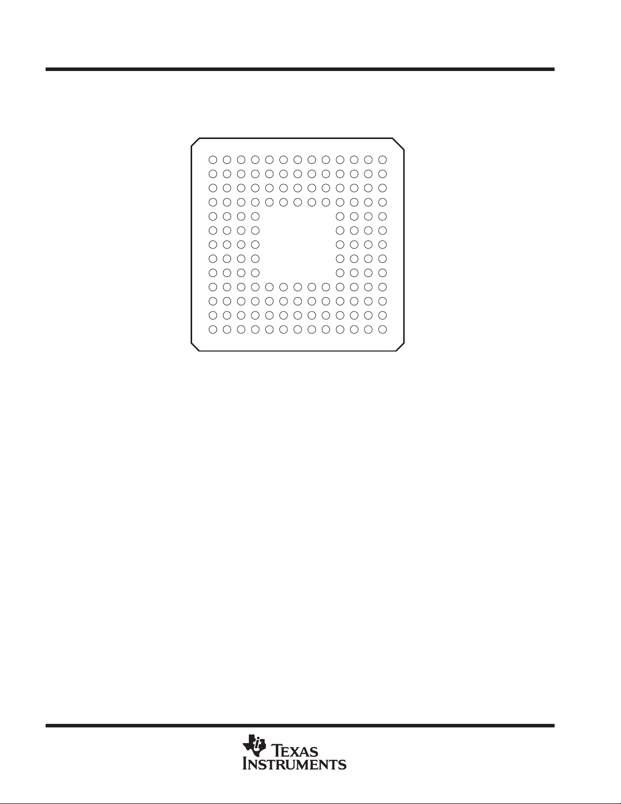
TMS320VC5420 GGU PACKAGE
(BOTTOM VIEW)
12
3456781012 1113 9
A
B
C
D
E
F
G
H
J
K
L
M
N
The pin assignments table for the TMS320VC5420GGU lists each pin name and its associated pin number for
this 144-pin ball grid array (BGA) package.
4
POST OFFICE BOX 1443 • HOUSTON, TEXAS 77251–1443
Page 5
TMS320VC5420
FIXED-POINT DIGITAL SIGNAL PROCESSOR
SPRS080C – MARCH 1999 – REVISED APRIL 2000
pin assignments
The ’5420 pin assignments tables list each pin name and corresponding pin number for the two package types.
Some of the ’5420 pins can be configured for one of two functions. For these pins, the primary pin name is listed
in the primary column. The secondary pin name is listed in the secondary column and is shaded grey.
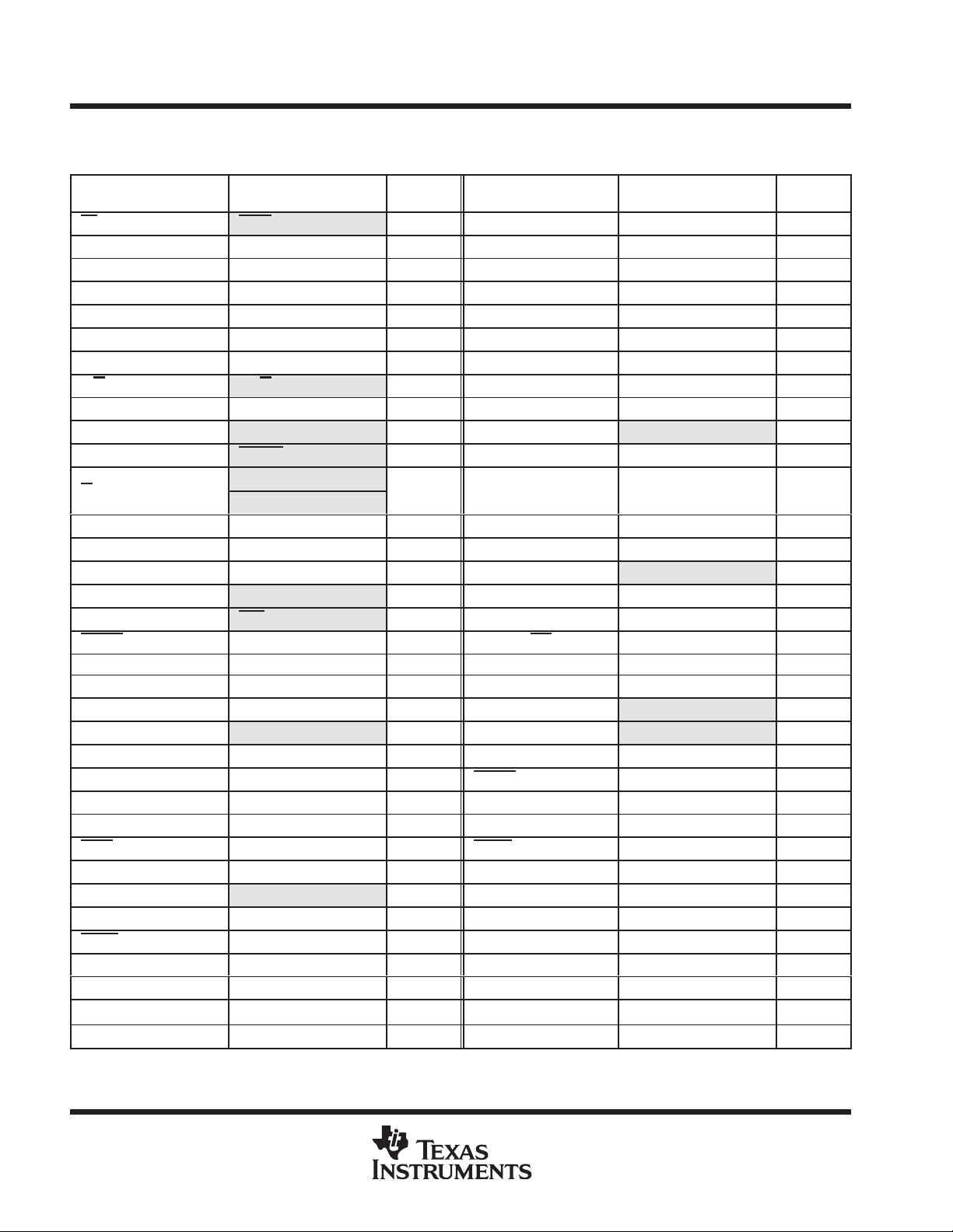
Pin Assignments for the TMS320VC5420PGE
(144-Pin Thin Quad Flatpack)
PRIMARY
SIGNAL NAME
PPD7 HD7 1 PPA8
PPA0 A_HINT 3 DV
PPA9 5 PPD1 HD1 6
A_INT1 7 A_NMI 8
IOSTRB
A_GPIO1 11 A_RS 12
A_GPIO0 13 V
V
SS
A_BFSR1 17 A_BDR1 18
A_BCLKR1 19 A_BFSX1 20
CV
DD
A_BDX1 23 A_BCLKX1 24
A_XF 25 A_CLKOUT 26
VCO 27 TCK 28
TMS 29 TDI 30
TRST 31 EMU1 32
DV
DD
EMU0 35 TDO 36
V
SS
PPD14 HD14 39 V
PPD13 HD13 41 PPD12 HD12 42
A_BFSR0 43 A_BDR0 44
A_BCLKR0 45 A_BFSX0 46
V
SS
A_BDX0 49 A_BCLKX0 50
MSTRB HCS 51 DS HDS2 52
PS HDS1 53 B_BCLKX0 54
B_BDX0 55 DV
V
SS
B_BCLKR0 59 B_BDR0 60
CV
DD
B_BFSR0 63 R/W HR/W 64
PPA2 HCNTL1 65 PPA3 HCNTL0 66
SELA/B 67 PPD8 HD8 68
PPD9 HD9 69 PPD10 HD10 70
PPD11 HD11 71 V
SECONDARY
SIGNAL NAME
A_GPIO3
A_TOUT
PIN
NO.
9 A_GPIO2/BIO 10
15 CV
21 V
33 A_INT0 34
37 PPD15 HD15 38
47 CV
57 B_BFSX0 58
61 V
PRIMARY
SIGNAL NAME
DD
SS
DD
SS
SS
DD
DD
SS
SS
SECONDARY
SIGNAL NAME
PIN
NO.
14
16
22
40
48
56
62
72
2
4
POST OFFICE BOX 1443 • HOUSTON, TEXAS 77251–1443
5
Page 6
TMS320VC5420
FIXED-POINT DIGITAL SIGNAL PROCESSOR
SPRS080C – MARCH 1999 – REVISED APRIL 2000
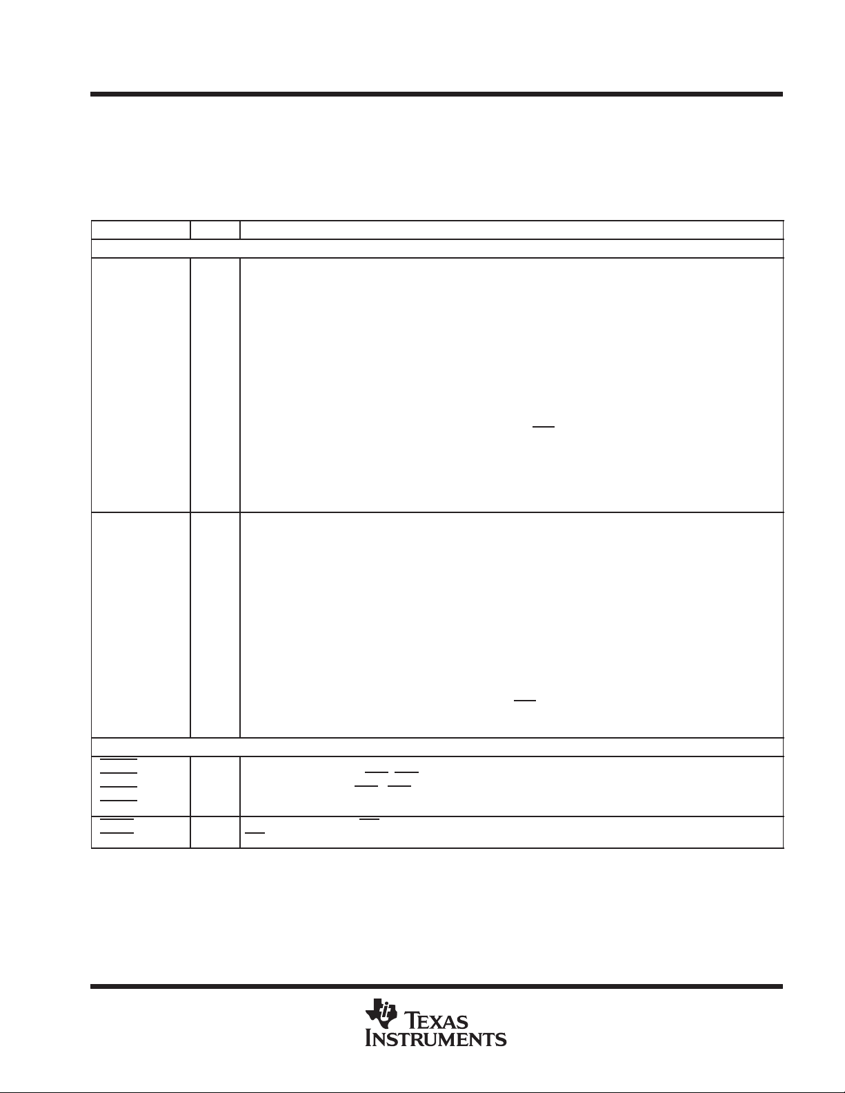
Pin Assignments for the TMS320VC5420PGE
(144-Pin Thin Quad Flatpack) (Continued)
PRIMARY
SIGNAL NAME
PPA10 73 PPA11 74
DV
DD
PPA12 77 PPA13 78
HPIRS 79 HMODE 80
B_CLKOUT 81 B_XF 82
B_RS 83 XIO 84
TEST 85 V
CV
DD
B_BDX1 89 V
B_BFSX1 91 B_BCLKR1 92
V
SS
B_BDR1 95 B_BFSR1 96
B_GPIO0 97 B_GPIO1 98
B_GPIO2/BIO 99
B_NMI 101 B_INT1 102
B_INT0 103 PPA17 104
PPA16 105 V
PPA15 107 PPA14 108
PPA7 109 PPA6 110
PPA4 HAS 111 DV
PPA5 113 PPA1 B_HINT 114
PPD3 HD3 115 PPD2 HD2 116
B_BFSR2 117 B_BDR2 118
V
SS
B_BCLKR2 121 B_BFSX2 122
B_BDX2 123 B_BCLKX2 124
V
SS
V
SSA
CLKIN 129 DV
READY HRDY 131 A_BCLKX2 132
CV
DD
A_BCLKR2 135 A_BDR2 136
A_BFSR2 137 A_BDX2 138
A_BFSX2 139 PPD6 HD6 140
PPD4 HD4 141 PPD5 HD5 142
PPD0 HD0 143 V
SECONDARY
SIGNAL NAME
PIN
NO.
75 V
87 B_BCLKX1 88
93 CV
119 CV
125 AV
127 NC 128
133 V
PRIMARY
SIGNAL NAME
SS
SS
SS
DD
IS
SS
DD
DD
DD
DD
SS
SS
SECONDARY
SIGNAL NAME
B_GPIO3
PIN
NO.
76
86
90
94
100
106
112
120
126
130
134
144
6
POST OFFICE BOX 1443 • HOUSTON, TEXAS 77251–1443
Page 7
TMS320VC5420
PRIMARY
SECONDARY
BALL
PRIMARY
SECONDARY
BALL
FIXED-POINT DIGITAL SIGNAL PROCESSOR
SPRS080C – MARCH 1999 – REVISED APRIL 2000
Pin Assignments for the TMS320VC5420GGU
(144-Pin MicroStar Ball Grid Array)
PRIMARY SECONDARY BALL PRIMARY SECONDARY BALL
SIGNAL NAME
PPD7 HD7 A1 PPA8 B1
DV
DD
A_RS E1 CV
A_BDR1 G1 CV
A_XF J1 TMS K1
EMU1/OFF L1 EMU0 M1
V
SS
V
SS
A_INT1 D2 A_GPIO1 E2
V
SS
V
SS
TDI K2 DV
TDO M2 PPD15 HD15 N2
PDD6 HD6 A3 PPD4 HD4 B3
PPD5 HD5 C3 PPD1 HD1 D3
A_GPIO2/BIO E3 V
A_BCLKR1 G3 A_BDX1 H3
VCO J3 TRST K3
A_INT0 L3 PPD14 HD14 M3
V
SS
A_BDX2 B4 A_BFSX2 C4
PPA9 D4 IOSTRB
A_GPIO0 F4 A_BFSX1 G4
A_BCLKX1 H4 TCK J4
PPD13 HD13 K4 PPD12 HD12 L4
A_BFSR0 M4 A_BDR0 N4
CV
DD
A_BCLKR2 C5 A_BDR2 D5
A_BCLKR0 K5 A_BFSX0 L5
V
SS
CLKIN A6 DV
READY HRDY C6 A_BCLKX2 D6
A_BDX0 K6 A_BCLKX0 L6
MSTRB HCS M6 DS HDS2 N6
AV
DD
V
SSA
DV
DD
SIGNAL NAME
NO.
C1 A_NMI D1
N1 PPD0 HD0 A2
B2 PPA0 A_HINT C2
F2 A_BFSR1 G2
H2 A_CLKOUT J2
N3 A_BFSR2 A4
A5 V
M5 CV
A7 V
C7 NC D7
K7 B_BDX0 L7
SIGNAL NAME
DD
DD
DD
SS
SS
DD
DD
SS
SIGNAL NAME
A_GPIO3
A_TOUT
NO.
F1
H1
L2
F3
E4
B5
N5
B6
B7
POST OFFICE BOX 1443 • HOUSTON, TEXAS 77251–1443
7
Page 8
TMS320VC5420
FIXED-POINT DIGITAL SIGNAL PROCESSOR
SPRS080C – MARCH 1999 – REVISED APRIL 2000
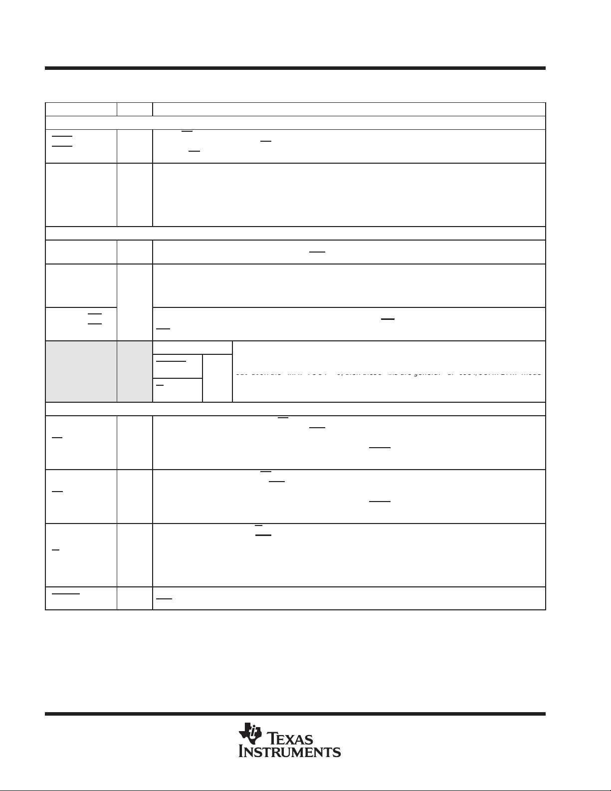
Pin Assignments for the TMS320VC5420GGU
(144-Pin MicroStar Ball Grid Array) (Continued)
PRIMARY
PRIMARY
SIGNAL NAME
SIGNAL NAME
PS HDS1 M7 B_BCLKX0 N7
B_BCLKX2 A8 B_BDX2 B8
B_BFSX2 C8 B_BCLKR2 D8
B_BDR0 K8 B_BCLKR0 L8
B_BFSX0 M8 V
CV
DD
B_BDR2 C9 B_BFSR2 D9
R/W HR/W K9 B_BFSR0 L9
V
SS
PPD2 HD2 A10 PPD3 HD3 B10
PPA1 B_HINT C10 PPA5 D10
IS
B_BCLKR1 G10 TEST H10
B_CLKOUT J10 PPA12 K10
SELA/B L10 PPA3 HCNTL0 M10
PPA2 HCNTL1 N10 DV
PPA4 HAS B11 V
B_INT0 D11 B_GPIO2/BIO E11
B_BDR1 F11 B_BFSX1 G11
V
SS
PPA13 K11 PPD10 HD10 L11
PPD9 HD9 M11 PPD8 HD8 N11
PPA6 A12 PPA14 B12
PPA16 C12 B_INT1 D12
B_GPIO1 E12 CV
B_BDX1 G12 CV
B_RS J12 HPIRS K12
DV
DD
PPD11 HD11 N12 PPA7 A13
PPA15 B13 PPA17 C13
B_NMI D13 B_GPIO0 E13
V
SS
B_BCLKX1 H13 XIO J13
HMODE K13 V
PPA11 M13 PPA10 N13
SECONDARY
SECONDARY
SIGNAL NAME
SIGNAL NAME
B_GPIO3
B_TOUT
BALL
BALL
NO.
NO.
A9 V
M9 CV
E10 B_BFSR1 F10
H11 B_XF J11
L12 V
F13 V
PRIMARY
PRIMARY
SIGNAL NAME
SIGNAL NAME
SS
SS
DD
DD
SS
DD
DD
SS
SS
SS
SECONDARY
SECONDARY
SIGNAL NAME
SIGNAL NAME
BALL
BALL
NO.
NO.
N8
B9
N9
A11
C11
F12
H12
M12
G13
L13
8
POST OFFICE BOX 1443 • HOUSTON, TEXAS 77251–1443
Page 9
TMS320VC5420
5
PPA15
y
PPA12
Parallel ort address bus. The DSP can access the external memory locations by way of the external memory
(
PPA9
The PPA[17:0] ins are also multi lexed with the HPI interface. In HPI mode (XIO in is low), the external address
PPA6
PPA3
FIXED-POINT DIGITAL SIGNAL PROCESSOR
SPRS080C – MARCH 1999 – REVISED APRIL 2000
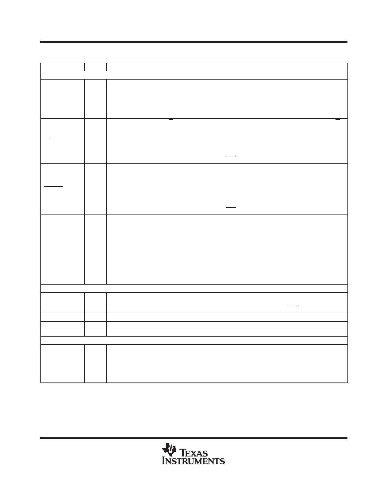
signal descriptions
The ’5420 signal descriptions table lists each pin name, function, and operating mode(s) for the ’5420 device.
Some of the ’5420 pins can be configured for one of two functions; a primary function and a secondary function.
The names of these pins in secondary mode are shaded in grey in the following table.
Signal Descriptions
I/O/Z
I/O/Z
†
DATA SIGNALS
Parallel port address bus. The DSP can access the external memory locations by way of the external memor
interface using PPA[17:0] in external memory interface (EMIF) mode when the XIO pin is logic high.
The PPA[17:0] pins are also multiplexed with the HPI interface. In HPI mode
pins PPA[17:0] are used by a host processor for access to the memory map by way of the on-chip HPI. Refer
to the HPI section of this table for details on the secondary functions of these pins.
These pins are placed into the high-impedance state when OFF is low.
Parallel port data bus. The DSP uses this bidirectional data bus to access external memory when the device is
in external memory interface (EMIF) mode (the XIO pin is logic high).
This data bus is also multiplexed with the 16-bit HPI data bus. When in HPI mode, the bus is used to transfer data
between the host processor and internal DSP memory via the HPI. Refer to the HPI section of this table for details
on the secondary functions of these pins.
¶
The data bus includes bus holders to reduce power dissipation caused by floating, unused pins. The bus holders
also eliminate the need for external pullup resistors on unused pins. When the data bus is not being driven by
the ’5420, the bus holders keep data pins at the last driven logic level. The data bus keepers are disabled at reset
and can be enabled/disabled via the BH bit of the BSCR register.
These pins are placed into high-impedance state when OFF
INITIALIZATION, INTERRUPT, AND RESET OPERATIONS
External user interrupts. INT0–INT3 are prioritized and are maskable by the interrupt mask register (IMR) and
I
the interrupt mode bit. INT0
Nonmaskable interrupt. NMI is an external interrupt that cannot be masked by way of the INTM or the IMR. When
I
NMI
is activated, the processor traps to the appropriate vector location.
–INT3 can be polled and reset by way of the interrupt flag register (IFR).
DESCRIPTION
NAME TYPE
PPA17 (MSB)
PPA16
PPA1
PPA14
PPA13
PPA12
PPA11
PPA10
PPA9
PPA8
PPA7
PPA6
PPA5
‡§
PPA4
PPA3
PPA2
PPA1
PPA0 (LSB)
PPD15 (MSB)
PPD14
PPD13
PPD12
PPD11
PPD10
PPD9
PPD8
PPD7
PPD6
PPD5
PPD4
PPD3
PPD2
PPD1
PPD0 (LSB)
§
A_INT0
§
B_INT0
§
A_INT1
§
B_INT1
§
A_NMI
§
B_NMI
†
I = Input, O = Output, S = Supply, Z = High Impedance
‡
This pin has an internal pullup resistor.
§
These pins have Schmitt trigger inputs.
¶
This pin has an internal bus holder controlled by way of the BSCR register in subchip A.
#
This pin is used by Texas Instruments for device testing and should be left unconnected.
||
This pin has an internal pulldown resistor.
XIO pin is low), the external address
is low.
POST OFFICE BOX 1443 • HOUSTON, TEXAS 77251–1443
9
Page 10
TMS320VC5420
I/O
Wh
HPI
HMODE
ltipl
d
out ut on the in. IF TOUT 0, then these ins are general ur ose I/Os. In EMIF mode
FIXED-POINT DIGITAL SIGNAL PROCESSOR
SPRS080C – MARCH 1999 – REVISED APRIL 2000
Signal Descriptions (Continued)
NAME DESCRIPTIONTYPE
§
A_RS
§
B_RS
XIO I
A_XF
B_XF
A_GPIO0
B_GPIO0
A_GPIO1
B_GPIO1
A_GPIO2/BIO
B_GPIO2/BIO
A_GPIO3
(A_TOUT)
B_GPIO3
(B_TOUT)
‡
PS
‡
DS
IS O
‡§
MSTRB
†
I = Input, O = Output, S = Supply, Z = High Impedance
‡
This pin has an internal pullup resistor.
§
These pins have Schmitt trigger inputs.
¶
This pin has an internal bus holder controlled by way of the BSCR register in subchip A.
#
This pin is used by Texas Instruments for device testing and should be left unconnected.
||
This pin has an internal pulldown resistor.
†
INITIALIZATION, INTERRUPT, AND RESET OPERATIONS (CONTINUED)
Reset. RS causes the digital signal processor (DSP) to terminate execution and causes a reinitialization of the
CPU and peripherals. When RS
I
memory. RS
The XIO pin is used to configure the parallel port as a host-port interface (HPI mode when XIO pin is low), or as
an asynchronous memory interface (EMIF mode when XIO pin is high).
At device reset, the logic combination of the XIO, HMODE, and SELA/B pin levels determines the initialization
value of the MP/MC bit (a bit in the processor mode status (PMST) register ) Refer to the memory section for
details.
External flag output (latched software-programmable output-only signal). Bit addressable. A_XF and B_XF are
O
placed into the high-impedance state when OFF
General-purpose I/O pins (software-programmable I/O signal). V alues can be latched (output) by writing into the
GPIO register. The states of GPIO pins (inputs) can be read by reading the GPIO register. The GPIO direction
is also programmable by way of the DIRn field in the GPIO register.
I/O
General-purpose I/O. These pins can be configured in the same manner as GPIO0–1; however in input mode,
the pins also operate as the traditional branch control bit (BIO
-conditional instructions, these pins operate as general inputs.
BIO
IOSTRB
I/O
IS
Program space select signal. The PS signal is asserted during external program space accesses. This pin is
placed into the high-impedance state when OFF
O
This pin is also multiplexed with the HPI, and functions as the HDS1
to the HPI section of this table for details on the secondary function of this pin.
Data space select signal. The DS signal is asserted during external data space accesses. This pin is placed into
the high-impedance state when OFF
O
This pin is also multiplexed with the HPI, and functions as the HDS2
to the HPI section of this table for details on the secondary function of this pin.
I/O space select signal. The IS signal is asserted during external I/O space accesses. This pin is placed into the
high-impedance state when OFF
This pin is also multiplexed with the general purpose I/O feature, and functions as the B_GPIO3 (B_TOUT)
input/output signal in HPI mode. Refer to the General Purpose I/O section of this table for details on the secondary
function of this pin.
Program and data memory strobe (active in EMIF mode). This pin is placed into the high-impedance state when
O
OFF
affects various registers and status bits.
GENERAL-PURPOSE I/O SIGNALS
PRIMARY
by the general-purpose I/O control register. TOUT bit must be set to “1” to drive the timer
output on the pin. IF TOUT = 0, then these pins are general-purpose I/Os. In EMIF mode
O
(XIO pin high), these signals serve their primary functions and are active during external
I/O space accesses.
MEMORY CONTROL SIGNALS
is low.
is brought to a high level, execution begins at location 0FF80h of program
is low.
en the device is in
is low.
is low.
mode and
is low.
). If application code does not perform
= 0 (mu
data strobe input signal in HPI mode. Refer
data strobe input signal in HPI mode. Refer
p
exed), these pins are controlle
p
10
POST OFFICE BOX 1443 • HOUSTON, TEXAS 77251–1443
Page 11
FIXED-POINT DIGITAL SIGNAL PROCESSOR
Signal Descriptions (Continued)
TMS320VC5420
SPRS080C – MARCH 1999 – REVISED APRIL 2000
NAME DESCRIPTIONTYPE
READY I
R/W O
IOSTRB O
SELA/B I
†
MEMORY CONTROL SIGNALS (CONTINUED)
Data-ready input signal. READY indicates that the external device is prepared for a bus transaction to be
completed. If the device is not ready (READY = 0), the processor waits one cycle and checks READY again. The
processor performs the READY detection if at least two software wait states are programmed.
This pin is also multiplexed with the HPI, and functions as the Host-port data ready (output) in HPI mode. Refer
to the HPI section of this table for details on the secondary function of this pin.
Read/write output signal. R/W indicates transfer direction during communication to an external device. R/W is
normally in the read mode (high), unless it is asserted low when the DSP performs a write operation.
This pin is also multiplexed with the HPI, and functions as the Host-port Read/write input in HPI mode. Refer to
the HPI section of this table for details on the secondary function of this pin.
This pin is placed into the high-impedance state when OFF
I/O space memory strobe. External I/O space is accessible by the CPU and not the direct memory access (DMA)
controller. The DMA has its own dedicated I/O space that is not accessible by the CPU.
This pin is also multiplexed with the general pupose I/O feature, and functions as the A_GPIO3(A_TOUT) signal
in HPI mode. Refer to the general purpose I/O section of this table for details on the secondary function of this
pin.
This pin is placed into the high-impedance state when OFF
The SELA/B pin designates which DSP subsystem has access to the parallel-port interface. Furthermore, this
pin determines which subsystem is accessible by the host via the HPI.
For external memory accesses (XIO pin high), when SELA/B is low subsystem A has control of the external
memory interface. Similarly, when SELA/B is high subsystem B has control.
See Table 7 for a truth table of SELA/B, HMODE and XIO pins and functionality.
is low.
is low.
At device reset, the logic combination of the XIO, HMODE, and SELA/B pin levels determines the initialization
value of the MP/MC bit (a bit in the processor mode status (PMST) register ) Refer to the memory section for
details.
CLOCKING SIGNALS
A_CLKOUT
B_CLKOUT
§
CLKIN
VCO O
A_BCLKR0
B_BCLKR0
A_BCLKR1
B_BCLKR1
A_BCLKR2
B_BCLKR2
†
I = Input, O = Output, S = Supply, Z = High Impedance
‡
This pin has an internal pullup resistor.
§
These pins have Schmitt trigger inputs.
¶
This pin has an internal bus holder controlled by way of the BSCR register in subchip A.
#
This pin is used by Texas Instruments for device testing and should be left unconnected.
||
This pin has an internal pulldown resistor.
‡§
‡§
‡§
‡§
‡§
‡§
I/O/Z
Master clock output signal. CLKOUT cycles at the machine-cycle rate of the CPU. The internal machine cycle
is bounded by the falling edges of this signal. The CLKOUT pin can be turned off by writing a “1” to the CLKOFF
O
bit of the PMST register. CLKOUT goes into the high-impedance state when EMU1/OFF
I Input clock to the device. CLKIN connects to an oscillator circuit/device.
VCO is the output of the voltage-controlled oscillator stage of the PLL. This is a 3-state output during normal
operation. Active in silicon test/debug mode.
MULTICHANNEL BUFFERED SERIAL PORT 0, 1, AND 2 SIGNALS
Receive clocks. BCLKR serves as the serial shift clock for the buffered serial-port receiver . Input from an external
clock source for clocking data into the McBSP. When not being used as a clock, these pins can be used as
general-purpose I/O by setting RIOEN = 1.
BCLKR can be configured as an output by the way of the CLKRM bit in the PCR register.
is low.
POST OFFICE BOX 1443 • HOUSTON, TEXAS 77251–1443
11
Page 12
TMS320VC5420
(
mode (HMODE in is high), to address the on-chi RAM of the 5420. These ins are
FIXED-POINT DIGITAL SIGNAL PROCESSOR
SPRS080C – MARCH 1999 – REVISED APRIL 2000
Signal Descriptions (Continued)
NAME DESCRIPTIONTYPE
A_BCLKX0
B_BCLKX0
A_BCLKX1
B_BCLKX1
A_BCLKX2
B_BCLKX2
A_BDR0
B_BDR0
A_BDR1
B_BDR1
A_BDR2
B_BDR2
A_BDX0
B_BDX0
A_BDX1
B_BDX1
A_BDX2
B_BDX2
A_BFSR0
B_BFSR0
A_BFSR1
B_BFSR1
A_BFSR2
B_BFSR2
A_BFSX0
B_BFSX0
A_BFSX1
B_BFSX1
A_BFSX2
B_BFSX2
HA[0:17] I PPA[0:17] O
HD[0:15] I/O/Z PPD[0:15]
†
I = Input, O = Output, S = Supply, Z = High Impedance
‡
This pin has an internal pullup resistor.
§
These pins have Schmitt trigger inputs.
¶
This pin has an internal bus holder controlled by way of the BSCR register in subchip A.
#
This pin is used by Texas Instruments for device testing and should be left unconnected.
||
This pin has an internal pulldown resistor.
‡§
‡§
‡§
‡§
‡§
‡§
†
MULTICHANNEL BUFFERED SERIAL PORT 0, 1, AND 2 SIGNALS (CONTINUED)
Transmit clocks. Clock signal used to clock data from the transmit register. This pin can also be configured as
an input by setting the CLKXM = 0 in the PCR register. BCLKX can be sampled as an input by way of the IN1
I/O/Z
I/O/Z
I/O/Z
bit in the SPC register. When not being used as a clock, these pins can be used as general-purpose I/O by setting
XIOEN = 1.
These pins are placed into the high-impedance state when OFF
Buffered serial data receive (input) pin. When not being used as data-receive pins, these pins can be used as
I
general-purpose I/O by setting RIOEN = 1.
Buffered serial-port transmit (output) pin. When not being used as data-transmit pins, these pins can be used as
general-purpose I/O by setting XIOEN = 1. These pins are placed into the high-impedance state when OFF
O/Z
low.
Frame synchronization pin for buffered serial-port input data. The BFSR pulse initiates the receive-data process
over BDR pin.
general-purpose I/O by setting RIOEN = 1.
Buffered serial-port frame synchronization pin for transmitting data. The BFSX pulse initiates the transmit-data
process over BDX pin. If RS
by the reset operation.
general-purpose I/O by setting XIOEN = 1. These pins are placed into the high-impedance state when OFF
low.
PRIMARY
When not being used as data-receive synchronization pins, these pins can be used as
is asserted when BFSX is configured as output, then BFSX is turned into input mode
When not being used as data-transmit synchronization pins, these pins can be used as
HOST-PORT INTERFACE SIGNALS
HPI address inputs. HA[0:17] are used by the host device, in the HPI non-multiplexed
HMODE pin is high), to address the on-chip RAM of the ’5420. These pins are
mode
shared with the external memory interface and are only used by the HPI when the interface
is in HPI mode (XIO pin is low).
Parallel bidirectional data bus. HD[0:15] are used by the host device to transfer data to
and from the on-chip RAM of the ’5420. These pins are shared with the external memory
interface and are only used by the HPI when the interface is in HPI mode (XIO pin is low).
The data bus includes bus holders to reduce power dissipation caused by floating, unused
I/O/Z
pins. The bus holders also eliminate the need for external pullup resistors on unused pins.
When the data bus is not being driven by the ’5420, the bus holders keep data pins at the
last driven logic level. The data bus keepers are disabled at reset and can be
enabled/disabled via the BH bit of the BSCR register. These pins are placed into the
high-impedance state when OFF
is low.
is
is
is low.
12
POST OFFICE BOX 1443 • HOUSTON, TEXAS 77251–1443
Page 13
FIXED-POINT DIGITAL SIGNAL PROCESSOR
Signal Descriptions (Continued)
TMS320VC5420
SPRS080C – MARCH 1999 – REVISED APRIL 2000
NAME DESCRIPTIONTYPE
HCNTL0
HCNTL1
‡§
HAS
‡§
HCS
‡§
HDS1
‡§
HDS2
HR/W I R/W O
HRDY O READY I
A_HINT
B_HINT
§
HPIRS
HMODE I
AV
DD
CV
DD
DV
DD
V
SS
†
I = Input, O = Output, S = Supply, Z = High Impedance
‡
This pin has an internal pullup resistor.
§
These pins have Schmitt trigger inputs.
¶
This pin has an internal bus holder controlled by way of the BSCR register in subchip A.
#
This pin is used by Texas Instruments for device testing and should be left unconnected.
||
This pin has an internal pulldown resistor.
†
HOST-PORT INTERFACE SIGNALS (CONTINUED)
PRIMARY
HPI control inputs. The HCNTL0 and HCNTL1 values between HPIA, and HPID registers
PPA3
I
PPA2
I PPA4
I MSTRB
I
O
I Host-port interface (HPI) reset pin. This signal resets the host port interface and both subsystems.
S Dedicated power supply that powers the PLL. AVDD = 1.8 V. AVDD can be connected to CVDD.
S Dedicated power supply that powers the core CPUs. CVDD = 1.8 V
S Dedicated power supply that powers the I/O pins. DVDD = 3.3 V
S Digital ground. Dedicated ground plane for the device.
‡§
‡§
‡§
PS
‡§
DS
PPA0
PPA1
Host mode select. When this pin is low it selects the HPI multiplexed address/data mode. The multiplexed
address/data mode allows hosts with multiplexed address/data lines access to the HPI registers HPIC, HPIA,
and HPID. Host-to-DSP and DSP-to-host interrupts are supported in this mode.
When HMODE is high, it selects the HPI nonmultiplexed mode. HPI nonmultiplexed mode allows hosts with
separate address/data buses to access the HPI address range by way of the 18-bit address bus and the HPI data
(HPID) register via the 16-bit data bus. Host-to-DSP and DSP-to-host interrupts are not supported in this mode.
during HPI reads and writes. These signals are only used in HPI multiplexed address/data
mode (HMODE pin is low).
O
These pins are shared with the external memory interface and are only used by the HPI
when the interface is in HPI mode (XIO pin is low).
Address strobe input. Hosts with multiplexed address and data pins require HAS to latch
the address in the HPIA register. This signal is only used in HPI multiplexed address/data
mode (HMODE pin is low).
O
This pin is shared with the external memory interface and is only used by the HPI when
the interface is in HPI mode (XIO pin is low).
HPI chip-select signal. Thissignal must be active during HPI transfers, and can remain
active between concurrent transfers.
O
This pin is shared with the external memory interface and is only used by the HPI when
the interface is in HPI mode (XIO pin is low).
HPI data strobes. HDS1 and HDS2 are driven by the host read and write strobes to control
transfer HPI transfers.
O
These pins are shared with the external memory interface and are only used by the HPI
when the interface is in HPI mode (XIO pin is low).
HPI read/write signal. This signal is used by the host to control the direction of an HPI
transfer.
This pin is shared with the external memory interface and is only used by the HPI when
the interface is in HPI mode (XIO pin is low).
HPI data-ready output. The ready output informs the host when the HPI is ready for the
next transfer.
This pin is shared with the external memory interface and is only used by the HPI when
the interface is in HPI mode (XIO pin is low). HRDY is placed into the high-impedance state
when OFF
Host interrupt pin. HPI can interrupt the host by asserting this low. The host can clear this
interrupt by writing a “1” to the HINT
O
multiplexed address/data mode (HMODE pin is low). These pins are placed into the
high-impedance state when OFF
is low.
SUPPLY PINS
bit of the HPIC register. Only supported in HPI
is low.
POST OFFICE BOX 1443 • HOUSTON, TEXAS 77251–1443
13
Page 14
TMS320VC5420
FIXED-POINT DIGITAL SIGNAL PROCESSOR
SPRS080C – MARCH 1999 – REVISED APRIL 2000
Signal Descriptions (Continued)
NAME DESCRIPTIONTYPE
V
SSA
#
TEST
‡§
TCK
‡
TDI
TDO O
‡
TMS
||
TRST
EMU0 I/O/Z
EMU1/OFF I/O/Z
†
SUPPLY PINS (CONTINUED)
Analog ground. Dedicated ground for the PLL. V
S
not separated.
TEST PIN
No connection
EMULATION/TEST PINS
Standard test clock. This is normally a free-running clock signal with a 50% duty cycle. Changes on the test
access port (TAP) of input signals TMS and TDI are clocked into the TAP controller, instruction register, or
I
selected test-data register on the rising edge of TCK. Changes at the TAP output signal (TDO) occur on the falling
edge of TCK.
Test data input. Pin with an internal pullup device. TDI is clocked into the selected register (instruction or data)
I
on a rising edge of TCK.
Test data pin. The contents of the selected register is shifted out of TDO on the falling edge of TCK. TDO is in
high-impedance state except when the scanning of data is in progress. These pins are placed into high-impedance state when OFF
Test mode select. Pin with internal pullup device. This serial control input is clocked into the TAP controller on
I
the rising edge of TCK.
T est reset. When high, TRST gives the scan system control of the operations of the device. If TRST is driven low,
the device operates in its functional mode and the emulation signals are ignored. Pin with internal pulldown
I
device.
Emulator interrupt 0 pin. When TRST is driven low, EMU0 must be high for the activation of the EMU1/OFF
condition. When TRST is driven high, EMU0 is used as an interrupt to or from the emulator system and is defined
as I/O.
Emulator interrupt 1 pin. When TRST is driven high, EMU1/OFF is used as an interrupt to or from the emulator
system and is defined as I/O. When TRST
= 0 puts all output drivers into the high-impedance state.
Note that OFF is used exclusively for testing and emulation purposes (and not for multiprocessing applications).
Therefore, for the OFF
is low.
transitions from high to low, then EMU1 operates as OFF. EMU/OFF
condition, the following conditions apply:
can be connected to VSS if digital and analog grounds are
SSA
TRST = 0, EMU0 = 1, EMU1 = 0
†
I = Input, O = Output, S = Supply, Z = High Impedance
‡
This pin has an internal pullup resistor.
§
These pins have Schmitt trigger inputs.
¶
This pin has an internal bus holder controlled by way of the BSCR register in subchip A.
#
This pin is used by Texas Instruments for device testing and should be left unconnected.
||
This pin has an internal pulldown resistor.
14
POST OFFICE BOX 1443 • HOUSTON, TEXAS 77251–1443
Page 15
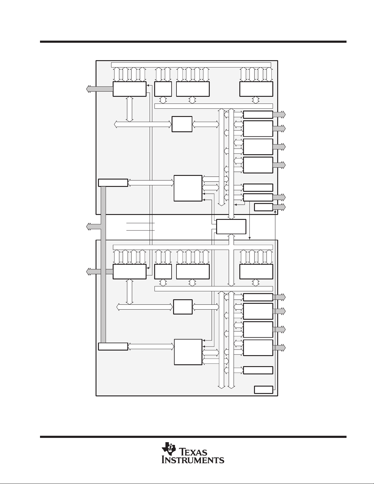
functional overview
TMS320VC5420
FIXED-POINT DIGITAL SIGNAL PROCESSOR
SPRS080C – MARCH 1999 – REVISED APRIL 2000
P, C, D, E Buses and Control Signals
Pbus
’C54x Core A
Modified HPI16
DSP Subsystem A
Interprocessor IRQ’s
Cbus
Dbus
CPU BUS
Host Access Bus
Ebus
Cbus
Pbus
Ebus
36K
Program
SARAM
Peripheral
Bus
Bridge
(6 channels)
P, C, D, E Buses and Control Signals
Dbus
Pbus
48K Prog/Data
SARAM
Peripheral Bus
DMA
Ebus
DMA Bus
Pheripheral Bus
DMA BusDMA Bus
Clocks
Core-to-Core
FIFO Interface
Cbus
Dbus
Pbus
16K Prog/Data
DARAM
GPIO[3:0]
McBSP0
McBSP1
McBSP2
TIMER
APLL
JTAG
Ebus
Pbus
’C54x Core B
Modified HPI16
DSP Subsystem B
Ebus
Cbus
Dbus
Host Access Bus
CPU Bus
Pbus
36K
Program
SARAM
Ebus
Peripheral
Bridge
Pbus
Cbus
48K Prog/Data
SARAM
Bus
Peripheral Bus
DMA
(6 channels)
Dbus
Ebus
DMA Bus
Figure 1. Functional Block Diagram
DMA Bus
Peripheral Bus
Pbus
Cbus
Dbus
16K Prog/Data
DARAM
GPIO[3:0]
McBSP0
McBSP1
McBSP2
TIMER
JTAG
Ebus
POST OFFICE BOX 1443 • HOUSTON, TEXAS 77251–1443
15
Page 16

TMS320VC5420
FIXED-POINT DIGITAL SIGNAL PROCESSOR
SPRS080C – MARCH 1999 – REVISED APRIL 2000
memory
The total memory address range for each ’5420 subsystem is 384K 16-bit words. The memory space is divided
into three specific memory segments: 256K-word program, 64K-word data, and 64K-word I/O. The program
memory space contains the instructions to be executed as well as tables used in execution. The data memory
space stores data used by the instructions. The I/O memory space is used to interface to external
memory-mapped peripherals and can also serve as extra data storage space. The CPU I/O space should not
be confused with the DMA I/O space, which is completely independent and not accessible by the CPU.
on-chip dual-access RAM (DARAM)
The ’5420 subsystems A and B each have 16K
Each of these RAM blocks can be accessed twice per machine cycle. This memory is intended primarily to store
data values; however, it can be used to store program as well. At reset, the DARAM is mapped into data memory
space. DARAM can be mapped into program/data memory space by setting the OVL Y bit in the PMST register.
on-chip single-access RAM (SARAM)
The ’5420 subsystems A and B each have 84K-word × 16-bit on-chip SARAM (ten blocks of 8K words each and
one block of 4K words).
Each of these SARAM blocks is a single-access memory . This memory is intended primarily to store data values;
however, it can be used to store program as well. At reset, the SARAM (4000h–7FFFh) is mapped into data
memory space. This memory range can be mapped into program/data memory space by setting the OVL Y bit
in the PMST register. The SARAM at 8000h–FFFFh is program memory at reset and can be configured as
program/data memory by setting the DROM bit. SARAM spaces18000h–1FFFFh and 2F000h–2FFFFh are
mapped as program memory only.
program memory
The ’5420 device features a paged extended memory scheme in program space to allow access of up to 256K
of program memory relative to each subsystem. This extended program memory (each subsystem) is organized
into four pages (0–3), each 64K in length. A hardware pin is used to select which DSP subsystem (A or B) has
control of the external memory interface. To implement the extended program memory scheme, the ’5420
device includes the following features:
× 16-bit on-chip DARAM (2 blocks of 8K words).
Two additional address lines (for a total of 18)
A pin (SELA/B) for external memory interface arbitration between subsystem A and B
data memory
The data memory space on each ’5420 subsystem contains up to 64K 16-bit word addresses. The device
automatically accesses the on-chip RAM when addressing within its bounds. When an address is generated
outside the RAM bounds, the device automatically generates an external access.
parallel I/O ports
Each subsystem of the ’5420 has a total of 64K I/O ports. These ports can be addressed by PORTR and
PORTW . The IS
external devices through the I/O ports while requiring minimal off-chip address-decoding logic. The SELA/B pin
selects which subsystem has access to the external I/O space.
external memory interface
The ’5420 has a single external memory interface shared between both subsystems. The external memory
interface enables the ’5420 subsystems to connect to external memory devices or other parallel interfaces. The
SELA/B pin is used to determine which subsystem has access to the external memory interface. When the
SELA/B pin is low , subsystem A has access to the external memory interface, and when it is high, subsystem
16
signal indicates the read/write access through an I/O port. The devices can interface easily with
POST OFFICE BOX 1443 • HOUSTON, TEXAS 77251–1443
Page 17
TMS320VC5420
FIXED-POINT DIGITAL SIGNAL PROCESSOR
SPRS080C – MARCH 1999 – REVISED APRIL 2000
external memory interface (continued)
B has access to the interface. The external memory interface is also shared with the host port interface (HPI).
The XIO pin is used to select between the external memory interface and the hostport interface. When the XIO
pin is high, the external memory interface is active, and when it is low, the host port interface is active.
processor mode status register (PMST)
Each subsystem has a processor-mode status register (PMST) that controls memory configuration. The bit
layout of the PMST register is shown in Figure 1
15 76543210
IPTR
R/W R/W R/W R/W R/W R/W R/W R/W
LEGEND: R = Read, W = Write
Figure 1. Processor Mode Status Register (PMST) Bit Layout
The functions of the PMST register bits are illustrated in the memory map. The MP/MC bit is used to map the
upper address range of all program space pages (x8000–xFFFF) as either external or internal memory. The
OVL Y bit is used to overlay the on-chip DARAM0 and SARAM1 blocks from dataspace onto to program space.
Similarly, the DROM bit is used to overlay the SARAM2 block from program space onto data space. See the
TMS320C54x DSP CPU and Peripherals Reference Set, Volume 1
description of the other bits of the PMST register.
MP/MC OVLY AVIS DROM CLKOFF SMUL SST
(literature number SPRU131) for a
Due to the dual-processor configuration and the several EMIF/HPI options available, the MP/MC bit is initialized
at the time of device reset to a logic level that is dependent on the XIO, HMODE, and SELA/B pins. Table 1
shows the initialized logic level of the MP/MC bit and how it depends on these pins.
Table 1. MP/MC Bit Logic Levels at Reset
’5420 PINS MP/MC BIT
XIO HMODE SELA/B SUBSYSTEM A SUBSYSTEM B
0 X X 0 0
1 0 X 1 1
1 1 0 1 0
1 1 1 0 1
POST OFFICE BOX 1443 • HOUSTON, TEXAS 77251–1443
17
Page 18

TMS320VC5420
FIXED-POINT DIGITAL SIGNAL PROCESSOR
SPRS080C – MARCH 1999 – REVISED APRIL 2000
memory map
DataHex Program Page 0Hex
0000
005F
0060
007F
0080
3FFF
4000
7FFF
8000
FFFF
†
The external memory interface must be enabled by driving the XIO pin high, in order for external memory accesses to occur.
Memory-
Mapped
Registers
Scratch-Pad
DARAM
On-Chip
DARAM 0
(16K Words)
On-Chip
SARAM 1
(16K Words)
On-Chip
SARAM 2
(32K Words)
Prog/Data
(DROM=1)
External
(DROM=0)
0000
On-Chip
DARAM 0
(16K Words)
Prog/Data
(OVLY=1)
External
†
(OVLY=0)
3FFF
4000
On-Chip
SARAM 1
(16K Words)
Prog/Data
(OVLY=1)
External
†
(OVLY=0)
7FFF
8000
On-Chip
SARAM 2
(32K Words)
Prog/Data
(MP/MC=0)
External
†
(MP/MC=1)
FFFF
†
(extended)
10000
13FFF
14000
17FFF
18000
1FFFF
Program Page 1Hex
On-Chip
DARAM 0
(16K Words)
Prog/Data
(OVLY=1)
External
†
(OVLY=0)
On-Chip
SARAM 1
(16K Words)
Prog/Data
(OVLY=1)
External
†
(OVLY=0)
On-Chip
SARAM 3
(32KWords)
(MP/MC=0)
External
(MP/MC=1)
†
(extended) (extended)
20000
23FFF
24000
27FFF
28000
2EFFF
2F000
2FFFF
Program Page 2Hex
On-Chip
DARAM 0
(16K Words)
Prog/Data
(OVLY=1)
External
(OVLY=0)
On-Chip
SARAM 1
(16K Words)
Prog/Data
(OVLY=1)
External
(OVLY=0)
Reserved
(MP/MC=0)
External
(MP/MC=1)
On-Chip
SARAM 4
(4K Words)
(MP/MC=0)
External
(MP/MC=1)
Program Page 3Hex
30000
On-Chip
DARAM 0
(16K Words)
Prog/Data
(OVLY=1)
†
33FFF
34000
†
37FFF
38000
†
†
3FFFF
External
(OVLY=0)
On-Chip
SARAM 1
(16K Words)
Prog/Data
(OVLY=1)
External
(OVLY=0)
Reserved
(MP/MC=0)
External
(MP/MC=1)
(extended)
†
†
†
0000
FFFF
I/OHex
64K
External
I/O Ports
†
Figure 2. Memory Map for Each CPU Subsystem
multicore reset signals
The ’5420 device includes three reset signals: A_RS, B_RS, and HPIRS. The A_RS and B_RS pins function
as the CPU reset signal for subsystem A and subsystem B, respectively. These signals reset the state of the
CPU registers and upon release, initiates the reset function. Additionally, the A_RS signal resets the on-chip
PLL and initializes the CLKMD register to bypass mode.
The HPI reset signal (HPIRS) places the HPI peripheral into a reset state. It is necessary to wait three clock
cycles after the rising edge of HPIRS
reset vector initialization
The ’5420 device does not have on-chip ROM and therefore does not contain bootloader routines/software.
Consequently , the user must have a valid reset vector in place before releasing the reset signal. This is referred
reset vector initialization
to as
program memory and begins to execute the instructions found in memory . The application code is raw program
and data words and does not require the traditional
before performing an HPI access.
. After reset, the ’5420 device fetches the reset vector at address 0xFF80 in
boot-table
or
boot-packet
format.
18
POST OFFICE BOX 1443 • HOUSTON, TEXAS 77251–1443
Page 19

TMS320VC5420
FIXED-POINT DIGITAL SIGNAL PROCESSOR
SPRS080C – MARCH 1999 – REVISED APRIL 2000
reset vectorinitialization (continued)
The selection of the reset initialization option is determined by the state of three pins; XIO, XMODE, and SELA/B.
The options include:
HPI (host-dependent)
EMIF-to-HPI (stand-alone)
Simultaneous EMIF (stand-alone)
Sequential EMIF (stand-alone)
HPI
The HPI method is only valid when the level of the XIO pin is low. The ’5420 acts as a slave to an external master
host. The host device must keep the ’5420 device in reset as it downloads code to the subsystem that is
determined by the logic level of the SELA/B pin. When SELA/B is low, the master downloads code to
subsystem A. By driving SELA/B high, the master host can subsequently download code to subsystem B. The
HMODE pin determines the configuration of the HPI (multiplexed or nonmultiplexed) and is an asynchronous
input. Therefore, HMODE can be changed to the desired configuration while A_RS
the transfer. Once the subsystem(s) have been loaded and are ready to execute, the master host can release
the reset pin(s).
There are two valid options for controlling the reset function of the subsystems. The first option is to hold the
A_RS and B_RS pins low while the HPIRS pin transitions from low to high. This keeps the cores in reset while
allowing the HPI full access to download the application code. The host can now drive the A_RS
signals high simultaneously or separately to release the respective subsystem from reset. The subsystems then
fetch their respective reset vector. If the subsystems are released from reset seperately, subsystem A should
be released from reset first, since the A_RS pin resets the on-chip PLL that is common to both subsystems.
and B_RS are low prior to
and B_RS
Another valid option is to keep the A_RS and B_RS pins high while the host transitions the HPIRS pin from low
to high. Special internal logic causes the HPI to be fully operable and the cores remain in reset. As a result, after
the host processor has downloaded the application code via the HPI, it must perform an additional HPI write
(any value) to address 0x2F. This releases the respective subsystem from reset. By changing the value of
SELA/B, the host can write to 0x2F via the HPI to release the other subsystem from reset.
EMIF-to-HPI
In this particular vector initialization method, the host processor controlling the HPI is one of the subsystems.
The master host is subsystem A if SELA/B is low and subsystem B when SELA/B is high. As described in the
signal descriptions table, the address, data, and control signals of the program space are multiplexed with the
HPI signals. In a special mode when XIO is high (EMIF mode) and HMODE is high (HPI nonmultiplexed mode),
these multiplexed signals are connected, making it possible for the master subsystem’s EMIF to initialize the
slave subsystem via the slave’s HPI. The master subsystem then releases the slave from reset either by
transitioning the hardware reset signal (x_RS
HPI. As a result, the slave core fetches the reset vector.
) high, or in software, by writing to memory location 0x2F via the
simultaneous EMIF
The simultaneous EMIF vector initialization option allows both subsystems to access external memory
simultaneously . The subsystems are designed to operate synchronized with one another while accessing the
same locations simultaneously . In this mode, when XIO is high and HMODE is low , one subsystem is given full
control of the EMIF while the other subsystem relies on the synchronization of the two subsystems. Instructions
fetched by one subsystem are ready for both subsystems to execute. After the application code is executed or
transferred to internal memory, write accesses to external memory are prohibited.
This method requires the A_RS and B_RS pins to be tied high while HPIRS transitions from low to high. When
HPIRS transitions high, both subsystems fetches the same reset vector .
POST OFFICE BOX 1443 • HOUSTON, TEXAS 77251–1443
19
Page 20

TMS320VC5420
FIXED-POINT DIGITAL SIGNAL PROCESSOR
SPRS080C – MARCH 1999 – REVISED APRIL 2000
sequential EMIF
The sequential EMIF option allows one master subsystem to run from external memory while controlling the
slave subsystem’s RS signal and the SELA/B pin. At system reset, only the master subsystem is actually reset.
Upon a low-to-high transition of the master’s RS signal, the master subsystem fetches the reset vector and
proceeds to copy external application code to internal memory space. The master subsystem begins executing
the application code, then changes the state of SELA/B, relinquishing the external EMIF to the slave subsystem.
The master then releases the slave RS
the external application code to internal memory space. Note, GPIO pins on the master subsystem can be used
to control the SELA/B and slave reset (x_RS) pins externally.
on-chip peripherals
All the ’54x devices have the same CPU structure; however, they have dif ferent on-chip peripherals connected
to their CPUs. The on-chip peripheral options provided on each subsystem of the ’5420 are:
Software-programmable wait-state generator
Programmable bank-switching
16-bit host-port interface (HPI16)
Multichannel buffered serial ports (McBSPs)
A hardware timer
A software-programmable clock generator with a phase-locked loop (PLL)
signal. As a result, the slave fetches the reset vector and begins to copy
software-programmable wait-state generators
The Software-programmable wait-state generator can be used to extend external bus cycles up to fourteen
machine cycles to interface with slower off-chip memory and I/O devices. Note that all external memory
accesses on the ’5420 require at least one wait state. The software wait-state register (SWWSR) controls the
operation of the wait-state generator. The SWWSR of a particular DSP subsystem (A or B) is used for the
external memory interface, depending on the logic level of the SELA/B pin.The 14 LSBs of the SWWSR specify
the number of wait states (0 to 7) to be inserted for external memory accesses to five separate address ranges.
This allows a different number of wait states for each of the five address ranges.
Additionally, the software wait-state multiplier (SWSM) bit of the software wait-state control register (SWCR)
defines a multiplication factor of 1 or 2 for the number of wait states. At reset, the wait-state generator is initialized
to provide seven wait states on all external memory accesses. The SWWSR bit fields are shown in Figure 3
and described in Table 2.
14 12 11 9 8 6 5 3 2 015
XPA I/O Data Data Program Program
R/W-1 11R/W-0 R/W-111 R/W-111 R/W-1 11 R/W-111
LEGEND: R=Read, W=Write, 0=V alue after reset
Figure 3. Software Wait-State Register (SWWSR) [Memory-Mapped Register (MMR) Address 0028h]
20
POST OFFICE BOX 1443 • HOUSTON, TEXAS 77251–1443
Page 21
FIXED-POINT DIGITAL SIGNAL PROCESSOR
RESET
RESET
software-programmable wait-state generator (continued)
Table 2. Software Wait-State Register (SWWSR) Bit Fields
TMS320VC5420
SPRS080C – MARCH 1999 – REVISED APRIL 2000
BIT
NO. NAME
15 XPA 0
14–12 I/O 1
11–9 Data 1
8–6 Data 1
5–3 Program 1
2–0 Program 1
RESET
VALUE
FUNCTION
Extended program address control bit. XP A is used in conjunction with the program space fields
(bits 0 through 5) to select the address range for program space wait states.
I/O space. The field value (0–7) corresponds to the base number of wait states for I/O space accesses
within addresses 0000–FFFFh. The SWSM bit of the SWCR defines a multiplication factor of 1 or 2 for
the base number of wait states.
Upper data space. The field value (0–7) corresponds to the base number of wait states for external
data space accesses within addresses 8000–FFFFh. The SWSM bit of the SWCR defines a
multiplication factor of 1 or 2 for the base number of wait states.
Lower data space. The field value (0–7) corresponds to the base number of wait states for external
data space accesses within addresses 0000–7FFFh. The SWSM bit of the SWCR defines a
multiplication factor of 1 or 2 for the base number of wait states.
Upper program space. The field value (0–7) corresponds to the base number of wait states for external
program space accesses within the following addresses:
XPA = 0: x8000 – xFFFFh
XPA = 1: The upper program space bit field has no effect on wait states.
The SWSM bit of the SWCR defines a multiplication factor of 1 or 2 for the base number of wait
states.
Program space. The field value (0–7) corresponds to the base number of wait states for external
program space accesses within the following addresses:
XPA = 0: x0000–x7FFFh
XPA = 1: 00000–3FFFFh
The SWSM bit of the SWCR defines a multiplication factor of 1 or 2 for the base number of wait
states.
The software wait-state multiplier bit of the software wait-state control register (SWCR) is used to extend the
base number of wait states selected by the SWWSR. The SWCR bit fields are shown in Figure 4 and described
in Table 3.
115
Reserved
R/W-0
LEGEND: R = Read, W = Write
0
SWSM
R/W-0
Figure 4. Software Wait-State Control Register (SWCR) [MMR Address 002Bh]
Table 3. Software Wait-State Control Register (SWCR) Bit Fields
PIN
NO. NAME
15–1 Reserved 0
0 SWSM 0
RESET
VALUE
FUNCTION
These bits are reserved and are unaffected by writes.
Software wait-state multiplier . Used to multiply the number of wait states defined in the SWWSR by a factor
of 1 or 2.
SWSM = 0: wait-state base values are unchanged (multiplied by 1).
SWSM = 1: wait-state base values are mulitplied by 2 for a maximum of 14 wait states.
POST OFFICE BOX 1443 • HOUSTON, TEXAS 77251–1443
21
Page 22
TMS320VC5420
FIXED-POINT DIGITAL SIGNAL PROCESSOR
SPRS080C – MARCH 1999 – REVISED APRIL 2000
programmable bank-switching
Programmable bank-switching can be used to insert one cycle automatically when crossing memory-bank
boundaries inside program memory or data memory space. One cycle can also be inserted when crossing from
program-memory space to data-memory space (’54x) or one program memory page to another program
memory page. This extra cycle allows memory devices to release the bus before other devices start driving the
bus; thereby avoiding bus contention. The size of the memory bank for the bank-switching is defined by the
bank-switching control register (BSCR). The BSCR of a particular DSP subsystem (A or B) is used for the
external memory interface depending on the logic level of the SELA/B pin.
15 12 11 10 9 8 7 3 2 1 0
BNKCMP
R/W R/W R/W R/W R/W R/W
LEGEND: R = Read, W = Write
PS-DS Reserved IPIRQ Reserved BH Reserved EXIO
Figure 5. BSCR Register Bit Layout for Each DSP Subsystem
Table 4. BSCR Register Bit Functions for Each DSP Subsystem
BIT
NO.
15–12 BNKCMP 1111
11 PS-DS 1
10–9 Reserved 0 These bits are reserved and are unaffected by writes.
8 IPIRQ 0
7–3 Reserved 0 These bits are reserved and are unaffected by writes.
2 BH 0
1 Reserved 0 These bits are reserved and are unaffected by writes.
0 EXIO 0
BIT
NAME
RESET
VALUE
FUNCTION
Bank compare. BNKCMP determines the external memory-bank size. BNKCMP is used to mask the four
MSBs of an address. For example, if BNKCMP = 1111b, the four MSBs (bits 12–15) are compared,
resulting in a bank size of 4K words. Bank sizes of 4K words to 64K words are allowed.
Program read – data read access. PS-DS inserts an extra cycle between consecutive accesses of
program read and data read or data read and program read.
PS-DS = 0 No extra cycles are inserted by this feature.
PS-DS = 1 One extra cycle is inserted between consecutive data and program reads.
The IPIRQ bit is used to send an interprocessor interrupt to the other subsystem. IPIRQ=1 sends the
interrupt. IPIRQ must be cleared before subsequent interrupts can be made. Refer to the interrupts section
for more details
Bus holder. BH controls the data bus holder feature: BH is cleared to 0 at reset.
BH = 0 The bus holder is disabled.
BH = 1 The bus holder is enabled. When not driven, the data bus (PPD[15:0]) is held in the
previous logic level.
External bus interface off. The EXIO bit controls the external bus-off function.
EXIO = 0 The external bus interface functions as usual.
EXIO = 1 The address bus, data bus, and control signals become inactive after completing the
current bus cycle. Note that the DROM, MP/MC
HM bit of ST1 cannot be modified when the interface is disabled.
, and OVLY bits in the PMST and the
22
POST OFFICE BOX 1443 • HOUSTON, TEXAS 77251–1443
Page 23

TMS320VC5420
FIXED-POINT DIGITAL SIGNAL PROCESSOR
SPRS080C – MARCH 1999 – REVISED APRIL 2000
16-bit host-port interface (HPI16)
The HPI16 is an enhanced 16-bit version of the ’C54x 8-bit host-port interface (HPI). The HPI16 is designed
to allow a 16-bit host to access the DSP on-chip memory, with the host acting as the master of the interface.
Figure 6 illustrates the available memory accessible by the HPI. It should be noted that neither the CPU nor DMA
I/O spaces can be accessed using the host-port interface.
16-bit bidirectional host-port interface (HPI16)
Hex
0000
001F
0020
005F
0060
3FFF
4000
7FFF
8000
Program Page 0
Reserved
McBSP
DXR/DRR
MMRegs Only
On-Chip
DARAM 0
(Overlayed)
Prog/Data
On-Chip
SARAM 1
(Overlayed)
Prog/Data
On-Chip
SARAM 2
(32K Words)
Prog/Data
Hex
10000
1005F
10060
13FFF
14000
17FFF
18000
Program Page 1
Reserved
On-Chip
DARAM 0
(Overlayed)
Prog/Data
On-Chip
SARAM 1
(Overlayed)
Prog/Data
On-Chip
SARAM 3
(32K Words)
Program
Hex
20000
2005F
20060
23FFF
24000
27FFF
28000
2EFFF
2F000
Program Page 2
Reserved
On-Chip
DARAM 0
(Overlayed)
Prog/Data
On-Chip
SARAM 1
(Overlayed)
Prog/Data
Reserved
On-Chip
SARAM 4
(4K Words)
Program
Hex
30000
3005F
30060
33FFF
34000
37FFF
38000
Program Page 3
Reserved
On-Chip
DARAM 0
(Overlayed)
Prog/Data
On-Chip
SARAM 1
(Overlayed)
Prog/Data
Reserved
FFFF
1FFFF
2FFFF
Figure 6. Memory Map Relative to Host-Port interface
POST OFFICE BOX 1443 • HOUSTON, TEXAS 77251–1443
3FFFF
23
Page 24

TMS320VC5420
FIXED-POINT DIGITAL SIGNAL PROCESSOR
SPRS080C – MARCH 1999 – REVISED APRIL 2000
16-bit bidirectional host-port interface (HPI16) (continued)
Some of the features of the HPI16 include:
16-bit bidirectional data bus
Multiple data strobes and control signals to allow glueless interfacing to a variety of hosts
Multiplexed
18-bit address bus used in nonmultiplexed mode to allow access to all internal memory (including internal
extended address pages)
18-bit address register used in multiplexed mode. Includes address autoincrement feature for faster
accesses to sequential addresses
Interface to on-chip DMA module to allow access to entire internal memory space
HRDY signal to hold off host accesses due to DMA latency
Control register available in
interrupts, extended addressing, and data prefetch capability
The HPI16 acts as a slave to a 16-bit host processor and allows access to the on-chip memory of the DSP . There
are two modes of operation as determined by the HMODE signal:
HPI multiplexed mode
and
nonmultiplexed address/data modes
multiplexed
mode only . Accessible by either host or DSP to provide host/DSP
multiplexed
mode and
nonmultiplexed
mode.
In
multiplexed
products. A host with a multiplexed address/data bus can access the HPI16 data register (HPID), address
register (HPIA), or control register (HPIC) via the HD bidirectional data bus. The host initiates the access with
the strobe signals (HDS1
signals. The DSP can interrupt the host via the HINT signal, and can stall host accesses via the HRDY signal.
host/DSP interrupts
multiplexed
In
HPIC register.
For host-to-DSP interrupts, the host must write a “1” to the DSPINT bit of the HPIC register. This generates an
interrupt to the DSP . This interrupt can also be used to wake the DSP from any of the IDLE 1,2, or 3 states. Note
that the DSPINT bit is always read as “0” by both the host and DSP.
For DSP-to-host interrupts, the DSP must write a “1” to the HINT bit of the HPIC register to interrupt the host
via the HINT
register. Note that writing a “0” to the HINT bit by either host or DSP has no effect.
mode, HPI16 operation is very similar to the standard 8-bit HPI, which is available with other ’C54x
, HDS2, HCS) and controls the type of access with the HCNTL, HR/W, and HAS
mode, the HPI16 offers the capability for the host and DSP to interrupt each other through the
pin. The host acknowledges and clear this interrupt by also writing a “1” to the HINT bit of the HPIC
HPI nonmultiplexed mode
In
nonmultiplexed
via the HD 16-bit bidirectional data bus, and the address register (HPIA) via the 18-bit HA address bus. The host
initiates the access with the strobe signals (HDS1, HDS2, HCS) and controls the direction of the access with
the HR/W signal. The HPI16 can stall host accesses via the HRDY signal. Note that the HPIC register is not
available in
read or write access.
mode, a host with separate address/data buses can access the HPI16 data register (HPID)
nonmultiplexed
mode since there are no HCNTL signals available. All host accesses initiate a DMA
other HPI16 system considerations
operation during IDLE2
The HPI16 can continue to operate during IDLE1 or IDLE2 by using special clock management logic that turns
on relevant clocks to perform a synchronous memory access, and then turns the clocks back off to save power .
The DSP CPU does not wake up from the IDLE mode during this process.
24
POST OFFICE BOX 1443 • HOUSTON, TEXAS 77251–1443
Page 25

downloading code during reset
TMS320VC5420
FIXED-POINT DIGITAL SIGNAL PROCESSOR
SPRS080C – MARCH 1999 – REVISED APRIL 2000
The HPI16 can download code while the DSP is in reset. However, the system provides a pin (HPIRS
provides a way to take the HPI16 module out of reset while leaving the DSP in reset.
emulation considerations
The HPI16 can continue operation even when the DSP CPU is halted due to debugger breakpoints or other
emulation events.
5420 boundary scan implementation
The ’5420 does not implement a fully compliant IEEE1 149.1 boundary scan capability . Observe-only boundary
scan cells are used on all of the device pins that allow the pins to be observed (read) but not controlled (driven)
using boundary scan. Driving nodes to perform board interconnect test must be accomplished using other
boundary scan capable devices on the board. Although this implies some reduction in testability , compared to
full boundary scan, this implementation is still compatible with the boundary scan automatic test pattern
generation (ATPG) tools.
multichannel buffered serial port (McBSP)
The ’5420 device provides high-speed, full-duplex serial ports that allow direct interface to other ’C54x devices,
codecs, and other devices in a system. There are six multichannel buffered serial ports (McBSPs) on chip (three
per subsystem).
The McBSP is based on the standard serial port interface found on the ’54x devices. Like its predecessors, the
McBSP provides:
Full-duplex communication
Double-buffer data registers, which allow a continuous data stream
Independent framing and clocking for receive and transmit
) that
In addition, the McBSP has the following capabilities:
Direct interface to:
– T1/E1 framers
– MVIP switching-compatible and ST-BUS compliant devices
– IOM-2 compliant device
– Serial peripheral interface devices
Multichannel transmit and receive of up to 128 channels
A wide selection of data sizes, including: 8, 12, 16, 20, 24, or 32 bits
µ-law and A-law companding
Programmable polarity for both frame synchronization and data clocks
Programmable internal clock and frame generation
The McBSP consists of a data path and control path. The six pins, BDX, BDR, BFSX, BFSR, BCLKX, and
BCLKR, connect the control and data paths to external devices. The pins can be programmed as
general-purpose I/O pins if they are not used for serial communication.
Like the standard serial port interface on the McBSP, the data is communicated to devices interfacing to the
McBSP by way of the data transmit (BDX) pin for transmit and the data receive (BDR) pin for receive. Control
information in the form of clocking and frame synchronization is communicated by way of BCLKX, BCLKR,
BFSX, and BFSR. The device communicates to the McBSP by way of 16-bit-wide control registers accessible
via the internal peripheral bus. The CPU or DMA reads the received data from the data receive register (DRR)
and writes the data to be transmitted to the data transmit register (DXR). Data written to the DXR is shifted out
POST OFFICE BOX 1443 • HOUSTON, TEXAS 77251–1443
25
Page 26

TMS320VC5420
FIXED-POINT DIGITAL SIGNAL PROCESSOR
SPRS080C – MARCH 1999 – REVISED APRIL 2000
multichannel buffered serial port (McBSP) (continued)
to BDX by way of the transmit shift register (XSR). Similarly, receive data on the BDR pin is shifted into the
receive shift register (RSR) and copied into the receive buffer register (RBR). RBR is then copied to DRR, which
can be read by the CPU or DMA. This allows internal data movement and external data communications
simultaneously. The control block consists of internal clock generation, frame synchronization signal
generation, and their control, and multichannel selection. This control block sends notification of important
events to the CPU and DMA by way of two interrupt signals, XINT and RINT , and two event signals, XEVT and
REVT.
The on-chip companding hardware allows compression and expansion of data in either µ-law or A-law format.
When companding is used, transmitted data is encoded according to specified companding law and received
data is decoded to 2’s complement format.
The sample rate generator provides the McBSP with several means of selecting clocking and framing for both
the receiver and transmitter. Both the receiver and transmitter can select clocking and framing independently.
The McBSP allows the multiple channels to be independently selected for the transmitter and receiver. When
multiple channels are selected, each frame represents a time-division multiplexed (TDM) data stream. In using
time-division multiplexed data streams, the CPU may only need to process a few of them. Thus, to save memory
and bus bandwidth, multichannel selection allows independent enabling of particular channels for transmission
and reception. Up to 32 channels in a bit stream consisting of a maximum of 128 channels can be enabled.
The clock stop mode (CLKSTP) in the McBSP provides compatibility with the SPI protocol. Clock stop mode
works with only single-phase frames and one word per frame. The word sizes supported by the McBSP are
programmable for 8-, 12-, 16-, 20-, 24-, or 32-bit operation. When the McBSP is configured to operate in SPI
mode, both the transmitter and the receiver operate together as a master or as a slave.
direct memory access unit (DMA)
The ’5420 direct memory access (DMA) controller transfers data between points in the memory map without
intervention by the CPU. The DMA allows movements of data to and from internal program/data memory,
internal peripherals, such as the McBSPs and the HPI to occur in the background of the CPU operation. Each
subsystem has its own independent DMA with six programmable channels, allowing six different contexts for
DMA operation. The HPI has a dedicated auxiliary DMA channel. Figure 7 illustrates the memory map
accessible by the DMA.
26
POST OFFICE BOX 1443 • HOUSTON, TEXAS 77251–1443
Page 27
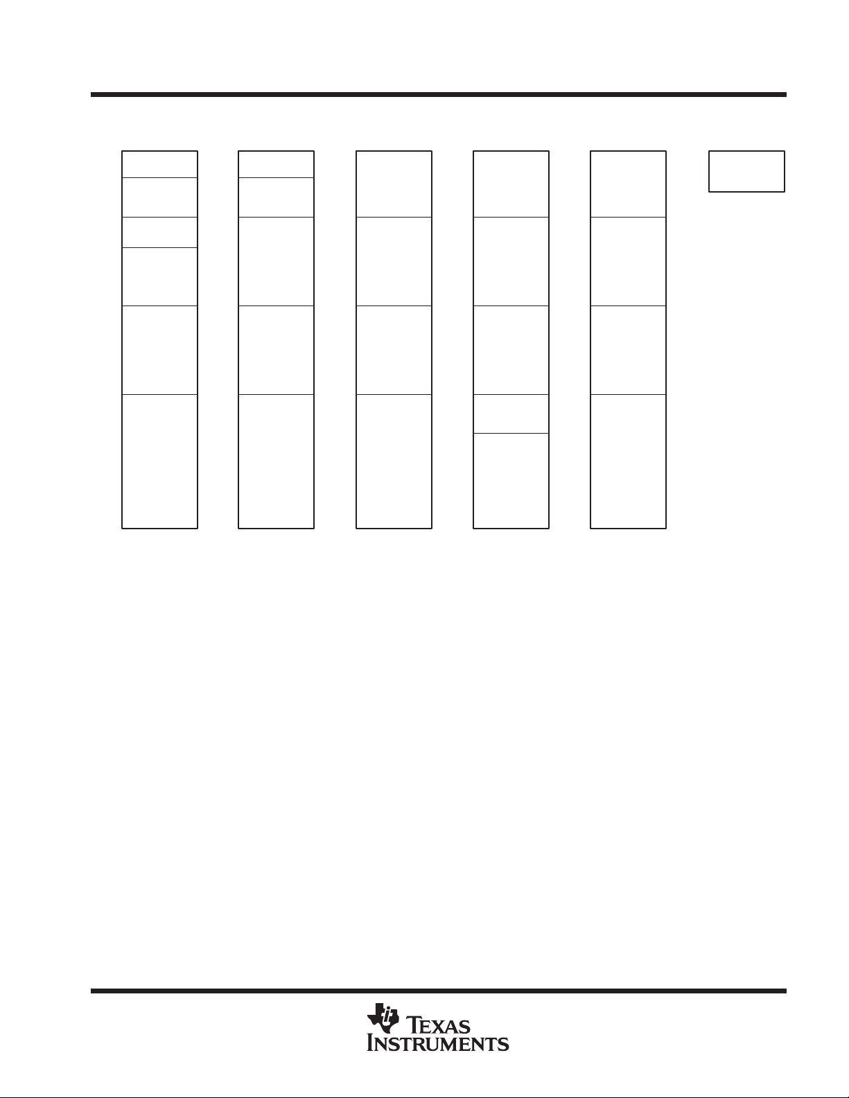
direct memory access unit (DMA) (continued)
TMS320VC5420
FIXED-POINT DIGITAL SIGNAL PROCESSOR
SPRS080C – MARCH 1999 – REVISED APRIL 2000
DataHex Program Page 0Hex
0000
001F
0020
005F
0060
007F
0080
3FFF
4000
7FFF
8000
FFFF
†
When the source or destination for a DMA channel is programmed for I/O space, the channel accesses the core-to-core FIFO irrespective of
Reserved
McBSP
DXR/DRR
MMRegs Only
Scratch-Pad
DARAM
On-Chip
DARAM 0
(16K Words)
On-Chip
SARAM 1
(16K Words)
On-Chip
SARAM 2
(32K Words)
Prog/Data
0000
001F
0020
005F
0060
3FFF
4000
7FFF
8000
FFFF
Reserved
McBSP
DXR/DRR
MMRegs Only
On-Chip
DARAM 0
(Overlayed)
Prog/Data
On-Chip
SARAM 1
(Overlayed)
Prog/Data
On-Chip
SARAM 2
(32K Words)
Prog/Data
10000
1005F
10060
13FFF
14000
17FFF
18000
1FFFF
Program Page 1Hex
Reserved
On-Chip
DARAM 0
(Overlayed)
Prog/Data
On-Chip
SARAM 1
(Overlayed)
Prog/Data
On-Chip
SARAM 3
(32K Words)
Prog/Data
20000
2005F
20060
23FFF
24000
27FFF
28000
2EFFF
2F000
2FFFF
Program Page 2Hex
Reserved
On-Chip
DARAM 0
(Overlayed)
Prog/Data
On-Chip
SARAM 1
(Overlayed)
Prog/Data
Reserved
On-Chip
SARAM 4
(4K Words)
Prog/Data
30000
3005F
30060
33FFF
34000
37FFF
38000
3FFFF
Program Page 3Hex
Reserved
On-Chip
DARAM 0
(Overlayed)
Prog/Data
On-Chip
SARAM 1
(Overlayed)
Prog/Data
Reserved
XXXX
I/OHex
DMA FIFO
for Core-Core
Communication
the address specified.
Figure 7. Memory Map Relative to DMA
features
The ’5420 DMA has the following features:
The DMA operates independently of the CPU.
The DMA has six channels. The DMA can keep track of the contexts of six independent block transfers.
The DMA has higher priority than the CPU for internal accesses.
Each channel has independently programmable priorities.
Each channel’s source and destination address registers can have configurable indexes through memory
on each read and write transfer, respectively. The address can remain constant, postincrement,
postdecrement or be adjusted by a programmable value.
Each read or write transfer can be initialized by selected events.
On completion of a half-block or full-block transfer, each DMA channel can send an interrupt to the CPU.
An on-chip RAM DMA transfer requires 4 clock cycles to complete. External transfers are not supported.
The DMA can perform double word transfers (a 32-bit transfer of two16-bit-words).
POST OFFICE BOX 1443 • HOUSTON, TEXAS 77251–1443
27
Page 28

TMS320VC5420
FIXED-POINT DIGITAL SIGNAL PROCESSOR
SPRS080C – MARCH 1999 – REVISED APRIL 2000
DMA controller synchronization events
The transfers associated with each DMA channel can be synchronized to one of several events. The DSYN bit
field of the DMA channel x sync select and frame count (DMSFCx) register selects the synchronization event
for a channel. The list of possible events and the DSYN values are shown in Table 5.
Table 5. DMA Synchronization Events
DSYN VALUE DMA SYNCHRONIZATION EVENT
0000b No synchronization used
0001b McBSP0 Receive Event
0010b McBSP0 Transmit Event
0011b McBSP2 Receive Event
0100b McBSP2 Transmit Event
0101b McBSP1 Receive Event
0110b McBSP1 Transmit Event
0111b FIFO Receive Buffer Not Empty Event
1000b FIFO Transmit Buffer Not Full Event
1001b – 1111b Reserved
DMA channel interrupt selection
The DMA controller can generate a CPU interrupt for each of the six channels. However, channels 0, 1, 2, and
3 are multiplexed with other interrupt sources. DMA channels 0 and 1 share an interrupt line with the receive
and transmit portions of McBSP2 (IMR/IFR bits 6 and 7), and DMA channels 2 and 3 share an interrupt line with
the receive and transmit portions of McBSP1 (IMR/IFR bits 10 and 1 1). When the ’5402 is reset, the interrupts
from these four DMA channels are deselected. The INTSEL bit field in the DMA channel priority and enable
control (DMPREC) register can be used to select these interrupts, as shown in Table 6.
Table 6. DMA Channel Interrupt Selection
INTSEL Value IMR/IFR[6] IMR/IFR[7] IMR/IFR[10] IMR/IFR[11]
00b (reset) BRINT2 BXINT2 BRINT1 BXINT1
01b BRINT2 BXINT2 DMAC2 DMAC3
10b DMAC0 DMAC1 DMAC2 DMAC3
11b Reserved
subsystem communications
The ’5420 device provides two options for efficient core-to-core communications:
Core-to-core FIFO communications
EMIF-to-HPI communications (asynchronous external memory interface-to host-port interface)
FIFO data communications
The subsystems’ FIFO communications interface is shown in the ’5420 functional block diagram (Figure 1). T wo
unidirectional 8-word-deep FIFOs are available in the device for efficient interprocessor communication: one
configured for core A-to-core B data transfers, and the other configured for core B-to-core A data transfers. Each
subsystem, by way of DMA control, can write to its respective output data FIFO and read from its respective
input data FIFO. The FIFOs are accessed using the DMA ’s I/O space, which is completely independent of the
CPU I/O space. The DMA transfers to or from the FIFOs can be synchronized to “receive FIFO not empty” and
“transmit FIFO not full” events providing protection from overflow and underflow. Subsystems can interrupt each
28
POST OFFICE BOX 1443 • HOUSTON, TEXAS 77251–1443
Page 29

TMS320VC5420
FIXED-POINT DIGITAL SIGNAL PROCESSOR
SPRS080C – MARCH 1999 – REVISED APRIL 2000
FIFO data communications (continued)
other to flag when the FIFOs are either full or empty. The interprocessor interrupt request bit (IPIRQ) (bit 8 in
the BSCR register ) is set to “1” to generate an interprocessor interrupt (IPINT) in the other subsystem. See the
interrupts
EMIF-to-HPI data communication
The ’5420 also provides the capability for one subsystem to act as a master and transfer data to the other
subsystem via an EMIF-to-HPI connection. The master device is configured in EMIF mode (XIO pin is high);
while by default, when HMODE=1, the slave device external interface is configured to operate as an HPI
(nonmultiplexed mode). The data-transfer direction is defined by the logic level of SELA/B. See Table 7 for a
complete description of HMODE, SELA/B, and XIO pin functionality. The EMIF-to-HPI option is bidirectional,
but does not permit full duplex communication without external SELA/B arbitration. This mode does not offer
master/slave interrupts due to the nonmultiplexed HPI configuration.
section for more information.
Table 7. EMIF/HPI Modes
HMODE SELA/B HPI MODES (XIO PIN =0) EMIF MODES (XIO PIN = 1)
0 0
0 1
1 0
1 1
HPI multiplexed address/data
Subsystem A slave to host
HPI multiplexed address/data
Subsystem B slave to host
HPI nonmultiplexed address/data
Subsystem A slave to host
HPI nonmultiplexed address/data
Subsystem B slave to host
Subsystem A can access EMIF
Subsystem B has no access to EMIF or HPI
Subsystem B can access EMIF
Subsystem A has no access to EMIF or HPI
EMIF-to-HPI master is subsystem A, slave is
subsystem B
EMIF-to-HPI master is subsystem B, slave is
subsystem A
general-purpose I/O
In addition to the standard XF and BIO pins, the ’5420 has eight general-purpose I/O pins. These pins are:
A_GPIO0, A_GPIO1, A_GPIO2, A_GPIO3
B_GPIO0, B_GPIO1, B_GPIO2, B_GPIO3
Each subsystem’s CPU has one general-purpose I/O register located at address 0x3c in data memory. Each
I/O register controls four general-purpose I/O pins. Figure 8 shows the bit layout of the general-purpose I/O
control register and Table 8 describes the bit functions.
POST OFFICE BOX 1443 • HOUSTON, TEXAS 77251–1443
29
Page 30

TMS320VC5420
†
†
FIXED-POINT DIGITAL SIGNAL PROCESSOR
SPRS080C – MARCH 1999 – REVISED APRIL 2000
general-purpose I/O (continued)
1514 121110987 43210
TOUT
R/W R/W R/W R/W R/W R/W R/W R/W R/W
LEGEND: R = Read, W = Write
Reserved DIR3 DIR2 DIR1 DIR0 Reserved DAT3 DAT2 DAT1 DAT0
Figure 8. General-Purpose I/O Control Register Bit Layout
Table 8. General-Purpose I/O Control Register Bit Functions
BIT
NO.
15 TOUT
14-12 Reserved X Register bit is reserved.
11–8 DIRn
7–4 Reserved X Register bit is reserved.
3–0 DATn
†
n = 0, 1, 2, or 3
BIT
NAME
BIT
VALUE
0 Timer output disable. Uses GPIO3 as general-purpose I/O.
1 Timer output enable. Overrides DIR3. Timer output is driven on GPIO3 and readable in DAT3.
0 GPIOn pin is used as an input.
1 GPIOn pin is used as an output.
0 GPIOn is driven with a 0 (DIRn=1). GPIOn is read as 0 (DIRn=0).
1 GPIOn is driven with a 1 (DIRn=1). GPIOn is read as 1 (DIRn=0).
(Reset value)
FUNCTION
(Reset value)
The TOUT bit is used to multiplex the output of the timer and GPIO3. DIR3 has no affect when TOUT = 1. All
pins are programmable as an input or output via the direction bit (DIRn). Data is either driven or read from the
data bit field (DATn).
GPIO2 is a special case where the logic level determines the operation of BIO-conditional instructions on the
CPU. GPIO2 is always mapped as a general-purpose I/O, but the BIO function exists when this pin is configured
as an input.
hardware timer
Each subsystem of the ’5420 features a 16-bit timing circuit with a 4-bit prescaler. The timer counter decrements
by one at every CLKOUT cycle. Each time the counter decrements to zero, a timer interrupt is generated. The
timer can be stopped, restarted, reset, or disabled by specific status bits. The timer output pulse is driven on
GPIO3 when the TOUT bit is set to one in the general-purpose I/O control register . The device must be in HPI
mode (XIO = 0) to drive TOUT on the GPIO3 pin.
software-programmable phase-locked loop (PLL)
The clock generator provides clocks to the ’5420 device, and consists of a phase-locked loop (PLL) circuit. The
clock generator requires a reference clock input, which must be provided by using an external clock source. The
reference clock input is then divided by two (DIV mode) to generate clocks for the ’5420 device. Alternately , the
PLL circuit can be used (PLL mode) to generate the device clock by multiplying the reference clock frequency
by a scale factor, allowing use of a clock source with a lower frequency than that of the CPU. The default startup
mode for the PLL on the ’5420 device is bypass (multiply-by-1).
The PLL is an adaptive circuit that, once synchronized, locks onto and tracks an input clock signal. When the
PLL is initially started, it enters a transitional mode during which the PLL acquires lock with the input signal. Once
the PLL is locked, it continues to track and maintain synchronization with the input signal. Only subsystem A
controls the PLL. Subsystem B cannot access the PLL registers.
30
POST OFFICE BOX 1443 • HOUSTON, TEXAS 77251–1443
Page 31

TMS320VC5420
FIXED-POINT DIGITAL SIGNAL PROCESSOR
SPRS080C – MARCH 1999 – REVISED APRIL 2000
software-programmable phase-locked loop (PLL) (continued)
The software-programmable PLL features a high level of flexibility, and includes a clock scaler that provides
various clock multiplier ratios, capability to directly enable and disable the PLL, and a PLL lock timer that can
be used to delay switching to PLL clocking mode of the device until lock is achieved. Devices that have a built-in
software-programmable PLL can be configured in one of two clock modes:
PLL mode. The input clock (CLKIN) is multiplied by 1 of 31 possible ratios. These ratios are achieved using
the PLL circuitry.
DIV (divider) mode. The input clock is divided by 2 or 4. Note that when DIV mode is used, the PLL can be
completely disabled in order to minimize power dissipation.
The software-programmable PLL is controlled by the 16-bit memory-mapped (address 0058h) clock mode
register (CLKMD) in subsystem A. The CLKMD register is used to define the clock configuration of the PLL clock
module.
POST OFFICE BOX 1443 • HOUSTON, TEXAS 77251–1443
31
Page 32
TMS320VC5420
NAME
DESCRIPTION
FIXED-POINT DIGITAL SIGNAL PROCESSOR
SPRS080C – MARCH 1999 – REVISED APRIL 2000
memory-mapped registers
Each ’5420 subsystem has 27 memory-mapped CPU registers, which are mapped in data memory space
addresses 0h to 1Fh. T able 9 gives a list of CPU memory-mapped registers (MMRs) available on ’5420. Each
subsystem device also has a set of memory-mapped registers associated with peripherals. Table 10, and
Table 11 show additional peripheral MMRs associated with the ’5420.
Table 9. Processor Memory-Mapped Registers for Each DSP Subsystem
ADDRESS
DEC HEX
IMR 0 0 Interrupt Mask Register
IFR 1 1 Interrupt Flag Register
— 2–5 2–5 Reserved for testing
ST0 6 6 Status Register 0
ST1 7 7 Status Register 1
AL 8 8 Accumulator A Low Word (15–0)
AH 9 9 Accumulator A High Word (31–16)
AG 10 A Accumulator A Guard Bits (39–32)
BL 11 B Accumulator B Low Word (15–0)
BH 12 C Accumulator B High Word (31–16)
BG 13 D Accumulator B Guard Bits (39–32)
TREG 14 E Temporary Register
TRN 15 F Transition Register
AR0 16 10 Auxiliary Register 0
AR1 17 11 Auxiliary Register 1
AR2 18 12 Auxiliary Register 2
AR3 19 13 Auxiliary Register 3
AR4 20 14 Auxiliary Register 4
AR5 21 15 Auxiliary Register 5
AR6 22 16 Auxiliary Register 6
AR7 23 17 Auxiliary Register 7
SP 24 18 Stack Pointer
BK 25 19 Circular Buffer Size Register
BRC 26 1A Block-Repeat Counter
RSA 27 1B Block-Repeat Start Address
REA 28 1C Block-Repeat End Address
PMST 29 1D Processor Mode Status Register
XPC 30 1E Extended Program Counter
— 31 1F Reserved
32
POST OFFICE BOX 1443 • HOUSTON, TEXAS 77251–1443
Page 33
NAME
DESCRIPTION
memory-mapped registers (continued)
Table 10. Peripheral Memory-Mapped Registers for Each DSP Subsystem
ADDRESS
DEC HEX
DRR20 32 20 McBSP 0 Data Receive Register 2
DRR10 33 21 McBSP 0 Data Receive Register 1
DXR20 34 22 McBSP 0 Data Transmit Register 2
DXR10 35 23 McBSP 0 Data Transmit Register 1
TIM 36 24 T imer Register
PRD 37 25 Timer Period Register
TCR 38 26 T imer Control Register
— 39 27 Reserved
SWWSR 40 28 Software W ait-State Register
BSCR 41 29 Bank-Switching Control Register
— 42 2A Reserved
SWCR 43 2B Software Wait-State Control Register
HPIC 44 2C HPI Control Register (HMODE=0 only)
— 45–47 2D–2F Reserved
DRR22 48 30 McBSP 2 Data Receive Register 2
DRR12 49 31 McBSP 2 Data Receive Register 1
DXR22 50 32 McBSP 2 Data Transmit Register 2
DXR12 51 33 McBSP 2 Data Transmit Register 1
SPSA2 52 34 McBSP 2 Subbank Address Register
SPSD2 53 35 McBSP 2 Subbank Data Register
— 54–55 36–37 Reserved
SPSA0 56 38 McBSP 0 Subbank Address Register
SPSD0 57 39 McBSP 0 Subbank Data Register
— 58–59 3A–3B Reserved
GPIO 60 3C General-Purpose I/O Register
— 61–63 3D–3F Reserved
DRR21 64 40 McBSP 1 Data Receive Register 2
DRR11 65 41 McBSP 1 Data Receive Register 1
DXR21 66 42 McBSP 1 Data Transmit Register 2
DXR11 67 43 McBSP 1 Data Transmit Register 1
— 68–71 44–47 Reserved
SPSA1 72 48 McBSP 1 Subbank Address Register
SPSD1 73 49 McBSP 1 Subbank Data Register
— 74–83 4A–53 Reserved
DMPREC 84 54 DMA Priority and Enable Control Register
DMSA 85 55 DMA Subbank Address Register
DMSDI 86 56 DMA Subbank Data Register with Autoincrement
DMSDN 87 57 DMA Subbank Data Register
CLKMD 88 58 Clock Mode Register (CLKMD)
— 89–95 59–5F Reserved
†
See Table 11 for a detailed description of the McBSP control registers and their subaddresses.
‡
See Table 12 for a detailed description of the DMA sub-bank addressed registers.
TMS320VC5420
FIXED-POINT DIGITAL SIGNAL PROCESSOR
SPRS080C – MARCH 1999 – REVISED APRIL 2000
†
†
†
†
†
†
‡
‡
‡
POST OFFICE BOX 1443 • HOUSTON, TEXAS 77251–1443
33
Page 34
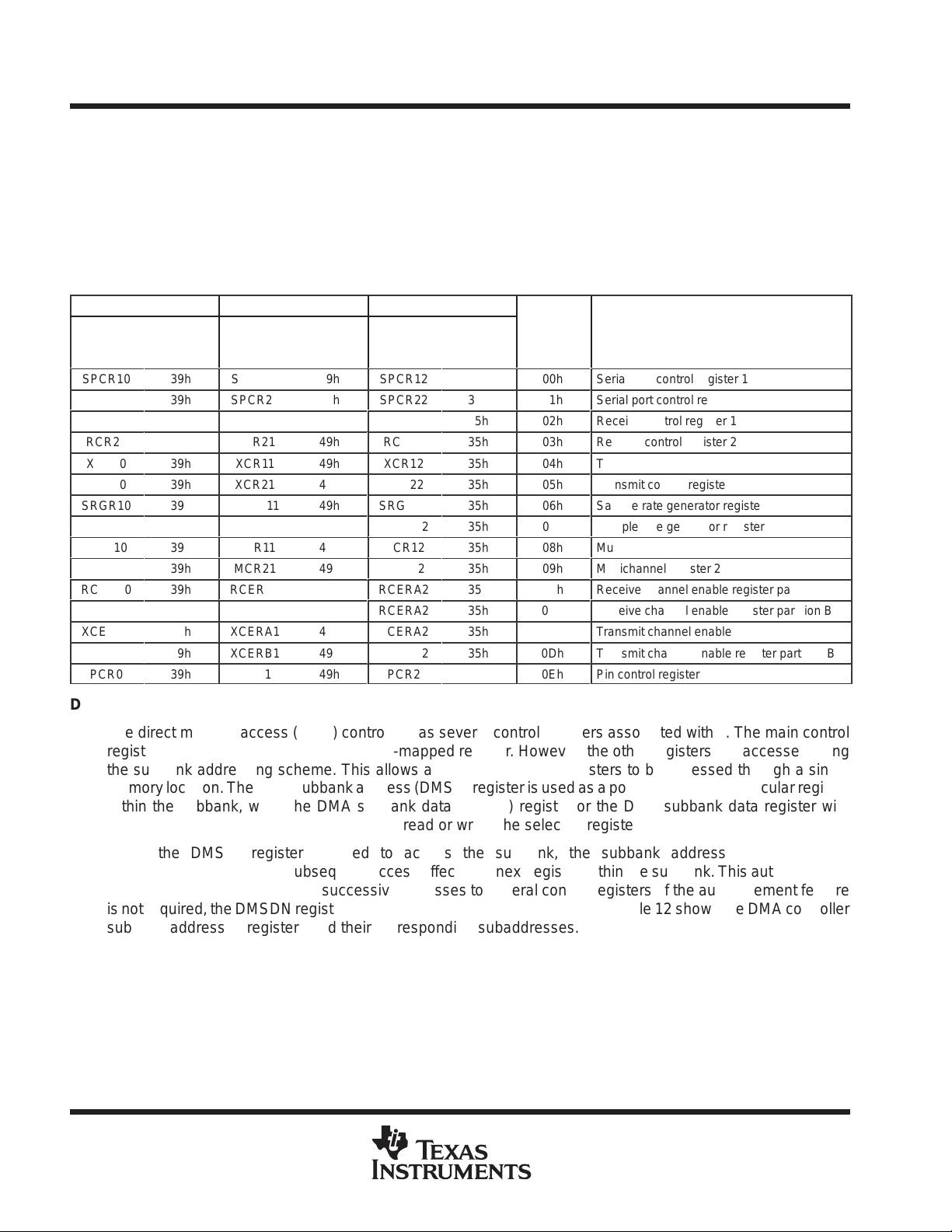
TMS320VC5420
FIXED-POINT DIGITAL SIGNAL PROCESSOR
SPRS080C – MARCH 1999 – REVISED APRIL 2000
McBSP control registers and subaddresses
The control registers for the multichannel buffered serial port (McBSP) are accessed using the subbank
addressing scheme. This allows a set or subbank of registers to be accessed through a single memory location.
The McBSP subbank address register (SPSA) is used as a pointer to select a particular register within the
subbank. The McBSP data register (SPSDI) and the DMA autoincrement subaddress register (SPSDN) register
are used to access (read or write) the selected register. Table 1 1 shows the McBSP control registers and their
corresponding subaddresses.
Table 11. McBSP Control Registers and Subaddresses
McBSP0 McBSP1 McBSP2
NAME ADDRESS NAME ADDRESS NAME ADDRESS
SUB-
ADDRESS
DESCRIPTION
SPCR10
SPCR20
RCR10
RCR20
XCR10
XCR20
SRGR10
SRGR20
MCR10
MCR20
RCERA0
RCERB0
XCERA0
XCERB0
PCR0
39h
39h
39h
39h
39h
39h
39h
39h
39h
39h
39h
39h
39h
39h
39h
SPCR11
SPCR21
RCR11
RCR21
XCR11
XCR21
SRGR11
SRGR21
MCR11
MCR21
RCERA1
RCERB1
XCERA1
XCERB1
PCR1
49h
49h
49h
49h
49h
49h
49h
49h
49h
49h
49h
49h
49h
49h
49h
SPCR12
SPCR22
RCR12
RCR22
XCR12
XCR22
SRGR12
SRGR22
MCR12
MCR22
RCERA2
RCERA2
XCERA2
XCERA2
PCR2
35h
35h
35h
35h
35h
35h
35h
35h
35h
35h
35h
35h
35h
35h
35h
00h
01h
02h
03h
04h
05h
06h
07h
08h
09h
0Ah
0Bh
0Ch
0Dh
0Eh
Serial port control register 1
Serial port control register 2
Receive control register 1
Receive control register 2
Transmit control register 1
Transmit control register 2
Sample rate generator register 1
Sample rate generator register 2
Multichannel register 1
Multichannel register 2
Receive channel enable register partition A
Receive channel enable register partition B
Transmit channel enable register partition A
Transmit channel enable register partition B
Pin control register
DMA subbank addressed registers
The direct memory access (DMA) controller has several control registers associated with it. The main control
register (DMPREC) is a standard memory-mapped register. However, the other registers are accessed using
the subbank addressing scheme. This allows a set or subbank of registers to be accessed through a single
memory location. The DMA subbank address (DMSA) register is used as a pointer to select a particular register
within the subbank, while the DMA subbank data (DMSD) register or the DMA subbank data register with
autoincrement (DMSDI) is used to access (read or write) the selected register.
When the DMSDI register is used to access the subbank, the subbank address is automatically
postincremented so that a subsequent access affects the next register within the subbank. This autoincrement
feature is intended for efficient, successive accesses to several control registers. If the autoincrement feature
is not required, the DMSDN register should be used to access the subbank. T able 12 shows the DMA controller
subbank addressed registers and their corresponding subaddresses.
34
POST OFFICE BOX 1443 • HOUSTON, TEXAS 77251–1443
Page 35
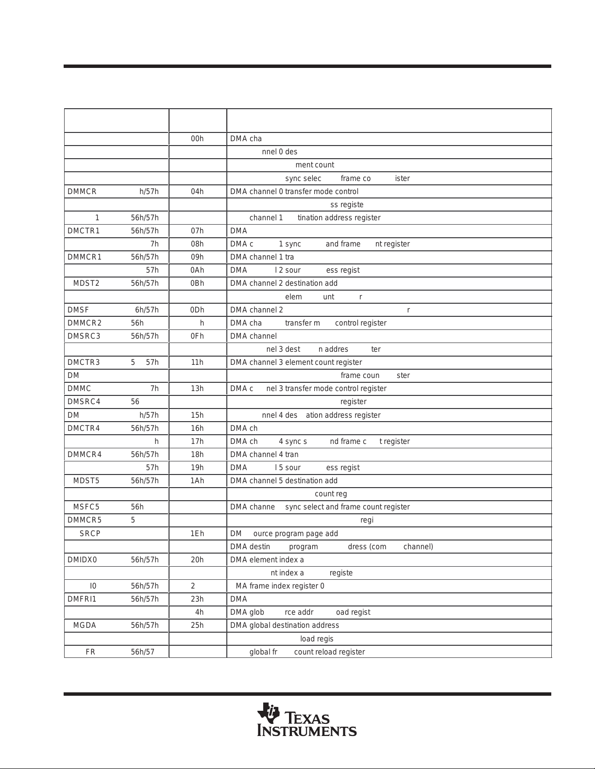
DMA subbank addressed registers (continued)
Table 12. DMA Subbank Addressed Registers
NAME ADDRESS
DMSRC0 56h/57h
DMDST0 56h/57h
DMCTR0 56h/57h
DMSFC0
DMMCR0
DMSRC1
DMDST1
DMCTR1
DMSFC1
DMMCR1
DMSRC2
DMDST2
DMCTR2
DMSFC2
DMMCR2
DMSRC3
DMDST3
DMCTR3
DMSFC3
DMMCR3
DMSRC4
DMDST4
DMCTR4
DMSFC4
DMMCR4
DMSRC5
DMDST5
DMCTR5
DMSFC5
DMMCR5
DMSRCP
DMDSTP
DMIDX0
DMIDX1
DMFRI0
DMFRI1
DMGSA
DMGDA
DMGCR
DMGFR
56h/57h
56h/57h
56h/57h
56h/57h
56h/57h
56h/57h
56h/57h
56h/57h
56h/57h
56h/57h
56h/57h
56h/57h
56h/57h
56h/57h
56h/57h
56h/57h
56h/57h
56h/57h
56h/57h
56h/57h
56h/57h
56h/57h
56h/57h
56h/57h
56h/57h
56h/57h
56h/57h
56h/57h
56h/57h
56h/57h
56h/57h
56h/57h
56h/57h
56h/57h
56h/57h
56h/57h
56h/57h
SUB-
ADDRESS
00h DMA channel 0 source address register
01h DMA channel 0 destination address register
02h DMA channel 0 element count register
03h
04h
05h
06h
07h
08h
09h
0Ah
0Bh
0Ch
0Dh
0Eh
0Fh
10h
11h
12h
13h
14h
15h
16h
17h
18h
19h
1Ah
1Bh
1Ch
1Dh
1Eh
1Fh
20h
21h
22h
23h
24h
25h
26h
27h
DMA channel 0 sync select and frame count register
DMA channel 0 transfer mode control register
DMA channel 1 source address register
DMA channel 1 destination address register
DMA channel 1 element count register
DMA channel 1 sync select and frame count register
DMA channel 1 transfer mode control register
DMA channel 2 source address register
DMA channel 2 destination address register
DMA channel 2 element count register
DMA channel 2 sync select and frame count register
DMA channel 2 transfer mode control register
DMA channel 3 source address register
DMA channel 3 destination address register
DMA channel 3 element count register
DMA channel 3 sync select and frame count register
DMA channel 3 transfer mode control register
DMA channel 4 source address register
DMA channel 4 destination address register
DMA channel 4 element count register
DMA channel 4 sync select and frame count register
DMA channel 4 transfer mode control register
DMA channel 5 source address register
DMA channel 5 destination address register
DMA channel 5 element count register
DMA channel 5 sync select and frame count register
DMA channel 5 transfer mode control register
DMA source program page address (common channel)
DMA destination program page address (common channel)
DMA element index address register 0
DMA element index address register 1
DMA frame index register 0
DMA frame index register 1
DMA global source address reload register
DMA global destination address reload register
DMA global count reload register
DMA global frame count reload register
TMS320VC5420
FIXED-POINT DIGITAL SIGNAL PROCESSOR
SPRS080C – MARCH 1999 – REVISED APRIL 2000
DESCRIPTION
POST OFFICE BOX 1443 • HOUSTON, TEXAS 77251–1443
35
Page 36

TMS320VC5420
NAME
PRIORITY
FUNCTION
FIXED-POINT DIGITAL SIGNAL PROCESSOR
SPRS080C – MARCH 1999 – REVISED APRIL 2000
interrupts
Vector-relative locations and priorities for all internal and external interrupts are shown in Table 13.
Table 13. ’5420 Interrupt Locations and Priorities for Each DSP Subsystem
LOCATION
DECIMAL HEX
RS, SINTR 0 00 1 Reset (Hardware and Software Reset)
NMI, SINT16 4 04 2 Nonmaskable Interrupt
SINT17 8 08 — Software Interrupt #17
SINT18 12 0C — Software Interrupt #18
SINT19 16 10 — Software Interrupt #19
SINT20 20 14 — Software Interrupt #20
SINT21 24 18 — Software Interrupt #21
SINT22 28 1C — Software Interrupt #22
SINT23 32 20 — Software Interrupt #23
SINT24 36 24 — Software Interrupt #24
SINT25 40 28 — Software Interrupt #25
SINT26 44 2C — Software Interrupt #26
SINT27 48 30 — Software Interrupt #27
SINT28 52 34 — Software Interrupt #28
SINT29 56 38 — Software Interrupt #29
SINT30 60 3C — Software Interrupt #30
INT0, SINT0 64 40 3 External User Interrupt #0
INT1, SINT1 68 44 4 External User Interrupt #1
INT2, SINT2 72 48 5 Reserved
TINT, SINT3 76 4C 6 External Timer Interrupt
BRINT0, SINT4 80 50 7 McBSP #0 Receive Interrupt
BXINT0, SINT5 84 54 8 McBSP #0 Transmit Interrupt
BRINT2 (DMAC0),
SINT6
BXINT2 (DMAC1),
SINT7
INT3, SINT8 96 60 11 Reserved
HPINT, SINT9 100 64 12 HPI Interrupt (from DSPINT in HPIC)
BRINT1 (DMAC2),
SINT10
BXINT1 (DMAC3),
SINT11
DMAC4, SINT12 112 70 15 DMA Channel 4
DMAC5, SINT13 116 74 16 DMA Channel 5
IPINT, SINT14 120 78 17 Interprocessor Interrupt
— 124–127 7C–7F — Reserved
88 58 9
92 5C 10
104 68 13
108 6C 14
McBSP #2 Receive Interrupt (default) or DMA
Channel 0 interrupt. The selection is made in
the DMPREC register.
McBSP #2 Receive Interrupt (default) or DMA
Channel 1 interrupt. The selection is made in
the DMPREC register.
McBSP #1 Receive Interrupt (default) or DMA
Channel 2 interrupt. The selection is made in
the DMPREC register.
McBSP #1 transmit Interrupt (default) or DMA
channel 3 interrupt. The selection is made in the
DMPREC register.
36
POST OFFICE BOX 1443 • HOUSTON, TEXAS 77251–1443
Page 37
TMS320VC5420
FIXED-POINT DIGITAL SIGNAL PROCESSOR
SPRS080C – MARCH 1999 – REVISED APRIL 2000
interrupts (continued)
Figure 9 shows the bit layout of the interrupt mask register (IMR) and the interrupt flag register (IFR). T able 14
describes the bit functions.
The interprocessor interrupt (IPINT) bit of the interrupt mask register (IMR) and the interrupt flag register (IFR)
allows the subsystem to perform interrupt service routines based on the other subsystem activity. Incoming
IPINT interrupts are latched in bit 14 of the IFR. Generating an interprocessor interrupt is performed by writing
a “1” to the IPIRQ field of the bank-switching control register (BSCR). Subsequent interrupts must first clear the
interrupt by writing “0” to the IPIRQ field.
For example, if subsystem A is required to notify subsystem B of a completed task, subsystem A must write a
“1” to the IPIRQ field to generate a IPINT interrupt on subsystem B. On subsystem B, the IPINT interrupt is
latched in bit 14 of the IFR.
1514131211109876543210
IPINT DMAC5 DMAC4 BXINT1
RES
Figure 9. Bit Layout of the IMR and IFR Registers for Each Subsystem
DMAC3
BRINT1
or
DMAC2
HPINT RES BXINT2
or
or
DMAC1
BRINT2
or
DMAC0
BXINT0 BRINT0 TINT RES INT1 INT0
Table 14. Bit Functions for IMR and IFR Registers for Each DSP Subsystem
BIT
NUMBER NAME
15 – Reserved
14 IPINT
13 DMAC5 DMA channel 5 interrupt flag/mask bit
12 DMAC4
11 BXINT1/DMAC3
10 BRINT1/DMAC2
9 HPINT
8 –
7 BXINT2/DMAC1
6 BRINT2/DMAC0
5 BXINT0
4 BRINT0
3 TINT
2 –
1 INT1
0 INT0
Interprocessor IRQ.
DMA channel 4 interrupt flag/mask bit
This bit can be configured as either the McBSP1 transmit interrupt flag/mask bit, or the DMA
channel 3 interrupt flag/mask bit. The selection is made in the DMPREC register.
This bit can be configured as either the McBSP1 receive interrupt flag/mask bit, or the DMA
channel 2 interrupt flag/mask bit. The selection is made in the DMPREC register.
Host to ’54x interrupt flag/mask
Reserved
This bit can be configured as either the McBSP2 transmit interrupt flag/mask bit, or the DMA
channel 1 interrupt flag/mask bit. The selection is made in the DMPREC register.
This bit can be configured as either the McBSP2 receive interrupt flag/mask bit, or the DMA
channel 0 interrupt flag/mask bit. The selection is made in the DMPREC register.
McBSP0 transmit interrupt flag/mask bit
McBSP0 receive interrupt flag/mask bit
Timer interrupt flag/mask bit
Reserved
External interrupt 1 flag/mask bit
External interrupt 0 flag/mask bit
FUNCTION
POST OFFICE BOX 1443 • HOUSTON, TEXAS 77251–1443
37
Page 38

TMS320VC5420
FIXED-POINT DIGITAL SIGNAL PROCESSOR
SPRS080C – MARCH 1999 – REVISED APRIL 2000
IDLE3 power-down mode
The IDLE1 and IDLE2 power-down modes operate as described in the
Volume 1: CPU and Peripherals
circuitry is shut off to conserve power . The ’5420 cannot enter an IDLE3 mode unless both subsystems execute
an IDLE3 instruction. The power-reduced benefits of IDLE3 cannot be realized until both subsystems enter the
IDLE3 state and the internal clocks are automatically shut off. The order in which subsystems enter IDLE3 does
not matter.
(literature number SPRU131). The IDLE3 mode is special in that the clocking
TMS320C54x DSP Reference Set,
emulating the ’5420 device
The ’5420 is a single device, but actually consists of two independent subsystems that contain register/status
information used by the emulator tools. The emulator tools must be informed of the multicore device by
modifying the board.cfg file. The board.cfg file is an ASCII file that can be modified with most editors. This
provides the emulator with a description of the JT AG chain. The board.cfg file must identify two processors when
using the ’5420. The file contents would look something like this:
“CPU_B” TI320C5xx
“CPU_A” TI320C5xx
Use the compose program to make this file into a binary file (board.dat), readable by the emulation tools. Place
the board.dat file in the directory that contains the emulator software.
The subsystems are serially connected together internally . Emulation information is serially transmitted into the
device using TDI. The device responds with serial scan information transmitted out the TDO pin.
38
POST OFFICE BOX 1443 • HOUSTON, TEXAS 77251–1443
Page 39

TMS320VC5420
FIXED-POINT DIGITAL SIGNAL PROCESSOR
SPRS080C – MARCH 1999 – REVISED APRIL 2000
documentation support
Extensive documentation supports all TMS320 family generations of devices from product announcement
through applications development. The following types of documentation are available to support the design
and use of the ’C5000 family of DSPs:
TMS320C5000 DSP Family Functional Overview
Device-specific data sheets (such as this document)
Complete User Guides
Development-support tools
Hardware and software application reports
(literature number SPRU307)
The five-volume
Volume 1: CPU and Peripherals
Volume 2: Mnemonic Instruction Set
Volume 3: Algebraic Instruction Set
Volume 4: Applications Guide
Volume 5: Enhanced Peripherals
The reference set describes in detail the ’54x TMS320 products currently available and the hardware and
software applications, including algorithms, for fixed-point TMS320 devices.
For general background information on DSPs and Texas Instruments (TI) devices, see the three-volume
publication
SPRA016, and SPRA017).
A series of DSP textbooks is published by Prentice-Hall and John Wiley & Sons to support digital signal
processing research and education. The TMS320 newsletter,
quarterly and distributed to update TMS320 customers on product information.
Information regarding TI DSP products is also available on the Worldwide Web at
resource locator (URL).
TMS320C54x DSP Reference Set
(literature number SPRU131)
(literature number SPRU172)
(literature number SPRU179)
(literature number SPRU173)
(literature number SPRU302)
Digital Signal Processing Applications with the TMS320 Family
(literature number SPRU210) consists of:
Details on Signal Processing
(literature numbers SPRA012,
, is published
http://www.ti.com
uniform
TI is a trademark of Texas Instruments Incorporated.
POST OFFICE BOX 1443 • HOUSTON, TEXAS 77251–1443
39
Page 40
TMS320VC5420
VIHHigh level in ut voltage, I/O
V
VILLow level in ut voltage, I/O
V
FIXED-POINT DIGITAL SIGNAL PROCESSOR
SPRS080C – MARCH 1999 – REVISED APRIL 2000
absolute maximum ratings over specified temperature range (unless otherwise noted)
Supply voltage I/O range, DV
Supply voltage core range, CV
Supply voltage analog PLL, AV
Input voltage range, VI – 0.5 V to DV
‡
– 0.5 V to 4.0 V. . . . . . . . . . . . . . . . . . . . . . . . . . . . . . . . . . . . . . . . . . . . . . . . . .
DD
‡
– 0.5 V to 2.0 V. . . . . . . . . . . . . . . . . . . . . . . . . . . . . . . . . . . . . . . . . . . . . . . . .
DD
‡
– 0.5 V to 2.0 V. . . . . . . . . . . . . . . . . . . . . . . . . . . . . . . . . . . . . . . . . . . . . . . . .
DD
†
DD
+ 0.5 V. . . . . . . . . . . . . . . . . . . . . . . . . . . . . . . . . . . . . . . . . . . . . . . . . . . .
Output voltage range, Vo – 0.5 V to DVDD + 0.5 V. . . . . . . . . . . . . . . . . . . . . . . . . . . . . . . . . . . . . . . . . . . . . . . . . .
Operating case temperature range, T
Storage temperature range T
†
Stresses beyond those listed under “absolute maximum ratings” may cause permanent damage to the device. These are stress ratings only, and
functional operation of the device at these or any other conditions beyond those indicated under “recommended operating conditions” is not
implied. Exposure to absolute-maximum-rated conditions for extended periods may affect device reliability.
‡
All voltage values are with respect to VSS.
– 65C to 150C. . . . . . . . . . . . . . . . . . . . . . . . . . . . . . . . . . . . . . . . . . . . . . . . . . .
stg
– 40°C to 100°C. . . . . . . . . . . . . . . . . . . . . . . . . . . . . . . . . . . . . . . . . . . .
C
recommended operating conditions
MIN NOM MAX UNIT
DV
CV
AV
V
V
V
I
OH
I
OL
T
DD
DD
DD
SS
C
Device supply voltage, I/O 3.0 3.3 3.6 V
Device supply voltage, core 1.71 1.80 1.98 V
Device supply voltage, PLL 1.71 1.80 1.98 V
Supply voltage, GND 0 V
Schmitt trigger inputs, TRST, SELA/B
DV
= 3.3 ± 0.3 V
High-level input voltage, I/O
Low-level input voltage, I/O
High-level output current –300 µA
Low-level output current 1.5 mA
Operating case temperature, industrial –40 100
Operating case temperature, commercial 0 85
DD
All other inputs 2 DV
Schmitt trigger inputs
DV
= 3.3 ± 0.3 V
DD
All other inputs 0 0.8
0.7DV
DD
0 0.3DV
DV
DD
DD
DD
°
°C
V
V
Refer to Figure 10 for 3.3-V device test load circuit values.
40
POST OFFICE BOX 1443 • HOUSTON, TEXAS 77251–1443
Page 41
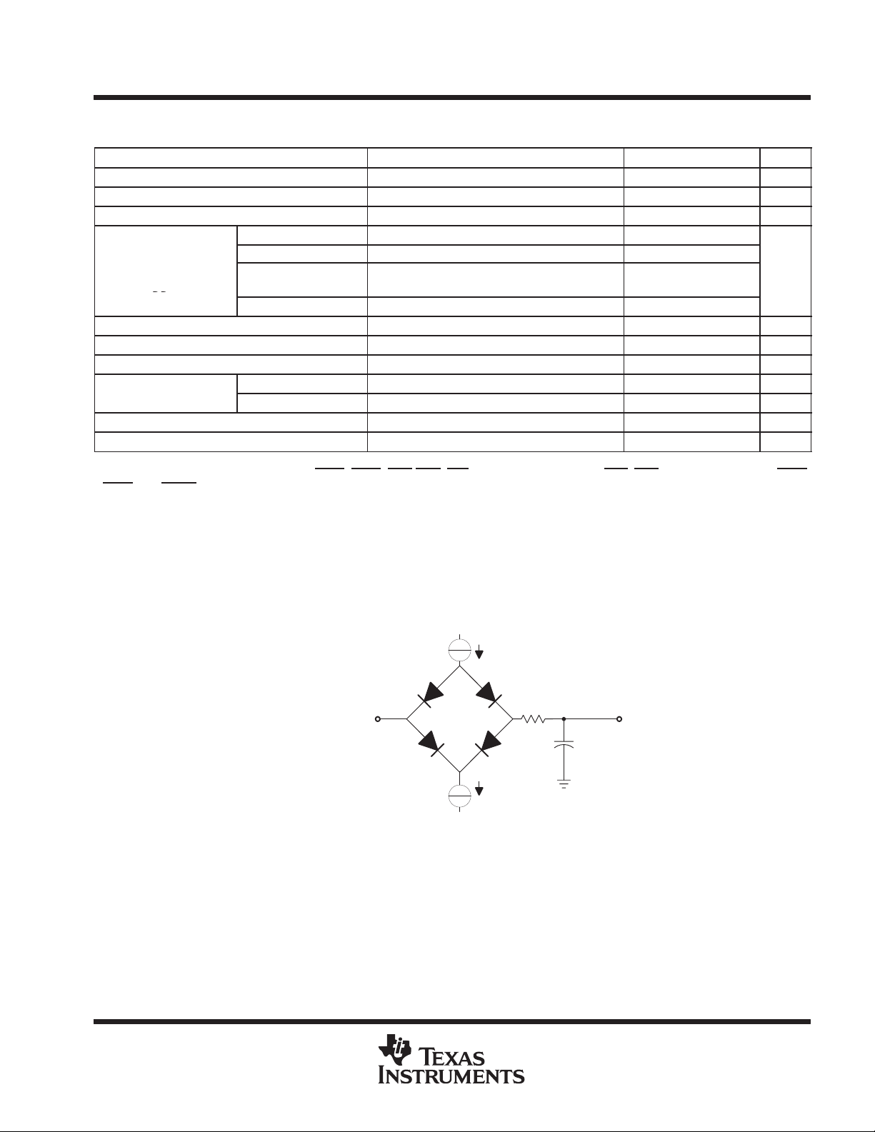
TMS320VC5420
In ut current
DD
)
Su ly current
FIXED-POINT DIGITAL SIGNAL PROCESSOR
SPRS080C – MARCH 1999 – REVISED APRIL 2000
electrical characteristics over recommended operating case temperature range (unless otherwise
noted)
PARAMETER TEST CONDITIONS MIN TYP†MAX UNIT
V
V
I
IZ
I
I
I
DDC
I
DDP
I
DDA
I
DDC
C
C
†
All values are typical unless otherwise specified.
‡
All input and output voltage levels except A_RS
HDS2
§
Clock mode: PLL × 1 with external source
#
This value represents the current consumption of the CPU, on-chip memory, and on-chip peripherals. Conditions include: program execution
from on-chip RAM, with 50% usage of MAC and 50% usage of NOP instructions. Actual operating current varies with program being executed.
||
This value was obtained using the following conditions: external memory writes at a rate of 20 million writes per second, CLKOFF=0, full-duplex
operation of all six McBSPs at a rate of 10 million bits per second each, and 15-pF loads on all outputs. For more details on how this calculation
is performed, refer to the
High-level output voltage
OH
Low-level output voltage
OL
Input current in high impedance DV
Input current
(VI = VSS to
VDD)
Supply current, both core CPUs CVDD = 1.8 V, fx=100 MHz§, TC=25°C
Supply current, pins
Supply current, PLL 5 mA
Supply current,
standby
Input capacitance 5 pF
i
Output capacitance 5 pF
o
, and HPIRS are LVTTL-compatible.
,
‡
‡
TRST With internal pulldown –10 35
See pin descriptions
PPD[15:0]
All other input-only pins –10 10
IDLE2 PLL × n mode, 20 MHz input 2 mA
IDLE3
Calculation of TMS320C54x Power Dissipation Application Report
DV
= 3.3 ± 0.3 V, I
DD
IOL = MAX 0.4 V
= MAX, V
DD
With internal pullups –35 10
Bus holders enabled, DVDD = MAX,
VI = VSS to VIL (MAX); VIH (MIN) to DV
DVDD = 3.3 V, f
PLL x n mode, 20 MHz input 600 µA
, B_RS, INT0 INT1, NMI, CLKIN, BCLKX, BCLKR, HAS, HCS, TCK, TRST, SELA/B, HDS1,
clock
= MAX 2.4 V
OH
= VSS to DV
O
= 100 MHz¶, TC = 25°C
DD
DD
#
(literature number SPRA164).
–10 10 µA
–200 200
||
180 mA
54 mA
µA
Where: I
PARAMETER MEASUREMENT INFORMATION
Tester Pin
Electronics
= 1.5 mA (all outputs)
OL
I
= 300 µA (all outputs)
OH
V
= 1.5 V
Load
C
= 40 pF typical load circuit capacitance
T
I
OL
V
Load
I
OH
Figure 10. 3.3-V Test Load Circuit
50 Ω
Output
Under
C
Test
T
POST OFFICE BOX 1443 • HOUSTON, TEXAS 77251–1443
41
Page 42

TMS320VC5420
)
t
c(CI)
Cycle time, CLKIN
ns
FIXED-POINT DIGITAL SIGNAL PROCESSOR
SPRS080C – MARCH 1999 – REVISED APRIL 2000
external multiply-by-N clock option
An external frequency can be used by injecting the frequency directly into CLKIN. This external frequency is
multiplied by N to generate the internal machine cycle.
The external frequency injected must conform to specifications listed in the timing requirements table.
switching characteristics over recommended operating conditions [H = 0.5t
and the recommended operating conditions table)
PARAMETER MIN TYP MAX UNIT
t
c(CO)
t
d(CIH-CO)
t
f(CO)
t
r(CO)
t
w(COL)
t
w(COH)
t
p
†
N is the PLL multiplier. N = 1 – 15
Cycle time, CLKOUT 10 t
Delay time, CLKIN high/low to CLKOUT high/low 4 10 16 ns
Fall time, CLKOUT 2 ns
Rise time, CLKOUT 2 ns
Pulse duration, CLKOUT low H – 2 H – 1 H ns
Pulse duration, CLKOUT high H – 2 H – 1 H ns
Transitory phase, PLL lock-up time 35 µs
timing requirements (see Figure 11)
Integer PLL multiplier N 10N 200
t
c(CI
t
f(CI)
t
r(CI)
Cycle time, CLKIN
Fall time, CLKIN 8 ns
Rise time, CLKIN 8 ns
t
c(CI)
PLL multiplier N = x.5
PLL multiplier N = x.25, x.75 10N 50
t
r(CI)
] (see Figure 11
c(CO)
†
c(CI)/N
MIN MAX UNIT
10N 100
t
f(CI)
ns
ns
CLKIN
CLKOUT
t
tp
Unstable
d(CI-CO)
t
c(CO)
t
w(COH)
Figure 11. External Multiply-By-One Clock
t
f(CO)
t
w(COL)
t
r(CO)
42
POST OFFICE BOX 1443 • HOUSTON, TEXAS 77251–1443
Page 43
FIXED-POINT DIGITAL SIGNAL PROCESSOR
SPRS080C – MARCH 1999 – REVISED APRIL 2000
bypass option
An external frequency can be used by injecting the frequency directly into CLKIN.
The external frequency injected must conform to specifications listed in the timing requirements table.
TMS320VC5420
switching characteristics over recommended operating conditions [H = 0.5t
and the recommended operating conditions table)
PARAMETER MIN TYP MAX UNIT
t
c(CO)
t
d(CIH-CO)
t
f(CO)
t
r(CO)
t
w(COL)
t
w(COH)
Cycle time, CLKOUT 10 t
Delay time, CLKIN high/low to CLKOUT high/low 4 10 16 ns
Fall time, CLKOUT 2 ns
Rise time, CLKOUT 2 ns
Pulse duration, CLKOUT low H – 2 H – 1 H ns
Pulse duration, CLKOUT high H – 2 H – 1 H ns
timing requirements (see Figure 11)
t
c(CI)
t
f(CI)
t
r(CI)
†
This device utilizes a fully static design and therefore can operate with t
approaching 0 Hz.
Cycle time, CLKIN 10
Fall time, CLKIN 8 ns
Rise time, CLKIN 8 ns
approaching . The device is characterized at frequencies
c(CI)
t
r(CI)
t
f(CO)
t
w(COL)
CLKIN
CLKOUT
t
c(CI)
Unstable
t
d(CI-CO)
t
c(CO)
t
w(COH)
] (see Figure 11
c(CO)
c(CI)
MIN MAX UNIT
t
f(CI)
t
r(CO)
ns
†
ns
Figure 12. Timing Diagram for Bypass Mode
POST OFFICE BOX 1443 • HOUSTON, TEXAS 77251–1443
43
Page 44

TMS320VC5420
FIXED-POINT DIGITAL SIGNAL PROCESSOR
SPRS080C – MARCH 1999 – REVISED APRIL 2000
external memory interface timing for one wait state
switching characteristics over recommended operating conditions for a one-wait-state memory
read (MSTRB
= 0)† (see Figure 13)
PARAMETER MIN MAX
t
d(CLKL-A)
t
d(CLKH-A)
t
d(CLKL-MSL)
t
d(CLKL-MSH)
t
h(CLKL-A)R
t
h(CLKH-A)R
†
Address, PS, and DS timings are all included in timings referenced as address.
‡
In the case of a memory read preceded by a memory read
§
In the case of a memory read preceded by a memory write
Delay time, CLKOUT low to address valid
Delay time, CLKOUT high (transition) to address valid
Delay time, CLKOUT low to MSTRB low –1 4 ns
Delay time, CLKOUT low to MSTRB high –1 4 ns
Hold time, address valid after CLKOUT low
Hold time, address valid after CLKOUT high
‡
§
‡
§
timing requirements for a one-wait-state memory read (MSTRB = 0) [H = 0.5 t
t
a(A)M
t
a(MSTRBL)
t
su(D)R
t
h(D)R
t
h(A-D)R
t
h(D)MSTRBH
†
Address, PS, and DS timings are all included in timings referenced as address.
Access time, read data access from address valid (1 wait state required) 4H–15 ns
Access time, read data access from MSTRB low 4H–14 ns
Setup time, read data before CLKOUT low 12 ns
Hold time, read data after CLKOUT low 0 ns
Hold time, read data after address invalid 0 ns
Hold time, read data after MSTRB high 0 ns
–1 5 ns
–1 6 ns
–1 5 ns
–1 6 ns
]† (see Figure 13)
c(CO)
MIN MAX
UNIT
UNIT
44
POST OFFICE BOX 1443 • HOUSTON, TEXAS 77251–1443
Page 45

FIXED-POINT DIGITAL SIGNAL PROCESSOR
external memory interface timing for one wait state (continued)
CLKOUT
t
d(CLKL-A)
PPA[17:0]
t
su(D)R
t
a(A)M
PPD[15:0]
t
d(CLKL-MSL)
t
a(MSTRBL)
TMS320VC5420
SPRS080C – MARCH 1999 – REVISED APRIL 2000
t
h(CLKL-A)R
t
h(A-D)R
t
h(D)R
t
h(D)MSTRBH
t
d(CLKL-MSH)
MSTRB
R/W
PS, DS
1 Wait State
Figure 13. Memory Read (MSTRB = 0)
POST OFFICE BOX 1443 • HOUSTON, TEXAS 77251–1443
45
Page 46

TMS320VC5420
FIXED-POINT DIGITAL SIGNAL PROCESSOR
SPRS080C – MARCH 1999 – REVISED APRIL 2000
external memory interface timing for a memory write for one wait state
switching characteristics over recommended operating conditions for a memory write
(MSTRB
t
d(CLKH-A)
t
d(CLKL-A)
t
d(CLKL-MSL)
t
d(CLKL-D)W
t
d(CLKL-MSH)
t
d(CLKH-RWL)
t
d(CLKH-RWH)
t
d(RWL-MSTRBL)
t
h(A)W
†
Address, PS
‡
In the case of a memory write preceded by a memory write
§
In the case of a memory write preceded by an I/O cycle.
= 0) [H = 0.5 t
Delay time, CLKOUT high to address valid
Delay time, CLKOUT low to address valid
Delay time, CLKOUT low to MSTRB low –1 4 ns
Delay time, CLKOUT low to data valid 0 12 ns
Delay time, CLKOUT low to MSTRB high – 1 4 ns
Delay time, CLKOUT high to R/W low 0 4 ns
Delay time, CLKOUT high to R/W high –1 4 ns
Delay time, R/W low to MSTRB low H – 2 H + 2 ns
Hold time, address valid after CLKOUT high
, and DS timings are all included in timings referenced as address.
]† (see Figure 14)
c(CO)
PARAMETER MIN MAX UNIT
‡
§
‡
– 1 6 ns
–1 5 ns
–1 6 ns
timing requirements for a memory write (MSTRB = 0) [H = 0.5 t
t
h(D)MSH
t
w(SL)MS
t
su(A)W
t
su(D)MSH
†
Address, PS, and DS timings are all included in timings referenced as address.
§
In the case of a memory write preceded by an I/O cycle.
Hold time, write data valid after MSTRB high H – 3 H +3§ns
Pulse duration, MSTRB low
Setup time, address valid before MSTRB low H–4 ns
Setup time, write data valid before MSTRB high 4H–10 4H+5§ns
§
]† (see Figure 14)
c(CO)
MIN MAX
4H–4 ns
UNIT
46
POST OFFICE BOX 1443 • HOUSTON, TEXAS 77251–1443
Page 47

TMS320VC5420
FIXED-POINT DIGITAL SIGNAL PROCESSOR
SPRS080C – MARCH 1999 – REVISED APRIL 2000
external memory interface timing for a memory write for one wait state (continued)
CLKOUT
t
A[19:0]
D[15:0]
MSTRB
R/W
d(CLKL-A)
t
su(A)W
t
d(CLKH-RWL)
t
d(CLKL-D)W
t
su(D)MSH
t
d(CLKL-MSL)
t
w(SL)MS
t
d(RWL-MSTRBL)
t
h(A)W
t
d(CLKL-MSH)
t
d(CLKH-A)
t
h(D)MSH
t
d(CLKH-RWH)
PS, DS
1 Wait State
Figure 14. Memory Write (MSTRB = 0)
POST OFFICE BOX 1443 • HOUSTON, TEXAS 77251–1443
47
Page 48
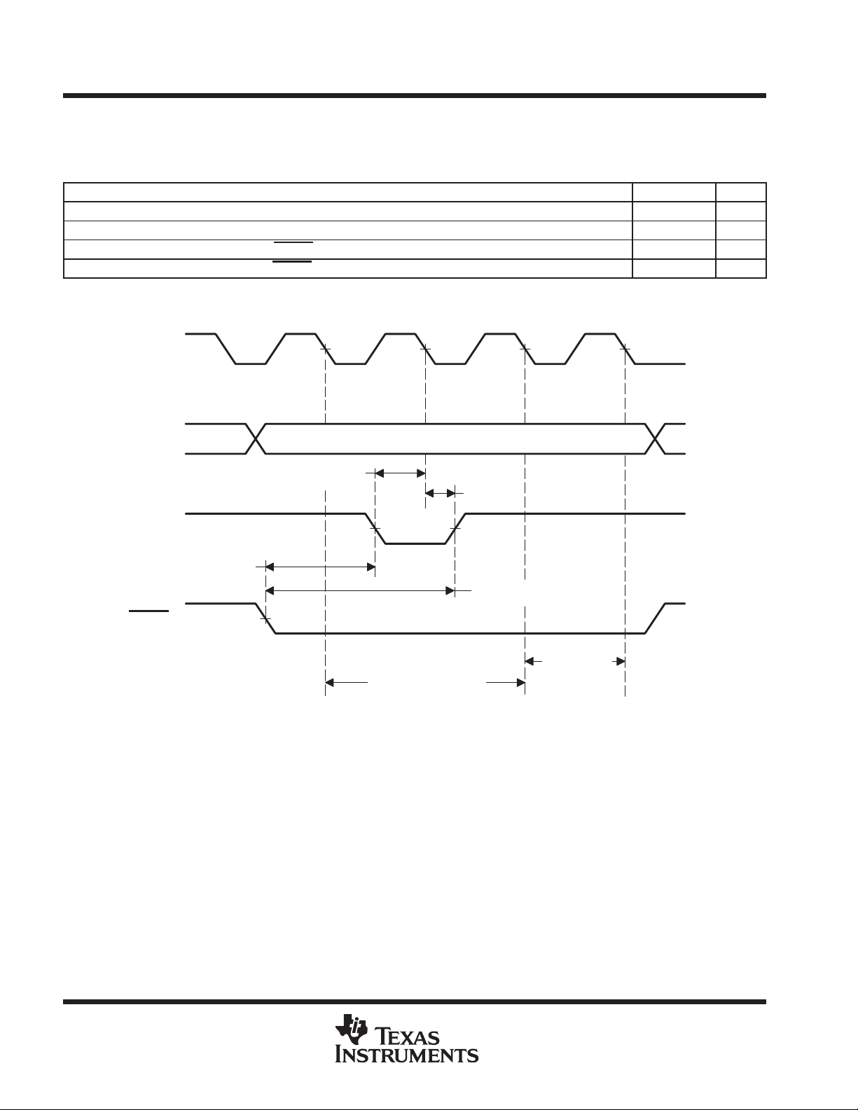
TMS320VC5420
FIXED-POINT DIGITAL SIGNAL PROCESSOR
SPRS080C – MARCH 1999 – REVISED APRIL 2000
ready timing for externally generated wait states
timing requirements for externally generated wait states [H = 0.5 t
]† (see Figure 15 and
c(CO)
Figure 16)
MIN MAX UNIT
t
su(RDY)
t
h(RDY)
t
v(RDY)MSTRB
t
h(RDY)MSTRB
†
The hardware wait states can be used only in conjunction with the software wait states to extend the bus cycles. To generate wait states by
READY , at least two software wait states must be programmed. READY is not sampled until the completion of the internal software wait states.
‡
These timings are included for reference only. The critical timings for READY are those referenced to CLKOUT
Setup time, READY before CLKOUT low 7 ns
Hold time, READY after CLKOUT low 0 ns
Valid time, READY after MSTRB low
Hold time, READY after MSTRB low
CLKOUT
A[19:0]
READY
‡
‡
t
su(RDY)
t
h(RDY)
4H ns
4H–8 ns
MSTRB
t
v(RDY)MSTRB
t
h(RDY)MSTRB
Wait States
Generated Internally
Figure 15. Memory Read With Externally Generated Wait States
Wait State
Generated
by READY
48
POST OFFICE BOX 1443 • HOUSTON, TEXAS 77251–1443
Page 49

FIXED-POINT DIGITAL SIGNAL PROCESSOR
ready timing for externally generated wait states (continued)
CLKOUT
A[19:0]
D[15:0]
t
h(RDY)
t
su(RDY)
READY
t
v(RDY)MSTRB
t
h(RDY)MSTRB
MSTRB
TMS320VC5420
SPRS080C – MARCH 1999 – REVISED APRIL 2000
Wait States
Generated Internally
Figure 16. Memory Write With Externally Generated W ait States
Wait State Generated
by READY
POST OFFICE BOX 1443 • HOUSTON, TEXAS 77251–1443
49
Page 50
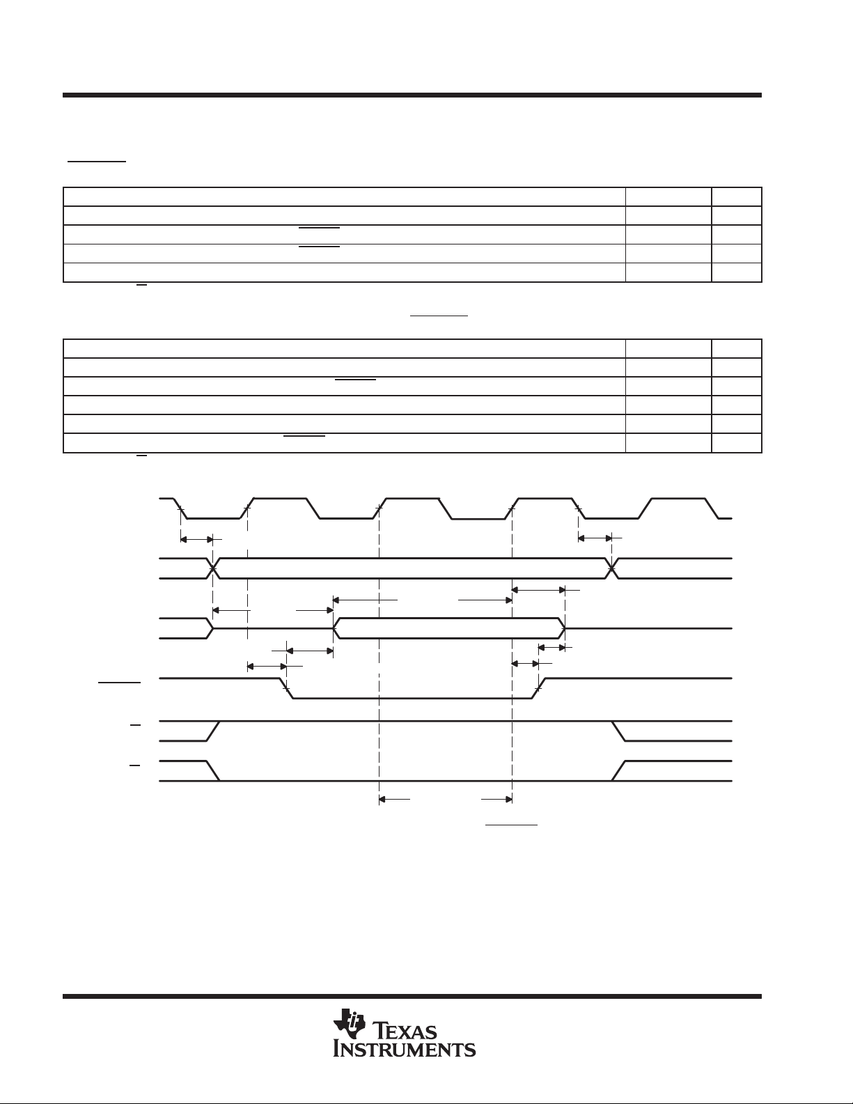
TMS320VC5420
FIXED-POINT DIGITAL SIGNAL PROCESSOR
SPRS080C – MARCH 1999 – REVISED APRIL 2000
parallel I/O interface timing
switching characteristics over recommended operating conditions for a parallel I/O port read
(IOSTRB
t
d(CLKL-A)
t
d(CLKH-ISTRBL)
t
d(CLKH-ISTRBH)
t
h(A)IOR
†
Address and IS timings are included in timings referenced as address.
= 0)† (see Figure 17)
PARAMETER MIN MAX UNIT
Delay time, CLKOUT low to address valid –1 5 ns
Delay time, CLKOUT high to IOSTRB low 0 5 ns
Delay time, CLKOUT high to IOSTRB high 0 5 ns
Hold time, address after CLKOUT low –1 5 ns
timing requirements for a parallel I/O port read (IOSTRB = 0) [H = 0.5 t
t
a(A)IO
t
a(ISTRBL)IO
t
su(D)IOR
t
h(D)IOR
t
h(ISTRBH-D)R
†
Address and IS
CLKOUT
PPA[17:0]
PPD[15:0]
IOSTRB
Access time, read data access from address valid 5H–15 ns
Access time, read data access from IOSTRB low 4H–14 ns
Setup time, read data before CLKOUT high 10 ns
Hold time, read data after CLKOUT high 0 ns
Hold time, read data after IOSTRB high 0 ns
timings are included in timings referenced as address.
t
d(CLKL-A)
t
su(D)IOR
t
t
a(ISTRBL)IO
t
a(A)IO
t
d(CLKH-ISTRBL)
†
]
c(CO)
t
d(CLKH-ISTRBH)
(see Figure 17)
t
h(A)IOR
t
h(D)IOR
h(ISTRBH-D)R
MIN MAX UNIT
50
R/W
IS
1 Wait State
Figure 17. Parallel I/O Port Read (IOSTRB=0)
POST OFFICE BOX 1443 • HOUSTON, TEXAS 77251–1443
Page 51

TMS320VC5420
FIXED-POINT DIGITAL SIGNAL PROCESSOR
SPRS080C – MARCH 1999 – REVISED APRIL 2000
parallel I/O interface timing (continued)
switching characteristics over recommended operating conditions for a parallel I/O port write
(IOSTRB
t
d(CLKL-A)
t
d(CLKH-ISTRBL)
t
d(CLKH-D)IOW
t
d(CLKH-ISTRBH)
t
d(CLKL-RWL)
t
d(CLKL-RWH)
t
h(A)IOW
t
h(D)IOW
t
su(D)IOSTRBH
t
su(A)IOSTRBL
†
Address and IS
CLKOUT
= 0) [H = 0.5 t
Delay time, CLKOUT low to address valid –1 5 ns
Delay time, CLKOUT high to IOSTRB low 0 5 ns
Delay time, CLKOUT high to write data valid H–5 H+11 ns
Delay time,CLKOUT high to IOSTRB high 0 5 ns
Delay time, CLKOUT low to R/W low 0 4 ns
Delay time, CLKOUT low to R/W high 0 4 ns
Hold time, address valid after CLKOUT low –1 5 ns
Hold time, write data after IOSTRB high H–3 H+5 ns
Setup time, write data before IOSTRB high 3H–9 3H+5 ns
Setup time, address valid before IOSTRB low H–3 H+3 ns
timings are included in timings referenced as address.
]† (see Figure 18)
c(CO)
PARAMETER MIN MAX UNIT
t
d(CLKL-A)
PPA[17:0]
PPD[15:0]
IOSTRB
R/W
t
d(CLKH-D)IOW
t
d(CLKH-ISTRBL)
IS
t
d(CLKL-RWL)
t
su(A)IOSTRBL
t
d(CLKH-ISTRBH)
t
su(D)IOSTRBH
1 Wait State
Figure 18. Parallel I/O Port Write (IOSTRB=0)
t
t
h(D)IOW
t
d(CLKL-RWH)
h(A)IOW
POST OFFICE BOX 1443 • HOUSTON, TEXAS 77251–1443
51
Page 52
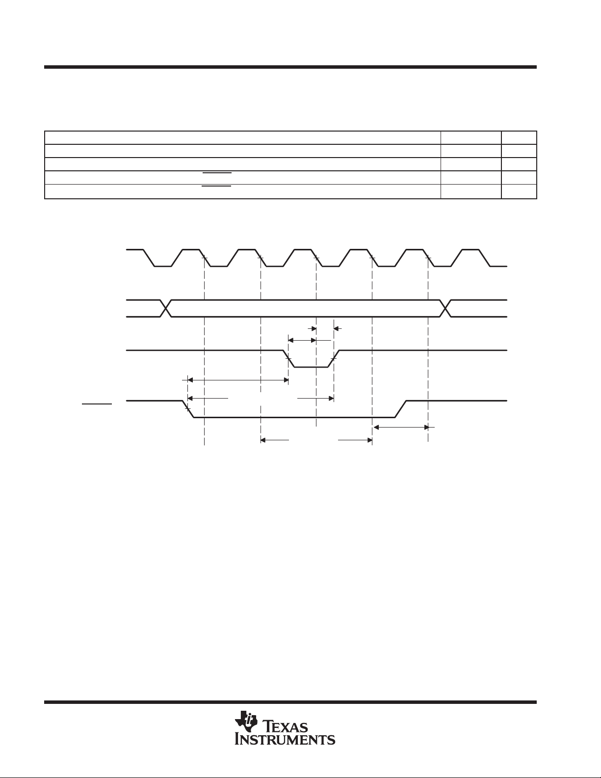
TMS320VC5420
FIXED-POINT DIGITAL SIGNAL PROCESSOR
SPRS080C – MARCH 1999 – REVISED APRIL 2000
ready timing for externally generated wait states
timing requirements for externally generated wait states [H = 0.5 t
]† (see Figure 19 and
c(CO)
Figure 20)
MIN MAX UNIT
t
su(RDY)
t
h(RDY)
t
v(RDY)IOSTRB
t
h(RDY)IOSTRB
†
The hardware wait states can be used only in conjunction with the software wait states to extend the bus cycles. To generate wait states using
READY, at least two software wait states must be programmed.
‡
These timings are included for reference only. The critical timings for READY are those referenced to CLKOUT.
CLKOUT
PPA[17:0]
READY
IOSTRB
Setup time, READY before CLKOUT low 7 ns
Hold time, READY after CLKOUT low 0 ns
Valid time, READY after IOSTRB low
Hold time, READY after IOSTRB low
t
v(RDY)IOSTRB
‡
‡
t
t
h(RDY)IOSTRB
h(RDY)
Generated
Internally
Wait
States
t
su(RDY)
5H–8 ns
5H ns
Wait State Generated
by READY
52
Figure 19. I/O Port Read With Externally Generated Wait States
POST OFFICE BOX 1443 • HOUSTON, TEXAS 77251–1443
Page 53

FIXED-POINT DIGITAL SIGNAL PROCESSOR
ready timing for externally generated wait states (continued)
CLKOUT
PPA[17:0]
D[15:0]
t
h(RDY)
t
su(RDY)
READY
t
v(RDY)IOSTRB
t
h(RDY)IOSTRB
IOSTRB
Wait States
Generated
Internally
TMS320VC5420
SPRS080C – MARCH 1999 – REVISED APRIL 2000
Wait State Generated
by READY
Figure 20. I/O Port Write With Externally Generated W ait States
POST OFFICE BOX 1443 • HOUSTON, TEXAS 77251–1443
53
Page 54
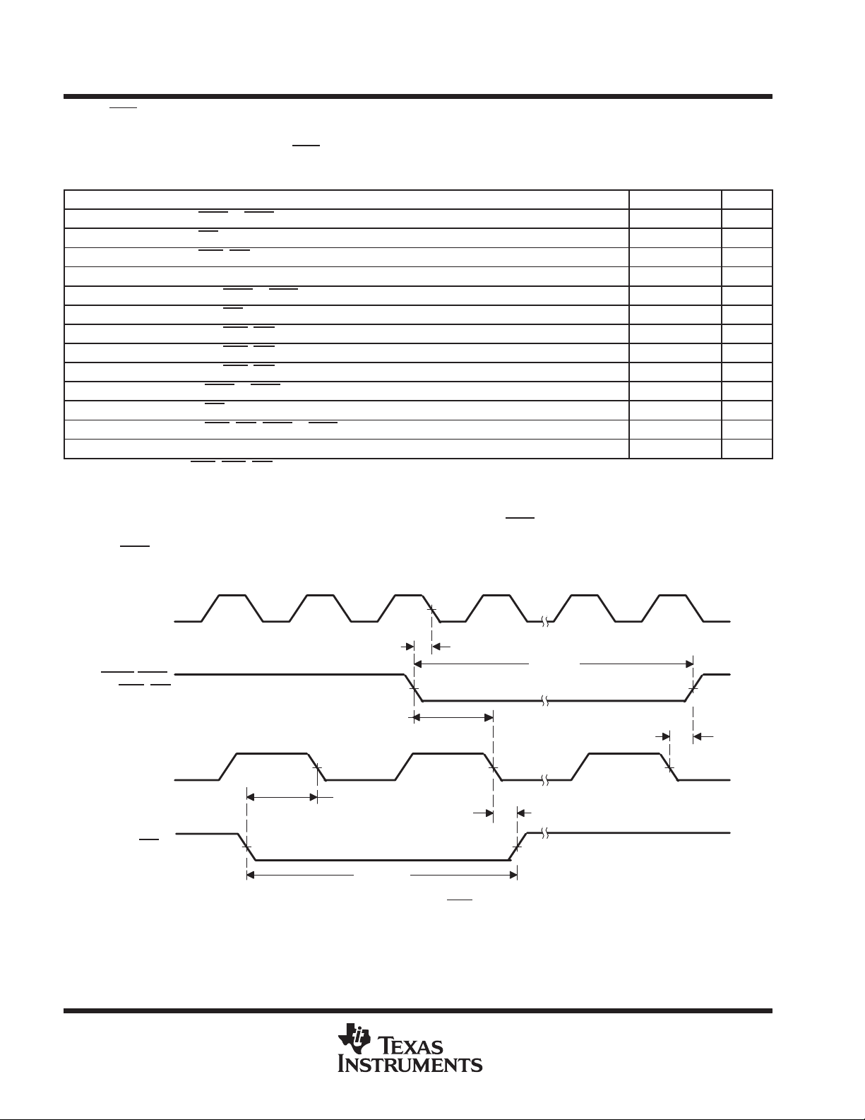
TMS320VC5420
FIXED-POINT DIGITAL SIGNAL PROCESSOR
SPRS080C – MARCH 1999 – REVISED APRIL 2000
reset, BIO, interrupt, and XIO timing
timing requirements for reset, BIO, interrupt, and XIO [H = 0.5 t
] (see Figure 21, Figure 22,
c(CO)
and Figure 23)
MIN MAX UNIT
t
h(RS)
t
h(BIO)
t
h(INT)
t
h(XIO)
t
w(RSL)
t
w(BIO)A
t
w(INTH)A
t
w(INTL)A
t
w(INTL)WKP
t
su(RS)
t
su(BIO)
t
su(INT)
t
su(XIO)
†
The external interrupts (INT0–INT1, NMI) are synchronized to the core CPU by way of a two flip-flop synchronizer which samples these inputs
with consecutive falling edges of CLKOUT. The input to the interrupt pins is required to represent a 1-0-0 sequence at the timing that is
corresponding to a three-CLKOUT sampling sequence.
‡
Once the setup and hold times are met for XIO, the following falling edge of CLKOUT is either an HPI or EMIF cycle.
§
If the PLL mode is selected, then at power-on sequence, or at wakeup from IDLE3, A_RS
synchronization and lock-in of the PLL.
¶
Note that A_RS
(PLL
) section).
Hold time, A_RS or B_RS after CLKOUT low 0 ns
Hold time, BIO after CLKOUT low 0 ns
§¶
†
4H+5 ns
†
†
†
¶
†
must be held low for at least 50 µs to ensure
software-programmable phase-locked loop
4H ns
4H ns
Hold time, INTn, NMI, after CLKOUT low
‡
Hold time, XIO after CLKOUT low 0 ns
Pulse duration, A_RS or B_RS low
Pulse duration, BIO low, asynchronous 5H ns
Pulse duration, INTn, NMI high (asynchronous)
Pulse duration, INTn, NMI low (asynchronous)
Pulse duration, INTn, NMI low for IDLE2/IDLE3 wakeup
Setup time, A_RS or B_RS before CLKIN low
Setup time, BIO before CLKOUT low 9 ns
Setup time, INTn, NMI, A_RS or B_RS before CLKOUT low
‡
Setup time, XIO before CLKOUT low 10 ns
can cause a change in clock frequency, therefore changing the value of H (see the
0 ns
8 ns
7 ns
9 ns
CLKIN
A_RS,
INTn
CLKOUT
B_RS,
, NMI
BIO
t
su(RS)
t
su(INT)
t
su(BIO)
t
w(BIO)S
Figure 21. Reset and BIO Timings
t
w(RSL)
t
h(BIO)
t
h(RS)
54
POST OFFICE BOX 1443 • HOUSTON, TEXAS 77251–1443
Page 55
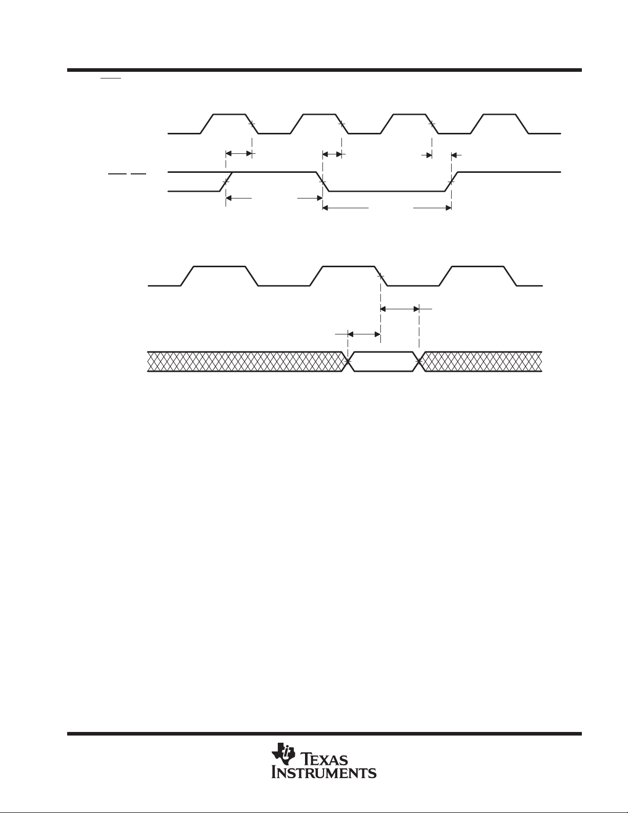
reset, BIO, interrupt, and XIO timing (continued)
CLKOUT
TMS320VC5420
FIXED-POINT DIGITAL SIGNAL PROCESSOR
SPRS080C – MARCH 1999 – REVISED APRIL 2000
INTn, NMI
CLKOUT
XIO
t
su(INT)
t
w(INTH)A
t
su(INT)
t
Figure 22. Interrupt Timing
t
su(XIO)
Figure 23. XIO Timing
w(INTL)A
t
h(XIO)
t
h(INT)
POST OFFICE BOX 1443 • HOUSTON, TEXAS 77251–1443
55
Page 56

TMS320VC5420
FIXED-POINT DIGITAL SIGNAL PROCESSOR
SPRS080C – MARCH 1999 – REVISED APRIL 2000
external flag (XF), and timer output (TOUT) timing
switching characteristics over recommended operating conditions for external flag (XF) and TOUT
[H = 0.5 t
t
d(XF)
t
d(TOUTH)
t
d(TOUTL)
t
w(TOUT)
CLKOUT
] (see Figure 24 and Figure 25)
c(CO)
PARAMETER MIN MAX UNIT
Delay time, CLKOUT low to XF high 0 3
Delay time, CLKOUT low to XF low 0 3
Delay time, CLKOUT high to TOUT high 0 5 ns
Delay time, CLKOUT high to TOUT low 0 5 ns
Pulse duration, TOUT 2H–2 ns
t
d(XF)
XF
ns
CLKOUT
TOUT
t
d(TOUTH)
Figure 24. External Flag (XF) Timing
t
d(TOUTL)
t
w(TOUT)
Figure 25. Timer (TOUT) Timing
56
POST OFFICE BOX 1443 • HOUSTON, TEXAS 77251–1443
Page 57

general purpose input output (GPIO) timing
timing requirements for GPIO (see Figure 26)
t
su(GPIO-COH)
t
h(GPIO-COH)
Setup time, GPIOx input valid before CLKOUT high, GPIOx configured as
general-purpose input.
Hold time, GPIOx input valid after CLKOUT high, GPIOx configured as general-purpose
input.
switching characteristics for GPIO (see Figure 26)
PARAMETER MIN MAX UNIT
t
d(COH-GPIO)
Delay time, CLKOUT high to GPIOx output change. GPIOx configured as
general-purpose output.
CLKOUT
TMS320VC5420
FIXED-POINT DIGITAL SIGNAL PROCESSOR
SPRS080C – MARCH 1999 – REVISED APRIL 2000
MIN MAX UNIT
7 ns
0 ns
0 5 ns
GPIOx Input Mode
GPIOx Output Mode
t
d(COH-GPIO)
Figure 26. GPIO Timings
t
su(GPIO-COH)
t
h(GPIO-COH)
POST OFFICE BOX 1443 • HOUSTON, TEXAS 77251–1443
57
Page 58
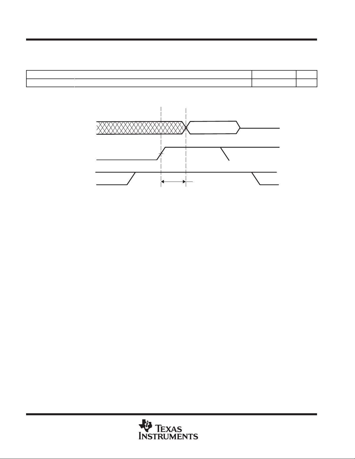
TMS320VC5420
FIXED-POINT DIGITAL SIGNAL PROCESSOR
SPRS080C – MARCH 1999 – REVISED APRIL 2000
SELA/B timing
switching characteristics in XIO = 1 mode for SELA/B (see Figure 27)
PARAMETER MIN MAX UNIT
t
d(SELA/B-ABUS)
Delay time, SELA/B to address bus valid in XIO = 1 mode. 3 10 ns
PPA[17:0]
SELA/B
XIO
VALID A BUS
t
d(SELA/B-ABUS)
Figure 27. SELA/B Timing in XIO = 1 Mode
58
POST OFFICE BOX 1443 • HOUSTON, TEXAS 77251–1443
Page 59
multichannel buffered serial port timing
TMS320VC5420
FIXED-POINT DIGITAL SIGNAL PROCESSOR
SPRS080C – MARCH 1999 – REVISED APRIL 2000
timing requirements for the McBSP† [H=0.5t
t
c(BCKRX)
t
w(BCKRX)
t
h(BCKRL-BFRH)
t
h(BCKRL-BDRV)
t
h(BCKXL-BFXH)
t
su(BFRH-BCKRL)
t
su(BDRV-BCKRL)
t
su(BFXH-BCKXL)
t
r(BCKRX)
t
f(BCKRX)
†
Polarity bits CLKRP = CLKXP = FSRP = FSXP = 0. If the polarity of any of the signals is inverted, then the timing references of that signal are
also inverted.
Cycle time, BCLKR/X BCLKR/X ext 4H ns
Pulse duration, BCLKR/X or BCLKR/X high BCLKR/X ext 6 ns
Hold time, external BFSR high after BCLKR low
Hold time, BDR valid after BCLKR low
Hold time, external BFSX high after BCLKX low
Setup time, external BFSR high before BCLKR low
Setup time, BDR valid before BCLKR low
Setup time, external BFSX high before BCLKX low
Rise time, BCKR/X BCLKR/X ext 8 ns
Fall time, BCKR/X BCLKR/X ext 8 ns
] (see Figure 28 and Figure 29)
c(CO)
BCLKR int 0
BCLKR ext
BCLKR int 0
BCLKR ext
BCLKX int 0
BCLKX ext
BCLKR int 10
BCLKR ext
BCLKR int 10
BCLKR ext
BCLKX int 10
BCLKX ext
MIN MAX UNIT
4
5
4
4
3
6
ns
ns
ns
ns
ns
ns
POST OFFICE BOX 1443 • HOUSTON, TEXAS 77251–1443
59
Page 60

TMS320VC5420
Delay time, BCLKX high to BDX valid. This a lies to all bits exce t the first
(
0b)
des
or 2 (XDATDLY=01b or 10b) modes
(
or 2 (XDATDLY=01b or 10b) modes
(
00b)
(XDATDLY=00b) mode
(
00b)
de
(XDATDLY=00b) mode
FIXED-POINT DIGITAL SIGNAL PROCESSOR
SPRS080C – MARCH 1999 – REVISED APRIL 2000
multichannel buffered serial port timing (continued)
†
mo
[H=0.5t
§
§
§
§
] (see Figure 28 and Figure 29)
c(CO)
BCLKX int –3 8
BCLKX ext
BCLKX int –8 5
BCLKX ext
BCLKX int 0 11
BCLKX ext 5 20
DXENA = 0
DXENA = 1
DXENA = 0
DXENA = 1
DXENA = 0
DXENA = 1
DXENA = 0
DXENA = 1
(literature number SPRU302) for a description of the DX enable (DXENA)
BCLKX int 11
BCLKX ext 20
BCLKX int 25
BCLKX ext 27
BCLKX int –4
BCLKX ext 2
BCLKX int 6
BCLKX ext 12
BFSX int 9
BFSX ext 12
BFSX int 25
BFSX ext 26
BFSX int –1
BFSX ext 2
BFSX int 9
BFSX ext 13
2 15
1 19
switching characteristics for the McBSP
PARAMETER MIN MAX UNIT
t
c(BCKRX)
t
w(BCKRXH)
t
w(BCKRXL)
t
d(BCKRH-BFRV)
t
d(BCKXH-BFXV)
t
dis(BCKXH-BDXHZ)
t
d(BCKXH-BDXV)
t
e(BCKXH-BDX)
t
d(BFXH-BDXV)
t
e(BFXH-BDX)
†
Polarity bits CLKRP = CLKXP = FSRP = FSXP = 0. If the polarity of any of the signals is inverted, then the timing references of
also inverted.
‡
T=BCLKRX period = (1 + CLKGDV) * 2H
C=BCLKRX low pulse width = T/2 when CLKGDV is odd or zero and = (CLKGDV/2) * 2H when CLKGDV is even
D=BCLKRX high pulse width = T/2 when CLKGDV is odd or zero and = (CLKGDV/2 + 1) * 2H when CLKGDV is even
§
See the
TMS320C54x Enhanced Peripherals Reference Set, Volume 5
and data delay features of the McBSP.
Cycle time, BCLKR/X BCLKR/X int 4H ns
Pulse duration, BCLKR/X high BCLKR/X int D–4‡D+1
Pulse duration, BCLKR/X low BCLKR/X int C–4‡C+1
Delay time, BCLKR high to internal BFSR valid BCLKR int –3 3 ns
Delay time, BCLKX high to internal BFSX valid
Disable time, BCLKX high to BDX high impedance following last data bit
Delay time, BCLKX high to BDX valid. This applies to all bits except the first
bit transmitted.
Delay time, BCLKX high to BDX valid.
pp
Only applies to first bit transmitted when in Data Delay 1
XDATDLY=01b or 1
or 2
Enable time, BCLKX high to BDX driven.
Only applies to first bit transmitted when in Data Delay 1
pp
XDATDLY=01b or 10b) modes
or 2
Delay time, BFSX high to BDX valid.
Only applies to first bit transmitted when in Data Delay 0
pp
XDATDLY=
Enable time, BFSX high to BDX driven.
Only applies to first bit transmitted when in Data Delay 0
pp
XDATDLY=
mode.
mo
.
‡
ns
‡
ns
ns
ns
ns
ns
ns
ns
that signal are
60
POST OFFICE BOX 1443 • HOUSTON, TEXAS 77251–1443
Page 61

FIXED-POINT DIGITAL SIGNAL PROCESSOR
multichannel buffered serial port timing (continued)
t
c(BCKRX)
t
w(BCKRXH)
t
w(BCKRXL)
BCLKR
t
d(BCKRH–BFRV)
BFSR (int)
BFSR (ext)
BDR
(RDATDLY=00b)
BDR
(RDATDLY=01b)
BDR
(RDATDLY=10b)
tsu(BFRH–BCKRL)
t
su(BDRV–BCKRL)
t
su(BDRV–BCKRL)
t
h(BCKRL–BFRH)
t
h(BCKRL–BDRV)
t
su(BDRV–BCKRL)
t
d(BCKRH–BFRV)
TMS320VC5420
SPRS080C – MARCH 1999 – REVISED APRIL 2000
t
r(BCKRX)
t
r(BCKRX)
(n–4)(n–3)(n–2)Bit (n–1)
t
h(BCKRL–BDRV)
(n–3)(n–2)Bit (n–1)
t
h(BCKRL–BDRV)
(n–2)Bit (n–1)
BCLKX
BFSX (int)
BFSX (ext)
(XDATDLY=00b)
(XDATDLY=01b)
(XDATDLY=10b)
BDX
BDX
BDX
t
d(BCKXH–BFXV)
t
su(BFXH–BCKXL)
t
e(BDFXH–BDX)
Bit 0
Bit 0
t
dis(BCKXH–BDXHZ)
Figure 28. McBSP Receive Timings
t
c(BCKRX)
t
w(BCKRXH)
t
w(BCKRXL)
t
d(BCKXH–BFXV)
t
h(BCKXL–BFXH)
t
d(BDFXH–BDXV)
t
e(BCKXH–BDX)
t
e(BCKXH–BDX)
Figure 29. McBSP Transmit Timings
t
r(BCKRX)
t
d(BCKXH–BDXV)
t
d(BCKXH–BDXV)
t
d(BCKXH–BDXV)
t
f(BCKRX)
(n–4)Bit (n–1) (n–3)(n–2)
(n–3)(n–2)Bit (n–1)
(n–2)Bit (n–1)Bit 0
POST OFFICE BOX 1443 • HOUSTON, TEXAS 77251–1443
61
Page 62
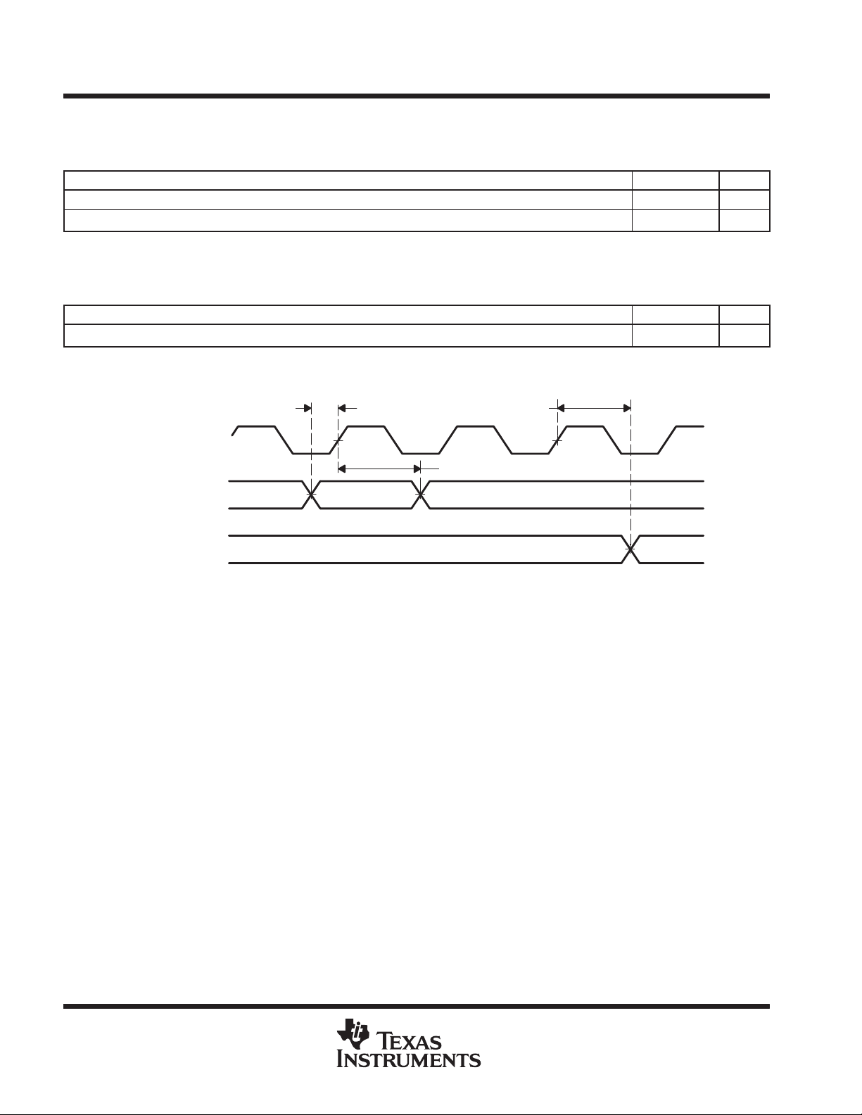
TMS320VC5420
FIXED-POINT DIGITAL SIGNAL PROCESSOR
SPRS080C – MARCH 1999 – REVISED APRIL 2000
multichannel buffered serial port timing (continued)
timing requirements for McBSP general-purpose I/O (see Figure 30)
t
su(BGPIO-COH)
t
h(COH-BGPIO)
†
BGPIOx refers to BCLKRx, BFSRx, BDRx, BCLKXx, or BFSXx when configured as a general-purpose input.
Setup time, BGPIOx input mode before CLKOUT high
Hold time, BGPIOx input mode after CLKOUT high
switching characteristics for McBSP general-purpose I/O (see Figure 30)
PARAMETER MIN MAX UNIT
t
d(COH-BGPIO)
‡
BGPIOx refers to BCLKRx, BFSRx, BCLKXx, BFSXx, or BDXx when configured as a general-purpose output.
Delay time, CLKOUT high to BGPIOx output mode
†
†
‡
MIN MAX UNIT
9 ns
0 ns
–10 10 ns
t
su(BGPIO-COH)
CLKOUT
BGPIOx Input
BGPIOx Output
†
BGPIOx refers to BCLKRx, BFSRx, BDRx, BCLKXx, or BFSXx when configured as a general-purpose input.
‡
BGPIOx refers to BCLKRx, BFSRx, BCLKXx, BFSXx, or BDXx when configured as a general-purpose output.
Mode
Mode
†
‡
t
d(COH-BGPIO)
t
h(COH-BGPIO)
Figure 30. McBSP General-Purpose I/O Timings
62
POST OFFICE BOX 1443 • HOUSTON, TEXAS 77251–1443
Page 63

FIXED-POINT DIGITAL SIGNAL PROCESSOR
multichannel buffered serial port timing (continued)
TMS320VC5420
SPRS080C – MARCH 1999 – REVISED APRIL 2000
timing requirements for McBSP as SPI master or slave: [H=0.5t
] CLKSTP = 10b, CLKXP = 0
c(CO)
(see Figure 31)
MASTER SLAVE
MIN MAX MIN MAX
t
su(BDRV-BCKXL)
t
h(BCKXL-BDRV)
t
su(BFXL-BCKXH)
t
c(BCKX)
†
For all SPI slave modes, CLKG is programmed as 1/2 of the CPU clock by setting CLKSM = CLKGDV = 1.
switching characteristics for McBSP as SPI master or slave: [H=0.5t
CLKXP = 0
t
h(BCKXL-BFXL)
t
d(BFXL-BCKXH)
t
d(BCKXH-BDXV)
t
dis(BCKXL-BDXHZ)
t
dis(BFXH-BDXHZ)
t
d(BFXL-BDXV)
†
For all SPI slave modes, CLKG is programmed as 1/2 of the CPU clock by setting CLKSM = CLKGDV = 1.
‡
T = BCLKX period = (1 + CLKGDV) * 2H
C = BCLKX low pulse width = T/2 when CLKGDV is odd or zero and = (CLKGDV/2) * 2H when CLKGDV is even
§
FSRP = FSXP = 1. As a SPI master, BFSX is inverted to provide active-low slave-enable output. As a slave, the active-low signal input on BFSX
and BFSR is inverted before being used internally.
CLKXM = FSXM = 1, CLKRM = FSRM = 0 for master McBSP
CLKXM = CLKRM = FSXM = FSRM = 0 for slave McBSP
¶
BFSX should be low before the rising edge of clock to enable slave devices and then begin a SPI transfer at the rising edge of the master clock
(BCLKX).
†
Setup time, BDR valid before BCLKX low 12 2 – 12H ns
Hold time, BDR valid after BCLKX low 4 6 + 12H ns
Setup time, BFSX low before BCLKX high 10 ns
Cycle time, BCLKX 12H 32H ns
] CLKSTP = 10b,
c(CO)
(see Figure 31)
PARAMETER
Hold time, BFSX low after BCLKX low
Delay time, BFSX low to BCLKX high
Delay time, BCLKX high to BDX valid –2 12 6H + 4 10H + 19 ns
Disable time, BDX high impedance following last data bit from BCLKX
low
Disable time, BDX high impedance following last data bit from BFSX
high
Delay time, BFSX low to BDX valid 4H + 4 8H + 17 ns
§
¶
MASTER
MIN MAX MIN MAX
T – 5 T + 5 ns
C – 5 C + 5 ns
C – 2 C +10 ns
‡
SLAVE
4H+ 4 8H + 17 ns
UNIT
UNIT
†
BCLKX
BFSX
BDX
BDR
t
LSB
t
h(BCKXL-BFXL)
t
Bit 0 Bit(n-1) (n-2) (n-3) (n-4)
Bit 0 Bit(n-1) (n-2) (n-3) (n-4)
t
su(BFXL-BCKXH)
t
dis(BFXH-BDXHZ)
dis(BCKXL-BDXHZ)
t
su(BDRV-BCLXL)
MSB
t
d(BFXL-BCKXH)
t
d(BFXL-BDXV)
t
d(BCKXH-BDXV)
t
h(BCKXL-BDRV)
c(BCKX)
Figure 31. McBSP Timing as SPI Master or Slave: CLKSTP = 10b, CLKXP = 0
POST OFFICE BOX 1443 • HOUSTON, TEXAS 77251–1443
63
Page 64
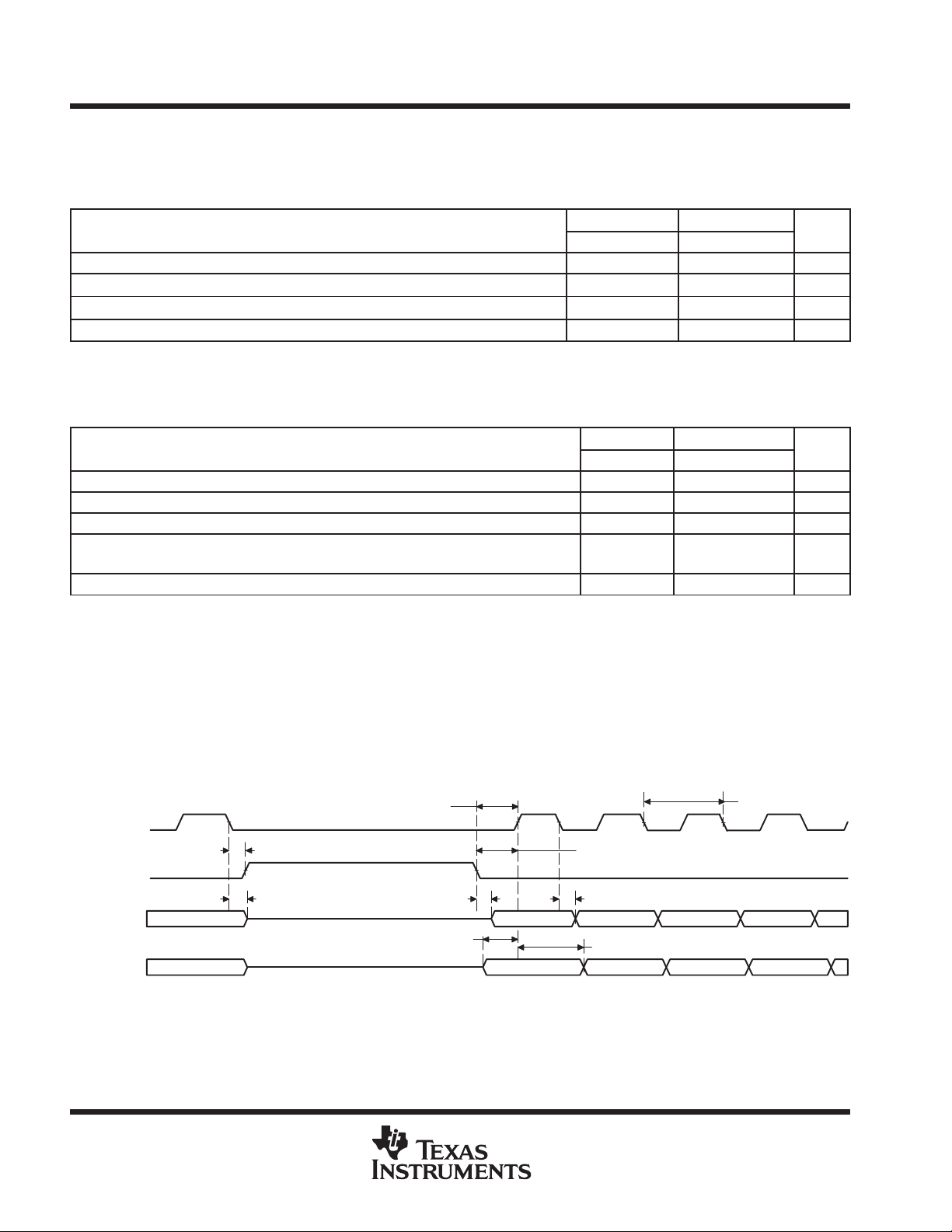
TMS320VC5420
FIXED-POINT DIGITAL SIGNAL PROCESSOR
SPRS080C – MARCH 1999 – REVISED APRIL 2000
multichannel buffered serial port timing (continued)
timing requirements for McBSP as SPI master or slave: [H=0.5t
] CLKSTP = 11b, CLKXP = 0
c(CO)
(see Figure 32)
MASTER SLAVE
MIN MAX MIN MAX
t
su(BDRV-BCKXH)
t
h(BCKXH-BDRV)
t
su(BFXL-BCKXH)
t
c(BCKX)
†
For all SPI slave modes, CLKG is programmed as 1/2 of the CPU clock by setting CLKSM = CLKGDV = 1.
switching characteristics for McBSP as SPI master or slave: [H=0.5t
CLKXP = 0
t
h(BCKXL-BFXL)
t
d(BFXL-BCKXH)
t
d(BCKXL-BDXV)
t
dis(BCKXL-BDXHZ)
t
d(BFXL-BDXV)
†
For all SPI slave modes, CLKG is programmed as 1/2 of the CPU clock by setting CLKSM = CLKGDV = 1.
‡
T = BCLKX period = (1 + CLKGDV) * 2H
C = BCLKX low pulse width = T/2 when CLKGDV is odd or zero and = (CLKGDV/2) * 2H when CLKGDV is even
D = BCLKX high pulse width = T/2 when CLKGDV is odd or zero and = (CLKGDV/2 + 1) * 2H when CLKGDV is even
§
FSRP = FSXP = 1. As a SPI master, BFSX is inverted to provide active-low slave-enable output. As a slave, the active-low signal input on BFSX
and BFSR is inverted before being used internally.
CLKXM = FSXM = 1, CLKRM = FSRM = 0 for master McBSP
CLKXM = CLKRM = FSXM = FSRM = 0 for slave McBSP
¶
BFSX should be low before the rising edge of clock to enable slave devices and then begin a SPI transfer at the rising edge of the master clock
(BCLKX).
Setup time, BDR valid before BCLKX high 12 2 – 12H ns
Hold time, BDR valid after BCLKX high 4 5 +12H ns
Setup time, BFSX low before BCLKX high 10 ns
Cycle time, BCLKX 12H 32H ns
] CLKSTP = 11b,
†
(see Figure 32)
PARAMETER
Hold time, BFSX low after BCLKX low
Delay time, BFSX low to BCLKX high
Delay time, BCLKX low to BDX valid –2 12 6H + 4 10H + 19 ns
Disable time, BDX high impedance following last data bit from BCLKX
low
Delay time, BFSX low to BDX valid D – 2 D +10 4H – 4 8H + 17 ns
§
¶
MASTER
MIN MAX MIN MAX
C – 5 C + 5 ns
T – 5 T + 5 ns
–2 10 6H + 4 10H + 17 ns
c(CO)
‡
SLAVE
UNIT
UNIT
†
BCLKX
BFSX
t
dis(BCKXL-BDXHZ)
BDX
BDR
64
t
LSB
t
h(BCKXL-BFXL)
Bit 0 Bit(n-1) (n-2) (n-3) (n-4)
Bit 0 Bit(n-1) (n-2) (n-3) (n-4)
t
su(BFXL-BCKXH)
t
d(BFXL-BDXV)
t
su(BDRV-BCKXH)
MSB
t
d(BFXL-BCKXH)
t
d(BCKXL-BDXV)
t
h(BCKXH-BDRV)
c(BCKX)
Figure 32. McBSP Timing as SPI Master or Slave: CLKSTP = 11b, CLKXP = 0
POST OFFICE BOX 1443 • HOUSTON, TEXAS 77251–1443
Page 65

FIXED-POINT DIGITAL SIGNAL PROCESSOR
multichannel buffered serial port timing (continued)
TMS320VC5420
SPRS080C – MARCH 1999 – REVISED APRIL 2000
timing requirements for McBSP as SPI master or slave: [H=0.5t
] CLKSTP = 10b, CLKXP = 1
c(CO)
(see Figure 33)
MASTER SLAVE
MIN MAX MIN MAX
t
su(BDRV-BCKXH)
t
h(BCKXH-BDRV)
t
su(BFXL-BCKXL)
t
c(BCKX)
†
For all SPI slave modes, CLKG is programmed as 1/2 of the CPU clock by setting CLKSM = CLKGDV = 1.
switching characteristics for McBSP as SPI master or slave: [H=0.5t
CLKXP = 1
t
h(BCKXH-BFXL)
t
d(BFXL-BCKXL)
t
d(BCKXL-BDXV)
t
dis(BCKXH-BDXHZ)
t
dis(BFXH-BDXHZ)
t
d(BFXL-BDXV)
†
For all SPI slave modes, CLKG is programmed as 1/2 of the CPU clock by setting CLKSM = CLKGDV = 1.
‡
T = BCLKX period = (1 + CLKGDV) * 2H
D = BCLKX high pulse width = T/2 when CLKGDV is odd or zero and = (CLKGDV/2 + 1) * 2H when CLKGDV is even
§
FSRP = FSXP = 1. As a SPI master, BFSX is inverted to provide active-low slave-enable output. As a slave, the active-low signal input on BFSX
and BFSR is inverted before being used internally.
CLKXM = FSXM = 1, CLKRM = FSRM = 0 for master McBSP
CLKXM = CLKRM = FSXM = FSRM = 0 for slave McBSP
¶
BFSX should be low before the rising edge of clock to enable slave devices and then begin a SPI transfer at the rising edge of the master clock
(BCLKX).
Setup time, BDR valid before BCLKX high 12 2 – 12H ns
Hold time, BDR valid after BCLKX high 4 6 + 12H ns
Setup time, BFSX low before BCLKX low 10 ns
Cycle time, BCLKX 12H 32H ns
] CLKSTP = 10b,
†‡
(see Figure 33)
Hold time, BFSX low after BCLKX high
Delay time, BFSX low to BCLKX low
Delay time, BCLKX low to BDX valid –2 12 6H + 4 10H + 19 ns
Disable time, BDX high impedance following last data bit from BCLKX
high
Disable time, BDX high impedance following last data bit from BFSX
high
Delay time, BFSX low to BDX valid 4H – 4 8H + 17 ns
PARAMETER
MASTER SLAVE
MIN MAX MIN MAX
§
¶
T – 5 T + 5 ns
D – 5 D + 5 ns
D – 2 D +10 ns
c(CO)
4H + 4 8H + 17 ns
UNIT
UNIT
†
BCLKX
BFSX
BDX
BDR
LSB
t
h(BCKXH-BFXL)
Bit 0 Bit(n-1) (n-2) (n-3) (n-4)
Bit 0 Bit(n-1) (n-2) (n-3) (n-4)
t
su(BFXL-BCKXL)
t
dis(BFXH-BDXHZ)
t
dis(BCKXH-BDXHZ)
t
su(BDRV-BCKXH)
MSB
t
d(BFXL-BCKXL)
t
d(BFXL-BDXV)
t
d(BCKXL-BDXV)
t
h(BCKXH-BDRV)
t
c(BCKX)
Figure 33. McBSP Timing as SPI Master or Slave: CLKSTP = 10b, CLKXP = 1
POST OFFICE BOX 1443 • HOUSTON, TEXAS 77251–1443
65
Page 66
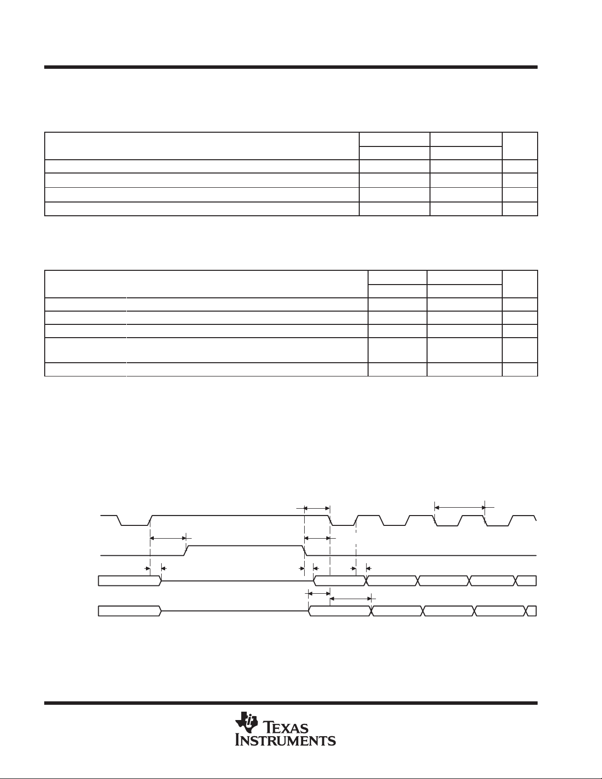
TMS320VC5420
FIXED-POINT DIGITAL SIGNAL PROCESSOR
SPRS080C – MARCH 1999 – REVISED APRIL 2000
multichannel buffered serial port timing (continued)
timing requirements for McBSP as SPI master or slave: [H=0.5t
] CLKSTP = 11b, CLKXP = 1
c(CO)
(see Figure 34)
MASTER SLAVE
MIN MAX MIN MAX
t
su(BDRV-BCKXL)
t
h(BCKXL-BDRV)
t
su(BFXL-BCKXL)
t
c(BCKX)
†
For all SPI slave modes, CLKG is programmed as 1/2 of the CPU clock by setting CLKSM = CLKGDV = 1.
switching characteristics for McBSP as SPI master or slave: [H=0.5t
CLKXP = 1
t
h(BCKXH-BFXL)
t
d(BFXL-BCKXL)
t
d(BCKXH-BDXV)
t
dis(BCKXH-BDXHZ)
t
d(BFXL-BDXV)
†
For all SPI slave modes, CLKG is programmed as 1/2 of the CPU clock by setting CLKSM = CLKGDV = 1.
‡
T = BCLKX period = (1 + CLKGDV) * 2H
C = BCLKX low pulse width = T/2 when CLKGDV is odd or zero and = (CLKGDV/2) * 2H when CLKGDV is even
D = BCLKX high pulse width = T/2 when CLKGDV is odd or zero and = (CLKGDV/2 + 1) * 2H when CLKGDV is even
§
FSRP = FSXP = 1. As a SPI master, BFSX is inverted to provide active-low slave-enable output. As a slave, the active-low signal input on BFSX
and BFSR is inverted before being used internally.
CLKXM = FSXM = 1, CLKRM = FSRM = 0 for master McBSP
CLKXM = CLKRM = FSXM = FSRM = 0 for slave McBSP
¶
BFSX should be low before the rising edge of clock to enable slave devices and then begin a SPI transfer at the rising edge of the master clock
(BCLKX).
Setup time, BDR valid before BCLKX low 12 2 – 12H ns
Hold time, BDR valid after BCLKX low 4 6 + 12H ns
Setup time, BFSX low before BCLKX low 10 ns
Cycle time, BCLKX 12H 32H ns
] CLKSTP = 11b,
†‡
(see Figure 34)
Hold time, BFSX low after BCLKX high
Delay time, BFSX low to BCLKX low
Delay time, BCLKX high to BDX valid –2 12 6H + 4 10H + 19 ns
Disable time, BDX high impedance following last data bit from BCLKX
high
Delay time, BFSX low to BDX valid C – 2 C +10 4H – 4 8H + 17 ns
PARAMETER
MASTER
MIN MAX MIN MAX
§
¶
D – 5 D + 5 ns
T – 5 T + 5 ns
–2 10 6H + 4 10H + 17 ns
c(CO)
‡
SLAVE
UNIT
UNIT
†
66
BCLKX
BFSX
t
dis(BCKXH-BDXHZ)
BDX
BDR
Figure 34. McBSP Timing as SPI Master or Slave: CLKSTP = 11b, CLKXP = 1
t
LSB
t
h(BCKXH-BFXL)
Bit 0 Bit(n-1) (n-2) (n-3) (n-4)
Bit 0 Bit(n-1) (n-2) (n-3) (n-4)
su(BFXL-BCKXL)
t
d(BFXL-BDXV)
t
su(BDRV-BCKXL)
POST OFFICE BOX 1443 • HOUSTON, TEXAS 77251–1443
MSB
t
d(BFXL-BCKXL)
t
d(BCKXH-BDXV)
t
h(BCKXL-BDRV)
t
c(BCKX)
Page 67
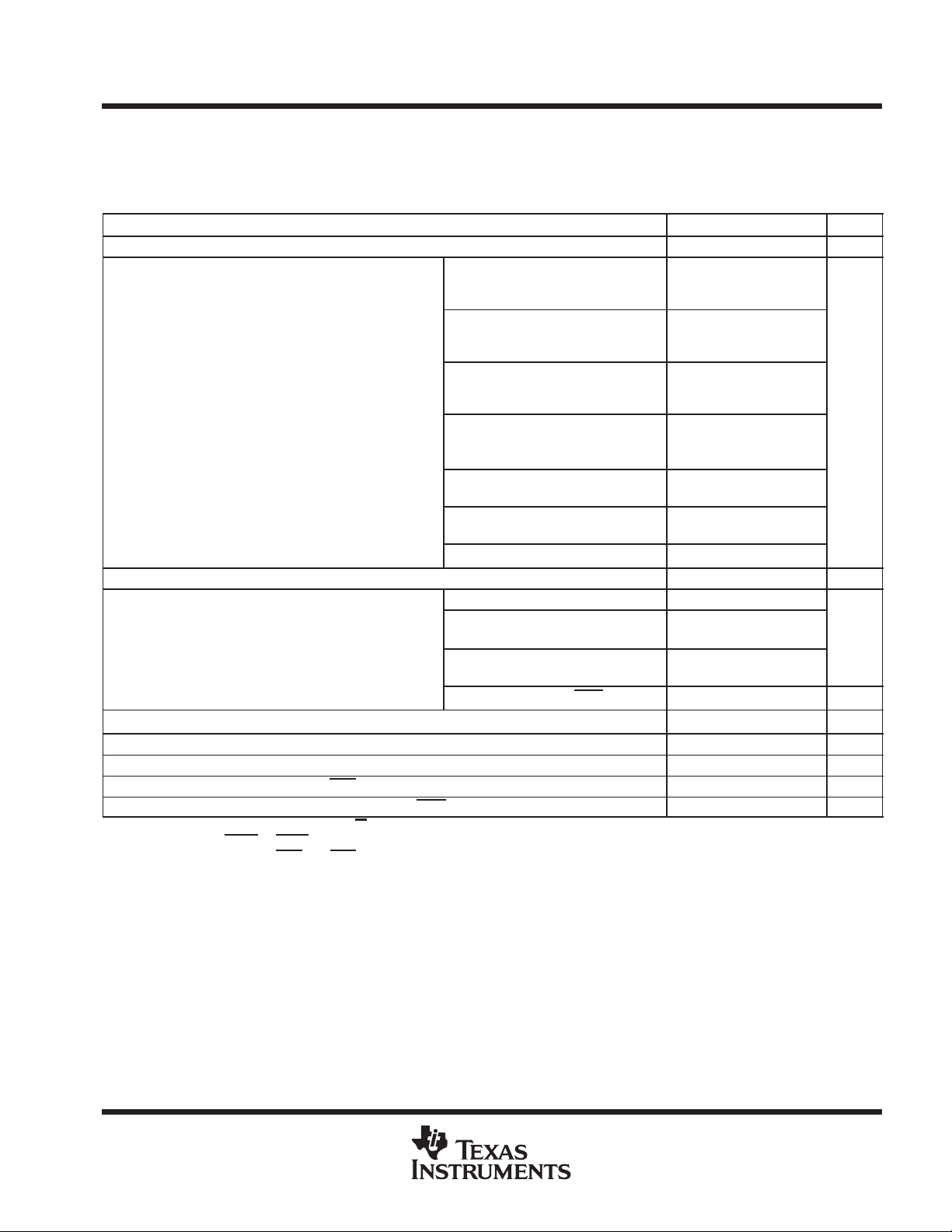
HPI16 timing
Delay time, DS low to HDx valid for first
Delay time, DS high to HRDY high
§
TMS320VC5420
FIXED-POINT DIGITAL SIGNAL PROCESSOR
SPRS080C – MARCH 1999 – REVISED APRIL 2000
switching characteristics over recommended operating conditions
(see Figure 35 – Figure 42)
PARAMETER MIN MAX UNIT
t
d(DSL-HDD)
t
d(DSL-HDV1)
t
d(DSL-HDV2)
t
d(DSH-HYH)
t
v(HYH-HDV)
t
h(DSH-HDV)R
t
d(COH-HYH)
t
d(DSH-HYL)
t
d(COH–HTX)
†
HAD stands for HCNTL0, HCNTL1, and HR/W.
‡
HDS refers to either HDS1
§
DS refers to the logical OR of HCS
Delay time, DS low to HD driven
Delay time, DS low to HDx valid for first
byte of an HPI read
Multiplexed reads with autoincrement. Prefetch completed. 3 20 ns
Delay time, DS high to HRDY high
(writes and autoincrement reads)
Valid time, HDx valid after HRDY high
Hold time, HD valid after DS rising edge, read
Delay time, CLKOUT rising edge to HRDY high 5 ns
Delay time, HDS or HCS high to HRDY low
Delay time, CLKOUT rising edge to HINT change 5 ns
or HDS2.
and HDS.
§
Case 1a: Memory accesses when
DMAC is active in 16-bit mode and
t
Case 1b: Memory accesses when
DMAC is active in 16-bit mode and
t
Case 1c: Memory access when
DMAC is active in 32-bit mode and
t
Case 1d: Memory access when
DMAC is active in 32-bit mode and
t
Case 2a: Memory accesses when
DMAC is inactive and t
Case 2b: Memory accesses when
DMAC is inactive and t
Case 3: Register accesses 20
No DMA channel active 12H+5
One or more 16-bit DMA channels
active
§
One or more 32-bit DMA channels
active
Writes to DSPINT and HINT 4H + 5
w(DSH)
w(DSH)
w(DSH)
w(DSH)
§
‡
< 18H
≥ 18H
< 26H
≥ 26H
w(DSH)
w(DSH)
< 10H
≥ 10H
†‡§
[H = 0.5t
3 20 ns
18H+20 – t
20
26H+20 – t
20
10H+20 – t
20
18H+5
26H+5
7 ns
0 10 ns
12 ns
c(CO)
w(DSH)
w(DSH)
ns
w(DSH)
ns
]
POST OFFICE BOX 1443 • HOUSTON, TEXAS 77251–1443
67
Page 68
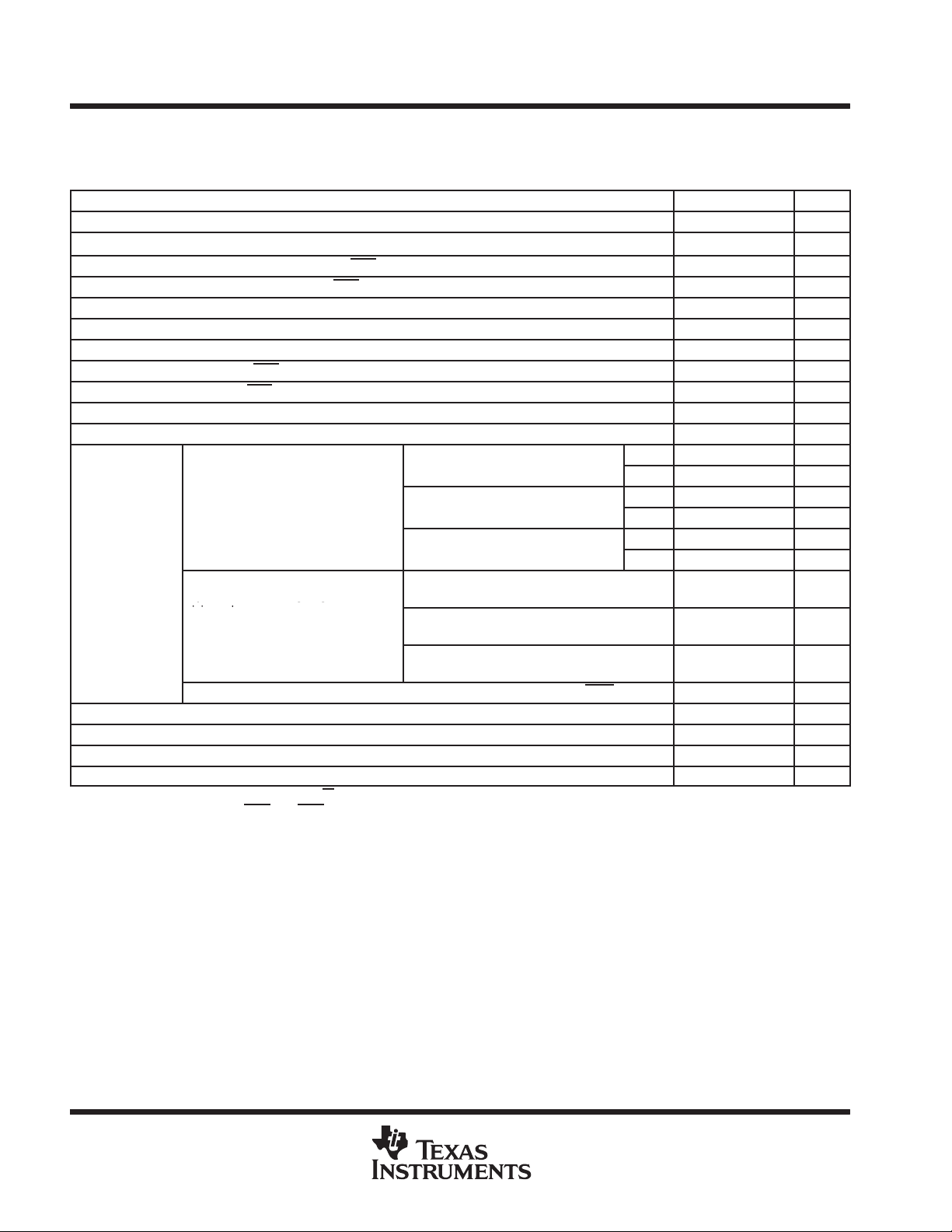
TMS320VC5420
Nonmulti lexed or multi lexed mode
Cycle time, DS rising edge to next DS
Nonmulti lexed or multi lexed mode
gg
Nonmulti lexed or multi lexed mode
ygg
(I
WRITE ti
FIXED-POINT DIGITAL SIGNAL PROCESSOR
SPRS080C – MARCH 1999 – REVISED APRIL 2000
HPI16 timing (continued)
timing requirements [H = 0.5t
t
su(HBV-DSL)
t
h(DSL-HBV)
t
su(HBV-HSL)
t
h(HSL-HBV)
t
su(HAV-DSH)
t
su(HAV-DSL)
t
h(DSH-HAV)
t
su(HSL-DSL)
t
h(HSL-DSL)
t
w(DSL)
t
w(DSH)
t
c(DSH-DSH)
t
su(HDV-DSH)
t
h(DSH-HDV)W
t
su(SELV-DSL)
t
h(DSH-SELV)
†
HAD stands for HCNTL0, HCNTL1, and HR/W.
‡
DS refers to the logical OR of HCS
Setup time, HAD valid before DS falling edge
Hold time, HAD valid after DS falling edge
Setup time, HAD valid before HAS falling edge
Hold time, HAD valid after HAS falling edge
Setup time, address valid before DS rising edge (nonmultiplexed write) 5 ns
Setup time, address valid before DS falling edge (nonmultiplexed mode)
Hold time, address valid after DS rising edge (nonmultiplexed mode)
Setup time, HAS low before DS falling edge
Hold time, HAS low after DS falling edge
Pulse duration, DS low
Pulse duration, DS high
Cycle time, DS rising edge to next DS Nonmultiplexed or multiplexed mode
rising edge
Cycle time, DS rising edge to next DS
rising edge
n autoincrement mode,
ings are the same as READ timings.)
Cycle time, DS rising edge to next DS rising edge writes to DSPINT and HINT 8H ns
Setup time, HD valid before DS rising edge
Hold time, HD valid after DS rising edge, write
Setup time, SELA/B valid before DS falling edge
Hold time, SELA/B valid after DS Rising edge
‡
‡
and HDS.
] (see Note 1 and Figure 35 – Figure 42)
c(CO)
†‡
†‡
†
†
‡
‡
‡
‡
‡
Nonmultiplexed or multiplexed mode
(no increment) with no DMA activity.
(no increment) with 16-bit DMA activity.
Nonmultiplexed or multiplexed mode
(no increment) with 32-bit DMA activity.
Multiplexed (autoincrement) with no DMA
activity.
Multiplexed (autoincrement) with 16-bit DMA
activity.
-
m-
Multiplexed (autoincrement) with 32-bit DMA
activity.
‡
‡
‡
‡
MIN MAX UNIT
5 ns
5 ns
5 ns
5 ns
‡
Reads 12H ns
Writes 14H ns
Reads 18H ns
Writes 20H
Reads 26H ns
Writes 28H
–4H – 5 ns
1 ns
5 ns
2 ns
30 ns
10 ns
12H ns
18H ns
26H ns
10 ns
0 ns
5 ns
0 ns
68
POST OFFICE BOX 1443 • HOUSTON, TEXAS 77251–1443
Page 69
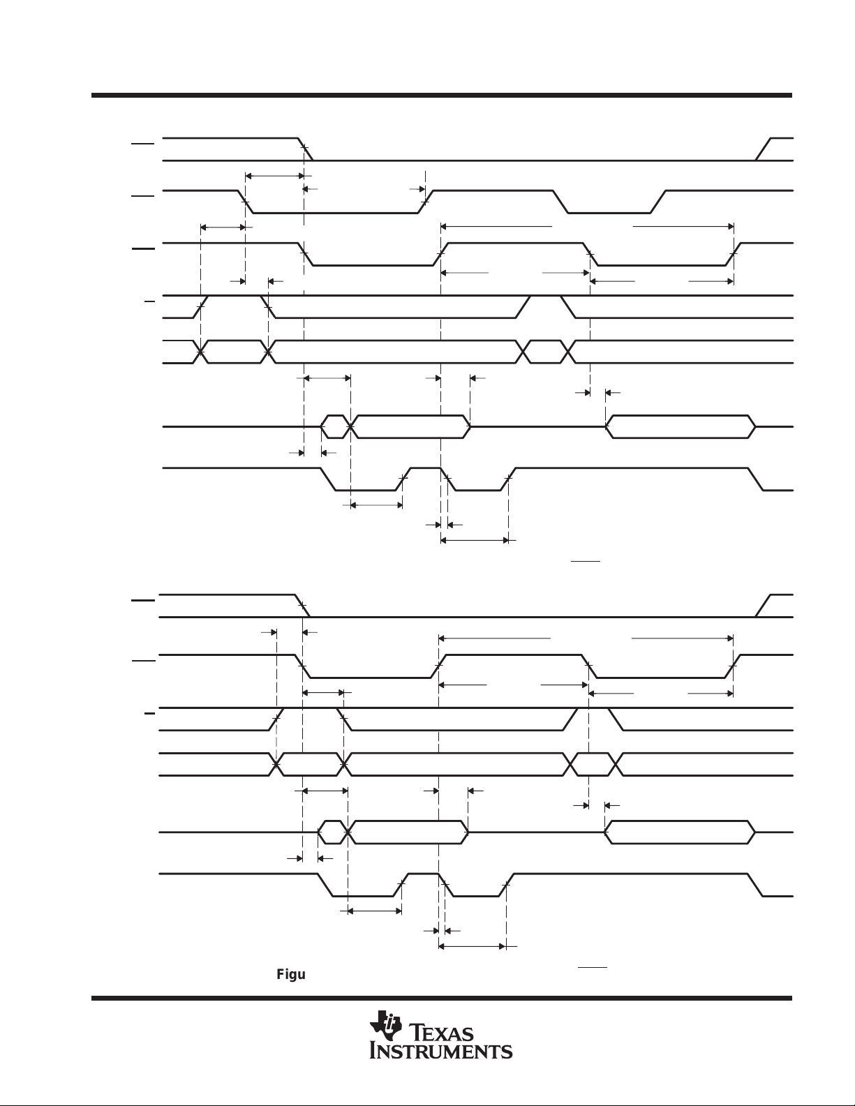
HPI16 timing (continued)
HCS
HAS
t
su(HSL–DSL)
t
h(HSL–DSL)
TMS320VC5420
FIXED-POINT DIGITAL SIGNAL PROCESSOR
SPRS080C – MARCH 1999 – REVISED APRIL 2000
HDS
HR/W
HCNTL[1:0]
HD[15:0]
HRDY
HCS
t
su(HBV–HSL)
t
d(DSL–HDV1)
t
d(DSL–HDD)
t
t
t
h(HSL–HBV)
v(HYH–HDV)
t
d(DSH–HYL)
w(DSH)
0101
t
h(DSH–HDV)R
t
d(DSH–HYH)
Figure 35. Multiplexed Read Timings Using HAS
t
c(DSH–DSH)
t
w(DSL)
t
d(DSL–HDV2)
PF DataData 1
HDS
HR/W
HCNTL[1:0]
HD[15:0]
HRDY
t
su(HBV–DSL)
t
d(DSL–HDV1)
t
d(DSL–HDD)
t
w(DSH)
t
h(DSH–HDV)R
t
d(DSH–HYH)
t
v(HYH–HDV)
t
h(DSL–HBV)
t
d(DSH–HYL)
Figure 36. Multiplexed Read Timings Without HAS
t
c(DSH–DSH)
0101
t
w(DSL)
t
d(DSL–HDV2)
PF DataData 1
POST OFFICE BOX 1443 • HOUSTON, TEXAS 77251–1443
69
Page 70
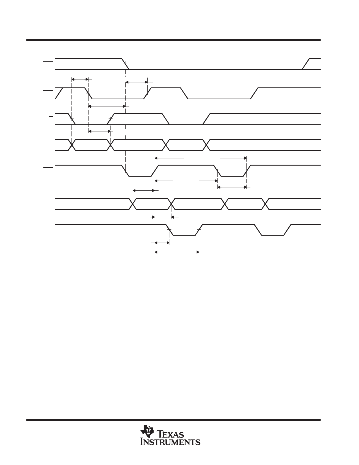
TMS320VC5420
FIXED-POINT DIGITAL SIGNAL PROCESSOR
SPRS080C – MARCH 1999 – REVISED APRIL 2000
HPI16 timing (continued)
HCS
t
HAS
HR/W
su(HBV–HSL)
t
h(HSL–HBV)
t
su(HSL–DSL)
t
h(HSL–DSL)
HCNTL[0:1]
HDS
HRDY
0101
t
c(DSH–DSH)
t
w(DSH)
t
su(HDV–DSH)
t
h(DSH–HDV)W
t
d(DSH–HYL)
t
d(DSH–HYH)
Figure 37. Multiplexed Write Timings Using HAS
t
w(DSL)
Data nData 1HD[15:0]
70
POST OFFICE BOX 1443 • HOUSTON, TEXAS 77251–1443
Page 71

HPI16 timing (continued)
HCS
HDS
TMS320VC5420
FIXED-POINT DIGITAL SIGNAL PROCESSOR
SPRS080C – MARCH 1999 – REVISED APRIL 2000
t
t
w(DSH)
c(DSH–DSH)
HR/W
HCNTL[1:0]
HD[15:0]
HRDY
t
su(HBV–DSL
t
su(HDV–DSH)
)
t
h(DSL–HBV)
0101
t
h(DSH–HDV)W
t
d(DSH–HYL)
t
d(DSH–HYH)
Figure 38. Multiplexed Write Timings Without HAS
t
w(DSL)
Data nData 1
POST OFFICE BOX 1443 • HOUSTON, TEXAS 77251–1443
71
Page 72
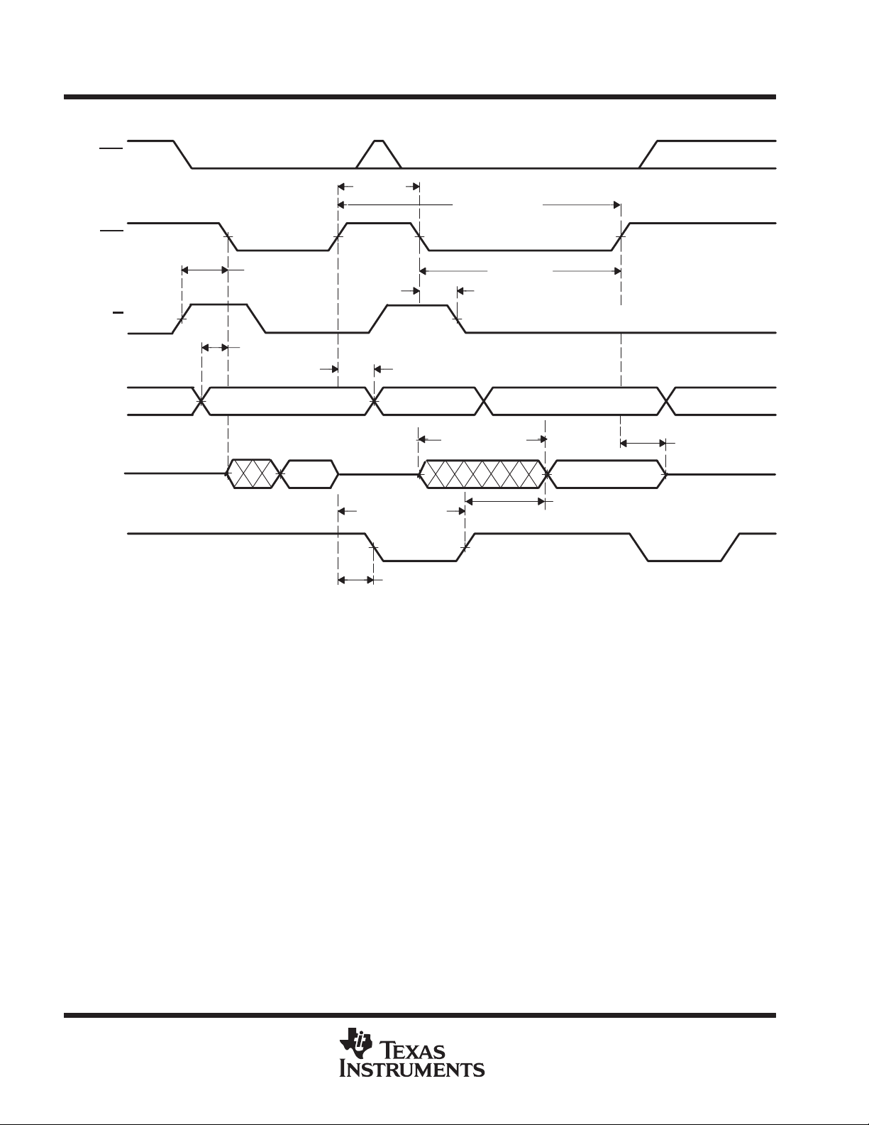
TMS320VC5420
FIXED-POINT DIGITAL SIGNAL PROCESSOR
SPRS080C – MARCH 1999 – REVISED APRIL 2000
HPI16 timing (continued)
HCS
t
w(DSH)
HDS
t
c(DSH–DSH)
HR/W
HA[17:0]
HD[15:0]
HRDY
t
su(HBV–DSL)
t
su(HAV–DSL)
t
h(DSH–HAV)
t
d(DSL–HDV1)
Data
t
d(DSH–HYH)
t
d(DSH–HYL)
Figure 39. Nonmultiplexed Read Timings
t
w(DSL)
t
h(DSL–HBV)
Valid AddressValid Address
t
v(HYH–HDV)
Data Valid
t
h(DSH–HDV)R
72
POST OFFICE BOX 1443 • HOUSTON, TEXAS 77251–1443
Page 73

HPI16 timing (continued)
HCS
HDS
t
w(DSH)
TMS320VC5420
FIXED-POINT DIGITAL SIGNAL PROCESSOR
SPRS080C – MARCH 1999 – REVISED APRIL 2000
t
c(DSH–DSH)
HR/W
HA[17:0]
HD[15:0]
HRDY
t
su(HBV–DSL)
t
su(HAV–DSH)
t
h(DSH–HAV)
t
su(HDV–DSH)
t
d(DSH–HYH)
t
d(DSH–HYL)
Figure 40. Nonmultiplexed Write Timings
t
w(DSL)
t
h(DSL–HBV)
Valid AddressValid Address
t
h(DSH–HDV)W
Data ValidData Valid
POST OFFICE BOX 1443 • HOUSTON, TEXAS 77251–1443
73
Page 74
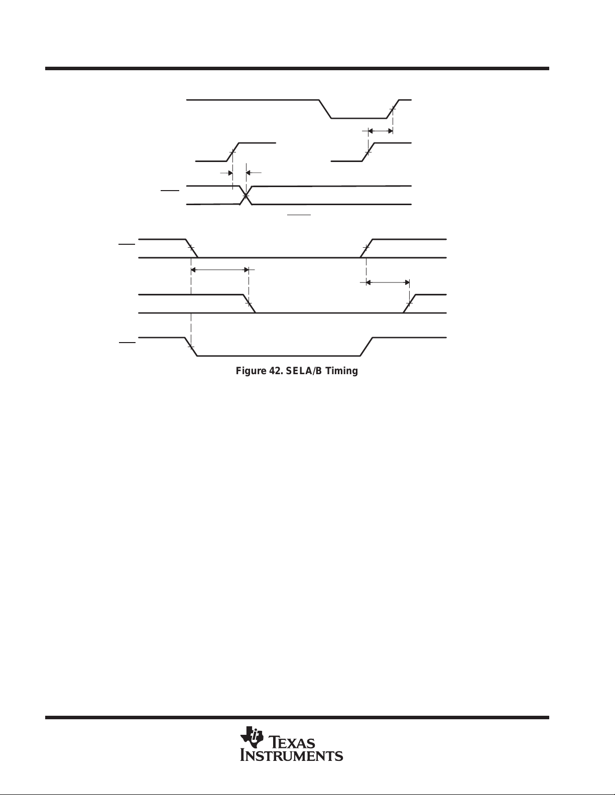
TMS320VC5420
FIXED-POINT DIGITAL SIGNAL PROCESSOR
SPRS080C – MARCH 1999 – REVISED APRIL 2000
HPI16 timing (continued)
HRDY
CLKOUT
t
d(COH–HTX)
HINT
Figure 41. HRDY and HINT Relative to CLKOUT
HCS
t
su(DSL–SELV)
SELA/B
t
d(COH–HYH)
t
h(DSH–SELV)
HDS
Figure 42. SELA/B Timing
74
POST OFFICE BOX 1443 • HOUSTON, TEXAS 77251–1443
Page 75
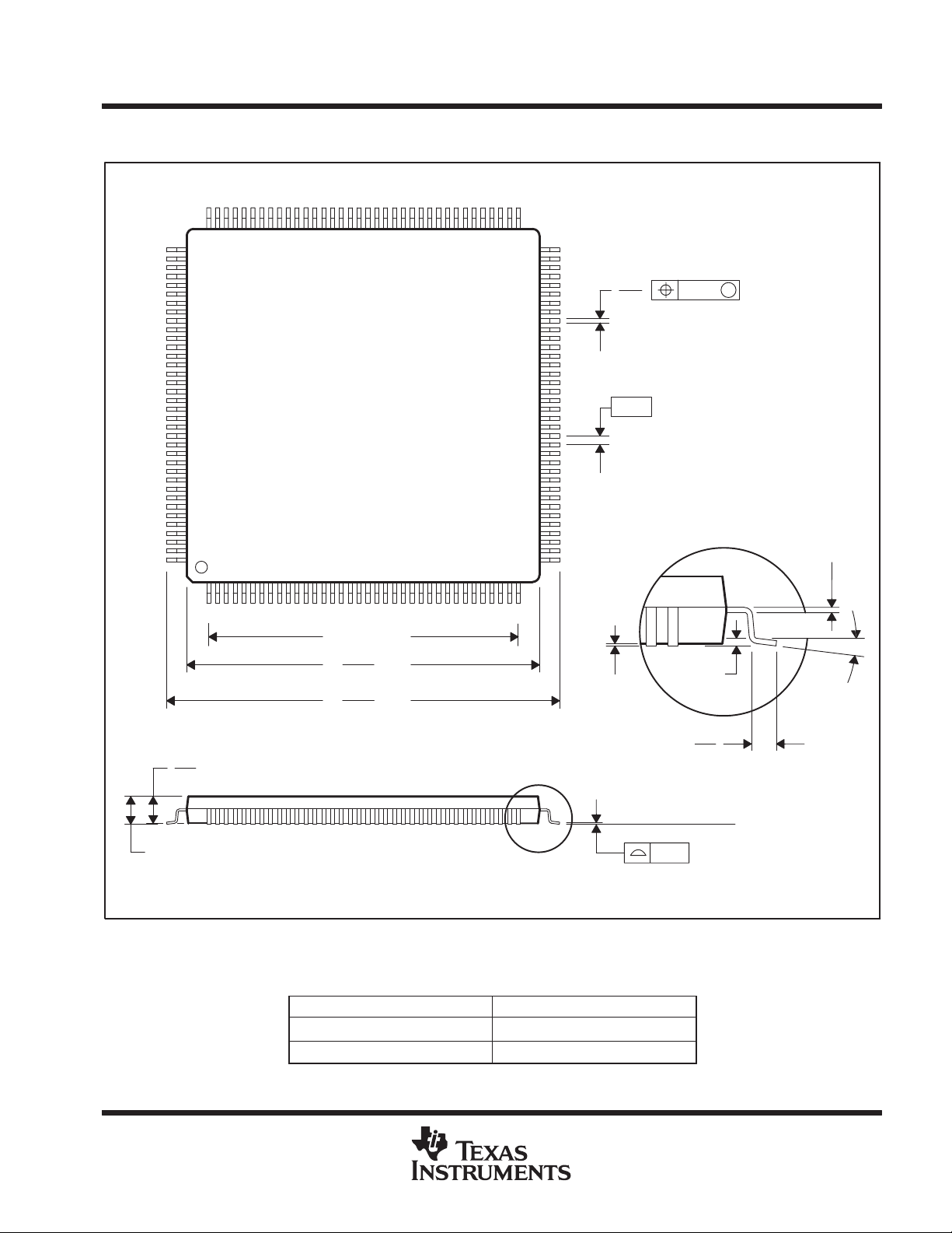
TMS320VC5420
FIXED-POINT DIGITAL SIGNAL PROCESSOR
SPRS080C – MARCH 1999 – REVISED APRIL 2000
MECHANICAL DATA
PGE (S-PQFP-G144) PLASTIC QUAD FLATPACK
109
144
1,45
1,35
108
73
72
0,27
0,17
0,50
37
1
17,50 TYP
20,20
SQ
19,80
22,20
SQ
21,80
36
0,05 MIN
0,08
0,25
0,75
0,45
M
0,13 NOM
Gage Plane
0°–7°
1,60 MAX
NOTES: A. All linear dimensions are in millimeters.
B. This drawing is subject to change without notice.
C. Falls within JEDEC MS-026
PARAMETER
R
ΘJA
R
ΘJC
POST OFFICE BOX 1443 • HOUSTON, TEXAS 77251–1443
Seating Plane
0,08
4040147/C 10/96
Thermal Resistance Characteristics
°C/W
56
5
75
Page 76

TMS320VC5420
FIXED-POINT DIGITAL SIGNAL PROCESSOR
SPRS080C – MARCH 1999 – REVISED APRIL 2000
MECHANICAL DATA
GGU (S-PBGA-N144) PLASTIC BALL GRID ARRAY
0,95
0,85
0,12
0,08
0,55
0,45
12,10
11,90
SQ
0,08
9,60 TYP
0,80
N
M
L
K
J
H
G
F
E
D
C
B
A
1
1,40 MAX
Seating Plane
M
0,45
0,35
0,10
42 3
5
12 1310 118967
4073221/A 11/96
0,80
NOTES: A. All linear dimensions are in millimeters.
MicroStar BGA is a trademark of Texas Instruments Incorporated.
B. This drawing is subject to change without notice.
C. MicroStar BGA configuration
Thermal Resistance Characteristics
PARAMETER
R
ΘJA
R
ΘJC
°C/W
38
5
76
POST OFFICE BOX 1443 • HOUSTON, TEXAS 77251–1443
Page 77

IMPORTANT NOTICE
T exas Instruments and its subsidiaries (TI) reserve the right to make changes to their products or to discontinue
any product or service without notice, and advise customers to obtain the latest version of relevant information
to verify, before placing orders, that information being relied on is current and complete. All products are sold
subject to the terms and conditions of sale supplied at the time of order acknowledgment, including those
pertaining to warranty, patent infringement, and limitation of liability.
TI warrants performance of its semiconductor products to the specifications applicable at the time of sale in
accordance with TI’s standard warranty. Testing and other quality control techniques are utilized to the extent
TI deems necessary to support this warranty . Specific testing of all parameters of each device is not necessarily
performed, except those mandated by government requirements.
Customers are responsible for their applications using TI components.
In order to minimize risks associated with the customer’s applications, adequate design and operating
safeguards must be provided by the customer to minimize inherent or procedural hazards.
TI assumes no liability for applications assistance or customer product design. TI does not warrant or represent
that any license, either express or implied, is granted under any patent right, copyright, mask work right, or other
intellectual property right of TI covering or relating to any combination, machine, or process in which such
semiconductor products or services might be or are used. TI’s publication of information regarding any third
party’s products or services does not constitute TI’s approval, warranty or endorsement thereof.
Copyright 2000, Texas Instruments Incorporated
 Loading...