

Texas Instruments TMX320VC5409PGE100, TMX320VC5409GGU100, TMS320VC5409GGU100, TMS320VC5409GGU-80, TMS320VC5409PGE100 Datasheet
...
TMS320VC5409
FIXED-POINT DIGITAL SIGNAL PROCESSOR
SPRS082C – APRIL 1999 – REVISED MARCH 2000
1
POST OFFICE BOX 1443 • HOUSTON, TEXAS 77251–1443
Advanced Multibus Architecture With Three
Separate 16-Bit Data Memory Buses and
One Program Memory Bus
40-Bit Arithmetic Logic Unit (ALU),
Including a 40-Bit Barrel Shifter and Two
Independent 40-Bit Accumulators
17- × 17-Bit Parallel Multiplier Coupled to a
40-Bit Dedicated Adder for Non-Pipelined
Single-Cycle Multiply/Accumulate (MAC)
Operation
Compare, Select, and Store Unit (CSSU) for
the Add/Compare Selection of the Viterbi
Operator
Exponent Encoder to Compute an
Exponent Value of a 40-Bit Accumulator
Value in a Single Cycle
T wo Address Generators With Eight
Auxiliary Registers and Two Auxiliary
Register Arithmetic Units (ARAUs)
Data Bus With a Bus-Holder Feature
Extended Addressing Mode for 8M × 16-Bit
Maximum Addressable External Program
Space
16K x 16-Bit On-Chip ROM
32K x 16-Bit Dual-Access On-Chip RAM
Single-Instruction-Repeat and
Block-Repeat Operations for Program Code
Block-Memory-Move Instructions for Better
Program and Data Management
Instructions With a 32-Bit Long Word
Operand
Instructions With Two- or Three-Operand
Reads
Arithmetic Instructions With Parallel Store
and Parallel Load
Conditional Store Instructions
Fast Return From Interrupt
On-Chip Peripherals
– Software-Programmable Wait-State
Generator and Programmable Bank
Switching
– On-Chip Phase-Locked Loop (PLL) Clock
Generator With Internal Oscillator or
External Clock Source
– Three Multichannel Buffered Serial Ports
(McBSPs)
– Enhanced 8-Bit Parallel Host-Port
Interface With 16-Bit Data/Addressing
– One 16-Bit Timer
– Six-Channel Direct Memory Access
(DMA) Controller
Power Consumption Control With IDLE1,
IDLE2, and IDLE3 Instructions With
Power-Down Modes
CLKOUT Off Control to Disable CLKOUT
On-Chip Scan-Based Emulation Logic,
IEEE Std 1149.1† (JTAG) Boundary Scan
Logic
12.5-ns Single-Cycle Fixed-Point
Instruction Execution Time (80 MIPS) for
3.3-V Power Supply (1.8-V Core)
10-ns Single-Cycle Fixed-Point Instruction
Execution Time (100 MIPS) for 3.3-V Power
Supply (1.8-V Core)
Available in a 144-Pin Plastic Thin Quad
Flatpack (TQFP) (PGE Suffix) and a 144-Pin
Ball Grid Array (BGA) (GGU Suffix)
NOTE:This data sheet is designed to be used in conjunction with the
TMS320C5000 DSP Family Functional Overview
(literature number SPRU307).
Please be aware that an important notice concerning availability, standard warranty, and use in critical applications of
Texas Instruments semiconductor products and disclaimers thereto appears at the end of this data sheet.
Copyright 2000, Texas Instruments Incorporated
†
IEEE Standard 1149.1-1990 Standard-Test-Access Port and Boundary Scan Architecture.
PRODUCTION DATA information is current as of publication date.
Products conform to specifications per the terms of Texas Instruments
standard warranty. Production processing does not necessarily include
testing of all parameters.

TMS320VC5409
FIXED-POINT DIGITAL SIGNAL PROCESSOR
SPRS082C – APRIL 1999 – REVISED MARCH 2000
2
POST OFFICE BOX 1443 • HOUSTON, TEXAS 77251–1443
Table of Contents
Internal Oscillator with External Crystal 40. . . . . . . .
Divide-by-Two/Divide-by-Four Clock Option 41. . . .
Multiply-by-N Clock Option 42. . . . . . . . . . . . . . . . . . .
Memory and Parallel I/O Interface Timing 43. . . . . .
Timing For Externally Generated Wait States 49. . .
HOLD
and HOLDA Timings 53. . . . . . . . . . . . . . . . . .
Reset, BIO
, Interrupt, and MP/MC Timings 55. . . . .
Instruction Acquisition (IAQ
), Interrupt
Acknowledge (IACK
), External Flag (XF),
and TOUT Timings 57. . . . . . . . . . . . . . . . . . . . .
Multichannel Buffered Serial Port Timing 59. . . . . . .
HPI8 Timing 67. . . . . . . . . . . . . . . . . . . . . . . . . . . . . . .
HPI16 Timing 72. . . . . . . . . . . . . . . . . . . . . . . . . . . . . .
Mechanical Data 76. . . . . . . . . . . . . . . . . . . . . . . . . . .
Description 2. . . . . . . . . . . . . . . . . . . . . . . . . . . . . . . . . . .
Pin Assignments 5. . . . . . . . . . . . . . . . . . . . . . . . . . . . . .
Terminal Functions 6. . . . . . . . . . . . . . . . . . . . . . . . . . .
Memory 1 1. . . . . . . . . . . . . . . . . . . . . . . . . . . . . . . . . . . . .
On-chip Peripherals 15. . . . . . . . . . . . . . . . . . . . . . . . . .
Memory-mapped Registers 30. . . . . . . . . . . . . . . . . . . .
McBSP Control Registers And Subaddresses 33. . . .
DMA Subbank Addressed Registers 33. . . . . . . . . . . .
Interrupts 35. . . . . . . . . . . . . . . . . . . . . . . . . . . . . . . . . . . .
Documentation Support 37. . . . . . . . . . . . . . . . . . . . . . .
Absolute Maximum Ratings 38. . . . . . . . . . . . . . . . . . .
Recommended Operating Conditions 38. . . . . . . . . . .
Electrical Characteristics 39. . . . . . . . . . . . . . . . . . . . . .
Parameter Measurement Information 39. . . . . . . . . . . .
description
The TMS320VC5409 fixed-point, digital signal processor (DSP) (hereafter referred to as the ’5409 unless
otherwise specified) is based on an advanced modified Harvard architecture that has one program memory bus
and three data memory buses. This processor provides an arithmetic logic unit (ALU) with a high degree of
parallelism, application-specific hardware logic, on-chip memory , and additional on-chip peripherals. The basis
of the operational flexibility and speed of this DSP is a highly specialized instruction set.
Separate program and data spaces allow simultaneous access to program instructions and data, providing the
high degree of parallelism. Two read operations and one write operation can be performed in a single cycle.
Instructions with parallel store and application-specific instructions can fully utilize this architecture. In addition,
data can be transferred between data and program spaces. Such parallelism supports a powerful set of
arithmetic, logic, and bit-manipulation operations that can all be performed in a single machine cycle. In addition,
the ’5409 includes the control mechanisms to manage interrupts, repeated operations, and function calls.

TMS320VC5409
FIXED-POINT DIGITAL SIGNAL PROCESSOR
SPRS082C – APRIL 1999 – REVISED MARCH 2000
3
POST OFFICE BOX 1443 • HOUSTON, TEXAS 77251–1443
CV
HDS1
A18
A17
V
SS
A16
D5
D4
D3
D2
D1
D0
RS
X2/CLKIN
X1
HD3
CLKOUT
V
SS
HPIENA
CV
DD
V
SS
TMS
TCK
TRST
TDI
TDO
EMU1/OFF
EMU0
TOUT
HD2
HPI16
CLKMD3
CLKMD2
CLKMD1
V
SS
DV
DD
BDX1
BFSX1
V
SS
A22
V
SS
DV
DD
A10
HD7
A11
A12
A13
A14
A15
CV
DD
HAS
V
SS
V
SS
CV
DD
HCS
HR/W
READY
PS
DS
IS
R/W
MSTRB
IOSTRB
MSC
XF
HOLDA
IAQ
HOLD
BIO
MP/MC
DV
DD
V
SS
BDR1
BFSR1
144
A21
CV
143
142
141A8140A7139A6138A5137A4136
HD6
135A3134A2133A1132A0131DV130
129
128
127
126
125
HD5
124
D15
123
D14
122
D13
121
HD4
120
D12
119
D11
118
117D9116D8115D7114D6113
112
373839404142434445464748495051525354555657585960616263646566676869
1
2
3
4
5
6
7
8
9
10
11
12
13
14
15
16
17
18
19
20
21
22
23
24
25
26
27
28
29
30
31
32
33
34
35
36
108
107
106
105
104
103
102
101
100
99
98
97
96
95
94
93
92
91
90
89
88
87
86
85
84
83
82
81
80
79
78
77
76
75
74
73
BCLKR1
HCNTL0SSBCLKR0
BCLKR2
BFSR0
BFSR2
BDR0
HCNTL1
BDR2
BCLKX0
BCLKX2
SS
DD
SS
HD0
BDX0
BDX2
IACK
HBIL
NMI
INT0
INT1
INT2
INT3
DD
HD1
SS
HRDY
HINT
111
V
110
A19
109
707172
BCLKX1
D10
A20
DV
DD
CV
HDS2SSV
V
V
DV
V
CV
V
DD
DD
DD
DD
SS
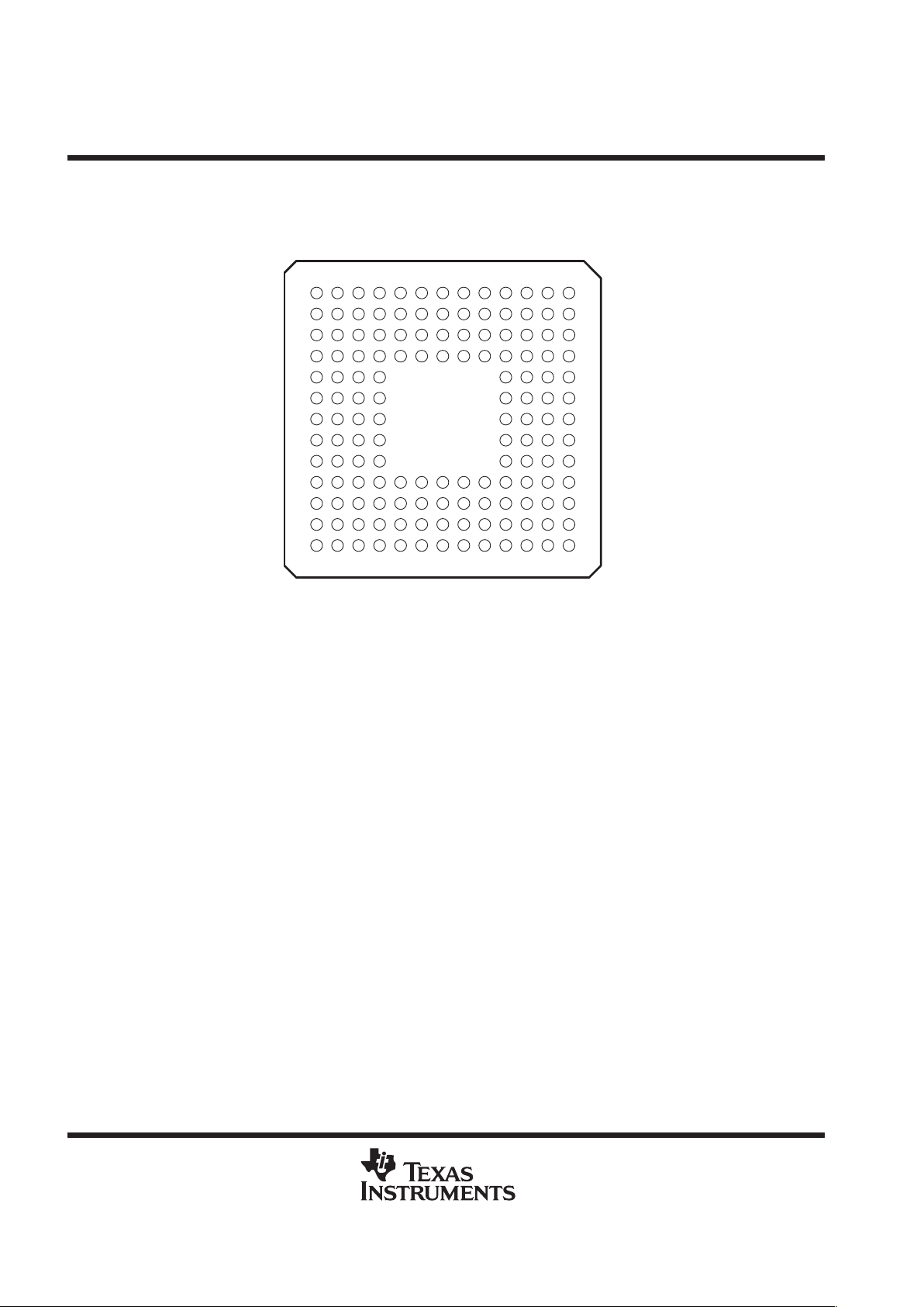
TMS320VC5409 PGE PACKAGE
†‡
(TOP VIEW)
BFSX0
A9
BFSX2
SS
V
V
SS
SS
V
SS
V
NOTE: DVDD is the power supply for the I/O pins while CVDD is the power supply for the core CPU. VSS is the ground for both the I/O pins and
the core CPU.
The TMS320VC5409PGE (144-pin TQFP) package is footprint-compatible with the ’LC548, ’LC/VC549, and
’VC5410 devices.
TMS320VC5409
FIXED-POINT DIGITAL SIGNAL PROCESSOR
SPRS082C – APRIL 1999 – REVISED MARCH 2000
4
POST OFFICE BOX 1443 • HOUSTON, TEXAS 77251–1443
TMS320VC5409 GGU PACKAGE
(BOTTOM VIEW)
A
B
D
C
E
F
H
J
L
M
K
N
G
12
3456781012 1113 9
The pin assignments table to follow lists each signal quadrant and BGA ball number for the
TMS320VC5409GGU (144-pin BGA package) which is footprint-compatible with the ’LC548, ’LC/VC549, and
’VC5410 devices.
TMS320VC5409
FIXED-POINT DIGITAL SIGNAL PROCESSOR
SPRS082C – APRIL 1999 – REVISED MARCH 2000
5
POST OFFICE BOX 1443 • HOUSTON, TEXAS 77251–1443
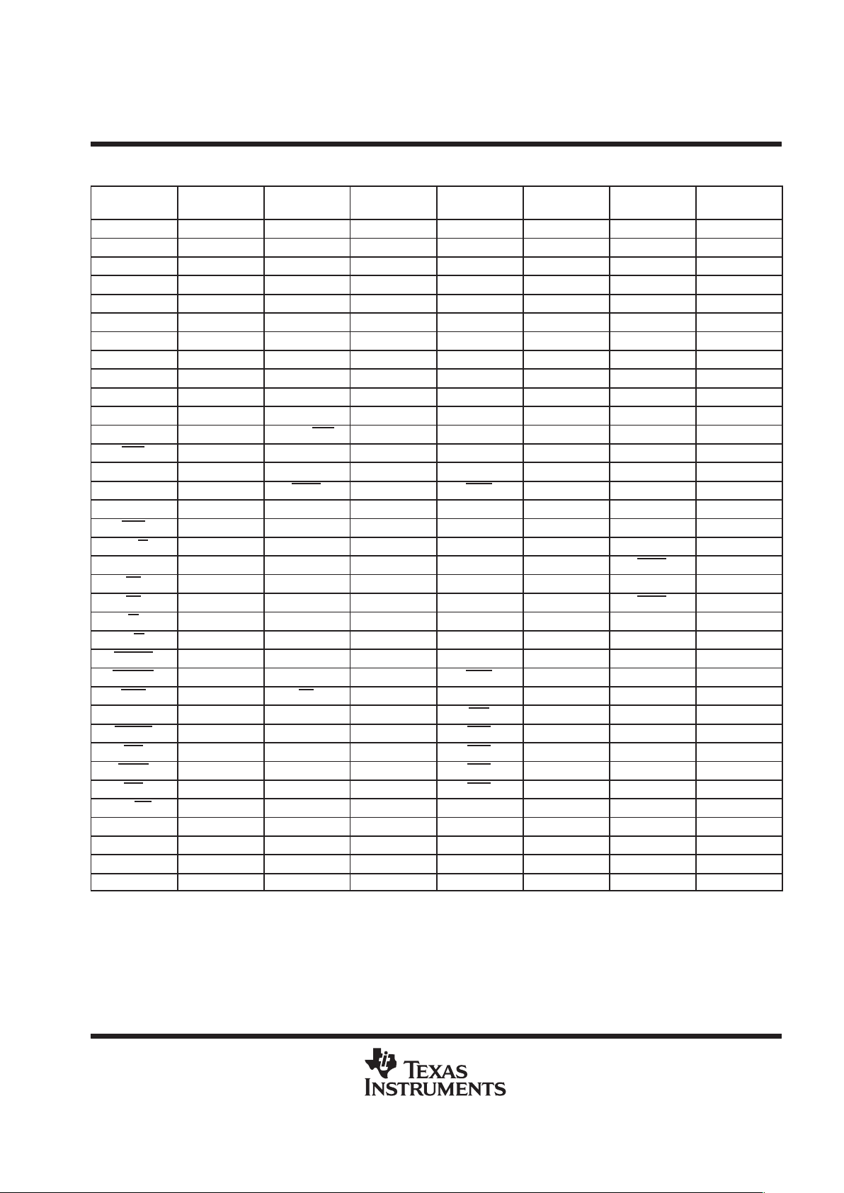
Pin Assignments for the TMS320VC5409GGU (144-Pin BGA Package)
†
SIGNAL
QUADRANT 1
BGA BALL #
SIGNAL
QUADRANT 2
BGA BALL #
SIGNAL
QUADRANT 3
BGA BALL #
SIGNAL
QUADRANT 4
BGA BALL #
V
SS
A1 BFSX1 N13 V
SS
N1 A19 A13
A22 B1 BDX1 M13 BCLKR1 N2 A20 A12
V
SS
C2 DV
DD
L12 HCNTL0 M3 V
SS
B11
DV
DD
C1 V
SS
L13 V
SS
N3 DV
DD
A11
A10 D4 CLKMD1 K10 BCLKR0 K4 D6 D10
HD7 D3 CLKMD2 K11 BCLKR2 L4 D7 C10
A11 D2 CLKMD3 K12 BFSR0 M4 D8 B10
A12 D1 HPI16 K13 BFSR2 N4 D9 A10
A13 E4 HD2 J10 BDR0 K5 D10 D9
A14 E3 TOUT J11 HCNTL1 L5 D11 C9
A15 E2 EMU0 J12 BDR2 M5 D12 B9
CV
DD
E1 EMU1/OFF J13 BCLKX0 N5 HD4 A9
HAS F4 TDO H10 BCLKX2 K6 D13 D8
V
SS
F3 TDI H11 V
SS
L6 D14 C8
V
SS
F2 TRST H12 HINT M6 D15 B8
CV
DD
F1 TCK H13 CV
DD
N6 HD5 A8
HCS G2 TMS G12 BFSX0 M7 CV
DD
B7
HR/W G1 V
SS
G13 BFSX2 N7 V
SS
A7
READY G3 CV
DD
G11 HRDY L7 HDS1 C7
PS G4 HPIENA G10 DV
DD
K7 V
SS
D7
DS H1 V
SS
F13 V
SS
N8 HDS2 A6
IS H2 CLKOUT F12 HD0 M8 DV
DD
B6
R/W H3 HD3 F11 BDX0 L8 A0 C6
MSTRB H4 X1 F10 BDX2 K8 A1 D6
IOSTRB J1 X2/CLKIN E13 IACK N9 A2 A5
MSC J2 RS E12 HBIL M9 A3 B5
XF J3 D0 E11 NMI L9 HD6 C5
HOLDA J4 D1 E10 INT0 K9 A4 D5
IAQ K1 D2 D13 INT1 N10 A5 A4
HOLD K2 D3 D12 INT2 M10 A6 B4
BIO K3 D4 D11 INT3 L10 A7 C4
MP/MC L1 D5 C13 CV
DD
N11 A8 A3
DV
DD
L2 A16 C12 HD1 M11 A9 B3
V
SS
L3 V
SS
C11 V
SS
L11 CV
DD
C3
BDR1 M1 A17 B13 BCLKX1 N12 A21 A2
BFSR1 M2 A18 B12 V
SS
M12 V
SS
B2
†
DVDD is the power supply for the I/O pins while CVDD is the power supply for the core CPU. VSS is the ground for both the I/O pins and the core
CPU.
TMS320VC5409
FIXED-POINT DIGITAL SIGNAL PROCESSOR
SPRS082C – APRIL 1999 – REVISED MARCH 2000
6
POST OFFICE BOX 1443 • HOUSTON, TEXAS 77251–1443
terminal functions
The ’5409 signal descriptions table lists each pin name, function, and operating mode(s) for the ’5409 device.
Some of the ’5409 pins can be configured for one of two functions; a primary function and a secondary function.
The names of these pins in secondary mode are shaded in grey in the following table.
Terminal Functions
TERMINAL
INTERNAL
TERMINAL
NAME
PIN STATE
I/O
†
DESCRIPTION
DATA SIGNALS
A22 (MSB)
A21
A20
A19
A18
A17
A16
A15
A14
A13
A12
A11
A10
A9
A8
A7
A6
A5
A4
A3
A2
A1
A0 (LSB)
Bus holders
available
(A15–A0)
O/Z
Parallel address bus A22 [most significant bit (MSB)] through A0 [least significant bit (LSB)]. The
lower sixteen address pins (A15 to A0) are multiplexed to address all external memory (program,
data) or I/O while the upper seven address pins (A22 to A16) are only used to address external
program space. These pins are placed in the high-impedance state when the hold mode is enabled,
or when OFF
is low.
D15 (MSB)
D14
D13
D12
D11
D10
D9
D8
D7
D6
D5
D4
D3
D2
D1
D0 (LSB)
Bus holders
available
I/O/Z
Parallel data bus D15 (MSB) through D0 (LSB). The sixteen data pins (D15 to D0) are multiplexed
to transfer data between the core CPU and external data/program memory or I/O devices. The data
bus is placed in the high-impedance state when not outputting or when RS
or HOLD is asserted.
The data bus also goes into the high-impedance state when OFF
is low.
The data bus has bus holders to reduce the static power dissipation caused by floating, unused
pins. These bus holders also eliminate the need for external bias resistors on unused pins. When
the data bus is not being driven by the ’5409, the bus holders keep the pins at the previous logic
level. The data bus holders on the ’5409 are disabled at reset and can be enabled/disabled via the
BH bit of the bank-switching control register (BSCR).
INITIALIZATION, INTERRUPT, AND RESET OPERATIONS
IACK
O/Z
Interrupt acknowledge signal. IACK indicates receipt of an interrupt and that the program counter
is fetching the interrupt vector location designated by A15–A0. IACK
also goes into the
high-impedance state when OFF
is low.
INT0
INT1
INT2
INT3
Schmitt
trigger
I
External user interrupts. INT0–INT3 are prioritized and are maskable by the interrupt mask register
and the interrupt mode bit. INT0
–INT3 can be polled and reset by way of the interrupt flag register .
†
I = Input, O = Output, Z = High-impedance, S = Supply
TMS320VC5409
FIXED-POINT DIGITAL SIGNAL PROCESSOR
SPRS082C – APRIL 1999 – REVISED MARCH 2000
7
POST OFFICE BOX 1443 • HOUSTON, TEXAS 77251–1443
Terminal Functions (Continued)
TERMINAL
NAME
DESCRIPTIONI/O
†
INTERNAL
TERMINAL
NAME
DESCRIPTIONI/O
†
PIN STATE
INITIALIZATION, INTERRUPT, AND RESET OPERATIONS (CONTINUED)
NMI
Schmitt
trigger
I
Nonmaskable interrupt. NMI is an external interrupt that cannot be masked by way of the INTM or
the IMR. When NMI
is activated, the processor traps to the appropriate vector location.
RS
Schmitt
trigger
I
Reset. RS causes the DSP to terminate execution and causes a reinitialization of the CPU and
peripherals. When RS
is brought to a high level, execution begins at location 0FF80h of program
memory. RS
affects various registers and status bits.
MP/MC I
Microprocessor/microcomputer mode select. If active low at reset, microcomputer mode is
selected, and the internal program ROM is mapped into the upper program memory space. If the
pin is driven high during reset, microprocessor mode is selected, and the on-chip ROM is removed
from program space. MP/MC
is only sampled at reset, and the MP/MC bit of the PMST register can
override the mode that is selected at reset.
MULTIPROCESSING SIGNALS
BIO
Schmitt
trigger
I
Branch control. A branch can be conditionally executed when BIO is active. If low, the processor
executes the conditional instruction. For the XC instruction, the BIO
condition is sampled during
the decode phase of the pipeline; all other instructions sample BIO
during the read phase of the
pipeline.
XF O/Z
External flag output (latched software-programmable signal). XF is set high by the SSBX XF
instruction, set low by the RSBX XF instruction or by loading ST1. XF is used for signaling other
processors in multiprocessor configurations or used as a general-purpose output pin. XF goes into
the high-impedance state when OFF
is low, and is set high at reset.
MEMORY CONTROL SIGNALS
DS
PS
IS
O/Z
Data, program, and I/O space select signals. DS, PS, and IS are always high unless driven low for
accessing a particular external memory space. Active period corresponds to valid address
information. DS
, PS, and IS are placed into the high-impedance state in the hold mode; the signals
also go into the high-impedance state when OFF
is low.
MSTRB O/Z
Memory strobe signal. MSTRB is always high unless low-level asserted to indicate an external bus
access to data or program memory. MSTRB
is placed in the high-impedance state in the hold mode;
it also goes into the high-impedance state when OFF
is low.
READY I
Data ready. READY indicates that an external device is prepared for a bus transaction to be
completed. If the device is not ready (READY is low), the processor waits one cycle and checks
READY again. Note that the processor performs ready detection if at least two software wait states
are programmed. The READY signal is not sampled until the completion of the software wait states.
R/W O/Z
Read/write signal. R/W indicates transfer direction during communication to an external device.
R/W
is normally in the read mode (high), unless it is asserted low when the DSP performs a write
operation. R/W
is placed in the high-impedance state in hold mode; it also goes into the
high-impedance state when OFF
is low.
IOSTRB O/Z
I/O strobe signal. IOSTRB is always high unless low-level asserted to indicate an external bus
access to an I/O device. IOSTRB
is placed in the high-impedance state in the hold mode; it also
goes into the high-impedance state when OFF
is low.
HOLD I
Hold. HOLD is asserted to request control of the address, data, and control lines. When
acknowledged by the ’C54x, these lines go into the high-impedance state.
HOLDA O/Z
Hold acknowledge. HOLDA indicates that the ’5409 is in a hold state and that the address, data,
and control lines are in the high-impedance state, allowing the external memory interface to be
accessed by other devices. HOLDA
also goes into the high-impedance state when OFF is low.
MSC O/Z
Microstate complete. MSC indicates completion of all software wait states. When two or more
software wait states are enabled, the MSC
pin goes low during the last of these wait states. If
connected to the READY input, MSC
forces one external wait state after the last internal wait state
is completed. MSC
also goes into the high-impedance state when OFF is low.
IAQ O/Z
Instruction acquisition signal. IAQ is asserted (active low) when there is an instruction address on
the address bus. IAQ
goes into the high-impedance state when OFF is low.
†
I = Input, O = Output, Z = High-impedance, S = Supply
TMS320VC5409
FIXED-POINT DIGITAL SIGNAL PROCESSOR
SPRS082C – APRIL 1999 – REVISED MARCH 2000
8
POST OFFICE BOX 1443 • HOUSTON, TEXAS 77251–1443
Terminal Functions (Continued)
TERMINAL
NAME
DESCRIPTIONI/O
†
INTERNAL
TERMINAL
NAME
DESCRIPTIONI/O
†
PIN STATE
OSCILLATOR/TIMER SIGNALS
CLKOUT O/Z
Master clock output signal. CLKOUT cycles at the machine-cycle rate of the CPU. The internal
machine cycle is bounded by rising edges of this signal. CLKOUT also goes into the
high-impedance state when OFF
is low.
CLKMD1
CLKMD2
CLKMD3
Schmitt
trigger
I
Clock mode select signals. These inputs select the mode that the clock generator is initialized to
after reset. The logic levels of CLKMD1–CLKMD3 are latched when the reset pin is low, and the
clock mode register is initialized to the selected mode. After reset, the clock mode can be changed
through software, but the clock mode select signals have no effect until the device is reset again.
X2/CLKIN
Schmitt
trigger
I
Clock/oscillator input. If the internal oscillator is not being used, X2/CLKIN functions as the clock
input.
X1 O
Output pin from the internal oscillator for the crystal. If the internal oscillator is not used, X1 should
be left unconnected. X1 does not go into the high-impedance state when OFF
is low.
TOUT O/Z
Timer output. TOUT signals a pulse when the on-chip timer counts down past zero. The pulse is
one CLKOUT cycle wide. TOUT also goes into the high-impedance state when OFF
is low.
MULTICHANNEL BUFFERED SERIAL PORT SIGNALS
BCLKR0
BCLKR1
BCLKR2
Schmitt
trigger
I/O/Z
Receive clocks. BCLKR serves as the serial shift clock for the buffered serial-port receiver. Input
from an external clock source for clocking data into the McBSP. When not being used as a clock,
these pins can be used as general-purpose I/O by setting RIOEN = 1.
BCLKR can be configured as an output by the way of the CLKRM bit in the PCR register.
BDR0
BDR1
BDR2
I
Buffered serial data receive (input) pin. When not being used as data-receive pins, these pins can
be used as general-purpose I/O by setting RIOEN = 1.
BFSR0
BFSR1
BFSR2
I/O/Z
Frame synchronization pin for buffered serial-port input data. The BFSR pulse initiates the
receive-data process over the BDR pin.
When not being used as data-receive synchronization pins,
these pins can be used as general-purpose I/O by setting RIOEN = 1.
BCLKX0
BCLKX1
BCLKX2
Schmitt
trigger
I/O/Z
Transmit clocks. Clock signal used to clock data from the transmit register. This pin can also be
configured as an input by setting the CLKXM = 0 in the PCR register. When not being used as a
clock, these pins can be used as general-purpose I/O by setting XIOEN = 1.
These pins are placed into the high-impedance state when OFF
is low.
BDX0
BDX1
BDX2
O/Z
Buffered serial-port transmit (output) pin. When not being used as data-transmit pins, these pins
can be used as general-purpose I/O by setting XIOEN = 1.
These pins are placed into the high-impedance state when OFF
is low.
BFSX0
BFSX1
BFSX2
I/O/Z
Buffered serial-port frame synchronization pin for transmitting data. The BFSX pulse initiates the
transmit-data process over BDX pin. If RS
is asserted when BFSX is configured as output, then
BFSX is turned into input mode by the reset operation.
When not being used as data-transmit
synchronization pins, these pins can be used as general-purpose I/O by setting XIOEN = 1.
These pins are placed into the high-impedance state when OFF
is low.
†
I = Input, O = Output, Z = High-impedance, S = Supply
TMS320VC5409
FIXED-POINT DIGITAL SIGNAL PROCESSOR
SPRS082C – APRIL 1999 – REVISED MARCH 2000
9
POST OFFICE BOX 1443 • HOUSTON, TEXAS 77251–1443
Terminal Functions (Continued)
TERMINAL
NAME
DESCRIPTIONI/O
†
INTERNAL
TERMINAL
NAME
DESCRIPTIONI/O
†
PIN STATE
HOST-PORT INTERFACE SIGNALS
SECONDARY
PRIMARY
HA15 – HA0
Bus holders
available
I/O/Z A15 – A0 O/Z
These pins can be used to address internal memory via the HPI
when the HPI16 pin is high. The sixteen address pins, A15 to A0,
are multiplexed to transfer address between the core CPU and
external data/program memory , I/O devices, or HPI in 16-bit mode.
The address bus includes bus holders to reduce the static power
dissipation caused by floating, unused pins. The bus holders also
eliminate the need for external bias resistors on unused pins. When
the address bus is not being driven by the ’5409, the bus holders
keep the pins at the logic level that was most recently driven. The
address bus holders of the ’5409 are disabled at reset, and can be
enabled/disabled via the HBH bit of the BSCR.
HD15 – HD0
Bus holders
available
I/O/Z D15 – D0 O/Z
These pins can be used to read/write internal memory via the HPI
when the HPI16 pin is high. The sixteen data pins, D15 to D0, are
multiplexed to transfer data between the core CPU and external
data/program memory , I/O devices, or HPI in 16-bit mode. The data
bus is placed in the high-impedance state when not outputting or
when RS
or HOLD is asserted. The data bus also goes into the
high-impedance state when OFF
is low.
The data bus includes bus holders to reduce the static power
dissipation caused by floating, unused pins. The bus holders also
eliminate the need for external bias resistors on unused pins. When
the data bus is not being driven by the ’5409, the bus holders keep
the pins at the logic level that was most recently driven. The data
bus holders of the ’5409 are disabled at reset, and can be
enabled/disabled via the BH bit of the BSCR.
HD7 – HD0
Bus holders
available
I/O/Z
Parallel bidirectional data bus. When the HPI is disabled or when the HPI16 pin is high, these pins
can also be used as general-purpose I/O pins. HD7–HD0 are placed in the high-impedance state
when not outputting data or when OFF
is low.
The HPI data bus includes bus holders to reduce the static power dissipation caused by floating,
unused pins. When the HPI data bus is not being driven by the ’5409, the bus holders keep the pins
at the logic level that was most recently driven. The HPI data bus holders are disabled at reset. In
8-bit mode the bus holders can be enabled/disabled via the HBH bit of the BSCR. In 16-bit mode
the bus holders are always active on the HD7–HD0 pins.
HCNTL0
HCNTL1
Pullup
resistor
I
Control. HCNTL0 and HCNTL1 select a host access to one of the three HPI registers. The control
inputs have internal pullup resistors that are only enabled when HPIENA = 0.
HBIL
Pullup
resistor
I
Byte identification. HBIL identifies the first or second byte of transfer. The HBIL input has an internal
pullup resistor that is only enabled when HPIENA = 0.
HCS
Schmitt
trigger/pullup
resistor
I
Chip select. HCS is the select input for the HPI and must be driven low during accesses. The
chip-select input has an internal pullup resistor that is only enabled when HPIENA = 0.
HDS1
HDS2
Schmitt
trigger/pullup
resistor
I
Data strobe. HDS1 and HDS2 are driven by the host read and write strobes to control transfers.
The strobe inputs have internal pullup resistors that are only enabled when HPIENA = 0.
HAS
Schmitt
trigger/pullup
resistor
I
Address strobe. Hosts with multiplexed address and data pins require HAS to latch the address in
the HPIA register. HAS
has an internal pullup resistor that is only enabled when HPIENA = 0.
†
I = Input, O = Output, Z = High-impedance, S = Supply
TMS320VC5409
FIXED-POINT DIGITAL SIGNAL PROCESSOR
SPRS082C – APRIL 1999 – REVISED MARCH 2000
10
POST OFFICE BOX 1443 • HOUSTON, TEXAS 77251–1443
Terminal Functions (Continued)
TERMINAL
NAME
DESCRIPTIONI/O
†
INTERNAL
TERMINAL
NAME
DESCRIPTIONI/O
†
PIN STATE
HOST-PORT INTERFACE SIGNALS (CONTINUED)
HR/W
Pullup
resistor
I
Read/write. HR/W controls the direction of an HPI transfer. R/W has an internal pullup resistor that
is only enabled when HPIENA = 0.
HRDY O/Z
Ready. The ready output informs the host when the HPI is ready for the next transfer . HRDY goes
into the high-impedance state when OFF
is low.
HINT O/Z
Interrupt. This output is used to interrupt the host. When the DSP is in reset, HINT is driven high.
The signal goes into the high-impedance state when OFF is low.
HPIENA
Pulldown
resistor
I
HPI module select. HPIENA must be driven high during reset to enable the HPI. An internal
pulldown resistor is always active and the HPIENA pin is sampled on the rising edge of RS
. If
HPIENA is left open or is driven low during reset, the HPI module is disabled. Once the HPI is
disabled, the HPIENA pin has no effect until the ’5409 is reset.
HPI16
Pulldown
resistor
I
HPI 16-bit select pin (internal pulldown, default HPI8). HPI16 = 1 selects the non-multiplexed mode.
The non-multiplexed mode allows hosts with separate address/data buses to access the HPI
address range via the 16 address pins (A15–A0). 16-bit data is also accessible through pins D0
through D15. Host-to-DSP and DSP-to-Host interrupts are not supported. There are no HPIC and
HPIA register accesses in the non-multiplexed mode.
The HPI16 pin is sampled at RESET . The user should never change the value of the HPI16 pin while
the RESET signal is HIGH.
SUPPLY PINS
CV
DD
S +VDD. Dedicated 1.8-V power supply for the core CPU
DV
DD
S +VDD. Dedicated 3.3-V power supply for the I/O pins
V
SS
S Ground
TEST PINS
TCK
Schmitt
trigger/pullup
resistor
I
IEEE standard 1149.1 test clock. TCK is normally a free-running clock signal with a 50% duty cycle.
The changes on the test access port (TAP) of input signals TMS and TDI are clocked into the T AP
controller, instruction register , or selected test data register on the rising edge of TCK. Changes at
the TAP output signal (TDO) occur on the falling edge of TCK.
TDI
Pullup
resistor
I
IEEE standard 1149.1 test data input pin with internal pullup device. TDI is clocked into the selected
register (instruction or data) on a rising edge of TCK.
TDO O/Z
IEEE standard 1149.1 test data output. The contents of the selected register (instruction or data)
are shifted out of TDO on the falling edge of TCK. TDO is in the high-impedance state except when
the scanning of data is in progress. TDO also goes into the high-impedance state when OFF
is low.
TMS
Pullup
resistor
I
IEEE standard 1149.1 test mode select. Pin with internal pullup device. This serial control input is
clocked into the TAP controller on the rising edge of TCK.
TRST
Pulldown
resistor
I
IEEE standard 1149.1 test reset. TRST, when high, gives the IEEE standard 1149.1 scan system
control of the operations of the device. If TRST
is not connected or is driven low, the device operates
in its functional mode, and the IEEE standard 1149.1 signals are ignored. Pin with internal pulldown
device.
†
I = Input, O = Output, Z = High-impedance, S = Supply
TMS320VC5409
FIXED-POINT DIGITAL SIGNAL PROCESSOR
SPRS082C – APRIL 1999 – REVISED MARCH 2000
11
POST OFFICE BOX 1443 • HOUSTON, TEXAS 77251–1443
Terminal Functions (Continued)
TERMINAL
NAME
DESCRIPTIONI/O
†
INTERNAL
TERMINAL
NAME
DESCRIPTIONI/O
†
PIN STATE
TEST PINS (CONTINUED)
EMU0 I/O/Z
Emulator 0 pin. When TRST is driven low, EMU0 must be high for activation of the OFF condition.
When TRST
is driven high, EMU0 is used as an interrupt to or from the emulator system and is
defined as input/output by way of the IEEE standard 1 149.1 scan system.
EMU1/OFF I/O/Z
Emulator 1 pin/disable all outputs. When TRST is driven high, EMU1/OFF is used as an interrupt
to or from the emulator system and is defined as input/output by way of the IEEE standard 1149.1
scan system. When TRST
is driven low, EMU1/OFF is configured as OFF. The EMU1/OFF signal,
when active low, puts all output drivers into the high-impedance state. Note that OFF
is used
exclusively for testing and emulation purposes (not for multiprocessing applications). Therefore,
for the OFF
feature, the following apply:
TRST
= low
EMU0 = high
EMU1/OFF
= low
†
I = Input, O = Output, Z = High-impedance, S = Supply
memory
The ’5409 device provides both on-chip ROM and RAM memories to aid in system performance and integration.
on-chip ROM with bootloader
A bootloader is available in the standard ’5409 on-chip ROM. This bootloader can be used to automatically
transfer user code from an external source to anywhere in the program memory at power up. If the MP/MC pin
is sampled low during a hardware reset, execution begins at location FF80h of the on-chip ROM. This location
contains a branch instruction to the start of the bootloader program. The standard ’5409 bootloader provides
different ways to download the code to accommodate various system requirements:
Parallel from 8-bit or 16-bit-wide EPROM
Parallel from I/O space 8-bit or 16-bit mode
Serial boot from serial ports 8-bit or 16-bit mode
Host-port interface boot
SPI serial EEPROM 8-bit boot mode
The standard on-chip ROM layout is shown in Table 1.
on-chip memory security
The ’5409 features a 16K-word
× 16-bit on-chip maskable ROM. Customers can arrange to have the ROM of
the ’5409 programmed with contents unique to any particular application. A security option is available to protect
a custom ROM. The ROM and ROM/RAM security options are available on the ’5409. These security options
are described in the
TMS320C54x DSP CPU and Peripherals Reference Set, Volume 1
(literature number
SPRU131). When the security options are enabled, JTAG emulation is inhibited or nonfunctional.
TMS320VC5409
FIXED-POINT DIGITAL SIGNAL PROCESSOR
SPRS082C – APRIL 1999 – REVISED MARCH 2000
12
POST OFFICE BOX 1443 • HOUSTON, TEXAS 77251–1443
on-chip ROM with bootloader (continued)
Table 1. Standard On-Chip ROM Layout
†
ADDRESS RANGE DESCRIPTION
0x0000h – 0xBFFFh External program space
0xC000h – 0xF7FFh Reserved
0xF800h – 0xFBFFh Bootloader
0xFC00h – 0xFEFFh Reserved
0xFF00h – 0xFF7Fh Reserved
†
0xFF80h – 0xFFFFh Interrupt vector table
†
In the ’VC5409 ROM, 128 words are reserved for factory device-testing purposes. Application
code to be implemented in on-chip ROM must reserve these 128 words at addresses
FF00h–FF7Fh in program space.
on-chip RAM
The ’5409 device contains 32K × 16-bit of on-chip dual-access RAM (DARAM). The DARAM is composed of
four blocks of 8K words each. Each block in the DARAM can support two reads in one cycle, or a read and a
write in one cycle. The DARAM is located in the address range 0080h–7FFFh in data space, and can be mapped
into program/data space by setting the OVLY bit to one.
TMS320VC5409
FIXED-POINT DIGITAL SIGNAL PROCESSOR
SPRS082C – APRIL 1999 – REVISED MARCH 2000
13
POST OFFICE BOX 1443 • HOUSTON, TEXAS 77251–1443
memory map
Page 0 Program
Hex
Data
On-Chip
DARAM
†
(OVLY = 1)
External
(OVLY = 0)
MP/MC
= 0
(Microcomputer Mode)
MP/MC= 1
(Microprocessor Mode)
0000
007F
0080
FFFF
Reserved
(OVLY = 1)
External
(OVLY = 0)
Interrupts
(External)
FF80
Memory-
Mapped
Registers
On-Chip
DARAM
†
(32K words)
ROM
(DROM=1)
or External
(DROM=0)
0080
FFFF
Hex
0000
FF7F
FF00
FEFF
BFFF
C000
FFFF
0060
007F
0000
Hex
Page 0 Program
External
External
Scratch-Pad
RAM
Reserved
(DROM=1)
or External
(DROM=0)
005F
Reserved
(OVLY = 1)
External
(OVLY = 0)
007F
0080
On-Chip
DARAM
†
(OVLY = 1)
External
(OVLY = 0)
FF80
FEFF
BFFF
C000
External
On-Chip ROM
(16K Words)
Interrupts
(On-Chip)
7FFF
7FFF
7FFF
8000
8000
8000
FF00
FF7F
Reserved
†
DARAM0= 0060h – 1FFFh, DARAM1= 2000h – 3FFFh
DARAM2= 4000h – 5FFFh, DARAM3= 6000h – 7FFFh
Figure 1. Memory Map
relocatable interrupt vector table
The reset, interrupt, and trap vectors are addressed in program space. These vectors are soft — meaning that
the processor, when taking the trap, loads the program counter (PC) with the trap address and executes the
code at the vector location. Four words are reserved at each vector location to accommodate a delayed branch
instruction, either two 1-word instructions or one 2-word instruction, which allows branching to the appropriate
interrupt service routine with minimal overhead.
At device reset, the reset, interrupt, and trap vectors are mapped to address FF80h in program space. However,
these vectors can be remapped to the beginning of any 128-word page in program space after device reset.
This is done by loading the interrupt vector pointer (IPTR) bits in the PMST register with the appropriate
128-word page boundary address. After loading IPTR, any user interrupt or trap vector is mapped to the new
128-word page.
NOTE:The hardware reset (RS) vector cannot be remapped because a hardware reset loads the
IPTR with 1s. Therefore, the reset vector is always fetched at location FF80h in program space.

TMS320VC5409
FIXED-POINT DIGITAL SIGNAL PROCESSOR
SPRS082C – APRIL 1999 – REVISED MARCH 2000
14
POST OFFICE BOX 1443 • HOUSTON, TEXAS 77251–1443
extended program memory
The ’5409 CPU uses a paged extended memory scheme in program space to allow access of up to 8M program
memory locations. In order to implement this scheme, the ’5409 includes several features that are also present
on the ’548/’549 devices:
Twenty-three address lines, instead of sixteen
An extra memory-mapped register, the XPC register defines the page selection. This register is
memory-mapped into data space to address 001Eh. At a hardware reset, the XPC is initialized to 0.
Six extra instructions for addressing extended program space. These six instructions affect the XPC.
–
FB[D]
pmad (23 bits) – Far branch
–
FBACC[D]
Accu[22:0] – Far branch to the location specified by the value in accumulator A or
accumulator B
–
FCALL[D]
pmad (23 bits) – Far call
–
FCALA[D]
Accu[22:0] – Far call to the location specified by the value in accumulator A or accumulator B
–
FRET[D]
– Far return
–
FRETE[D]
– Far return with interrupts enabled
In addition to these new instructions, two ’54x instructions are extended to use 23 bits in the ’5409:
– READA data_memory (using 23-bit accumulator address)
– WRITA data_memory (using 23-bit accumulator address)
All other instructions, software interrupts, and hardware interrupts do not modify the XPC register and access
only memory within the current page.
Program memory in the ’5409 is organized into 127 pages that are each 64K in length, as shown in Figure 2.
00 0000
Page 0
64K
†
1 0000
1 7FFF
Page 1
Lower
32K
‡
External
2 0000
2 7FFF
Page 2
Lower
32K
‡
External
. . .
. . .
7F 0000
7F 7FFF
Page 127
Lower
32K
‡
External
0 FFFF
1 8000
1 FFFF
Page 1
Upper
32K
External
2 8000
2 FFFF
Page 2
Upper
32K
External
. . .
. . .
7F 8000
7F FFFF
Page 127
Upper
32K
External
†
Refer to Figure 1. 5409 Memory Map.
‡
The Lower 32K words of pages 1 through 126 are available only when the OVLY bit is cleared to 0. If the OVL Y bit is set to 1,
the on-chip RAM is mapped to the lower 32K words of all program space pages.
Figure 2. Extended Program Memory

TMS320VC5409
FIXED-POINT DIGITAL SIGNAL PROCESSOR
SPRS082C – APRIL 1999 – REVISED MARCH 2000
15
POST OFFICE BOX 1443 • HOUSTON, TEXAS 77251–1443
on-chip peripherals
The ’5409 device has the following peripherals:
Software-programmable wait-state generator with programmable bank-switching wait states
An enhanced 8-bit host-port interface (HPI8/16) with 16-bit data/addressing
Three multichannel buffered serial ports (McBSPs)
One hardware timer
A clock generator with a phase-locked loop (PLL)
A direct memory access (DMA) controller
software-programmable wait-state generator
The software wait-state generator of the ’5409 is similar to that of the ’5410 and it can extend external bus cycles
by up to fourteen machine cycles. Devices that require more than fourteen wait states can be interfaced using
the hardware READY line. When all external accesses are configured for zero wait states, the internal clocks
to the wait-state generator are automatically disabled. Disabling the wait-state generator clocks reduces the
power consumption of the ’5409.
The software wait-state register (SWWSR) controls the operation of the wait-state generator. The 14 LSBs of
the SWWSR specify the number of wait states (0 to 7) to be inserted for external memory accesses to five
separate address ranges. This allows a different number of wait states for each of the five address ranges.
Additionally, the software wait-state multiplier (SWSM) bit of the system configuration register (SCR) defines
a multiplication factor of 1 or 2 for the number of wait states. At reset, the wait-state generator is initialized to
provide seven wait states on all external memory accesses. The SWWSR bit fields are shown in Figure 3 and
described in Table 2.
XPA I/O Data Data Program Program
14 12 11 9 8 6 5 3 2 015
R/W-111R/W-0 R/W-111 R/W-111 R/W-111 R/W-111
LEGEND: R = Read, W = Write
Figure 3. Software Wait-State Register (SWWSR) [Memory-Mapped Register (MMR) Address 0028h]
TMS320VC5409
FIXED-POINT DIGITAL SIGNAL PROCESSOR
SPRS082C – APRIL 1999 – REVISED MARCH 2000
16
POST OFFICE BOX 1443 • HOUSTON, TEXAS 77251–1443
software-programmable wait-state generator (continued)
Table 2. Software Wait-State Register (SWWSR) Bit Fields
BIT
RESET
NO. NAME
RESET
VALUE
FUNCTION
15 XPA 0
Extended program address control bit. XP A is used in conjunction with the program space fields
(bits 0 through 5) to select the address range for program space wait states.
14–12 I/O 1
I/O space. The field value (0–7) corresponds to the base number of wait states for I/O space accesses
within addresses 0000–FFFFh. The SWSM bit of the SWCR defines a multiplication factor of 1 or 2 for
the base number of wait states.
11–9 Data 1
Upper data space. The field value (0–7) corresponds to the base number of wait states for external
data space accesses within addresses 8000–FFFFh. The SWSM bit of the SWCR defines a
multiplication factor of 1 or 2 for the base number of wait states.
8–6 Data 1
Lower data space. The field value (0–7) corresponds to the base number of wait states for external
data space accesses within addresses 0000–7FFFh. The SWSM bit of the SWCR defines a
multiplication factor of 1 or 2 for the base number of wait states.
5–3 Program 1
Upper program space. The field value (0–7) corresponds to the base number of wait states for external
program space accesses within the following addresses:
XPA = 0: x8000 – xFFFFh
XPA = 1: The upper program space bit field has no effect on wait states.
The SWSM bit of the SWCR defines a multiplication factor of 1 or 2 for the base number of wait
states.
2–0 Program 1
Program space. The field value (0–7) corresponds to the base number of wait states for external
program space accesses within the following addresses:
XPA = 0: x0000–x7FFFh
XPA = 1: 00000–FFFFFh
The SWSM bit of the SWCR defines a multiplication factor of 1 or 2 for the base number of wait
states.
The software wait-state multiplier bit of the software wait-state configuration register is used to extend the base
number of wait states selected by the SWWSR. The SWCR bit fields are shown in Figure 4 and described in
Table 3.
Reserved
115
R/W-0
SWSM
0
R/W-0
LEGEND: R = Read, W = Write
Figure 4. Software Wait-State Configuration Register (SWCR) [MMR Address 002Bh]
Table 3. Software Wait-State Configuration Register (SWCR) Bit Fields
PIN
RESET
NO. NAME
RESET
VALUE
FUNCTION
15–1 Reserved 0
These bits are reserved and are unaffected by writes.
0 SWSM 0
Software wait-state multiplier . Used to multiply the number of wait states defined in the SWWSR by a factor
of 1 or 2.
SWSM = 0: wait-state base values are unchanged (multiplied by 1).
SWSM = 1: wait-state base values are multiplied by 2 for a maximum of 14 wait states.
TMS320VC5409
FIXED-POINT DIGITAL SIGNAL PROCESSOR
SPRS082C – APRIL 1999 – REVISED MARCH 2000
17
POST OFFICE BOX 1443 • HOUSTON, TEXAS 77251–1443
programmable bank-switching wait states
The programmable bank-switching logic of the ’5409 is functionally equivalent to that of the ’548/’549 devices.
This feature automatically inserts one cycle when accesses cross memory-bank boundaries within program or
data memory space. A bank-switching wait state can also be automatically inserted when accesses cross the
data space boundary into program space.
The bank-switching control register (BSCR) defines the bank size for bank-switching wait-states. Figure 5
shows the BSCR and its bits are described in Table 4.
BNKCMP PS-DS Reserved HBH
12 11 3 2 115
R/W-0R-0R/W-1R/W-1111
BH
EXIO
010
R/W-0R/W-0
LEGEND: R = Read, W = Write
Figure 5. Bank-Switching Control Register (BSCR) [MMR Address 0029h]
Table 4. Bank-Switching Control Register Fields
BIT
RESET
NO. NAME
RESET
VALUE
FUNCTION
15–12 BNKCMP 1111
Bank compare. BNKCMP determines the external memory-bank size. BNKCMP is used to mask the four
MSBs of an address. For example, if BNKCMP = 11 11b, the four MSBs (bits 12–15) are compared, resulting
in a bank size of 4K words. Bank sizes of 4K words to 64K words are allowed.
11 PS-DS 1
Program read – data read access. PS-DS inserts an extra cycle between consecutive accesses of program
read and data read or data read and program read.
PS-DS = 0 No extra cycles are inserted by this feature.
PS-DS = 1 One extra cycle is inserted between consecutive data and program reads.
10–3 Reserved 0 These bits are reserved and are unaffected by writes.
HPI bus holder. HBH controls the HPI bus holder feature. HBH is cleared to 0 at reset.
8-bit Mode
HBH = 0 The bus holder is disabled for the HPI data bus (HD[7:0]).
HBH = 1 The bus holders are enabled on HD[7:0]. When not driven, the HPI data bus (HD[7:0]) is held
in the previous logic level.
2 HBH 0
HPI bus holder. HBH controls the HPI bus holder feature. HBH is cleared to 0 at reset.
16-bit Mode
HBH = 0 The bus holder is disabled for the HPI address bus (HA[15:0]). The HPI GPIO pins (HD[7:0])
are held in the previous logic level.
HBH = 1 The bus holders are enabled on HA[15:0]. When not driven, the HPI address bus (A[15:0])
and HPI GPIO pins (HD[7:0]) are held in the previous logic level.
1 BH 0
Bus holder. BH controls the data bus holder feature. BH is cleared to 0 at reset.
BH = 0 The bus holder is disabled.
BH = 1 The bus holder is enabled. When not driven, the data bus (D[15:0]) is held in the previous
logic level.
0 EXIO 0
External bus interface off. The EXIO bit controls the external bus-off function.
EXIO = 0 The external bus interface functions as usual.
EXIO = 1 The address bus, data bus, and control signals become inactive after completing the current
bus cycle. Note that the DROM, MP/MC
, and OVLY bits in the PMST and the HM bit of ST1
cannot be modified when the interface is disabled.

TMS320VC5409
FIXED-POINT DIGITAL SIGNAL PROCESSOR
SPRS082C – APRIL 1999 – REVISED MARCH 2000
18
POST OFFICE BOX 1443 • HOUSTON, TEXAS 77251–1443
parallel I/O ports
The ’5409 CPU has a total of 64K I/O ports. These ports can be addressed by the PORTR instruction or the
PORTW instruction. The IS
signal indicates a read/write operation through an I/O port. The ’5409 can interface
easily with external devices through the I/O ports while requiring minimal off-chip address-decoding circuits.
enhanced 8-bit host-port interface (HPI8/16)
The ’5409 host-port interface, also referred to as the HPI8/16, is an enhanced version of the standard 8-bit HPI
found on earlier ’54x DSPs (’542, ’545, ’548, and ’549). The HPI8/16 is an 8-bit parallel port for interprocessor
communication. The features of the HPI8/16 include:
Standard features:
Sequential transfers (with autoincrement) or random-access transfers
Host interrupt and ’54x interrupt capability
Multiple data strobes and control pins for interface flexibility
Enhanced features of the ’5409 HPI8/16:
Access to entire on-chip RAM through DMA bus
Capability to continue transferring during emulation stop
Capability to transfer 16-bit address and 16-bit data (non-multiplexed mode)
The HPI8/16 functions as a slave and enables the host processor to access the on-chip memory of the ’5409.
A major enhancement to the ’5409 HPI over previous versions is that it allows host access to the entire on-chip
memory range of the DSP. The HPI8/16 does not have access to external memory. The host and the DSP both
have access to the on-chip RAM at all times and host accesses are always synchronized to the DSP clock. If
the host and the DSP contend for access to the same location, the host has priority , and the DSP waits for one
HPI8/16 cycle. Note that since host accesses are always synchronized to the ’5409 clock, an active input clock
(CLKIN) is required for HPI8/16 accesses during IDLE states, and host accesses are not allowed while the ’5409
reset pin is asserted.
0000h
005Fh
Reserved
0060h
007Fh
Scratch-Pad
RAM
0080h
7FFFh
On-Chip RAM
(32K x 16 Bits)
8000h
FFFFh
Reserved
Figure 6. ’5409 HPI Memory Map
standard 8-bit mode
The HPI8/16 interface consists of an 8-bit bidirectional data bus and various control signals. Sixteen-bit
transfers are accomplished in two parts with the HBIL input designating high or low byte. The host
communicates with the HPI8 through three dedicated registers — HPI address register (HPIA), HPI data
register (HPID), and an HPI control register (HPIC). The HPIA and HPID registers are only accessible by the
host, and the HPIC register is accessible by both the host and the ’5409. If the HPI is disabled (HPIENA = 0)
or in HPI16 mode (HPI16 = 1), the 8-bit bidirectional data pins HD0–HD7 can be used as general-purpose
input/output (GPIO).
TMS320VC5409
FIXED-POINT DIGITAL SIGNAL PROCESSOR
SPRS082C – APRIL 1999 – REVISED MARCH 2000
19
POST OFFICE BOX 1443 • HOUSTON, TEXAS 77251–1443
16-bit nonmultiplexed mode
In
nonmultiplexed
mode, a host with separate address/data buses can access the HPI16 data register (HPID)
via the HD 16-bit bidirectional data bus, and the address register (HPIA) via the 16-bit HA address bus, external
address and data pins, A0–A15 and D0–D15, respectively . The host initiates an access with the strobe signals
(HDS1
, HDS2, HCS) and controls the direction of the access with the HR/W signal. The HPI16 can stall host
accesses via the HRDY signal. Note that the HPIC register is not available in
nonmultiplexed
mode since there
are no HCNTL signals available. All host accesses initiate a DMA read or write access. The HPI16
nonmultiplexed mode does not support host-to-DSP and DSP-to-host interrupts. When the HPI is disabled or
in HPI16 mode, HD0–HD7 can be configured as general-purpose input/output (GPIO). The HPI16 pin is
sampled at RESET. The HPI16 pin should never be changed while the device RESET is HIGH.
host bus holder configuration
The ’5409 has two bus holder control bits, BH (BSCR[1]) and HBH (BSCR[2]), to control the bus keepers of the
address bus (A[15–0]), data bus (D[15–0]) and the HPI data bus (HD[7–0]). The bus keeper enabling/disabling
is described in Table 5.
Table 5. Bus Holder Control Bits
HPI16 pin BH HBH D[15–0] A[15–0] HD[7–0]
0 0 0 OFF OFF OFF
0 0 1 OFF OFF ON
0 1 0 ON OFF OFF
0 1 1 ON OFF ON
1 0 0 OFF OFF ON
1 0 1 OFF ON ON
1 1 0 ON OFF ON
1 1 1 ON ON ON
The HPI bus holders are activated via the HBH bit in the Bank Switch Control Register (BSCR). The HBH bit
can control bus holder behavior for both the 8-bit and 16-bit modes. In the 8-bit mode, the HBH bit controls the
bus holders on the host data pins HD7–HD0. When HBH = 1, the host data bus holders are active. When HBH
= 0 the host data bus holders are inactive. In the 16-bit nonmultiplexed mode, the bus holders for pins HD7–HD0
are always active; however, the HBH bit controls the host address pins A15–A0. When HBH = 1, the host
address bus holders are active. When HBH = 0, the host address bus holders are inactive.
operation during IDLE2
The HPI can continue to operate during IDLE1 or IDLE2 by using special clock management logic that turns
on relevant clocks to perform a synchronous memory access, and then turns the clocks back off to save power .
The DSP CPU does not wake up from the IDLE mode during this process.
TMS320VC5409
FIXED-POINT DIGITAL SIGNAL PROCESSOR
SPRS082C – APRIL 1999 – REVISED MARCH 2000
20
POST OFFICE BOX 1443 • HOUSTON, TEXAS 77251–1443
multichannel buffered serial ports (McBSPs)
The ’5409 device has three high-speed, full-duplex multichannel buffered serial ports (McBSPs) that allow direct
interface to other ’C54x/’LC54x devices, codecs, and other devices in a system. The McBSPs are based on the
standard serial port interface found on other ’54x devices. Like its predecessors, the McBSP provides:
Full-duplex communication
Double-buffer data registers, which allow a continuous data stream
Independent framing and clocking for receive and transmit
In addition, the McBSP has the following capabilities:
Direct interface to:
– T1/E1 framers
– MVIP switching-compatible and ST-BUS compliant devices
– IOM-2 compliant devices
– AC97-compliant devices
– Serial peripheral interface (SPI) devices
Multichannel transmit and receive of up to 32 channels in a 128 channel stream.
A wide selection of data sizes including 8, 12, 16, 20, 24, or 32 bits
µ-law and A-law companding
Programmable polarity for both frame synchronization and data clocks
Programmable internal clock and frame generation
For detailed information on the standard features of the McBSP, refer to the
TMS320C54x DSP Enhanced
Peripherals Reference Set
, literature number SPRU302.
Although the BCLKS pin is not available on the ’5409 PGE and GGU packages, the ’5409 is capable of
synchronization to external clock sources. BCLKX or BCLKR can be used by the sample rate generator for
external synchronization. The sample rate clock mode extended (SCLKME) bit field is located in the PCR to
accommodate this option.
15 14 13 12 1 1 10 9 8
Reserved XIOEN RIOEN FSXM FSRM CLKXM CLKRM
RW RW RW RW RW RW RW
76543210
SCLKME CLKS STAT DX STAT DR STAT FSXP FSRP CLKXP CLKRP
RW RW RW RW RW RW RW RW
LEGEND: R = Read, W = Write
Figure 7. Pin Control Register (PCR)
SPI is a trademark of Motorola Inc.

TMS320VC5409
FIXED-POINT DIGITAL SIGNAL PROCESSOR
SPRS082C – APRIL 1999 – REVISED MARCH 2000
21
POST OFFICE BOX 1443 • HOUSTON, TEXAS 77251–1443
multichannel buffered serial ports (McBSPs) (continued)
Table 6. Pin Control Register (PCR) Bit Field Description
BIT NAME FUNCTION
15 – 14 Reserved Reserved. Pins are not used.
13 XIOEN
Transmit/Receive general-purpose I/O mode ONLY when XRST=0 in the SPCR(1/2)
XIOEN = 0 DX pin is not a general-purpose output. FSX and CLKX are not general-purpose I/Os.
XIOEN = 1 DX pin is a general-purpose output. FSX and CLKX are general-purpose I/Os. These serial port
pins do not perform serial port operations.
12 RIOEN
Transmit/Receive general-purpose I/O mode ONLY when RRST=0 in the SPCR(1/2)
RIOEN = 0 DR and CLKS pins are not general-purpose inputs. FSR and CLKR are not general-purpose
I/Os.
RIOEN = 1 DR and CLKS pins are general-purpose inputs. FSR and CLKR are general-purpose I/Os.
These serial port pins do not perform serial port operations. The CLKS pin is affected by a
combination of RRST
and RIOEN signals of the receiver.
11 FSXM
Transmit frame synchronization mode
FSRM = 0 Frame synchronization signal derived from an external source.
FSRM = 1 Frame synchronization is determined by the sample rate generator frame synchronization mode
bit (FSGM) in the SRGR2.
10 FSRM
Receive frame synchronization mode
FSRM = 0 Frame synchronization pulses generated by an external device. FSR is an input pin.
FSRM = 1 Frame synchronization generated internally by the sample rate generator. FSR is an output pin
except when GSYNC=1 in the SRGR.
9 CLKRM
Receiver clock mode
Case 1: Digital loop-back mode is not set (DLB=0) in SPCR1.
CLKRM = 0 Receive clock (CLKR) is an input pin driven by an external clock.
CLKRM= 1 CLKR is an output pin and is driven by the internal sample rate generator
Case 2: Digital loop-back mode set (DLB=1) in SPCR1
CLKRM = 0 Receive clock (
Not
the CLKR pin) is driven by transmit clock (CLKX), which is based on CLKXM
bit in the PCR. CLKR pin is in high-impedance mode.
CLKRM= 1 CLKR is an output pin and is driven by the transmit clock. The transmit clock is derived based
on the CLKXM bit in the PCR.
8 CLKXM
Transmitter clock mode
CLKXM = 0 Receiver/transmitter clock is driven by an external clock with CLK(R/X) as an input pin
CLKXM= 1 CLK(R/X) is an output pin and is driven by the internal sample rate generator
During SPI mode (CLKSTP is a non-zero value):
CLKXM = 0 McBSP is a slave and clock (CLKX) is driven by the SPI master in the system. CLKR is
internally driven by CLKX.
CLKXM= 1 McBSP is a master and generates the clock (CLKX) to drive its receive clock (CLKR) and the
shift clock of the SPI-compliant slaves in the system.
TMS320VC5409
FIXED-POINT DIGITAL SIGNAL PROCESSOR
SPRS082C – APRIL 1999 – REVISED MARCH 2000
22
POST OFFICE BOX 1443 • HOUSTON, TEXAS 77251–1443
Table 6. Pin Control Register (PCR) Bit Field Description (Continued)
BIT FUNCTIONNAME
7 SCLKME
Sample rate clock mode extended
SCLKME = 0 External clock via CLKS or CPU clock is used as a reference by the sample rate generator.
SCLKME = 1 External clock via CLKR or CLKX clock is used as a reference by the sample rate generator.
6 CLKS STAT CLKS pin status. CLKS STAT reflects value on CLKS pin when selected as a general-purpose input.
5 DX STAT DX pin status. DX STAT reflects value on DX pin when it is selected as a general-purpose output.
4 DR STAT DR pin status. DR STAT reflects value on DR pin when it is selected as a general-purpose input.
FSXP
Receive/Transmit frame synchronization polarity.
3 – 2
FSXP
FSRP
FS(R/X)P = 0 Frame synchronization pulse FS(R/X) is active high
FS(R/X)P = 1 Frame synchronization pulse FS(R/X) is active low
1 CLKXP
Transmit clock polarity
CLKXP = 0 Transmit data sampled on rising edge of CLKR
CLKXP = 1 Transmit data sampled on falling edge of CLKR
0 CLKRP
Receive clock polarity
CLKRP = 0 Receive data sampled on falling edge of CLKR
CLKRP = 1 Receive data sampled on rising edge of CLKR
The ’5409 sample rate generator has four clock input options that are only available when both the PCR and
SRGR2 are used. Table 7 shows the sample rate generator clock input options.
Table 7. Sample Rate Generator Clock Input Options
MODE
SCLKME
(PCR.7)
CLKSM
(SRGR2.13)
CLKS pin 0 0
CPU 0 1
CLKR pin 1 0
CLKX pin 1 1
15 14 13 12 11 10 9 8 7 6 5 4 3 2 1 0
GSYNC CLKSP CLKSM
FSGM
FPER
RW RW RW RW RW
LEGEND: R = Read, W = Write
Figure 8. Sample Rate Generator Register 2 (SRGR2)
multichannel buffered serial ports (McBSPs) (continued)

TMS320VC5409
FIXED-POINT DIGITAL SIGNAL PROCESSOR
SPRS082C – APRIL 1999 – REVISED MARCH 2000
23
POST OFFICE BOX 1443 • HOUSTON, TEXAS 77251–1443
multichannel buffered serial ports (McBSPs) (continued)
Table 8. Sample Rate Generator Register 2 (SRGR2) Bit Field Descriptions
BIT NAME FUNCTION
BIT
NAME
FUNCTION
15 GSYNC
Sample rate generator clock synchronization. Only used when the external clock (CLKS) drives the sample rate
generator clock (CLKSM=0)
GSYNC = 0 The sample rate generator clock (CLKG) is free-running.
GSYNC = 1 The sample rate generator clock (CLKG) is running. But CLKG is resynchronized and frame sync
signal (FSG) is generated only after detecting the receive frame synchronization signal (FSR). Also,
frame period (FPER) is a don’t care because the period is dictated by the external frame sync pulse.
14 CLKSP
CLKS polarity clock edge select. Only used when the external clock (CLKS) drives the sample rate generator clock
(CLKSM=0).
CLKSP = 0 Rising edge of CLKS generates CLKG and FSG.
CLKSP = 1 Falling edge of CLKS generates CLKG and FSG.
13 CLKSM
McBSP sample rate generator clock mode
SCLKME = 0 CLKSM = 0 Sample rate generator clock derived from the CLKS pin
(in PCR) CLKSM = 1 Sample rate generator clock derived from CPU clock
SCLKME = 1 CLKSM = 0 Sample rate generator clock derived from CLKR pin
(in PCR) CLKSM = 1 Sample rate generator clock derived from CLKX pin
12 FSGM
Sample rate generator transmit frame synchronization mode. Used when FSXM=1 in the PCR.
FSGM = 0 Transmit frame sync signal (FSX) due to DXR(1/2) copy
FSGN = 1 Transmit frame sync signal driven by the sample rate generator frame sync signal (FSG)
11 – 0 FPER
Frame period. This determines when the next frame sycn signal should become active. Range: up to 212;
1 to 4096 CLKG periods.
hardware timer
The ’5409 device features one 16-bit timing circuit with a 4-bit prescaler. The main counter of each timer is
decremented by one every CLKOUT cycle. Each time the counter decrements to 0, a timer interrupt is
generated. The timer can be stopped, restarted, reset, or disabled by specific control bits.
clock generator
The clock generator provides clocks to the ’5409 device, and consists of an internal oscillator and a
phase-locked loop (PLL) circuit. The clock generator requires a reference clock input, which can be provided
by using a crystal resonator with the internal oscillator, or from an external clock source. The reference clock
input is then divided by two (DIV mode) to generate clocks for the ’5409 device, or the PLL circuit can be used
(PLL mode) to generate the device clock by multiplying the reference clock frequency by a scale factor, allowing
use of a clock source with a lower frequency than that of the CPU.The PLL is an adaptive circuit that, once
synchronized, locks onto and tracks an input clock signal.
TMS320VC5409
FIXED-POINT DIGITAL SIGNAL PROCESSOR
SPRS082C – APRIL 1999 – REVISED MARCH 2000
24
POST OFFICE BOX 1443 • HOUSTON, TEXAS 77251–1443
clock generator (continued)
When the PLL is initially started, it enters a transitional mode during which the PLL acquires lock with the input
signal. Once the PLL is locked, it continues to track and maintain synchronization with the input signal. Then,
other internal clock circuitry allows the synthesis of new clock frequencies for use as master clock for the ’5409
device.
This clock generator allows system designers to select the clock source. The sources that drive the clock
generator are:
A crystal resonator circuit. The crystal resonator circuit is connected across the X1 and X2/CLKIN pins of
the ’5409 to enable the internal oscillator.
An external clock. The external clock source is directly connected to the X2/CLKIN pin, and X1 is left
unconnected.
The software-programmable PLL features a high level of flexibility, and includes a clock scaler that provides
various clock multiplier ratios, capability to directly enable and disable the PLL, and a PLL lock timer that can
be used to delay switching to PLL clocking mode of the device until lock is achieved. Devices that have a built-in
software-programmable PLL can be configured in one of two clock modes:
PLL mode. The input clock (X2/CLKIN) is multiplied by 1 of 31 possible ratios. These ratios are achieved
using the PLL circuitry.
DIV (divider) mode. The input clock is divided by 2 or 4. Note that when DIV mode is used, the PLL can be
completely disabled in order to minimize power dissipation.
The software-programmable PLL is controlled using the 16-bit memory-mapped (address 0058h) clock mode
register (CLKMD). The CLKMD register is used to define the clock configuration of the PLL clock module. Upon
reset, the CLKMD register is initialized with a predetermined value dependent only upon the state of the
CLKMD1 – CLKMD3 pins as shown in Table 9.
Table 9. Clock Mode Settings at Reset
CLKMD1 CLKMD2 CLKMD3
CLKMD
CLOCK MODE
CLKMD1
CLKMD2
CLKMD3
RESET VALUE
CLOCK MODE
0 0 0 E007h PLL x 15
0 0 1 9007h PLL x 10
0 1 0 4007h PLL x 5
1 0 0 1007h PLL x 2
1 1 0 F007h PLL x 1
1 1 1 0000h 1/2 (PLL disabled)
1 0 1 F000h 1/4 (PLL disabled)
0 1 1 — Reserved

TMS320VC5409
FIXED-POINT DIGITAL SIGNAL PROCESSOR
SPRS082C – APRIL 1999 – REVISED MARCH 2000
25
POST OFFICE BOX 1443 • HOUSTON, TEXAS 77251–1443
DMA controller
The ’5409 direct memory access (DMA) controller transfers data between points in the memory map without
intervention by the CPU. The DMA controller allows movements of data to and from internal program/data
memory, internal peripherals (such as the McBSPs), and external program/data memory to occur in the
background of CPU operation. The DMA has six independent programmable channels allowing six different
contexts for DMA operation.
features
The DMA has the following features:
The DMA has external memory access.
The DMA operates independently of the CPU.
The DMA has six channels. The DMA can keep track of the contexts of six independent block transfers.
The DMA has higher priority than the CPU for internal accesses.
Each channel has independently programmable priorities.
Each channel’s source and destination address registers can have configurable indexes through memory
on each read and write transfer, respectively. The address may remain constant, be post-incremented,
post-decremented, or be adjusted by a programmable value.
Each internal read or write transfer may be initialized by selected sync events.
Each DMA channel is capable of sending interrupts to the CPU.
The DMA can perform double-word transfers (a 32-bit transfer of two 16-bit words). (Internally only)
DMA external access
The ’5409 DMA supports external accesses to extended program, extended data, and extended I/O memory .
These overlay pages are only visible to the DMA controller. A maximum of two DMA channels can be used for
external memory accesses. The DMA external accesses require 9 cycle minimums for external writes and
13 cycle minimums for external reads.
The control of the bus is arbitrated between the CPU and the DMA. While the DMA or CPU is in control of the
external bus the other will be held–off via wait states until the current transfer is complete. The DMA takes
precedence over XIO requests. The HOLD
/HOLDA feature of the ’5409 affects external CPU transfers as well
as external DMA transfers. When an external processor asserts the HOLD pin to gain control of the memory
interface, the HOLDA
signal is not asserted until all pending DMA transfers are complete. To prevent the DMA
from blocking out the CPU or HOLD/HOLDA feature from accessing the external bus, uninterrupted burst
transfers are
not
supported by the DMA. Subsequently , CPU and DMA arbitration testing is performed for each
external bus cycle, regardless of the bus activity.
Only two channels are available for external accesses. (One for external reads/one for external writes.)
Single-word (16-bit) transfers are supported for external accesses.
The DMA does not support transfers from peripherals to external memory.
The DMA does not support transfers from external memory to the peripherals.
The DMA does not support external to external transfers.
The DMA does not support synchronized external transfers.
The HM bit in the ST1 register indicates whether the processor continues internal execution when
acknowledging an active HOLD signal.
HM = 0, the processor continues execution from internal program memory but places its external interface
in the high impedance state.
HM = 1, the processor halts internal execution.
To ensure that proper arbitration occurs, the HM bit should be set to 0 in the memory-mapped ST1 register.
If the HM is set to 1 the processor will halt during DMA external transfers.

TMS320VC5409
FIXED-POINT DIGITAL SIGNAL PROCESSOR
SPRS082C – APRIL 1999 – REVISED MARCH 2000
26
POST OFFICE BOX 1443 • HOUSTON, TEXAS 77251–1443
DMA external transfer
Unlike the ’5410, the ’5409 DMA mode control register (DMMCRx) has two additional bits; DLAXS
(DMMCRn[5]) and SLAXS (DMMCRn[11]). These new bits specify the on/off-chip memory for the source and
destination of the program/data/IO spaces.
When DLAXS is set to 0 (default), the DMA does not perform an external access for the destination. When
DLAXS is set to 1, the DMA performs an external access to the destination location.
When SLAXS is set to 0 (default), the DMA does not perform an external access for the source. When
DLAXS is set to 1, the DMA performs an external access from the source location.
Two new registers are added to the ’5409 DMA to support DMA accesses to/from DMA extended data memory ,
page 1 to page 127.
The DMA extended source data page register (XSRCDP[6:0]) is located at subbank address 028h.
The DMA extended destination data page register (XDSTDP[6:0]) is located at subbank address 029h.

TMS320VC5409
FIXED-POINT DIGITAL SIGNAL PROCESSOR
SPRS082C – APRIL 1999 – REVISED MARCH 2000
27
POST OFFICE BOX 1443 • HOUSTON, TEXAS 77251–1443
DMA memory map
The DMA memory map, as shown in Figure 9, allows DMA transfers to be unaffected by the status of the
MP/MC, DROM, and OVLY bits.
Program
Data
Program
FFFF
0021
0060
002F
0030
Reserved
C000
017FFF
018000
0037
0038
xxFFFF
003F
0040
FFFF
Hex
010000
Hex
0000
BFFF
External
01FFFF
xx0000
Hex
Program
Page 0
Page 5, 6, ...
Page n
External
DARAM
Internal
32K
Hex
0000
007F
0080
External
On-Chip
ROM
Reserved
001F
0023
0024
0033
0034
0035
0036
0039
003A
0049
7FFF
8000
004A
004B
003B
003C
005F
004C
DRR20
DRR10
DXR20
DXR10
Reserved
DRR22
DRR12
DXR22
DXR12
Reserved
RCERA2
XCERA2
Reserved
DRR21
DRR11
DXR21
DXR11
Reserved
RCERA0
XCERA0
Reserved
Scratch-
Pad RAM
DARAM
External
0080
007F
0044
0043
0042
0041
0022
0020
0031
0032
Reserved
RCERA1
XCERA1
Data
xx0000
Page 1, 2, ... 127
External
I/O
0000
External
Hex Hex
xxFFFF FFFF
7FFF
8000
Page 0, 1, ... 127
NOTE: n = 1, 2, 3, or 4
Figure 9. TMS320VC5409 DMA Memory Map
DMA priority level
Each DMA channel can be independently assigned high priority or low priority relative to each other. Multiple
DMA channels that are assigned to the same priority level are handled in a round-robin manner.

TMS320VC5409
FIXED-POINT DIGITAL SIGNAL PROCESSOR
SPRS082C – APRIL 1999 – REVISED MARCH 2000
28
POST OFFICE BOX 1443 • HOUSTON, TEXAS 77251–1443
DMA source/destination address modification
The DMA provides flexible address-indexing modes for easy implementation of data management schemes
such as autobuffering and circular buffers. Source and destination addresses can be indexed separately and
can be post-incremented, post-decremented, or post-incremented with a specified index offset.
DMA in autoinitialization mode
The DMA can automatically reinitialize itself after completion of a block transfer. Some of the DMA registers can
be preloaded for the next block transfer through the DMA global reload registers (DMGSA, DMGDA, and
DMGCR). Autoinitialization allows:
Continuous operation: Normally, the CPU would have to reinitialize the DMA immediately after the
completion of the current block transfer; but with the global reload registers, it can reinitialize these values
for the next block transfer any time after the current block transfer begins.
Repetitive operation: The CPU does not preload the global reload register with new values for each block
transfer but only loads them on the first block transfer.
DMA transfer counting
The DMA channel element count register (DMCTRx) and the frame count register (DMFRCx) contain bit fields
that represent the number of frames and the number of elements per frame to be transferred.
Frame count. This 8-bit value defines the total number of frames in the block transfer. The maximum number
of frames per block transfer is 128 (FRAME COUNT= 0ffh). The counter is decremented upon the last read
transfer in a frame transfer. Once the last frame is transferred, the selected 8-bit counter is reloaded with
the DMA global frame reload register (DMGFR) if the AUTOINIT bit is set to 1. A frame count of 0 (default
value) means the block transfer contains a single frame.
Element count. This 16-bit value defines the number of elements per frame. This counter is decremented
after the read transfer of each element. The maximum number of elements per frame is 65536
(DMCTRn = 0FFFFh). In autoinitialization mode, once the last frame is transferred, the counter is reloaded
with the DMA global count reload register (DMGCR).
DMA transfers in double-word mode (Internal Only)
Double-word mode allows the DMA to transfer 32-bit words in any index mode. In double-word mode, two
consecutive 16-bit transfers are initiated and the source and destination addresses are automatically updated
following each transfer. In this mode, each 32-bit word is considered to be one element.
DMA channel index registers
The particular DMA channel index register is selected by way of the SIND and DIND field in the DMA mode
control register (DMMCRx). Unlike basic address adjustment, in conjunction with the frame index DMFRI0 and
DMFRI1, the DMA allows different adjustment amounts depending on whether or not the element transfer is
the last in the current frame. The normal adjustment value (element index) is contained in the element index
registers DMIDX0 and DMIDX1. The adjustment value (frame index) for the end of the frame is determined by
the selected DMA frame index register (either DMFRI0 or DMFRI1).
The element index and the frame index affect address adjustment as follows:
Element index: For all except the last transfer in the frame, the element index determines the amount to be
added to the DMA channel for the source/destination address register (DMSRCx/DMDSTx) as selected by
the SIND/DIND bits.
Frame index: If the transfer is the last in a frame, the frame index is used for address adjustment as selected
by the SIND/DIND bits. This occurs in both single-frame and multi-frame transfer.

TMS320VC5409
FIXED-POINT DIGITAL SIGNAL PROCESSOR
SPRS082C – APRIL 1999 – REVISED MARCH 2000
29
POST OFFICE BOX 1443 • HOUSTON, TEXAS 77251–1443
DMA interrupts
The ability of the DMA to interrupt the CPU based on the status of the data transfer is configurable and is
determined by the IMOD and DINM bits in the DMA channel mode control register (DMMCRn). The available
modes are shown in Table 10.
Table 10. DMA Interrupts
MODE DINM IMOD INTERRUPT
ABU (non-decrement) 1 0 At full buffer only
ABU (non-decrement) 1 1 At half buffer and full buffer
Multi-Frame 1 0 At block-transfer complete (DMCTRn = DMSEFCn[7:0] = 0)
Multi-Frame 1 1 At end of frame and end of block (DMCTRn = 0)
Either 0 X No interrupt generated
Either 0 X No interrupt generated
DMA controller synchronization events
The internal transfers associated with each DMA channel can be synchronized to one of several events. The
DSYN bit field of the DMSEFCn register selects the synchronization event for a channel. The list of possible
events and the DSYN values are shown in Table 11.
Table 11. DMA Synchronization Events
DSYN VALUE DMA SYNCHRONIZATION EVENT
0000b No synchronization used
0001b McBSP0 receive event
0010b McBSP0 transmit event
0011b McBSP2 receive event
0100b McBSP2 transmit event
0101b McBSP1 receive event
0110b McBSP1 transmit event
0111b Reserved
1000b Reserved
1001b Reserved
1010b Reserved
1011b Reserved
1100b Reserved
1101b Timer interrupt event
1110b External interrupt 3
1111b Reserved
TMS320VC5409
FIXED-POINT DIGITAL SIGNAL PROCESSOR
SPRS082C – APRIL 1999 – REVISED MARCH 2000
30
POST OFFICE BOX 1443 • HOUSTON, TEXAS 77251–1443
DMA channel interrupt selection
The DMA controller can generate a CPU interrupt for each of the six channels. However, due to a limit on the
number of internal CPU interrupt inputs, channels 0, 1, 2, and 3 are multiplexed with other interrupt sources.
DMA channels 0, 1, 2, and 3 share an interrupt line with the receive and transmit portions of the McBSP. When
the ’5409 is reset, the interrupts from these three DMA channels are deselected. The INTSEL bit field in the
DMPREC register can be used to select these interrupts, as shown in Table 12.
Table 12. DMA Channel Interrupt Selection
INTSEL Value IMR/IFR[6] IMR/IFR[7] IMR/IFR[10] IMR/IFR[11]
00b (reset) BRINT2 BXINT2 BRINT1 BXINT1
01b BRINT2 BXINT2 DMAC2 DMAC3
10b DMAC0 DMAC1 DMAC2 DMAC3
11b Reserved
memory-mapped registers
The ’5409 has 27 memory-mapped CPU registers, which are mapped in data memory space addresses 0h to
1Fh. The device also has a set of memory-mapped registers associated with peripherals. Table 13 gives a list
of CPU memory-mapped registers (MMRs) available on ’5409. Table 14 shows additional peripheral MMRs
associated with the ’5409.

TMS320VC5409
FIXED-POINT DIGITAL SIGNAL PROCESSOR
SPRS082C – APRIL 1999 – REVISED MARCH 2000
31
POST OFFICE BOX 1443 • HOUSTON, TEXAS 77251–1443
memory-mapped registers (continued)
Table 13. CPU Memory-Mapped Registers
ADDRESS
NAME
DEC HEX
DESCRIPTION
IMR 0 0 Interrupt mask register
IFR 1 1 Interrupt flag register
– 2–5 2–5 Reserved for testing
ST0 6 6 Status register 0
ST1 7 7 Status register 1
AL 8 8 Accumulator A low word (15–0)
AH 9 9 Accumulator A high word (31–16)
AG 10 A Accumulator A guard bits (39–32)
BL 11 B Accumulator B low word (15–0)
BH 12 C Accumulator B high word (31–16)
BG 13 D Accumulator B guard bits (39–32)
TREG 14 E T emporary register
TRN 15 F Transition register
AR0 16 10 Auxiliary register 0
AR1 17 11 Auxiliary register 1
AR2 18 12 Auxiliary register 2
AR3 19 13 Auxiliary register 3
AR4 20 14 Auxiliary register 4
AR5 21 15 Auxiliary register 5
AR6 22 16 Auxiliary register 6
AR7 23 17 Auxiliary register 7
SP 24 18 Stack pointer register
BK 25 19 Circular buffer size register
BRC 26 1A Block repeat counter
RSA 27 1B Block repeat start address
REA 28 1C Block repeat end address
PMST 29 1D Processor mode status (PMST) register
XPC 30 1E Extended program page register
– 31 1F Reserved
TMS320VC5409
FIXED-POINT DIGITAL SIGNAL PROCESSOR
SPRS082C – APRIL 1999 – REVISED MARCH 2000
32
POST OFFICE BOX 1443 • HOUSTON, TEXAS 77251–1443
memory-mapped registers (continued)
Table 14. Peripheral Memory-Mapped Registers
NAME ADDRESS DESCRIPTION TYPE
DRR20 20h Data receive register 2 McBSP #0
DRR10 21h Data receive register 1 McBSP #0
DXR20 22h Data transmit register 2 McBSP #0
DXR10 23h Data transmit register 1 McBSP #0
TIM 24h Timer register Timer
PRD 25h Timer period counter Timer
TCR 26h Timer control register Timer
– 27h Reserved
SWWSR 28h Software wait-state register External Bus
BSCR 29h Bank-switching control register External Bus
– 2Ah Reserved
SWCR 2Bh Software wait-state control register External Bus
HPIC 2Ch HPI control register HPI
– 2Dh–2Fh Reserved
DRR22 30h Data receive register 2 McBSP #2
DRR12 31h Data receive register 1 McBSP #2
DXR22 32h Data transmit register 2 McBSP #2
DXR12 33h Data transmit register 2 McBSP #2
SPSA2 34h McBSP2 subbank address register McBSP #2
SPSD2 35h McBSP2 subbank data register McBSP #2
– 36–37h Reserved
SPSA0 38h McBSP0 subbank address register McBSP #0
SPCD0 39h McBSP0 subbank data register McBSP #0
– 3Ah–3Bh Reserved
GPIOCR
3C
General-purpose I/O pins control register
GPIO
GPIOSR
3D
General-purpose I/O pins status register
GPIO
– 3E–3F Reserved
DRR21 40h Data receive register 1 McBSP #1
DRR11 41h Data receive register 2 McBSP #1
DXR21 42h Data transmit register 1 McBSP #1
DXR11 43h Data transmit register 2 McBSP #1
– 44h–47h Reserved
SPSA1 48h McBSP1 subbank address register McBSP #1
SPCD1 49h McBSP1 subbank data register McBSP #1
– 4Ah–53h Reserved
DMPREC 54h DMA channel priority and enable control register DMA
DMSA 55h DMA subbank address register DMA
DMSDI 56h DMA subbank data register with autoincrement DMA
DMSDN 57h DMA subbank data registrer DMA
CLKMD
58h
Clock mode register
PLL
– 59h–5Fh Reserved
TMS320VC5409
FIXED-POINT DIGITAL SIGNAL PROCESSOR
SPRS082C – APRIL 1999 – REVISED MARCH 2000
33
POST OFFICE BOX 1443 • HOUSTON, TEXAS 77251–1443
McBSP control registers and subaddresses
The control registers for the multichannel buffered serial port (McBSP) are accessed using the subbank
addressing scheme. This allows a set or subbank of registers to be accessed through a single memory location.
The serial port subbank address (SPSA) register is used as a pointer to select a particular register within the
subbank. The serial port subbank data (SPSD) register is used to access (read or write) the selected register.
Table 15 shows the McBSP control registers and their corresponding subaddresses.
Table 15. McBSP Control Registers and Subaddresses
McBSP0 McBSP1 McBSP2
SUB
NAME ADDRESS NAME ADDRESS NAME ADDRESS
SUB
ADDRESS
DESCRIPTION
SPCR10
39h
SPCR11
49h
SPCR12
35h
00h
Serial port control register 1
SPCR20
39h
SPCR21
49h
SPCR22
35h
01h
Serial port control register 2
RCR10
39h
RCR11
49h
RCR12
35h
02h
Receive control register 1
RCR20
39h
RCR21
49h
RCR22
35h
03h
Receive control register 2
XCR10
39h
XCR11
49h
XCR12
35h
04h
Transmit control register 1
XCR20
39h
XCR21
49h
XCR22
35h
05h
Transmit control register 2
SRGR10
39h
SRGR11
49h
SRGR12
35h
06h
Sample rate generator register 1
SRGR20
39h
SRGR21
49h
SRGR22
35h
07h
Sample rate generator register 2
MCR10
39h
MCR11
49h
MCR12
35h
08h
Multichannel register 1
MCR20
39h
MCR21
49h
MCR22
35h
09h
Multichannel register 2
ÁÁÁ
Á
RCERA0
ÁÁ
Á
39h
ÁÁÁ
Á
RCERA1
ÁÁ
Á
49h
ÁÁÁ
Á
RCERA2
ÁÁ
Á
35h
ÁÁÁ
Á
0Ah
БББББББ
Á
Receive channel enable register
partition A
RCERB0
39h
RCERB1
49h
RCERB2
35h
0Bh
Receive channel enable register
partition B
ÁÁÁ
Á
XCERA0
ÁÁ
Á
39h
ÁÁÁ
Á
XCERA1
ÁÁ
Á
49h
ÁÁÁ
Á
XCERA2
ÁÁ
Á
35h
ÁÁÁ
Á
0Ch
БББББББ
Á
Transmit channel enable register
partition A
XCERB0
39h
XCERB1
49h
XCERB2
35h
0Dh
Transmit channel enable register
partition B
PCR0
39h
PCR1
49h
PCR2
35h
0Eh
Pin control register
DMA subbank addressed registers
The direct memory access (DMA) controller has several control registers associated with it. The main control
register (DMPREC) is a standard memory mapped register. However, the other registers are accessed using
the subbank addressing scheme. This allows a set, or subbank of registers to be accessed through a single
memory location. The DMA subbank address (DMSA) register is used as a pointer to select a particular register
within the subbank, while the DMA subbank data (DMSDN) register or the DMA subbank data register with
autoincrement (DMSDI) is used to access (read or write) the selected register.
When the DMSDI register is used to access the subbank, the subbank address is automatically
postincremented so that a subsequent access affects the next register within the subbank. This autoincrement
feature is intended for efficient, successive accesses to several control registers. If the auto-increment feature
is not required, the DMSDN register should be used to access the subbank. T able 16 shows the DMA controller
subbank addressed registers and their corresponding subaddresses.
TMS320VC5409
FIXED-POINT DIGITAL SIGNAL PROCESSOR
SPRS082C – APRIL 1999 – REVISED MARCH 2000
34
POST OFFICE BOX 1443 • HOUSTON, TEXAS 77251–1443
DMA subbank addressed registers (continued)
Table 16. DMA Subbank Addressed Registers
DMA
SUB
NAME ADDRESS
SUB
ADDRESS
DESCRIPTION
DMSRC0 56h/57h
00h DMA channel 0 source address register
DMDST0 56h/57h
01h DMA channel 0 destination address register
DMCTR0 56h/57h
02h DMA channel 0 element count register
DMSFC0
56h/57h
03h
DMA channel 0 sync select and frame count register
DMMCR0
56h/57h
04h
DMA channel 0 transfer mode control register
DMSRC1
56h/57h
05h
DMA channel 1 source address register
DMDST1
56h/57h
06h
DMA channel 1 destination address register
DMCTR1
56h/57h
07h
DMA channel 1 element count register
DMSFC1
56h/57h
08h
DMA channel 1 sync select and frame count register
DMMCR1
56h/57h
09h
DMA channel 1 transfer mode control register
DMSRC2
56h/57h
0Ah
DMA channel 2 source address register
DMDST2
56h/57h
0Bh
DMA channel 2 destination address register
DMCTR2
56h/57h
0Ch
DMA channel 2 element count register
DMSFC2
56h/57h
0Dh
DMA channel 2 sync select and frame count register
DMMCR2
56h/57h
0Eh
DMA channel 2 transfer mode control register
DMSRC3
56h/57h
0Fh
DMA channel 3 source address register
DMDST3
56h/57h
10h
DMA channel 3 destination address register
DMCTR3
56h/57h
11h
DMA channel 3 element count register
DMSFC3
56h/57h
12h
DMA channel 3 sync select and frame count register
DMMCR3
56h/57h
13h
DMA channel 3 transfer mode control register
DMSRC4
56h/57h
14h
DMA channel 4 source address register
DMDST4
56h/57h
15h
DMA channel 4 destination address register
DMCTR4
56h/57h
16h
DMA channel 4 element count register
DMSFC4
56h/57h
17h
DMA channel 4 sync select and frame count register
DMMCR4
56h/57h
18h
DMA channel 4 transfer mode control register
DMSRC5
56h/57h
19h
DMA channel 5 source address register
DMDST5
56h/57h
1Ah
DMA channel 5 destination address register
DMCTR5
56h/57h
1Bh
DMA channel 5 element count register
DMSFC5
56h/57h
1Ch
DMA channel 5 sync select and frame count register
DMMCR5
56h/57h
1Dh
DMA channel 5 transfer mode control register
DMSRCP
56h/57h
1Eh
DMA source program page address (common channel)
DMDSTP
56h/57h
1Fh
DMA destination program page address (common channel)
DMIDX0
56h/57h
20h
DMA element index address register 0
DMIDX1
56h/57h
21h
DMA element index address register 1
DMFRI0
56h/57h
22h
DMA frame index register 0
DMFRI1
56h/57h
23h
DMA frame index register 1
DMGSA
56h/57h
24h
DMA global source address reload register
DMGDA
56h/57h
25h
DMA global destination address reload register
DMGCR
56h/57h
26h
DMA global count reload register
DMGFR
56h/57h
27h
DMA global frame count reload register
XSRCDP
56h/57h
28h
DMA global extended source register
XDSTDP
56h/57h
29h
DMA global extended destination register

TMS320VC5409
FIXED-POINT DIGITAL SIGNAL PROCESSOR
SPRS082C – APRIL 1999 – REVISED MARCH 2000
35
POST OFFICE BOX 1443 • HOUSTON, TEXAS 77251–1443
interrupts
Vector-relative locations and priorities for all internal and external interrupts are shown in Table 17.
Table 17. Interrupt Locations and Priorities
NAME
LOCATION
DECIMAL HEX
PRIORITY FUNCTION
RS, SINTR 0 00 1 Reset (hardware and software reset)
NMI, SINT16 4 04 2 Nonmaskable interrupt
SINT17 8 08 — Software interrupt #17
SINT18 12 0C — Software interrupt #18
SINT19 16 10 — Software interrupt #19
SINT20 20 14 — Software interrupt #20
SINT21 24 18 — Software interrupt #21
SINT22 28 1C — Software interrupt #22
SINT23 32 20 — Software interrupt #23
SINT24 36 24 — Software interrupt #24
SINT25 40 28 — Software interrupt #25
SINT26 44 2C — Software interrupt #26
SINT27 48 30 — Software interrupt #27
SINT28 52 34 — Software interrupt #28
SINT29 56 38 — Software interrupt #29
SINT30 60 3C — Software interrupt #30
INT0, SINT0 64 40 3 External user interrupt #0
INT1, SINT1 68 44 4 External user interrupt #1
INT2, SINT2 72 48 5 External user interrupt #2
TINT, SINT3 76 4C 6 Timer interrupt
BRINT0, SINT4 80 50 7 McBSP #0 receive interrupt (default)
BXINT0, SINT5 84 54 8 McBSP #0 transmit interrupt (default)
BRINT2, SINT7, DMAC0
88
58
9
McBSP #2 receive interrupt (default)
BXINT2, SINT6, DMAC1
92
5C
10
McBSP #2 transmit interrupt (default)
INT3, SINT8 96 60 11 External user interrupt #3
HINT, SINT9 100 64 12 HPI interrupt
BRINT1, SINT10, DMAC2 104 68 13 McBSP #1 receive interrupt (default)
BXINT1, SINT11, DMAC3 108 6C 14 McBSP #1 transmit interrupt (default)
DMAC4,SINT12 112 70 15 DMA channel 4 interrupt (default)
DMAC5,SINT13 116 74 16 DMA channel 5 interrupt (default)
Reserved 120–127 78–7F — Reserved
TMS320VC5409
FIXED-POINT DIGITAL SIGNAL PROCESSOR
SPRS082C – APRIL 1999 – REVISED MARCH 2000
36
POST OFFICE BOX 1443 • HOUSTON, TEXAS 77251–1443
interrupts (continued)
The bits of the interrupt flag register (IFR) and interrupt mask register (IMR) are arranged as shown in Figure 10.
The function of each bit is described in Table 18.
15–14 13 12 11 10 9 8 7 6 5 4 3 2 1 0
RES
DMAC5 DMAC4
BXINT1
DMAC3
BRINT1
DMAC2
HINT INT3
BXINT2
DMAC1
BRINT2
DMAC0
BXINT0 BRINT0 TINT INT2 INT1 INT0
Figure 10. IFR and IMR Registers
Table 18. IFR and IMR Register Bit Fields
BIT
NUMBER NAME
FUNCTION
15–14 – Reserved for future expansion
13 DMAC5 DMA channel 5 interrupt flag/mask bit
12 DMAC4
DMA channel 4 interrupt flag/mask bit
11 BXINT1/DMAC3
McBSP1 transmit interrupt flag/mask bit
10 BRINT1/DMAC2
McBSP1 receive interrupt flag/mask bit
9 HINT
Host to ’54x interrupt flag/mask
8 INT3
External interrupt 3 flag/mask
7 BXINT2/DMAC1
McBSP2 transmit interrupt flag/mask bit
6 BRINT2/DMAC0
McBSP2 receive interrupt flag/mask bit
5 BXINT0
McBSP0 transmit interrupt flag/mask bit
4 BRINT0
McBSP0 receive interrupt flag/mask bit
3 TINT
Timer interrupt flag/mask bit
2 INT2
External interrupt 2 flag/mask bit
1 INT1
External interrupt 1 flag/mask bit
0 INT0
External interrupt 0 flag/mask bit

TMS320VC5409
FIXED-POINT DIGITAL SIGNAL PROCESSOR
SPRS082C – APRIL 1999 – REVISED MARCH 2000
37
POST OFFICE BOX 1443 • HOUSTON, TEXAS 77251–1443
documentation support
Extensive documentation supports all TMS320 family generations of devices from product announcement
through applications development. The following types of documentation are available to support the design
and use of the ’C5000 family of DSPs:
TMS320C5000 DSP Family Functional Overview
(literature number SPRU307)
Device-specific data sheets (such as this document)
Complete User Guides
Development-support tools
Hardware and software application reports
The five-volume
TMS320C54x DSP Reference Set
(literature number SPRU210) consists of:
Volume 1: CPU and Peripherals
(literature number SPRU131)
Volume 2: Mnemonic Instruction Set
(literature number SPRU172)
Volume 3: Algebraic Instruction Set
(literature number SPRU179)
Volume 4: Applications Guide
(literature number SPRU173)
Volume 5: Enhanced Peripherals
(literature number SPRU302)
The reference set describes in detail the TMS320C54x products currently available, and the hardware and
software applications, including algorithms, for fixed-point TMS320 devices.
For general background information on DSPs and Texas Instruments (TI) devices, see the three-volume
publication
Digital Signal Processing Applications with the TMS320 Family
(literature numbers SPRA012,
SPRA016, and SPRA017).
A series of DSP textbooks is published by Prentice-Hall and John Wiley & Sons to support digital signal
processing research and education. The TMS320 newsletter,
Details on Signal Processing
, is published
quarterly and distributed to update TMS320 customers on product information.
Information regarding TI DSP products is also available on the Worldwide Web at
http://www.ti.com
uniform
resource locator (URL).
TI is a trademark of Texas Instruments Incorporated.

TMS320VC5409
FIXED-POINT DIGITAL SIGNAL PROCESSOR
SPRS082C – APRIL 1999 – REVISED MARCH 2000
38
POST OFFICE BOX 1443 • HOUSTON, TEXAS 77251–1443
absolute maximum ratings over specified temperature range (unless otherwise noted)
†
Supply voltage I/O range, DV
DD
‡
–0.3 V to 4.0 V. . . . . . . . . . . . . . . . . . . . . . . . . . . . . . . . . . . . . . . . . . . . . . . . . . . .
Supply voltage core range, CV
DD
‡
–0.3 V to 2.4 V. . . . . . . . . . . . . . . . . . . . . . . . . . . . . . . . . . . . . . . . . . . . . . . . . .
Input voltage range, V
I
–0.3 V to 4.5 V. . . . . . . . . . . . . . . . . . . . . . . . . . . . . . . . . . . . . . . . . . . . . . . . . . . . . . . . . . . . .
Output voltage range, V
O
–0.3 V to 4.5 V. . . . . . . . . . . . . . . . . . . . . . . . . . . . . . . . . . . . . . . . . . . . . . . . . . . . . . . . . . .
Operating case temperature range, T
C
–40°C to 100°C. . . . . . . . . . . . . . . . . . . . . . . . . . . . . . . . . . . . . . . . . . . . . .
Storage temperature range, T
stg
–55°C to 150°C. . . . . . . . . . . . . . . . . . . . . . . . . . . . . . . . . . . . . . . . . . . . . . . . . . . .
†
Stresses beyond those listed under “absolute maximum ratings” may cause permanent damage to the device. These are stress ratings only, and
functional operation of the device at these or any other conditions beyond those indicated under “recommended operating conditions” is not
implied. Exposure to absolute-maximum-rated conditions for extended periods may affect device reliability.
‡
All voltage values are with respect to VSS.
recommended operating conditions
MIN NOM MAX UNIT
DV
DD
Device supply voltage, I/O
§
3 3.3 3.6 V
CV
DD
Device supply voltage, core
§
1.71 1.8 1.98 V
V
SS
Supply voltage, GND 0 V
RS, INTn, NMI, BIO, BCLKR0, BCLKR1,
BCLKR2, BCLKX0, BCLKX1, BCLKX2, HAS
,
HCS
, HDS1, HDS2, TCK, CLKMDn, DVDD =
3.30.3 V
2.2 DVDD + 0.3
V
IH
High-level input voltage, I/O
TRST 2.5 DVDD + 0.3
V
X2/CLKIN 1.4 CVDD + 0.3
All other inputs 2.0 DVDD + 0.3
V
IL
Low-level input voltage
RS, INTn, NMI, X2/CLKIN, BIO, BCLKR0,
BCLKR1, BCLKR2, BCLKX0, BCLKX1,
BCLKX2, HAS
, HCS, HDS1, HDS2, TCK,
CLKMDn, DVDD = 3.30.3 V
–0.3 0.6
V
All other inputs –0.3 0.8
I
OH
High-level output current –300 µA
I
OL
Low-level output current 1.5 mA
T
C
Operating case temperature –40 100 °C
§
Texas Instrument DSPs do not require specific power sequencing between the core supply and the I/O supply. However, systems should be
designed to ensure that neither supply is powered up for extended periods of time if the other supply is below the proper operating voltage.
Excessive exposure to these conditions can adversely affect the long-term reliability of the devices. System-level concerns such as bus
contention may require supply sequencing to be implemented. In this case, the core supply should be powered up at the same time as or prior
to the I/O buffers, and then powered down after the I/O buffers.

TMS320VC5409
FIXED-POINT DIGITAL SIGNAL PROCESSOR
SPRS082C – APRIL 1999 – REVISED MARCH 2000
39
POST OFFICE BOX 1443 • HOUSTON, TEXAS 77251–1443
electrical characteristics over recommended operating case temperature range (unless otherwise
noted)
PARAMETER TEST CONDITIONS MIN TYP†MAX UNIT
V
OH
High-level output voltage
IOH = MAX 2.4 V
V
OL
Low-level output voltage IOL = MAX 0.4 V
I
IZ
Input current for
outputs in high
D[15:0], HD[7:0], A[15:0]
Bus holders enabled, DVDD = MAX,
VI = VSS to DV
DD
–200 200
µA
I
IZ
out uts in high
impedance
All other inputs
DVDD = MAX, VO = VSS to DV
DD
–5 5
µA
X2/CLKIN –40 40
TRST With internal pulldown –5 200
Input current
HPIENA, HPI16
With internal pulldown
(VI = V
SS
–5 200
I
I
TMS, TCK, TDI, HPI
With internal pullups,
HPIENA = 0
(
ISS
to DVDD)
–200 5
µ
A
All other input-only pins –5 5
I
DDC
Supply current, core CPU CVDD = 1.8 V , f
clock
= 100 MHz, TC = 25°C
¶
37 mA
I
DDP
Supply current, pins DVDD = 3.3 V , f
clock
= 100 MHz, TC = 25°C
#
45 mA
Supply current,
IDLE2 PLL × 2 mode, 50 MHz input 2 mA
I
DD
Su ly current,
standby
IDLE3
Divide-by-two mode, CLKIN stopped 20 µA
C
i
Input capacitance 5 pF
C
o
Output capacitance 5 pF
†
All values are typical unless otherwise specified.
‡
HPI input signals except for HPIENA.
§
Clock mode: PLL × 1 with external source
¶
This value represents the current consumption of the CPU, on-chip memory, and on-chip peripherals. Conditions include: program execution
from on-chip RAM, with 50% usage of MAC and 50% usage of NOP instructions. Actual operating current varies with program being executed.
#
This value was obtained using the following conditions: external memory writes at a rate of 20 million writes per second, CLKOFF=0, full-duplex
operation of all three McBSPs at a rate of 10 million bits per second each, and 15-pF loads on all outputs. For more details on how this calculation
is performed, refer to the
Calculation of TMS320C54x Power Dissipation Application Report
(literature number SPRA164).
PARAMETER MEASUREMENT INFORMATION
The following load circuit in Figure 11 was used on all outputs pins and I/O pins in input mode. All timing
measurements in this data sheet were measured from the ’5409 connection to the following load circuit.
Tester Pin
Electronics
V
Load
I
OL
C
T
I
OH
Output
Under
Test
50 Ω
Where: I
OL
= 1.5 mA (all outputs)
I
OH
= 300 µA (all outputs)
V
Load
= 1.5 V
C
T
= 40-pF typical load circuit capacitance
Figure 11. 3.3-V Test Load Circuit

TMS320VC5409
FIXED-POINT DIGITAL SIGNAL PROCESSOR
SPRS082C – APRIL 1999 – REVISED MARCH 2000
40
POST OFFICE BOX 1443 • HOUSTON, TEXAS 77251–1443
internal oscillator with external crystal
The internal oscillator is enabled by connecting a crystal across X1 and X2/CLKIN. The frequency of CLKOUT
is a multiple of the oscillator frequency . The multiply ratio is determined by the bit settings in the CLKMD register.
The crystal should be in fundamental-mode operation, and parallel resonant, with an effective series resistance
of 30 Ω and power dissipation of 1 mW.
The connection of the required circuit, consisting of the crystal and two load capacitors, is shown in Figure 12.
The load capacitors, C
1
and C2, should be chosen such that the equation below is satisfied. CL in the equation
is the load specified for the crystal.
C
L
C1C
2
(
C
1
C
2
)
recommended operating conditions of internal oscillator with external crystal (see Figure 12)
’5409-80, -100
MIN NOM MAX
UNIT
f
clock
Input clock frequency 10 20 MHz
X1 X2/CLKIN
C1 C2
Crystal
Figure 12. Internal Oscillator With External Crystal

TMS320VC5409
FIXED-POINT DIGITAL SIGNAL PROCESSOR
SPRS082C – APRIL 1999 – REVISED MARCH 2000
41
POST OFFICE BOX 1443 • HOUSTON, TEXAS 77251–1443
divide-by-two/divide-by-four clock option (PLL disabled)
The frequency of the reference clock provided at the X2/CLKIN pin can be divided by a factor of two or four to
generate the internal machine cycle. The selection of the clock mode is described in the clock generator section.
When an external clock source is used, the frequency injected must conform to specifications listed in the timing
requirements table.
switching characteristics over recommended operating conditions [H = 0.5t
c(CO)
]† (see Figure 12,
Figure 13, and the recommended operating conditions table)
’5409-80,-100
PARAMETER
MIN TYP MAX
UNIT
t
c(CO)
Cycle time, CLKOUT 40 2t
c(CI)
†
ns
t
d(CIH-CO)
Delay time, X2/CLKIN high to CLKOUT high/low 4 10 17 ns
t
f(CO)
Fall time, CLKOUT 2 ns
t
r(CO)
Rise time, CLKOUT 2 ns
t
w(COL)
Pulse duration, CLKOUT low H–2 H–1 H ns
t
w(COH)
Pulse duration, CLKOUT high H–2 H–1 H ns
†
This device utilizes a fully static design and therefore can operate with t
c(CI)
approaching ∞. The device is characterized at frequencies
approaching 0 Hz.
timing requirements (see Figure 13)
’5409-80,-100
MIN MAX
UNIT
t
c(CI)
Cycle time, X2/CLKIN 20
†
ns
t
f(CI)
Fall time, X2/CLKIN 8 ns
t
r(CI)
Rise time, X2/CLKIN 8 ns
tw(CIL) Pulse duration, X2/CLKIN low 5 ns
tw(CIH) Pulse duration, X2/CLKIN high 5 ns
†
This device utilizes a fully static design and therefore can operate with t
c(CI)
approaching ∞. The device is characterized at frequencies
approaching 0 Hz.
t
r(CO)
t
f(CO)
CLKOUT
X2/CLKIN
t
w(COL)
t
d(CIH-CO)
t
f(CI)
t
r(CI)
t
c(CO)
t
c(CI)
t
w(COH)
t
w(CIH)
t
w(CIL)
Figure 13. External Divide-by-Two Clock Timing
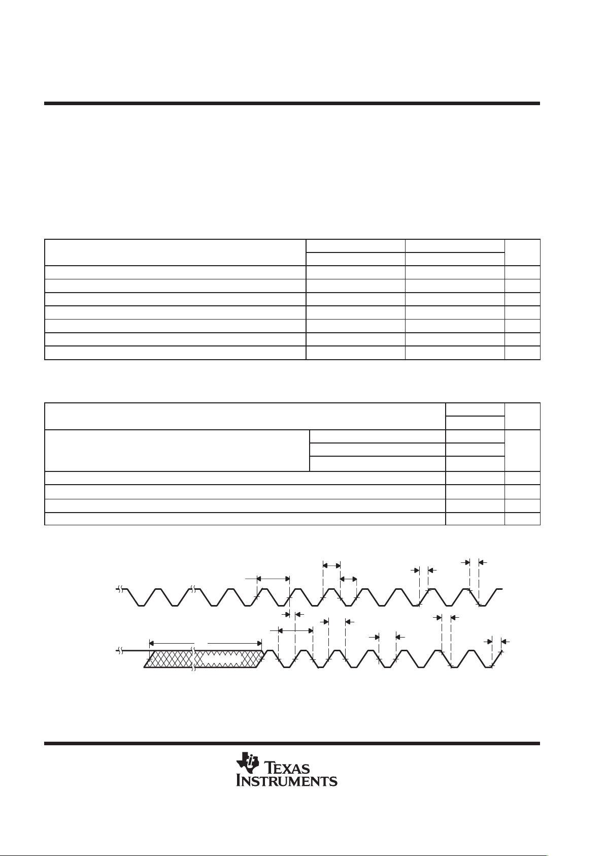
TMS320VC5409
FIXED-POINT DIGITAL SIGNAL PROCESSOR
SPRS082C – APRIL 1999 – REVISED MARCH 2000
42
POST OFFICE BOX 1443 • HOUSTON, TEXAS 77251–1443
multiply-by-N clock option (PLL enabled)
The frequency of the reference clock provided at the X2/CLKIN pin can be multiplied by a factor of N to generate
the internal machine cycle. The selection of the clock mode and the value of N is described in the clock generator
section.
When an external clock source is used, the external frequency injected must conform to specifications listed
in the timing requirements table.
switching characteristics over recommended operating conditions [H = 0.5t
c(CO)
]
(see Figure 12 and Figure 14)
’5409-80 ’5409-100
PARAMETER
MIN TYP MAX MIN TYP MAX
UNIT
t
c(CO)
Cycle time, CLKOUT 12.5 t
c(CI)
/N
†
10 t
c(CI)
/N
†
ns
t
d(CI-CO)
Delay time, X2/CLKIN high/low to CLKOUT high/low 4 10 17 4 10 17 ns
t
f(CO)
Fall time, CLKOUT 2 2 ns
t
r(CO)
Rise time, CLKOUT 2 2 ns
t
w(COL)
Pulse duration, CLKOUT low H–3 H–1 H H–2 H–1 H ns
t
w(COH)
Pulse duration, CLKOUT high H–3 H–1 H H–2 H–1 H ns
t
p
Transitory phase, PLL lock up time 30 30
s
†
N = Multiplication factor
timing requirements (see Figure 14)
†
’5409-80,-100
MIN MAX
UNIT
Integer PLL multiplier N (N = 1–15) 20
‡
200
t
c(CI
)
Cycle time, X2/CLKIN
PLL multiplier N = x.5
20
‡
100
ns
t
c(CI)
Cycle time, X2/CLKIN
PLL multiplier N = x.25, x.75 20
‡
50
ns
t
f(CI)
Fall time, X2/CLKIN 8 ns
t
r(CI)
Rise time, X2/CLKIN 8 ns
tw(CIL) Pulse duration, X2/CLKIN low 5 ns
tw(CIH) Pulse duration, X2/CLKIN high 5 ns
†
N = Multiplication factor
‡
The multiplication factor and minimum X2/CLKIN cycle time should be chosen such that the resulting CLKOUT cycle time is within the specified
range (tc(CO))
t
c(CO)
t
c(CI)
t
w(COH)
t
f(CO)
t
r(CO)
t
f(CI)
X2/CLKIN
CLKOUT
t
d(CI-CO)
t
w(COL)
t
r(CI)
tp
Unstable
t
w(CIH)
t
w(CIL)
Figure 14. External Multiply-by-One Clock Timing

TMS320VC5409
FIXED-POINT DIGITAL SIGNAL PROCESSOR
SPRS082C – APRIL 1999 – REVISED MARCH 2000
43
POST OFFICE BOX 1443 • HOUSTON, TEXAS 77251–1443
memory and parallel I/O interface timing
switching characteristics over recommended operating conditions for a memory read
(MSTRB
= 0)
†
(see Figure 15)
’5409-80,-100
PARAMETER
MIN MAX
UNIT
t
d(CLKL-A)
Delay time, CLKOUT low to address valid
‡
0 3 ns
t
d(CLKH-A)
Delay time, CLKOUT high (transition) to address valid
§
0 3 ns
t
d(CLKL-MSL)
Delay time, CLKOUT l ow to MSTRB low 0 3 ns
t
d(CLKL-MSH)
Delay time, CLKOUT low to MSTRB high 0 3 ns
t
h(CLKL-A)R
Hold time, address valid after CLKOUT low
‡
0 3 ns
t
h(CLKH-A)R
Hold time, address valid after CLKOUT high
§
0 3 ns
†
Address, PS
, and DS timings are all included in timings referenced as address.
‡
In the case of a memory read preceded by a memory read
§
In the case of a memory read preceded by a memory write
timing requirements for a memory read (MSTRB = 0) [H = 0.5 t
c(CO)
]
†
(see Figure 15)
’5409-80,-100
MIN MAX
UNIT
t
a(A)M
Access time, read data access from address valid 2H–10
¶
ns
t
a(MSTRBL)
Access time, read data access from MSTRB low 2H–10
¶
ns
t
su(D)R
Setup time, read data before CLKOUT low 8 ns
t
h(D)R
Hold time, read data after CLKOUT low 0 ns
t
h(A-D)R
Hold time, read data after address invalid 0 ns
t
h(D)MSTRBH
Hold time, read data after MSTRB high 1 ns
†
Address, PS, and DS timings are all included in timings referenced as address.
¶
This access timing reflects a zero wait-state timing.

TMS320VC5409
FIXED-POINT DIGITAL SIGNAL PROCESSOR
SPRS082C – APRIL 1999 – REVISED MARCH 2000
44
POST OFFICE BOX 1443 • HOUSTON, TEXAS 77251–1443
memory and parallel I/O interface timing (continued)
PS, DS
R/W
MSTRB
D[15:0]
A[22:0]
CLKOUT
t
h(D)R
t
h(CLKL-A)R
t
d(CLKL-MSH)
t
d(CLKL-A)
t
d(CLKL-MSL)
t
su(D)R
t
a(A)M
t
a(MSTRBL)
t
h(A-D)R
t
h(D)MSTRBH
NOTE A: A[22:16] apply to DMA accesses to extended I/O, DATA, PROGRAM memory. The CPU has access to only extended
PROGRAM memory.
Figure 15. Memory Read (MSTRB = 0)
TMS320VC5409
FIXED-POINT DIGITAL SIGNAL PROCESSOR
SPRS082C – APRIL 1999 – REVISED MARCH 2000
45
POST OFFICE BOX 1443 • HOUSTON, TEXAS 77251–1443
memory and parallel I/O interface timing (continued)
switching characteristics over recommended operating conditions for a memory write
(MSTRB
= 0) [H = 0.5 t
c(CO)
]† (see Figure 16)
’5409-80,-100
PARAMETER
MIN MAX
UNIT
t
d(CLKH-A)
Delay time, CLKOUT high to address valid
‡
0 3 ns
t
d(CLKL-A)
Delay time, CLKOUT l ow to addres s valid
§
0 3 ns
t
d(CLKL-MSL)
Delay time, CLKOUT l ow to MSTRB low 0 3 ns
t
d(CLKL-D)W
Delay time, CLKOUT l ow to data valid 0 8 ns
t
d(CLKL-MSH)
Delay time, CLKOUT l ow to MSTRB high 0 3 ns
t
d(CLKH-RWL)
Delay time, CLKOUT high to R/W low 0 4 ns
t
d(CLKH-RWH)
Delay time, CLKOUT high to R/W high 0 4 ns
t
d(RWL-MSTRBL)
Delay time, R/W low to MSTRB low H – 2 H + 1 ns
t
h(A)W
Hold time, address valid after CLKOUT high
‡
0 3 ns
t
h(D)MSH
Hold time, write data valid after MSTRB high H–3 H+6
§
ns
t
w(SL)MS
Pulse duration, MSTRB low 2H–2 ns
t
su(A)W
Setup time, address valid before MSTRB low 2H–2 ns
t
su(D)MSH
Setup time, write data valid before MSTRB high 2H–6 2H+6
§
ns
t
en(D–RWL)
Enable time, data bus driven after R/W low H–5 ns
t
dis(RWH–D)
Disable time, R/W high to data bus high impedance 0 ns
†
Address, PS, and DS timings are all included in timings referenced as address.
‡
In the case of a memory write preceded by a memory write
§
In the case of a memory write preceded by an I/O cycle
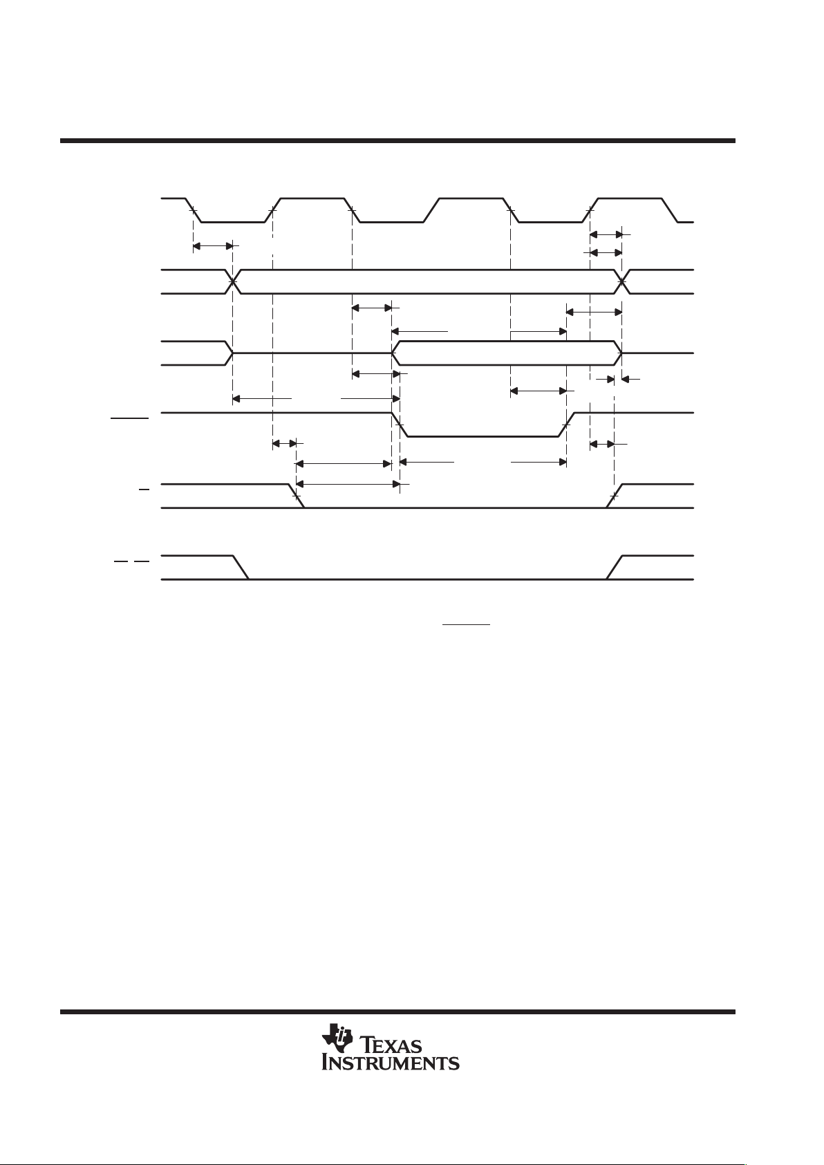
TMS320VC5409
FIXED-POINT DIGITAL SIGNAL PROCESSOR
SPRS082C – APRIL 1999 – REVISED MARCH 2000
46
POST OFFICE BOX 1443 • HOUSTON, TEXAS 77251–1443
memory and parallel I/O interface timing (continued)
PS, DS
R/W
MSTRB
D[15:0]
A[22:0]
CLKOUT
t
d(CLKH-RWH)
t
h(A)W
t
d(CLKL-MSH)
t
su(D)MSH
t
d(CLKL-D)W
t
w(SL)MS
t
su(A)W
t
d(CLKL-MSL)
t
h(D)MSH
t
d(CLKL-A)
t
d(CLKH-RWL)
t
d(RWL-MSTRBL)
t
d(CLKH-A)
t
en(D-RWL)
t
dis(RWH-D)
NOTE A: A[22:16] apply to DMA accesses to extended I/O, DATA, PROGRAM memory. The CPU has access to only extended
PROGRAM memory.
Figure 16. Memory Write (MSTRB = 0)
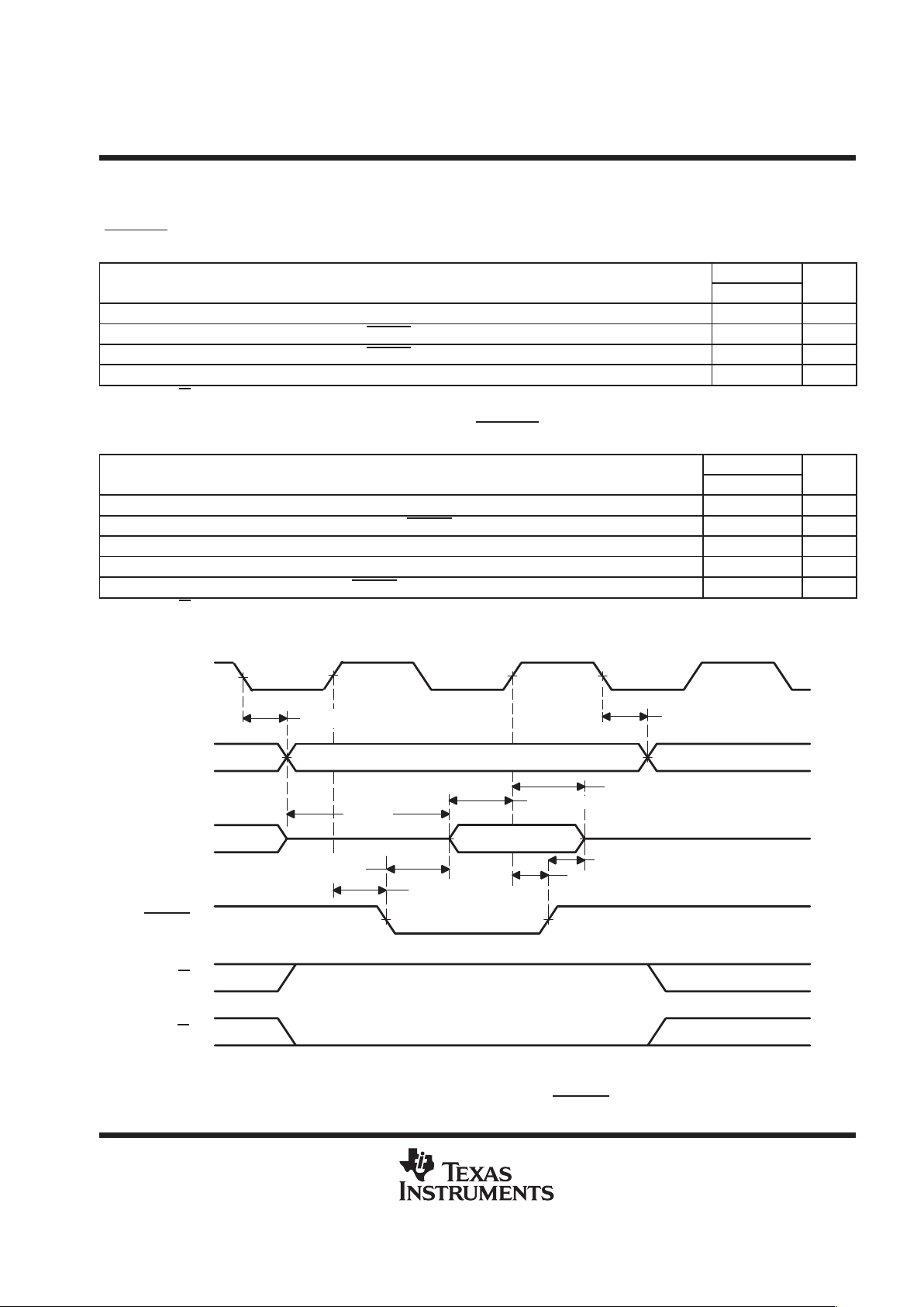
TMS320VC5409
FIXED-POINT DIGITAL SIGNAL PROCESSOR
SPRS082C – APRIL 1999 – REVISED MARCH 2000
47
POST OFFICE BOX 1443 • HOUSTON, TEXAS 77251–1443
memory and parallel I/O interface timing (continued)
switching characteristics over recommended operating conditions for a parallel I/O port read
(IOSTRB
= 0)† (see Figure 17)
’5409-80,-100
PARAMETER
MIN MAX
UNIT
t
d(CLKL-A)
Delay time, CLKOUT low to address valid 0 3 ns
t
d(CLKH-ISTRBL)
Delay time, CLKOUT h igh to IOSTR B low 0 3 ns
t
d(CLKH-ISTRBH)
Delay time, CLKOUT h igh to IOSTR B high 0 3 ns
t
h(A)IOR
Hold time, address after CLKOUT low 0 3 ns
†
Address and IS timings are included in timings referenced as address.
timing requirements for a parallel I/O port read (IOSTRB = 0) [H = 0.5 t
c(CO)
]† (see Figure 17)
’5409-80,-100
MIN MAX
UNIT
t
a(A)IO
Access time, read data access from address valid
‡
3H–9 ns
t
a(ISTRBL)IO
Access time, read data access from IOSTRB low
‡
2H–8 ns
t
su(D)IOR
Setup time, read data before CLKOUT high 8 ns
t
h(D)IOR
Hold time, read data after CLKOUT high 0 ns
t
h(ISTRBH-D)R
Hold time, read data after IOSTRB high 0 ns
†
Address and IS timings are included in timings referenced as address.
‡
This access timing reflects a zero wait-state timing.
IS
R/W
IOSTRB
D[15:0]
A[22:0]
CLKOUT
t
h(A)IOR
t
d(CLKH-ISTRBH)
t
h(D)IOR
t
su(D)IOR
t
a(A)IO
t
d(CLKH-ISTRBL)
t
d(CLKL-A)
t
a(ISTRBL)IO
t
h(ISTRBH-D)R
NOTE A: A[22:16] apply to DMA accesses to extended I/O, DATA, PROGRAM memory. The CPU has access to only extended
PROGRAM memory.
Figure 17. Parallel I/O Port Read (IOSTRB = 0)

TMS320VC5409
FIXED-POINT DIGITAL SIGNAL PROCESSOR
SPRS082C – APRIL 1999 – REVISED MARCH 2000
48
POST OFFICE BOX 1443 • HOUSTON, TEXAS 77251–1443
memory and parallel I/O interface timing (continued)
switching characteristics over recommended operating conditions for a
parallel I/O port write
(IOSTRB
= 0)
[H = 0.5 t
c(CO)
]† (see Figure 18)
’5409-80,-100
PARAMETER
MIN MAX
UNIT
t
d(CLKL-A)
Delay time, CLKOUT low to address valid 0 3 ns
t
d(CLKH-ISTRBL)
Delay time, CLKOUT h igh to IOSTR B low 0 3 ns
t
d(CLKH-D)IOW
Delay time, CLKOUT h i gh to write data valid H–5 H+8 ns
t
d(CLKH-ISTRBH)
Delay time, CLKOUT h igh to IOSTR B high 0 3 ns
t
d(CLKL-RWL)
Delay time, CLKOUT low to R/W low 0 3 ns
t
d(CLKL-RWH)
Delay time, CLKOUT low to R/W high 0 3 ns
t
h(A)IOW
Hold time, address valid after CLKOUT low 0 3 ns
t
h(D)IOW
Hold time, write data after IOSTRB high H–3 H+7 ns
t
su(D)IOSTRBH
Setup time, write data before IOSTRB high H–7 H+1 ns
t
su(A)IOSTRBL
Setup time, address valid before IOSTRB low H–2 H+2 ns
†
Address and IS timings are included in timings referenced as address.
IS
R/W
IOSTRB
D[15:0]
A[22:0]
CLKOUT
t
d(CLKH-ISTRBH)
t
h(A)IOW
t
h(D)IOW
t
d(CLKH-D)IOW
t
d(CLKH-ISTRBL)
t
d(CLKL-A)
t
d(CLKL-RWL)
t
d(CLKL-RWH)
t
su(A)IOSTRBL
t
su(D)IOSTRBH
NOTE A: A[22:16] apply to DMA accesses to extended I/O, DATA, PROGRAM memory. The CPU has access to only extended
PROGRAM memory.
Figure 18. Parallel I/O Port Write (IOSTRB = 0)

TMS320VC5409
FIXED-POINT DIGITAL SIGNAL PROCESSOR
SPRS082C – APRIL 1999 – REVISED MARCH 2000
49
POST OFFICE BOX 1443 • HOUSTON, TEXAS 77251–1443
ready timing for externally generated wait states
timing requirements for externally generated wait states [H = 0.5 t
c(CO)
]† (see Figure 19, Figure 20,
Figure 21, and Figure 22)
’5409-80,-100
MIN MAX
UNIT
t
su(RDY)
Setup time, READY before CLKOUT low 7 ns
t
h(RDY)
Hold time, READY after CLKOUT low 0 ns
t
v(RDY)MSTRB
Valid time, READY after MSTRB low
‡
4H–9 ns
t
h(RDY)MSTRB
Hold time, READY after MSTRB low
‡
4H ns
t
v(RDY)IOSTRB
Valid time, READY after IOSTRB low
‡
5H–9 ns
t
h(RDY)IOSTRB
Hold time, READY after IOSTRB low
‡
5H ns
t
v(MSCL)
Valid time, MSC low after CLKOUT low 0 3 ns
t
v(MSCH)
Valid time, MSC high after CLKOUT low 0 3 ns
†
The hardware wait states can be used only in conjunction with the software wait states to extend the bus cycles. To generate wait states using
READY, at least two software wait states must be programmed.
‡
These timings are included for reference only. The critical timings for READY are those referenced to CLKOUT.
MSC
MSTRB
READY
A[22:0]
CLKOUT
t
v(MSCH)
t
v(MSCL)
t
h(RDY)
t
h(RDY)MSTRB
t
v(RDY)MSTRB
Wait State
Generated
by READY
Wait States
Generated Internally
t
su(RDY)
NOTE A: A[22:16] apply to DMA accesses to extended I/O, DATA, PROGRAM memory. The CPU has access to only extended
PROGRAM memory.
Figure 19. Memory Read With Externally Generated Wait States
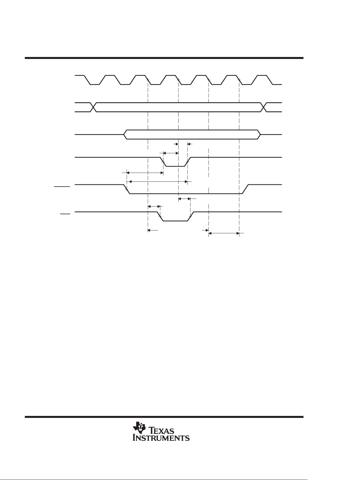
TMS320VC5409
FIXED-POINT DIGITAL SIGNAL PROCESSOR
SPRS082C – APRIL 1999 – REVISED MARCH 2000
50
POST OFFICE BOX 1443 • HOUSTON, TEXAS 77251–1443
ready timing for externally generated wait states (continued)
MSC
MSTRB
READY
D[15:0]
A[22:0]
CLKOUT
t
v(MSCH)
t
h(RDY)
Wait State Generated
by READY
Wait States
Generated Internally
t
h(RDY)MSTRB
t
v(RDY)MSTRB
t
v(MSCL)
t
su(RDY)
NOTE A: A[22:16] apply to DMA accesses to extended I/O, DATA, PROGRAM memory. The CPU has access to only extended
PROGRAM memory.
Figure 20. Memory Write With Externally Generated Wait States

TMS320VC5409
FIXED-POINT DIGITAL SIGNAL PROCESSOR
SPRS082C – APRIL 1999 – REVISED MARCH 2000
51
POST OFFICE BOX 1443 • HOUSTON, TEXAS 77251–1443
ready timing for externally generated wait states (continued)
t
su(RDY)
MSC
IOSTRB
READY
A[22:0]
CLKOUT
t
v(MSCH)
t
h(RDY)
Wait State Generated
by READY
Wait
States
Generated
Internally
t
v(RDY)IOSTRB
t
v(MSCL)
t
h(RDY)IOSTRB
NOTE A: A[22:16] apply to DMA accesses to extended I/O, DATA, PROGRAM memory. The CPU has access to only extended
PROGRAM memory.
Figure 21. I/O Read With Externally Generated Wait States

TMS320VC5409
FIXED-POINT DIGITAL SIGNAL PROCESSOR
SPRS082C – APRIL 1999 – REVISED MARCH 2000
52
POST OFFICE BOX 1443 • HOUSTON, TEXAS 77251–1443
ready timing for externally generated wait states (continued)
IOSTRB
MSC
READY
D[15:0]
A[22:0]
CLKOUT
t
h(RDY)
Wait State Generated
by READY
Wait States
Generated
Internally
t
v(RDY)IOSTRB
t
su(RDY)
t
v(MSCH)
t
v(MSCL)
t
h(RDY)IOSTRB
NOTE A: A[22:16] apply to DMA accesses to extended I/O, DATA, PROGRAM memory. The CPU has access to only extended
PROGRAM memory.
Figure 22. I/O Write With Externally Generated Wait States

TMS320VC5409
FIXED-POINT DIGITAL SIGNAL PROCESSOR
SPRS082C – APRIL 1999 – REVISED MARCH 2000
53
POST OFFICE BOX 1443 • HOUSTON, TEXAS 77251–1443
HOLD and HOLDA timings
switching characteristics over recommended operating conditions for memory control signals
and HOLDA
, [H = 0.5 t
c(CO)
] (see Figure 23)
’5409-80, -100
PARAMETER
MIN MAX
UNIT
t
dis(CLKL-A)
Disable time, address, PS, DS, IS high impedance from CLKOUT low 5 ns
t
dis(CLKL-RW)
Disable time, R/W high impedance from CLKOUT low 5 ns
t
dis(CLKL-S)
Disable time, MSTRB, IOSTRB high impedance from CLKOUT low 5 ns
t
en(CLKL-A)
Enable time, address, PS, DS, IS from CLKOUT low 2H+5 ns
t
en(CLKL-RW)
Enable time, R/W enabled from CLKOUT low 2H+5 ns
t
en(CLKL-S)
Enable time, MSTRB, IOSTRB enabled from CLKOUT low 1 2H+5 ns
Valid time, HOLDA low after CLKOUT low
0 4 ns
t
v(HOLDA)
Valid time, HOLDA high after CLKOUT low
0 4 ns
t
w(HOLDA)
Pulse duration, HOLDA low duration 2H–1 ns
timing requirements for memory control signals and HOLD, [H = 0.5 t
c(CO)
] (see Figure 23)
’5409-80, -100
MIN MAX
UNIT
t
w(HOLD)
Pulse duration, HOLD low 4H+8 ns
t
su(HOLD)
Setup time, HOLD low/high before CLKOUT low 8 ns

TMS320VC5409
FIXED-POINT DIGITAL SIGNAL PROCESSOR
SPRS082C – APRIL 1999 – REVISED MARCH 2000
54
POST OFFICE BOX 1443 • HOUSTON, TEXAS 77251–1443
HOLD and HOLDA timings (continued)
IOSTRB
MSTRB
R/W
D[15:0]
PS
, DS, IS
A[22:0]
HOLDA
HOLD
CLKOUT
t
en(CLKL-S)
t
en(CLKL-S)
t
en(CLKL-RW)
t
dis(CLKL-S)
t
dis(CLKL-S)
t
dis(CLKL-RW)
t
dis(CLKL-A)
t
v(HOLDA)
t
v(HOLDA)
t
w(HOLDA)
t
w(HOLD)
t
su(HOLD)
t
su(HOLD)
t
en(CLKL-A)
NOTE A: A[22:16] apply to DMA accesses to extended I/O, DATA, PROGRAM memory. The CPU has access to only extended
PROGRAM memory.
Figure 23. HOLD and HOLDA Timings (HM = 1)
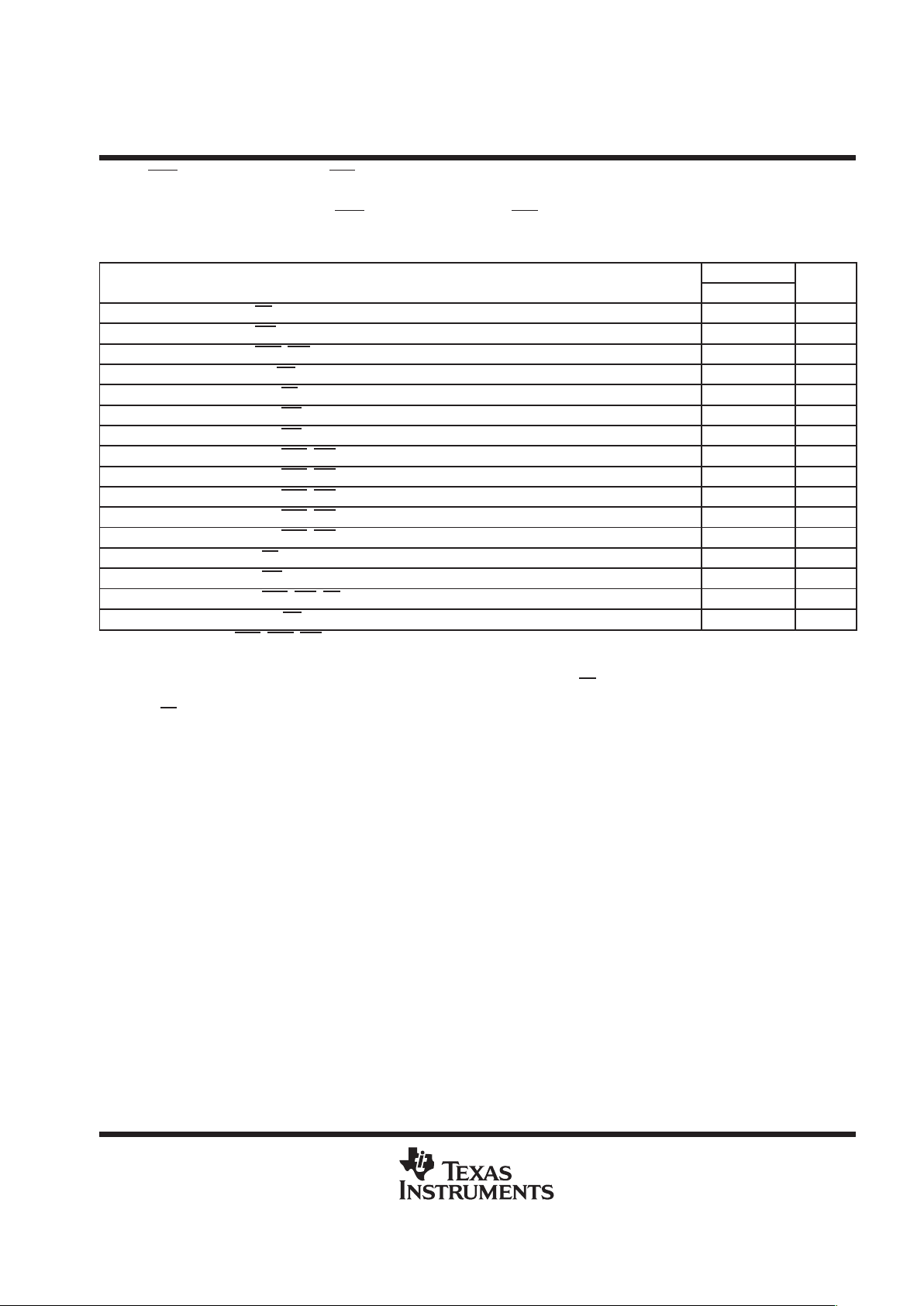
TMS320VC5409
FIXED-POINT DIGITAL SIGNAL PROCESSOR
SPRS082C – APRIL 1999 – REVISED MARCH 2000
55
POST OFFICE BOX 1443 • HOUSTON, TEXAS 77251–1443
reset, BIO, interrupt, and MP/MC timings
timing requirements for reset, BIO, interrupt, and MP/MC [H = 0.5 t
c(CO)
] (see Figure 24, Figure 25,
and Figure 26)
’5409-80, -100
MIN MAX
UNIT
t
h(RS)
Hold time, RS after CLKOUT low 0 ns
t
h(BIO)
Hold time, BIO after CLKOUT low 0 ns
t
h(INT)
Hold time, INTn, NMI, after CLKOUT low
†
0 ns
t
h(MPMC)
Hold time, MP/MC after CLKOUT low 0 ns
t
w(RSL)
Pulse duration, RS low
‡§
4H+4 ns
t
w(BIO)S
Pulse duration, BIO low, synchronous 2H+1 ns
t
w(BIO)A
Pulse duration, BIO low, asynchronous 4H ns
t
w(INTH)S
Pulse duration, INTn, NMI high (synchronous) 2H+1 ns
t
w(INTH)A
Pulse duration, INTn, NMI high (asynchronous) 4H ns
t
w(INTL)S
Pulse duration, INTn, NMI low (synchronous) 2H+1 ns
t
w(INTL)A
Pulse duration, INTn, NMI low (asynchronous) 4H ns
t
w(INTL)WKP
Pulse duration, INTn, NMI low for IDLE2/IDLE3 wakeup 8 ns
t
su(RS)
Setup time, RS before X2/CLKIN low
¶
6 ns
t
su(BIO)
Setup time, BIO before CLKOUT low 7 10 ns
t
su(INT)
Setup time, INTn, NMI, RS before CLKOUT low 8 10 ns
t
su(MPMC)
Setup time, MP/MC before CLKOUT low 8 ns
†
The external interrupts (INT0–INT3, NMI) are synchronized to the core CPU by way of a two-flip-flop synchronizer which samples these inputs
with consecutive falling edges of CLKOUT. The input to the interrupt pins is required to represent a 1-0-0 sequence at the timing that is
corresponding to three CLKOUT sampling sequences.
‡
If the PLL mode is selected, then at power-on sequence, or at wakeup from IDLE3, RS
must be held low for at least 50 µs to ensure
synchronization and lock-in of the PLL.
§
Note that RS
may cause a change in clock frequency, therefore changing the value of H.
¶
Divide-by-two mode
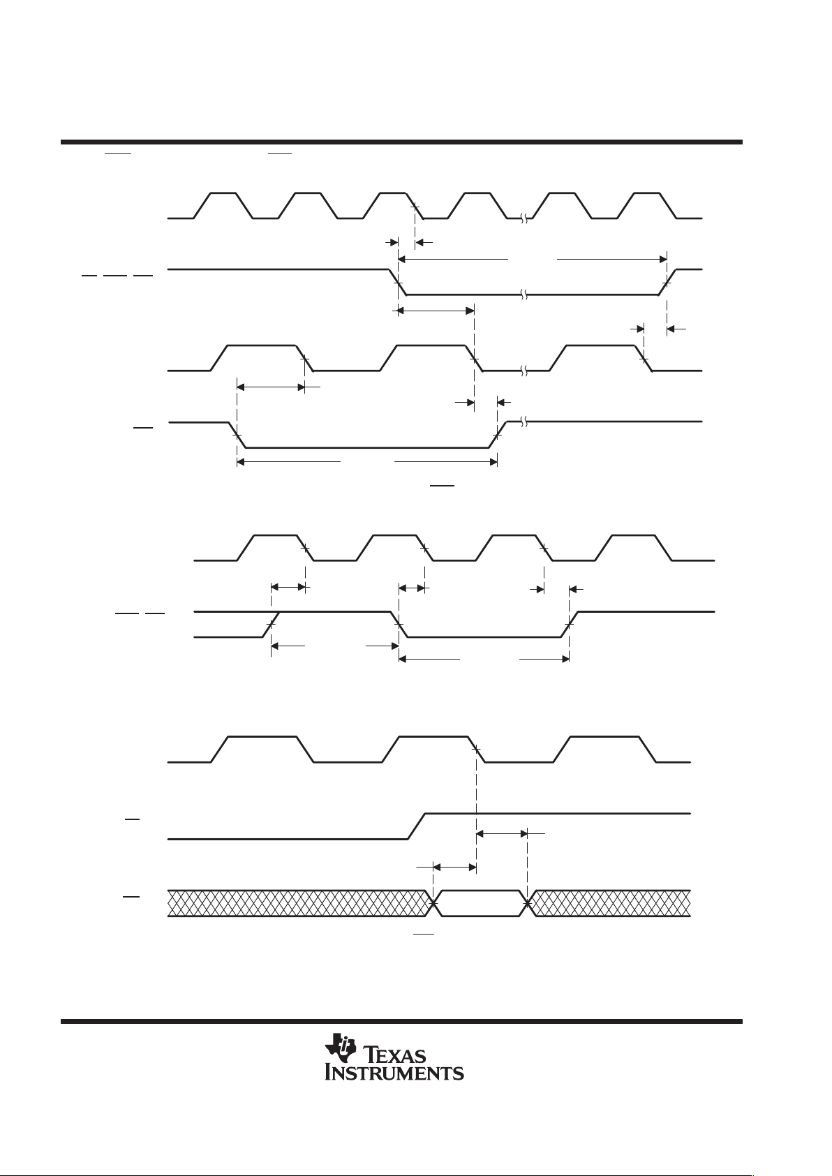
TMS320VC5409
FIXED-POINT DIGITAL SIGNAL PROCESSOR
SPRS082C – APRIL 1999 – REVISED MARCH 2000
56
POST OFFICE BOX 1443 • HOUSTON, TEXAS 77251–1443
reset, BIO, interrupt, and MP/MC timings (continued)
BIO
CLKOUT
RS
, INTn, NMI
X2/CLKIN
t
h(BIO)
t
h(RS)
t
su(INT)
t
w(BIO)S
t
su(BIO)
t
w(RSL)
t
su(RS)
Figure 24. Reset and BIO Timings
INTn, NMI
CLKOUT
t
h(INT)
t
su(INT)
t
su(INT)
t
w(INTL)A
t
w(INTH)A
Figure 25. Interrupt Timing
MP/MC
RS
CLKOUT
t
su(MPMC)
t
h(MPMC)
Figure 26. MP/MC Timing
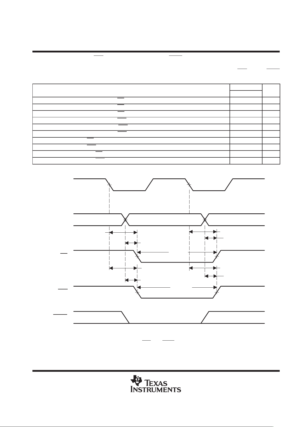
TMS320VC5409
FIXED-POINT DIGITAL SIGNAL PROCESSOR
SPRS082C – APRIL 1999 – REVISED MARCH 2000
57
POST OFFICE BOX 1443 • HOUSTON, TEXAS 77251–1443
instruction acquisition (IAQ), interrupt acknowledge (IACK), external flag (XF), and TOUT timings
switching characteristics over recommended operating conditions for IAQ and IACK
[H = 0.5 t
c(CO)
] (see Figure 27)
’5409-80, -100
PARAMETER
MIN MAX
UNIT
t
d(CLKL-IAQL)
Delay time, CLKOUT low to IAQ low 0 3 ns
t
d(CLKL-IAQH)
Delay time, CLKOUT low to IAQ high 0 3 ns
t
d(A)IAQ
Delay time, address valid to IAQ low 1 ns
t
d(CLKL-IACKL)
Delay time, CLKOUT low to IACK low 0 3 ns
t
d(CLKL-IACKH)
Delay time , CLKOUT low to IACK high 0 3 ns
t
d(A)IACK
Delay time, address valid to IACK low 1 ns
t
h(A)IAQ
Hold time, IAQ high after address invalid – 2 ns
t
h(A)IACK
Hold time, IACK high after address invalid – 2 ns
t
w(IAQL)
Pulse duration, IAQ low 2H–2 ns
t
w(IACKL)
Pulse duration, IACK low 2H–2 ns
MSTRB
IACK
IAQ
A[22:0]
CLKOUT
t
d(A)IACK
t
d(A)IAQ
t
w(IACKL)
t
h(A)IACK
t
d(CLKL-IACKL)
t
w(IAQL)
t
h(A)IAQ
t
d(CLKL-IAQL)
t
d(CLKL-IACKH)
t
d(CLKL-IAQH)
NOTE A: A[22:16] apply to DMA accesses to extended I/O, DATA, PROGRAM memory. The CPU has access to only extended
PROGRAM memory.
Figure 27. IAQ and IACK Timings

TMS320VC5409
FIXED-POINT DIGITAL SIGNAL PROCESSOR
SPRS082C – APRIL 1999 – REVISED MARCH 2000
58
POST OFFICE BOX 1443 • HOUSTON, TEXAS 77251–1443
instruction acquisition (IAQ), interrupt acknowledge (IACK), external flag (XF), and TOUT timings
(continued)
switching characteristics over recommended operating conditions for XF and TOUT
[H = 0.5 t
c(CO)
] (see Figure 28 and Figure 29)
’5409-80, -100
PARAMETER
MIN MAX
UNIT
Delay time, CLKOUT low to XF high 0 2
t
d(XF)
Delay time, CLKOUT low to XF low 0 2
ns
t
d(TOUTH)
Delay time, CLKOUT low to TOUT high 0 4 ns
t
d(TOUTL)
Delay time, CLKOUT low to TOUT low 0 4 ns
t
w(TOUT)
Pulse duration, TOUT 2H ns
XF
CLKOUT
t
d(XF)
Figure 28. XF Timing
TOUT
CLKOUT
t
w(TOUT)
t
d(TOUTL)
t
d(TOUTH)
Figure 29. TOUT Timing

TMS320VC5409
FIXED-POINT DIGITAL SIGNAL PROCESSOR
SPRS082C – APRIL 1999 – REVISED MARCH 2000
59
POST OFFICE BOX 1443 • HOUSTON, TEXAS 77251–1443
multichannel buffered serial port timing
timing requirements for the McBSP† [H=0.5t
c(CO)
] (see Figure 30 and Figure 31)
MIN MAX UNIT
t
c(BCKRX)
Cycle time, BCLKR/X BCLKR/X ext 4H ns
t
w(BCKRX)
Pulse duration, BCLKR/X or BCLKR/X high BCLKR/X ext 2H–1 ns
BCLKR int 0
t
h(BCKRL-BFRH)
Hold time, external BFSR high after BCLKR low
BCLKR ext
4
ns
BCLKR int 0
t
h(BCKRL-BDRV)
Hold time, BDR valid after BCLKR low
BCLKR ext
4
ns
BCLKX int 0
t
h(BCKXL-BFXH)
Hold time, external BFSX high after BCLKX low
BCLKX ext
4
ns
BCLKR int 7
t
su(BFRH-BCKRL)
Setup time, external BFSR high before BCLKR low
BCLKR ext
2
ns
BCLKR int 7
t
su(BDRV-BCKRL)
Setup time, BDR valid before BCLKR low
BCLKR ext
2
ns
BCLKX int 7
t
su(BFXH-BCKXL)
Setup time, external BFSX high before BCLKX low
BCLKX ext
2
ns
t
r(BCKRX)
Rise time, BCKR/X BCLKR/X ext 8 ns
t
f(BCKRX)
Fall time, BCKR/X BCLKR/X ext 8 ns
†
Polarity bits CLKRP = CLKXP = FSRP = FSXP = 0. If the polarity of any of the signals is inverted, then the timing references of that signal are
also inverted.
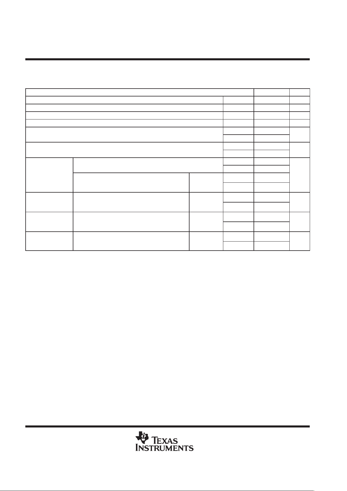
TMS320VC5409
FIXED-POINT DIGITAL SIGNAL PROCESSOR
SPRS082C – APRIL 1999 – REVISED MARCH 2000
60
POST OFFICE BOX 1443 • HOUSTON, TEXAS 77251–1443
multichannel buffered serial port timing (continued)
switching characteristics for the McBSP
†
[H=0.5t
c(CO)
] (see Figure 30 and Figure 31)
PARAMETER MIN MAX UNIT
t
c(BCKRX)
Cycle time, BCLKR/X BCLKR/X int 4H ns
t
w(BCKRXH)
Pulse duration, BCLKR/X high BCLKR/X int D–3‡D+1
‡
ns
t
w(BCKRXL)
Pulse duration, BCLKR/X low BCLKR/X int C–3‡C+1
‡
ns
t
d(BCKRH-BFRV)
Delay time, BCLKR high to internal BFSR valid BCLKR int –2 2 ns
BCLKX int 0 6
t
d(BCKXH-BFXV)
Delay time, BCLKX high to internal BFSX valid
BCLKX ext
4 12
ns
BCLKX int –4 7
t
dis(BCKXH-BDXHZ)
Disable time, BCLKX high to BDX high impedance following last data bit
BCLKX ext
3 9
ns
Delay time, BCLKX high to BDX valid. This applies to all bits except the first
BCLKX int 0 7
Delay time, BCLKX high to BDX valid. This a lies to all bits exce t the first
bit transmitted.
BCLKX ext 4 12
t
d(BCKXH-BDXV)
Delay time, BCLKX high to BDX valid.
¶§
pp
BCLKX int 7
ns
Only applies to first bit transmitted when in Data Delay 1
or 2 (XDATDLY=01b or 10b) modes
DXENA = 0
BCLKX ext 12
Enable time, BCLKX high to BDX driven.
¶§
pp
BCLKX int –4
t
e(BCKXH-BDX)
Only applies to first bit transmitted when in Data Delay 1
or 2 (XDATDLY=01b or 10b) modes
DXENA = 0
BCLKX ext 2
ns
Delay time, BFSX high to BDX valid.
¶§
pp
BFSX int 2
t
d(BFXH-BDXV)
Only applies to first bit transmitted when in Data Delay 0
(XDATDLY=00b) mode.
DXENA = 0
BFSX ext 12
ns
Enable time, BFSX high to BDX driven.
¶§
pp
BFSX int –1
t
e(BFXH-BDX)
Only applies to first bit transmitted when in Data Delay 0
(XDATDLY=00b) mode
DXENA = 0
BFSX ext 2
ns
†
Polarity bits CLKRP = CLKXP = FSRP = FSXP = 0. If the polarity of any of the signals is inverted, then the timing references of that signal are
also inverted.
‡
T=BCLKRX period = (1 + CLKGDV) * 2H
C=BCLKRX low pulse width = T/2 when CLKGDV is odd or zero and = (CLKGDV/2) * 2H when CLKGDV is even
D=BCLKRX high pulse width = T/2 when CLKGDV is odd or zero and = (CLKGDV/2 + 1) * 2H when CLKGDV is even
§
See the
TMS320C54x Enhanced Peripherals Reference Set, Volume 5
(literature number SPRU302) for a description of the DX enable (DXENA)
and data delay features of the McBSP.
¶
The transmit delay enable (DXENA) and A-bis mode (ABIS) features of the McBSP are not implemented on the TMS320VC5409.
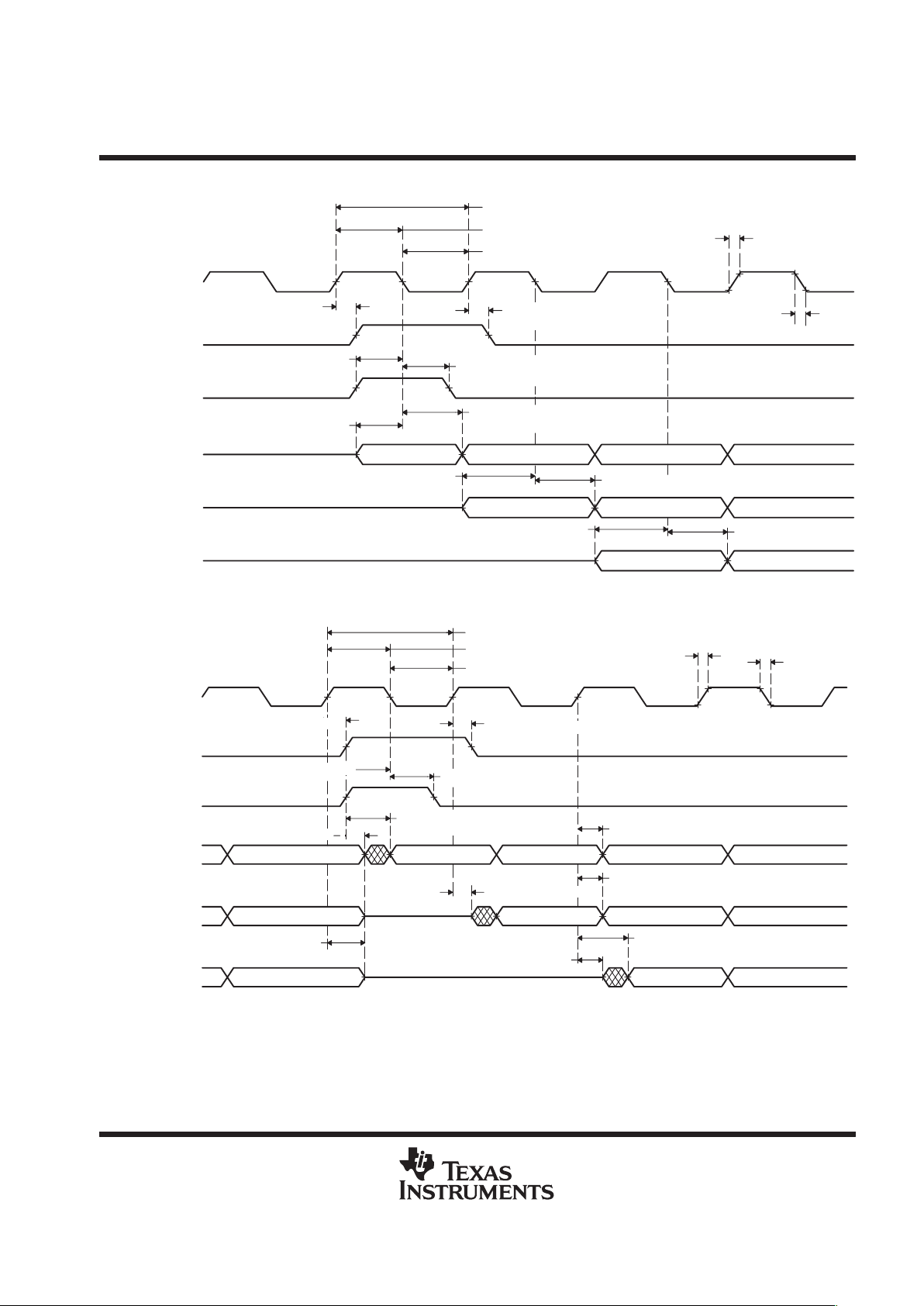
TMS320VC5409
FIXED-POINT DIGITAL SIGNAL PROCESSOR
SPRS082C – APRIL 1999 – REVISED MARCH 2000
61
POST OFFICE BOX 1443 • HOUSTON, TEXAS 77251–1443
multichannel buffered serial port timing (continued)
(n–2)Bit (n–1)
(n–3)(n–2)Bit (n–1)
(n–4)(n–3)(n–2)Bit (n–1)
t
h(BCKRL–BDRV)
t
su(BDRV–BCKRL)
t
h(BCKRL–BDRV)
t
su(BDRV–BCKRL)
t
su(BDRV–BCKRL)
t
h(BCKRL–BDRV)
t
h(BCKRL–BFRH)
t
su(BFRH–BCKRL)
t
d(BCKRH–BFRV)
t
d(BCKRH–BFRV)
t
r(BCKRX)
t
r(BCKRX)
t
w(BCKRXL)
t
c(BCKRX)
t
w(BCKRXH)
(RDATDLY=10b)
BDR
(RDATDLY=01b)
BDR
(RDATDLY=00b)
BDR
BFSR (ext)
BFSR (int)
BCLKR
Figure 30. McBSP Receive Timings
t
e(BCKXH–BDX)
t
d(BCKXH–BDXV)
t
d(BCKXH–BDXV)
t
e(BCKXH–BDX)
t
dis(BCKXH–BDXHZ)
t
d(BCKXH–BDXV)
t
d(BDFXH–BDXV)
t
e(BDFXH–BDX)
(XDATDLY=10b)
BDX
(XDATDLY=01b)
BDX
(XDATDLY=00b)
BDX
(n–2)Bit (n–1)Bit 0
(n–4)Bit (n–1) (n–3)(n–2)
Bit 0
(n–3)(n–2)Bit (n–1)
Bit 0
t
h(BCKXL–BFXH)
t
f(BCKRX)
t
r(BCKRX)
t
w(BCKRXL)
t
c(BCKRX)
t
w(BCKRXH)
BFSX (ext)
BFSX (int)
BCLKX
t
d(BCKXH–BFXV)
t
d(BCKXH–BFXV)
t
su(BFXH–BCKXL)
Figure 31. McBSP Transmit Timings

TMS320VC5409
FIXED-POINT DIGITAL SIGNAL PROCESSOR
SPRS082C – APRIL 1999 – REVISED MARCH 2000
62
POST OFFICE BOX 1443 • HOUSTON, TEXAS 77251–1443
multichannel buffered serial port timing (continued)
timing requirements for McBSP general-purpose I/O (see Figure 32)
’5409-80, -100
MIN MAX
UNIT
t
su(BGPIO-COH)
Setup time, BGPIOx input mode before CLKOUT high
†
9 ns
t
h(COH-BGPIO)
Hold time, BGPIOx input mode after CLKOUT high
†
0 ns
†
BGPIOx refers to BCLKRx, BFSRx, BDRx, BCLKXx, or BFSXx when configured as a general-purpose input.
switching characteristics for McBSP general-purpose I/O (see Figure 32)
’5409-80, -100
PARAMETER
MIN MAX
UNIT
t
d(COH-BGPIO)
Delay time, CLKOUT high to BGPIOx output mode
‡
–10 10 ns
‡
BGPIOx refers to BCLKRx, BFSRx, BCLKXx, BFSXx, or BDXx when configured as a general-purpose output.
t
su(BGPIO-COH)
t
h(COH-BGPIO)
t
d(COH-BGPIO)
CLKOUT
BGPIOx Input
Mode
†
BGPIOx Output
Mode
‡
†
BGPIOx refers to BCLKRx, BFSRx, BDRx, BCLKXx, or BFSXx when configured as a general-purpose input.
‡
BGPIOx refers to BCLKRx, BFSRx, BCLKXx, BFSXx, or BDXx when configured as a general-purpose output.
Figure 32. McBSP General-Purpose I/O Timings

TMS320VC5409
FIXED-POINT DIGITAL SIGNAL PROCESSOR
SPRS082C – APRIL 1999 – REVISED MARCH 2000
63
POST OFFICE BOX 1443 • HOUSTON, TEXAS 77251–1443
multichannel buffered serial port timing (continued)
timing requirements for McBSP as SPI master or slave: [H=0.5t
c(CO)
] CLKSTP = 10b, CLKXP = 0
†
(see Figure 33)
’5409-80, -100
MASTER SLAVE
UNIT
MIN MAX MIN MAX
t
su(BDRV-BCKXL)
Setup time, BDR valid before BCLKX low 10 – 12H ns
t
h(BCKXL-BDRV)
Hold time, BDR valid after BCLKX low 0 5 + 12H ns
t
su(BFXL-BCKXH)
Setup time, BFSX low before BCLKX high 10 ns
t
c(BCKX)
Cycle time, BCLKX 12H 32H ns
†
For all SPI slave modes, CLKG is programmed as 1/2 of the CPU clock by setting CLKSM = CLKGDV = 1.
switching characteristics for McBSP as SPI master or slave: [H=0.5t
c(CO)
] CLKSTP = 10b,
CLKXP = 0
†
(see Figure 33)
’5409-80, -100
PARAMETER
MASTER
‡
SLAVE
UNIT
MIN MAX MIN MAX
t
h(BCKXL-BFXL)
Hold time, BFSX low after BCLKX low
§
T – 4 T + 4 ns
t
d(BFXL-BCKXH)
Delay time, BFSX low to BCLKX high
¶
C – 5 C + 3 ns
t
d(BCKXH-BDXV)
Delay time, BCLKX high to BDX valid – 3 7 6H + 5 10H + 14 ns
t
dis(BCKXL-BDXHZ)
Disable time, BDX high impedance following last data bit from
BCLKX low
C – 2 C + 3 ns
t
dis(BFXH-BDXHZ)
Disable time, BDX high impedance following last data bit from
BFSX high
2H+ 3 6H + 17 ns
t
d(BFXL-BDXV)
Delay time, BFSX low to BDX valid 4H + 2 8H + 17 ns
†
For all SPI slave modes, CLKG is programmed as 1/2 of the CPU clock by setting CLKSM = CLKGDV = 1.
‡
T = BCLKX period = (1 + CLKGDV) * 2H
C = BCLKX low pulse width = T/2 when CLKGDV is odd or zero and = (CLKGDV/2) * 2H when CLKGDV is even
§
FSRP = FSXP = 1. As a SPI master, BFSX is inverted to provide active-low slave-enable output. As a slave, the active-low signal input on BFSX
and BFSR is inverted before being used internally.
CLKXM = FSXM = 1, CLKRM = FSRM = 0 for master McBSP
CLKXM = CLKRM = FSXM = FSRM = 0 for slave McBSP
¶
BFSX should be low before the rising edge of clock to enable slave devices and then begin a SPI transfer at the rising edge of the master clock
(BCLKX).
Bit 0 Bit(n-1) (n-2) (n-3) (n-4)
Bit 0 Bit(n-1) (n-2) (n-3) (n-4)
BCLKX
BFSX
BDX
BDR
t
su(BDRV-BCLXL)
t
d(BCKXH-BDXV)
t
h(BCKXL-BDRV)
t
dis(BFXH-BDXHZ)
t
dis(BCKXL-BDXHZ)
t
h(BCKXL-BFXL)
t
d(BFXL-BDXV)
t
d(BFXL-BCKXH)
LSB
MSB
t
su(BFXL-BCKXH)
t
c(BCKX)
Figure 33. McBSP Timing as SPI Master or Slave: CLKSTP = 10b, CLKXP = 0

TMS320VC5409
FIXED-POINT DIGITAL SIGNAL PROCESSOR
SPRS082C – APRIL 1999 – REVISED MARCH 2000
64
POST OFFICE BOX 1443 • HOUSTON, TEXAS 77251–1443
multichannel buffered serial port timing (continued)
timing requirements for McBSP as SPI master or slave: [H=0.5t
c(CO)
] CLKSTP = 11b, CLKXP = 0
†
(see Figure 34)
’5409-80, -100
MASTER SLAVE
UNIT
MIN MAX MIN MAX
t
su(BDRV-BCKXL)
Setup time, BDR valid before BCLKX low 10 – 12H ns
t
h(BCKXH-BDRV)
Hold time, BDR valid after BCLKX high 0 5 + 12H ns
t
su(BFXL-BCKXH)
Setup time, BFSX low before BCLKX high 10 ns
t
c(BCKX)
Cycle time, BCLKX 32H ns
†
For all SPI slave modes, CLKG is programmed as 1/2 of the CPU clock by setting CLKSM = CLKGDV = 1.
switching characteristics for McBSP as SPI master or slave: [H=0.5t
c(CO)
] CLKSTP = 11b,
CLKXP = 0
†
(see Figure 34)
’5409-80, -100
PARAMETER
MASTER
‡
SLAVE
UNIT
MIN MAX MIN MAX
t
h(BCKXL-BFXL)
Hold time, BFSX low after BCLKX low
§
C – 4 C + 4 ns
t
d(BFXL-BCKXH)
Delay time, BFSX low to BCLKX high
¶
T – 5 T + 3 ns
t
d(BCKXL-BDXV)
Delay time, BCLKX low to BDX valid – 3 7 6H + 5 10H + 14 ns
t
dis(BCKXL-BDXHZ)
Disable time, BDX high impedance following last data bit from
BCLKX low
– 2 4 6H + 3 10H + 17 ns
t
d(BFXL-BDXV)
Delay time, BFSX low to BDX valid D – 1 D + 4 4H – 2 8H + 17 ns
†
For all SPI slave modes, CLKG is programmed as 1/2 of the CPU clock by setting CLKSM = CLKGDV = 1.
‡
T = BCLKX period = (1 + CLKGDV) * 2H
C = BCLKX low pulse width = T/2 when CLKGDV is odd or zero and = (CLKGDV/2) * 2H when CLKGDV is even
D = BCLKX high pulse width = T/2 when CLKGDV is odd or zero and = (CLKGDV/2 + 1) * 2H when CLKGDV is even
§
FSRP = FSXP = 1. As a SPI master, BFSX is inverted to provide active-low slave-enable output. As a slave, the active-low signal input on BFSX
and BFSR is inverted before being used internally.
CLKXM = FSXM = 1, CLKRM = FSRM = 0 for master McBSP
CLKXM = CLKRM = FSXM = FSRM = 0 for slave McBSP
¶
BFSX should be low before the rising edge of clock to enable slave devices and then begin a SPI transfer at the rising edge of the master clock
(BCLKX).
Bit 0 Bit(n-1) (n-2) (n-3) (n-4)
Bit 0 Bit(n-1) (n-2) (n-3) (n-4)
BCLKX
BFSX
BDX
BDR
t
d(BFXL-BCKXH)
t
dis(BCKXL-BDXHZ)
t
d(BCKXL-BDXV)
t
h(BCKXH-BDRV)
t
su(BDRV-BCKXH)
t
d(BFXL-BDXV)
t
h(BCKXL-BFXL)
LSB
MSB
t
su(BFXL-BCKXH)
t
c(BCKX)
Figure 34. McBSP Timing as SPI Master or Slave: CLKSTP = 11b, CLKXP = 0

TMS320VC5409
FIXED-POINT DIGITAL SIGNAL PROCESSOR
SPRS082C – APRIL 1999 – REVISED MARCH 2000
65
POST OFFICE BOX 1443 • HOUSTON, TEXAS 77251–1443
multichannel buffered serial port timing (continued)
timing requirements for McBSP as SPI master or slave: [H=0.5t
c(CO)
] CLKSTP = 10b, CLKXP = 1
†
(see Figure 35)
’5409-80, -100
MASTER SLAVE
UNIT
MIN MAX MIN MAX
t
su(BDRV-BCKXH)
Setup time, BDR valid before BCLKX high 10 – 12H ns
t
h(BCKXH-BDRV)
Hold time, BDR valid after BCLKX high 0 5 + 12H ns
t
su(BFXL-BCKXL)
Setup time, BFSX low before BCLKX low 10 ns
t
c(BCKX)
Cycle time, BCLKX 32H ns
†
For all SPI slave modes, CLKG is programmed as 1/2 of the CPU clock by setting CLKSM = CLKGDV = 1.
switching characteristics for McBSP as SPI master or slave: [H=0.5t
c(CO)
] CLKSTP = 10b,
CLKXP = 1
†
(see Figure 35)
’5409-80, -100
PARAMETER
MASTER
‡
SLAVE
UNIT
MIN MAX MIN MAX
t
h(BCKXH-BFXL)
Hold time, BFSX low after BCLKX high
§
T – 4 T + 4 ns
t
d(BFXL-BCKXL)
Delay time, BFSX low to BCLKX low
¶
D – 5 D + 3 ns
t
d(BCKXL-BDXV)
Delay time, BCLKX low to BDX valid – 3 7 6H + 5 10H + 14 ns
t
dis(BCKXH-BDXHZ)
Disable time, BDX high impedance following last data bit from
BCLKX high
D – 2 D + 3 ns
t
dis(BFXH-BDXHZ)
Disable time, BDX high impedance following last data bit from
BFSX high
2H + 3 6H + 17 ns
t
d(BFXL-BDXV)
Delay time, BFSX low to BDX valid 4H – 2 8H + 17 ns
†
For all SPI slave modes, CLKG is programmed as 1/2 of the CPU clock by setting CLKSM = CLKGDV = 1.
‡
T = BCLKX period = (1 + CLKGDV) * 2H
D = BCLKX high pulse width = T/2 when CLKGDV is odd or zero and = (CLKGDV/2 + 1) * 2H when CLKGDV is even
§
FSRP = FSXP = 1. As a SPI master, BFSX is inverted to provide active-low slave-enable output. As a slave, the active-low signal input on BFSX
and BFSR is inverted before being used internally.
CLKXM = FSXM = 1, CLKRM = FSRM = 0 for master McBSP
CLKXM = CLKRM = FSXM = FSRM = 0 for slave McBSP
¶
BFSX should be low before the rising edge of clock to enable slave devices and then begin a SPI transfer at the rising edge of the master clock
(BCLKX).
t
su(BFXL-BCKXL)
t
h(BCKXH-BDRV)
t
dis(BFXH-BDXHZ)
t
dis(BCKXH-BDXHZ)
Bit 0 Bit(n-1) (n-2) (n-3) (n-4)
Bit 0 Bit(n-1) (n-2) (n-3) (n-4)
BCLKX
BFSX
BDX
BDR
t
d(BFXL-BCKXL)
t
d(BFXL-BDXV)
t
d(BCKXL-BDXV)
t
su(BDRV-BCKXH)
t
h(BCKXH-BFXL)
LSB
MSB
t
c(BCKX)
Figure 35. McBSP Timing as SPI Master or Slave: CLKSTP = 10b, CLKXP = 1

TMS320VC5409
FIXED-POINT DIGITAL SIGNAL PROCESSOR
SPRS082C – APRIL 1999 – REVISED MARCH 2000
66
POST OFFICE BOX 1443 • HOUSTON, TEXAS 77251–1443
multichannel buffered serial port timing (continued)
timing requirements for McBSP as SPI master or slave: [H=0.5t
c(CO)
] CLKSTP = 11b, CLKXP = 1
†
(see Figure 36)
’5409-80, -100
MASTER SLAVE
UNIT
MIN MAX MIN MAX
t
su(BDRV-BCKXL)
Setup time, BDR valid before BCLKX low 10 – 12H ns
t
h(BCKXL-BDRV)
Hold time, BDR valid after BCLKX low 0 5 + 12H ns
t
su(BFXL-BCKXL)
Setup time, BFSX low before BCLKX low 10 ns
t
c(BCKX)
Cycle time, BCLKX 32H ns
†
For all SPI slave modes, CLKG is programmed as 1/2 of the CPU clock by setting CLKSM = CLKGDV = 1.
switching characteristics for McBSP as SPI master or slave: [H=0.5t
c(CO)
] CLKSTP = 11b,
CLKXP = 1
†
(see Figure 36)
’5409-80, -100
PARAMETER
MASTER
‡
SLAVE
UNIT
MIN MAX MIN MAX
t
h(BCKXH-BFXL)
Hold time, BFSX low after BCLKX high
§
D – 4 D + 4 ns
t
d(BFXL-BCKXL)
Delay time, BFSX low to BCLKX low
¶
T – 5 T + 3 ns
t
d(BCKXH-BDXV)
Delay time, BCLKX high to BDX valid – 3 7 6H + 5 10H + 14 ns
t
dis(BCKXH-BDXHZ)
Disable time, BDX high impedance following last data bit from
BCLKX high
– 2 4 6H + 3 10H + 17 ns
t
d(BFXL-BDXV)
Delay time, BFSX low to BDX valid C – 1 C + 4 4H – 2 8H + 17 ns
†
For all SPI slave modes, CLKG is programmed as 1/2 of the CPU clock by setting CLKSM = CLKGDV = 1.
‡
T = BCLKX period = (1 + CLKGDV) * 2H
C = BCLKX low pulse width = T/2 when CLKGDV is odd or zero and = (CLKGDV/2) * 2H when CLKGDV is even
D = BCLKX high pulse width = T/2 when CLKGDV is odd or zero and = (CLKGDV/2 + 1) * 2H when CLKGDV is even
§
FSRP = FSXP = 1. As a SPI master, BFSX is inverted to provide active-low slave-enable output. As a slave, the active-low signal input on BFSX
and BFSR is inverted before being used internally.
CLKXM = FSXM = 1, CLKRM = FSRM = 0 for master McBSP
CLKXM = CLKRM = FSXM = FSRM = 0 for slave McBSP
¶
BFSX should be low before the rising edge of clock to enable slave devices and then begin a SPI transfer at the rising edge of the master clock
(BCLKX).
Bit 0 Bit(n-1) (n-2) (n-3) (n-4)
Bit 0 Bit(n-1) (n-2) (n-3) (n-4)
BCLKX
BFSX
BDX
BDR
t
d(BFXL-BCKXL)
t
su(BDRV-BCKXL)
t
dis(BCKXH-BDXHZ)
t
h(BCKXH-BFXL)
t
d(BCKXH-BDXV)
t
h(BCKXL-BDRV)
t
d(BFXL-BDXV)
LSB
MSB
t
su(BFXL-BCKXL)
t
c(BCKX)
Figure 36. McBSP Timing as SPI Master or Slave: CLKSTP = 11b, CLKXP = 1

TMS320VC5409
FIXED-POINT DIGITAL SIGNAL PROCESSOR
SPRS082C – APRIL 1999 – REVISED MARCH 2000
67
POST OFFICE BOX 1443 • HOUSTON, TEXAS 77251–1443
HPI8 timing
switching characteristics over recommended operating conditions
†‡§¶
[H = 0.5t
c(CO)
]
(see Figure 37, Figure 38, Figure 40, and Figure 41)
’5409-80, -100
PARAMETER
MIN MAX
UNIT
t
en(DSL-HD)
Enable time, HD driven from DS low 2 19 ns
Case 1a: Memory accesses when
DMAC is active in 16-bit mode and
t
w(DSH)
< 18H
18H+19 – t
w(DSH)
Case 1b: Memory accesses when
DMAC is active in 16-bit mode and
t
w(DSH)
≥ 18H
19
Delay time, DS low to HDx valid for
Case 1c: Memory access when
DMAC is active in 32-bit mode and
t
w(DSH)
< 26H
26H+19 – t
w(DSH)
t
d(DSL-HDV1)
Delay time, DS low to HDx valid for
first byte of an HPI read
Case 1d: Memory access when
DMAC is active in 32-bit mode and
t
w(DSH)
≥ 26H
19
ns
Case 2a: Memory accesses when
DMAC is inactive and t
w(DSH)
< 10H
10H+19 – t
w(DSH)
Case 2b: Memory accesses when
DMAC is inactive and t
w(DSH)
≥ 10H
19
Case 3: Register accesses 19
t
d(DSL-HDV2)
Delay time, DS low to HDx valid for second byte of an HPI read 19 ns
t
h(DSH-HDV)R
Hold time, HDx valid after DS high, for a HPI read 3 5 ns
t
v(HYH-HDV)
Valid time, HDx valid after HRDY high 5
t
d(DSH-HYL)
Delay time, DS high to HRDY low (see Note 1) 10 ns
Case 1a: Memory accesses when
DMAC is active in 16-bit mode
18H+10 ns
Case 1b: Memory accesses when
DMAC is active in 32-bit mode
26H+10
ns
t
d(DSH-HYH)
Delay time, DS high to HRDY high
Case 2: Memory accesses when
DMAC is inactive
10H+10
Case 3: Write accesses to HPIC
register (see Note 2)
6H+10
ns
t
d(HCS-HRDY)
Delay time, HCS low/high to HRDY low/high
15 ns
t
d(COH-HYH
) Delay time, CLKOUT high to HRDY high 2 ns
t
d(COH-HTX)
Delay time, CLKOUT high to HINT change 5 ns
NOTES: 1. The HRDY output is always high when the HCS input is high, regardless of DS timings.
2. This timing applies when writing a one to the DSPINT bit or HINT bit of the HPIC register. All other writes to the HPIC occur
asynchronously, and do not cause HRDY to be deasserted.
†
DS refers to the logical OR of HCS
, HDS1, and HDS2.
‡
HDx refers to any of the HPI data bus pins (HD0, HD1, HD2, etc.).
§
DMAC stands for direct memory access (DMA) controller. The HPI8 shares the internal DMA bus with the DMAC, thus HPI8 access times are
affected by DMAC activity.
¶
GPIO refers to the HD pins when they are configured as general-purpose input/outputs.

TMS320VC5409
FIXED-POINT DIGITAL SIGNAL PROCESSOR
SPRS082C – APRIL 1999 – REVISED MARCH 2000
68
POST OFFICE BOX 1443 • HOUSTON, TEXAS 77251–1443
HPI8 timing (continued)
timing requirements
†‡§
(see Figure 37, Figure 38, Figure 40, and Figure 41)
’5409-80, -100
MIN MAX
UNIT
t
su(HBV-DSL)
Setup time, HBIL valid before DS low 5 ns
t
h(DSL-HBV)
Hold time, HBIL valid after DS low 5 ns
t
su(HSL-DSL)
Setup time, HAS low before DS low 5 ns
t
w(DSL)
Pulse duration, DS low 20 ns
t
w(DSH)
Pulse duration, DS high 10 ns
t
su(HDV-DSH)
Setup time, HDx valid before DS high, HPI write 5 ns
t
h(DSH-HDV)W
Hold time, HDx valid after DS high, HPI write 5 ns
†
DS refers to the logical OR of HCS, HDS1, and HDS2.
‡
HDx refers to any of the HPI data bus pins (HD0, HD1, HD2, etc.).
§
GPIO refers to the HD pins when they are configured as general-purpose input/outputs.
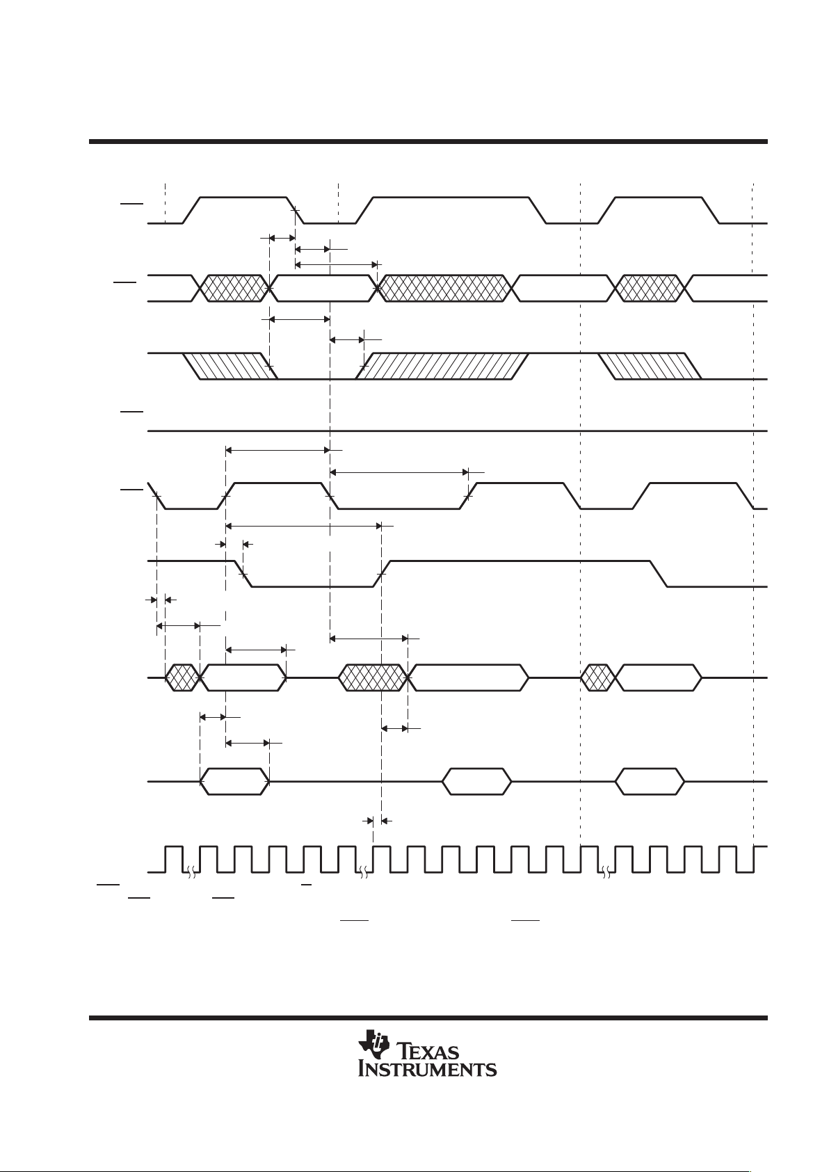
TMS320VC5409
FIXED-POINT DIGITAL SIGNAL PROCESSOR
SPRS082C – APRIL 1999 – REVISED MARCH 2000
69
POST OFFICE BOX 1443 • HOUSTON, TEXAS 77251–1443
HPI8 timing (continued)
Valid
t
su(HSL-DSL)
Valid
t
su(HBV-DSL)
t
su(HBV-DSL)
‡
HAS
HBIL
t
h(DSL-HBV)
t
h(DSL-HBV)
‡
t
d(DSH-HYH)
t
w(DSL)
t
d(DSL-HDV1)
t
v(HYH-HDV)
Valid Valid
Valid
t
d(COH-HYH)
Valid
t
w(DSH)
t
d(DSH-HYL)
t
h(DSH-HDV)R
t
h(DSH-HDV)W
Valid
t
su(HDV-DSH)
t
d(DSL-HDV2)
t
en(DSL-HD)
HCS
HDS
HRDY
HD READ
Valid
HD WRITE
CLKOUT
Second Byte First Byte Second Byte
HAD
†
†
HAD refers to HCNTL0, HCNTL1, and HR/W.
‡
When HAS
is not used (HAS always high)
Figure 37. Using HDS to Control Accesses (HCS Always Low)

TMS320VC5409
FIXED-POINT DIGITAL SIGNAL PROCESSOR
SPRS082C – APRIL 1999 – REVISED MARCH 2000
70
POST OFFICE BOX 1443 • HOUSTON, TEXAS 77251–1443
HPI8 timing (continued)
Second Byte
First Byte
Second Byte
t
d(HCS-HRDY)
HCS
HDS
HRDY
Figure 38. Using HCS to Control Accesses
CLKOUT
HRDY
t
d(COH–HYH)
Figure 39. HRDY Relative to CLKOUT
HINT
CLKOUT
t
d(COH-HTX)
Figure 40. HINT Timing
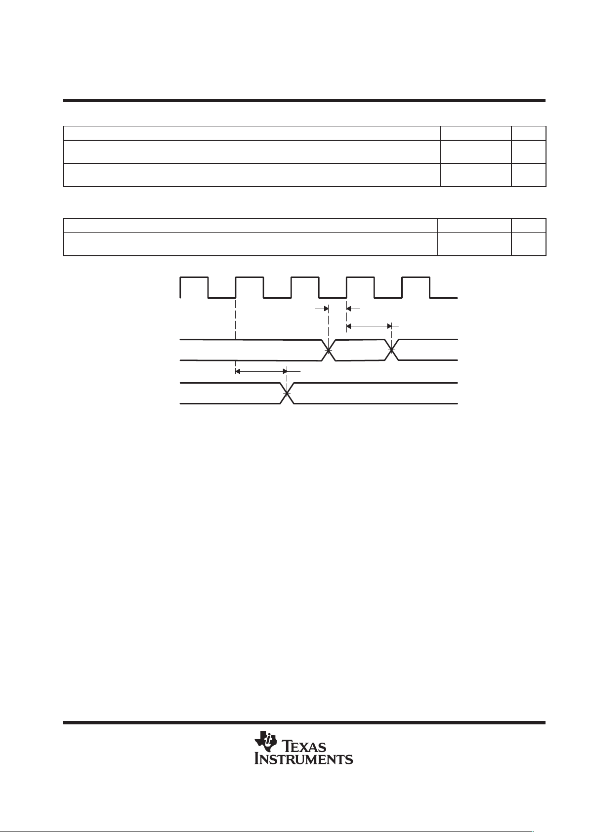
TMS320VC5409
FIXED-POINT DIGITAL SIGNAL PROCESSOR
SPRS082C – APRIL 1999 – REVISED MARCH 2000
71
POST OFFICE BOX 1443 • HOUSTON, TEXAS 77251–1443
timing requirements for GPIO (see Figure 41)
MIN MAX UNIT
t
su(GPIO-COH)
Setup time, GPIOx input valid before CLKOUT high, GPIOx configured as
general-purpose input.
7 ns
t
h(GPIO-COH)
Hold time, GPIOx input valid after CLKOUT high, GPIOx configured as general-purpose
input.
0 ns
switching characteristics for GPIO (see Figure 41)
PARAMETER MIN MAX UNIT
t
d(COH-GPIO)
Delay time, CLKOUT high to GPIOx output change. GPIOx configured as
general-purpose output.
0 6 ns
GPIOx Input Mode
†
CLKOUT
t
h(GPIO-COH)
GPIOx Output Mode
†
t
su(GPIO-COH)
t
d(COH-GPIO)
†
GPIOx refers to HD0, HD1, HD2, ...HD7, when the HD bus is configured for general-purpose input/output (I/O).
Figure 41. GPIOx† Timings
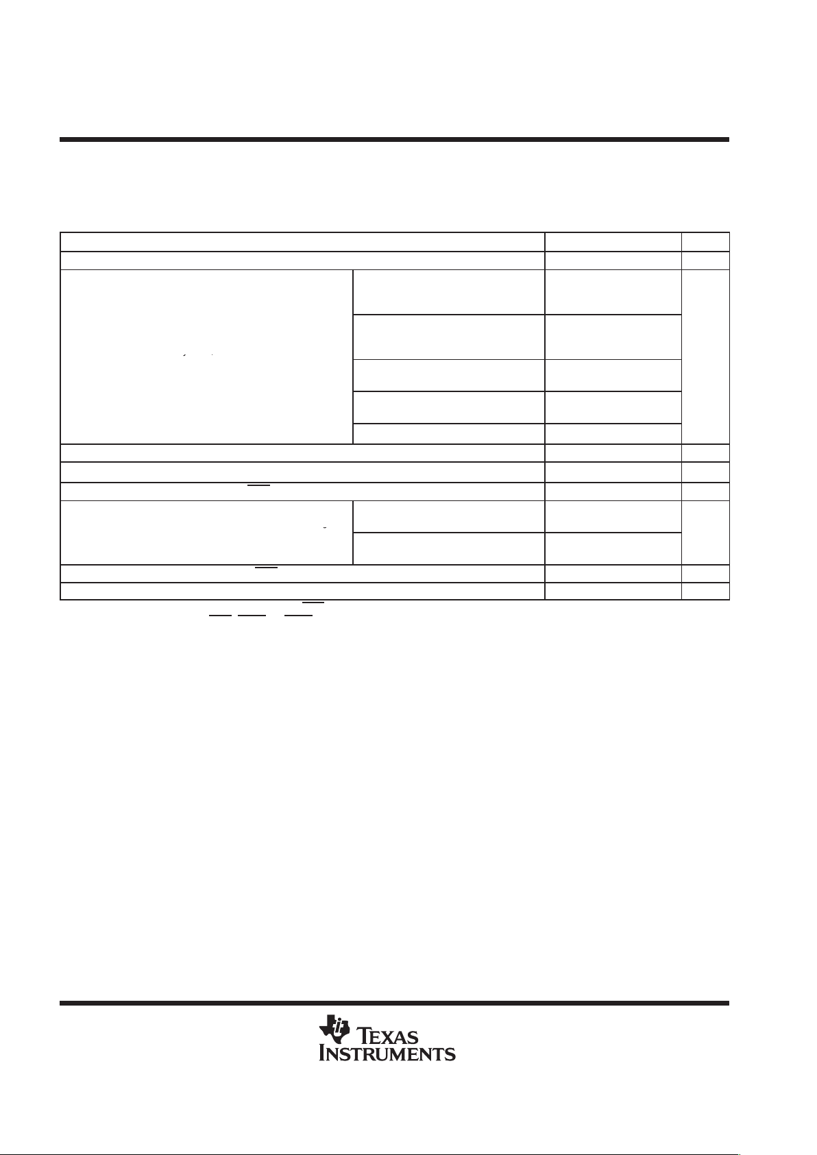
TMS320VC5409
FIXED-POINT DIGITAL SIGNAL PROCESSOR
SPRS082C – APRIL 1999 – REVISED MARCH 2000
72
POST OFFICE BOX 1443 • HOUSTON, TEXAS 77251–1443
HPI16 timing
switching characteristics over recommended operating conditions
†‡§
¶
[H = 0.5t
c(CO)
]
(see Figure 42 and Figure 43)
PARAMETER MIN MAX UNIT
t
en(DSL-HD)
Enable time, Dx driven from DS low 6 19 ns
Case 1a: Memory accesses when
DMAC is active in 16-bit mode and
t
w(DSH)
< 18H
18H+19 – t
w(DSH)
Delay time, DS low to Dx valid for an
Case 1b: Memory accesses when
DMAC is active in 16-bit mode and
t
w(DSH)
≥ 18H
19
t
d(DSL-HDV1)
y,
HPI read
Case 2a: Memory accesses when
DMAC is inactive and t
w(DSH)
< 10H
10H+19 – t
w(DSH)
ns
Case 2b: Memory accesses when
DMAC is inactive and t
w(DSH)
≥ 10H
19
Case 3: Register accesses 19
t
h(DSH-HDV)R
Hold time, Dx valid after DS rising edge, read
§
1 8 ns
tv
(HYH-HDV)
Valid time, Dx valid before HRDY rising edge
0 6 ns
t
d(DSH-HYL)
Delay time, DS or HCS high to HRDY low
‡
10 ns
Delay time, DS high to HRDY high
§
Case 1: Memory access when DMAC
is active in 16-bit mode
18H+10
t
d(DSH-HYH)
Delay time, DS high to HRDY high
§
(writes and autoincrement reads)
Case 2: Memory access when DMAC
is inactive
10H+10
ns
t
d(DSL-HYL)
Delay time, HDS or HCS low/high to HRDY low/high 10 ns
t
d(COH–HYH)
Delay time, CLKOUT high to HRDY high 2 ns
NOTE: The HRDY output is always high when the HCS input is high, regardless of DS timings.
†
DS refers to the logical OR of HCS
, HDS1, or HDS2.
‡
Dx refers to any of the DPI data bus pins (D0, D1, D2, etc.).
§
DMAC stands for direct memory access (DMA) controller. The HPI16 shares the internal DMA bus with the DMAC, thus HPI16 access times
are affected by DMAC activity.
¶
GPIO refers to the HD pins when they are configured as general-purpose input/outputs.

TMS320VC5409
FIXED-POINT DIGITAL SIGNAL PROCESSOR
SPRS082C – APRIL 1999 – REVISED MARCH 2000
73
POST OFFICE BOX 1443 • HOUSTON, TEXAS 77251–1443
HPI16 timing (continued)
timing requirements
†‡§
[H = 0.5t
c(CO)
] (see Note 1, Figure 42, and Figure 43)
MIN MAX UNIT
t
su(HBV-DSL)
Setup time, HAD valid before DS falling edge
†‡
5 ns
t
h(DSL-HBV)
Hold time, HAD valid after DS falling edge
†‡
5 ns
t
su(HAV-DSL)
Setup time, HAD valid before DS falling edge
†
–4H+3 ns
t
h(DSH-HAV)
Hold time, address valid after DS rising edge
†
1 ns
t
su(HDV-DSH)
Setup time, Dx valid before DS high (HPI write) 3 ns
t
h(DSH-HDV)W
Hold time, Dx valid after DS high (HPI write) 2 ns
t
w(DSL)
Pulse duration, DS low
‡
20 ns
t
w(DSH)
Pulse duration, DS high
‡
10 ns
Cycle time, DS rising edge to next DS rising
edge
‡
Nonmultiplexed mode (no increment)
with no DMA activity.
12H ns
t
c(DSH-DSH)
(Minimum timings represent WRITEs while
maximum timings represent READs)
Nonmultiplexed mode (no increment)
with 16-bit DMA activity.
20H ns
†
DS refers to the logical OR of HCS and HDS1 and HDS2.
‡
Dx refers to any of the HPI data bus pins (D0, D1, D2, etc.).
§
GPIO refers to the HD pins when they are configured as general-purpose input/outputs.

TMS320VC5409
FIXED-POINT DIGITAL SIGNAL PROCESSOR
SPRS082C – APRIL 1999 – REVISED MARCH 2000
74
POST OFFICE BOX 1443 • HOUSTON, TEXAS 77251–1443
HPI16 timing (continued)
t
d(DSL–HYH)
t
v(HYH–HDV)
t
h(DSH–HDV)R
t
d(DSL–HDV1)
t
en(DSL–HD)
t
h(DSH–HAV)
t
su(HAV–DSL)
t
h(DSL–HBV)
t
w(DSL)
t
su(HBV–DSL)
t
w(DSH)
t
c(DSH–DSH)
HRDY
HA[15:0]
HR/W
HDS
HCS
Data ValidData Valid
Valid AddressValid Address
(A[15:0])
D[15:0]
Figure 42. Nonmultiplexed Read Timings

TMS320VC5409
FIXED-POINT DIGITAL SIGNAL PROCESSOR
SPRS082C – APRIL 1999 – REVISED MARCH 2000
75
POST OFFICE BOX 1443 • HOUSTON, TEXAS 77251–1443
HPI16 timing (continued)
HRDY
D[15:0]
HA[15:0]
HR/W
HDS
HCS
Data ValidData Valid
t
h(DSH–HDV)W
t
su(HDV–DSH)
Valid AddressValid Address
t
h(DSH–HAV)
t
h(DSL–HBV)
t
w(DSL)
t
su(HBV–DSL)
t
w(DSH)
t
c(DSH–DSH)
t
su(HAV–DSH)
t
d(DSH–HYH)
t
d(DSL–HYL)
A[15:0]
Figure 43. Nonmultiplexed Write Timings
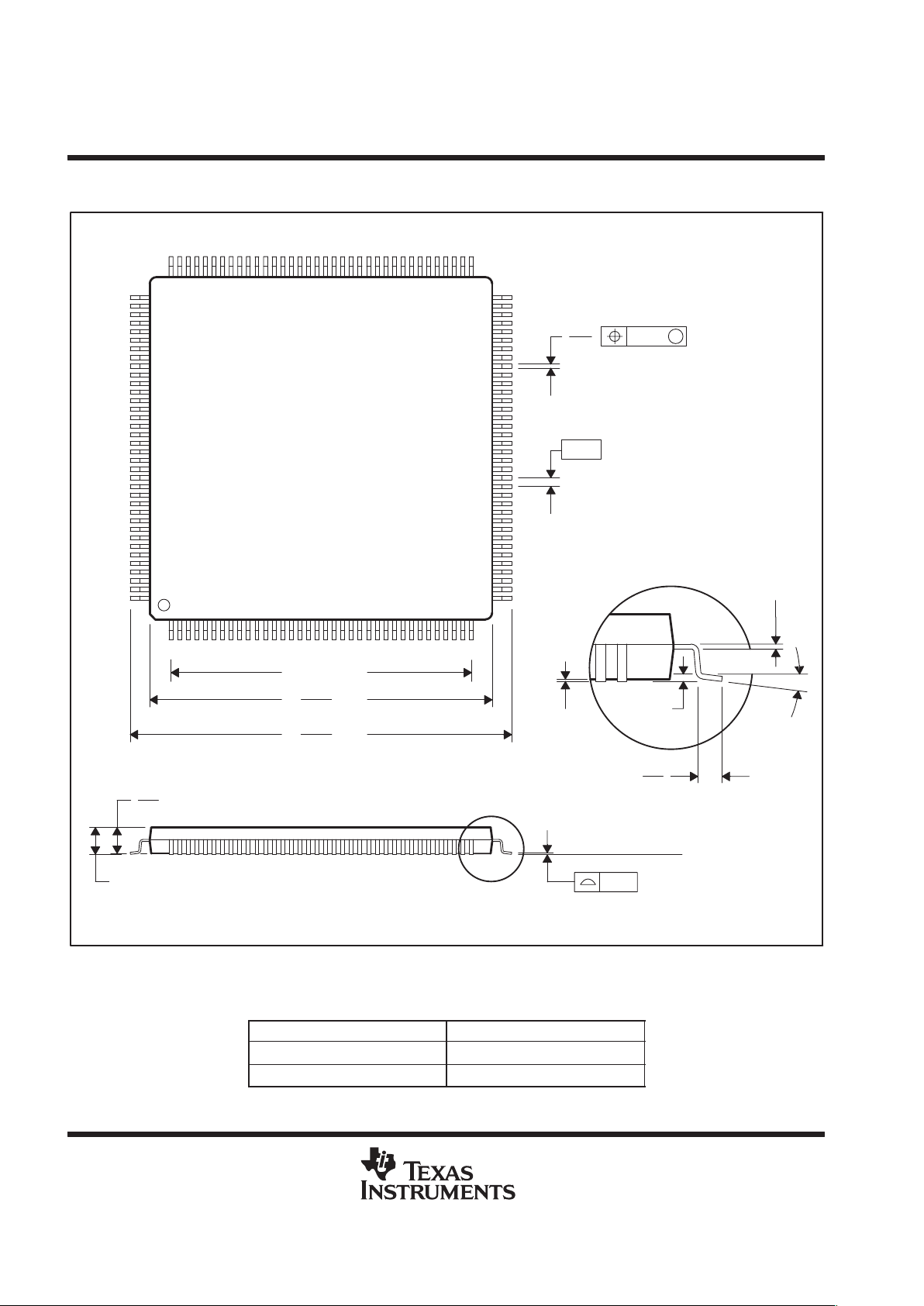
TMS320VC5409
FIXED-POINT DIGITAL SIGNAL PROCESSOR
SPRS082C – APRIL 1999 – REVISED MARCH 2000
76
POST OFFICE BOX 1443 • HOUSTON, TEXAS 77251–1443
MECHANICAL DATA
PGE (S-PQFP-G144) PLASTIC QUAD FLATPACK
4040147/C 10/96
0,27
72
0,17
37
73
0,13 NOM
0,25
0,75
0,45
0,05 MIN
36
Seating Plane
Gage Plane
108
109
144
SQ
SQ
22,20
21,80
1
19,80
17,50 TYP
20,20
1,35
1,45
1,60 MAX
M
0,08
0°–7°
0,08
0,50
NOTES: A. All linear dimensions are in millimeters.
B. This drawing is subject to change without notice.
C. Falls within JEDEC MS-026
Thermal Resistance Characteristics
PARAMETER
°C/W
R
ΘJA
56
R
ΘJC
5

TMS320VC5409
FIXED-POINT DIGITAL SIGNAL PROCESSOR
SPRS082C – APRIL 1999 – REVISED MARCH 2000
77
POST OFFICE BOX 1443 • HOUSTON, TEXAS 77251–1443
MECHANICAL DATA
GGU (S-PBGA-N144) PLASTIC BALL GRID ARRAY PACKAGE
0,80
0,10
M
0,08
0,80
9,60 TYP
12 1310 118967
N
M
K
L
J
H
42 3
F
E
C
B
D
A
1
G
5
Seating Plane
4073221/A 11/96
SQ
11,90
12,10
0,95
0,35
0,45
0,45
0,55
0,85
0,08
0,12
1,40 MAX
NOTES: A. All linear dimensions are in millimeters.
B. This drawing is subject to change without notice.
C. MicroStar BGA configuration
Thermal Resistance Characteristics
PARAMETER
°C/W
R
ΘJA
38
R
ΘJC
5
MicroStar BGA is a trademark of Texas Instruments Incorporated.

IMPORTANT NOTICE
T exas Instruments and its subsidiaries (TI) reserve the right to make changes to their products or to discontinue
any product or service without notice, and advise customers to obtain the latest version of relevant information
to verify, before placing orders, that information being relied on is current and complete. All products are sold
subject to the terms and conditions of sale supplied at the time of order acknowledgment, including those
pertaining to warranty, patent infringement, and limitation of liability.
TI warrants performance of its semiconductor products to the specifications applicable at the time of sale in
accordance with TI’s standard warranty. Testing and other quality control techniques are utilized to the extent
TI deems necessary to support this warranty. Specific testing of all parameters of each device is not necessarily
performed, except those mandated by government requirements.
Customers are responsible for their applications using TI components.
In order to minimize risks associated with the customer’s applications, adequate design and operating
safeguards must be provided by the customer to minimize inherent or procedural hazards.
TI assumes no liability for applications assistance or customer product design. TI does not warrant or represent
that any license, either express or implied, is granted under any patent right, copyright, mask work right, or other
intellectual property right of TI covering or relating to any combination, machine, or process in which such
semiconductor products or services might be or are used. TI’s publication of information regarding any third
party’s products or services does not constitute TI’s approval, warranty or endorsement thereof.
Copyright 2000, Texas Instruments Incorporated
 Loading...