

Page 1

现货库存、技术资料、百科信息、热点资讯,精彩尽在鼎好!
TMS320VC5407/TMS320VC5404
Fixed-Point Digital Signal
Processors
Data Manual
Literature Number: SPRS007D
November 2001 − Revised April 2004
PRODUCTION DATA information is current as of publication date.
Products conform to specifications per the terms of Texas Instruments
standard warranty. Production processing does not necessarily include
testing of all parameters.
Page 2

IMPORTANT NOTICE
Texas Instruments Incorporated and its subsidiaries (TI) reserve the right to make corrections, modifications,
enhancements, improvements, and other changes to its products and services at any time and to discontinue
any product or service without notice. Customers should obtain the latest relevant information before placing
orders and should verify that such information is current and complete. All products are sold subject to TI’s terms
and conditions of sale supplied at the time of order acknowledgment.
TI warrants performance of its hardware products to the specifications applicable at the time of sale in
accordance with TI’s standard warranty. Testing and other quality control techniques are used to the extent TI
deems necessary to support this warranty . Except where mandated by government requirements, testing of all
parameters of each product is not necessarily performed.
TI assumes no liability for applications assistance or customer product design. Customers are responsible for
their products and applications using TI components. To minimize the risks associated with customer products
and applications, customers should provide adequate design and operating safeguards.
TI does not warrant or represent that any license, either express or implied, is granted under any TI patent right,
copyright, mask work right, or other TI intellectual property right relating to any combination, machine, or process
in which TI products or services are used. Information published by TI regarding third-party products or services
does not constitute a license from TI to use such products or services or a warranty or endorsement thereof.
Use of such information may require a license from a third party under the patents or other intellectual property
of the third party, or a license from TI under the patents or other intellectual property of TI.
Reproduction of information in TI data books or data sheets is permissible only if reproduction is without
alteration and is accompanied by all associated warranties, conditions, limitations, and notices. Reproduction
of this information with alteration is an unfair and deceptive business practice. TI is not responsible or liable for
such altered documentation.
Resale of TI products or services with statements different from or beyond the parameters stated by TI for that
product or service voids all express and any implied warranties for the associated TI product or service and
is an unfair and deceptive business practice. TI is not responsible or liable for any such statements.
Following are URLs where you can obtain information on other Texas Instruments products and application
solutions:
Products Applications
Amplifiers amplifier.ti.com Audio www.ti.com/audio
Data Converters dataconverter.ti.com Automotive www.ti.com/automotive
DSP dsp.ti.com Broadband www.ti.com/broadband
Interface interface.ti.com Digital Control www.ti.com/digitalcontrol
Logic logic.ti.com Military www.ti.com/military
Power Mgmt power.ti.com Optical Networking www.ti.com/opticalnetwork
Microcontrollers microcontroller.ti.com Security www.ti.com/security
Telephony www.ti.com/telephony
Video & Imaging www.ti.com/video
Wireless www.ti.com/wireless
Mailing Address: Texas Instruments
Post Office Box 655303 Dallas, Texas 75265
Copyright 2004, Texas Instruments Incorporated
Page 3

Revision History
REVISION HISTORY
This data sheet revision history highlights the technical changes made to the SPRS007C device-specific data
sheet to make it an SPRS007D revision.
Scope: This document has been reviewed for technical accuracy; the technical content is up-to-date as of the
specified release date with the following changes.
PAGE(S)
NO.
21 Added “This pin must be tied directly to DVDD to enable HPI.” to the HPIENA description and “This pin must be tied directly to
38 Added the following to Section 3.9: “Since the Timer1 output is multiplexed externally with the HINT output, the HPI must be
42 Changed the parenthetical statement “(such as the McBSPs)” in Section 3.12. to read “(such as the McBSPs, but not the
48 Added the following footnote to Table 3−12: “Note that the UART DMA synchronization event is usable as a synchronization
59 Changed Figure 3−23, bit 15 from “Reserved” to “TOUT1”.
60 Added the following paragraph to Section 3.14.2: “Bit 15 of the GPIOCR is also used as the Timer1 output enable bit, TOUT1.
71 Changed the I
DV
to enable HPI16 mode.” to the HPI16 description in Table 2−2. Also deleted “Internally pulled low.” from the HPI16
DD
description.
disabled (HPIENA input pin = 0) if the Timer1 output is to be used. The Timer1 output also has a dedicated enable bit in the
General Purpose I/O Control Register (GPIOCR) located at data memory address 003Ch. If the external Timer1 output is to
be used, in addition to disabling the HPI, the TOUT1 bit in the GPIOCR must also be set to 1.”
UART)”
event only, and is not usable for transferring data to or from the UART. The DMA cannot be used to transfer data to or from
the UART.”
The TOUT1 bit enables or disables the Timer1 output on the HINT
available externally; if TOUT1 = 1, the Timer1 output is driven on the HINT
only available when the HPI is disabled (HPIENA input pin = 0).”
parameter from “60” to “42” in the Electrical Characteristics Over Recommended Operating Case
Temperature Range table.
DDC
ADDITIONS/CHANGES/DELETIONS
/TOUT1 pin. If TOUT1 = 0, the Timer1 output is not
/TOUT1 pin. Note also that the Timer1 output is
November 2001 − Revised April 2004 SPRS007D
3
Page 4

Revision History
4
November 2001 − Revised April 2004SPRS007D
Page 5

Contents
Contents
Section Page
1 TMS320VC5407/TMS320VC5404 Features 13. . . . . . . . . . . . . . . . . . . . . . . . . . . . . . . . . . . . . . . . . . . . . . . . .
2 Introduction 14. . . . . . . . . . . . . . . . . . . . . . . . . . . . . . . . . . . . . . . . . . . . . . . . . . . . . . . . . . . . . . . . . . . . . . . . . . . .
2.1 Description 14. . . . . . . . . . . . . . . . . . . . . . . . . . . . . . . . . . . . . . . . . . . . . . . . . . . . . . . . . . . . . . . . . . . . . .
2.2 Pin Assignments 14. . . . . . . . . . . . . . . . . . . . . . . . . . . . . . . . . . . . . . . . . . . . . . . . . . . . . . . . . . . . . . . . . .
2.2.1 Terminal Assignments for the GGU Package 15. . . . . . . . . . . . . . . . . . . . . . . . . . . . . . . .
2.2.2 Pin Assignments for the PGE Package 17. . . . . . . . . . . . . . . . . . . . . . . . . . . . . . . . . . . . .
2.3 Signal Descriptions 18. . . . . . . . . . . . . . . . . . . . . . . . . . . . . . . . . . . . . . . . . . . . . . . . . . . . . . . . . . . . . . .
3 Functional Overview 23. . . . . . . . . . . . . . . . . . . . . . . . . . . . . . . . . . . . . . . . . . . . . . . . . . . . . . . . . . . . . . . . . . . .
3.1 Memory 23. . . . . . . . . . . . . . . . . . . . . . . . . . . . . . . . . . . . . . . . . . . . . . . . . . . . . . . . . . . . . . . . . . . . . . . . .
3.1.1 Data Memory 23. . . . . . . . . . . . . . . . . . . . . . . . . . . . . . . . . . . . . . . . . . . . . . . . . . . . . . . . . . .
3.1.2 Program Memory 24. . . . . . . . . . . . . . . . . . . . . . . . . . . . . . . . . . . . . . . . . . . . . . . . . . . . . . .
3.1.3 Extended Program Memory 24. . . . . . . . . . . . . . . . . . . . . . . . . . . . . . . . . . . . . . . . . . . . . . .
3.2 On-Chip ROM With Bootloader 24. . . . . . . . . . . . . . . . . . . . . . . . . . . . . . . . . . . . . . . . . . . . . . . . . . . . .
3.3 On-Chip RAM 25. . . . . . . . . . . . . . . . . . . . . . . . . . . . . . . . . . . . . . . . . . . . . . . . . . . . . . . . . . . . . . . . . . . .
3.4 On-Chip Memory Security 25. . . . . . . . . . . . . . . . . . . . . . . . . . . . . . . . . . . . . . . . . . . . . . . . . . . . . . . . .
3.5 Memory Maps 26. . . . . . . . . . . . . . . . . . . . . . . . . . . . . . . . . . . . . . . . . . . . . . . . . . . . . . . . . . . . . . . . . . . .
3.5.1 5407 Memory Map 26. . . . . . . . . . . . . . . . . . . . . . . . . . . . . . . . . . . . . . . . . . . . . . . . . . . . . .
3.5.2 5404 Memory Map 27. . . . . . . . . . . . . . . . . . . . . . . . . . . . . . . . . . . . . . . . . . . . . . . . . . . . . .
3.5.3 Relocatable Interrupt Vector Table 28. . . . . . . . . . . . . . . . . . . . . . . . . . . . . . . . . . . . . . . . .
3.6 On-Chip Peripherals 30. . . . . . . . . . . . . . . . . . . . . . . . . . . . . . . . . . . . . . . . . . . . . . . . . . . . . . . . . . . . . .
3.6.1 Software-Programmable Wait-State Generator 30. . . . . . . . . . . . . . . . . . . . . . . . . . . . . .
3.6.2 Programmable Bank-Switching 32. . . . . . . . . . . . . . . . . . . . . . . . . . . . . . . . . . . . . . . . . . . .
3.6.3 Bus Holders 33. . . . . . . . . . . . . . . . . . . . . . . . . . . . . . . . . . . . . . . . . . . . . . . . . . . . . . . . . . . .
3.7 Parallel I/O Ports 33. . . . . . . . . . . . . . . . . . . . . . . . . . . . . . . . . . . . . . . . . . . . . . . . . . . . . . . . . . . . . . . . .
3.7.1 Enhanced 8-/16-Bit Host-Port Interface (HPI8/16) 33. . . . . . . . . . . . . . . . . . . . . . . . . . .
3.7.2 HPI Nonmultiplexed Mode 35. . . . . . . . . . . . . . . . . . . . . . . . . . . . . . . . . . . . . . . . . . . . . . . .
3.8 Multichannel Buffered Serial Ports (McBSPs) 36. . . . . . . . . . . . . . . . . . . . . . . . . . . . . . . . . . . . . . . . .
3.9 Hardware Timers 38. . . . . . . . . . . . . . . . . . . . . . . . . . . . . . . . . . . . . . . . . . . . . . . . . . . . . . . . . . . . . . . . .
3.10 Clock Generator 39. . . . . . . . . . . . . . . . . . . . . . . . . . . . . . . . . . . . . . . . . . . . . . . . . . . . . . . . . . . . . . . . . .
3.11 Enhanced External Parallel Interface (XIO2) 40. . . . . . . . . . . . . . . . . . . . . . . . . . . . . . . . . . . . . . . . . .
3.12 DMA Controller 42. . . . . . . . . . . . . . . . . . . . . . . . . . . . . . . . . . . . . . . . . . . . . . . . . . . . . . . . . . . . . . . . . . .
3.12.1 Features 43. . . . . . . . . . . . . . . . . . . . . . . . . . . . . . . . . . . . . . . . . . . . . . . . . . . . . . . . . . . . . . .
3.12.2 DMA External Access 43. . . . . . . . . . . . . . . . . . . . . . . . . . . . . . . . . . . . . . . . . . . . . . . . . . . .
3.12.3 DMA Memory Map 44. . . . . . . . . . . . . . . . . . . . . . . . . . . . . . . . . . . . . . . . . . . . . . . . . . . . . .
3.12.4 DMA Priority Level 46. . . . . . . . . . . . . . . . . . . . . . . . . . . . . . . . . . . . . . . . . . . . . . . . . . . . . .
3.12.5 DMA Source/Destination Address Modification 46. . . . . . . . . . . . . . . . . . . . . . . . . . . . . .
3.12.6 DMA in Autoinitialization Mode 46. . . . . . . . . . . . . . . . . . . . . . . . . . . . . . . . . . . . . . . . . . . .
3.12.7 DMA Transfer Counting 47. . . . . . . . . . . . . . . . . . . . . . . . . . . . . . . . . . . . . . . . . . . . . . . . . .
3.12.8 DMA Transfer in Doubleword Mode 47. . . . . . . . . . . . . . . . . . . . . . . . . . . . . . . . . . . . . . . .
3.12.9 DMA Channel Index Registers 47. . . . . . . . . . . . . . . . . . . . . . . . . . . . . . . . . . . . . . . . . . . .
3.12.10 DMA Interrupts 48. . . . . . . . . . . . . . . . . . . . . . . . . . . . . . . . . . . . . . . . . . . . . . . . . . . . . . . . .
3.12.11 DMA Controller Synchronization Events 48. . . . . . . . . . . . . . . . . . . . . . . . . . . . . . . . . . . .
November 2001 − Revised April 2004 SPRS007D
5
Page 6

Contents
Section Page
3.13 Universal Asynchronous Receiver/Transmitter (UART) 49. . . . . . . . . . . . . . . . . . . . . . . . . . . . . . . . .
3.13.1 UART Accessible Registers 52. . . . . . . . . . . . . . . . . . . . . . . . . . . . . . . . . . . . . . . . . . . . . .
3.13.2 FIFO Control Register (FCR) 53. . . . . . . . . . . . . . . . . . . . . . . . . . . . . . . . . . . . . . . . . . . . .
3.13.3 FIFO Interrupt Mode Operation 53. . . . . . . . . . . . . . . . . . . . . . . . . . . . . . . . . . . . . . . . . . .
3.13.4 FIFO Polled Mode Operation 54. . . . . . . . . . . . . . . . . . . . . . . . . . . . . . . . . . . . . . . . . . . . .
3.13.5 Interrupt Enable Register (IER) 54. . . . . . . . . . . . . . . . . . . . . . . . . . . . . . . . . . . . . . . . . . . .
3.13.6 Interrupt Identification Register (IIR) 54. . . . . . . . . . . . . . . . . . . . . . . . . . . . . . . . . . . . . . .
3.13.7 Line Control Register (LCR) 55. . . . . . . . . . . . . . . . . . . . . . . . . . . . . . . . . . . . . . . . . . . . . .
3.13.8 Line Status Register (LSR) 56. . . . . . . . . . . . . . . . . . . . . . . . . . . . . . . . . . . . . . . . . . . . . . .
3.13.9 Modem Control Register (MCR) 57. . . . . . . . . . . . . . . . . . . . . . . . . . . . . . . . . . . . . . . . . . .
3.13.10 Programmable Baud Generator 57. . . . . . . . . . . . . . . . . . . . . . . . . . . . . . . . . . . . . . . . . . .
3.14 General-Purpose I/O Pins 59. . . . . . . . . . . . . . . . . . . . . . . . . . . . . . . . . . . . . . . . . . . . . . . . . . . . . . . . . .
3.14.1 McBSP Pins as General-Purpose I/O 59. . . . . . . . . . . . . . . . . . . . . . . . . . . . . . . . . . . . . .
3.14.2 HPI Data Pins as General-Purpose I/O 59. . . . . . . . . . . . . . . . . . . . . . . . . . . . . . . . . . . . .
3.15 Device ID Register 60. . . . . . . . . . . . . . . . . . . . . . . . . . . . . . . . . . . . . . . . . . . . . . . . . . . . . . . . . . . . . . . .
3.16 Memory-Mapped Registers 61. . . . . . . . . . . . . . . . . . . . . . . . . . . . . . . . . . . . . . . . . . . . . . . . . . . . . . . .
3.17 McBSP Control Registers and Subaddresses 63. . . . . . . . . . . . . . . . . . . . . . . . . . . . . . . . . . . . . . . . .
3.18 DMA Subbank Addressed Registers 64. . . . . . . . . . . . . . . . . . . . . . . . . . . . . . . . . . . . . . . . . . . . . . . . .
3.19 Interrupts 66. . . . . . . . . . . . . . . . . . . . . . . . . . . . . . . . . . . . . . . . . . . . . . . . . . . . . . . . . . . . . . . . . . . . . . . .
3.19.1 IFR and IMR Registers 67. . . . . . . . . . . . . . . . . . . . . . . . . . . . . . . . . . . . . . . . . . . . . . . . . . .
4 Documentation Support 68. . . . . . . . . . . . . . . . . . . . . . . . . . . . . . . . . . . . . . . . . . . . . . . . . . . . . . . . . . . . . . . . .
4.1 Device and Development-Support Tool Nomenclature 69. . . . . . . . . . . . . . . . . . . . . . . . . . . . . . . . .
5 Electrical Specifications 70. . . . . . . . . . . . . . . . . . . . . . . . . . . . . . . . . . . . . . . . . . . . . . . . . . . . . . . . . . . . . . . .
5.1 Absolute Maximum Ratings 70. . . . . . . . . . . . . . . . . . . . . . . . . . . . . . . . . . . . . . . . . . . . . . . . . . . . . . . .
5.2 Recommended Operating Conditions 70. . . . . . . . . . . . . . . . . . . . . . . . . . . . . . . . . . . . . . . . . . . . . . . .
5.3 Electrical Characteristics Over Recommended Operating Case Temperature
Range (Unless Otherwise Noted) 71. . . . . . . . . . . . . . . . . . . . . . . . . . . . . . . . . . . . . . . . . . . . . . . . . . .
5.4 Package Thermal Resistance Characteristics 72. . . . . . . . . . . . . . . . . . . . . . . . . . . . . . . . . . . . . . . . .
5.5 Timing Parameter Symbology 72. . . . . . . . . . . . . . . . . . . . . . . . . . . . . . . . . . . . . . . . . . . . . . . . . . . . . .
5.6 Internal Oscillator With External Crystal 72. . . . . . . . . . . . . . . . . . . . . . . . . . . . . . . . . . . . . . . . . . . . . .
5.7 Clock Options 73. . . . . . . . . . . . . . . . . . . . . . . . . . . . . . . . . . . . . . . . . . . . . . . . . . . . . . . . . . . . . . . . . . . .
5.7.1 Divide-By-Two and Divide-By-Four Clock Options 73. . . . . . . . . . . . . . . . . . . . . . . . . . .
5.7.2 Multiply-By-N Clock Option (PLL Enabled) 75. . . . . . . . . . . . . . . . . . . . . . . . . . . . . . . . . .
5.8 Memory and Parallel I/O Interface Timing 76. . . . . . . . . . . . . . . . . . . . . . . . . . . . . . . . . . . . . . . . . . . .
5.8.1 Memory Read 76. . . . . . . . . . . . . . . . . . . . . . . . . . . . . . . . . . . . . . . . . . . . . . . . . . . . . . . . . .
5.8.2 Memory Write 79. . . . . . . . . . . . . . . . . . . . . . . . . . . . . . . . . . . . . . . . . . . . . . . . . . . . . . . . . .
5.8.3 I/O Read 81. . . . . . . . . . . . . . . . . . . . . . . . . . . . . . . . . . . . . . . . . . . . . . . . . . . . . . . . . . . . . . .
5.8.4 I/O Write 83. . . . . . . . . . . . . . . . . . . . . . . . . . . . . . . . . . . . . . . . . . . . . . . . . . . . . . . . . . . . . . .
5.9 Ready Timing for Externally Generated Wait States 84. . . . . . . . . . . . . . . . . . . . . . . . . . . . . . . . . . .
5.10 HOLD
and HOLDA Timings 87. . . . . . . . . . . . . . . . . . . . . . . . . . . . . . . . . . . . . . . . . . . . . . . . . . . . . . . .
5.11 Reset, BIO, Interrupt, and MP/MC Timings 88. . . . . . . . . . . . . . . . . . . . . . . . . . . . . . . . . . . . . . . . . . .
5.12 Instruction Acquisition (IAQ) and Interrupt Acknowledge (IACK) Timings 90. . . . . . . . . . . . . . . . .
5.13 External Flag (XF) and TOUT Timings 91. . . . . . . . . . . . . . . . . . . . . . . . . . . . . . . . . . . . . . . . . . . . . . .
6
November 2001 − Revised April 2004SPRS007D
Page 7

Contents
Section Page
5.14 Multichannel Buffered Serial Port (McBSP) Timing 92. . . . . . . . . . . . . . . . . . . . . . . . . . . . . . . . . . . .
5.14.1 McBSP Transmit and Receive Timings 92. . . . . . . . . . . . . . . . . . . . . . . . . . . . . . . . . . . . .
5.14.2 McBSP General-Purpose I/O Timing 95. . . . . . . . . . . . . . . . . . . . . . . . . . . . . . . . . . . . . . .
5.14.3 McBSP as SPI Master or Slave Timing 96. . . . . . . . . . . . . . . . . . . . . . . . . . . . . . . . . . . . .
5.15 Host-Port Interface Timing 100. . . . . . . . . . . . . . . . . . . . . . . . . . . . . . . . . . . . . . . . . . . . . . . . . . . . . . . . .
5.15.1 HPI8 Mode 100. . . . . . . . . . . . . . . . . . . . . . . . . . . . . . . . . . . . . . . . . . . . . . . . . . . . . . . . . . . . .
5.15.2 HPI16 Mode 104. . . . . . . . . . . . . . . . . . . . . . . . . . . . . . . . . . . . . . . . . . . . . . . . . . . . . . . . . . . .
5.16 UART Timing 107. . . . . . . . . . . . . . . . . . . . . . . . . . . . . . . . . . . . . . . . . . . . . . . . . . . . . . . . . . . . . . . . . . . . .
6 Mechanical Data 108. . . . . . . . . . . . . . . . . . . . . . . . . . . . . . . . . . . . . . . . . . . . . . . . . . . . . . . . . . . . . . . . . . . . . . . .
6.1 Ball Grid Array Mechanical Data 108. . . . . . . . . . . . . . . . . . . . . . . . . . . . . . . . . . . . . . . . . . . . . . . . . . . .
6.2 Low-Profile Quad Flatpack Mechanical Data 109. . . . . . . . . . . . . . . . . . . . . . . . . . . . . . . . . . . . . . . . . .
November 2001 − Revised April 2004 SPRS007D
7
Page 8

Figures
List of Figures
Figure Page
2−1 144-Ball GGU MicroStar BGA (Bottom View) 15. . . . . . . . . . . . . . . . . . . . . . . . . . . . . . . . . . . . . . . . . . . . .
2−2 144-Pin PGE Low-Profile Quad Flatpack (Top View) 17. . . . . . . . . . . . . . . . . . . . . . . . . . . . . . . . . . . . . .
3−1 TMS320VC5407/TMS320VC5404 Functional Block Diagram 23. . . . . . . . . . . . . . . . . . . . . . . . . . . . . . .
3−2 5407 Program and Data Memory Map 26. . . . . . . . . . . . . . . . . . . . . . . . . . . . . . . . . . . . . . . . . . . . . . . . . . .
3−3 5407 Extended Program Memory Map 26. . . . . . . . . . . . . . . . . . . . . . . . . . . . . . . . . . . . . . . . . . . . . . . . . .
3−4 5404 Program and Data Memory Map 27. . . . . . . . . . . . . . . . . . . . . . . . . . . . . . . . . . . . . . . . . . . . . . . . . . .
3−5 5404 Extended Program Memory Map 28. . . . . . . . . . . . . . . . . . . . . . . . . . . . . . . . . . . . . . . . . . . . . . . . . .
3−6 Processor Mode Status (PMST) Register 29. . . . . . . . . . . . . . . . . . . . . . . . . . . . . . . . . . . . . . . . . . . . . . . .
3−7 Software Wait-State Register (SWWSR) [Memory-Mapped Register (MMR) Address 0028h] 30. . .
3−8 Software Wait-State Control Register (SWCR) [MMR Address 002Bh] 31. . . . . . . . . . . . . . . . . . . . . . .
3−9 Bank-Switching Control Register (BSCR) [MMR Address 0029h] 32. . . . . . . . . . . . . . . . . . . . . . . . . . . .
3−10 Host-Port Interface — Nonmultiplexed Mode 35. . . . . . . . . . . . . . . . . . . . . . . . . . . . . . . . . . . . . . . . . . . . .
3−11 HPI Memory Map 35. . . . . . . . . . . . . . . . . . . . . . . . . . . . . . . . . . . . . . . . . . . . . . . . . . . . . . . . . . . . . . . . . . . .
3−12 Multichannel Control Register (MCR1) 37. . . . . . . . . . . . . . . . . . . . . . . . . . . . . . . . . . . . . . . . . . . . . . . . . .
3−13 Multichannel Control Register (MCR2) 37. . . . . . . . . . . . . . . . . . . . . . . . . . . . . . . . . . . . . . . . . . . . . . . . . .
3−14 Pin Control Register (PCR) 38. . . . . . . . . . . . . . . . . . . . . . . . . . . . . . . . . . . . . . . . . . . . . . . . . . . . . . . . . . . .
3−15 Nonconsecutive Memory Read and I/O Read Bus Sequence 40. . . . . . . . . . . . . . . . . . . . . . . . . . . . . . .
3−16 Consecutive Memory Read Bus Sequence (n = 3 reads) 41. . . . . . . . . . . . . . . . . . . . . . . . . . . . . . . . . . .
3−17 Memory Write and I/O Write Bus Sequence 42. . . . . . . . . . . . . . . . . . . . . . . . . . . . . . . . . . . . . . . . . . . . . .
3−18 DMA Transfer Mode Control Register (DMMCRn) 43. . . . . . . . . . . . . . . . . . . . . . . . . . . . . . . . . . . . . . . . .
3−19 On-Chip DMA Memory Map for Program Space (DLAXS = 0 and SLAXS = 0) 45. . . . . . . . . . . . . . . .
3−20 On-Chip DMA Memory Map for Data and IO Space (DLAXS = 0 and SLAXS = 0) 46. . . . . . . . . . . . .
3−21 DMPREC Register 47. . . . . . . . . . . . . . . . . . . . . . . . . . . . . . . . . . . . . . . . . . . . . . . . . . . . . . . . . . . . . . . . . . .
3−22 UART Functional Block Diagram 50. . . . . . . . . . . . . . . . . . . . . . . . . . . . . . . . . . . . . . . . . . . . . . . . . . . . . . .
3−23 General-Purpose I/O Control Register (GPIOCR) [MMR Address 003Ch] 59. . . . . . . . . . . . . . . . . . . .
3−24 General-Purpose I/O Status Register (GPIOSR) [MMR Address 003Dh] 60. . . . . . . . . . . . . . . . . . . . .
3−25 Device ID Register (CSIDR) [MMR Address 003Eh] 60. . . . . . . . . . . . . . . . . . . . . . . . . . . . . . . . . . . . . . .
3−26 IFR and IMR 67. . . . . . . . . . . . . . . . . . . . . . . . . . . . . . . . . . . . . . . . . . . . . . . . . . . . . . . . . . . . . . . . . . . . . . . . .
5−1 3.3-V Test Load Circuit 71. . . . . . . . . . . . . . . . . . . . . . . . . . . . . . . . . . . . . . . . . . . . . . . . . . . . . . . . . . . . . . . .
5−2 Internal Divide-by-Two Clock Option With External Crystal 73. . . . . . . . . . . . . . . . . . . . . . . . . . . . . . . . .
5−3 External Divide-by-Two Clock Timing 74. . . . . . . . . . . . . . . . . . . . . . . . . . . . . . . . . . . . . . . . . . . . . . . . . . . .
5−4 Multiply-by-One Clock Timing 75. . . . . . . . . . . . . . . . . . . . . . . . . . . . . . . . . . . . . . . . . . . . . . . . . . . . . . . . . .
5−5 Nonconsecutive Mode Memory Reads 77. . . . . . . . . . . . . . . . . . . . . . . . . . . . . . . . . . . . . . . . . . . . . . . . . .
5−6 Consecutive Mode Memory Reads 78. . . . . . . . . . . . . . . . . . . . . . . . . . . . . . . . . . . . . . . . . . . . . . . . . . . . .
5−7 Memory Write (MSTRB = 0) 80. . . . . . . . . . . . . . . . . . . . . . . . . . . . . . . . . . . . . . . . . . . . . . . . . . . . . . . . . . .
5−8 Parallel I/O Port Read (IOSTRB = 0) 82. . . . . . . . . . . . . . . . . . . . . . . . . . . . . . . . . . . . . . . . . . . . . . . . . . . .
5−9 Parallel I/O Port Write (IOSTRB = 0) 83. . . . . . . . . . . . . . . . . . . . . . . . . . . . . . . . . . . . . . . . . . . . . . . . . . . .
8
November 2001 − Revised April 2004SPRS007D
Page 9

Figures
Figure Page
5−10 Memory Read With Externally Generated Wait States 85. . . . . . . . . . . . . . . . . . . . . . . . . . . . . . . . . . . . .
5−11 Memory Write With Externally Generated Wait States 85. . . . . . . . . . . . . . . . . . . . . . . . . . . . . . . . . . . . .
5−12 I/O Read With Externally Generated Wait States 86. . . . . . . . . . . . . . . . . . . . . . . . . . . . . . . . . . . . . . . . .
5−13 I/O Write With Externally Generated Wait States 86. . . . . . . . . . . . . . . . . . . . . . . . . . . . . . . . . . . . . . . . .
5−14 HOLD
and HOLDA Timings (HM = 1) 87. . . . . . . . . . . . . . . . . . . . . . . . . . . . . . . . . . . . . . . . . . . . . . . . . . .
5−15 Reset and BIO Timings 88. . . . . . . . . . . . . . . . . . . . . . . . . . . . . . . . . . . . . . . . . . . . . . . . . . . . . . . . . . . . . . .
5−16 Interrupt Timing 89. . . . . . . . . . . . . . . . . . . . . . . . . . . . . . . . . . . . . . . . . . . . . . . . . . . . . . . . . . . . . . . . . . . . . .
5−17 MP/MC Timing 89. . . . . . . . . . . . . . . . . . . . . . . . . . . . . . . . . . . . . . . . . . . . . . . . . . . . . . . . . . . . . . . . . . . . . . .
5−18 Instruction Acquisition (IAQ) and Interrupt Acknowledge (IACK) Timings 90. . . . . . . . . . . . . . . . . . . . .
5−19 External Flag (XF) Timing 91. . . . . . . . . . . . . . . . . . . . . . . . . . . . . . . . . . . . . . . . . . . . . . . . . . . . . . . . . . . . .
5−20 TOUT Timing 91. . . . . . . . . . . . . . . . . . . . . . . . . . . . . . . . . . . . . . . . . . . . . . . . . . . . . . . . . . . . . . . . . . . . . . . .
5−21 McBSP Receive Timings 93. . . . . . . . . . . . . . . . . . . . . . . . . . . . . . . . . . . . . . . . . . . . . . . . . . . . . . . . . . . . . .
5−22 McBSP Transmit Timings 94. . . . . . . . . . . . . . . . . . . . . . . . . . . . . . . . . . . . . . . . . . . . . . . . . . . . . . . . . . . . . .
5−23 McBSP General-Purpose I/O Timings 95. . . . . . . . . . . . . . . . . . . . . . . . . . . . . . . . . . . . . . . . . . . . . . . . . . .
5−24 McBSP Timing as SPI Master or Slave: CLKSTP = 10b, CLKXP = 0 96. . . . . . . . . . . . . . . . . . . . . . . .
5−25 McBSP Timing as SPI Master or Slave: CLKSTP = 11b, CLKXP = 0 97. . . . . . . . . . . . . . . . . . . . . . . .
5−26 McBSP Timing as SPI Master or Slave: CLKSTP = 10b, CLKXP = 1 98. . . . . . . . . . . . . . . . . . . . . . . .
5−27 McBSP Timing as SPI Master or Slave: CLKSTP = 11b, CLKXP = 1 99. . . . . . . . . . . . . . . . . . . . . . . .
5−28 Using HDS to Control Accesses (HCS Always Low) 102. . . . . . . . . . . . . . . . . . . . . . . . . . . . . . . . . . . . . . .
5−29 Using HCS to Control Accesses 103. . . . . . . . . . . . . . . . . . . . . . . . . . . . . . . . . . . . . . . . . . . . . . . . . . . . . . . .
5−30 HINT Timing 103. . . . . . . . . . . . . . . . . . . . . . . . . . . . . . . . . . . . . . . . . . . . . . . . . . . . . . . . . . . . . . . . . . . . . . . . .
5−31 GPIOx Timings 103. . . . . . . . . . . . . . . . . . . . . . . . . . . . . . . . . . . . . . . . . . . . . . . . . . . . . . . . . . . . . . . . . . . . . .
5−32 Nonmultiplexed Read Timings 105. . . . . . . . . . . . . . . . . . . . . . . . . . . . . . . . . . . . . . . . . . . . . . . . . . . . . . . . . .
5−33 Nonmultiplexed Write Timings 106. . . . . . . . . . . . . . . . . . . . . . . . . . . . . . . . . . . . . . . . . . . . . . . . . . . . . . . . . .
5−34 HRDY Relative to CLKOUT 106. . . . . . . . . . . . . . . . . . . . . . . . . . . . . . . . . . . . . . . . . . . . . . . . . . . . . . . . . . . .
5−35 UART Timings 107. . . . . . . . . . . . . . . . . . . . . . . . . . . . . . . . . . . . . . . . . . . . . . . . . . . . . . . . . . . . . . . . . . . . . . .
6−1 TMS320VC5407/TMS320VC5404 144-Ball MicroStar BGA Plastic Ball Grid Array Package 108. . . .
6−2 TMS320VC5407/TMS320VC5404 144-Pin Low-Profile Quad Flatpack (PGE) 109. . . . . . . . . . . . . . . .
November 2001 − Revised April 2004 SPRS007D
9
Page 10

Tables
List of Tables
Table Page
2−1 Terminal Assignments for the 144-Pin BGA Package 16. . . . . . . . . . . . . . . . . . . . . . . . . . . . . . . . . . . . .
2−2 Signal Descriptions 18. . . . . . . . . . . . . . . . . . . . . . . . . . . . . . . . . . . . . . . . . . . . . . . . . . . . . . . . . . . . . . . . .
3−1 Standard On-Chip ROM Layout 25. . . . . . . . . . . . . . . . . . . . . . . . . . . . . . . . . . . . . . . . . . . . . . . . . . . . . . . .
3−2 Processor Mode Status (PMST) Register Bit Fields 29. . . . . . . . . . . . . . . . . . . . . . . . . . . . . . . . . . . . . .
3−3 Software Wait-State Register (SWWSR) Bit Fields 31. . . . . . . . . . . . . . . . . . . . . . . . . . . . . . . . . . . . . . .
3−4 Software Wait-State Control Register (SWCR) Bit Fields 31. . . . . . . . . . . . . . . . . . . . . . . . . . . . . . . . . .
3−5 Bank-Switching Control Register (BSCR) Fields 32. . . . . . . . . . . . . . . . . . . . . . . . . . . . . . . . . . . . . . . .
3−6 Bus Holder Control Bits 33. . . . . . . . . . . . . . . . . . . . . . . . . . . . . . . . . . . . . . . . . . . . . . . . . . . . . . . . . . . . . .
3−7 Sample Rate Input Clock Selection 38. . . . . . . . . . . . . . . . . . . . . . . . . . . . . . . . . . . . . . . . . . . . . . . . . . . . .
3−8 Clock Mode Settings at Reset 39. . . . . . . . . . . . . . . . . . . . . . . . . . . . . . . . . . . . . . . . . . . . . . . . . . . . . . . . .
3−9 DMD Section of the DMMCRn Register 44. . . . . . . . . . . . . . . . . . . . . . . . . . . . . . . . . . . . . . . . . . . . . . . . .
3−10 DMA Reload Register Selection 47. . . . . . . . . . . . . . . . . . . . . . . . . . . . . . . . . . . . . . . . . . . . . . . . . . . . . . .
3−11 DMA Interrupts 48. . . . . . . . . . . . . . . . . . . . . . . . . . . . . . . . . . . . . . . . . . . . . . . . . . . . . . . . . . . . . . . . . . . . . .
3−12 DMA Synchronization Events 48. . . . . . . . . . . . . . . . . . . . . . . . . . . . . . . . . . . . . . . . . . . . . . . . . . . . . . . . . .
3−13 DMA/CPU Channel Interrupt Selection 49. . . . . . . . . . . . . . . . . . . . . . . . . . . . . . . . . . . . . . . . . . . . . . . . .
3−14 UART Reset Functions 51. . . . . . . . . . . . . . . . . . . . . . . . . . . . . . . . . . . . . . . . . . . . . . . . . . . . . . . . . . . . . . .
3−15 Summary of Accessible Registers 52. . . . . . . . . . . . . . . . . . . . . . . . . . . . . . . . . . . . . . . . . . . . . . . . . . . . . .
3−16 Receiver FIFO Trigger Level 53. . . . . . . . . . . . . . . . . . . . . . . . . . . . . . . . . . . . . . . . . . . . . . . . . . . . . . . . . .
3−17 Interrupt Control Functions 55. . . . . . . . . . . . . . . . . . . . . . . . . . . . . . . . . . . . . . . . . . . . . . . . . . . . . . . . . . . .
3−18 Serial Character Word Length 55. . . . . . . . . . . . . . . . . . . . . . . . . . . . . . . . . . . . . . . . . . . . . . . . . . . . . . . . .
3−19 Number of Stop Bits Generated 56. . . . . . . . . . . . . . . . . . . . . . . . . . . . . . . . . . . . . . . . . . . . . . . . . . . . . . .
3−20 Baud Rates Using a 1.8432-MHz Clock 58. . . . . . . . . . . . . . . . . . . . . . . . . . . . . . . . . . . . . . . . . . . . . . . . .
3−21 Baud Rates Using a 3.072-MHz Clock 58. . . . . . . . . . . . . . . . . . . . . . . . . . . . . . . . . . . . . . . . . . . . . . . . . .
3−22 Device ID Register (CSIDR) Bit Functions 60. . . . . . . . . . . . . . . . . . . . . . . . . . . . . . . . . . . . . . . . . . . . .
3−23 CPU Memory-Mapped Registers 61. . . . . . . . . . . . . . . . . . . . . . . . . . . . . . . . . . . . . . . . . . . . . . . . . . . . .
3−24 Peripheral Memory-Mapped Registers for Each DSP Subsystem 62. . . . . . . . . . . . . . . . . . . . . . . . . .
3−25 McBSP Control Registers and Subaddresses 63. . . . . . . . . . . . . . . . . . . . . . . . . . . . . . . . . . . . . . . . . . . .
3−26 DMA Subbank Addressed Registers 64. . . . . . . . . . . . . . . . . . . . . . . . . . . . . . . . . . . . . . . . . . . . . . . . . .
3−27 Interrupt Locations and Priorities 66. . . . . . . . . . . . . . . . . . . . . . . . . . . . . . . . . . . . . . . . . . . . . . . . . . . . . . .
5−1 Thermal Resistance Characteristics 72. . . . . . . . . . . . . . . . . . . . . . . . . . . . . . . . . . . . . . . . . . . . . . . . . . . .
5−2 Input Clock Frequency Characteristics 72. . . . . . . . . . . . . . . . . . . . . . . . . . . . . . . . . . . . . . . . . . . . . . . . . .
5−3 Clock Mode Pin Settings for the Divide-By-2 and By Divide-by-4 Clock Options 73. . . . . . . . . . . . . .
5−4 Divide-By-2 and Divide-by-4 Clock Options Timing Requirements 74. . . . . . . . . . . . . . . . . . . . . . . . . .
5−5 Divide-By-2 and Divide-by-4 Clock Options Switching Characteristics 74. . . . . . . . . . . . . . . . . . . . . . .
5−6 Multiply-By-N Clock Option Timing Requirements 75. . . . . . . . . . . . . . . . . . . . . . . . . . . . . . . . . . . . . . . .
5−7 Multiply-By-N Clock Option Switching Characteristics 75. . . . . . . . . . . . . . . . . . . . . . . . . . . . . . . . . . . . .
5−8 Memory Read Timing Requirements 76. . . . . . . . . . . . . . . . . . . . . . . . . . . . . . . . . . . . . . . . . . . . . . . . . . .
5−9 Memory Read Switching Characteristics 76. . . . . . . . . . . . . . . . . . . . . . . . . . . . . . . . . . . . . . . . . . . . . . . .
5−10 Memory Write Switching Characteristics 79. . . . . . . . . . . . . . . . . . . . . . . . . . . . . . . . . . . . . . . . . . . . . . . .
5−11 I/O Read Timing Requirements 81. . . . . . . . . . . . . . . . . . . . . . . . . . . . . . . . . . . . . . . . . . . . . . . . . . . . . . . .
5−12 I/O Read Switching Characteristics 81. . . . . . . . . . . . . . . . . . . . . . . . . . . . . . . . . . . . . . . . . . . . . . . . . . . . .
5−13 I/O Write Switching Characteristics 83. . . . . . . . . . . . . . . . . . . . . . . . . . . . . . . . . . . . . . . . . . . . . . . . . . . . .
10
November 2001 − Revised April 2004SPRS007D
Page 11

Tables
Table Page
5−14 Ready Timing Requirements for Externally Generated Wait States 84. . . . . . . . . . . . . . . . . . . . . . . . .
5−15 Ready Switching Characteristics for Externally Generated Wait States 84. . . . . . . . . . . . . . . . . . . . . .
5−16 HOLD
and HOLDA Timing Requirements 87. . . . . . . . . . . . . . . . . . . . . . . . . . . . . . . . . . . . . . . . . . . . . . .
5−17 HOLD and HOLDA Switching Characteristics 87. . . . . . . . . . . . . . . . . . . . . . . . . . . . . . . . . . . . . . . . . . . .
5−18 Reset, BIO, Interrupt, and MP/MC Timing Requirements 88. . . . . . . . . . . . . . . . . . . . . . . . . . . . . . . . . .
5−19 Instruction Acquisition (IAQ) and Interrupt Acknowledge (IACK) Switching Characteristics 90. . . . .
5−20 External Flag (XF) and TOUT Switching Characteristics 91. . . . . . . . . . . . . . . . . . . . . . . . . . . . . . . . . .
5−21 McBSP Transmit and Receive Timing Requirements 92. . . . . . . . . . . . . . . . . . . . . . . . . . . . . . . . . . . . .
5−22 McBSP Transmit and Receive Switching Characteristics 93. . . . . . . . . . . . . . . . . . . . . . . . . . . . . . . . . .
5−23 McBSP General-Purpose I/O Timing Requirements 95. . . . . . . . . . . . . . . . . . . . . . . . . . . . . . . . . . . . . .
5−24 McBSP General-Purpose I/O Switching Characteristics 95. . . . . . . . . . . . . . . . . . . . . . . . . . . . . . . . . . .
5−25 McBSP as SPI Master or Slave Timing Requirements (CLKSTP = 10b, CLKXP = 0) 96. . . . . . . . . .
5−26 McBSP as SPI Master or Slave Switching Characteristics (CLKSTP = 10b, CLKXP = 0) 96. . . . . .
5−27 McBSP as SPI Master or Slave Timing Requirements (CLKSTP = 11b, CLKXP = 0) 97. . . . . . . . . .
5−28 McBSP as SPI Master or Slave Switching Characteristics (CLKSTP = 11b, CLKXP = 0) 97. . . . . . .
5−29 McBSP as SPI Master or Slave Timing Requirements (CLKSTP = 10b, CLKXP = 1) 98. . . . . . . . . .
5−30 McBSP as SPI Master or Slave Switching Characteristics (CLKSTP = 10b, CLKXP = 1) 98. . . . . .
5−31 McBSP as SPI Master or Slave Timing Requirements (CLKSTP = 11b, CLKXP = 1) 99. . . . . . . . . .
5−32 McBSP as SPI Master or Slave Switching Characteristics (CLKSTP = 11b, CLKXP = 1) 99. . . . . . .
5−33 HPI8 Mode Timing Requirements 100. . . . . . . . . . . . . . . . . . . . . . . . . . . . . . . . . . . . . . . . . . . . . . . . . . . . . .
5−34 HPI8 Mode Switching Characteristics 101. . . . . . . . . . . . . . . . . . . . . . . . . . . . . . . . . . . . . . . . . . . . . . . . .
5−35 HPI16 Mode Timing Requirements 104. . . . . . . . . . . . . . . . . . . . . . . . . . . . . . . . . . . . . . . . . . . . . . . . . . . . .
5−36 HPI16 Mode Switching Characteristics 105. . . . . . . . . . . . . . . . . . . . . . . . . . . . . . . . . . . . . . . . . . . . . . . . .
5−37 UART Timing Requirements 107. . . . . . . . . . . . . . . . . . . . . . . . . . . . . . . . . . . . . . . . . . . . . . . . . . . . . . . . . . .
5−38 UART Switching Characteristics 107. . . . . . . . . . . . . . . . . . . . . . . . . . . . . . . . . . . . . . . . . . . . . . . . . . . . . . .
November 2001 − Revised April 2004 SPRS007D
11
Page 12

Tables
12
November 2001 − Revised April 2004SPRS007D
Page 13

1 TMS320VC5407/TMS320VC5404 Features
Features
D Advanced Multibus Architecture With Three
Separate 16-Bit Data Memory Buses and
One Program Memory Bus
D 40-Bit Arithmetic Logic Unit (ALU)
Including a 40-Bit Barrel Shifter and Two
Independent 40-Bit Accumulators
D 17- × 17-Bit Parallel Multiplier Coupled to a
40-Bit Dedicated Adder for Non-Pipelined
Single-Cycle Multiply/Accumulate (MAC)
Operation
D Compare, Select, and Store Unit (CSSU) for
the Add/Compare Selection of the Viterbi
Operator
D Exponent Encoder to Compute an
Exponent Value of a 40-Bit Accumulator
Value in a Single Cycle
D Two Address Generators With Eight
Auxiliary Registers and Two Auxiliary
Register Arithmetic Units (ARAUs)
D Data Bus With a Bus Holder Feature
D Extended Addressing Mode for 8M × 16-Bit
Maximum Addressable External Program
Space
D On-Chip ROM
− 128K × 16-Bit (5407) Configured for
Program Memory
− 64K × 16-Bit (5404) Configured for
Program Memory
D On-Chip RAM
− 40K x 16-Bit (5407) Composed of
Five Blocks of 8K × 16-Bit On-Chip
Dual-Access Program/Data RAM
− 16K x 16-Bit (5404) Composed of
Two Blocks of 8K × 16-Bit On-Chip
Dual-Access Program/Data RAM
D Enhanced External Parallel Interface (XIO2)
D Single-Instruction-Repeat and
Block-Repeat Operations for Program Code
D Block-Memory-Move Instructions for Better
Program and Data Management
D Instructions With a 32-Bit Long Word
Operand
D Instructions With Two- or Three-Operand
Reads
D Arithmetic Instructions With Parallel Store
and Parallel Load
D Conditional Store Instructions
D Fast Return From Interrupt
D On-Chip Peripherals
− Software-Programmable Wait-State
Generator and Programmable
Bank-Switching
− On-Chip Programmable Phase-Locked
Loop (PLL) Clock Generator With
External Clock Source
− Two 16-Bit Timers
− Six-Channel Direct Memory Access
(DMA) Controller
− Three Multichannel Buffered Serial Ports
(McBSPs)
− 8/16-Bit Enhanced Parallel Host-Port
Interface (HPI8/16)
− Universal Asynchronous Receiver/
Transmitter (UART) With Integrated Baud
Rate Generator
D Power Consumption Control With IDLE1,
IDLE2, and IDLE3 Instructions With
Power-Down Modes
D CLKOUT Off Control to Disable CLKOUT
D On-Chip Scan-Based Emulation Logic,
IEEE Std 1149.1
Logic
†
(JTAG) Boundary Scan
D 144-Pin Ball Grid Array (BGA)
(GGU Suffix)
D 144-Pin Low-Profile Quad Flatpack (LQFP)
(PGE Suffix)
D 8.33-ns Single-Cycle Fixed-Point
Instruction Execution Time (120 MIPS)
D 3.3-V I/O Supply Voltage
D 1.5-V Core Supply Voltage
†
IEEE Standard 1149.1-1990 Standard-Test-Access Port and Boundary Scan Architecture.
All trademarks are the property of their respective owners.
November 2001 − Revised April 2004 SPRS007D
13
Page 14

Introduction
2 Introduction
This data manual discusses features and specifications of the TMS320VC5407 and TMS320VC5404
(hereafter referred to as the 5407/5404 unless otherwise specified) digital signal processors (DSPs). The 5407
and 5404 are essentially the same device except for differences in their memory maps.
This section lists the pin assignments and describes the function of each pin. This data manual also provides
a detailed description section, electrical specifications, parameter measurement information, and mechanical
data about the available packaging.
NOTE: This data manual is designed to be used in conjunction with the TMS320C54x DSP Functional
Overview (literature number SPRU307).
2.1 Description
The 5407/5404 are based on an advanced modified Harvard architecture that has one program memory bus
and three data memory buses. These processors provide an arithmetic logic unit (ALU) with a high degree
of parallelism, application-specific hardware logic, on-chip memory, and additional on-chip peripherals. The
basis of the operational flexibility and speed of these DSPs is a highly specialized instruction set.
Separate program and data spaces allow simultaneous access to program instructions and data, providing
a high degree of parallelism. Two read operations and one write operation can be performed in a single cycle.
Instructions with parallel store and application-specific instructions can fully utilize this architecture. In
addition, data can be transferred between data and program spaces. Such parallelism supports a powerful
set of arithmetic, logic, and bit-manipulation operations that can all be performed in a single machine cycle.
These DSPs also include the control mechanisms to manage interrupts, repeated operations, and function
calls.
2.2 Pin Assignments
Figure 2−1 illustrates the ball locations for the 144-pin ball grid array (BGA) package and is used in conjunction
with Table 2−1 to locate signal names and ball grid numbers. Figure 2−2 provides the pin assignments for the
144-pin low-profile quad flatpack (LQFP) package.
TMS320C54x is a trademark of Texas Instruments.
14
November 2001 − Revised April 2004SPRS007D
Page 15

2.2.1 Terminal Assignments for the GGU Package
Figure 2−1. 144-Ball GGU MicroStar BGA (Bottom View)
Introduction
12
3456781012 1113 9
A
B
C
D
E
F
G
H
J
K
L
M
N
Table 2−1 lists each signal name and BGA ball number for the 144-pin TMS320VC5407/
TMS320VC5404GGU package. Table 2−2 lists each terminal name, terminal function, and operating modes
for the TMS320VC5407/TMS320VC5404.
MicroStar BGA is a trademark of Texas Instruments.
November 2001 − Revised April 2004 SPRS007D
15
Page 16
Introduction
†
SIGNAL
QUADRANT 4
SIGNAL
QUADRANT 1
V
SS
Table 2−1. Terminal Assignments for the 144-Pin BGA Package
SIGNAL
BGA BALL #
QUADRANT 2
BGA BALL #
A1 BCLKRX2 N13 V
SIGNAL
QUADRANT 3
SS
BGA BALL #
N1 A19 A13
A22 B1 BDX2 M13 TX N2 A20 A12
V
DV
SS
DD
C2 DV
C1 V
SS
DD
L12 HCNTL0 M3 V
L13 V
SS
N3 DV
SS
DD
A10 D4 CLKMD1 K10 BCLKR0 K4 D6 D10
HD7 D3 CLKMD2 K11 BCLKR1 L4 D7 C10
A11 D2 CLKMD3 K12 BFSR0 M4 D8 B10
A12 D1 HPI16 K13 BFSR1 N4 D9 A10
A13 E4 HD2 J10 BDR0 K5 D10 D9
A14 E3 TOUT J11 HCNTL1 L5 D11 C9
A15 E2 EMU0 J12 BDR1 M5 D12 B9
CV
DD
E1 EMU1/OFF J13 BCLKX0 N5 HD4 A9
HAS F4 TDO H10 BCLKX1 K6 D13 D8
V
SS
V
SS
CV
DD
HCS G2 TMS G12 BFSX0 M7 CV
HR/W G1 V
READY G3 CV
PS G4 HPIENA G10 DV
DS H1 V
IS H2 CLKOUT F12 HD0 M8 DV
F3 TDI H11 V
SS
L6 D14 C8
F2 TRST H12 HINT/TOUT1 M6 D15 B8
F1 TCK H13 CVDD N6 HD5 A8
DD
SS
DD
SS
G13 BFSX1 N7 V
SS
G11 HRDY L7 HDS1 C7
K7 V
SS
N8 HDS2 A6
DD
F13 V
DD
SS
R/W H3 HD3 F11 BDX0 L8 A0 C6
MSTRB H4 X1 F10 BDX1 K8 A1 D6
IOSTRB J1 X2/CLKIN E13 IACK N9 A2 A5
MSC J2 RS E12 HBIL M9 A3 B5
XF J3 D0 E11 NMI L9 HD6 C5
HOLDA J4 D1 E10 INT0 K9 A4 D5
IAQ K1 D2 D13 INT1 N10 A5 A4
HOLD K2 D3 D12 INT2 M10 A6 B4
BIO K3 D4 D11 INT3 L10 A7 C4
MP/MC L1 D5 C13 CV
DV
DD
V
SS
L2 A16 C12 HD1 M11 A9 B3
L3 V
SS
C11 V
DD
SS
N11 A8 A3
L11 CV
DD
BDR2 M1 A17 B13 RX N12 A21 A2
BFSRX2 M2 A18 B12 V
SS
M12 V
SS
BGA BALL #
B11
A11
B7
A7
D7
B6
C3
B2
†
DVDD is the power supply for the I/O pins while CVDD is the power supply for the core CPU. VSS is the ground for both the I/O pins and the
core CPU.
16
November 2001 − Revised April 2004SPRS007D
Page 17
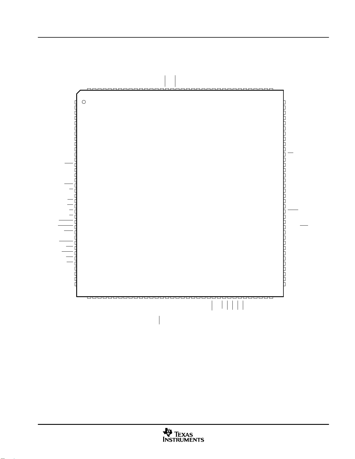
2.2.2 Pin Assignments for the PGE Package
The TMS320VC5407/TMS320VC5404PGE 144-pin low-profile quad flatpack (LQFP) pin assignments are
shown in Figure 2−2.
Introduction
V
A22
V
DV
DD
A10
HD7
A11
A12
A13
A14
A15
CV
DD
HAS
V
V
CV
DD
HCS
HR/W
READY
PS
DS
R/W
MSTRB
IOSTRB
MSC
XF
HOLDA
IAQ
HOLD
BIO
MP/MC
DV
DD
V
BDR2
BFSRX2
DD
SS
A9
A21
V
144CV143
142
141A8140A7139A6138A5137A4136
1
SS
2
3
SS
4
5
6
7
8
9
10
11
12
13
14
SS
15
SS
16
17
18
19
20
21
22
IS
23
24
25
26
27
28
29
30
31
32
33
34
SS
35
36
373839404142434445464748495051525354555657585960616263646566676869
HD6
135A3134A2133A1132A0131DV130
DD
HDS2SSV
129
128
SS
V
HDS1
127
126
DD
CV
125
HD5
124
D15
123
D14
122
D13
121
HD4
120
D12
119
D11
118
D10
117D9116D8115D7114D6113
DD
DV
112
SS
V
A20
111
110
707172
A19
109
108
107
106
105
104
103
102
101
100
99
98
97
96
95
94
93
92
91
90
89
88
87
86
85
84
83
82
81
80
79
78
77
76
75
74
73
A18
A17
V
SS
A16
D5
D4
D3
D2
D1
D0
RS
X2/CLKIN
X1
HD3
CLKOUT
V
SS
HPIENA
CV
DD
V
SS
TMS
TCK
TRST
TDI
TDO
EMU1/OFF
EMU0
TOUT
HD2
HPI16
CLKMD3
CLKMD2
CLKMD1
V
SS
DV
DD
BDX2
BCLKRX2
V
SS
TX
V
HCNTL0SSBCLKR0
BFSR0
BCLKR1
BDR0
BFSR1
BDR1
BCLKX0
HCNTL1
SS
V
BCLKX1
DD
CV
BFSX0
BFSX1
DD
HRDY
DV
SS
HD0
V
BDX0
IACK
BDX1
HBIL
NMI
INT0
INT1
INT2
INT3
DD
CV
HD1
SS
SS
RX
V
V
HINT/TOUT1
NOTE A: DVDD is the power supply for the I/O pins while CVDD is the power supply for the core CPU. VSS is the ground for both the I/O pins and
the core CPU.
Figure 2−2. 144-Pin PGE Low-Profile Quad Flatpack (Top View)
November 2001 − Revised April 2004 SPRS007D
17
Page 18
Introduction
2.3 Signal Descriptions
Table 2−2 lists each signal, function, and operating mode(s) grouped by function. See Section 2.2 for exact
pin locations based on package type.
Table 2−2. Signal Descriptions
TERMINAL
NAME
A22 (MSB)
A21
A20
A19
A18
A17
A16
A15
A14
A13
A12
A11
A10
A9
A8
A7
A6
A5
A4
A3
A2
A1
A0 (LSB)
D15 (MSB)
D14
D13
D12
D11
D10
D9
D8
D7
D6
D5
D4
D3
D2
D1
D0 (LSB)
IACK O/Z Interrupt acknowledge signal. IACK Indicates receipt of an interrupt and that the program counter is fetching
INT0
INT1
INT2
INT3
NMI I Nonmaskable interrupt. NMI is an external interrupt that cannot be masked by way of the INTM or the IMR.
†
I = Input, O = Output, Z = High-impedance, S = Supply
†
I/O
EXTERNAL MEMORY INTERFACE PINS
O/Z Parallel address bus A22 (MSB) through A0 (LSB). The lower sixteen address pins—A0 to A15—are
I/O/Z D15 (MSB)
multiplexed to address all external memory (program, data) or I/O, while the upper seven address
pins—A22 to A16—are only used to address external program space. These pins are placed in the
high-impedance state when the hold mode is enabled, or when OFF
A15 (MSB)
A14
A13
A12
A11
A10
A9
A8
A7
A6
A5
A4
A3
A2
A1
A0 (LSB)
D14
D13
D12
D11
D10
D9
D8
D7
D6
D5
D4
D3
D2
D1
D0 (LSB)
the interrupt vector location designated by A15–0. IACK
is low.
I External user interrupt inputs. INT0−3 are prioritized and maskable via the interrupt mask register and
interrupt mode bit. The status of these pins can be polled by way of the interrupt flag register.
When NMI
I These pins can be used to address internal memory via the HPI when the HPI16 pin
is high.
I/O Parallel data bus D15 (MSB) through D0 (LSB). The sixteen data pins, D0 to D15,
are multiplexed to transfer data between the core CPU and external data/program
memory, I/O devices, or HPI in 16-bit mode. The data bus is placed in the
high-impedance state when not outputting or when RS
data bus also goes into the high-impedance state when OFF
The data bus includes bus holders to reduce the static power dissipation caused by
floating, unused pins. The bus holders also eliminate the need for external bias
resistors on unused pins. When the data bus is not being driven by the DSP, the bus
holders keep the pins at the logic level that was most recently driven. The data bus
holders of the DSP are disabled at reset, and can be enabled/disabled via the BH bit
of the BSCR.
INITIALIZATION, INTERRUPT, AND RESET PINS
is activated, the processor traps to the appropriate vector location.
DESCRIPTION
is low.
or HOLD is asserted. The
is low.
also goes into the high-impedance state when OFF
18
November 2001 − Revised April 2004SPRS007D
Page 19
Introduction
Table 2−2. Signal Descriptions (Continued)
TERMINAL
NAME
RS I Reset input. RS causes the DSP to terminate execution and causes a re-initialization of the CPU and
MP/MC I Microprocessor/microcomputer mode select pin. If active low at reset, microcomputer mode is selected, and
BIO I Branch control input. A branch can be conditionally executed when BIO is active. If low, the processor
XF O/Z External flag output (latched software-programmable signal). XF is set high by the SSBX XF instruction, set
DS
PS
IS
MSTRB O/Z Memory strobe signal. MSTRB is always high unless low-level asserted to indicate an external bus access
READY I Data ready input. READY indicates that an external device is prepared for a bus transaction to be
R/W O/Z Read/write signal. R/W indicates transfer direction during communication to an external device. Normally in
IOSTRB O/Z I/O strobe signal. IOSTRB is always high unless low level asserted to indicate an external bus access to an
HOLD I Hold input. HOLD is asserted to request control of the address, data, and control lines. When
HOLDA O/Z Hold acknowledge signal. HOLDA indicates that the DSP is in a hold state and that the address, data, and
MSC O/Z Microstate complete. MSC indicates completion of all software wait states. When two or more software wait
IAQ O/Z Instruction acquisition signal. IAQ is asserted (active low) when there is an instruction address on the
†
I = Input, O = Output, Z = High-impedance, S = Supply
†
INITIALIZATION, INTERRUPT, AND RESET PINS (CONTINUED)
peripherals. When RS
affects various registers and status bits.
RS
the internal program ROM is mapped into the upper 16K words of program memory space. If the pin is
driven high during reset, microprocessor mode is selected, and the on-chip ROM is removed from program
space. This pin is only sampled at reset, and the MP/MC
that is selected at reset.
MULTIPROCESSING AND GENERAL PURPOSE PINS
executes the conditional instruction. The BIO
for XC instruction, and all other instructions sample BIO
low by RSBX XF instruction or by loading ST1. XF is used for signaling other processors in multiprocessor
configurations or as a general-purpose output pin. XF goes into the high-impedance state when OFF is low,
and is set high at reset.
O/Z Data, program, and I/O space select signals. DS, PS, and IS are always high unless driven low for
accessing a particular external memory space. Active period corresponds to valid address information.
Placed into a high-impedance state in hold mode. DS, PS, and IS also go into the high-impedance state
when OFF
to data or program memory. Placed in high-impedance state in hold mode. MSTRB also goes into the
high-impedance state when OFF is low.
completed. If the device is not ready (READY is low), the processor waits one cycle and checks READY
again. Note that the processor performs ready detection if at least two software wait states are
programmed. The READY signal is not sampled until the completion of the software wait states.
read mode (high), unless asserted low when the DSP performs a write operation. Placed in high-impedance
state in hold mode. R/W also goes into the high-impedance state when OFF is low.
I/O device. Placed in high-impedance state in hold mode. IOSTRB
when OFF
acknowledged by the C54x DSP, these lines go into high-impedance state.
control lines are in a high-impedance state, allowing the external memory interface to be accessed by other
devices. HOLDA also goes into the high-impedance state when is OFF low.
states are enabled, the MSC
inactive (high) at the beginning of the last software wait state. If connected to the ready input, MSC
one external wait state after the last internal wait state is completed. MSC
impedance state when OFF
address bus and goes into the high-impedance state when OFF
is low.
is low.
is brought to a high level, execution begins at location 0FF80h of program memory.
MEMORY CONTROL PINS
pin goes active at the beginning of the first software wait state, and goes
is low.
DESCRIPTIONI/O
bit of the PMST register can override the mode
condition is sampled during the decode phase of the pipeline
during the read phase of the pipeline.
also goes into the high-impedance state
also goes into the high
is low.
forces
C54x is a trademark of Texas Instruments.
November 2001 − Revised April 2004 SPRS007D
19
Page 20
Introduction
Table 2−2. Signal Descriptions (Continued)
TERMINAL
NAME
CLKOUT O/Z Master clock output signal. CLKOUT cycles at the machine-cycle rate of the CPU. The internal machine
CLKMD1
CLKMD2
CLKMD3
X2/CLKIN I Input pin to internal oscillator from the crystal. If the internal oscillator is not being used, an external clock
X1 O Output pin from the internal oscillator for the crystal. If the internal oscillator is not used, X1 should be left
TOUT O Timer output. TOUT signals a pulse when the on-chip timer counts down past zero. The pulse is a CLKOUT
TOUT1 I/O/Z Timer1 output. TOUT1 signals a pulse when the on-chip timer1 counts down past zero. The pulse is a
BCLKR0
BCLKR1
BCLKRX2
BDR0
BDR1
BDR2
BFSR0
BFSR1
BFSRX2
BCLKX0
BCLKX1
†
OSCILLATOR/TIMER PINS
cycle is bounded by the rising edges of this signal. CLKOUT also goes into the high-impedance state when
OFF
is low.
I Clock mode external/internal input signals. CLKMD1−CLKMD3 allows you to select and configure different
clock modes such as crystal, external clock, various PLL factors.
source can be applied to this pin. The internal machine cycle time is determined by the clock operating
mode pins (CLKMD1, CLKMD2 and CLKMD3).
unconnected. X1 does not go into the high-impedance state when OFF
see Section 3.10 for additional information.)
cycle wide. TOUT also goes into the high-impedance state when OFF
CLKOUT cycle wide. The TOUT1 output is multiplexed with the HINT
available when the HPI is disabled.
MULTICHANNEL BUFFERED SERIAL PORT PINS
I/O/Z Receive clock input. BCLKR serves as the serial shift clock for the buffered serial port receiver. BCLKRX2
I/O/Z Frame synchronization pulse for receive input. The BFSR pulse initiates the receive data process over
I/O/Z Transmit clock. BCLKX serves as the serial shift clock for the buffered serial port transmitter. The BCLKX
is McBSP2 transmit AND receive clock.
I Serial data receive input.
BDR. BFSRX2 is McBSP2 transmit AND receive frame sync.
pins are configured as inputs after reset. BCLKX goes into the high-impedance state when OFF
DESCRIPTIONI/O
is low. (This is revision depended,
is low.
pin of the HPI, and TOUT1 is only
is low.
BDX0
BDX1
BDX2
BFSX0
BFSX1
TX O UART asynchronous serial transmit data output.
RX I UART asynchronous serial receive data input.
†
I = Input, O = Output, Z = High-impedance, S = Supply
20
O/Z Serial data transmit output. BDX is placed in the high-impedance state when not transmitting, when RS is
I/O/Z Frame synchronization pulse for transmit output. The BFSX pulse initiates the transmit data process over
asserted or when OFF
BDX. The BFSX pins are configured as inputs after reset. BFSX goes into the high-impedance state when
OFF
is low.
is low.
UART
November 2001 − Revised April 2004SPRS007D
Page 21
Introduction
Table 2−2. Signal Descriptions (Continued)
TERMINAL
NAME
A0−A15 I These pins can be used to address internal memory via the HPI when the HPI16 pin is HIGH.
D0−D15 I/O These pins can be used to read/write internal memory via the HPI when the HPI16 pin is high. The sixteen
HD0−HD7 I/O/Z Parallel bi-directional data bus. These pins can also be used as general-purpose I/O pins when the HPI16 pin
HCNTL0
HCNTL1
HBIL I Byte identification input. Identifies first or second byte of transfer. (Pullup only enabled when HPIENA=0, invalid
HCS I Chip select input. This pin is the select input for the HPI, and must be driven low during accesses.
HDS1
HDS2
HAS I Address strobe input. Address strobe input. Hosts with multiplexed address and data pins require this input,
HR/W I Read/write input. This input controls the direction of an HPI transfer. (Pullup only enabled when HPIENA=0)
HRDY O/Z Ready output. The ready output informs the host when the HPI is ready for the next transfer. HRDY goes into
HINT O/Z Interrupt output. This output is used to interrupt the host. When the DSP is in reset, this signal is driven
HPIENA I HPI enable input. This pin must be tied directly to DVDD to enable the HPI. An internal pulldown resistor is
HPI16 I HPI 16-bit Select Pin. This pin must be tied directly to DVDD to enable HPI16 mode. This input pin has an
†
I = Input, O = Output, Z = High-impedance, S = Supply
†
HOST PORT INTERFACE PINS
data pins, D0 to D15, are multiplexed to transfer data between the core CPU and external data/program
memory, I/O devices, or HPI in 16-bit mode. The data bus is placed in the high-impedance state when not
outputting or when RS
OFF
is low.
The data bus includes bus holders to reduce the static power dissipation caused by floating, unused pins.
The bus holders also eliminate the need for external bias resistors on unused pins. When the data bus is
not being driven by the DSP, the bus holders keep the pins at the logic level that was most recently driven.
The data bus holders of the DSP are disabled at reset, and can be enabled/disabled via the BH bit of the
BSCR.
is high. HD0−HD7 is placed in the high-impedance state when not outputting data or when OFF
HPI data bus includes bus holders to reduce the static power dissipation caused by floating, unused pins. When
the HPI data bus is not being driven by the DSP, the bus holders keep the pins at the logic level that was most
recently driven. The HPI data bus holders are disabled at reset, and can be enabled/disabled via the HBH bit
of the BSCR.
I Control inputs. These inputs select a host access to one of the three HPI registers. (Pullup only enabled when
HPIENA=0, HPI16=1)
when HPI16=1)
(Pullup only enabled when HPIENA=0, or HPI16=1)
I Data strobe inputs. These pins are driven by the host read and write strobes to control transfers.
(Pullup only enabled when HPIENA=0)
to latch the address in the HPIA register. (Pull-up only enabled when HPIENA=0)
the high-impedance state when OFF
high
. HINT can also be used for timer 1 output (TOUT1), when the HPI is disabled. The signal goes into the
high-impedance state when OFF
always active and the HPIENA pin is sampled on the rising edge of RS
during reset, the HPI module is disabled. Once the HPI is disabled, the HPIENA pin has no effect until the DSP
is reset.
internal pulldown resistor which is always active. If HPI16 is left open or driven low, HPI16 mode is disabled.
The non-multiplexed mode allows hosts with separate address/data buses to access the HPI address range
via the 16 address pins A0−A15. 16-bit Data is also accessible through pins D0−D15. HOST-to-DSP and
DSP-to-HOST interrupts are not supported. There are no HPIC and HPIA registers in the non-multiplexed
mode since there are HCNTRL0,1 signals available.
or HOLD is asserted. The data bus also goes into the high-impedance state when
is low.
is low. (invalid when HPI16=1)
DESCRIPTIONI/O
is low. The
. If HPIENA is left open or driven low
November 2001 − Revised April 2004 SPRS007D
21
Page 22
Introduction
Table 2−2. Signal Descriptions (Continued)
TERMINAL
NAME
CV
DD
DV
DD
V
SS
TCK I IEEE standard 1149.1 test clock. TCK is normally a free-running clock signal with a 50% duty cycle. The
TDI I IEEE standard 1149.1 test data input, pin with internal pullup device. TDI is clocked into the selected register
TDO O/Z IEEE standard 1149.1 test data output. The contents of the selected register (instruction or data) are shifted
TMS I IEEE standard 1149.1 test mode select. Pin with internal pullup device. This serial control input is clocked into
TRST I IEEE standard 1149.1 test reset. TRST, when high, gives the IEEE standard 1149.1 scan system control of
EMU0 I/O/Z Emulator 0 pin. When TRST is driven low, EMU0 must be high for activation of the OFF condition. When TRST
EMU1/OFF I/O/Z Emulator 1 pin/disable all outputs. When TRST is driven high, EMU1/OFF is used as an interrupt to or from
†
I = Input, O = Output, Z = High-impedance, S = Supply
†
DESCRIPTIONI/O
SUPPLY PINS
S +VDD. Dedicated 1.5V power supply for the core CPU.
S +VDD. Dedicated 3.3V power supply for I/O pins.
S Ground.
changes on test access port (TAP) of input signals TMS and TDI are clocked into the TAP controller, instruction
register, or selected test data register on the rising edge of TCK. Changes at the TAP output signal (TDO) occur
on the falling edge of TCK.
(instruction or data) on a rising edge of TCK.
out of TDO on the falling edge of TCK. TDO is in the high-impedance state except when scanning of data is
in progress. TDO also goes into the high-impedance state when OFF is low.
the test access port (TAP) controller on the rising edge of TCK.
the operations of the device. If TRST
is not connected or driven low, the device operates in its functional
mode, and the IEEE standard 1149.1 signals are ignored. Pin with internal pulldown device.
is driven high, EMU0 is used as an interrupt to or from the emulator system and is defined as input/output by
way of IEEE standard 1149.1 scan system. Should be pulled up to DV
with a separate 4.7-kΩ resistor.
DD
the emulator system and is defined as input/output via IEEE standard 1149.1 scan system. When TRST
driven low, EMU1/OFF
into the high-impedance state. Note that OFF
multiprocessing applications). Thus, for the OFF
EMU0=high, EMU1/OFF
is configured as OFF. The EMU1/OFF signal, when active low, puts all output drivers
is used exclusively for testing and emulation purposes (not for
feature, the following conditions apply: TRST=low,
= low. Should be pulled up to DVDD with a separate 4.7-kΩ resistor.
is
22
November 2001 − Revised April 2004SPRS007D
Page 23
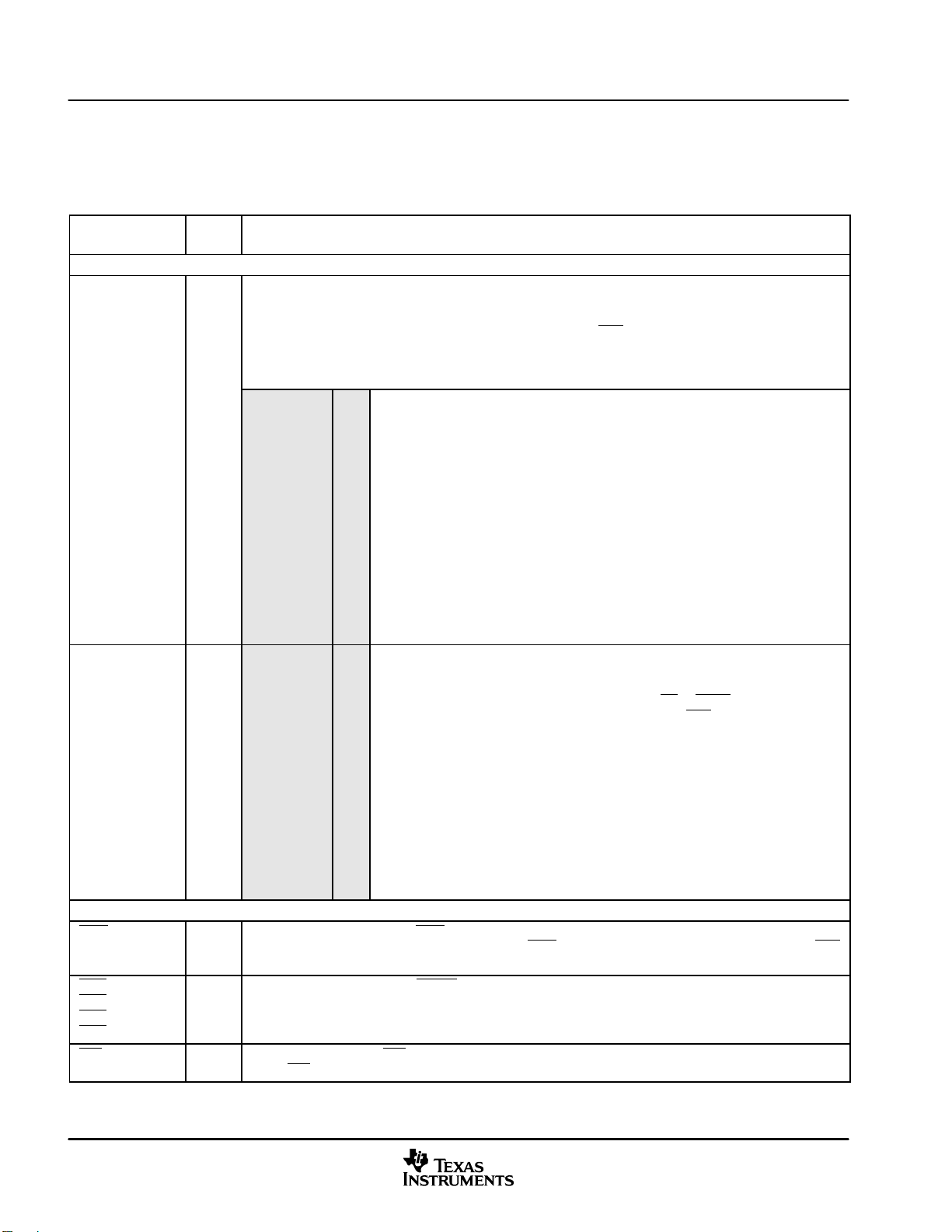
3 Functional Overview
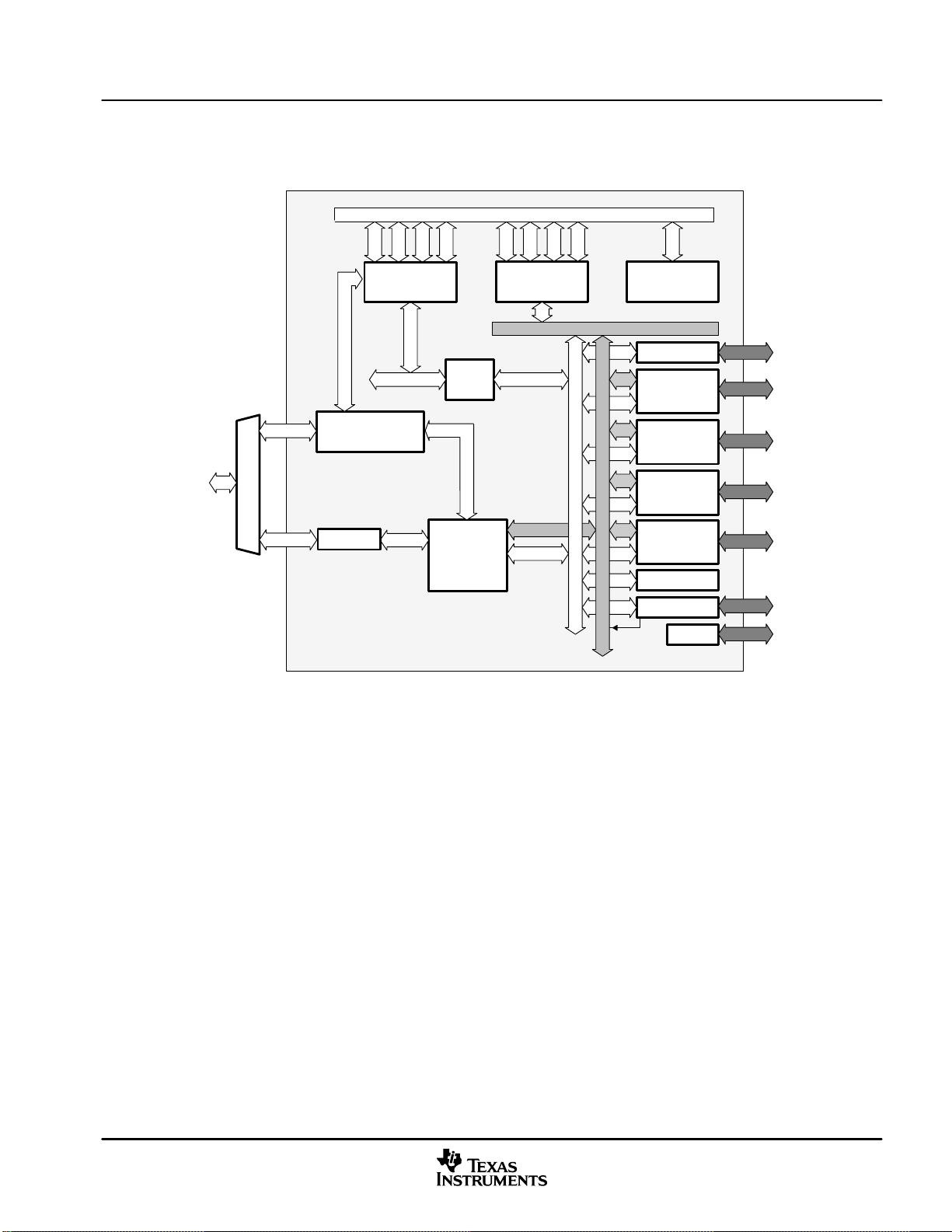
The following functional overview is based on the block diagram in Figure 3−1.
P, C, D, E Buses and Control Signals
Cbus
54X cLEAD
TI BUS
Dbus
Ebus
RHEA
Bridge
Pbus
Cbus
Pbus
40K RAM
Dual Access
Program/Data
RHEA Bus
Dbus
†
Ebus
MBus
Pbus
128K Program
‡
ROM
GPIO
McBSP0
Functional Overview
†
16K for 5404
‡
64K for 5404
Figure 3−1. TMS320VC5407/TMS320VC5404 Functional Block Diagram
3.1 Memory
The 5407/5404 device provides both on-chip ROM and RAM memories to aid in system performance and
integration.
3.1.1 Data Memory
XIO
16HPI
Enhanced XIO
16 HPI
xDMA
logic
RHEAbus
RHEA bus
MBus
MBus
Clocks
McBSP1
McBSP2
UART
TIMER
APLL
JTAG
The data memory space addresses up to 64K of 16-bit words. The device automatically accesses the on-chip
RAM when addressing within its bounds. When an address is generated outside the RAM bounds, the device
automatically generates an external access.
The advantages of operating from on-chip memory are as follows:
• Higher performance because no wait states are required
• Higher performance because of better flow within the pipeline of the central arithmetic logic unit (CALU)
• Lower cost than external memory
• Lower power than external memory
The advantage of operating from off-chip memory is the ability to access a larger address space.
November 2001 − Revised April 2004 SPRS007D
23
Page 24

Functional Overview
3.1.2 Program Memory
Software can configure their memory cells to reside inside or outside of the program address map. When the
cells are mapped into program space, the device automatically accesses them when their addresses are
within bounds. When the program-address generation (PAGEN) logic generates an address outside its
bounds, the device automatically generates an external access. The advantages of operating from on-chip
memory are as follows:
• Higher performance because no wait states are required
• Lower cost than external memory
• Lower power than external memory
The advantage of operating from off-chip memory is the ability to access a larger address space.
3.1.3 Extended Program Memory
The 5407/5404 uses a paged extended memory scheme in program space to allow access of up to 8192K
of program memory. In order to implement this scheme, the 5407/5404 includes several features which are
also present on C548/549/5410:
• Twenty-three address lines, instead of sixteen
• An extra memory-mapped register, the XPC
• Six extra instructions for addressing extended program space
Program memory in the 5407/5404 is organized into 128 pages that are each 64K in length.
The value of the XPC register defines the page selection. This register is memory-mapped into data space
to address 001Eh. At a hardware reset, the XPC is initialized to 0.
3.2 On-Chip ROM With Bootloader
The 5407 features a 128K-word × 16-bit on-chip maskable ROM that is mapped into program memory space,
but 16K words of which can also optionally be mapped into data memory. The 5404 features a 64K-word
16-bit on-chip maskable ROM that is mapped into program memory space.
Customers can also arrange to have the ROM of the 5407/5404 programmed with contents unique to any
particular application.
A bootloader is available in the standard 5407/5404 on-chip ROM. This bootloader can be used to
automatically transfer user code from an external source to anywhere in the program memory at power up.
If MP/MC
on-chip ROM. This location contains a branch instruction to the start of the bootloader program.
The standard 5407/5404 devices provide different ways to download the code to accommodate various
system requirements:
• Parallel from 8-bit or 16-bit-wide EPROM
• Parallel from I/O space, 8-bit or 16-bit mode
• Serial boot from serial ports, 8-bit or 16-bit mode
• UART boot mode
• Host-port interface boot
• Warm boot
of the device is sampled low during a hardware reset, execution begins at location FF80h of the
×
24
November 2001 − Revised April 2004SPRS007D
Page 25
The standard on-chip ROM layout is shown in Table 3−1.
ADDRESS RANGE DESCRIPTION
C000h−D4FFh ROM tables for the GSM EFR speech codec
D500h−F7FFh Reserved
F800h−FBFFh Bootloader
FC00h−FCFFh µ-Law expansion table
FD00h−FDFFh A-Law expansion table
FE00h−FEFFh Sine look-up table
FF00h−FF7Fh Reserved
FF80h−FFFFh Interrupt vector table
†
In the 5407/5404 ROM, 128 words are reserved for factory device-testing purposes. Application
code to be implemented in on-chip ROM must reserve these 128 words at addresses
FF00h−FF7Fh in program space.
3.3 On-Chip RAM
The 5407 device contains 40K-words × 16-bit of on-chip dual-access RAM (DARAM), while the 5404 device
contains 16K-words x 16-bit of DARAM.
The DARAM is composed of five blocks of 8K words each. Each block in the DARAM can support two reads
in one cycle, or a read and a write in one cycle. The five blocks of DARAM on the 5407 are located in the
address range 0080h−9FFFh in data space, and can be mapped into program/data space by setting the OVLY
bit to one.
Table 3−1. Standard On-Chip ROM Layout
†
Functional Overview
†
On the 5404, the two blocks of DARAM are located at 0080h−3FFFh in data space and can also be mapped
into data space by setting OVLY to one.
3.4 On-Chip Memory Security
The 5407/5404 device provides maskable options to protect the contents of on-chip memories. When the
ROM protect option is selected, no externally originating instruction can access the on-chip ROM; when the
RAM protect option is selected, HPI RAM is protected; HPI writes are not restricted, but HPI reads are
restricted to 2000h − 3FFFh.
November 2001 − Revised April 2004 SPRS007D
25
Page 26
Functional Overview
3.5 Memory Maps
3.5.1 5407 Memory Map
Page 0 Program
Hex
0000
007F
0080
9FFF
A000
FF7F
FF80
FFFF
Reserved
(OVLY = 1)
External
(OVLY = 0)
On-Chip
DARAM0−4
(OVLY = 1)
External
(OVLY = 0)
External
Interrupts
(External)
MP/MC
(Microprocessor Mode)
Page 0 Program
= 1
Hex
0000
007F
0080
5FFF
6000
FEFF
FF00
FF7F
FF80
FFFF
Reserved
(OVLY = 1)
External
(OVLY = 0)
On-Chip
DARAM0−2
(OVLY = 1)
External
(OVLY = 0)
On-Chip ROM
(40K x 16-bit)
Reserved
Interrupts
(On-Chip)
= 0
MP/MC
(Microcomputer Mode)
Hex
0000
005F
0060
007F
0080
9FFF
A000
BFFF
C000
FFFF
Memory-Mapped
Figure 3−2. 5407 Program and Data Memory Map
Data
Registers
Scratch-Pad
RAM
On-Chip
DARAM0−4
(40K x 16-bit)
External
On-Chip
PDROM0−1
(DROM=1)
or
External
(DROM=0)
Hex
010000
017FFF
018000
01FFFF
†
The lower 32K words of pages 1 through 127 are only available when the OVLY bit is cleared to 0. If the OVLY bit is set to 1, the on-chip memory
is mapped to the lower 32K words of all program space pages.
Program
External
On-Chip
ROM
Page 1
XPC=1
†
Hex
020000
027FFF
028000
02FFFF
Program
External
On-Chip
ROM
Page 2
XPC=2
†
Hex
030000
038000
03DFFF
03E000
03FFFF
Program
External
On-Chip
ROM
External
Page 3
XPC=3
†
Hex
040000
047FFF037FFF
048000
04FFFF
Program
External
External
Page 4
XPC=4
†
......
Hex
7F0000
7F7FFF
7F8000
7FFFFF
Program
External
External
Page 127
XPC=7Fh
†
Figure 3−3. 5407 Extended Program Memory Map
26
November 2001 − Revised April 2004SPRS007D
Page 27
3.5.2 5404 Memory Map
Page 0 Program
Hex
0000
007F
0080
3FFF
4000
9FFF
A000
FF7F
FF80
FFFF
Reserved
(OVLY = 1)
External
(OVLY = 0)
On-Chip
DARAM0−1
(OVLY = 1)
External
(OVLY = 0)
Reserved
(OVLY = 1)
External
(OVLY = 0)
External
Interrupts
(External)
MP/MC
(Microprocessor Mode)
Page 0 Program
= 1
Hex
0000
007F
0080
3FFF
4000
5FFF
6000
7FFF
8000
FEFF
FF00
FF7F
FF80
FFFF
Reserved
(OVLY = 1)
External
(OVLY = 0)
On-Chip
DARAM0−1
(OVLY = 1)
External
(OVLY = 0)
Reserved
(OVLY = 1)
External
(OVLY = 0)
Reserved
On-Chip ROM
(32K x 16-bit)
Reserved
Interrupts
(On-Chip)
MP/MC
(Microcomputer Mode)
= 0
Hex
0000
005F
0060
007F
0080
3FFF
4000
9FFF
A000
BFFF
C000
FFFF
Memory-Mapped
Figure 3−4. 5404 Program and Data Memory Map
Data
Registers
Scratch-Pad
RAM
On-Chip
DARAM0−1
(32K x 16-bit)
Reserved
External
PDROM0−1
(DROM = 1)
or
External
(DROM = 0)
Functional Overview
November 2001 − Revised April 2004 SPRS007D
27
Page 28
Functional Overview
Hex
010000
013FFF
014000
017FFF
018000
01FFFF
†
The lower 16K words of pages 1 through 127 are only available when the OVLY bit is cleared to 0. If the OVLY bit is set to 1, the on-chip memory
is mapped to the lower 16K words of all program space pages.
Program
External
Reserved
(OVLY = 1)
External
(OVLY = 0)
On-Chip
ROM
Page 1
XPC=1
†
Hex
020000
023FFF
024000
027FFF
028000
02FFFF
Program
External
Reserved
(OVLY = 1)
(OVLY = 0)
Reserved
†
External
Page 2
XPC=2
Hex
030000
034000
037FFF
038000
03DFFF
03E000
03FFFF
Program
External
Reserved
(OVLY = 1)
External
(OVLY = 0)
Reserved
External
Page 3
XPC=3
Hex
040000
†
043FFF033FFF
044000
047FFF
048000
04FFFF
Program
External
Reserved
(OVLY = 1)
External
(OVLY = 0)
External
Page 4
XPC=4
†
......
Hex
7F0000
7F3FFF
7F4000
7F7FFF
7F8000
7FFFFF
Program
External
Reserved
(OVLY = 1)
External
(OVLY = 0)
External
Page 127
XPC=7Fh
†
Figure 3−5. 5404 Extended Program Memory Map
3.5.3 Relocatable Interrupt Vector Table
The reset, interrupt, and trap vectors are addressed in program space. These vectors are soft — meaning that
the processor, when taking the trap, loads the program counter (PC) with the trap address and executes the
code at the vector location. Four words, either two 1-word instructions or one 2-word instruction, are reserved
at each vector location to accommodate a delayed branch instruction which allows branching to the
appropriate interrupt service routine without the overhead.
At device reset, the reset, interrupt, and trap vectors are mapped to address FF80h in program space.
However, these vectors can be remapped to the beginning of any 128-word page in program space after
device reset. This is done by loading the interrupt vector pointer (IPTR) bits in the PMST register with the
appropriate 128-word page boundary address. After loading IPTR, any user interrupt or trap vector is mapped
to the new 128-word page.
NOTE: The hardware reset (RS
with 1s. Therefore, the reset vector is always fetched at location FF80h in program space.
) vector cannot be remapped because the hardware reset loads the IPTR
28
November 2001 − Revised April 2004SPRS007D
Page 29
15
RESET
Functional Overview
IPTR
R/W-1FF
7
IPTR MP/MC OVLY AVIS DROM CLKOFF SMUL SST
LEGEND: R = Read, W = Write, n = value after reset
654321 0
MP/MC Pin R/W-0 R/W-0 R/W-0 R/W-0 R/W-0 R/W-0
Figure 3−6. Processor Mode Status (PMST) Register
Table 3−2. Processor Mode Status (PMST) Register Bit Fields
BIT
NO. NAME
15−7 IPTR 1FFh
6 MP/MC
5 OVLY 0
4 AVIS 0
3 DROM 0
2 CLKOFF 0
1 SMUL N/A
0 SST N/A
RESET
VALUE
MP/MC
pin
FUNCTION
Interrupt vector pointer. The 9-bit IPTR field points to the 128-word program page where the interrupt
vectors reside. The interrupt vectors can be remapped to RAM for boot-loaded operations. At reset, these
bits are all set to 1; the reset vector always resides at address FF80h in program memory space. The
RESET instruction does not affect this field.
Microprocessor/microcomputer mode. MP/MC enables/disables the on-chip ROM to be addressable in
program memory space.
- MP/MC
- MP/MC
MP/MC
pin is not sampled again until the next reset. The RESET instruction does not affect this bit. This bit can
also be set or cleared by software.
RAM overlay. OVLY enables on-chip dual-access data RAM blocks to be mapped into program space.
The values for the OVLY bit are:
- OVLY = 0: The on-chip RAM is addressable in data space but not in program space.
- OVLY = 1: The on-chip RAM is mapped into program space and data space. Data page 0 (addresses
Address visibility mode. AVIS enables/disables the internal program address to be visible at the
address pins.
- AVIS = 0: The external address lines do not change with the internal program address. Control and
- AVIS = 1: This mode allows the internal program address to appear at the pins of the 5407/5404 so
Data ROM. DROM enables on-chip ROM to be mapped into data space. The DROM bit values are:
- DROM = 0: The on-chip ROM is not mapped into data space.
- DROM = 1: A portion of the on-chip ROM is not mapped into data space.
The SWSM bit of the SWCR defines a multiplication factor of 1 or 2 for the base number of wait states.
CLOCKOUT off. When the CLKOFF bit is 1, the output of CLKOUT is disabled and remains at a high
level.
Saturation on multiplication. When SMUL = 1, saturation of a multiplication result occurs before
performing the accumulation in a MAC of MAS instruction. The SMUL bit applies only when OVM = 1
and FRCT = 1.
Saturation on store. When SST = 1, saturation of the data from the accumulator is enabled before
storing in memory. The saturation is performed after the shift operation.
= 0: The on-chip ROM is enabled and addressable.
= 1: The on-chip ROM is not available.
is set to the value corresponding to the logic level on the MP/MC pin when sampled at reset. This
0h to 7Fh), however, is not mapped into program space.
data lines are not affected and the address bus is driven with the last address on the bus.
that the internal program address can be traced. Also, it allows the interrupt vector to be decoded
in conjunction with IACK
when the interrupt vectors reside on on-chip memory.
November 2001 − Revised April 2004 SPRS007D
29
Page 30

Functional Overview
3.6 On-Chip Peripherals
The 5407/5404 device has the following peripherals:
• Software-programmable wait-state generator
• Programmable bank-switching
• A host-port interface (HPI8/16)
• Three multichannel buffered serial ports (McBSPs)
• Two hardware timers
• A clock generator with a multiple phase-locked loop (PLL)
• Enhanced external parallel interface (XIO2)
• A DMA controller (DMA)
• A UART with an integrated baud rate generator
3.6.1 Software-Programmable Wait-State Generator
The software wait-state generator of the 5407/5404 can extend external bus cycles by up to fourteen machine
cycles. Devices that require more than fourteen wait states can be interfaced using the hardware READY line.
When all external accesses are configured for zero wait states, the internal clocks to the wait-state generator
are automatically disabled. Disabling the wait-state generator clocks reduces the power consumption of
the 5407/5404.
The software wait-state register (SWWSR) controls the operation of the wait-state generator. The 14 LSBs
of the SWWSR specify the number of wait states (0 to 7) to be inserted for external memory accesses to five
separate address ranges. This allows a different number of wait states for each of the five address ranges.
Additionally, the software wait-state multiplier (SWSM) bit of the software wait-state control register (SWCR)
defines a multiplication factor of 1 or 2 for the number of wait states. At reset, the wait-state generator is
initialized to provide seven wait states on all external memory accesses. The SWWSR bit fields are shown
in Figure 3−7 and described in Table 3−3.
15
XPA I/O DATA DATA
R/W-0 R/W-111 R/W-111
DATA PROGRAM PROGRAM
R/W-111 R/W-111 R/W-111
LEGEND: R = Read, W = Write, n = value after reset
14 12 11 9 8
65 32 0
Figure 3−7. Software Wait-State Register (SWWSR) [Memory-Mapped Register (MMR) Address 0028h]
30
November 2001 − Revised April 2004SPRS007D
Page 31
Table 3−3. Software Wait-State Register (SWWSR) Bit Fields
RESET
RESET
BIT
NO. NAME
15 XPA 0
14−12 I/O 111
11−9 Data 111
8−6 Data 111
5−3 Program 111
2−0 Program 111
RESET
VALUE
Functional Overview
FUNCTION
Extended program address control bit. XPA is used in conjunction with the program space fields
(bits 0 through 5) to select the address range for program space wait states.
I/O space. The field value (0−7) corresponds to the base number of wait states for I/O space accesses
within addresses 0000−FFFFh. The SWSM bit of the SWCR defines a multiplication factor of 1 or 2 for
the base number of wait states.
Upper data space. The field value (0−7) corresponds to the base number of wait states for external
data space accesses within addresses 8000−FFFFh. The SWSM bit of the SWCR defines a
multiplication factor of 1 or 2 for the base number of wait states.
Lower data space. The field value (0−7) corresponds to the base number of wait states for external
data space accesses within addresses 0000−7FFFh. The SWSM bit of the SWCR defines a
multiplication factor of 1 or 2 for the base number of wait states.
Upper program space. The field value (0−7) corresponds to the base number of wait states for external
program space accesses within the following addresses:
- XPA = 0: xx8000 − xxFFFFh
- XPA = 1: 400000h − 7FFFFFh
The SWSM bit of the SWCR defines a multiplication factor of 1 or 2 for the base number of wait states.
Lower program space. The field value (0−7) corresponds to the base number of wait states for external
program space accesses within the following addresses:
- XPA = 0: xx0000 − xx7FFFh
- XPA = 1: 000000 − 3FFFFFh
The SWSM bit of the SWCR defines a multiplication factor of 1 or 2 for the base number of wait states.
The software wait-state multiplier bit of the software wait-state control register (SWCR) is used to extend the
base number of wait states selected by the SWWSR. The SWCR bit fields are shown in Figure 3−8 and
described in Table 3−4.
15
LEGEND: R = Read, W = Write, n = value after reset
Figure 3−8. Software Wait-State Control Register (SWCR) [MMR Address 002Bh]
Table 3−4. Software Wait-State Control Register (SWCR) Bit Fields
PIN
NO. NAME
15−1 Reserved 0
0 SWSM 0
RESET
VALUE
These bits are reserved and are unaffected by writes.
Software wait-state multiplier. Used to multiply the number of wait states defined in the SWWSR by a factor
of 1 or 2.
- SWSM = 0: wait-state base values are unchanged (multiplied by 1).
- SWSM = 1: wait-state base values are multiplied by 2 for a maximum of 14 wait states.
Reserved
R/W-0
10
Reserved SWSM
R/W-0 R/W-0
FUNCTION
November 2001 − Revised April 2004 SPRS007D
31
Page 32

Functional Overview
15
CONSEC
1
CONSEC 1:
Consecutive bank switches on external memory reads. Each read cycle consists of 3 cycles:
12
IACKOFF
1
2
HBH
0
1BH0
3.6.2 Programmable Bank-Switching
Programmable bank-switching logic allows the 5407/5404 to switch between external memory banks without
requiring external wait states for memories that need additional time to turn off. The bank-switching logic
automatically inserts one cycle when accesses cross a 32K-word memory-bank boundary inside program or
data space.
Bank-switching is defined by the bank-switching control register (BSCR), which is memory-mapped at
address 0029h. The bit fields of the BSCR are shown in Figure 3−9 and are described in Table 3−5.
15
CONSEC DIVFCT IACKOFF Reserved
R/W-1 R/W-11 R/W-1 R
LEGEND: R = Read, W = Write, n = value after reset
14 13 12 11
321 0
Reserved HBH BH Reserved
R R/W-0 R
Figure 3−9. Bank-Switching Control Register (BSCR) [MMR Address 0029h]
Table 3−5. Bank-Switching Control Register (BSCR) Fields
†
RESET
VALUE
1
FUNCTION
Consecutive bank-switching. Specifies the bank-switching mode.
CONSEC = 0:
CONSEC = 1:
CLKOUT output divide factor. The CLKOUT output is driven by an on-chip source having a frequency
equal to 1/(DIVFCT+1) of the DSP clock.
DIVFCT = 00: CLKOUT is not divided.
DIVFCT = 01: CLKOUT is divided by 2 from the DSP clock.
DIVFCT = 10: CLKOUT is divided by 3 from the DSP clock.
DIVFCT = 11: CLKOUT is divided by 4 from the DSP clock (default value following reset).
IACK signal output off. Controls the output of the IACK signal. IACKOFF is set to 1 at reset.
IACKOFF = 0: The IACK signal output off function is disabled.
IACKOFF = 1: The IACK signal output off function is enabled.
HPI bus holder. Controls the HPI bus holder. HBH is cleared to 0 at reset.
HBH = 0: The bus holder is disabled except when HPI16=1.
HBH = 1:
Bus holder. Controls the bus holder. BH is cleared to 0 at reset.
BH = 0: The bus holder is disabled.
BH = 1:
Bank-switching on 32K bank boundaries only. This bit is cleared if fast access is desired for
continuous memory reads (i.e., no starting and trailing cycles between read cycles).
Consecutive bank switches on external memory reads. Each read cycle consists of 3 cycles:
starting cycle, read cycle, and trailing cycle.
The bus holder is enabled. When not driven, the HPI data bus, HD[7:0] is held in the previous
logic level.
The bus holder is enabled. When not driven, the data bus, D[15:0] is held in the previous logic
level.
BIT NAME
15 CONSEC
13−14 DIVFCT 11
12 IACKOFF 1
11−3 Reserved − Reserved
0 Reserved − Reserved
†
For additional information, see Section 3.11 of this document.
32
November 2001 − Revised April 2004SPRS007D
Page 33

Functional Overview
The 5407/5404 has an internal register that holds the MSB of the last address used for a read or write operation
in program or data space. In the non-consecutive bank switches (CONSEC
used for the current read does not match that contained in this internal register, the MSTRB
= 0), if the MSB of the address
(memory strobe)
signal is not asserted for one CLKOUT cycle. During this extra cycle, the address bus switches to the new
address. The contents of the internal register are replaced with the MSB for the read of the current address.
If the MSB of the address used for the current read matches the bits in the register, a normal read cycle occurs.
In non-consecutive bank switches (CONSEC
= 0), if repeated reads are performed from the same memory
bank, no extra cycles are inserted. When a read is performed from a different memory bank, memory conflicts
are avoided by inserting an extra cycle. For more information, see Section 3.11 of this document.
The bank-switching mechanism automatically inserts one extra cycle in the following cases:
• A memory read followed by another memory read from a different memory bank.
• A program-memory read followed by a data-memory read.
• A data-memory read followed by a program-memory read.
• A program-memory read followed by another program-memory read from a different page.
3.6.3 Bus Holders
The 5407/5404 has two bus holder control bits, BH (BSCR[1]) and HBH (BSCR[2]), to control the bus keepers
of the address bus (A[17−0]), data bus (D[15−0]), and the HPI data bus (HD[7−0]). Bus keeper
enabling/disabling is described in Table 3−5.
Table 3−6. Bus Holder Control Bits
HPI16 PIN BH HBH D[15−0] A[17−0] HD[7−0]
0 0 0 OFF OFF OFF
0 0 1 OFF OFF ON
0 1 0 ON OFF OFF
0 1 1 ON OFF ON
1 0 0 OFF OFF ON
1 0 1 OFF ON ON
1 1 0 ON OFF ON
1 1 1 ON ON ON
3.7 Parallel I/O Ports
The 5407/5404 has a total of 64K I/O ports. These ports can be addressed by the PORTR instruction or the
PORTW instruction. The IS
signal indicates a read/write operation through an I/O port. The 5407/5404 can
interface easily with external devices through the I/O ports while requiring minimal off-chip address-decoding
circuits.
3.7.1 Enhanced 8-/16-Bit Host-Port Interface (HPI8/16)
The 5407/5404 host-port interface, also referred to as the HPI8/16, is an enhanced version of the standard
8-bit HPI found on earlier TMS320C54x DSPs (542, 545, 548, and 549). The 5407/5404 HPI can be used
to interface to an 8-bit or 16-bit host. When the address and data buses for external I/O is not used (to interface
to external devices in program/data/IO spaces), the 5407/5404 HPI can be configured as an HPI16 to interface
to a 16-bit host. This configuration can be accomplished by connecting the HPI16 pin to logic “1”.
November 2001 − Revised April 2004 SPRS007D
33
Page 34

Functional Overview
When the HPI16 pin is connected to a logic “0”, the 5407/5404 HPI is configured as an HPI8. The HPI8 is an
8-bit parallel port for interprocessor communication. The features of the HPI8 include:
Standard features:
• Sequential transfers (with autoincrement) or random-access transfers
• Host interrupt and C54x interrupt capability
• Multiple data strobes and control pins for interface flexibility
The HPI8 interface consists of an 8-bit bidirectional data bus and various control signals. Sixteen-bit transfers
are accomplished in two parts with the HBIL input designating high or low byte. The host communicates with
the HPI8 through three dedicated registers — the HPI address register (HPIA), the HPI data register (HPID),
and the HPI control register (HPIC). The HPIA and HPID registers are only accessible by the host, and the
HPIC register is accessible by both the host and the 5407/5404.
Enhanced features:
• Access to entire on-chip RAM through DMA bus
• Capability to continue transferring during emulation stop
The HPI16 is an enhanced 16-bit version of the TMS320C54x DSP 8-bit host-port interface (HPI8). The
HPI16 is designed to allow a 16-bit host to access the DSP on-chip memory, with the host acting as the master
of the interface. Some of the features of the HPI16 include:
• 16-bit bidirectional data bus
• Multiple data strobes and control signals to allow glueless interfacing to a variety of hosts
• Only nonmultiplexed address/data modes are supported
• 18-bit address bus used in nonmultiplexed mode to allow access to all internal memory (including internal
extended address pages)
• HRDY signal to hold off host accesses due to DMA latency
• The HPI16 acts as a slave to a 16-bit host processor and allows access to the on-chip memory of the DSP.
NOTE: Only the nonmultiplexed mode is supported when the 5407/5404 HPI is configured as
a HPI16 (see Figure 3−10).
The 5407/5404 HPI functions as a slave and enables the host processor to access the on-chip memory. A
major enhancement to the 5407/5404 HPI over previous versions is that it allows host access to the entire
on-chip memory range of the DSP. The host and the DSP both have access to the on-chip RAM at all times
and host accesses are always synchronized to the DSP clock. If the host and the DSP contend for access to
the same location, the host has priority, and the DSP waits for one cycle. Note that since host accesses are
always synchronized to the 5407/5404 clock, an active input clock (CLKIN) is required for HPI accesses during
IDLE states, and host accesses are not allowed while the 5407/5404 reset pin is asserted.
34
November 2001 − Revised April 2004SPRS007D
Page 35
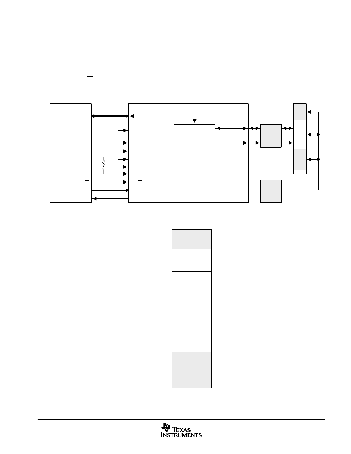
3.7.2 HPI Nonmultiplexed Mode
In nonmultiplexed mode, a host with separate address/data buses can access the HPI16 data register (HPID)
via the HD 16-bit bidirectional data bus, and the address register (HPIA) via the 23-bit HA address bus. The
host initiates the access with the strobe signals (HDS1
with the HR/W
is not available in nonmultiplexed mode since there are no HCNTL signals available. All host accesses initiate
a DMA read or write access. Figure 3−10 shows a block diagram of the HPI16 in nonmultiplexed mode.
signal. The HPI16 can stall host accesses via the HRDY signal. Note that the HPIC register
Functional Overview
, HDS2, HCS) and controls the direction of the access
HOST
DATA[15:0]
Address[22:0]
R/W
Data Strobes
READY
PPD[15:0]
V
CC
HRDY
HINT
HCNTL0
HCNTL1
HBIL
HAS
HR/W
HDS1, HDS2, HCS
HPI16
HPID[15:0]
Figure 3−10. Host-Port Interface — Nonmultiplexed Mode
Address (Hex)
0000
Reserved
005F
0060
DARAM0
1FFF
2000
DARAM1
3FFF
4000
DARAM2
5FFF
6000
DARAM3
7FFF
8000
DARAM4
9FFF
A000
†
†
†
DMA
54xx
CPU
Internal
Memory
Reserved
FFFF
†
Reserved on 5404 devices
Figure 3−11. HPI Memory Map
November 2001 − Revised April 2004 SPRS007D
35
Page 36

Functional Overview
3.8 Multichannel Buffered Serial Ports (McBSPs)
The 5407/5404 device provides three high-speed, full-duplex, multichannel buffered serial ports that allow
direct interface to other C54x/LC54x devices, codecs, and other devices in a system. The McBSPs are based
on the standard serial-port interface found on other 54x devices. Like their predecessors, the McBSPs provide:
• Full-duplex communication
• Double-buffer data registers, which allow a continuous data stream
• Independent framing and clocking for receive and transmit
In addition, the McBSPs have the following capabilities:
• Direct interface to:
− T1/E1 framers
− MVIP switching compatible and ST-BUS compliant devices
− IOM-2 compliant devices
− AC97-compliant devices
− IIS-compliant devices
− Serial peripheral interface
• Multichannel transmit and receive of up to 128 channels
• A wide selection of data sizes, including 8, 12, 16, 20, 24, or 32 bits
•µ-law and A-law companding
• Programmable polarity for both frame synchronization and data clocks
• Programmable internal clock and frame generation
The McBSP consists of a data path and control path. The six pins, BDX, BDR, BFSX, BFSR, BCLKX, and
BCLKR, connect the control and data paths to external devices. The implemented pins can be programmed
as general-purpose I/O pins if they are not used for serial communication. Note that on McBSP2, the transmit
and receive clocks and the transmit and receive frame sync have been combined.
The data is communicated to devices interfacing to the McBSP by way of the data transmit (BDX) pin for
transmit and the data receive (BDR) pin for receive. The CPU or DMA reads the received data from the data
receive register (DRR) and writes the data to be transmitted to the data transmit register (DXR). Data written
to the DXR is shifted out to BDX by way of the transmit shift register (XSR). Similarly, receive data on the BDR
pin is shifted into the receive shift register (RSR) and copied into the receive buffer register (RBR). RBR is then
copied to DRR, which can be read by the CPU or DMA. This allows internal data movement and external data
communications simultaneously.
Control information in the form of clocking and frame synchronization is communicated by way of BCLKX,
BCLKR, BFSX, and BFSR. The device communicates to the McBSP by way of 16-bit-wide control registers
accessible via the internal peripheral bus.
The control block consists of internal clock generation, frame synchronization signal generation, and their
control, and multichannel selection. This control block sends notification of important events to the CPU and
DMA by way of two interrupt signals, XINT and RINT, and two event signals, XEVT and REVT.
The on-chip companding hardware allows compression and expansion of data in either µ-law or A-law format.
When companding is used, transmitted data is encoded according to the specified companding law and
received data is decoded to 2s complement format.
The sample rate generator provides the McBSP with several means of selecting clocking and framing for both
the receiver and transmitter. Both the receiver and transmitter can select clocking and framing independently.
36
November 2001 − Revised April 2004SPRS007D
Page 37

Functional Overview
The McBSP allows the multiple channels to be independently selected for the transmitter and receiver. When
multiple channels are selected, each frame represents a time-division multiplexed (TDM) data stream. In using
time-division multiplexed data streams, the CPU may only need to process a few of them. Thus, to save
memory and bus bandwidth, multichannel selection allows independent enabling of particular channels for
transmission and reception. All 128 channels in a bit stream consisting of a maximum of 128 channels can
be enabled.
15
Reserved XMCME XPBBLK
R R/W R/W
7
XPBBLK
R/W R/W R R/W
LEGEND: R = Read, W = Write
654 21 0
XPABLK XCBLK XMCM
10 9 8
Figure 3−12. Multichannel Control Register (MCR1)
15
Reserved RMCME RPBBLK
R R/W R/W
7
RPBBLK
R/W R/W R R R/W
654 21 0
RPABLK RCBLK Reserved RMCM
10 9 8
LEGEND: R = Read, W = Write
Figure 3−13. Multichannel Control Register (MCR2)
The 5407/5404 McBSP has two working modes:
• In the first mode, when (R/X)MCME = 0, it is comparable with the McBSPs used in the 5410 where the
normal 32-channel selection is enabled (default).
• In the second mode, when (R/X)MCME = 1, it has 128-channel selection capability. Multichannel control
register Bit 9, (R/X)MCME, is used as the 128-channel selection enable bit. Once (R/X)MCME = 1, twelve
new registers ((R/X)CERC − (R/X)CERH) are used to enable the 128-channel selection.
The clock stop mode (CLKSTP) in the McBSP provides compatibility with the serial port interface protocol.
Clock stop mode works with only single-phase frames and one word per frame. The word sizes supported by
the McBSP are programmable for 8-, 12-, 16-, 20-, 24-, or 32-bit operation. When the McBSP is configured
to operate in SPI mode, both the transmitter and the receiver operate together as a master or as a slave.
Although the BCLKS pin is not available on the 5407/5404 PGE and GGU packages, the 5407/5404 is capable
of synchronization to external clock sources. BCLKX or BCLKR can be used by the sample rate generator for
external synchronization. The sample rate clock mode extended (SCLKME) bit field is located in the PCR to
accommodate this option.
November 2001 − Revised April 2004 SPRS007D
37
Page 38

Functional Overview
15
Reserved XIOEN RIOEN FSXM FSRM CLKXM CLKRM
R/W R/W R/W R/W R/W R/W R/W
7
SCLKME
R/W R/W R/W R/W R/W R/W R/W R/W
LEGEND: R = Read, W = Write
14 13 12 11 10 9 8
654321 0
CLKS STAT DX STAT DR STAT FSXP FSRP CLKXP CLKRP
Figure 3−14. Pin Control Register (PCR)
The selection of sample rate input clock is made by the combination of the CLKSM (bit 13 in SRGR2) bit value
and the SCLKME bit value as shown in Table 3−7.
Table 3−7. Sample Rate Input Clock Selection
SCLKME CLKSM SAMPLE RATE CLOCK MODE
0 0 Reserved (CLKS pin unavailable)
0 1 CPU clock
1 0 BCLKR
1 1 BCLKX
When the SCLKME bit is cleared to 0, the CLKSM bit is used, as before, to select either the CPU clock or the
CLKS pin (not bonded out on the 5407/5404 device package) as the sample rate input clock. Setting the
SCLKME bit to 1 enables the CLKSM bit to select between the BCLKR pin or BCLKX pin for the sample rate
input clock.
When either the BCLKR or CLKX is configured this way, the output buffer for the selected pin is automatically
disabled. For example, with SCLKME = 1 and CLKSM = 0, the BCLKR pin is configured as the input of the
sample rate generator. Both the transmitter and receiver circuits can be synchronized to the sample rate
generator output by setting the CLKXM and CLKRM bits of the pin configuration register (PCR) to 1. Note that
the sample rate generator output will only be driven on the BCLKX pin since the BCLKR output buffer is
automatically disabled.
The McBSP is fully static and operates at arbitrary low clock frequencies. For maximum operating frequency,
see Section 5.14.
3.9 Hardware Timers
The 5407/5404 device features two 16-bit timing circuits with 4-bit prescalers. The timer counters are
decremented by one every CPU clock cycle. Each time the counter decrements to 0, a timer interrupt is
generated. The timer can be stopped, restarted, reset, or disabled by specific status bits.
Both timers can be use to generate interrupts to the CPU, however, the second timer (Timer1) has its interrupt
combined with external interrupt 3 (INT3
the INT3
in reset).
Since the Timer1 output is multiplexed externally with the HINT
input pin = 0) if the Timer1 output is to be used. The Timer1 output also has a dedicated enable bit in the
General Purpose I/O Control Register (GPIOCR) located at data memory address 003Ch. If the external
Timer1 output is to be used, in addition to disabling the HPI, the TOUT1 bit in the GPIOCR must also be set
to 1.
input should be disabled (tied high), and to use the INT3 input, the timer should be disabled (placed
) in the interrupt flag register. Therefore, to use the Timer1 interrupt,
output, the HPI must be disabled (HPIENA
38
November 2001 − Revised April 2004SPRS007D
Page 39
3.10 Clock Generator
The clock generator provides clocks to the 5407/5404 device, and consists of a phase-locked loop (PLL)
circuit. The clock generator requires a reference clock input, which can be provided from an external clock
source. The reference clock input is then divided by two (DIV mode) to generate clocks for the 5407/5404
device, or the PLL circuit can be used (PLL mode) to generate the device clock by multiplying the reference
clock frequency by a scale factor, allowing use of a clock source with a lower frequency than that of the CPU.
The PLL is an adaptive circuit that, once synchronized, locks onto and tracks an input clock signal.
When the PLL is initially started, it enters a transitional mode during which the PLL acquires lock with the input
signal. Once the PLL is locked, it continues to track and maintain synchronization with the input signal. Then,
other internal clock circuitry allows the synthesis of new clock frequencies for use as master clock for the
5407/5404 device.
This clock generator allows system designers to select the clock source. The sources that drive the clock
generator are:
• A crystal resonator circuit. The crystal resonator circuit is connected across the X1 and X2/CLKIN pins
of the 5407/5404 to enable the internal oscillator.
• An external clock. The external clock source is directly connected to the X2/CLKIN pin, and X1 is left
unconnected.
The software-programmable PLL features a high level of flexibility, and includes a clock scaler that provides
various clock multiplier ratios, capability to directly enable and disable the PLL, and a PLL lock timer that can
be used to delay switching to PLL clocking mode of the device until lock is achieved. Devices that have a
built-in software-programmable PLL can be configured in one of two clock modes:
Functional Overview
• PLL mode. The input clock (X2/CLKIN) is multiplied by 1 of 31 possible ratios.
• DIV (divider) mode. The input clock is divided by 2 or 4. Note that when DIV mode is used, the PLL can
be completely disabled in order to minimize power dissipation.
The software-programmable PLL is controlled using the 16-bit memory-mapped (address 0058h) clock mode
register (CLKMD). The CLKMD register is used to define the clock configuration of the PLL clock module. Note
that upon reset, the CLKMD register is initialized with a predetermined value dependent only upon the state
of the CLKMD1 − CLKMD3 pins. For more programming information, see the TMS320C54x DSP Reference
Set, Volume 1: CPU and Peripherals (literature number SPRU131). The CLKMD pin configured clock options
are shown in Table 3−8.
Table 3−8. Clock Mode Settings at Reset
CLKMD1 CLKMD2 CLKMD3
0 0 0 0000h 1/2 (PLL and oscillator disabled)
0 0 1 9007h PLL x 10
0 1 0 4007h PLL x 5
1 0 0 1007h PLL x 2
1 1 0 F007h PLL x 1
1 0 1 F000h 1/4 (PLL disabled)
1 1 1 0000h 1/2 (PLL disabled)
0 1 1 — Reserved
†
The external CLKMD1−CLKMD3 pins are sampled to determine the desired clock generation mode
while RS
clock mode register in software.
is low. Following reset, the clock generation mode can be reconfigured by writing to the internal
CLKMD RESET
VALUE
CLOCK MODE
†
November 2001 − Revised April 2004 SPRS007D
39
Page 40

Functional Overview
3.11 Enhanced External Parallel Interface (XIO2)
The 5407/5404 external interface has been redesigned to include several improvements, including:
simplification of the bus sequence, more immunity to bus contention when transitioning between read and
write operations, the ability for external memory access to the DMA controller, and optimization of the
power-down modes.
The bus sequence on the 5407/5404 still maintains all of the same interface signals as on previous 54x
devices, but the signal sequence has been simplified. Most external accesses now require 3 cycles composed
of a leading cycle, an active (read or write) cycle, and a trailing cycle. The leading and trailing cycles provide
additional immunity against bus contention when switching between read operations and write operations. To
maintain high-speed read access, a consecutive read mode that performs single-cycle reads as on previous
54x devices is available.
Figure 3−15 shows the bus sequence for three cases: all I/O reads, memory reads in nonconsecutive mode,
or single memory reads in consecutive mode. The accesses shown in Figure 3−15 always require 3 CLKOUT
cycles to complete.
CLKOUT
A[22:0]
D[15:0]
R/W
MSTRB or IOSTRB
PS/DS/IS
Leading
Cycle
READ
Read
Cycle
Trailing
Cycle
Figure 3−15. Nonconsecutive Memory Read and I/O Read Bus Sequence
40
November 2001 − Revised April 2004SPRS007D
Page 41
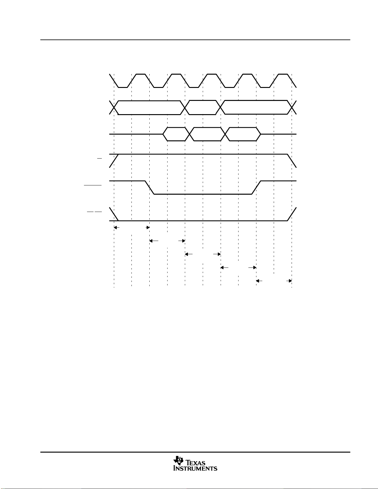
Functional Overview
Figure 3−16 shows the bus sequence for repeated memory reads in consecutive mode. The accesses shown
in Figure 3−16 require (2+n) CLKOUT cycles to complete, where n is the number of consecutive reads
performed.
CLKOUT
A[22:0]
D[15:0]
R/W
MSTRB
PS/DS
Leading
Cycle
READ
Read
Cycle
READ
Read
Cycle
READ
Read
Cycle
Trailing
Cycle
Figure 3−16. Consecutive Memory Read Bus Sequence (n = 3 reads)
November 2001 − Revised April 2004 SPRS007D
41
Page 42

Functional Overview
Figure 3−17 shows the bus sequence for all memory writes and I/O writes. The accesses shown in
Figure 3−17 always require 3 CLKOUT cycles to complete.
CLKOUT
A[22:0]
WRITE
Write
Cycle
Trailing
Cycle
MSTRB
D[15:0]
R/W
or IOSTRB
PS/DS/IS
Leading
Cycle
Figure 3−17. Memory Write and I/O Write Bus Sequence
The enhanced interface also provides the ability for DMA transfers to extend to external memory. For more
information on DMA capability, see the DMA sections that follow.
The enhanced interface improves the low-power performance already present on the TMS320C5000 DSP
platform by switching off the internal clocks to the interface when it is not being used. This power-saving feature
is automatic, requires no software setup, and causes no latency in the operation of the interface.
Additional features integrated in the enhanced interface are the ability to automatically insert bank-switching
cycles when crossing 32K memory boundaries (see Section 3.6.2), the ability to program up to 14 wait states
through software (see Section 3.6.1), and the ability to divide down CLKOUT by a factor of 1, 2, 3, or 4. Dividing
down CLKOUT provides an alternative to wait states when interfacing to slower external memory or peripheral
devices. While inserting wait states extends the bus sequence during read or write accesses, it does not slow
down the bus signal sequences at the beginning and the end of the access. Dividing down CLKOUT provides
a method of slowing the entire bus sequence when necessary. The CLKOUT divide-down factor is controlled
through the DIVFCT field in the bank-switching control register (BSCR) (see Table 3−5).
3.12 DMA Controller
The 5407/5404 direct memory access (DMA) controller transfers data between points in the memory map
without intervention by the CPU. The DMA allows movements of data to and from internal program/data
memory, internal peripherals (such as the McBSPs, but not the UART), or external memory devices to occur
in the background of CPU operation. The DMA has six independent programmable channels, allowing six
different contexts for DMA operation.
TMS320C5000 is a trademark of Texas Instruments.
42
November 2001 − Revised April 2004SPRS007D
Page 43
3.12.1 Features
The DMA has the following features:
• The DMA operates independently of the CPU.
• The DMA has six channels. The DMA can keep track of the contexts of six independent block transfers.
• The DMA has higher priority than the CPU for both internal and external accesses.
• Each channel has independently programmable priorities.
• Each channel’s source and destination address registers can have configurable indexes through memory
on each read and write transfer, respectively. The address may remain constant, be post-incremented,
be post-decremented, or be adjusted by a programmable value.
• Each read or write internal transfer may be initialized by selected events.
• On completion of a half- or entire-block transfer, each DMA channel may send an interrupt to the CPU.
• The DMA can perform double-word internal transfers (a 32-bit transfer of two 16-bit words).
3.12.2 DMA External Access
The 5407/5404 DMA supports external accesses to extended program, extended data, and extended I/O
memory. These overlay pages are only visible to the DMA controller. A maximum of two DMA channels can
be used for external memory accesses. The DMA external accesses require a minimum of 8 cycles for external
writes and a minimum of 11 cycles for external reads assuming the XIO02 is in consecutive mode
(CONSEC
The control of the bus is arbitrated between the CPU and the DMA. While the DMA or CPU is in control of the
external bus, the other will be held-off via wait states until the current transfer is complete. The DMA takes
precedence over XIO requests.
= 1), wait state is set to two, and CLKOUT is not divided (DIVFCT = 00).
Functional Overview
• Only two channels are available for external accesses. (One for external reads and one for external
writes.)
• Single-word (16-bit) transfers are supported for external accesses.
• The DMA does not support transfers from the peripherals to external memory.
• The DMA does not support transfers from external memory to the peripherals.
• The DMA does not support external-to-external transfers.
• The DMA does not support synchronized external transfers.
15
AUTOINIT DINM IMOD CTMOD SLAXS SIND
7
DMS
14 13 12 11 10 8
654 21 0
DLAXS DIND DMD
Figure 3−18. DMA Transfer Mode Control Register (DMMCRn)
These new bit fields were created to allow the user to define the space-select for the DMA (internal/external).
Also, a new extended destination data page (XDSTDP[6:0], subaddress 029h) and extended source data
page (XSRCDP[6:0], subaddress 028h) have been created. The functions of the DLAXS and SLAXS bits are
as follows:
DLAXS(DMMCRn[5]) Destination
0 = No external access (default internal)
1 = External access
SLAXS(DMMCRn[11]) Source 0 = No external access (default internal)
1 = External access
November 2001 − Revised April 2004 SPRS007D
43
Page 44

Functional Overview
Table 3−9 lists the DMD bit values and their corresponding destination space.
Table 3−9. DMD Section of the DMMCRn Register
For the CPU external access, software can configure the memory cells to reside inside or outside the program
address map. When the cells are mapped into program space, the device automatically accesses them when
their addresses are within bounds. When the address generation logic generates an address outside its
bounds, the device automatically generates an external access.
Two new registers are added to the 5407/5404 DMA to support DMA accesses to/from DMA extended data
memory, page 1 to page 127.
• The DMA extended source data page register (XSRCDP[6:0]) is located at subbank address 028h.
• The DMA extended destination data page register (XDSTDP[6:0]) is located at subbank address 029h.
3.12.3 DMA Memory Map
The DMA memory map, shown in Figure 3−19, allows the DMA transfer to be unaffected by the status of the
MP/MC
, DROM, and OVLY bits.
DMD DESTINATION SPACE
00 PS
01 DS
10 I/O
11 Reserved
44
November 2001 − Revised April 2004SPRS007D
Page 45

Functional Overview
DLAXS = 0
SLAXS = 0
Hex
0000
005F
0060
1FFF
2000
3FFF
4000
5FFF
6000
7FFF
8000
9FFF
A000
Program
Reserved
On-Chip
DARAM0
8K Words
On-Chip
DARAM1
8K Words
On-Chip
DARAM2
8K Words
On-Chip
DARAM3
8K Words
On-Chip
DARAM4
8K Words
Reserved
Program
Hex
xx0000
†
†
Reserved
†
†
Reserved on the 5404
Figure 3−19. On-Chip DMA Memory Map for Program Space (DLAXS = 0 and SLAXS = 0)
FFFF
Page 0
xxFFFF
Page 1 − 127
November 2001 − Revised April 2004 SPRS007D
45
Page 46

Functional Overview
Data Space (0000 − 005F)
Hex
0000
001F
0020
0021
0022
0023
0024
002F
0030
0031
0032
0033
0034
003F
0040
0041
0042
0043
0044
Reserved
DRR20
DRR10
DXR20
DXR10
Reserved
DRR22
DRR12
DXR22
DXR12
Reserved
DRR21
DRR11
DXR21
DXR11
Reserved
0000
005F
0060
007F
0080
1FFF
2000
3FFF
4000
5FFF
6000
7FFF
8000
9FFF
A000
Data Space
(See Breakout)
Scratch-Pad
RAM
On-Chip
DARAM0
8K Words
On-Chip
DARAM1
8K Words
On-Chip
DARAM2
8K Words
On-Chip
DARAM3
8K Words
On-Chip
DARAM4
8K Words
Reserved
†
†
†
I/O SpaceData Space
Hex
0000
Reserved
005F
†
Reserved on the 5404
FFFF
Figure 3−20. On-Chip DMA Memory Map for Data and IO Space (DLAXS = 0 and SLAXS = 0)
3.12.4 DMA Priority Level
Each DMA channel can be independently assigned high- or low-priority relative to each other. Multiple DMA
channels that are assigned to the same priority level are handled in a round-robin manner.
3.12.5 DMA Source/Destination Address Modification
The DMA provides flexible address-indexing modes for easy implementation of data management schemes
such as autobuffering and circular buffers. Source and destination addresses can be indexed separately and
can be post-incremented, post-decremented, or post-incremented with a specified index offset.
3.12.6 DMA in Autoinitialization Mode
The DMA can automatically reinitialize itself after completion of a block transfer. Some of the DMA registers
can be preloaded for the next block transfer through the DMA reload registers (DMGSA, DMGDA, DMGCR,
and DMGFR). Autoinitialization allows:
• Continuous operation: Normally, the CPU would have to reinitialize the DMA immediately after the
completion of the current block transfers, but with the reload registers, it can reinitialize these values for
the next block transfer any time after the current block transfer begins.
• Repetitive operation: The CPU does not preload the reload register with new values for each block transfer
but only loads them on the first block transfer.
FFFF
46
November 2001 − Revised April 2004SPRS007D
Page 47

Functional Overview
The 5407/5404 DMA has been enhanced to expand the DMA reload register sets. Each DMA channel now
has its own DMA reload register set. For example, the DMA reload register set for channel 0 has DMGSA0,
DMGDA0, DMGCR0, and DMGFR0 while DMA channel 1 has DMGSA1, DMGDA1, DMGCR1, and
DMGFR1, etc.
To utilize the additional DMA reload registers, the AUTOIX bit is added to the DMPREC register as shown in
Figure 3−21.
15
FREE AUTOIX DPRC[5:0]
7
INT0SEL
14 13 8
65 0
Figure 3−21. DMPREC Register
Table 3−10. DMA Reload Register Selection
AUTOIX DMA RELOAD REGISTER USAGE IN AUTO INIT MODE
0 (default) All DMA channels use DMGSA0, DMGDA0, DMGCR0 and DMGFR0
1 Each DMA channel uses its own set of reload registers
3.12.7 DMA Transfer Counting
The DMA channel element count register (DMCTRx) and the frame count register (DMFRCx) contain bit fields
that represent the number of frames and the number of elements per frame to be transferred.
• Frame count. This 8-bit value defines the total number of frames in the block transfer. The maximum
number of frames per block transfer is 128 (FRAME COUNT= 0FFh). The counter is decremented upon
the last read transfer in a frame transfer. Once the last frame is transferred, the selected 8-bit counter is
reloaded with the DMA global frame reload register (DMGFR) if the AUTOINIT bit is set to 1. A frame count
of 0 (default value) means the block transfer contains a single frame.
• Element count. This 16-bit value defines the number of elements per frame. This counter is decremented
after the read transfer of each element. The maximum number of elements per frame is 65536
(DMCTRn = 0FFFFh). In autoinitialization mode, once the last frame is transferred, the counter is reloaded
with the DMA global count reload register (DMGCR).
DE[5:0]
3.12.8 DMA Transfer in Doubleword Mode
Doubleword mode allows the DMA to transfer 32-bit words in any index mode. In doubleword mode, two
consecutive 16-bit transfers are initiated and the source and destination addresses are automatically updated
following each transfer. In this mode, each 32-bit word is considered to be one element.
3.12.9 DMA Channel Index Registers
The particular DMA channel index register is selected by way of the SIND and DIND fields in the DMA transfer
mode control register (DMMCRn). Unlike basic address adjustment, in conjunction with the frame index
DMFRI0 and DMFRI1, the DMA allows different adjustment amounts depending on whether or not the element
transfer is the last in the current frame. The normal adjustment value (element index) is contained in the
element index registers DMIDX0 and DMIDX1. The adjustment value (frame index) for the end of the frame,
is determined by the selected DMA frame index register, either DMFRI0 or DMFRI1.
The element index and the frame index affect address adjustment as follows:
• Element index: For all except the last transfer in the frame, the element index determines the amount to
be added to the DMA channel for the source/destination address register (DMSRCx/DMDSTx) as
selected by the SIND/DIND bits.
• Frame index: If the transfer is the last in a frame, frame index is used for address adjustment as selected
by the SIND/DIND bits. This occurs in both single-frame and multi-frame transfers.
November 2001 − Revised April 2004 SPRS007D
47
Page 48
Functional Overview
3.12.10 DMA Interrupts
The ability of the DMA to interrupt the CPU based on the status of the data transfer is configurable and is
determined by the IMOD and DINM bits in the DMA transfer mode control register (DMMCRn). The available
modes are shown in Table 3−11.
Table 3−11. DMA Interrupts
MODE DINM IMOD INTERRUPT
ABU (non-decrement) 1 0 At full buffer only
ABU (non-decrement) 1 1 At half buffer and full buffer
Multi frame 1 0 At block transfer complete (DMCTRn = DMSEFCn[7:0] = 0)
Multi frame 1 1 At end of frame and end of block (DMCTRn = 0)
Either 0 X No interrupt generated
Either 0 X No interrupt generated
3.12.11 DMA Controller Synchronization Events
The transfers associated with each DMA channel can be synchronized to one of several events. The DSYN
bit field of the DMSEFCn register selects the synchronization event for a channel. The list of possible events
and the DSYN values are shown in Table 3−12.
Table 3−12. DMA Synchronization Events
DSYN VALUE DMA SYNCHRONIZATION EVENT
0000b No synchronization used
0001b McBSP0 receive event
0010b McBSP0 transmit event
0011b McBSP2 receive event
0100b McBSP2 transmit event
0101b McBSP1 receive event
0110b McBSP1 transmit event
0111b UART
1000b Reserved
1001b Reserved
1010b Reserved
1011b Reserved
1100b Reserved
1101b Timer 0 interrupt event
1110b External interrupt 3
1111b Timer 1 interrupt event
†
Note that the UART DMA synchronization event is usable as a synchronization event only, and is not usable
for transferring data to or from the UART. The DMA cannot be used to transfer data to or from the UART.
†
48
The DMA controller can generate a CPU interrupt for each of the six channels. However, due to a limit on the
number of internal CPU interrupt inputs, channels 0, 1, 2, and 3 are multiplexed with other interrupt sources.
DMA channels 0, 1, 2, and 3 share an interrupt line with the receive and transmit portions of the McBSP. When
the 5407/5404 is reset, the interrupts from these three DMA channels are deselected. The INT0SEL bit field
in the DMPREC register can be used to select these interrupts, as shown in Table 3−13.
November 2001 − Revised April 2004SPRS007D
Page 49

Functional Overview
Table 3−13. DMA/CPU Channel Interrupt Selection
INT0SEL VALUE IMR/IFR[6] IMR/IFR[7] IMR/IFR[10] IMR/IFR[11]
00b (reset) BRINT2 BXINT2 BRINT1 BXINT1
01b BRINT2 BXINT2 DMAC2 DMAC3
10b DMAC0 DMAC1 DMAC2 DMAC3
11b Reserved
3.13 Universal Asynchronous Receiver/Transmitter (UART)
The UART peripheral is based on the industry-standard TL16C550B asynchronous communications element,
which in turn is a functional upgrade of the TL16C450. Functionally similar to the TL16C450 on power up
(character or TL16C450 mode), the UART can be placed in an alternate FIFO (TL16C550) mode. This relieves
the CPU of excessive software overhead by buffering received and transmitted characters. The receiver and
transmitter FIFOs store up to 16 bytes including three additional bits of error status per byte for the receiver FIFO.
The UART performs serial-to-parallel conversions on data received from a peripheral device or modem and
parallel-to-serial conversion on data received from the CPU. The CPU can read the UART status at any time.
The UART includes control capability and a processor interrupt system that can be tailored to minimize software
management of the communications link.
The UART includes a programmable baud rate generator capable of dividing the CPU clock by divisors from
1 to 65535 and producing a 16× reference clock for the internal transmitter and receiver logic. See Section 5.16
for detailed timing specifications for the UART.
November 2001 − Revised April 2004 SPRS007D
49
Page 50

Functional Overview
Peripheral
Bus
Data
Bus
Buffer
S
e
l
e
8
c
t
Receiver
Buffer
Register
8
Receiver
FIFO
Receiver
Shift
Register
RX
Line
Control
Register
Divisor
Latch (LS)
Divisor
Latch (MS)
Line
Status
Register
Transmitter
Holding
Register
Modem
Control
Register
Interrupt
Enable
Register
Generator
Transmitter
FIFO
Interrupt
8
Control
Logic
Baud
8
Receiver
Timing and
Control
Transmitter
Timing and
Control
S
e
l
e
c
t
Transmitter
8
Shift
Register
Control
Logic
TX
50
Interrupt
Identification
Register
FIFO
Control
Register
8
Figure 3−22. UART Functional Block Diagram
INTRPT
(To CPU)
November 2001 − Revised April 2004SPRS007D
Page 51

Functional Overview
Table 3−14. UART Reset Functions
REGISTER/SIGNAL RESET CONTROL RESET STATE
Interrupt enable register Master reset All bits cleared (0 −3 forced and 4 − 7 permanent)
Interrupt identification register Master reset
FIFO control register Master reset All bits cleared
Line control register Master reset All bits cleared
Modem control register Master reset All bits cleared (6− 7 permanent)
Line status register Master reset Bits 5 and 6 are set; all other bits are cleared
Reserved register Master reset Indeterminate
SOUT Master reset High
INTRPT (receiver error flag) Read LSR/MR Low
INTRPT (received data available) Read RBR/MR Low
INTRPT (transmitter holding register empty) Read IR/write THR/MR Low
Scratch register Master reset No effect
Divisor latch (LSB and MSB) registers Master reset No effect
Receiver buffer register Master reset No effect
Transmitter holding register Master reset No effect
RCVR FIFO MR/FCR1 − FCR0/∆FCR0 All bits cleared
XMIT FIFO MR/FCR2− FCR0/∆FCR0 All bits cleared
Bit 0 is set, bits 1, 2, 3, 6, and 7 are cleared, and bits 4 − 5 are
permanently cleared
November 2001 − Revised April 2004 SPRS007D
51
Page 52

Functional Overview
3.13.1 UART Accessible Registers
The system programmer has access to and control over any of the UART registers that are summarized in
Table 3−14. These registers control UART operations, receive data, and transmit data. Descriptions of these
registers follow Table 3−15. See Table 3−24 for more information on peripheral memory mapped registers.
Table 3−15. Summary of Accessible Registers
UART SUBBANK ADDRESS
0
(DLAB =0)0(DLAB =0)
Receiver
BIT
Buffer
NO.
Register
(Read
Only)
RBR THR DLL IER DLM IIR FCR LCR MCR LSR RSV SCR
0 Data Bit 0†Data Bit 0 Bit 0
1 Data Bit 1 Data Bit 1 Bit 1
2 Data Bit 2 Data Bit 2 Bit 2
3 Data Bit 3 Data Bit 3 Bit 3
4 Data Bit 4 Data Bit 4 Bit 4 0 Bit 12 0 Reserved
5 Data Bit 5 Data Bit 5 Bit 5 0 Bit 13 0 Reserved
6 Data Bit 6 Data Bit 6 Bit 6 0 Bit 14
7 Data Bit 7 Data Bit 7 Bit 7 0 Bit 15
8 − 15 0 0 0 0 0 0 0 0 0 0 0 0
†
Bit 0 is the least significant bit. It is the first bit serially transmitted or received.
‡
Must always be written as zero.
§
These bits are always 0 in the TL16C450 mode.
Transmitter
Holding
Register
(Write
Only)
NOTE: X = Don’t care for write, indeterminate on read.
0 (DLAB =1)
or 8
Divisor
Latch
(LSB)
1
(DLAB =0)
Interrupt
Enable
Register
Enable
Received
Data
Available
Interrupt
(ERBI)
Enable
Transmitter
Holding
Register
Empty
Interrupt
(ETBEI)
Enable
Receiver
Line Status
Interrupt
(ELSI)
‡
0
1 (DLAB =1)
or 9
Divisor
Latch
(MSB)
Bit 8
Bit 9
Bit 10
Bit 11
2 2 3 4 5 6 7
Interrupt
Ident.
Register
(Read
Only)
0 if
Interrupt
Pending
Interrupt
ID
Bit 1
Interrupt
ID
Bit 2
Interrupt
ID
Bit 3
FIFOs
Enabled
FIFOs
Enabled
§
§
§
FIFO
Control
Register
(Write
Only)
FIFO
Enable
Receiver
FIFO
Reset
Transmitter
FIFO
Reset
‡
0
Receiver
Trigger
(LSB)
Receiver
Trigger
(MSB)
Line
Control
Register
Word
Length
Select
Bit 0
(WLS0)
Word
Length
Select
Bit 1
(WLS1)
Number
of
Stop Bits
(STB)
Parity
Enable
(PEN)
Even
Parity
Select
(EPS)
Stick
Parity
Break
Control
Divisor
Latch
Access
Bit
(DLAB)
Modem
Control
Register
X
X
X
X
Loop
‡
0
0
0
Line
Status
Register
Data
Ready
(DR)
Overrun
Error
(OE)
Parity
Error
(PE)
Framing
Error
(FE)
Break
Interrupt
(BI)
Transmitter
Holding
Register
(THRE)
Transmitter
Empty
(TEMT)
Error in
RCVR
§
FIFO
Re-
served
Register
X Bit 0
X Bit 1
X Bit 2
X Bit 3
X Bit 4
X Bit 5
X Bit 6
X Bit 7
Scratch
Register
52
November 2001 − Revised April 2004SPRS007D
Page 53

Functional Overview
3.13.2 FIFO Control Register (FCR)
The FCR is a write-only register at the same location as the IIR, which is a read-only register. The FCR enables
and clears the FIFOs, sets the receiver FIFO trigger level, and selects the type of DMA signalling.
• Bit 0: This bit, when set, enables the transmitter and receiver FIFOs. Bit 0 must be set when other FCR bits
are written to or they are not programmed. Changing this bit clears the FIFOs.
• Bit 1: This bit, when set, clears all bytes in the receiver FIFO and clears its counter. The shift register is not
cleared. The 1 that is written to this bit position is self clearing.
• Bit 2: This bit, when set, clears all bytes in the transmit FIFO and clears its counter. The shift register is not
cleared. The 1 that is written to this bit position is self clearing.
• Bits 3, 4, and 5: These three bits are reserved for future use.
• Bits 6 and 7: These two bits set the trigger level for the receiver FIFO interrupt (see Table 3−16).
Table 3−16. Receiver FIFO Trigger Level
BIT 7 BIT 6
0 0 01
0 1 04
1 0 08
1 1 14
RECEIVER FIFO
TRIGGER LEVEL (BYTES)
3.13.3 FIFO Interrupt Mode Operation
When the receiver FIFO and receiver interrupts are enabled (FCR0 = 1, IER0 = 1, IER2 = 1), a receiver interrupt
occurs as follows:
1. The received data available interrupt is issued to the microprocessor when the FIFO has reached its
programmed trigger level. It is cleared when the FIFO drops below its programmed trigger level.
2. The IIR receive data available indication also occurs when the FIFO trigger level is reached, and like the
interrupt, it is cleared when the FIFO drops below the trigger level.
3. The receiver line status interrupt (IIR = 06) has higher priority than the received data available (IIR = 04)
interrupt.
4. The data ready bit (LSR0) is set when a character is transferred from the shift register to the receiver FIFO.
It is cleared when the FIFO is empty.
When the receiver FIFO and receiver interrupts are enabled:
1. FIFO time-out interrupt occurs if the following conditions exist:
a. At least one character is in the FIFO.
b. The most recent serial character was received more than four continuous character times ago (if two
stop bits are programmed, the second one is included in this time delay).
c. The most recent microprocessor read of the FIFO has occurred more than four continuous character
times before. This causes a maximum character received command to interrupt an issued delay of
160 ms at a 300 baud rate with a 12-bit character.
2. Character times are calculated by using the RCLK input for a clock signal (makes the delay proportional
to the baud rate).
November 2001 − Revised April 2004 SPRS007D
53
Page 54

Functional Overview
3. When a time-out interrupt has occurred, it is cleared and the timer is cleared when the microprocessor
reads one character from the receiver FIFO.
4. When a time-out interrupt has not occurred, the time-out timer is cleared after a new character is received
or after the microprocessor reads the receiver FIFO.
When the transmitter FIFO and THRE interrupt are enabled (FCR0 = 1, IER1 = 1), transmit interrupts occur as
follows:
1. The transmitter holding register empty interrupt [IIR (3−0) = 2] occurs when the transmit FIFO is empty.
It is cleared [IIR (3−0) = 1] when the THR is written to (1 to 16 characters may be written to the transmit
FIFO while servicing this interrupt) or the IIR is read.
2. The transmitter holding register empty interrupt is delayed one character time minus the last stop bit time
when there have not been at least two bytes in the transmitter FIFO at the same time since the last time
that the FIFO was empty. The first transmitter interrupt after changing FCR0 is immediate if it is enabled.
3.13.4 FIFO Polled Mode Operation
With FCR0 = 1 (transmitter and receiver FIFOs enabled), clearing IER0, IER1, IER2, IER3, or all four to 0 puts
the UART in the FIFO polled mode of operation. Since the receiver and transmitter are controlled separately,
either one or both can be in the polled mode of operation.
In this mode, the user program checks receiver and transmitter status using the LSR. As stated previously:
• LSR0 is set as long as there is one byte in the receiver FIFO.
• LSR1 − LSR4 specify which error(s) have occurred. Character error status is handled the same way as
when in the interrupt mode; the IIR is not affected since IER2 = 0.
• LSR5 indicates when the THR is empty.
• LSR6 indicates that both the THR and TSR are empty.
• LSR7 indicates whether there are any errors in the receiver FIFO.
There is no trigger level reached or time-out condition indicated in the FIFO polled mode. However, the receiver
and transmitter FIFOs are still fully capable of holding characters.
3.13.5 Interrupt Enable Register (IER)
The IER enables each of the five types of interrupts (refer to Table 3−17) and enables INTRPT in response to
an interrupt generation. The IER can also disable the interrupt system by clearing bits 0 through 3. The contents
of this register are summarized in Table 3−15 and are described in the following bullets.
• Bit 0: When set, this bit enables the received data available interrupt.
• Bit 1: When set, this bit enables the THRE interrupt.
• Bit 2: When set, this bit enables the receiver line status interrupt.
• Bits 3 through 7: These bits are not used
3.13.6 Interrupt Identification Register (IIR)
The UART has an on-chip interrupt generation and prioritization capability that permits flexible communication
with the CPU.
The UART provides three prioritized levels of interrupts:
• Priority 1 − Receiver line status (highest priority)
• Priority 2 − Receiver data ready or receiver character time-out
• Priority 3 − Transmitter holding register empty
54
November 2001 − Revised April 2004SPRS007D
Page 55
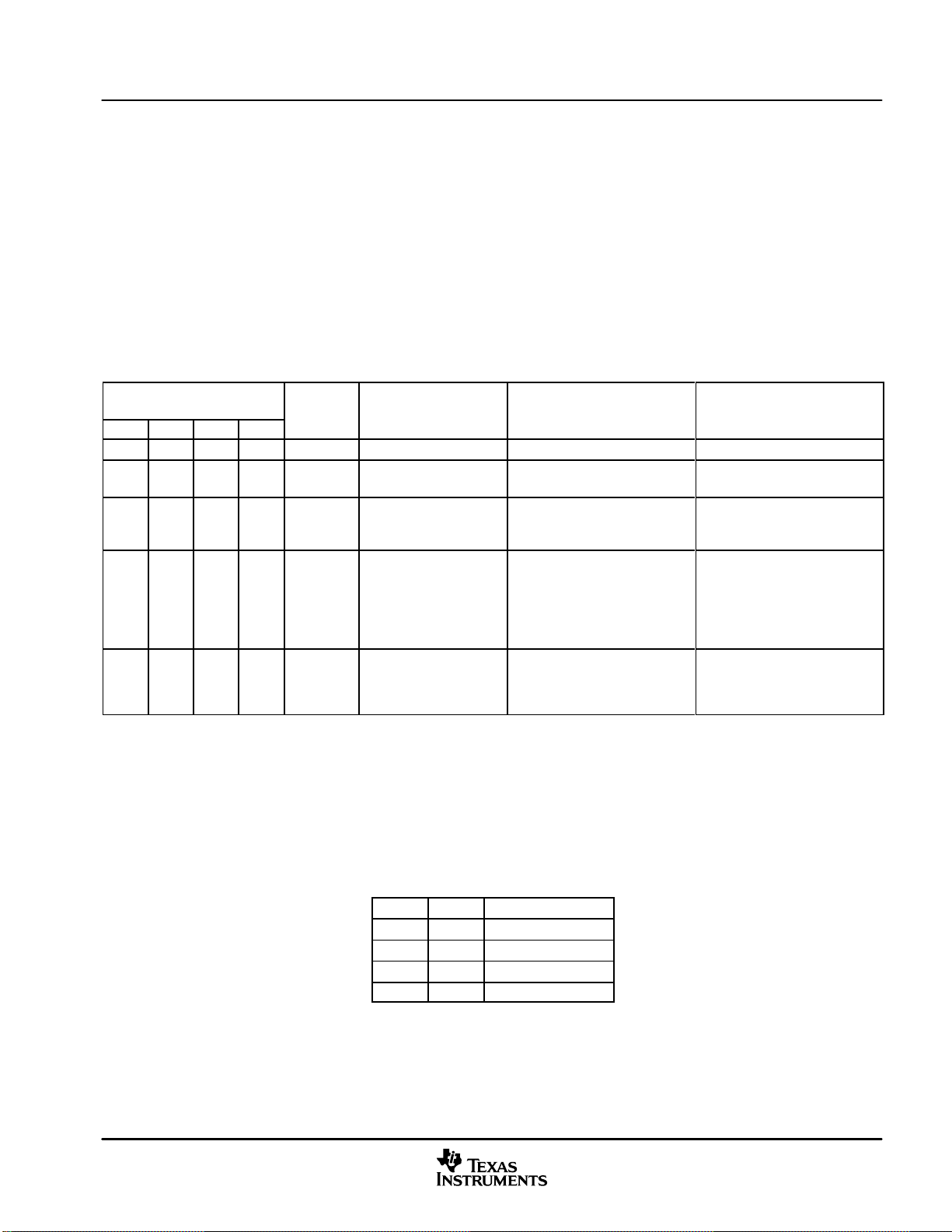
Functional Overview
INTERRUPT TYPE
INTERRUPT SOURCE
When an interrupt is generated, the IIR indicates that an interrupt is pending and encodes the type of interrupt
in its three least significant bits (bits 0, 1, and 2). The contents of this register are summarized in Table 3−15
and described in Table 3−17. Detail on each bit is as follows:
• Bit 0: This bit is used either in a hardwire prioritized or polled interrupt system. When bit 0 is cleared, an
interrupt is pending If bit 0 is set, no interrupt is pending.
• Bits 1 and 2: These two bits identify the highest priority interrupt pending as indicated in Table 3−15
• Bit 3: This bit is always cleared in TL16C450 mode. In FIFO mode, bit 3 is set with bit 2 to indicate that a
time-out interrupt is pending.
• Bits 4 and 5: These two bits are not used (always cleared).
• Bits 6 and 7: These bits are always cleared in TL16C450 mode. They are set when bit 0 of the FIFO control
register is set.
Table 3−17. Interrupt Control Functions
INTERRUPT
IDENTIFICATION REGISTER
BIT 3 BIT 2 BIT 1 BIT 0
0 0 0 1 None None None None
0 1 1 0 1 Receiver line status
0 1 0 0 2 Received data available
1 1 0 0 2
0 0 1 0 3
PRIORITY
LEVEL
INTERRUPT TYPE INTERRUPT SOURCE
Overrun error, parity error,
framing error, or break interrupt
Receiver data available in the
TL16C450 mode or trigger level
reached in the FIFO mode
No characters have been
Character time-out
indication
Transmitter holding
register empty
removed from or input to the
receiver FIFO during the last four
character times, and there is at
least one character in it during
this time
Transmitter holding register
empty
INTERRUPT RESET
METHOD
Read the line status register
Read the receiver buffer register
Read the receiver buffer register
Read the interrupt identification
register (if source of interrupt) or
writing into the transmitter
holding register
3.13.7 Line Control Register (LCR)
The system programmer controls the format of the asynchronous data communication exchange through the
LCR. In addition, the programmer is able to retrieve, inspect, and modify the contents of the LCR; this eliminates
the need for separate storage of the line characteristics in system memory. The contents of this register are
summarized in Table 3−15 and described in the following bulleted list.
• Bits 0 and 1: These two bits specify the number of bits in each transmitted or received serial character.
These bits are encoded as shown in Table 3−18.
Table 3−18. Serial Character Word Length
BIT 1 BIT 0 WORD LENGTH
0 0 5 bits
0 1 6 bits
1 0 7 bits
1 1 8 bits
• Bit 2: This bit specifies either one, one and one-half, or two stop bits in each transmitted character. When
bit 2 is cleared, one stop bit is generated in the data. When bit 2 is set, the number of stop bits generated
is dependent on the word length selected with bits 0 and 1. The receiver clocks only the first stop bit
regardless of the number of stop bits selected. The number of stop bits generated in relation to word length
and bit 2 are shown in Table 3−19.
November 2001 − Revised April 2004 SPRS007D
55
Page 56

Functional Overview
Table 3−19. Number of Stop Bits Generated
BIT 2
WORD LENGTH SELECTED
BY BITS 1 AND 2
0 Any word length 1
1 5 bits 1 1/2
1 6 bits 2
1 7 bits 2
1 8 bits 2
NUMBER OF STOP
BITS GENERATED
• Bit 3: This bit is the parity enable bit. When bit 3 is set, a parity bit is generated in transmitted data between
the last data word bit and the first stop bit. In received data, if bit 3 is set, parity is checked. When bit 3 is
cleared, no parity is generated or checked.
• Bit 4: This bit is the even parity select bit. When parity is enabled (bit 3 is set) and bit 4 is set even parity
(an even number of logic 1s in the data and parity bits) is selected. When parity is enabled and bit 4 is
cleared, odd parity (an odd number of logic 1s) is selected.
• Bit 5: This bit is the stick parity bit. When bits 3, 4, and 5 are set, the parity bit is transmitted and checked
as cleared. When bits 3 and 5 are set and bit 4 is cleared, the parity bit is transmitted and checked as set.
If bit 5 is cleared, stick parity is disabled.
• Bit 6: This bit is the break control bit. Bit 6 is set to force a break condition; i.e., a condition where SOUT
is forced to the spacing (cleared) state. When bit 6 is cleared, the break condition is disabled and has no
affect on the transmitter logic; it only effects SOUT.
• Bit 7: This bit is the divisor latch access bit (DLAB). Bit 7 must be set to access the divisor latches of the
baud generator during a read or write. Bit 7 must be cleared during a read or write to access the receiver
buffer, the THR, or the IER.
3.13.8 Line Status Register (LSR)
†
The LSR provides information to the CPU concerning the status of data transfers. The contents of this register
are summarized in Table 3−15 and described in the following bulleted list.
• Bit 0: This bit is the data ready (DR) indicator for the receiver. DR is set whenever a complete incoming
character has been received and transferred into the RBR or the FIFO. DR is cleared by reading all of the
data in the RBR or the FIFO.
• Bit 1
‡
: This bit is the overrun error (OE) indicator. When OE is set, it indicates that before the character in
the RBR was read, it was overwritten by the next character transferred into the register. OE is cleared every
time the CPU reads the contents of the LSR. If the FIFO mode data continues to fill the FIFO beyond the
trigger level, an overrun error occurs only after the FIFO is full and the next character has been completely
received in the shift register. An overrun error is indicated to the CPU as soon as it happens. The character
in the shift register is overwritten, but it is not transferred to the FIFO.
• Bit 2
‡
: This bit is the parity error (PE) indicator. When PE is set, it indicates that the parity of the received
data character does not match the parity selected in the LCR (bit 4). PE is cleared every time the CPU reads
the contents of the LSR. In the FIFO mode, this error is associated with the particular character in the FIFO
to which it applies. This error is revealed to the CPU when its associated character is at the top of the FIFO.
• Bit 3
‡
: This bit is the framing error (FE) indicator. When FE is set, it indicates that the received character
did not have a valid (set) stop bit. FE is cleared every time the CPU reads the contents of the LSR. In the
FIFO mode, this error is associated with the particular character in the FIFO to which it applies. This error
is revealed to the CPU when its associated character is at the top of the FIFO. The UART tries to
resynchronize after a framing error. To accomplish this, it is assumed that the framing error is due to the next
start bit. The UART samples this start bit twice and then accepts the input data.
†
The line status register is intended for read operations only; writing to this register is not recommended.
‡
Bits 1 through 4 are the error conditions that produce a receiver line status interrupt.
56
November 2001 − Revised April 2004SPRS007D
Page 57

Functional Overview
• Bit 4‡: This bit is the break interrupt (BI) indicator. When BI is set, it indicates that the received data input
was held low for longer than a full-word transmission time. A full-word transmission time is defined as the
total time to transmit the start, data, parity, and stop bits. BI is cleared every time the CPU reads the contents
of the LSR. In the FIFO mode, this error is associated with the particular character in the FIFO to which it
applies. This error is revealed to the CPU when its associated character is at the top of the FIFO. When a
break occurs, only one 0 character is loaded into the FIFO. The next character transfer is enabled after SIN
goes to the marking state for at least two RCLK samples and then receives the next valid start bit.
• Bit 5: This bit is the THRE indicator. THRE is set when the THR is empty, indicating that the UART is ready
to accept a new character. If the THRE interrupt is enabled when THRE is set, an interrupt is generated.
THRE is set when the contents of the THR are transferred to the TSR. THRE is cleared concurrent with the
loading of the THR by the CPU. In the FIFO mode, THRE is set when the transmit FIFO is empty; it is cleared
when at least one byte is written to the transmit FIFO.
• Bit 6: This bit is the transmitter empty (TEMT) indicator. TEMT bit is set when the THR and the TSR are
both empty. When either the THR or the TSR contains a data character, TEMT is cleared. In the FIFO mode,
TEMT is set when the transmitter FIFO and shift register are both empty.
• Bit 7: In the TL16C550C mode, this bit is always cleared. In the TL16C450 mode, this bit is always cleared.
In the FIFO mode, LSR7 is set when there is at least one parity, framing, or break error in the FIFO. It is
cleared when the microprocessor reads the LSR and there are no subsequent errors in the FIFO.
3.13.9 Modem Control Register (MCR)
The MCR is an 8-bit register that controls an interface with a modem, data set, or peripheral device. On the UART
peripheral, only one bit is active in this register
• Bit 4: This bit (LOOP) provides a local loop back feature for diagnostic testing of the UART. When LOOP
is set, the following occurs:
− The transmitter SOUT is set high.
− The receiver SIN is disconnected.
− The output of the TSR is looped back into the receiver shift register input.
3.13.10 Programmable Baud Generator
The UART contains a programmable baud generator that takes a clock input in the range between DC and
16 MHz and divides it by a divisor in the range between 1 and (2
generator is sixteen times (16×) the baud rate. The formula for the divisor is:
divisor = XIN frequency input ÷ (desired baud rate × 16)
Two 8-bit registers, called divisor latches, store the divisor in a 16-bit binary format. These divisor latches must
be loaded during initialization of the UART in order to ensure desired operation of the baud generator. When
either of the divisor latches is loaded, a 16-bit baud counter is also loaded to prevent long counts on initial load.
Table 3−20 and Table 3−21 illustrate the use of the baud generator with clock frequencies of 1.8432 MHz and
3.072 MHz respectively. For baud rates of 38.4 kbits/s and below, the error obtained is very small. The accuracy
of the selected baud rate is dependent on the selected clock frequency.
16
−1). The output frequency of the baud
‡
Bits 1 through 4 are the error conditions that produce a receiver line status interrupt.
November 2001 − Revised April 2004 SPRS007D
57
Page 58
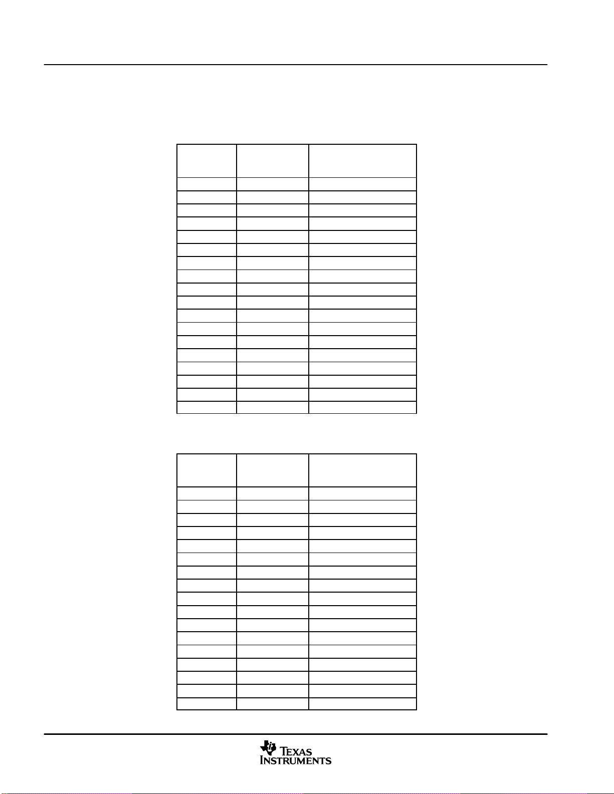
Functional Overview
NOTE: The clock rates in Table 3−20 and Table 3−21 are shown, for example only, to illustrate
the relationship of clock rate and divisor value, to baud rate and baud rate error. Typically,
higher clock rates will normally be used, and error values will differ accordingly.
Table 3−20. Baud Rates Using a 1.8432-MHz Clock
DESIRED
BAUD RATE
50 2304
75 1536
110 1047 0.026
134.5 857 0.058
150 768
300 384
600 192
1200 96
1800 64
2000 58 0.69
2400 48
3600 32
4800 24
7200 16
9600 12
19200 6
38400 3
56000 2 2.86
DIVISOR USED
TO GENERATE
16 × CLOCK
PERCENT ERROR
DIFFERENCE BETWEEN
DESIRED AND ACTUAL
Table 3−21. Baud Rates Using a 3.072-MHz Clock
DESIRED
BAUD RATE
50 3840
75 2560
110 1745 0.026
134.5 1428 0.034
150 1280
300 640
600 320
1200 160
1800 107 0.312
2000 96
2400 80
3600 53 0.628
4800 40
7200 27 1.23
9600 20
19200 10
38400 5
DIVISOR USED
TO GENERATE
16 × CLOCK
PERCENT ERROR
DIFFERENCE BETWEEN
DESIRED AND ACTUAL
58
November 2001 − Revised April 2004SPRS007D
Page 59

Functional Overview
3.13.10.1 Receiver Buffer Register (RBR)
The UART receiver section consists of a receiver shift register (RSR) and a RBR. The RBR is actually a 16-byte
FIFO. Timing is supplied by the 16× receiver clock. Receiver section control is a function of the UART line control
register.
The UART RSR receives serial data from SIN. The RSR then concatenates the data and moves it into the RBR
FIFO. In the TL16C450 mode, when a character is placed in the RBR and the received data available interrupt
is enabled (IER0 = 1), an interrupt is generated. This interrupt is cleared when the data is read out of the RBR.
In the FIFO mode, the interrupts are generated based on the control setup in the FIFO control register.
3.13.10.2 Scratch Register
The scratch register is an 8-bit register that is intended for the programmer’s use as a scratchpad in the sense
that it temporarily holds the programmer’s data without affecting any other UART operation.
3.13.10.3 Transmitter Holding Register (THR)
The UART transmitter section consists of a THR and a transmitter shift register (TSR). The THR is actually a
16-byte FIFO. Transmitter section control is a function of the UART line control register.
The UART THR receives data off the internal data bus and when the shift register is idle, moves it into the TSR.
The TSR serializes the data and outputs it at SOUT. In the TL16C450 mode, if the THR is empty and the
transmitter holding register empty (THRE) interrupt is enabled (IER1 = 1), an interrupt is generated. This
interrupt is cleared when a character is loaded into the register. In the FIFO mode, the interrupts are generated
based on the control setup in the FIFO control register.
3.14 General-Purpose I/O Pins
In addition to the standard BIO and XF pins, the 5407/5404 has pins that can be configured for
general-purpose I/O. These pins are:
• 16 McBSP pins — BCLKX0/1, BCLKR0/1, BDR0/1/2, BFSX0/1, BFSR0/1, BDX0/1/2, BCLKRX2,
BFSRX2
• 8 HPI data pins — HD0−HD7
The general-purpose I/O function of these pins is only available when the primary pin function is not required.
3.14.1 McBSP Pins as General-Purpose I/O
When the receive or transmit portion of a McBSP is in reset, its pins can be configured as general-purpose
inputs or outputs. For more details on this feature, see Section 3.8.
3.14.2 HPI Data Pins as General-Purpose I/O
The 8-bit bidirectional data bus of the HPI can be used as general-purpose input/output (GPIO) pins when the
HPI is disabled (HPIENA = 0) or when the HPI is used in HPI16 mode (HPI16 = 1). Two memory-mapped
registers are used to control the GPIO function of the HPI data pins — the general-purpose I/O control register
(GPIOCR) and the general-purpose I/O status register (GPIOSR). The GPIOCR is shown in Figure 3−23.
15
TOUT1 Reserved
R/W-0 0
7
DIR7
R/W-0 R/W-0 R/W-0 R/W-0 R/W-0 R/W-0 R/W-0 R/W-0
LEGEND: R = Read, W = Write, n = value after reset
Figure 3−23. General-Purpose I/O Control Register (GPIOCR) [MMR Address 003Ch]
14 8
43 0
DIR6 DIR5 DIR4 DIR3 DIR2 DIR1 DIR0
November 2001 − Revised April 2004 SPRS007D
59
Page 60

Functional Overview
The direction bits (DIRx) are used to configure HD0−HD7 as inputs or outputs (0 = input, 1 = output).
Bit 15 of the GPIOCR is also used as the Timer1 output enable bit, TOUT1. The TOUT1 bit enables or disables
the Timer1 output on the HINT
TOUT1 = 1, the Timer1 output is driven on the HINT
available when the HPI is disabled (HPIENA input pin = 0).
The status of the GPIO pins can be monitored using the bits of the GPIOSR. The GPIOSR is shown in
Figure 3−24. When read, these bits reflect the state of the input pins, and when written, determine the state
of outputs.
/TOUT1 pin. If TOUT1 = 0, the Timer1 output is not available externally; if
/TOUT1 pin. Note also that the Timer1 output is only
15
Reserved
0
7
IO7
R/W-0 R/W-0 R/W-0 R/W-0 R/W-0 R/W-0 R/W-0 R/W-0
LEGEND: R = Read, W = Write, n = value after reset
IO6 IO5 IO4 IO3 IO2 IO1 IO0
43 0
Figure 3−24. General-Purpose I/O Status Register (GPIOSR) [MMR Address 003Dh]
3.15 Device ID Register
A read-only memory-mapped register has been added to the 5407/5404 to allow user application software
to identify on which device the program is being executed.
15
Chip ID
R
8
8
7
Chip Revision
RR
LEGEND: R = Read, W = Write
43 0
Figure 3−25. Device ID Register (CSIDR) [MMR Address 003Eh]
Table 3−22. Device ID Register (CSIDR) Bit Functions
BIT
NO.
15−8 Chip ID Chip identification (hex code of 06 for 5407 and 03 for 5404)
7−4 Chip Revision Chip revision identification
3−0 SUBSYSID Subsystem identification (0000b for single core devices)
60
BIT
NAME
FUNCTION
SUBSYSID
November 2001 − Revised April 2004SPRS007D
Page 61

3.16 Memory-Mapped Registers
The 5407/5404 has 27 memory-mapped CPU registers, which are mapped in data memory space address
0h to 1Fh. Each 5407/5404 device also has a set of memory-mapped registers associated with peripherals.
Table 3−23 gives a list of CPU memory-mapped registers (MMRs) available on 5407/5404. Table 3−24 shows
additional peripheral MMRs associated with the 5407/5404.
Table 3−23. CPU Memory-Mapped Registers
Functional Overview
NAME
IMR 0 0 Interrupt mask register
IFR 1 1 Interrupt flag register
— 2−5 2−5 Reserved for testing
ST0 6 6 Status register 0
ST1 7 7 Status register 1
AL 8 8 Accumulator A low word (15−0)
AH 9 9 Accumulator A high word (31−16)
AG 10 A Accumulator A guard bits (39−32)
BL 11 B Accumulator B low word (15−0)
BH 12 C Accumulator B high word (31−16)
BG 13 D Accumulator B guard bits (39−32)
TREG 14 E Temporary register
TRN 15 F Transition register
AR0 16 10 Auxiliary register 0
AR1 17 11 Auxiliary register 1
AR2 18 12 Auxiliary register 2
AR3 19 13 Auxiliary register 3
AR4 20 14 Auxiliary register 4
AR5 21 15 Auxiliary register 5
AR6 22 16 Auxiliary register 6
AR7 23 17 Auxiliary register 7
SP 24 18 Stack pointer register
BK 25 19 Circular buffer size register
BRC 26 1A Block repeat counter
RSA 27 1B Block repeat start address
REA 28 1C Block repeat end address
PMST 29 1D Processor mode status (PMST) register
XPC 30 1E Extended program page register
— 31 1F Reserved
ADDRESS
DEC HEX
DESCRIPTION
November 2001 − Revised April 2004 SPRS007D
61
Page 62
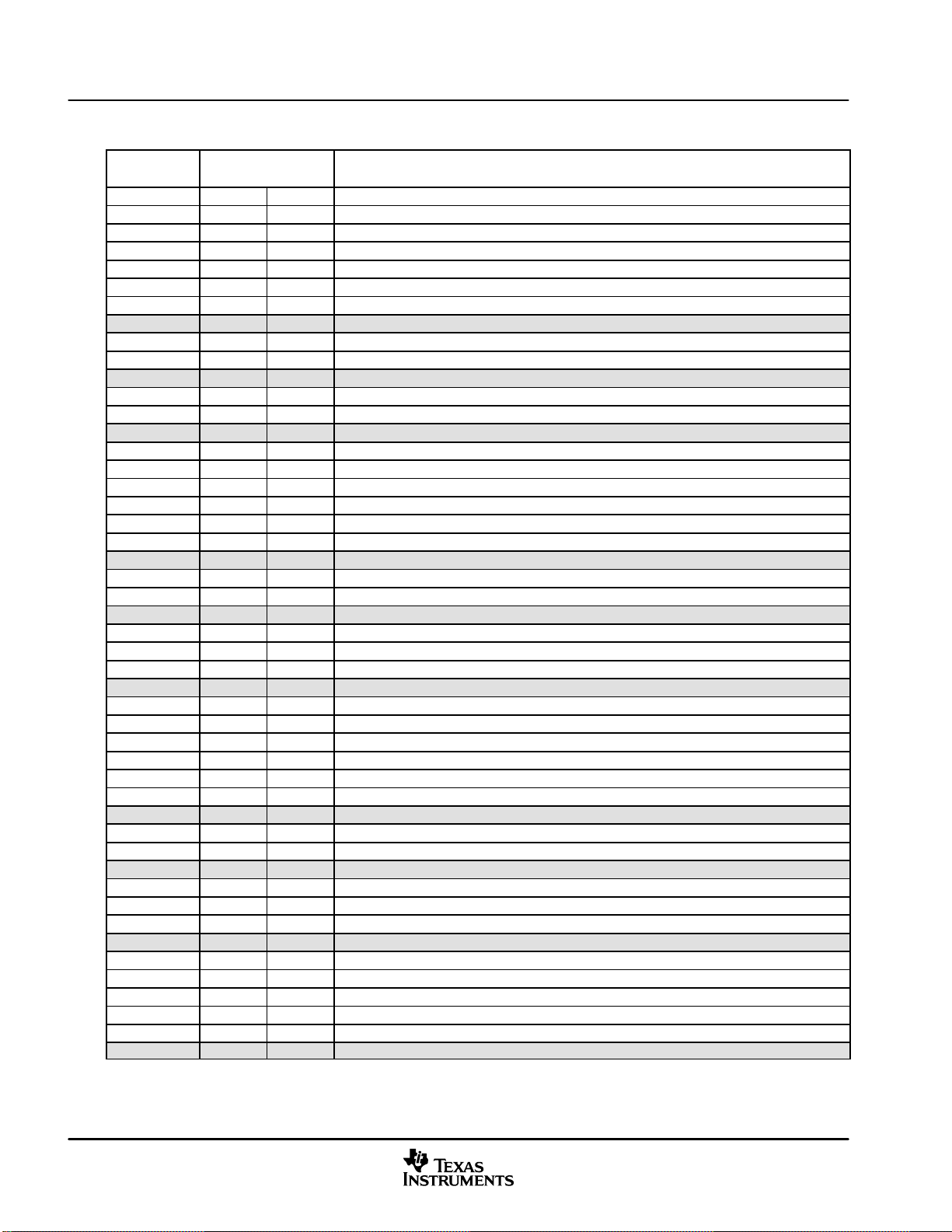
Functional Overview
NAME
DESCRIPTION
Table 3−24. Peripheral Memory-Mapped Registers for Each DSP Subsystem
ADDRESS
DEC HEX
DRR20 32 20 McBSP 0 Data Receive Register 2
DRR10 33 21 McBSP 0 Data Receive Register 1
DXR20 34 22 McBSP 0 Data Transmit Register 2
DXR10 35 23 McBSP 0 Data Transmit Register 1
TIM 36 24 Timer 0 Register
PRD 37 25 Timer 0 Period Register
TCR 38 26 Timer 0 Control Register
— 39 27 Reserved
SWWSR 40 28 Software Wait-State Register
BSCR 41 29 Bank-Switching Control Register
— 42 2A Reserved
SWCR 43 2B Software Wait-State Control Register
HPIC 44 2C HPI Control Register (HMODE = 0 only)
— 45−47 2D−2F Reserved
DRR22 48 30 McBSP 2 Data Receive Register 2
DRR12 49 31 McBSP 2 Data Receive Register 1
DXR22 50 32 McBSP 2 Data Transmit Register 2
DXR12 51 33 McBSP 2 Data Transmit Register 1
SPSA2 52 34 McBSP 2 Subbank Address Register
SPSD2 53 35 McBSP 2 Subbank Data Register
— 54−55 36−37 Reserved
SPSA0 56 38 McBSP 0 Subbank Address Register
SPSD0 57 39 McBSP 0 Subbank Data Register
— 58−59 3A−3B Reserved
GPIOCR 60 3C General-Purpose I/O Control Register
GPIOSR 61 3D General-Purpose I/O Status Register
CSIDR 62 3E Device ID Register
— 63 3F Reserved
DRR21 64 40 McBSP 1 Data Receive Register 2
DRR11 65 41 McBSP 1 Data Receive Register 1
DXR21 66 42 McBSP 1 Data Transmit Register 2
DXR11 67 43 McBSP 1 Data Transmit Register 1
USAR 68 44 UART Subbank Address Register
USDR 69 45 UART Subbank Data Register
— 70−71 46−47 Reserved
SPSA1 72 48 McBSP 1 Subbank Address Register
SPSD1 73 49 McBSP 1 Subbank Data Register
— 74−75 4A−4B Reserved
TIM1 76 4C Timer 1 Register
PRD1 77 4D Timer 1 Period Register
TCR1 78 4E Timer 1 Control Register
— 79−83 4F−53 Reserved
DMPREC 84 54 DMA Priority and Enable Control Register
DMSA 85 55 DMA Subbank Address Register
DMSDI 86 56 DMA Subbank Data Register with Autoincrement
DMSDN 87 57 DMA Subbank Data Register
CLKMD 88 58 Clock Mode Register (CLKMD)
— 89−95 59−5F Reserved
†
See Table 3−25 for a detailed description of the McBSP control registers and their subaddresses.
‡
See Table 3−26 for a detailed description of the DMA subbank addressed registers.
‡
†
†
†
†
†
†
‡
‡
62
November 2001 − Revised April 2004SPRS007D
Page 63

3.17 McBSP Control Registers and Subaddresses
SUB-
Á
Á
Á
Á
Á
Á
Á
Á
Á
Á
Á
Á
Á
Á
Á
Á
Á
Á
Á
Á
Á
Á
Á
Á
Á
Á
Á
Á
Á
Á
Á
Á
Á
Á
Á
Á
Á
Á
Á
Á
Á
Á
Á
Á
Á
Á
Á
Á
The control registers for the multichannel buffered serial port (McBSP) are accessed using the subbank
addressing scheme. This allows a set or subbank of registers to be accessed through a single memory
location. The McBSP subbank address register (SPSA) is used as a pointer to select a particular register within
the subbank. The McBSP data register (SPSDx) is used to access (read or write) the selected register.
Table 3−25 shows the McBSP control registers and their corresponding subaddresses.
Table 3−25. McBSP Control Registers and Subaddresses
McBSP0 McBSP1 McBSP2
NAME ADDRESS NAME ADDRESS NAME ADDRESS
SPCR10
SPCR20
RCR10
RCR20
XCR10
XCR20
SRGR10
SRGR20
MCR10
MCR20
RCERA0
RCERB0
XCERA0
XCERB0
PCR0
RCERC0
ÁÁ
RCERD0
XCERC0
ÁÁ
XCERD0
RCERE0
ÁÁ
RCERF0
XCERE0
XCERF0
ÁÁ
RCERG0
RCERH0
ÁÁ
XCERG0
XCERH0
ÁÁ
39h
39h
39h
39h
39h
39h
39h
39h
39h
39h
39h
39h
39h
39h
39h
39h
ÁÁ
39h
39h
ÁÁ
39h
39h
ÁÁ
39h
39h
39h
ÁÁ
39h
39h
ÁÁ
39h
39h
ÁÁ
SPCR11
SPCR21
RCR11
RCR21
XCR11
XCR21
SRGR11
SRGR21
MCR11
MCR21
RCERA1
RCERB1
XCERA1
XCERB1
PCR1
RCERC1
ÁÁ
RCERD1
XCERC1
ÁÁ
XCERD1
RCERE1
ÁÁ
RCERF1
XCERE1
XCERF1
ÁÁ
RCERG1
RCERH1
ÁÁ
XCERG1
XCERH1
ÁÁ
49h
49h
49h
49h
49h
49h
49h
49h
49h
49h
49h
49h
49h
49h
49h
49h
ÁÁ
49h
49h
ÁÁ
49h
49h
ÁÁ
49h
49h
49h
ÁÁ
49h
49h
ÁÁ
49h
49h
ÁÁ
SPCR12
SPCR22
RCR12
RCR22
XCR12
XCR22
SRGR12
SRGR22
MCR12
MCR22
RCERA2
RCERA2
XCERA2
XCERA2
PCR2
RCERC2
ÁÁ
RCERD2
XCERC2
ÁÁ
XCERD2
RCERE2
ÁÁ
RCERF2
XCERE2
XCERF2
ÁÁ
RCERG2
RCERH2
ÁÁ
XCERG2
XCERH2
ÁÁ
35h
35h
35h
35h
35h
35h
35h
35h
35h
35h
35h
35h
35h
35h
35h
35h
ÁÁ
35h
35h
ÁÁ
35h
35h
ÁÁ
35h
35h
35h
ÁÁ
35h
35h
ÁÁ
35h
35h
ÁÁ
SUB-
ADDRESS
00h
01h
02h
03h
04h
05h
06h
07h
08h
09h
0Ah
0Bh
0Ch
0Dh
0Eh
010h
ÁÁÁ
011h
012h
ÁÁÁ
013h
014h
ÁÁÁ
015h
016h
017h
ÁÁÁ
018h
019h
ÁÁÁ
01Ah
01Bh
ÁÁÁ
Functional Overview
DESCRIPTION
Serial port control register 1
Serial port control register 2
Receive control register 1
Receive control register 2
Transmit control register 1
Transmit control register 2
Sample rate generator register 1
Sample rate generator register 2
Multichannel register 1
Multichannel register 2
Receive channel enable register partition A
Receive channel enable register partition B
Transmit channel enable register partition A
Transmit channel enable register partition B
Pin control register
Additional channel enable register for
128-channel selection
ББББББББББ
Additional channel enable register for
128-channel selection
Additional channel enable register for
128-channel selection
ББББББББББ
Additional channel enable register for
128-channel selection
Additional channel enable register for
128-channel selection
ББББББББББ
Additional channel enable register for
128-channel selection
Additional channel enable register for
128-channel selection
Additional channel enable register for
ББББББББББ
128-channel selection
Additional channel enable register for
128-channel selection
Additional channel enable register for
128-channel selection
ББББББББББ
Additional channel enable register for
128-channel selection
Additional channel enable register for
128-channel selection
ББББББББББ
November 2001 − Revised April 2004 SPRS007D
63
Page 64
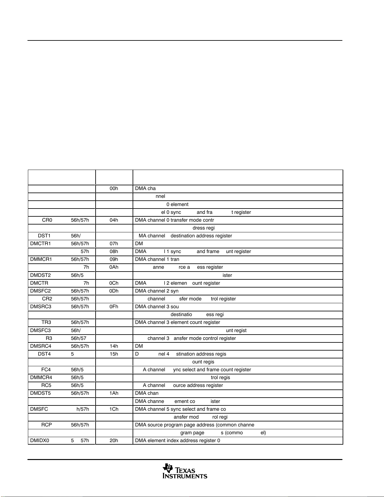
Functional Overview
3.18 DMA Subbank Addressed Registers
The direct memory access (DMA) controller has several control registers associated with it. The main control
register (DMPREC) is a standard memory-mapped register. However, the other registers are accessed using
the subbank addressing scheme. This allows a set or subbank of registers to be accessed through a single
memory location. The DMA subbank address (DMSA) register is used as a pointer to select a particular
register within the subbank, while the DMA subbank data (DMSD) register or the DMA subbank data register
with autoincrement (DMSDI) is used to access (read or write) the selected register.
When the DMSDI register is used to access the subbank, the subbank address is automatically
postincremented so that a subsequent access affects the next register within the subbank. This autoincrement
feature is intended for efficient, successive accesses to several control registers. If the autoincrement feature
is not required, the DMSDN register should be used to access the subbank. Table 3−26 shows the DMA
controller subbank addressed registers and their corresponding subaddresses.
Table 3−26. DMA Subbank Addressed Registers
NAME ADDRESS
DMSRC0 56h/57h
DMDST0 56h/57h
DMCTR0 56h/57h
DMSFC0
DMMCR0
DMSRC1
DMDST1
DMCTR1
DMSFC1
DMMCR1
DMSRC2
DMDST2
DMCTR2
DMSFC2
DMMCR2
DMSRC3
DMDST3
DMCTR3
DMSFC3
DMMCR3
DMSRC4
DMDST4
DMCTR4
DMSFC4
DMMCR4
DMSRC5
DMDST5
DMCTR5
DMSFC5
DMMCR5
DMSRCP
DMDSTP
DMIDX0
56h/57h
56h/57h
56h/57h
56h/57h
56h/57h
56h/57h
56h/57h
56h/57h
56h/57h
56h/57h
56h/57h
56h/57h
56h/57h
56h/57h
56h/57h
56h/57h
56h/57h
56h/57h
56h/57h
56h/57h
56h/57h
56h/57h
56h/57h
56h/57h
56h/57h
56h/57h
56h/57h
56h/57h
56h/57h
56h/57h
SUB-
ADDRESS
00h DMA channel 0 source address register
01h DMA channel 0 destination address register
02h DMA channel 0 element count register
03h
04h
05h
06h
07h
08h
09h
0Ah
0Bh
0Ch
0Dh
0Eh
0Fh
10h
11h
12h
13h
14h
15h
16h
17h
18h
19h
1Ah
1Bh
1Ch
1Dh
1Eh
1Fh
20h
DMA channel 0 sync select and frame count register
DMA channel 0 transfer mode control register
DMA channel 1 source address register
DMA channel 1 destination address register
DMA channel 1 element count register
DMA channel 1 sync select and frame count register
DMA channel 1 transfer mode control register
DMA channel 2 source address register
DMA channel 2 destination address register
DMA channel 2 element count register
DMA channel 2 sync select and frame count register
DMA channel 2 transfer mode control register
DMA channel 3 source address register
DMA channel 3 destination address register
DMA channel 3 element count register
DMA channel 3 sync select and frame count register
DMA channel 3 transfer mode control register
DMA channel 4 source address register
DMA channel 4 destination address register
DMA channel 4 element count register
DMA channel 4 sync select and frame count register
DMA channel 4 transfer mode control register
DMA channel 5 source address register
DMA channel 5 destination address register
DMA channel 5 element count register
DMA channel 5 sync select and frame count register
DMA channel 5 transfer mode control register
DMA source program page address (common channel)
DMA destination program page address (common channel)
DMA element index address register 0
DESCRIPTION
64
November 2001 − Revised April 2004SPRS007D
Page 65

Table 3−26. DMA Subbank Addressed Registers (Continued)
NAME DESCRIPTION
DMIDX1
DMFRI0
DMFRI1
DMGSA0
DMGDA0
DMGCR0
DMGFR0
XSRCDP
XDSTDP
DMGSA1
DMGDA1
DMGCR1
DMGFR1
DMGSA2
DMGDA2
DMGCR2
DMGFR2
DMGSA3
DMGDA3
DMGCR3
DMGFR3
DMGSA4
DMGDA4
DMGCR4
DMGFR4
DMGSA5
DMGDA5
DMGCR5
DMGFR5
ADDRESS
56h/57h
56h/57h
56h/57h
56h/57h
56h/57h
56h/57h
56h/57h
56h/57h
56h/57h
56h/57h
56h/57h
56h/57h
56h/57h
56h/57h
56h/57h
56h/57h
56h/57h
56h/57h
56h/57h
56h/57h
56h/57h
56h/57h
56h/57h
56h/57h
56h/57h
56h/57h
56h/57h
56h/57h
56h/57h
SUB-
ADDRESS
21h
22h
23h
24h
25h
26h
27h
28h
29h
2Ah
2Bh
2Ch
2Dh
2Eh
2Fh
30h
31h
32h
33h
34h
35h
36h
37h
38h
39h
3Ah
3Bh
3Ch
3Dh
DMA element index address register 1
DMA frame index register 0
DMA frame index register 1
DMA global source address reload register, channel 0
DMA global destination address reload register, channel 0
DMA global count reload register, channel 0
DMA global frame count reload register, channel 0
DMA extended source data page
DMA extended destination data page
DMA global source address reload register, channel 1
DMA global destination address reload register, channel 1
DMA global count reload register, channel 1
DMA global frame count reload register, channel 1
DMA global source address reload register, channel 2
DMA global destination address reload register, channel 2
DMA global count reload register, channel 2
DMA global frame count reload register, channel 2
DMA global source address reload register, channel 3
DMA global destination address reload register, channel 3
DMA global count reload register, channel 3
DMA global frame count reload register, channel 3
DMA global source address reload register, channel 4
DMA global destination address reload register, channel 4
DMA global count reload register, channel 4
DMA global frame count reload register, channel 4
DMA global source address reload register, channel 5
DMA global destination address reload register, channel 5
DMA global count reload register, channel 5
DMA global frame count reload register, channel 5
Functional Overview
November 2001 − Revised April 2004 SPRS007D
65
Page 66

Functional Overview
3.19 Interrupts
Vector-relative locations and priorities for all internal and external interrupts are shown in Table 3−27.
Table 3−27. Interrupt Locations and Priorities
NAME
RS, SINTR 0 00 1 Reset (hardware and software reset)
NMI, SINT16 4 04 2 Nonmaskable interrupt
SINT17 8 08 — Software interrupt #17
SINT18 12 0C — Software interrupt #18
SINT19 16 10 — Software interrupt #19
SINT20 20 14 — Software interrupt #20
SINT21 24 18 — Software interrupt #21
SINT22 28 1C — Software interrupt #22
SINT23 32 20 — Software interrupt #23
SINT24 36 24 — Software interrupt #24
SINT25 40 28 — Software interrupt #25
SINT26 44 2C — Software interrupt #26
SINT27 48 30 — Software interrupt #27
SINT28 52 34 — Software interrupt #28
SINT29 56 38 — Software interrupt #29
SINT30 60 3C — Software interrupt #30
INT0, SINT0 64 40 3 External user interrupt #0
INT1, SINT1 68 44 4 External user interrupt #1
INT2, SINT2 72 48 5 External user interrupt #2
TINT0, SINT3 76 4C 6 Timer 0 interrupt
BRINT0, SINT4 80 50 7 McBSP #0 receive interrupt
BXINT0, SINT5 84 54 8 McBSP #0 transmit interrupt
BRINT2, SINT6 88 58 9 McBSP #2 receive interrupt (default)
BXINT2, SINT7 92 5C 10 McBSP #2 transmit interrupt (default)
INT3, TINT1, SINT8 96 60 11 External user interrupt #3/Timer 1 interrupt
HINT, SINT9 100 64 12 HPI interrupt
BRINT1, SINT10 104 68 13 McBSP #1 receive interrupt (default)
BXINT1, SINT11 108 6C 14 McBSP #1 transmit interrupt (default)
DMAC4,SINT12 11 2 70 15 DMA channel 4
DMAC5,SINT13 11 6 74 16 DMA channel 5
UART, SINT14 120 78 — UART interrupt
Reserved 124−127 7C−7F — Reserved
†
See Table 3−13 for other interrupt selections.
‡
The INT3 and TINT1 interrupts are ORed together. To distinguish one from the other, one of these two interrupt sources must be inhibited.
LOCATION
DECIMAL HEX
PRIORITY FUNCTION
†
†
†
†
‡
66
November 2001 − Revised April 2004SPRS007D
Page 67

3.19.1 IFR and IMR Registers
The bit layout of the interrupt flag register (IFR) and the interrupt mask register (IMR) is shown in Figure 3−26.
Functional Overview
15
Reserved UART DMAC5 DMAC4 BXINT1 BRINT1 HINT INT3
7
BXINT2
†
Bit 8 reflects the status of either INT3 or TINT1: these two interrupts are ORed together. To distinguish one from the other, one of these two interrupt
sources must be inhibited.
14 13 12 11 10 9 8
†
654321 0
BRINT2 BXINT0 BRINT0 TINT0 INT2 INT1 INT0
Figure 3−26. IFR and IMR
November 2001 − Revised April 2004 SPRS007D
67
Page 68

Documentation Support
4 Documentation Support
Extensive documentation supports all TMS320 DSP family of devices from product announcement through
applications development. The following types of documentation are available to support the design and use
of the C5000 platform of DSPs:
• TMS320C54x DSP Functional Overview (literature number SPRU307)
• Device-specific data sheets
• Complete user’s guides
• Development support tools
• Hardware and software application reports
The five-volume TMS320C54x DSP Reference Set (literature number SPRU210) consists of:
• Volume 1: CPU and Peripherals (literature number SPRU131)
• Volume 2: Mnemonic Instruction Set (literature number SPRU172)
• Volume 3: Algebraic Instruction Set (literature number SPRU179)
• Volume 4: Applications Guide (literature number SPRU173)
• Volume 5: Enhanced Peripherals (literature number SPRU302)
The reference set describes in detail the TMS320C54x DSP products currently available and the hardware
and software applications, including algorithms, for fixed-point TMS320 DSP family of devices.
A series of DSP textbooks is published by Prentice-Hall and John Wiley & Sons to support digital signal
processing research and education. The TMS320 DSP newsletter, Details on Signal Processing, is
published quarterly and distributed to update TMS320 DSP customers on product information.
Information regarding TI DSP products is also available on the Worldwide Web at http://www.ti.com uniform
resource locator (URL).
TMS320 and C5000 are trademarks of Texas Instruments.
68
November 2001 − Revised April 2004SPRS007D
Page 69

4.1 Device and Development-Support Tool Nomenclature
To designate the stages in the product development cycle, TI assigns prefixes to the part numbers of all
TMS320 DSP devices and support tools. Each TMS320 DSP commercial family member has one of three
prefixes: TMX, TMP, or TMS (e.g., TMS320VC5407/TMS320VC5404). Texas Instruments recommends two
of three possible prefix designators for support tools: TMDX and TMDS. These prefixes represent evolutionary
stages of product development from engineering prototypes (TMX/ TMDX) through fully qualified production
devices/tools (TMS/TMDS).
Device development evolutionary flow:
TMX Experimental device that is not necessarily representative of the final device’s electrical specifications
TMP Final silicon die that conforms to the device’s electrical specifications but has not completed quality
and reliability verification
TMS Fully qualified production device
Support tool development evolutionary flow:
TMDX Development-support product that has not yet completed Texas Instruments internal qualification
testing.
TMDS Fully qualified development-support product
Documentation Support
TMX and TMP devices and TMDX development-support tools are shipped against the following disclaimer:
“Developmental product is intended for internal evaluation purposes.”
TMS devices and TMDS development-support tools have been characterized fully, and the quality and
reliability of the device have been demonstrated fully. TI’s standard warranty applies.
Predictions show that prototype devices (TMX or TMP) have a greater failure rate than the standard
production devices. Texas Instruments recommends that these devices not be used in any production system
because their expected end-use failure rate still is undefined. Only qualified production devices are to be used.
TMS320 is a trademark of Texas Instruments.
November 2001 − Revised April 2004 SPRS007D
69
Page 70
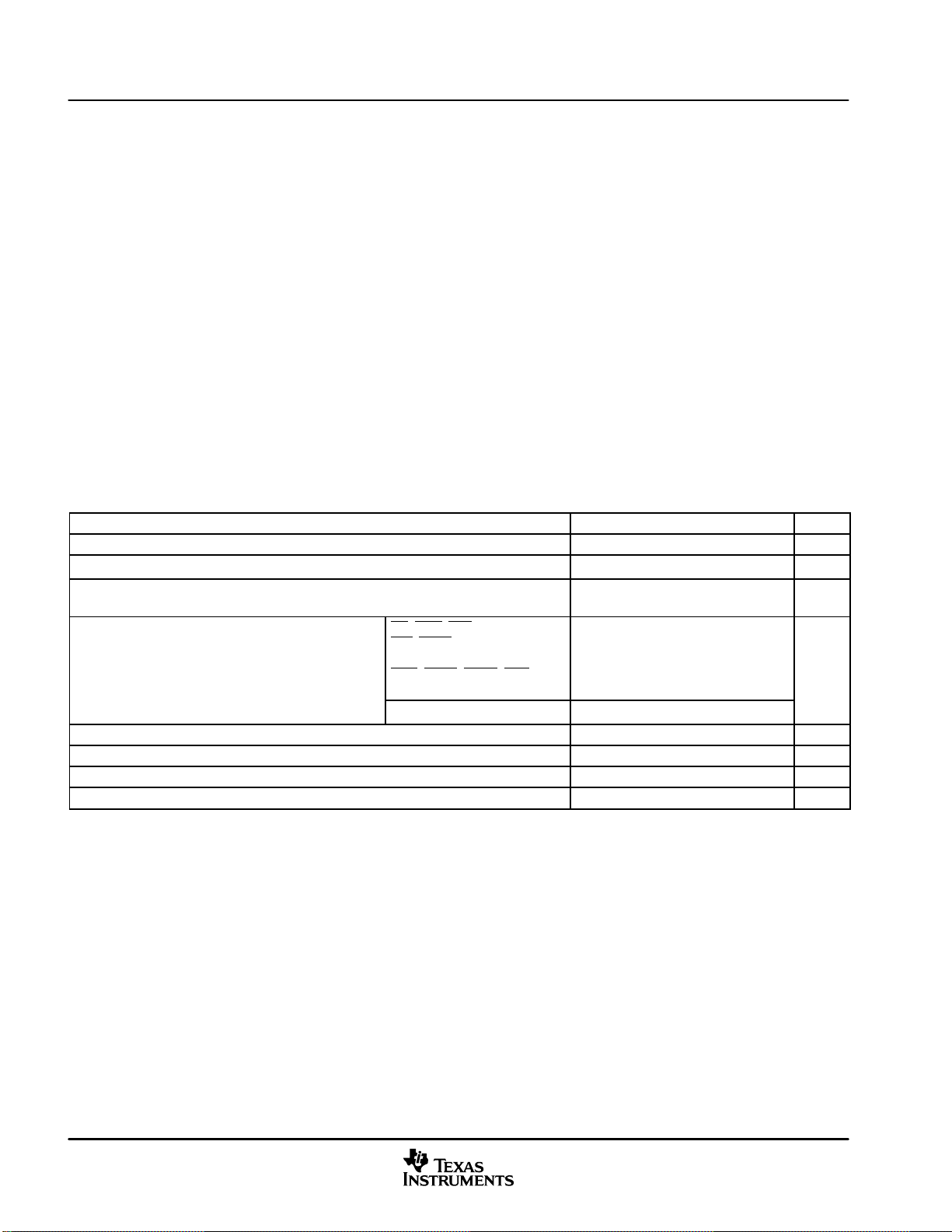
Electrical Specifications
5 Electrical Specifications
This section provides the absolute maximum ratings and the recommended operating conditions for the
TMS320VC5407/TMS320VC5404 DSP.
5.1 Absolute Maximum Ratings
The list of absolute maximum ratings are specified over operating case temperature. Stresses beyond those
listed under “absolute maximum ratings” may cause permanent damage to the device. These are stress
ratings only, and functional operation of the device at these or any other conditions beyond those indicated
under Section 5.2 is not implied. Exposure to absolute-maximum-rated conditions for extended periods may
affect device reliability. All voltage values are with respect to DV
values for a 3.3-V device.
. Figure 5−1 provides the test load circuit
SS
Supply voltage I/O range, DV
Supply voltage core range, CV
DD
DD
Input voltage range −0.3 V to 4.5 V. . . . . . . . . . . . . . . . . . . . . . . . . . . . . . . . . . . . . . . . . . . . . . . . . . . . . . . . . . . . . .
Output voltage range −0.3 V to 4.5 V. . . . . . . . . . . . . . . . . . . . . . . . . . . . . . . . . . . . . . . . . . . . . . . . . . . . . . . . . . . . .
Operating case temperature range, T
Storage temperature range, T
stg
C
5.2 Recommended Operating Conditions
DV
CV
DVSS,
CV
V
IH
V
IL
I
OH
I
OL
T
C
Device supply voltage, I/O 2.7 3.3 3.6 V
DD
Device supply voltage, core 1.42 1.5 1.65 V
DD
Supply voltage, GND 0 V
SS
RS, INTn, NMI, X2/CLKIN,
BIO
, TRST, Dn, An, HDn,
High-level input voltage, I/O
Low-level input voltage −0.3 0.8 V
High-level output current −2 mA
Low-level output current 2 mA
Operating case temperature 0 100 °C
CLKMDn, BCLKRn, BCLKXn,
HCS, HDS1, HDS2, HAS, RX,
TCK
All other inputs 2 DV
−0.3 V to 4.0 V. . . . . . . . . . . . . . . . . . . . . . . . . . . . . . . . . . . . . . . . . . . . . . . . . . .
−0.3 V to 2.0 V. . . . . . . . . . . . . . . . . . . . . . . . . . . . . . . . . . . . . . . . . . . . . . . . . .
0°C to 100°C. . . . . . . . . . . . . . . . . . . . . . . . . . . . . . . . . . . . . . . . . . . . . .
−55°C to 150°C. . . . . . . . . . . . . . . . . . . . . . . . . . . . . . . . . . . . . . . . . . . . . . . . . .
MIN NOM MAX UNIT
2.4 DV
DD
DD
+ 0.3
+ 0.3
V
70
November 2001 − Revised April 2004SPRS007D
Page 71

Electrical Specifications
‡
Input current in high
Input current
SS
µA
Supply current,
5.3 Electrical Characteristics Over Recommended Operating Case Temperature
Range (Unless Otherwise Noted)
PARAMETER TEST CONDITIONS MIN TYP†MAX UNIT
V
V
I
IZ
High-level output voltage
OH
Low-level output voltage
OL
Input current in high
impedance
‡
A[22:0]
X2/CLKIN −40 40 µA
TRST With internal pulldown −10 800
I
I
Input current
(VI = DVSS to DVDD)
HPIENA
TMS, TCK, TDI, HPI
D[15:0], HD[7:0] Bus holders enabled, DVDD = MAXk −275 275
All other input-only pins −5 5
I
DDC
I
DDP
I
DD
C
C
†
All values are typical unless otherwise specified.
‡
All input and output voltage levels except RS, INT0 − INT3, NMI, X2/CLKIN, CLKMD1 − CLKMD3 are LVTTL-compatible.
§
HPI input signals except for HPIENA.
¶
Clock mode: PLL × 1 with external source
#
This value was obtained with 50% usage of MAC and 50% usage of NOP instructions. Actual operating current varies with program being
executed.
||
This value was obtained with single-cycle external writes, CLKOFF = 0 and load = 15 pF. For more details on how this calculation is performed,
Supply current, core CPU CV
Supply current, pins DVDD = 3.0 V, fx = 120 MHz,
Supply current,
standby
Input capacitance 5 pF
i
Output capacitance 5 pF
o
IDLE2 PLL × 1 mode, 20 MHz input 2 mA
IDLE3
refer to the Calculation of TMS320LC54x Power Dissipation application report (literature number SPRA164).
k V
IL(MIN)
≤ V
≤ V
I
hMaterial with high I
or V
IL(MAX)
has been observed with an IDD as high as 7 mA during high temperature testing.
DD
IH(MIN)
≤ V
I
≤ V
IH(MAX)
DVDD = 3 V to 3.6 V, IOH = MAX 2.4
DVDD = 2.7 V to 3 V, IOH = MAX 2.2
IOL = MAX 0.4 V
DVDD = MAX, VO = DVSS to DV
DD
−275 275 µA
With internal pulldown, RS = 0 −10 400
§
With internal pullups −400 10
= 1.5 V, fx = 120 MHz,
DD
¶
TC = 25°C 42
¶
TC = 25°C 20
#
||
Divide-by-two mode, CLKIN stopped 1h mA
V
µA
mA
mA
November 2001 − Revised April 2004 SPRS007D
Where: I
Tester Pin
Electronics
= 1.5 mA (all outputs)
OL
= 300 µA (all outputs)
I
OH
= 1.5 V
V
Load
= 20-pF typical load circuit capacitance
C
T
V
Load
Figure 5−1. 3.3-V Test Load Circuit
I
OL
50 Ω
Output
Under
C
I
OH
Test
T
71
Page 72

Electrical Specifications
5.4 Package Thermal Resistance Characteristics
Table 5−1 provides the estimated thermal resistance characteristics for the recommended package types
used on the TMS320VC5407/TMS320VC5404 DSP.
Table 5−1. Thermal Resistance Characteristics
PARAMETER
R
Θ
JA
R
Θ
JC
GGU
PACKAGE
38 56 °C/W
5 5 °C/W
PGE
PACKAGE
UNIT
5.5 Timing Parameter Symbology
Timing parameter symbols used in the timing requirements and switching characteristics tables are created
in accordance with JEDEC Standard 100. To shorten the symbols, some of the pin names and other related
terminology have been abbreviated as follows:
Lowercase subscripts and their meanings: Letters and symbols and their meanings:
a access time H High
c cycle time (period) L Low
d delay time V Valid
dis disable time Z High impedance
en enable time
f fall time
h hold time
r rise time
su setup time
t transition time
v valid time
w pulse duration (width)
X Unknown, changing, or don’t care level
5.6 Internal Oscillator With External Crystal
The internal oscillator is enabled by selecting the appropriate clock mode at reset (this is device-dependent;
see Section 3.10) and connecting a crystal or ceramic resonator across X1 and X2/CLKIN. The CPU clock
frequency is one-half, one-fourth, or a multiple of the oscillator frequency. The multiply ratio is determined by
the bit settings in the CLKMD register.
The crystal should be in fundamental-mode operation, and parallel resonant, with an effective series
resistance of 30 Ω maximum and power dissipation of 1 mW. The connection of the required circuit, consisting
of the crystal and two load capacitors, is shown in Figure 5−2. The load capacitors, C
chosen such that the equation below is satisfied. C
specified for the crystal.
CL+
Table 5−2. Input Clock Frequency Characteristics
f
x
†
This device utilizes a fully static design and therefore can operate with t
approaching 0 Hz
‡
It is recommended that the PLL multiply by N clocking option be used for maximum frequency operation.
72
Input clock frequency 10†20
(recommended value of 10 pF) in the equation is the load
L
C
1C2
(C1) C2)
approaching ∞. The device is characterized at frequencies
c(CI)
and C2, should be
1
MIN MAX UNIT
‡
MHz
November 2001 − Revised April 2004SPRS007D
Page 73

X1 X2/CLKIN
CLKMD1
CLKMD2
CLKMD3
CLOCK MODE
Crystal
C1 C2
Figure 5−2. Internal Divide-by-Two Clock Option With External Crystal
5.7 Clock Options
The frequency of the reference clock provided at the CLKIN pin can be divided by a factor of two or four or
multiplied by one of several values to generate the internal machine cycle.
5.7.1 Divide-By-Two and Divide-By-Four Clock Options
The frequency of the reference clock provided at the X2/CLKIN pin can be divided by a factor of two or four
to generate the internal machine cycle. The selection of the clock mode is described in Section 3.10.
Electrical Specifications
When an external clock source is used, the frequency injected must conform to specifications listed in
Table 5−4.
An external frequency source can be used by applying an input clock to X2/CLKIN with X1 left unconnected.
Table 5−3 shows the configuration options for the CLKMD pins that generate the external divide-by-2 or
divide-by-4 clock option.
Table 5−3. Clock Mode Pin Settings for the Divide-By-2 and By Divide-by-4 Clock Options
CLKMD1 CLKMD2 CLKMD3 CLOCK MODE
0 0 0 1/2, PLL and oscillator disabled
1 0 1 1/4, PLL and oscillator disabled
1 1 1 1/2, PLL and oscillator disabled
November 2001 − Revised April 2004 SPRS007D
73
Page 74
Electrical Specifications
Table 5−4 and Table 5−5 assume testing over recommended operating conditions and H = 0.5t
Figure 5−3).
Table 5−4. Divide-By-2 and Divide-by-4 Clock Options Timing Requirements
t
c(CI)
t
f(CI)
t
r(CI)
t
w(CIL)
t
w(CIH)
Cycle time, X2/CLKIN 20 ns
Fall time, X2/CLKIN 4 ns
Rise time, X2/CLKIN 4 ns
Pulse duration, X2/CLKIN low 4 ns
Pulse duration, X2/CLKIN high 4 ns
Table 5−5. Divide-By-2 and Divide-by-4 Clock Options Switching Characteristics
PARAMETER MIN TYP MAX UNIT
t
c(CO)
t
d(CIH-CO)
t
f(CO)
t
r(CO)
t
w(COL)
t
w(COH)
†
It is recommended that the PLL clocking option be used for maximum frequency operation.
‡
This device utilizes a fully static design and therefore can operate with t
approaching 0 Hz.
Cycle time, CLKOUT 8.33
Delay time, X2/CLKIN high to CLKOUT high/low 4 7 11 ns
Fall time, CLKOUT 1 ns
Rise time, CLKOUT 1 ns
Pulse duration, CLKOUT low H − 3 H H + 3 ns
Pulse duration, CLKOUT high H − 3 H H + 3 ns
approaching ∞. The device is characterized at frequencies
c(CI)
t
t
c(CI)
w(CIH)
t
w(CIL)
X2/CLKIN
t
r(CI)
MIN MAX UNIT
† ‡
t
f(CI)
c(CO)
(see
ns
t
w(COH)
t
w(COL)
t
d(CIH-CO)
t
c(CO)
t
f(CO)
t
r(CO)
CLKOUT
NOTE A: The CLKOUT timing in this diagram assumes the CLKOUT divide factor (DIVFCT field in the BSCR) is configured as 00 (CLKOUT not
divided). DIVFCT is configured as CLKOUT divided-by-4 mode following reset.
Figure 5−3. External Divide-by-Two Clock Timing
74
November 2001 − Revised April 2004SPRS007D
Page 75
5.7.2 Multiply-By-N Clock Option (PLL Enabled)
)
t
c(CI)
Cycle time, X2/CLKIN
ns
The frequency of the reference clock provided at the X2/CLKIN pin can be multiplied by a factor of N to
generate the internal machine cycle. The selection of the clock mode and the value of N is described in
Section 3.10. Following reset, the software PLL can be programmed for the desired multiplication factor. Refer
to the TMS320C54x DSP Reference Set, Volume 1: CPU and Peripherals (literature number SPRU131) for
detailed information on programming the PLL.
When an external clock source is used, the external frequency injected must conform to specifications listed
in Table 5−6.
Electrical Specifications
Table 5−6 and Table 5−7 assume testing over recommended operating conditions and H = 0.5t
Figure 5−4).
t
c(CI
t
f(CI)
t
r(CI)
t
w(CIL)
t
w(CIH)
†
N is the multiplication factor.
t
c(CO)
t
d(CI-CO)
t
f(CO)
t
r(CO)
t
w(COL)
t
w(COH)
t
p
Cycle time, X2/CLKIN
Fall time, X2/CLKIN 4 ns
Rise time, X2/CLKIN 4 ns
Pulse duration, X2/CLKIN low 4 ns
Pulse duration, X2/CLKIN high 4 ns
Cycle time, CLKOUT 8.33 ns
Delay time, X2/CLKIN high/low to CLKOUT high/low 4 7 11 ns
Fall time, CLKOUT 2 ns
Rise time, CLKOUT 2 ns
Pulse duration, CLKOUT low H ns
Pulse duration, CLKOUT high H ns
Transitory phase, PLL lock-up time 30
Table 5−6. Multiply-By-N Clock Option Timing Requirements
Integer PLL multiplier N (N = 1−15)
PLL multiplier N = x.5
†
PLL multiplier N = x.25, x.75
†
†
Table 5−7. Multiply-By-N Clock Option Switching Characteristics
PARAMETER MIN TYP MAX
(see
c(CO)
MIN MAX UNIT
20 200
20 100
ns
20 50
UNIT
ms
NOTE A: The CLKOUT timing in this diagram assumes the CLKOUT divide factor (DIVFCT field in the BSCR) is configured as 00 (CLKOUT not
November 2001 − Revised April 2004 SPRS007D
t
w(CIH)
t
c(CI)
X2/CLKIN
t
d(CI-CO)
t
c(CO)
tp
CLKOUT
Unstable
divided). DIVFCT is configured as CLKOUT divided-by-4 mode following reset.
Figure 5−4. Multiply-by-One Clock Timing
t
w(CIL)
t
w(COH)
t
r(CI)
t
f(CO)
t
w(COL)
t
f(CI)
t
r(CO)
75
Page 76

Electrical Specifications
Access time, read data access from address
5.8 Memory and Parallel I/O Interface Timing
5.8.1 Memory Read
External memory reads can be performed in consecutive or nonconsecutive mode under control of the
CONSEC
with MSTRB
t
a(A)M1
t
a(A)M2
t
su(D)R
t
h(D)R
†
Address,R/W, PS, DS, and IS timings are all included in timings referenced as address.
t
d(CLKL-A)
t
d(CLKL-MSL)
t
d(CLKL-MSH)
†
Address,R/W, PS, DS, and IS timings are all included in timings referenced as address.
bit in the BSCR. Table 5−8 and Table 5−9 assume testing over recommended operating conditions
= 0 and H = 0.5t
(see Figure 5−5 and Figure 5−6).
c(CO)
Table 5−8. Memory Read Timing Requirements
For accesses not immediately following a
Access time, read data access from address
valid, first read access
Access time, read data access from address valid, consecutive read accesses
Setup time, read data valid before CLKOUT low 7 ns
Hold time, read data valid after CLKOUT low 0 ns
†
HOLD operation
For read accesses immediately following a
HOLD operation
Table 5−9. Memory Read Switching Characteristics
PARAMETER MIN MAX UNIT
For accesses not immediately following a
HOLD operation
Delay time, CLKOUT low to address valid
Delay time, CLKOUT low to MSTRB low − 1 4 ns
Delay time, CLKOUT low to MSTRB high 0 4 ns
†
For read accesses immediately following a
HOLD operation
MIN MAX UNIT
4H−9 ns
4H−11 ns
†
2H−9 ns
− 1 4 ns
− 1 6 ns
76
November 2001 − Revised April 2004SPRS007D
Page 77

CLKOUT
A[22:0]
D[15:0]
MSTRB
R/W
Electrical Specifications
t
d(CLKL-A)
†
t
d(CLKL-MSL)
t
d(CLKL-MSH)
t
a(A)M1
t
su(D)R
t
h(D)R
†
†
PS/DS
†
Address,R/W, PS, DS, and IS timings are all included in timings referenced as address.
Figure 5−5. Nonconsecutive Mode Memory Reads
November 2001 − Revised April 2004 SPRS007D
77
Page 78

Electrical Specifications
CLKOUT
t
d(CLKL-A)
†
A[22:0]
D[15:0]
t
d(CLKL-MSL)
t
a(A)M1
t
d(CLKL-MSH)
t
a(A)M2
t
su(D)R
t
h(D)R
MSTRB
†
R/W
†
/DS
PS
†
Address,R/W, PS, DS, and IS timings are all included in timings referenced as address.
Figure 5−6. Consecutive Mode Memory Reads
t
su(D)R
t
h(D)R
78
November 2001 − Revised April 2004SPRS007D
Page 79

5.8.2 Memory Write
Delay time, CLKOUT low to address
Setup time, address valid before MSTRB
Electrical Specifications
Table 5−10 assumes testing over recommended operating conditions with MSTRB = 0 and H = 0.5t
Figure 5−7).
Table 5−10. Memory Write Switching Characteristics
PARAMETER MIN MAX UNIT
For accesses not immediately following a
t
d(CLKL-A)
t
su(A)MSL
t
d(CLKL-D)W
t
su(D)MSH
t
h(D)MSH
t
d(CLKL-MSL)
t
w(SL)MS
t
d(CLKL-MSH)
†
Address, R/W, PS, DS, and IS timings are all included in timings referenced as address.
Delay time, CLKOUT low to address
†
valid
Setup time, address valid before MSTRB
†
low
Delay time, CLKOUT low to data valid − 1 5 ns
Setup time, data valid before MSTRB high 2H − 5 2H + 6 ns
Hold time, data valid after MSTRB high 2H − 5 2H + 6 ns
Delay time, CLKOUT low to MSTRB low − 1 4 ns
Pulse duration, MSTRB low 2H − 2 ns
Delay time, CLKOUT low to MSTRB high 0 4 ns
HOLD operation
For read accesses immediately following a
HOLD operation
For accesses not immediately following a
HOLD operation
For read accesses immediately following a
HOLD operation
c(CO)
− 1 4 ns
− 1 6 ns
2H − 3 ns
2H − 5 ns
(see
November 2001 − Revised April 2004 SPRS007D
79
Page 80

Electrical Specifications
CLKOUT
†
A[22:0]
D[15:0]
MSTRB
t
d(CLKL-A)
t
su(A)MSL
t
d(CLKL-D)W
t
su(D)MSH
t
d(CLKL-MSL)
t
w(SL)MS
t
h(D)MSH
t
d(CLKL-MSH)
†
R/W
†
PS/DS
†
Address, R/W, PS, DS, and IS timings are all included in timings referenced as address.
Figure 5−7. Memory Write (MSTRB = 0)
80
November 2001 − Revised April 2004SPRS007D
Page 81
5.8.3 I/O Read
Access time, read data access from
Table 5−11 and Table 5−12 assume testing over recommended operating conditions, IOSTRB = 0, and
H = 0.5t
t
a(A)M1
t
su(D)R
t
h(D)R
†
Address R/W, PS, DS, and IS timings are included in timings referenced as address.
t
d(CLKL-A)
t
d(CLKL-IOSL)
t
d(CLKL-IOSH)
†
Address R/W, PS, DS, and IS timings are included in timings referenced as address.
(see Figure 5−8).
c(CO)
Table 5−11. I/O Read Timing Requirements
For accesses not immediately following a
Access time, read data access from
address valid, first read access
†
HOLD operation
For read accesses immediately following a
HOLD operation
Setup time, read data valid before CLKOUT low 7 ns
Hold time, read data valid after CLKOUT low 0 ns
Table 5−12. I/O Read Switching Characteristics
PARAMETER MIN MAX UNIT
For accesses not immediately following a
HOLD operation
Delay time, CLKOUT low to address valid
Delay time, CLKOUT low to IOSTRB low − 1 4 ns
Delay time, CLKOUT low to IOSTRB high 0 4 ns
†
For read accesses immediately following a
HOLD operation
Electrical Specifications
MIN MAX UNIT
4H − 9 ns
4H − 11 ns
− 1 4 ns
− 1 6 ns
November 2001 − Revised April 2004 SPRS007D
81
Page 82

Electrical Specifications
CLKOUT
†
A[22:0]
D[15:0]
IOSTRB
†
R/W
t
d(CLKL-A)
t
a(A)M1
t
d(CLKL-IOSL)
t
su(D)R
t
d(CLKL-IOSH)
t
h(D)R
†
IS
†
Address, R/W, PS, DS, and IS timings are all included in timings referenced as address.
Figure 5−8. Parallel I/O Port Read (IOSTRB = 0)
82
November 2001 − Revised April 2004SPRS007D
Page 83

5.8.4 I/O Write
Delay time, CLKOUT low to address
Setup time, address valid before IOSTRB
Electrical Specifications
Table 5−13 assumes testing over recommended operating conditions, IOSTRB = 0, and H = 0.5t
Figure 5−9).
Table 5−13. I/O Write Switching Characteristics
PARAMETER MIN MAX UNIT
For accesses not immediately following a
t
d(CLKL-A)
t
su(A)IOSL
t
d(CLKL-D)W
t
su(D)IOSH
t
h(D)IOSH
t
d(CLKL-IOSL)
t
w(SL)IOS
t
d(CLKL-IOSH)
†
Address R/W, PS, DS, and IS timings are included in timings referenced as address.
Delay time, CLKOUT low to address
†
valid
Setup time, address valid before IOSTRB
†
low
Delay time, CLKOUT low to write data valid − 1 4 ns
Setup time, data valid before IOSTRB high 2H − 5 2H + 6 ns
Hold time, data valid after IOSTRB high 2H − 5 2H + 6 ns
Delay time, CLKOUT low to IOSTRB low − 1 4 ns
Pulse duration, IOSTRB low 2H − 2 ns
Delay time, CLKOUT low to IOSTRB high 0 4 ns
CLKOUT
HOLD operation
For read accesses immediately following a
HOLD operation
For accesses not immediately following a
HOLD operation
For read accesses immediately following a
HOLD operation
c(CO)
− 1 4 ns
− 1 6 ns
2H − 3 ns
2H − 5 ns
(see
t
d(CLKL-A)
†
A[22:0]
t
d(CLKL-D)W
t
su(A)IOSL
D[15:0]
t
su(D)IOSH
t
t
d(CLKL-IOSL)
d(CLKL-IOSH)
IOSTRB
t
†
R/W
†
IS
†
Address, R/W, PS, DS, and IS timings are all included in timings referenced as address.
w(SL)IOS
Figure 5−9. Parallel I/O Port Write (IOSTRB = 0)
t
h(D)IOSH
t
d(CLKL-D)W
November 2001 − Revised April 2004 SPRS007D
83
Page 84

Electrical Specifications
5.9 Ready Timing for Externally Generated Wait States
Table 5−14 and Table 5−15 assume testing over recommended operating conditions and H = 0.5t
c(CO)
(see
Figure 5−10, Figure 5−11, Figure 5−12, and Figure 5−13).
Table 5−14. Ready Timing Requirements for Externally Generated Wait States
t
su(RDY)
t
h(RDY)
t
v(RDY)MSTRB
t
h(RDY)MSTRB
t
v(RDY)IOSTRB
t
h(RDY)IOSTRB
†
The hardware wait states can be used only in conjunction with the software wait states to extend the bus cycles. To generate wait states by READY,
at least two software wait states must be programmed. READY is not sampled until the completion of the internal software wait states.
‡
These timings are included for reference only. The critical timings for READY are those referenced to CLKOUT.
Setup time, READY before CLKOUT low 7 ns
Hold time, READY after CLKOUT low 0 ns
Valid time, READY after MSTRB low
Hold time, READY after MSTRB low
Valid time, READY after IOSTRB low
Hold time, READY after IOSTRB low
‡
‡
‡
‡
Table 5−15. Ready Switching Characteristics for Externally Generated Wait States
PARAMETER MIN MAX UNIT
t
d(MSCL)
t
d(MSCH)
†
The hardware wait states can be used only in conjunction with the software wait states to extend the bus cycles. To generate wait states by READY,
at least two software wait states must be programmed. READY is not sampled until the completion of the internal software wait states.
Delay time, MSC low to CLKOUT low − 1 4 ns
Delay time, CLKOUT low to MSC high − 1 4 ns
†
MIN MAX UNIT
4H − 4 ns
4H ns
4H − 4 ns
4H ns
†
84
November 2001 − Revised April 2004SPRS007D
Page 85

CLKOUT
A[22:0]
READY
MSTRB
MSC
Leading
Cycle
t
v(RDY)MSTRB
t
h(RDY)MSTRB
t
d(MCSL)
Wait States
Generated
Internally
t
su(RDY)
t
d(MCSH)
t
h(RDY)
Wait
States
Generated
by READY
Electrical Specifications
Trailing
Cycle
CLKOUT
A[22:0]
D[15:0]
READY
MSTRB
MSC
Figure 5−10. Memory Read With Externally Generated Wait States
t
su(RDY)
t
h(RDY)
t
v(RDY)MSTRB
t
h(RDY)MSTRB
t
d(MSCL)
t
d(MSCH)
Leading
Cycle
Wait
States
Generated
Internally
Wait
States
Generated
by READY
Trailing
Cycle
Figure 5−11. Memory Write With Externally Generated Wait States
November 2001 − Revised April 2004 SPRS007D
85
Page 86

Electrical Specifications
CLKOUT
A[22:0]
READY
IOSTRB
MSC
Leading
Cycle
t
v(RDY)IOSTRB
t
h(RDY)IOSTRB
t
t
Wait States
Generated
Internally
su(RDY)
d(MSCL)
t
d(MSCH)
t
h(RDY)
Wait
States
Generated
by READY
Trailing
Cycle
CLKOUT
A[22:0]
D[15:0]
READY
IOSTRB
MSC
Figure 5−12. I/O Read With Externally Generated Wait States
t
su(RDY)
t
h(RDY)
t
v(RDY)IOSTRB
t
h(RDY)IOSTRB
t
d(MSCL)
t
d(MSCH)
Leading
Cycle
Wait
States
Generated
Internally
Wait
States
Generated
by READY
Trailing
Cycle
86
Figure 5−13. I/O Write With Externally Generated Wait States
November 2001 − Revised April 2004SPRS007D
Page 87

5.10 HOLD and HOLDA Timings
Electrical Specifications
Table 5−16 and Table 5−17 assume testing over recommended operating conditions and H = 0.5t
Figure 5−14).
t
w(HOLD)
t
su(HOLD)
Table 5−16. HOLD
Pulse duration, HOLD low duration 4H+8 ns
Setup time, HOLD before CLKOUT low 7 ns
and HOLDA Timing Requirements
Table 5−17. HOLD and HOLDA Switching Characteristics
PARAMETER MIN MAX UNIT
t
dis(CLKL-A)
t
dis(CLKL-RW)
t
dis(CLKL-S)
t
en(CLKL-A)
t
en(CLKL-RW)
t
en(CLKL-S)
t
v(HOLDA)
t
w(HOLDA)
Disable time, Address, PS, DS, IS high impedance from CLKOUT low 3 ns
Disable time, R/W high impedance from CLKOUT low 3 ns
Disable time, MSTRB, IOSTRB high impedance from CLKOUT low 3 ns
Enable time, Address, PS, DS, IS valid from CLKOUT low 2H+4 ns
Enable time, R/W enabled from CLKOUT low 2H+3 ns
Enable time, MSTRB, IOSTRB enabled from CLKOUT low 2 2H+3 ns
Valid time, HOLDA low after CLKOUT low
Valid time, HOLDA high after CLKOUT low
Pulse duration, HOLDA low duration 2H−3 ns
(see
c(CO)
MIN MAX UNIT
− 1 4 ns
− 1 4 ns
CLKOUT
HOLD
HOLDA
A[22:0]
, DS, IS
PS
D[15:0]
MSTRB
IOSTRB
R/W
t
su(HOLD)
t
w(HOLD)
t
su(HOLD)
t
v(HOLDA)
t
dis(CLKL−A)
t
dis(CLKL−RW)
t
dis(CLKL−S)
t
dis(CLKL−S)
t
t
w(HOLDA)
v(HOLDA)
t
en(CLKL−A)
t
en(CLKL−RW)
t
en(CLKL−S)
t
en(CLKL−S)
Figure 5−14. HOLD and HOLDA Timings (HM = 1)
November 2001 − Revised April 2004 SPRS007D
87
Page 88

Electrical Specifications
5.11 Reset, BIO, Interrupt, and MP/MC Timings
Table 5−18 assumes testing over recommended operating conditions and H = 0.5t
(see Figure 5−15,
c(CO)
Figure 5−16, and Figure 5−17).
Table 5−18. Reset, BIO
t
h(RS)
t
h(BIO)
t
h(INT)
t
h(MPMC)
t
w(RSL)
t
w(BIO)S
t
w(BIO)A
t
w(INTH)S
t
w(INTH)A
t
w(INTL)S
t
w(INTL)A
t
w(INTL)WKP
t
su(RS)
t
su(BIO)
t
su(INT)
t
su(MPMC)
†
The external interrupts (INT0− INT3, NMI) are synchronized to the core CPU by way of a two-flip-flop synchronizer that samples these inputs
with consecutive falling edges of CLKOUT. The input to the interrupt pins is required to represent a 1−0−0 sequence at the timing that is
corresponding to three CLKOUTs sampling sequence.
‡
If the PLL mode is selected, then at power-on sequence, or at wakeup from IDLE3, RS must be held low for at least 50 µs to ensure synchronization
and lock-in of the PLL.
§
Note that RS may cause a change in clock frequency, therefore changing the value of H.
¶
The diagram assumes clock mode is divide-by-2 and the CLKOUT divide factor is set to no-divide mode (DIVFCT=00 field in the BSCR).
Hold time, RS after CLKOUT low 3 ns
Hold time, BIO after CLKOUT low 4 ns
Hold time, INTn, NMI, after CLKOUT low
Hold time, MP/MC after CLKOUT low 4 ns
Pulse duration, RS low
‡§
Pulse duration, BIO low, synchronous 2H+3 ns
Pulse duration, BIO low, asynchronous 4H ns
Pulse duration, INTn, NMI high (synchronous) 2H+2 ns
Pulse duration, INTn, NMI high (asynchronous) 4H ns
Pulse duration, INTn, NMI low (synchronous) 2H+2 ns
Pulse duration, INTn, NMI low (asynchronous) 4H ns
Pulse duration, INTn, NMI low for IDLE2/IDLE3 wakeup 8 ns
Setup time, RS before X2/CLKIN low
Setup time, BIO before CLKOUT low 7 ns
Setup time, INTn, NMI, RS before CLKOUT low 7 ns
Setup time, MP/MC before CLKOUT low 5 ns
, Interrupt, and MP/MC Timing Requirements
†
¶
MIN MAX UNIT
1 ns
4H+3 ns
3 ns
88
X2/CLKIN
RS
, INTn, NMI
CLKOUT
BIO
t
su(RS)
t
su(INT)
t
su(BIO)
t
w(BIO)S
Figure 5−15. Reset and BIO Timings
t
w(RSL)
t
h(BIO)
t
h(RS)
November 2001 − Revised April 2004SPRS007D
Page 89

CLKOUT
Electrical Specifications
, NMI
INTn
CLKOUT
RS
MP/MC
t
su(INT)
t
w(INTH)A
t
su(INT)
t
w(INTL)A
Figure 5−16. Interrupt Timing
t
su(MPMC)
Figure 5−17. MP/MC Timing
t
t
h(MPMC)
h(INT)
November 2001 − Revised April 2004 SPRS007D
89
Page 90
Electrical Specifications
5.12 Instruction Acquisition (IAQ) and Interrupt Acknowledge (IACK) Timings
Table 5−19 assumes testing over recommended operating conditions and H = 0.5t
Table 5−19. Instruction Acquisition (IAQ
t
d(CLKL-IAQL)
t
d(CLKL-IAQH)
t
d(A)IAQ
t
d(CLKL-IACKL)
t
d(CLKL-IACKH)
t
d(A)IACK
t
h(A)IAQ
t
h(A)IACK
t
w(IAQL)
t
w(IACKL)
CLKOUT
A[22:0]
Delay time, CLKOUT low to IAQ low − 1 4 ns
Delay time, CLKOUT low to IAQ high − 1 4 ns
Delay time, IAQ low to address valid 2 ns
Delay time, CLKOUT low to IACK low − 1 4 ns
Delay time, CLKOUT low to IACK high − 1 4 ns
Delay time, IACK low to address valid 2 ns
Hold time, address valid after IAQ high − 2 ns
Hold time, address valid after IACK high − 2 ns
Pulse duration, IAQ low 2H − 2 ns
Pulse duration, IACK low 2H − 2 ns
) and Interrupt Acknowledge (IACK) Switching Characteristics
PARAMETER MIN MAX UNIT
(see Figure 5−18).
c(CO)
t
d(CLKL − IAQH)
t
h(A)IAQ
t
d(CLKL − IACKH)
t
h(A)IACK
IAQ
IACK
t
d(CLKL − IAQL)
t
d(A)IAQ
t
d(CLKL − IACKL)
t
d(A)IACK
t
w(IAQL)
t
w(IACKL)
Figure 5−18. Instruction Acquisition (IAQ) and Interrupt Acknowledge (IACK) Timings
90
November 2001 − Revised April 2004SPRS007D
Page 91
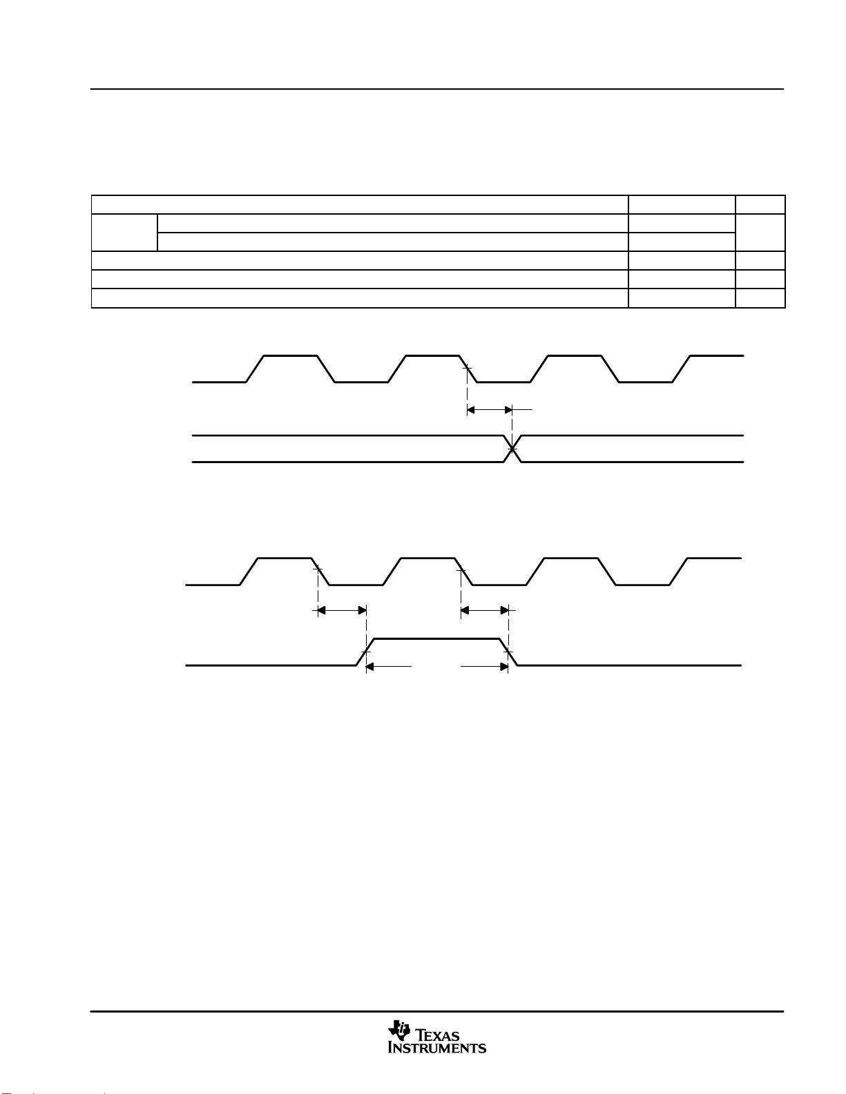
5.13 External Flag (XF) and TOUT Timings
Electrical Specifications
Table 5−20 assumes testing over recommended operating conditions and H = 0.5t
Figure 5−20).
Table 5−20. External Flag (XF) and TOUT Switching Characteristics
PARAMETER MIN MAX UNIT
t
d(XF)
t
d(TOUTH)
t
d(TOUTL)
t
w(TOUT)
Delay time, CLKOUT low to XF high − 1 4
Delay time, CLKOUT low to XF low − 1 4
Delay time, CLKOUT low to TOUT high − 1 4 ns
Delay time, CLKOUT low to TOUT low − 1 4 ns
Pulse duration, TOUT 2H − 4 ns
CLKOUT
XF
Figure 5−19. External Flag (XF) Timing
t
d(XF)
(see Figure 5−19 and
c(CO)
ns
CLKOUT
TOUT
t
d(TOUTH)
t
w(TOUT)
Figure 5−20. TOUT Timing
t
d(TOUTL)
November 2001 − Revised April 2004 SPRS007D
91
Page 92

Electrical Specifications
5.14 Multichannel Buffered Serial Port (McBSP) Timing
5.14.1 McBSP Transmit and Receive Timings
Table 5−21 and Table 5−22 assume testing over recommended operating conditions (see Figure 5−21 and
Figure 5−22).
Table 5−21. McBSP T
ransmit and Receive Timing Requirements
†
MIN MAX UNIT
t
c(BCKRX)
t
w(BCKRX)
t
su(BFRH-BCKRL)
t
h(BCKRL-BFRH)
t
su(BDRV-BCKRL)
t
h(BCKRL-BDRV)
t
su(BFXH-BCKXL)
t
h(BCKXL-BFXH)
t
r(BCKRX)
t
f(BCKRX)
†
CLKRP = CLKXP = FSRP = FSXP = 0. If the polarity of any of the signals is inverted, then the timing references of that signal are also inverted.
‡
P = 0.5 * processor clock
Cycle time, BCLKR/X BCLKR/X ext 4P
Pulse duration, BCLKR/X high or BCLKR/X low BCLKR/X ext 2P−1
Setup time, external BFSR high before BCLKR low
Hold time, external BFSR high after BCLKR low
Setup time, BDR valid before BCLKR low
Hold time, BDR valid after BCLKR low
Setup time, external BFSX high before BCLKX low
Hold time, external BFSX high after BCLKX low
BCLKR int 8
BCLKR ext
BCLKR int 1
BCLKR ext
BCLKR int 7
BCLKR ext
BCLKR int 2
BCLKR ext
BCLKX int 10
BCLKX ext
BCLKX int 0
BCLKX ext
Rise time, BCKR/X BCLKR/X ext 6 ns
Fall time, BCKR/X BCLKR/X ext 6 ns
‡
‡
1
2
1
3
1
2
ns
ns
ns
ns
ns
ns
ns
ns
92
November 2001 − Revised April 2004SPRS007D
Page 93

Electrical Specifications
Disable time, BCLKX high to BDX high impedance following last data
Delay time, BFSX high to BDX valid
Table 5−22. McBSP Transmit and Receive Switching Characteristics
PARAMETER
t
c(BCKRX)
t
w(BCKRXH)
t
w(BCKRXL)
t
d(BCKRH-BFRV)
t
d(BCKXH-BFXV)
t
dis(BCKXH-BDXHZ)
t
d(BCKXH-BDXV)
t
d(BFXH-BDXV)
†
CLKRP = CLKXP = FSRP = FSXP = 0. If the polarity of any of the signals is inverted, then the timing references of that signal are also inverted.
‡
P = 0.5 * processor clock
§
T = BCLKRX period = (1 + CLKGDV) * 2P
Cycle time, BCLKR/X BCLKR/X int 4P
Pulse duration, BCLKR/X high BCLKR/X int D − 1§D + 1
Pulse duration, BCLKR/X low BCLKR/X int C − 1§C + 1
Delay time, BCLKR high to internal BFSR valid
Delay time, BCLKX high to internal BFSX valid
Disable time, BCLKX high to BDX high impedance following last data
bit of transfer
Delay time, BCLKX high to BDX valid
DXENA = 0
Delay time, BFSX high to BDX valid
ONLY applies when in data delay 0 (XDATDLY = 00b) mode
BCLKR int − 3 3 ns
BCLKR ext
BCLKX int − 1 5
BCLKX ext
BCLKX int 6
BCLKX ext
BCLKX int − 1
#
BCLKX ext 2 20
BFSX int −1
BFSX ext 2 11
†
MIN MAX UNIT
‡
ns
§
ns
§
ns
0 12 ns
10
10
ns
ns
ns
7
ns
2 10
¶
¶
C = BCLKRX low pulse width = T/2 when CLKGDV is odd or zero and = (CLKGDV/2) * 2P when CLKGDV is even
D = BCLKRX high pulse width = T/2 when CLKGDV is odd or zero and = (CLKGDV/2 + 1) * 2P when CLKGDV is even
¶
Minimum delay times also represent minimum output hold times.
#
The transmit delay enable (DXENA) feature of the McBSP is not implemented on the TMS320VC5407/TMS320VC5404.
BCLKR
BFSR (int)
BFSR (ext)
BDR
t
d(BCKRH-BFRV)
t
su(BFRH-BCKRL)
t
c(BCKRX)
t
t
su(BDRV-BCKRL)
w(BCKRXH)
t
w(BCKRXL)
t
d(BCKRH-BFRV)
t
h(BCKRL-BFRH)
Bit(n-1)
t
t
h(BCKRL-BDRV)
Figure 5−21. McBSP Receive Timings
r(BCKRX)
(n-2) (n-3)
t
f(BCKRX)
November 2001 − Revised April 2004 SPRS007D
93
Page 94

Electrical Specifications
BCLKX
t
d(BCKXH-BFXV)
BFSX (int)
t
su(BFXH-BCKXL)
BFSX (ext)
BFSX
(XDATDLY=00b)
t
dis(BCKXH-BDXHZ)
BDX
t
c(BCKRX)
t
d(BFXH-BDXV)
t
w(BCKRXH)
t
w(BCKRXL)
t
h(BCKXL-BFXH)
t
d(BCKXH-BDXV)
t
r(BCKRX)
t
d(BCKXH-BDXV)
Bit 0 Bit(n-1) (n-2) (n-3)
Figure 5−22. McBSP Transmit Timings
t
f(BCKRX)
94
November 2001 − Revised April 2004SPRS007D
Page 95

5.14.2 McBSP General-Purpose I/O Timing
Table 5−23 and Table 5−24 assume testing over recommended operating conditions (see Figure 5−23).
Table 5−23. McBSP General-Purpose I/O Timing Requirements
t
su(BGPIO-COH)
t
h(COH-BGPIO)
†
BGPIOx refers to BCLKRx, BFSRx, BDRx, BCLKXx, or BFSXx when configured as a general-purpose input.
Setup time, BGPIOx input mode before CLKOUT high
Hold time, BGPIOx input mode after CLKOUT high
Table 5−24. McBSP General-Purpose I/O Switching Characteristics
PARAMETER MIN MAX UNIT
t
d(COH-BGPIO)
‡
BGPIOx refers to BCLKRx, BFSRx, BCLKXx, BFSXx, or BDXx when configured as a general-purpose output.
Delay time, CLKOUT high to BGPIOx output mode
†
†
‡
Electrical Specifications
MIN MAX UNIT
7 ns
0 ns
− 2 4 ns
t
su(BGPIO-COH)
t
d(COH-BGPIO)
CLKOUT
t
h(COH-BGPIO)
BGPIOx Input
BGPIOx Output
†
BGPIOx refers to BCLKRx, BFSRx, BDRx, BCLKXx, or BFSXx when configured as a general-purpose input.
‡
BGPIOx refers to BCLKRx, BFSRx, BCLKXx, BFSXx, or BDXx when configured as a general-purpose output.
Mode
Mode
†
‡
Figure 5−23. McBSP General-Purpose I/O Timings
November 2001 − Revised April 2004 SPRS007D
95
Page 96

Electrical Specifications
5.14.3 McBSP as SPI Master or Slave Timing
Table 5−25 to Table 5−32 assume testing over recommended operating conditions (see Figure 5−24,
Figure 5−25, Figure 5−26, and Figure 5−27).
Table 5−25. McBSP as SPI Master or Slave Timing Requirements (CLKSTP = 10b, CLKXP = 0)
MASTER SLAVE
MIN MAX MIN MAX
t
su(BDRV-BCKXL)
t
h(BCKXL-BDRV)
†
For all SPI slave modes, CLKG is programmed as 1/2 of the CPU clock by setting CLKSM = CLKGDV = 1.
‡
P = 0.5 * processor clock
Setup time, BDR valid before BCLKX low 12 2 − 6P
Hold time, BDR valid after BCLKX low 4 5 + 12P
‡
‡
Table 5−26. McBSP as SPI Master or Slave Switching Characteristics (CLKSTP = 10b, CLKXP = 0)
PARAMETER
t
h(BCKXL-BFXL)
t
d(BFXL-BCKXH)
t
d(BCKXH-BDXV)
t
dis(BCKXL-BDXHZ)
t
dis(BFXH-BDXHZ)
t
d(BFXL-BDXV)
†
For all SPI slave modes, CLKG is programmed as 1/2 of the CPU clock by setting CLKSM = CLKGDV = 1.
‡
P = 0.5 * processor clock
§
T = BCLKX period = (1 + CLKGDV) * 2P
C = BCLKX low pulse width = T/2 when CLKGDV is odd or zero and = (CLKGDV/2) * 2P when CLKGDV is even
¶
FSRP = FSXP = 1. As a SPI master, BFSX is inverted to provide active-low slave-enable output. As a slave, the active-low signal input on BFSX
Hold time, BFSX low after BCLKX low
Delay time, BFSX low to BCLKX high
Delay time, BCLKX high to BDX valid − 4 5 6P + 2‡10P + 17
Disable time, BDX high impedance following last data bit from
BCLKX low
Disable time, BDX high impedance following last data bit from
BFSX high
Delay time, BFSX low to BDX valid 4P+ 2‡8P + 17
¶
#
MASTER
MIN MAX MIN MAX
T − 3 T + 4 ns
C − 4 C + 3 ns
C − 2 C + 3 ns
§
2P− 4‡6P + 17
SLAVE
†
UNIT
ns
ns
†
UNIT
‡
ns
‡
ns
‡
ns
and BFSR is inverted before being used internally.
CLKXM = FSXM = 1, CLKRM = FSRM = 0 for master McBSP
CLKXM = CLKRM = FSXM = FSRM = 0 for slave McBSP
#
BFSX should be low before the rising edge of clock to enable slave devices and then begin a SPI transfer at the rising edge of the master clock
(BCLKX).
96
BCLKX
BFSX
BDX
BDR
LSB
t
h(BCKXL-BFXL)
t
dis(BFXH-BDXHZ)
t
dis(BCKXL-BDXHZ)
Bit 0 Bit(n-1) (n-2) (n-3) (n-4)
t
su(BDRV-BCLXL)
Bit 0 Bit(n-1) (n-2) (n-3) (n-4)
MSB
t
d(BFXL-BCKXH)
t
d(BFXL-BDXV)
t
d(BCKXH-BDXV)
t
h(BCKXL-BDRV)
Figure 5−24. McBSP Timing as SPI Master or Slave: CLKSTP = 10b, CLKXP = 0
November 2001 − Revised April 2004SPRS007D
Page 97

Electrical Specifications
Table 5−27. McBSP as SPI Master or Slave Timing Requirements (CLKSTP = 11b, CLKXP = 0)
MASTER SLAVE
MIN MAX MIN MAX
t
su(BDRV-BCKXL)
t
h(BCKXH-BDRV)
†
For all SPI slave modes, CLKG is programmed as 1/2 of the CPU clock by setting CLKSM = CLKGDV = 1.
‡
P = 0.5 * processor clock
Setup time, BDR valid before BCLKX low 12 2 − 6P
Hold time, BDR valid after BCLKX high 4 5 + 12P
‡
‡
Table 5−28. McBSP as SPI Master or Slave Switching Characteristics (CLKSTP = 11b, CLKXP = 0)
PARAMETER
t
h(BCKXL-BFXL)
t
d(BFXL-BCKXH)
t
d(BCKXL-BDXV)
t
dis(BCKXL-BDXHZ)
t
d(BFXL-BDXV)
†
For all SPI slave modes, CLKG is programmed as 1/2 of the CPU clock by setting CLKSM = CLKGDV = 1.
‡
P = 0.5 * processor clock
§
T = BCLKX period = (1 + CLKGDV) * 2P
Hold time, BFSX low after BCLKX low
Delay time, BFSX low to BCLKX high
Delay time, BCLKX low to BDX valid − 4 5 6P + 2‡10P + 17
Disable time, BDX high impedance following last data bit from
BCLKX low
Delay time, BFSX low to BDX valid D − 2 D + 4 4P + 2‡8P + 17
¶
#
MASTER
MIN MAX MIN MAX
C −3 C + 4 ns
T − 4 T + 3 ns
§
SLAVE
− 2 4 6P − 4‡10P + 17
†
UNIT
ns
ns
†
UNIT
‡
ns
‡
ns
‡
ns
C = BCLKX low pulse width = T/2 when CLKGDV is odd or zero and = (CLKGDV/2) * 2P when CLKGDV is even
D = BCLKX high pulse width = T/2 when CLKGDV is odd or zero and = (CLKGDV/2 + 1) * 2P when CLKGDV is even
¶
FSRP = FSXP = 1. As a SPI master, BFSX is inverted to provide active-low slave-enable output. As a slave, the active-low signal input on BFSX
and BFSR is inverted before being used internally.
CLKXM = FSXM = 1, CLKRM = FSRM = 0 for master McBSP
CLKXM = CLKRM = FSXM = FSRM = 0 for slave McBSP
#
BFSX should be low before the rising edge of clock to enable slave devices and then begin a SPI transfer at the rising edge of the master clock
(BCLKX).
BCLKX
BFSX
t
dis(BCKXL-BDXHZ)
BDX
BDR
LSB
t
h(BCKXL-BFXL)
t
d(BFXL-BDXV)
Bit 0 Bit(n-1) (n-2) (n-3) (n-4)
t
su(BDRV-BCKXL)
Bit 0 Bit(n-1) (n-2) (n-3) (n-4)
MSB
t
d(BFXL-BCKXH)
t
d(BCKXL-BDXV)
t
h(BCKXH-BDRV)
Figure 5−25. McBSP Timing as SPI Master or Slave: CLKSTP = 11b, CLKXP = 0
November 2001 − Revised April 2004 SPRS007D
97
Page 98

Electrical Specifications
Table 5−29. McBSP as SPI Master or Slave Timing Requirements (CLKSTP = 10b, CLKXP = 1)
MASTER SLAVE
MIN MAX MIN MAX
t
su(BDRV-BCKXH)
t
h(BCKXH-BDRV)
†
For all SPI slave modes, CLKG is programmed as 1/2 of the CPU clock by setting CLKSM = CLKGDV = 1.
‡
P = 0.5 * processor clock
Setup time, BDR valid before BCLKX high 12 2 − 6P
Hold time, BDR valid after BCLKX high 4 5 + 12P
‡
‡
Table 5−30. McBSP as SPI Master or Slave Switching Characteristics (CLKSTP = 10b, CLKXP = 1)
PARAMETER
t
h(BCKXH-BFXL)
t
d(BFXL-BCKXL)
t
d(BCKXL-BDXV)
t
dis(BCKXH-BDXHZ)
t
dis(BFXH-BDXHZ)
t
d(BFXL-BDXV)
†
For all SPI slave modes, CLKG is programmed as 1/2 of the CPU clock by setting CLKSM = CLKGDV = 1.
‡
P = 0.5 * processor clock
§
T = BCLKX period = (1 + CLKGDV) * 2P
D = BCLKX high pulse width = T/2 when CLKGDV is odd or zero and = (CLKGDV/2 + 1) * 2P when CLKGDV is even
¶
FSRP = FSXP = 1. As a SPI master, BFSX is inverted to provide active-low slave-enable output. As a slave, the active-low signal input on BFSX
Hold time, BFSX low after BCLKX high
Delay time, BFSX low to BCLKX low
Delay time, BCLKX low to BDX valid − 4 5 6P + 2‡10P + 17
Disable time, BDX high impedance following last data bit from
BCLKX high
Disable time, BDX high impedance following last data bit from
BFSX high
Delay time, BFSX low to BDX valid 4P + 2‡8P + 17
¶
#
MASTER
MIN MAX MIN MAX
T − 3 T + 4 ns
D − 4 D + 3 ns
D − 2 D + 3 ns
§
2P − 4‡6P + 17
SLAVE
†
UNIT
ns
ns
†
UNIT
‡
ns
‡
ns
‡
ns
and BFSR is inverted before being used internally.
CLKXM = FSXM = 1, CLKRM = FSRM = 0 for master McBSP
CLKXM = CLKRM = FSXM = FSRM = 0 for slave McBSP
#
BFSX should be low before the rising edge of clock to enable slave devices and then begin a SPI transfer at the rising edge of the master clock
(BCLKX).
98
BCLKX
BFSX
BDX
BDR
LSB
t
h(BCKXH-BFXL)
t
dis(BFXH-BDXHZ)
t
dis(BCKXH-BDXHZ)
Bit 0 Bit(n-1) (n-2) (n-3) (n-4)
t
su(BDRV-BCKXH)
Bit 0 Bit(n-1) (n-2) (n-3) (n-4)
MSB
t
d(BFXL-BCKXL)
t
d(BFXL-BDXV)
t
d(BCKXL-BDXV)
t
h(BCKXH-BDRV)
Figure 5−26. McBSP Timing as SPI Master or Slave: CLKSTP = 10b, CLKXP = 1
November 2001 − Revised April 2004SPRS007D
Page 99

Electrical Specifications
Table 5−31. McBSP as SPI Master or Slave Timing Requirements (CLKSTP = 11b, CLKXP = 1)
MASTER SLAVE
MIN MAX MIN MAX
t
su(BDRV-BCKXL)
t
h(BCKXL-BDRV)
†
For all SPI slave modes, CLKG is programmed as 1/2 of the CPU clock by setting CLKSM = CLKGDV = 1.
‡
P = 0.5 * processor clock
Setup time, BDR valid before BCLKX low 12 2 − 6P
Hold time, BDR valid after BCLKX low 4 5 + 12P
‡
‡
Table 5−32. McBSP as SPI Master or Slave Switching Characteristics (CLKSTP = 11b, CLKXP = 1)
PARAMETER
t
h(BCKXH-BFXL)
t
d(BFXL-BCKXL)
t
d(BCKXH-BDXV)
t
dis(BCKXH-BDXHZ)
t
d(BFXL-BDXV)
†
For all SPI slave modes, CLKG is programmed as 1/2 of the CPU clock by setting CLKSM = CLKGDV = 1.
‡
P = 0.5 * processor clock
§
T = BCLKX period = (1 + CLKGDV) * 2P
Hold time, BFSX low after BCLKX high
Delay time, BFSX low to BCLKX low
Delay time, BCLKX high to BDX valid − 4 5 6P + 2‡10P + 17
Disable time, BDX high impedance following last data bit from
BCLKX high
Delay time, BFSX low to BDX valid C − 2 C + 4 4P + 2‡8P + 17
¶
#
MASTER
MIN MAX MIN MAX
D − 3 D + 4 ns
T − 4 T + 3 ns
§
SLAVE
− 2 4 6P − 4‡10P + 17
†
UNIT
ns
ns
†
UNIT
‡
ns
‡
ns
‡
ns
C = BCLKX low pulse width = T/2 when CLKGDV is odd or zero and = (CLKGDV/2) * 2P when CLKGDV is even
D = BCLKX high pulse width = T/2 when CLKGDV is odd or zero and = (CLKGDV/2 + 1) * 2P when CLKGDV is even
¶
FSRP = FSXP = 1. As a SPI master, BFSX is inverted to provide active-low slave-enable output. As a slave, the active-low signal input on BFSX
and BFSR is inverted before being used internally.
CLKXM = FSXM = 1, CLKRM = FSRM = 0 for master McBSP
CLKXM = CLKRM = FSXM = FSRM = 0 for slave McBSP
#
BFSX should be low before the rising edge of clock to enable slave devices and then begin a SPI transfer at the rising edge of the master clock
(BCLKX).
BCLKX
BFSX
t
dis(BCKXH-BDXHZ)
BDX
BDR
LSB
t
h(BCKXH-BFXL)
t
d(BFXL-BDXV)
Bit 0 Bit(n-1) (n-2) (n-3) (n-4)
t
su(BDRV-BCKXL)
Bit 0 Bit(n-1) (n-2) (n-3) (n-4)
MSB
t
d(BFXL-BCKXL)
t
d(BCKXH-BDXV)
t
h(BCKXL-BDRV)
Figure 5−27. McBSP Timing as SPI Master or Slave: CLKSTP = 11b, CLKXP = 1
November 2001 − Revised April 2004 SPRS007D
99
Page 100
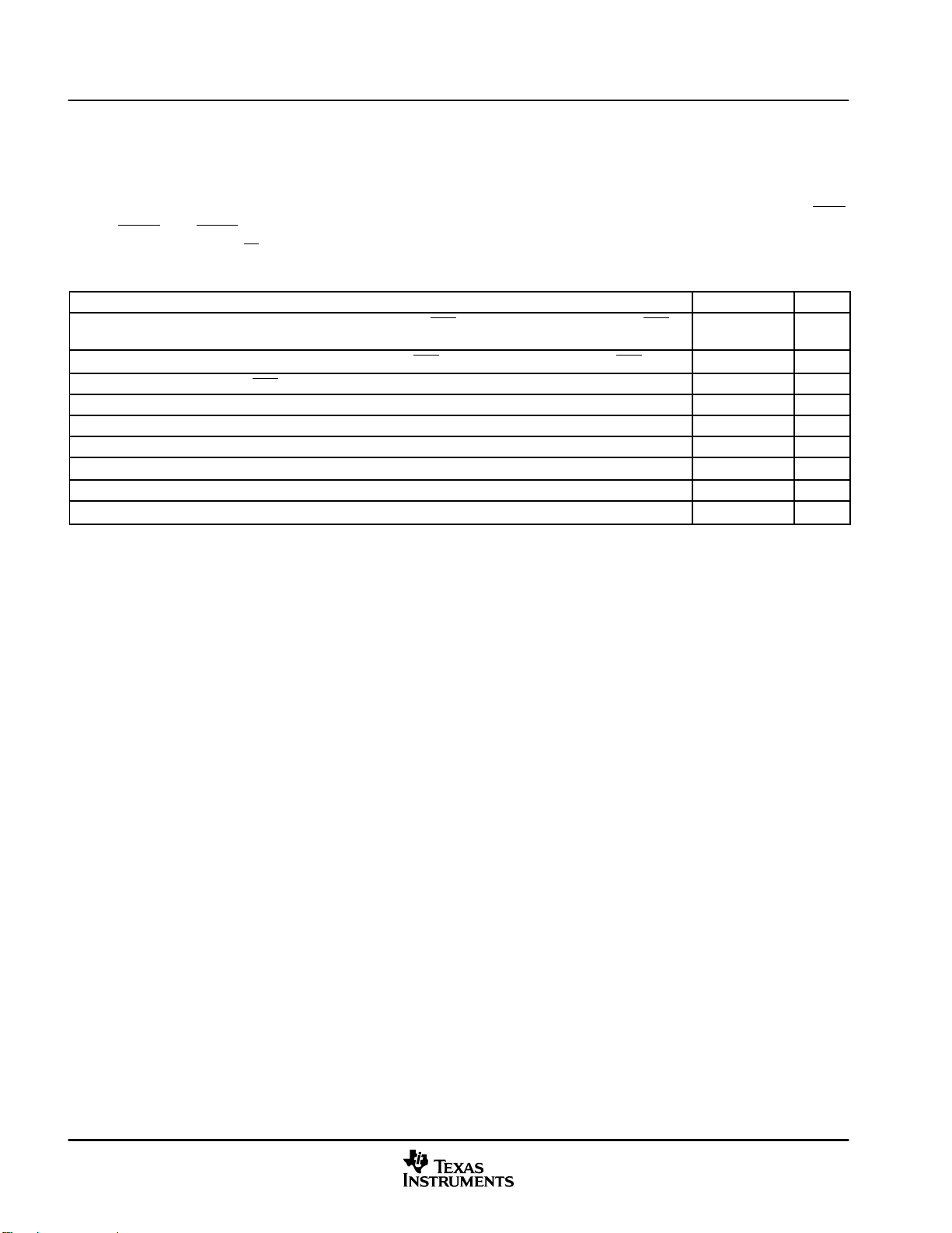
Electrical Specifications
5.15 Host-Port Interface Timing
5.15.1 HPI8 Mode
Table 5−33 and Table 5−34 assume testing over recommended operating conditions and P = 0.5 * processor
clock (see Figure 5−28 through Figure 5−31). In the following tables, DS refers to the logical OR of HCS
HDS1
, and HDS2. HD refers to any of the HPI data bus pins (HD0, HD1, HD2, etc.). HAD stands for HCNTL0,
HCNTL1, and HR/W
t
su(HBV-DSL)
t
h(DSL-HBV)
t
su(HSL-DSL)
t
w(DSL)
t
w(DSH)
t
su(HDV-DSH)
t
h(DSH-HDV)W
t
su(GPIO-COH)
t
h(GPIO-COH)
Setup time, HBIL valid before DS low (when HAS is not used), or HBIL valid before HAS
low
Hold time, HBIL valid after DS low (when HAS is not used), or HBIL valid after HAS low 3 ns
Setup time, HAS low before DS low 8 ns
Pulse duration, DS low 13 ns
Pulse duration, DS high 7 ns
Setup time, HD valid before DS high, HPI write 3 ns
Hold time, HD valid after DS high, HPI write 2 ns
Setup time, HDx input valid before CLKOUT high, HDx configured as general-purpose input 3 ns
Hold time, HDx input valid before CLKOUT high, HDx configured as general-purpose input 0 ns
.
Table 5−33. HPI8 Mode Timing Requirements
,
MIN MAX UNIT
6 ns
100
November 2001 − Revised April 2004SPRS007D
 Loading...