

Page 1

Application Report
SPRAAC7B – April 2006
TMS320TCI6482 Design Guide and Migration from
TMS320TCI100
Rick Hennessy and Douglas Harrington.................................................. Digital Signal Processing Solutions
ABSTRACT
This document describes system design considerations for the TMS320TCI6482
(TCI6482). It also gives comparisons to designing with the TMS320TCI100 (TCI100) for
those familiar with that device. The objective of this document is to cover system
design considerations for the TCI6482. Those familiar with the TCI100 can use the
comparisons to migrate a TCI100 design to the TCI6482. In some cases there is
information overlapping with the TCI6482 data manual. If the information does not
match the data manual information takes precedence.
Contents
1 TCI6482 Documentation ........................................................................... 3
2 Device Overview with Comparison to the TCI100 .............................................. 3
3 Device Identification (ID) ........................................................................... 5
4 Pin and Package Compatibility ................................................................... 5
5 Device Configurations and Initialization ......................................................... 6
6 Clocking .............................................................................................. 8
7 Power Supply ..................................................................................... 14
8 I/O Buffers .......................................................................................... 21
9 Peripheral Section ................................................................................ 22
Appendix A TCI6482 RGMII 1.5V/1.8V to 2.5V/3.3V Translation ............................... 40
List of Figures
1 CLKIN1, CLKIN2 Single Device Clock Solution ............................................... 10
2 PLL1, PLL2 Multiple Device Clock Solution ................................................... 11
3 RIOCLK Single Device LVDS Clock Solution ................................................. 12
4 RIOCLK Multiple Devices LVDS Clock Solution .............................................. 12
5 RIOCLK Multiple Devices LVDS Clock Solution .............................................. 13
6 RIOCLK Multiple Devices LVPECL Clock Solution ........................................... 13
7 Power Supply Generation ........................................................................ 15
8 Recommended Power Supply Filter ............................................................ 16
9 Reference Voltage Generation .................................................................. 16
10 Multiple DSP Remote Sense Connections .................................................... 18
11 Single DSP Remote Sense Connections ...................................................... 19
12 McBSP 8 Load Routing Topology .............................................................. 27
13 HSTL to LVCMOS Translation .................................................................. 35
14 VLYNQ Clock Divider Example ................................................................. 37
A-1 RGMII Voltage Level Translation Circuit ....................................................... 40
A-2 VOUT vs VIN ...................................................................................... 42
A-3 125MHz Signal from A2 to B2 and From B3 to A3 ........................................... 43
List of Tables
1 TCI6482 Features, Comparison to TCI100 Processor......................................... 4
SPRAAC7B – April 2006 TMS320TCI6482 Design Guide and Migration from TMS320TCI100 1
Submit Documentation Feedback
Page 2

www.ti.com
2 TCI6482 and TCI100 JTAG (BSDL) IDs ......................................................... 5
3 Pin and Package Differences ..................................................................... 6
4 Clocking Differences between TCI6482 and TCI100 .......................................... 8
5 Reference Clock Requirements .................................................................. 9
6 Power Supply Differences ....................................................................... 14
7 Die Voltage Monitor Pins ......................................................................... 18
8 Bulk Capacitor Examples ........................................................................ 20
9 Capacitor Recommendations .................................................................... 20
10 PTV Compensated Interfaces ................................................................... 22
11 EMIFA Comparsion: TCI6482 vs TCI100 ...................................................... 24
12 HPI Comparison: TCI6482 vs TCI100 .......................................................... 25
13 PCI Comparison: TCI6482 vs TCI100 .......................................................... 26
14 McBSP Comparison: TCI6482 vs TCI100 ..................................................... 27
15 VCP2 Summary of Changes on TCI6482 ...................................................... 28
16 VCP2 Usage Change on TCI6482 .............................................................. 28
17 VCP2 Register Changes on TCI6482 .......................................................... 29
18 TCP2 Summary of Changes on TCI6482 ...................................................... 29
19 TCP2 Usage Change on TCI6482 .............................................................. 30
20 TCP2 Register Changes on TCI6482 .......................................................... 30
21 GPIO/Interrupt Comparison: TCI6482 vs TCI100 ............................................. 31
22 Timer Comparison: TCI6482 vs TCI100 ....................................................... 32
23 SRIO PLL Multiplier Settings .................................................................... 37
24 JTAG/Emulation Comparison: TCI6482 vs TCI100........................................... 39
2 TMS320TCI6482 Design Guide and Migration from TMS320TCI100 SPRAAC7B – April 2006
Submit Documentation Feedback
Page 3

www.ti.com
TCI6482 Documentation
1 TCI6482 Documentation
The following is a list of available documents relevant to a TCI6482 based design:
• Data Manual
– TMS320TCI6482 Communications Infrastructure Digital Signal Processor, (SPRS246 ). Referred to
in this document as the TCI6482 data manual.
• User Guides / Reference Manuals
– TMS320C64x/C64x+ DSP CPU and Instruction Set Reference Guide (SPRU732 )
– TMS320C64x+ Megamodule Reference Guide (SPRU871 )
– TMS320C64x+ DSP Cache User's Guide (SPRU862 )
– TMS320C6000 Programmer's Guide (SPRU198 )
– TMS320TCI648x DSP PLL Controller Reference Guide (SPRU806)
– TCI648x DSP External Memory Interface (EMIF) Reference Guide (SPRU925)
– TMS320TCI6482 Bootloader User's Guide
– TMS320TCI6482 Preliminary Power Consumption Summary
– TCI648x DSP UHPI User’s Guide (SPRU874)
– TCI648x DSP PCI Reference Guide (SPRUE60)
– TMS320C6000 DSP Multichannel Buffered Serial Port (McBSP) Reference Guide (SPRU803 )
– TMS320TCI648x DSP Viterbi-Decoder Coprocessor (VCP) Reference Guide (SPRUE09)
– TMS320TCI648x DSP Turbo-Decoder Coprocessor (TCP) Reference Guide (SPRUE10)
– TCI648x DSP General-Purpose Input/Output (GPIO) User’s Guide (SPRU725)
– TMS320TCI648x DSP 64-Bit Timer User's Guide (SPRU818)
– TMS320TCI648x DSP Enhanced DMA (EDMA) Controller User’s Guide (SPRU727)
– TCI6482 DSP Inter-Integrated Circuit (I²C) Module User's Guide (SPRUE11)
– TMS320TCI648x DSP Ethernet Media Access Controller (EMAC)/Management Data Input/Output
(MDIO) User’s Guide (SPRUE12)
– TMS320TCI648x DSP Universal Test and Operations PHY Interface for ATM 2 (Utopia2) User’s
Guide(SPRU726)
– Serial RapidIO User’s Guide (SPRUE13 )
– TMS320TCI648x DSP DDR2 Memory Controller User's Guide (SPRU894)
– High Speed DSP Systems Design Reference Guide (SPRU889 )
– 60-Pin Emulation Header Technical Reference (SPRU655A )
• Application Notes
– EDMA v3.0 (EDMA3) Migration Guide for TMS320TCI648x DSP (SPRAAC1 )
– Implementing Serial Rapid I/O PCB Layout on a TMS320TCI6482 Hardware Design (SPRAAB0 )
– Implementing DDR2 PCB Layout on the TMS320TCI6482 (SPRAAA9 )
– Using IBIS Models for Timing Analysis (SPRA839 )
• Misc
– TCI6482 IBIS Model File
– TMS320TCI6482 BSDL file
2 Device Overview with Comparison to the TCI100
A high level comparison of the TCI6482 and TCI100/TCI100Q features is given in Table 1 . This table does
not cover software differences. For more detailed comparisons of peripherals refer to the peripheral
sections later in this document.
SPRAAC7B – April 2006 TMS320TCI6482 Design Guide and Migration from TMS320TCI100 3
Submit Documentation Feedback
Page 4

www.ti.com
Device Overview with Comparison to the TCI100
Table 1. TCI6482 Features, Comparison to TCI100 Processor
Hardware Features TCI6482 TCI100/TCI100Q
Peripherals EMIFA (64-bit data 1 EMIFA (64-bit data 1
Not all peripheral pins bus) bus)
are available at the (Clock source = (Clock source =
same time. (For more AECLKIN or AECLKIN, CPU/4,
details, see the SYSCLK4) CPU/6)
Device Configuration (Supports SBSRAM, (Supports SBSRAM,
section of the device SRAM, Sync FIFOs, SRAM, Sync FIFOs,
data manual) Async memories; Async memories;
SRAM, ROM, Flash) SRAM, ROM, Flash)
generated from PLL2)
[CPU/3 clock rate]
High-speed 1x/4x 1 N/A N/A
Serial Rapid IO Port
HPI (32 or 16-bit user 1 same 1
[66-MHz or 33-MHz] [33-MHz]
(Internal clock source
UTOPIA (8-bit mode, 1 Same
50-MHz, Slave-only)
10/100/1000 Ethernet 1 N/A N/A
Management Data 1 N/A N/A
Input/Output (MDIO)
(Internal clock source:
External clock source
up to CPU clock/24)
General Purpose 16 General Purpose 16
Input/Output (all can Input/Output (4 can
be used as external be used as external
Decoders VCP2 1 VCP 1
Coprocessors
On-Chip Memory L1P 32K-Byte L1P 16K-Byte
cache and SRAM)
cache and SRAM)
CPU MegaModule Revision ID Register Read value: 0x0 N/A N/A
Revision ID (MM_REVID[15:0]) (silicon revision 1.1)
DDR Memory 1 EMIFB (16-bit bus N/A
Controller EMIF width)
(32-bit data bus (supports SDRAM
width) [1.8V IO] and programmable
(Clock source = sync)
EDMA3 (64 1 EDMA2 1
independent
channels)
selectable)
PCI (32-bit) 1 PCI (32-bit) 1
McBSP 2 McBSP 3
up to 90 MHz)
MAC (EMAC)
64-bit Timers 2 - 64-bit or 32-bit Timer 3-32 bit timers
(Configurable) 4-32-bit
CPU Clock/6,
VLYNQ 1 N/A N/A
interrupts) interrupts)
TCP2 1 TCP 1
RSA 1 N/A N/A
(Configurable as (Cache only)
L1D 32K-Byte L1D 16K-Byte
(Configurable as (Cache only)
L2 2048K-Byte L2 1024K-Byte
Byte address =
0x01812000
4 TMS320TCI6482 Design Guide and Migration from TMS320TCI100 SPRAAC7B – April 2006
Submit Documentation Feedback
Page 5

www.ti.com
Table 1. TCI6482 Features, Comparison to TCI100 Processor (continued)
JTAG BSDL_ID JTAGID register Read value: 0x0008A02F JTAGID register Read value: 0x008102F
Frequency Core clock Up to 1-GHz Core clock 720MHz,
Voltage Core Supply 1.2V Core Supply 1.2V
PLL and PLL PLL1 for Core Clock PLL for Core Clock
controller Options (Software (Hardware
BGA Package 697-Pin BGA ZTZ Suffix 532-Pin BGA GLZ Suffix
Process Technology 0.09um/7-Level Cu 0.09um/7-Level Cu
Device Part Numbers TMX320TCI6482ZTZ TMS320TCI100GLZ
3 Device Identification (ID)
The JTAG (BSDL) ID and Silicon Revision ID are different than other TMS320C64x DSP devices. The
TCI6482 device IDs are shown in the table below and are referred to as JTAG (BSDL) IDs. The JTAG
(BSDL) ID is accessible via JTAG on both devices and through the JTAG ID register at address
0x02A80008 on the TCI6482 device.
Table 2 identifies the JTAG (BSDL) ID differences between the TCI100 and TCI6482.
Device Identification (ID)
850MHz
IO Supplies 3.3V, 1.8V (1.5), 1.2V IO Supply 3.3V
configurable) configurable)
PLL2 for DDR/EMAC
Clock
Package, 0.8mm Package, 0.8mm
pitch, 24mmx24mm pitch, 23x23mm
Metal Process Metal Process
(CMOS) (CMOS)
(1)
(2)
The TCI6482 does not have a Silicon Revision ID as found in the TCI100.
4 Pin and Package Compatibility
The physical dimensions and pin out of package used for TCI6482 will be different from TCI100.
Modification will be needed to account for the different physical dimensions of package and pin out.
Changes in substrate may also affect the thermal characteristics of the package used for TCI6482. See
the TMS320TCI6482 Communications Infrastructure Digital Signal Processor (SPRS246) for additional
information regarding package characteristics.
Table 2. TCI6482 and TCI100 JTAG (BSDL) IDs
JTAG (BSDL) ID
Device Variant [31:28] Part Number [27:12] Manufacturer [11:1] LSB
TCI6482 xxxxb
TCI100 xxxxb
Variant field indicates the silicon version. Refer to the data manual and errata for current silicon versions.
Variant field indicates the silicon version. Refer to the data manual and errata for current silicon versions.
(1)
(2)
0000000010001010b 00000010111b 1 [0]
0000000010000001b 00000010111b 1
SPRAAC7B – April 2006 TMS320TCI6482 Design Guide and Migration from TMS320TCI100 5
Submit Documentation Feedback
Page 6

www.ti.com
Device Configurations and Initialization
Device Package Type (s) Pin Count
TCI100 GLZ Ball Grid Array (BGA) 0.8mm pitch, 532
TCI6482 ZTZ Ball Grid Array (BGA) 0.8mm pitch, 697
5 Device Configurations and Initialization
On the TCI6482 device, bootmode and certain device configuration/peripheral selections are determined
at device reset, while peripheral usage (enabled/disabled) is determined by the Peripheral Configuration
registers after the device reset. The peripherals on the TCI6482 device are “disabled” and need to be
“enabled”. This is different than the TCI100 in which case the peripherals selected by the boot strap
options were enabled on power-up. The basic information on configuration options, boot modes options
and use of the Power Configuration registers can be found in the TCI6482 data manual.
5.1 Device Reset
There are several ways to reset the TCI6482 and these are described in the TCI6482 data manual. The
two external resets, POR and RESET, need to be driven to a valid logic level at all times. POR must be
asserted (low) on a power-up while the clocks and power planes become stable. RESET can be used
from the powered up state to issue a warm reset, which performs the same as a POR except that test and
emulation logic are not reset. If a warm reset is not needed, RESET can be pulled up to DVDD33.
In revision 1.1 silicon, when POR is held low the internal pull-up and pull-down resistors are disabled. This
requires the use of external pull-up and pull-down resistors for all pins that have their states latched by
POR. Alternatively, after POR is de-asserted long enough for the internal resistors to pull voltage levels to
valid states (> 100uS) bringing RESET low for at least 24 CLKIN1 cycles and then high again will allow
re-latching the state of the configuration strapping with valid values from the internal pull-ups, pull-downs.
While POR is low, large currents may be seen on the DVDD33 power plane due to floating inputs (i.e. the
EMIF bus). If the user wishes to avoid these currents external pull-ups or pull-downs should be used.
Refer to the TCI6482 Silicon Errata document for complete details. In revision 2.0 silicon and later the
internal pull-up and pull-down resistors will not be disabled under any conditions.
The RESETSTATz signal indicates the internal reset state. The RESETSTATz is asserted (low) on a
power-on reset, warm reset, max reset, or system reset. The only reset that does not cause
RESETSTATz to be asserted is a CPU reset (issued from the PCI peripheral).
Table 3. Pin and Package Differences
23 x 23 mm
24 x 24 mm
5.2 Device Configuration
The TCI6482 device configuration options are multiplexed on the EMIFA address AEA[19:0] and EMIFA
bank address lines ABA[1:0]. There is one dedicated configuration pin, PCI_EN. Refer to the TCI6482
data manual for details on the configuration options. All reset strapping pins have internal pull-ups or
pull-downs in the range of 30K ohms. If the EMIFA bus is not used the internal pull-ups and pull-downs
can be used and an external pull-up/down is only needed if the opposite setting is desired. If the
configuration pins are routed out from the device, the internal pullup/pulldown resistor should not be relied
upon; 1K pull-ups and pull-downs are recommended for all desired settings.
The core clock PLL multiplier is not set by reset configuration strapping as it was on the TCI100. The PLL
multiplier can only be set by CPU register writes. The registers are not accessible through boot
peripherals. The core clock speed when accessing the internal ROM must be not more than 750MHz. PCI
and Serial RapidIO boot modes automatically change the PLL multiplier to 15X, so the CLKIN1 must be
no more than 50MHz. For other boot modes it is suggested to set the multiplier early in the boot process
in order to reduce boot times. For details on setting the CLKIN1 PLL multiplier and divider settings refer to
section 6.1 and the TMS320TCI648x DSP PLL Controller Reference Guide (SPRU806).
TMS320TCI6482 Design Guide and Migration from TMS320TCI1006 SPRAAC7B – April 2006
Submit Documentation Feedback
Page 7

www.ti.com
5.3 Peripheral Configuration
Other than the device reset configuration covered in Section 5.1 , all other configurations are done by
register accesses. The first step to configuring a peripheral is to enable it using Peripheral Configuration
Register 0 and 1. Since all peripherals not needed for the selected boot mode are disabled, a first level
boot loader may be needed to enable interfaces needed during the full boot load. For example, if the
application code to be loaded (.OUT file) loads data into an external memory, a first level boot loader must
be loaded and executed to enable the EMIF interface. If the Boot Mode selection specifies a particular
interface for boot, it is automatically enabled and configured. Note that Peripheral Configuration Register 0
and 1 are only accessible by the CPU, therefore, it is not possible to configure these registers directly
through a host interface like the HPI and PCI. For more details on peripheral configuration refer to the
Device Configuration section of the TCI6482 data manual.
The EMAC interface requires some PLL2 configurations. The specific settings are dependent on the MII
mode. For details on PLL2 configuration refer to the TMS320TCI648x DSP PLL Controller Reference
Guide (SPRU806).
For some peripherals, the peripheral operating frequency is dependent on the CPU core clock frequency.
This should be accounted for when configuring the peripheral.
All other peripheral configurations are done within the peripheral module. For configuring the peripheral
module refer to the specific peripheral’s user guide.
5.4 Configuration Tables in I2C ROM
I2C ROM contents can contain Configuration Tables which allow customer defined memory map accesses
during the I2C boot mode. These accesses can be used to configure peripherals during the boot process.
For details refer to the TMS320TCI6482 Bootloader User's Guide document.
Device Configurations and Initialization
5.5 Boot Modes
The interfaces which support a boot loading process are: I2C, HPI, PCI, Serial RapidIO and EMIF (8-bit
ROM). In addition, a first level boot loader (loaded using one of those interfaces) can configure the
Ethernet or Utopia interfaces for a secondary boot load. For a summary of the boot modes supported refer
to the TCI6482 data manual. For details regarding boot modes, refer to the TMS320TCI6482 Bootloader
User's Guide document.
Regardless of the boot mode selected, an emulator connection can always reset the device to acquire
control.
If the PCI interface is enabled, it supports an optional auto-initialization feature which will load the PCI
config registers from an I2C ROM before the boot load is performed.
5.6 Boot/Initialization Sequence
Generic bring up procedure:
1. Follow power-up and reset sequencing per the TCI6482 data manual.
2. When the POR (or RESET on a warm boot) signal is de-asserted the boot strapping options are
latched and the boot mode selection controls what happens next:
a. If the PCI interface is selected and auto-initialization is enabled, the auto-initialization is performed
b. Booting over I2C loads code contents into L2, code is executed after last code section is copied
c. Booting over EMIF starts executing from the base address of CE3 space
d. Booting over HPI, PCI or Serial RapidIO puts the device in a state that waits for code to be copied
through those interfaces into L2 and an interrupt to initiate the execution of that code.
3. Boot code (at a minimum) should configure the PLL1 core clock frequency and also enable and
configure the required peripherals and:
a. PCI and SerialRapidIO boot modes configure the PLL1 for a 15x multiplier to allow proper
operation of those interfaces. After the boot load is completed, application code should change the
PLL1 to final desired multiplier. Due to the use of the 15x multiplier, the CLKIN1 should be no
greater than 50MHz when selecting the PCI or SerialRapidIO boot modes.
SPRAAC7B – April 2006 TMS320TCI6482 Design Guide and Migration from TMS320TCI100 7
Submit Documentation Feedback
Page 8

www.ti.com
Clocking
6 Clocking
6.1 PLLs
6.1.1 Clock PLL and PLL Controller
A description of the PLLs and PLL controllers along with register definitions can be found in the
TMS320TCI6482 Communications Infrastructure Digital Signal Processor (SPRS246). Table 4 shows the
clocking differences between the TCI6482 and the TCI100.
Device PLL Type Input Clock Frequency Program Clock Input Purpose
TCI100 Analog PLL 42MHz - x1, x6, x12, x20 HW config External clock CPU clock
TCI6482 Analog PLL 33 MHz - x15, x20, x25, SW config External clock CPU clock
TCI6482 Analog PLL 12.5MHz - x10 N/A External clock DDR2 and
Table 4. Clocking Differences between TCI6482 and TCI100
Range Multiplication Multiplier via Source
(1)
75MHz
(Main device 66MHz
clock)
(Used for DDR2 26MHz input Ethernet (except
and EMAC MII)
clocking)
(2) (1)
Factors
input
x30, x32 input
(3)
(1)
Supported frequency range and multipliers may change. Refer to the data manual for the latest information.
(2)
Clock range is limited to 50MHz if using PCI or SerialRapidIO boot modes.
(3)
In silicon version 2.0 and all subsequent versions this PLL is not required for RMII operation.
6.1.2 PLL Operation
The PLL1 controller powers up in bypass (x1) mode with PLL1 in reset. Some boot modes change this
multiplier (see Section 5.6 ). After the PLL1 is out of reset and running, changing the PLL1 controller
multiplier and divider values (or the reference clock frequency) involves using the PLL reset mode to clear
the lock condition.
The PLL reset mode is used under the following conditions:
• After power is applied, the PLL is automatically placed in reset mode
• To change the input frequency (CLKIN1)
• To change the value in any divider or multiplier register
The procedures for changing the PLL are described in Section 6.1.3 and Section 6.2 .
6.1.3 PLL Configuration after Power-Up
The following process should be followed to set the PLL multiplier after power-on reset. The wait times are
conservative durations to guarantee proper operation.
1. Allow PLL1 to become stable, see the device data manual for stabilization time.
2. Program PLLCTL.PLLENSRC=0 to enable the PLLCTL.PLLEN bit.
3. Program PREDIV, PLLM for the desired multiplier and divider.
4. Set PLLRST=0 to de-assert PLL reset.
5. Wait for 3000 CLKIN1 cycles for the PLL to lock.
6. Set PLLEN=1 to switch from Bypass mode to PLL mode.
TMS320TCI6482 Design Guide and Migration from TMS320TCI1008 SPRAAC7B – April 2006
Submit Documentation Feedback
Page 9

www.ti.com
6.2 PLL Configuration During Operation
The following process should be followed to change the PLL after it has been operating. The wait times
are conservative durations to guarantee proper operation.
1. Program PLLCTL.PLLENSRC=0 to enable the PLLTL.PLLEN bit.
2. Program PLLEN=0 (PLL bypass mode) and PLLRST=1 (reset PLL) in PLLCTL register.
3. Program PREDIV, PLLM for the desired multiplier and divider.
4. Wait for at least 256 CLKIN1 cycles for the PLL to reset.
5. Set PLLRST=0 to de-assert PLL reset.
6. Wait for 3000 CLKIN1 cycles for the PLL to lock.
7. Set PLLEN=1 to switch from Bypass mode to PLL mode.
6.3 PLL1, PLL2, and SRIO Reference Clock Solutions
This section describes the clock requirements and a system solution for the input clocks to the TCI6482
device that require special consideration. CLKIN1 is the reference clock to PLL1 which is used to generate
the core clock (up to 1GHz). This clock requires a low jitter clock source. CLKIN2 is the reference clock to
PLL2 which is used to generate the clock for the DDR2 and EMAC subsystems. This clock, when used as
the reference clock to the DDR2 subsystem, must be low jitter. The SRIO reference clock (RIOCLK,
RIOCLK) requires a differential low jitter clock source and proper termination.
It is also assumed that multiple TMS320TCI6482 devices may be used on a board so the proposed
system solutions include clock fanout buffers.
Clocking
6.3.1 Clock Requirement
The clock requirements are given in Table 5 .
CLKIN1 LVCMOS or LVTTL 100pS pk-pk Max 1.2nS 40/60% 50PPM 50MHz 1GHz
CLKIN2 LVCMOS or LVTTL 100pS pk-pk Max 1.2nS 40/60% 50PPM 25MHz 250MHz
RIOCLK, Differential LVDS or 4pS RMS 50pS - 45/55% 50PPM 125MHz, 3.125GHz
RIOCLK LVPECL 56ps pk-pk @ 700pS 156.25MHz
(1)
Assumes a Gaussian distribution. Peak-peak jitter assumes 100,000 points.
(2)
Recommended operating frequencies based on component availability and supported PLL multipliers.
Trise/Tfall values are given for CLKIN1 and CLKIN2 transitions from 0.8V to 2.0V. This is equivalent to a
max Trise/Tfall of 2nS from 20% to 80% of 3.3V. RIOCLK Trise/Tfall values are given for 20% to 80% of
the voltage swing. These rise/fall times assume the maximum jitter values. Slower rise/fall times can be
used if the jitter is lower.
6.3.2 CLKIN1/CLKIN2 Solutions
CLKIN1 and CLKIN2 have similar requirements for a clock source so the same clocking solutions (except
for frequency) can be used for both.
6.3.2.1 Single Device Solution
It is assumed that the source clock for each of these clocks is an oscillator on the same board as the
TMS320TCI6482. Use of distributed clocks may require a jitter cleaner device such as the CDCM7005
(refer to http://focus.ti.com/docs/prod/folders/print/cdcm7005.html ). Most PLL based clock generators do
not meet the input jitter requirement. If an on-board oscillator is used with one TMS320TCI6482 no other
components should be needed except for termination resistors.
Logic Input Jitter
Table 5. Reference Clock Requirements
-12
1x10E
BER
(1)
Trise/Tfall Duty Cycle Stability Freq
(2)
PLL Freq
SPRAAC7B – April 2006 TMS320TCI6482 Design Guide and Migration from TMS320TCI100 9
Submit Documentation Feedback
Page 10

www.ti.com
Clocking
For CLKIN1 and CLKIN2, a low jitter CMOS oscillator would be sufficient. A series termination resistor
(nominally 22 ohms) at the source is suggested (refer to Figure 1 ). An example of an appropriate oscillator
is:
• Vectron VCC1 series 3.3V CMOS oscillator
This oscillator has not been tested but is an example of an oscillator that meet the specification
requirements for CLKIN1 and CLKIN2.
6.3.2.2 Fanout Solutions
For systems with multiple TMS320TCI6482 devices it may be preferred to use one oscillator and a fanout
buffer instead of multiple oscillators. This would allow for fewer components as well as lower cost. The
fanout buffer increases the jitter at the clock input so care must be taken in selecting the combination of
oscillator and fanout buffer.
In most cases the same oscillators described in Section 6.3.2.1 can be used for the fan out case. The
oscillator output specifications should be compared to the fanout buffer input specifications to make sure
they are compatible.
A low jitter fanout buffer is required which generally means a non-PLL based fanout buffer should be used.
Suggested solutions for fanout buffers are:
• TI CDCV304 1:4 Clock buffer
• TI CDCVF2310 1:10 Clock buffer
• CDCV304 jitter information: http://focus.ti.com/lit/an/scaa052/scaa052.pdf
• CDCVF2310 jitter information: http://focus.ti.com/lit/an/scaa064/scaa064.pdf
Figure 2 shows a diagram of a solution that allows an oscillator and a fanout buffer to provide CLKIN1 or
CLKIN2 for up to 4 DSPs. Up to 10 DSPs could be supported with the CDCVF2310 which would be the
same circuit without the series resistors since the CDCVF2310 has built-in 22ohm resistors. The buffer
outputs should not be used to drive additional fanout buffers since the jitter will accumulate.
– http://www.vectron.com/products/xo/vcc1.pdf
Figure 1. CLKIN1, CLKIN2 Single Device Clock Solution
– http://focus.ti.com/lit/ds/symlink/cscv304.pdf
– http://focus.ti.com/lit/ds/symlink/cdcvf2310.pdf
10 TMS320TCI6482 Design Guide and Migration from TMS320TCI100 SPRAAC7B – April 2006
Submit Documentation Feedback
Page 11

www.ti.com
Figure 2. PLL1, PLL2 Multiple Device Clock Solution
Clocking
Another solution would be to use very low jitter PLL clock generators/buffers. TI’s CDCE706 and
CDCE906 have been tested with at 25MHz and 50MHz and shown to meet the required jitter
specifications.
6.3.2.3 Layout Recommendations
Placement, Terminations
• The oscillator should be placed close to the destination.
• Series termination should be placed close to clock source.
• The value of the series termination resistor should be optimized to reduce over-shoot and under-shoot
while not violating the Trise/Tfall input specification. TI suggests the customer use IBIS simulations to
determine the correct value of the termination resistor.
Trace Routing
• A GND plane should be placed below the oscillator.
• Digital signals should not be routed near or under the clock sources.
• Maintain at least 25 mil spacing to other traces.
6.3.3 RIOCLK/ RIOCLK Solutions
The SerialRapidIO reference clock requires special considerations because it is differential, must be low
jitter, and requires termination. Either an LVDS or LVPECL clock source can be used but they require
different terminations. The input buffer sets its own common mode voltage so AC coupling is necessary. It
also includes a 100ohm differential termination resistor, eliminating the need for an external 100ohm
termination when using an LVDS driver. For generation information on AC termination schemes, refer to
AC Coupling Between Differential LVPECL, LVDS, HSTL and CML (scaa059 ). For information on DC
coupling refer to DC-Coupling Between Differential LVPECL, LVDS, HSTL, and CML (scaa062 ) .
SPRAAC7B – April 2006 TMS320TCI6482 Design Guide and Migration from TMS320TCI100 11
Submit Documentation Feedback
Page 12

www.ti.com
LOW JITTER
OSCILLATOR
Example:
Pletronics
LV77D
RIOCLK
DSP
RIOCLK
0.01uF
0.01uF
RIOCLK
DSP
LOW JITTER
OSCILLATOR
Example:
Pletronics
PE77D
150 ohm
150 ohm
0.01uF
0.01uF
RIOCLK
Clocking
6.3.3.1 Single Device Solution
It is assumed that the source clock is an oscillator on the same board as the TMS320TCI6482. Use of
distributed clocks may require a jitter cleaner device such as the CDCM7005 (refer to
http://focus.ti.com/docs/prod/folders/print/cdcm7005.html ) or the CDCL6010. If an on-board oscillator is
used with one TMS320TCI6482 no other components should be needed except for terminations.
For the Serial rapid IO reference clock examples of appropriate oscillators are:
• Pletronics LVDS LV77D oscillator
– http://www.pletronics.com/pdf/LV77D%203.3v.pdf
• Pletronics LVPECL PE77D oscillator
– http://www.pletronics.com/pdf/PE77D%203.3v.pdf
These oscillators have not been tested but are examples of oscillators that meet the specification
requirements for RIOCLK/ RIOCLK.
Figure 3 shows an LVDS based solution including terminations. Figure 4 shows an LVPECL based
solution including terminations. The terminations shown are still being investigated and should be
considered preliminary.
Figure 3. RIOCLK Single Device LVDS Clock Solution
Figure 4. RIOCLK Multiple Devices LVDS Clock Solution
6.3.3.2 Fanout Solutions
For systems with multiple TMS320TCI6482 devices it may be preferred to use one oscillator and a fanout
buffer instead of multiple oscillators. This would allow for fewer components as well as lower cost. The
fanout buffer increases the jitter at the clock input so care must be taken in selecting the combination of
oscillator and fanout buffer.
In most cases the same oscillators described in Section 6.3.3.1 can be used for the fan out case. The
oscillator output specifications should be compared to the fanout buffer input specifications to make sure
they are compatible.
12 TMS320TCI6482 Design Guide and Migration from TMS320TCI100 SPRAAC7B – April 2006
A low jitter fanout buffer is required which generally means a non-PLL based fanout buffers should be
used. Suggested solutions for a fanout buffers are:
Submit Documentation Feedback
Page 13

www.ti.com
LOW JITTER
OSCILLATOR
Example:
Pletronics
LV77D
RIOCLK
SN65LVDS108
RIOCLK
DSP1
RIOCLK
DSP8
CLK0
CLK0#
CLKN
CLK7#
100ohms
0.01uF
0.01uF
0.01uF
0.01uF
R I O C LK
R I O C LK
R I O C LK
LOW JITTER
OSCILLATOR
Example:
Pletronics
PE77D
RIOCLK
CDCLVP110
RIOCLK#
RIOCLK
DSP1
RIOCLK#
RIOCLK
DSP10
RIOCLK#
CLK0
CLK0#
CLKN
CLK9#
50 ohm 50 ohm
50 ohm
150
ohm
150
ohm
150
ohm
150
ohm
0.01uF
0.01uF
0.01uF
0.01uF
• TI SN65LVDS108 LVDS 1:8 Clock fanout buffer
– http://focus.ti.com/lit/ds/symlink/sn65lvds108.pdf
• TI CDCLVP110 LVPECL 2:10 Clock fanout buffer
– http://focus.ti.com/lit/ds/symlink/cdclvp110.pdf
There are also 4-port and 16-port versions of the SN65LVDS108. For an integrated jitter cleaner and
multiple clock output buffer the CDCL6010 can be used.
These buffers have not been tested but are examples of buffers that meet the specification requirements
for RIOCLK / RIOCLK.
Jitter performance for the SN65LVDS108 is found in its datasheet. For the CDCLVP110 the jitter
characteristics of these parts refer to:
• CDCLVP110 Jitter Info: http://focus.ti.com/lit/an/scaa068/scaa068.pdf
Figure 5 shows a diagram of a solution that allows an LVDS oscillator and an LVDS fanout buffer to
provide RIOCLK / RIOCLK for up to 8 DSPs. Figure 6 shows an LVPECL solution for up to 10 DSPs. The
fanout buffer outputs should not be used to drive additional fanout buffers since the jitter will accumulate.
Clocking
Figure 5. RIOCLK Multiple Devices LVDS Clock Solution
SPRAAC7B – April 2006 TMS320TCI6482 Design Guide and Migration from TMS320TCI100 13
Submit Documentation Feedback
Figure 6. RIOCLK Multiple Devices LVPECL Clock Solution
Page 14
www.ti.com
Power Supply
6.3.3.3 Layout Recommendation (LVDS and LVPECL)
Placement:
• The oscillator, buffer, and DSPs should be placed as close to each other as practical
• Fanout buffers should be placed in a central area to equalize the trace lengths to each DSP
• AC coupling capacitors should be placed near the receivers
• 50ohm resistors used in LVPECL DC termination should be placed near the receiver
• 150ohm resistors used in LVPECL AC termination should be placed near the driver
• 100ohm resistors used in LVDS terminations should be placed near the receiver
Trace routing:
• A GND plane should be placed below the oscillator
• Digital signals should not be routed near or under the clock sources.
• Traces should be 100 ohm differential impedance and 50 ohm single ended impedance
• Clock routes should be routed as differential pairs with no more than 2 vias per connection (not
counting pin escapes)
• The number of vias on each side of a differential pair should match
• Differential clock routes must be length matched to within 10 mils
• Maintain at least 25 mil spacing to other traces
7 Power Supply
A comparison of the voltages needed for the TCI6482 vs. the TCI100 is shown in Table 6 . For definitions
for the power supplies refer to the TCI6482 data manual.
7.1 Power Plane Generation
All power supplies may be generated from switching supplies with the exception of the SRIO 1.2V
supplies (DVDD12, AVDDA and AVDDT). Due to the noise sensitivity of the SRIO SERDES links a linear
regulator with proper filtering is recommended. A switching regulator plus filtering can be used if the AC
noise is guaranteed to be less than +/-25mV. One solution for a suitable 1.8V to 1.2V linear regulator is
the UC385-ADJ (http://focus.ti.com/lit/ds/symlink/uc385-adj.pdf ) which can support multiple DSPs. Filters
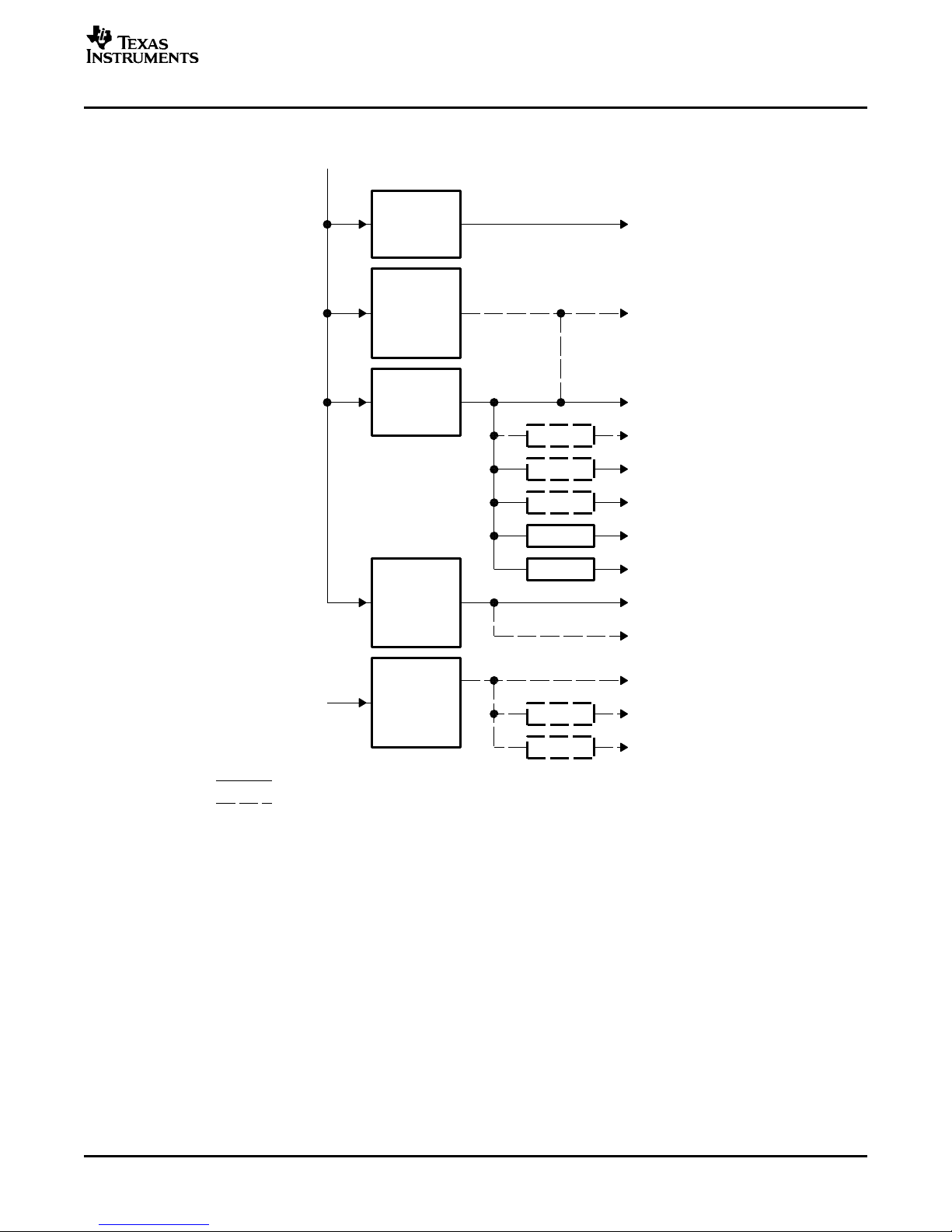
are also recommended for some other voltage planes. An overview of the recommended power supply
generation architecture is shown in Figure 7 .
The DVDD15 supply can be operated at either 1.5V or 1.8V. Operation at 1.8V will consume somewhat
more power than 1.5V operation but eliminates the need for a 1.5V supply. Most Ethernet PHYs that
support RGMII v2.0 operation support the HSTL interface at either 1.5V or 1.8V.
The optional power supplies are noted with dashed lines. These are power pins that can be connected
directly to VSS if the associated peripheral is not used and is disabled. If power supplies for SRIO or
RGMII are to be connected to VSS, care should be taken that all associated power for that interface must
be connected to VSS. Removing power from these interfaces will result in the inability to boundary scan
test these interfaces. Refer to the data manual for details.
Table 6. Power Supply Differences
Core Supply Voltage I/O Supply Voltages (Tolerances are +/-5%) Analog Supply Voltages
(Tolerances are +/-5%)
Device CVDD TOL DVDD33 DVDD18 DVDD15 DVDD12 PLL DDR2 SRIO
(SRIO) DLL
TCI6482 1.2V ±3% 3.3V 1.8V 1.5V 1.2V 1.8V 1.8V 1.2V
or
1.8V
TCI100 1.1V ±3% 3.3V N/A N/A N/A 3.3V N/A N/A
1.2V ±3%
14 TMS320TCI6482 Design Guide and Migration from TMS320TCI100 SPRAAC7B – April 2006
Submit Documentation Feedback
Page 15
www.ti.com
Switching
regulator
3.3 V
(RGMII)
Switching
regulator
1.5 V
Switching
regulator
1.8 V
1.5 V HSTL used
1.8 V
HSTL
used
Filter
Filter
Filter
Filter
Filter
Adjustable
switching
regulator
1.2 V
(SRIO)
Linear
regulator
1.2 V
Filter
Filter
Board voltage
(i.e. 5 V or 12 V)
DVDD33
DVDD15 (RGMII)
DVDD18
DVDDR (SRIO)
AVDLL1 (DDR2)
AVDLL2 (DDR2)
PLLV1
PLLV2
CVDD
DVDDRM (SRIO)
DVDD12 (SRIO)
AVDDA (SRIO)
AVDDT (SRIO)
DVDD18
Required
Optional
TCI6482
voltage planes
Power Supply
Filters on AVDLL1 and AVDLL2 are not needed if the DDR2 interface is not used.
The recommended filter circuit from Figure 7 is given in Figure 8 . The filter component shown is a from
Murata part. If a different part is cross-referenced, the frequency envelope must be considered. This
solution has been tested.
Figure 7. Power Supply Generation
SPRAAC7B – April 2006 TMS320TCI6482 Design Guide and Migration from TMS320TCI100 15
Submit Documentation Feedback
Page 16

www.ti.com
NFM18 CC22 2R1C3
0.1uF 560pF
1K 1 %
1K 1 %
DVDD18
VREFSSTL (DDR2)
DVDD15
VREFHSTL (RGM II)
0.1 u F
0.1 u F
1K 1 %
1K 1 %
0.1 u F
0.1 u F
Power Supply
Figure 8. Recommended Power Supply Filter
The reference voltages used for the SSTL (DDR2) and HSTL (RGMII) interfaces are intended to operate
at half the voltage supplied to those I/Os. This is done through a simple voltage divider as shown in
Figure 9 . More details on VREFSSTL can be found in: Implementing DDR2 PCB Layout on the
TMS320TCI6482 (SPRAAA9 ). Note that if the RGMII interface is not used and is disabled, VREFHSTL
can be connected to directly to VSS.
Figure 9. Reference Voltage Generation
7.2 Power Supply Sequencing [D]
16 TMS320TCI6482 Design Guide and Migration from TMS320TCI100 SPRAAC7B – April 2006
The recommended power sequence is described in the TCI6482 data manual. This is the sequence which
is used for manufacturing device test. Other sequences may work but have not been verified at this time.
Therefore, it is strongly recommended that this sequence be followed.
Submit Documentation Feedback
Page 17

www.ti.com
Although the power sequence has 3.3V I/O ramping before the core voltage, bus contention will not occur
in this case due to special circuitry that has been added that hold the 3.3V I/Os in tri-state during the
power ramp-up period.
There are multiple ways to generate a controlled power sequence. A microcontroller or PLD can be used
to control power supply sequencing. Alternatively, TI has power management products that can be used
such as the TPS3808 (http://focus.ti.com/lit/ds/symlink/tps3808g33.pdf ).
7.3 Voltage Plane Power Requirements
Power requirements are highly dependent on the usage of the device. This includes which peripherals are
used as well as the operating frequencies. In order to generate an estimate of the TCI6482 power for a
particular application, refer to the TMS320TCI6482 Preliminary Power Consumption Summary.
7.4 Power Supply Layout Recommendations
Core and I/O supply voltage regulators should be located close to the DSP (or DSP array) to minimize
inductance and resistance in the power delivery path. Additionally, when designing for high-performance
applications utilizing the C6000 platform of DSPs, the PCB should include separate power planes for core,
I/O and ground, all bypassed with high-quality low-ESL/ESR capacitors.
For VREFHSTL and VREFSSTL, one reference voltage divider should be used for both the TCI6482 and
the reference voltage input on the attached device. The same supply should also be used for the I/O
voltages between the 2 parts. The VREF resistor divider should be placed between the 2 devices and the
routes made as directly as possible with a minimum 20 mil wide trace. There should be a 2x trace width
clearance between the routing of the reference voltage and any switching signals.
The DLL signals (AVDLL1 and AVDLL2) can be routed using minimum 15 mil wide traces. There should
be a 2x trace width clearance between this and any switching signals.
The filter circuits should be placed as close to the corresponding TCI6482 power supply pin(s) as
possible. No digital switching signals should be routed near or directly under the filter circuits.
Power Supply
7.5 Voltage Tolerances, Noise, and Transients
The voltage tolerances specified in the datasheet include all DC tolerances and the transient response of
the power supply. These specify the absolute maximum and minimum levels that must be maintained at
the pins of the TCI6482 under all conditions. Special attention to the power supply solution is needed to
achieve this level of performance, especially the 3% tolerance on the core power plane (CVDD).
In order to maintain the 3% tolerance at the pins, the tolerance must be a combination of the power supply
DC output accuracy, the voltage drop from the supply to the load and the effect of transients. A
reasonable goal for the DC power supply output accuracy is 1.5%, leaving 1.5% for the transients. At 1.2V
a 3% tolerance is +/-36mV. This allows 18mV of DC accuracy from the output of the power supply and
another 18mV due to transients.
Power plane IR drop is another factor to consider, especially if there are multiple DSPs in a group on a
board. Power planes, even if no splits are present, have impedance. With large currents running across
the power planes the voltage drop must be considered. This same issue also applies to ground planes
with heavy currents.
7.5.1 Using Remote Sense Power Supplies
Use of a power supply that supports the remote sense capability allows the power supply to control the
voltage at the load. Special layout care must be used to keep this sense trace from being lost during PCB
layout. One solution is placement of a small resistor at the load and connecting the sense trace to the
voltage plane through it. If a group of DSPs on the board are supplied by a single core power supply, the
sense resistor should be placed at the center of this group. If a negative sense pin is supported by the
voltage regulator it should be handled in a similar way. An example of this type of implementation is
shown in Figure 10 .
SPRAAC7B – April 2006 TMS320TCI6482 Design Guide and Migration from TMS320TCI100 17
Submit Documentation Feedback
Page 18

www.ti.com
TCI6482
#1
VDD
VSS
TCI6482
#3
VDD
VSS
TCI6482
#2
VDD
VSS
TCI6482
#4
VDD
VSS
+SENSE
VSS
-SENSE
VOUT
0 ohms
0 ohms
VDD
VSS
REGULATOR
Routed as a signal
Routed as a signal
VCC VDD
VDD
VDD
VSSVSS
VSS VSS
VDD and VSS
routed as planes
VDD
VSS
Power Supply
Figure 10. Multiple DSP Remote Sense Connections
If the connection is between one DSP and one voltage regulator, there are voltage monitor pins that can
be used for this case. The monitor pins indicate the voltage on the die and therefore provide the best
remote sense voltage. Early TCI6482 data manuals have these pins grouped with their respective power
supplies. The voltage monitor pins are described in Table 7 .
Table 7. Die Voltage Monitor Pins
Voltage Plane Pin Number Description
CVDDMON N1 Die side core voltage monitor
DVDD33MON L6 Die side 3.3V (DVDD33) voltage monitor
DVDD18MON A26 Die side 1.8V (DVDD18) voltage monitor
These monitor pins should be connected directly to the positive side sense pin of the voltage regulator.
This may not be needed if the regulator used has a low impedance path between its VOUT and +SENSE
pins. Since the voltage regulator output could become unstable and drive to a high voltage if the positive
sense line does not receive the correct voltage it is recommended to place a 100 ohm resistor near the
DSP between the voltage plane and the monitor pin. If the VDDMON connection to the DSP is not present
for some reason the positive sense will still regulate to the proper voltage. If a negative sense pin is
provided by the regulator this should be connected to the GND plane near the DSP using a 0 ohm
resistor. The single DSP remote sense connections are shown in Figure 11 .
DVDD15MON F3 Die side 1.5V or 1.8V (DVDD15) voltage
monitor
18 TMS320TCI6482 Design Guide and Migration from TMS320TCI100 SPRAAC7B – April 2006
Submit Documentation Feedback
Page 19

www.ti.com
VDDMON
VDD
VSS
100 ohms
0 ohms
+SENSE
VSS
-SENSE
VOUT
Routed as a signal
Routed as a signal
REGULATORTCI6482
VDD
VDD
VSSVSS
VDD and VSS
routed as planes
7.5.2 Voltage Plane IR Drop
The voltage gradient (IR drop) needs to be considered whether or not a supply with the remote sense
capability is used. The DSPs closer to the supply will have a slightly higher voltage and the DSPs farther
from the supply will have a slightly lower voltage. This voltage differential can be minimized by making the
copper planes thicker or by spacing the DSPs across a wider area of the plane. Be sure to consider both
the core power plane(s) and the ground plane(s). The resistance of the plane can be determined by the
following formula:
R = rho * length / (width * thickness)
where rho is the resistivity of copper equal to 1.72E-8 ohm-meters. PCB layer thickness is normally stated
in “ounces”. One ounce of copper is about 0.012 inches or 30.5E-6 meters thick. The width must be
derated to account for vias and other obstructions. A 50mm wide strip of 1oz copper plane derated 50%
for vias will have a resistance of 0.57mohms per inch.
Power Supply
Figure 11. Single DSP Remote Sense Connections
7.6 Power-Supply Decoupling and Bulk Capacitors
In order to properly decouple the supply planes from system noise, place as many capacitors (caps) as
possible close to the DSP. Assuming 0402 caps, the user should be able to fit the number of capacitors
given in Table 9 . These caps need to be close to the DSP, no more than 1.25 cm maximum distance to be
effective. Ideally, these caps should be connected directly to the via attached to the BGA power pin.
Parasitic inductance limits the effectiveness of the decoupling capacitors; therefore the physically smaller
0402 capacitors are recommended. As with selection of any component, verification of capacitor
availability over the product’s production lifetime should be considered.
Proper capacitance values are also important. Small bypass caps (near 560 pF) should be placed closest
to the power pins. Medium bypass caps ( 100 nF or as large as can be obtained in a small package)
should be the next closest. TI recommends placing decoupling capacitors immediately next to the BGA
vias, using the “interior” BGA space and at least the corners of the “exterior”. The inductance of the via
connect can eliminate the effectiveness of the capacitor so proper via connections are important. Trace
length from the pad to the via should be no more than 10 mils and the width of the trace should be the
same width as the pad.
Larger caps can be placed further away for bulk decoupling. Large bulk caps should be furthest away (but
still as close as possible).
SPRAAC7B – April 2006 TMS320TCI6482 Design Guide and Migration from TMS320TCI100 19
Submit Documentation Feedback
Page 20

www.ti.com
Power Supply
7.6.1 Selecting Bulk Capacitance
There are 2 factors that need to be considered when selecting the bulk capacitance: the effective ESR for
the power plane capacitors, and the amount of capacitance needed to provide power during periods when
the voltage regulator cannot respond.
The overall impedance of the core power plane is determined by:
In Section 7.5 , it was suggested that the allowable voltage deviation allowed due to transient response is
18mV. The max transient current is estimated at 1.5A. So the impedance requirement is 18mV / 1.5Amps
= 12mohms. The power plane also has some impedance. An estimate of 2mohms will require a total
effective ESR of 10mohms. So the effective ESR of the bulk capacitors should not exceed this value.
Multiple bulk capacitors in parallel will help achieve this overall ESR.
The amount of the bulk capacitance is determined by the amount of time that the power regulator cannot
respond to the power demand and the amount of power that needs to be delivered during this time. The
maximum current change measurements have been made which show:
• Max current swing: 1.5Amp
The decoupling caps provide the immediate current through the transition but the bulk capacitors need to
supply this current until the voltage regulator can respond. A typical power regulator would have about a
10KHz bandwidth with a large capacitive load (needed to maintain the 18mV deviation). Assuming this
bandwidth and a 1.5A current transient, the minimum bulk capacitance needed is estimated at 1500uF. So
for this case the bulk capacitance needs to add up to 1500uF and create an effective ESR of 10mohms.
The capacitance may need to be further increased to cover temperature derating. Examples of suitable
capacitors are shown in Table 8 .
(Allowable Voltage Deviation due to Current Transients) / (Max Current)
Manufacturer Type Part Number C Vmax ESR QTY
AVX Tantalum TPSD337K004R0035 330uF 4V 35m Ω 5
KEMET Tantalum T530X687M004ASE005 680uF 4V 5m Ω 3
SANYO POS-CAP 2R5TPD1000M5 1000uF 2.5V 5m Ω 2
Capacitor selection should be done as shown above for the specific power supply implementation. If
multiple TCI6482 devices are used on a single core power plane the total capacitance could be reduced
per device if the expectation was that the transients would not occur on all devices simultaneously.
7.6.2 Recommended Capacitance
Recommended capacitor selection is given in Table 9 where it is also compared with the TCI100 capacitor
recommendations. The TCI6482 capacitor selection does not necessarily include power supply output
capacitance. Output capacitors are provided along with the power supply reference designs.
Voltage Capacitors Total Description Voltage Capacitors Total Description
Supply Capacitance Supply Capacitance
CVDD 10 * 560pF 2084uF 1.2V Core CVDD 1 * 330uF 333.2 uF Core
DVDD33 16 * 560pF 330uF 3.3V I/O DVDD 1 * 330uF 333.2 uF I/O
Table 8. Bulk Capacitor Examples
Table 9. Capacitor Recommendations
TCI6482 TCI100
20 * 100nF 32 * 100nF
3 * 680uF
2 * 22uF
24 * 100nF 32 * 100nF
1 * 330uF
20 TMS320TCI6482 Design Guide and Migration from TMS320TCI100 SPRAAC7B – April 2006
Submit Documentation Feedback
Page 21
www.ti.com
Table 9. Capacitor Recommendations (continued)
DVDD18 8 * 560pF 661.2uF 1.8V I/O
12 * 100nF PLLs
2 * 330uF DLLs
DVDD15 4 * 560pF 20.4uF RGMII
4 * 100nF
2 * 10uF
DVDD12 4 * 560pF 30.8uF SRIO
8 * 100nF
3 * 10uF
7.7 Discrete and Module Power Supply Solutions
TI can supply recommended power supply designs for discrete or module based solutions upon request.
7.8 Power Saving Options
7.8.1 Clock Gating unused Unused Peripherals
The TCI6482 can keep (or put) inactive/unused peripherals into a low power state. This capability is
discussed in the TCI6482 data manual. All peripherals that are not enabled are clock gated in order to
conserve power. After power-up, only those peripherals that are needed should be enabled.
Peripherals can also be disabled and put back into a lower power state. However, this should only be
done if no accesses to the peripheral will occur. Once a peripheral has been disabled it cannot be
re-enabled until after a reset.
I/O Buffers
7.8.2 Power Down Peripherals
Some peripherals that are disabled via the reset configuration can have their dedicated power planes be
connected to VSS. This achieves the lowest possible power dissipation. These peripherals are:
• SRIO: All SRIO power planes (DVDDRM, DVDDR, DVDD12, AVDDA, AVDDT) connect to VSS
• RGMII: DVDD15, VREFHSTL, RSV07, RSV08, RSV13, RSV14 connected to VSS
• DDR2: VREFSSTL, RSV11, RSV12 connect to VSS
Connecting these interfaces to VSS will prohibit the use of boundary scan to test the signals on these
interfaces.
For details on how to handle disabled peripherals refer to the peripheral specific chapters at the end of
this document.
7.8.3 General Power Saving Techniques
The following are some additional methods for reducing power:
• Lower frequency operation means lower power. The core and peripherals should be operated at the
lowest frequency that meets the user’s requirements.
• SRIO link power does not scale linearly with data rate. So a single 3.125Gbps link consumes less
power than three 1.25Gbps links. Generally, running fewer high speed links is more power efficient
than multiple slower links.
• RGMII operation at 1.5V will have lower power consumption than at 1.8V.
8 I/O Buffers
SPRAAC7B – April 2006 TMS320TCI6482 Design Guide and Migration from TMS320TCI100 21
Submit Documentation Feedback
Page 22

www.ti.com
Peripheral Section
8.1 PTV Compensated Buffers
The impedance of I/O buffers is affected by process, temperature and voltage. For some interfaces, these
impedance changes can make it difficult to meet specifications across the full range of these parameters.
For that reason, the TCI6482 uses PTV (process, temperature, voltage) compensated I/O buffers for
critical interfaces. The PTV compensation works by adjusting internal impedances to nominal values
based on external reference resistances. The interfaces that use PTV compensated I/O buffers and the
details on the reference resistances are given in Table 10 .
The resistors used can be standard 5% tolerance.
8.2 I/O Timings
The I/O timings in the TCI6482 data manual are given for the tester test load. These timings need to be
adjusted based on the actual board topology. In general, datasheet timings for interfaces that existed on
the TCI100 device have remained the same. However, some differences exist. Refer to the datasheet for
details. Since the TCI6482 is a completely new device, the nominal timings may be different than the
TCI100 and the I/O buffers may perform differently with a particular board topology. For these reasons, it
is highly recommended that timing for all high speed interfaces (with the exception of DDR and SRIO) on
a TCI6482 design be checked using IBIS simulations. For more details on performing IBIS simulations
see, Using IBIS Models for Timing Analysis (SPRA839 ).
The clock for many peripherals is generated by a divide down from the CPU core clock. Since the CPU
core clock is different than the TCI100, the divider and timings should be checked. This impacts the
McBSP, EMIFA and Timer Peripherals.
Table 10. PTV Compensated Interfaces
Interface Operating Voltage Reference Resistance
PCI 3.3V (DVDD33) 39 ohm resistor from RSV15 to GND
20 ohm resistor from RSV16 to DVDD33
RGMII 1.5V or 1.8V (DVDD15) 200 ohm resistor from RSV13 to GND
200 ohm resistor from RSV14 to DVDD15
DDR2 1.8V (DVDD18) 200 ohm resistor from RSV11 to GND
200 ohm resistor from RSV12 to DVDD18
8.3 External Terminators
The TCI6482 input/output (I/O) buffers have been modified for the new manufacturing process and have a
different output impedance than those of the TCI100. For boards designed with the TCI100, termination
resistor values should be checked by running IBIS simulations.
Series impedance is not always needed but is recommended for some interfaces to avoid
over-shoot/under-shoot problems. Check the recommendations in the Peripherals chapters and/or perform
IBIS simulations on the interface.
9 Peripheral Section
This section covers each of the TCI6482 peripherals/modules. This section is intended to be used in
addition to the information provided in the TCI6482 data manual, the Module Guides provided for each of
the peripherals and relevant application notes. The 4 types of documents should be used as follows:
• Data Manual: AC Timings, Register Offsets
• Module Guide: Functional Description, Programming Guide
• Applications Notes: System level issues
• This Chapter: Configuration, System level issues not covered in a separate application note,
Differences to the TCI100
Each peripheral section includes recommendations on how to handle pins on interfaces that are disabled
or for unused pins on interfaces that are enabled. Generally, if internal pull-ups or pull-downs are included
the pins can be left floating. Any pin that is output only can always be floated. If internal pull-ups and
22 TMS320TCI6482 Design Guide and Migration from TMS320TCI100 SPRAAC7B – April 2006
Submit Documentation Feedback
Page 23

www.ti.com
pull-downs are not included normally pins can still be floated with no functional issues for the device.
However, this normally does cause additional leakage currents which can be eliminated if external pull-ups
or pull-downs are used. When pull-ups or pull-downs are used the leakage current is approximately 100uA
per pin. When the pins are floating the leakage can be several milliamps. Although the recommendations
normally indicate using external pull-up resistors, pulll-down resistors can also be used. The leakage is the
same whether pull-ups or pull-downs are used. Connections directly to power or ground can be used only
if the pins can be guaranteed to never be configured as outputs. Use of boundary scan normally drives all
signals as outputs so direct connections to power or ground are not recommended if boundary scan is
used.
If a peripheral is selected (via the configuration strapping) but not enabled (via the peripheral configuration
register), then the I/Os can be treated the same as if the peripheral was not selected.
9.1 External Memory Interface (EMIFA)
Documentation for EMIFA:
• TCI648x DSP External Memory Interface (EMIF) Reference Guide (SPRU925)
• TCI6482 System Boot
• TCI6482 IBIS Model File
• Using IBIS Modes for Timing Analysis (SPRA839 )
9.1.1 Configuration of EMIFA
The EMIFA peripheral can be disabled using boot strapping options, as defined in the TCI6482 data
manual. If the EMIFA is enabled via boot strapping, it still needs to be enabled via software after a reset.
The clock to be used for EMIFA can either be supplied externally to the AECLKIN pin or can be generated
internally from the CPU core clock. The internally generated clock is referred to as SYSCLK4. After a
reset, SYSCLK4 is CPU core clock / 8. The SYSCLK4 divider can be changed via software register
accesses to PLL1.
If the EMIFA peripheral is not used, most EMIFA inputs can be left unconnected. Internal pull-up and
pull-down resistors are included on this interface so leakage will be minimal. Some EMIFA signals are
used for boot stapping options that are latched on the rising edge of POR (cold boot) or rising edge of
RESET (warm boot). If these signals are connected to other components it is recommnended to have 1K
pull-up or pull-down resistors in order to make sure the boot strapping options are properly latched.
If only a portion of the peripheral is used, control pins that are not used should be pulled to a valid state
and data pins that are not used can be left floating.
One of the boot modes is Boot over EMIF. In this mode, after reset the DSP immediately begins executing
from the base address of CE3 in 8-bit asynchronous mode.
Note that all synchronous memories connected to the EMIF should have clock enable low during device
power ramp and reset to avoid any inadvertent clocking of memories during power ramp and reset low.
This can be done by having a weak pull-down resistor (i.e. 10K) on the CKE signals.
Peripheral Section
9.1.2 System Implementation of EMIFA
Generally, series resistors should be used on the EMIFA signals to reduce over-shoot and under-shoot.
Generally acceptable values are 10, 22 or 33 ohms. To determine the optimum value simulations using
the IBIS models should be performed to check for signal integrity and AC timings.
Significant signal degradation can occur when multiple devices are connected on the EMIFA. Simulations
are the best mechanism for determining the best physical topologies and the highest frequency obtainable
with that topology. Generally, a synchronous interface is best from a performance standpoint and an
asynchronous interface has less performance but is easier to implement.
SPRAAC7B – April 2006 TMS320TCI6482 Design Guide and Migration from TMS320TCI100 23
Submit Documentation Feedback
Page 24

www.ti.com
Peripheral Section
9.1.3 TCI6482 EMIFA vs TCI100 EMIFA
Table 11 shows a comparison between the EMIFA features of the TCI6482 and the TCI100. The EDMA3
FIFO addressing mode is not supported so incrementing addressing is always used. This may require not
connecting lower address lines when attaching a device with a FIFO interface to the TCI6482 EMIFA
interface. The AC timings for the TCI6482 are similar to TCI100 but there are some differences. Refer to
the TCI6482 data manual to check AC timings.
Default condition (if enabled) Disabled Enabled
Programmable Synchronous Mode ü ü
(SBSRAM, ZBT, FIFO)
Asynchronous Mode (ROM, SRAM) ü ü
Addressable Ranges 64-bit: 8MB 64-bit: 8MB
ARDY features Can be disabled, polarity is programmable Always enabled and always active high
Support for late write SRAM ü
EMIF Boot Feature (executes from CE3 space) ü
SDRAM Mode ü
PDT Transfers ü
Clocking Options AECLKIN, AECLKIN,
Buffer Impedance 25 Ohms (data and AECLKOUT) 25 Ohms
Table 11. EMIFA Comparsion: TCI6482 vs TCI100
TCI6482 TCI100
32/16/8-bit: 4MB 32-bit: 4MB
16-bit: 2MB
8-bit: 1MB
Lack of ARDY timeout supported, can Wait states can lock up the interface
generate interrupt indefinitely
(1K ROM coopied to L2, then executed)
SYSCLK4 (internal divider) Core clock/4, Core clock/6
50 Ohms (control)
9.2 Host Port Interface (HPI) Memory Access
Documentation for HPI:
• TMS320TCI648x DSP Host Port Interface (HPI) User's Guide (SPRU874)
• TCI6482 System Boot
• TCI6482 IBIS Model File
• Using IBIS Modes for Timing Analysis (SPRA839 )
9.2.1 Configuration of HPI
The HPI interface is multiplexed with the PCI inteface. Selection between HPI and PCI is done via boot
strapping and latched by reset. If HPI is selected, a second boot strapping options selects the HPI bus
width as either 16 bit or 32-bit. The supported Boot over HPI option is selected by boot strapping as well.
Refer to the TCI6482 data manual for details on the strapping options.
Internally the HPI module is clocked by SYSCLK3, which is CPU core clock / 6. Therefore, the maximum
HPI timing is somewhat dependent on the CPU core clock frequency.
If neither HPI nor PCI is used, either PCI or HPI mode can be selected by the boot strapping and the
signals may be no-connects (as long as the peripheral is not enabled via the peripheral configuration
register). However, there may be additional power consumption when inputs are left floating. This can be
avoided by putting pull-up resistors on unused inputs.
If only a portion of the interface is used (i.e. HPI16 mode), control signals should be pulled to an
appropriate state and unused data signals can be left floating, although the power consumption will be
higher than if external pull-ups are used on these data signals.
TMS320TCI6482 Design Guide and Migration from TMS320TCI10024 SPRAAC7B – April 2006
Submit Documentation Feedback
Page 25

www.ti.com
9.2.2 System Implementation of HPI
Generally, series resistors should be used on the HPI signals to reduce over-shoot and under-shoot to
reduce EMI. Generally acceptable values are 10, 22 or 33 ohms. To determine the optimum value
simulations using the IBIS models should be performed to check for signal integrity and AC timings.
Default condition (if selected) Disabled Enabled
Supports 16 and 32-bit widths ü ü
Supports Boot over HPI ü ü
HCNTL[1:0] states 00: HPIC access 00: HPIC access
Support for SW polling of HRDY ü
Host can reset CPU core ü
Emulation Free/Soft bits ü
9.3 PCI Peripheral
Documentation for PCI:
• TMS320TCI648x DSP Peripheral Component Interconnect (PCI) User's Guide (SPRUE69)
• TCI6482 System Boot
• TCI6482 IBIS Model File
• Using IBIS Modes for Timing Analysis (SPRA839 )
Peripheral Section
Table 12. HPI Comparison: TCI6482 vs TCI100
TCI6482 TCI100
01: HPID access (auto inc) 01: HPIA access
10: HPIA access 10: HPID access (auto inc)
11: HPID access (fixed address) 11: HPID access (fixed address)
9.3.1 Configuration of PCI
The PCI interface is multiplexed with the HPI inteface. Selection between HPI and PCI is done via boot
strapping and latched by reset.
Due to other signal multiplexing, the enabling of PCI limits the Utopia interface to single PHY mode.
If PCI is selected, a second boot strapping option allows the PCI to get auto-initialized from an I2C ROM.
The PCI auto-initialization table, if used, needs to be installed at offset 0x400 in the I2C ROM. This allows
Boot over I2C ROM and PCI auto-initialization to both utilize the same EEPROM.
Another PCI strapping option selects between 33MHz and 66MHz PCI. This needs to be strapped based
on the PCI clock rate being used.
The Boot over PCI option is selected by boot strapping as well.
Refer to the TCI6482 data manual for details on the strapping options.
If neither HPI nor PCI is used, either PCI or HPI mode can be selected by the boot strapping and the
signals may be no-connects (as long as the peripheral is not enabled via the peripheral configuration
register). However, there may be additional power consumption when inputs are left floating. This can be
avoided by putting pull-up resistors on unused inputs.
If the peripheral is used but some control signals are not needed, these control signals should be pulled to
an appropriate state.
9.3.2 System Implementation of PCI
When the PCI interface is enabled the following PCI signals should have pull-up resistors: PFRAME,
PTRDY, PIRDY, PDEVSEL, PSTOP, PSERR, PPERR, and PINTA. Typical resistance values are
8.2Kohms but this is dependent on the number of loads. Refer to the PCI specification for details on
determining the optimal pull-up value.
SPRAAC7B – April 2006 TMS320TCI6482 Design Guide and Migration from TMS320TCI100 25
Submit Documentation Feedback
Page 26

www.ti.com
Peripheral Section
Operating PCI at 66MHz has tight timing requirements and should only be implemented for point-to-point
implementations.
The PCI specification gives sufficient guidelines that if followed, simulations are unnecessary. But if the
PCI specification guidelines are not followed or there is something unique in the implementation, IBIS
models are provided so simulations can be run.
9.3.3 TCI6482 PCI vs TCI100 PCI
Default condition (if selected) Disabled Enabled
PCI Conformance PCI Specification Revision 2.3 PCI Specification Revision 2.2
Operating Frequency 33MHz or 66MHz 33MHz
PCI Auto-Initialization Interface I2C ROM McBSP to SPI ROM
Target Window (outbound transfers) 32 8MB programmable target windows 1 fixed target window. Maximum of single
Target Window (inbound transfers) 6 base programmable windows unlimited 3 fixed base addresses
Supports Boot over PCI ü ü
Table 13. PCI Comparison: TCI6482 vs TCI100
TCI6482 TCI100
mapped to DSP memory space. 64MB transfer.
access range.
9.4 Multichannel Buffered Section Port (McBSP)
Documentation for McBSP:
• TMS320TCI648x DSP Multichannel Buffered Serial Port ( McBSP) Reference Guide (SPRU803)
• TCI6482 IBIS Model File
• Using IBIS Modes for Timing Analysis (SPRA839 )
9.4.1 Configuration of McBSP
McBSP0 and McBSP1 are multiplexed with the VLYNQ peripheral and a boot strapping option is used to
select between them. Another strapping option selects between McBSP1 and GPIO pins. After a reset,
software must enable the McBSP interface(s).
The McBSP module receives SYSCLK3 as its input clock, which runs at the CPU core clock / 6. The
McBSP port clocks can either be driven by an external clock (CLKS) or by an internal clock which is
derived from SYSCLK3. There is only one CLKS input which supplies both McBSP ports, but both ports
can individually be programmed to use internal or external (CLKS) clocks.
If the internal clock is selected, the minimum divisor is /2. For example, if the core clock is 1GHz then
SYSCLK3 is 166MHz and the maximum McBSP clock is 83MHz.
If a McBSP port is not used or some of the signals are not used, the pins can be left unconnected since
internal pull-ups/downs are included. The CLKS also has an internal pull-down so that it may be left
unconnected if not used.
9.4.2 System Implementation of McBSP
The maximum McBSP performance is achievable only when using source synchronous modes and
point-to-point connections. In this case, series resistance should be used to reduce over/under-shoot.
Generally acceptable values are 10, 22 or 33 ohms. To determine the optimum value simulations using
the IBIS models should be performed to check signal integrity and AC timings.
Multiple DSPs can be connected to a common McBSP bus using TDM mode. The additional loads will
require a reduction in the operating frequency. Also, the specific routing topology becomes much more
significant as additional DSPs are included. The way to determine the best topology and maximum
operating frequency are by performing IBIS simulations.
26 TMS320TCI6482 Design Guide and Migration from TMS320TCI100 SPRAAC7B – April 2006
Submit Documentation Feedback
Page 27

www.ti.com
.03" trace 1.0"/1.2" trace
CLKX0
or
FSX0
I/O
Model
PKG
Model
Micro
Strip
via
Strip
line
Strip
line
1.75"/2.0"tr ace
via
.03" trace
Strip
line
via
0.88"/1.0"tr ace
Micro
strip
Strip
line
1.75"/2.0"tr ace
via
.03"tr ace
Strip
line
via
0.88"/1.0"tr ace
Micro
strip
via
.03" trace
Strip
line
via
0.88"/1.0"tr ace
Micro
strip
This loadis
CLKX1or FSX1
This loadis CLKX2
or FSX2
This loadis CLKX3
or FSX3
Rterm
Micro
Strip
Micro
Strip
via
.03"tr ace .03" trace
600ohms
Strip
line
1.75"/2.0"tr ace
via
.03" trace
Strip
line
via
0.88"/1.0"tr ace
Micro
strip
This loadis CLKX4
or FSX4
Strip
line
1.75"/2.0"t race
via
.03"tr ace
Strip
line
via
0.88"/1.0"tr ace
Micro
strip
This loadis CLKX5
or FSX5
Strip
line
1.75"/2.0"tr ace
via
.03" trace
Strip
line
via
0.88"/1.0"tr ace
Micro
strip
This loadis CLKX6
or FSX6
Strip
line
1.75"/2.0"tr ace
via
.03"tr ace
Strip
line
via
0.88"/1.0"tr ace
Micro
strip
This loadis CLKX7
or FSX7
Strip
line
1.75"/2.0"tr ace
Rterm
Micro
Strip
Micro
Strip
via
600ohms
.03" trace
.03" trace
Peripheral Section
TI performed simulations on an 8 TCI6482 topology and the best routing topology for this is shown in
Figure 12 . This topology was able to operate with a 10MHz McBSP clock.
9.4.3 TCI6482 McBSP vs TCI100 McBSP
All the same McBSP modes are available on the TCI6482 as the TCI100. The differences between the
McBSP implementations are highlighted in Table 14 .
Default condition (if selected) Disabled Enabled
Number of McBSP ports 2 3
CLKS per McBSP port No, one CLKS for both ports Yes
Minimum clock period (CLKR/X) 6 * core clock period or 10ns (whichever is 6.67ns (based on internal speeds)
McBSP used for PCI auto-initialization No, I2C is used Yes, McBSP2 is used
9.5 Enhanced VCP
Documentation for VCP2:
• TMS320TCI648x DSP Viterbi-Decoder Coprocessor (VCP) Reference Guide (SPRUE09)
9.5.1 Configuration of VCP2
VCP2 needs to be enabled via software after a reset.
The VCP2 operates at CPU core clock / 3.
Figure 12. McBSP 8 Load Routing Topology
Table 14. McBSP Comparison: TCI6482 vs TCI100
TCI6482 TCI100
greater)
SPRAAC7B – April 2006 TMS320TCI6482 Design Guide and Migration from TMS320TCI100 27
Submit Documentation Feedback
Page 28

www.ti.com
Peripheral Section
9.5.2 TCI6482 VCP2 vs TCI100 VCP
The VCP2 is backwards compatible with the TCI100 VCP and it is enhanced in terms of performance
(data throughput), programmability and usability (bug fixes).
For details on migrating from VCP to VCP2, refer to the migration document listed above. For a summary
of the changes refer to Table 15 , Table 16 , and Table 17 .
Feature TCI100 VCP TCI6482 VCP2 Impact
VCP Clock CPU Core Clock/4 CPU Core Clock/3 Increased data rate
Branch Metric Resolution 7-bits 8-bits Increased dynamic range
FMAXI Only valid for (R + C) % = = 4 Valid for all frame lengths Feature usable for most frame
FMAXS lengths
FMINS
Y-Bit
Traceback Soft Decision RAM 1024 x 96 2048 x 64-bits Longer sliding windows in soft
Output FIFO RAM 32 x 64 64 x 64
Soft Decision Resolution 12-bits 8-bits
Hard Decision Ordering Oldest bit is in the MSB Programmable More flexibility
Debugging Features Pause Pause after each sliding Better visibility
Emulation Control NO Full Emulation Control Better visibility for System
HIU/EDMA Interface Shared HIU 64-bits Dedicated 64-bit bridge Reduced EDMA transfer time
RAMs Sleep Mode NO YES More Power Efficient
VCP Errata See the latest C6416 errata All critical errata corrected Usability improvement
Chip Support Library Available today Backwards compatible with Reduce migration effort
Table 15. VCP2 Summary of Changes on TCI6482
decision mode
window
Debug
sheet
C6416
Table 16. VCP2 Usage Change on TCI6482
Feature TCI100 VCP TCI6482 VCP2 Impact
Added in ¼ buffer events ½ buffer events ¼ buffer events and ½ buffer Flexibility
Memory Map Yes Yes - Modified Coding Migration
events
28 TMS320TCI6482 Design Guide and Migration from TMS320TCI100 SPRAAC7B – April 2006
Submit Documentation Feedback
Page 29
www.ti.com
Feature TCI100 VCP VCI6482 TCP2 Impact
VCPIC 3-5 Yes Modified Coding Migration
VCP Output Register 0-1 Yes Modified Coding Migration
(VCPSTAT0)
VCP Status Register 0 Yes Modified Coding Migration
(VCPSTAT0)
VCP error register (VCPERR) Yes Modified Coding Migration
VCP Endian Register Yes Modified Coding Migration
VCP Execution Register Yes Modified Coding Migration
(VPCEXE)
Peripheral Identification Yes Modified Coding Migration
Register (PID)
VCP Emulation Control Yes Modified Coding Migration
Register (VCPEMU)
9.6 Enhanced TCP
Documentation for TCP2:
• TMS320TCI648x DSP Turbo-Decoder Coprocessor (TCP) Reference Guide (SPRUE10)
9.6.1 Configuration of TCP2
TCP2 needs to be enabled via software after a reset.
The TCP2 operates at CPU core clock frequency / 3.
Peripheral Section
Table 17. VCP2 Register Changes on TCI6482
9.6.2 TCI6482 TCP2 vs TCI100 TCP
TCP2 is backwards compatible with TCP and it is enhanced in terms of performance (data throughput),
programmability and usability (bug fixes).
For details on migrating from TCP to TCP2, refer to the migration document listed above. For a summary
of the changes refer to Table 18 , Table 19 , and Table 20 .
Feature TCI100 TCP TCI6482 TCP2 Impact
TCP Clock CPU Core Clock/2 CPU Core Clock/3 Reduced decoding time
Prolong Reduction NO YES
Standalone Frame Size 5114 20730
Code Rates ½, 1/3,¼ 1/2, 1/3, ¼,¾, 1/5 Increased Programmability
Input Formats 8-bit, depends on code rate 6-bit, always assumes 1/5 Memory efficiency
Input Sign Not Programmable Programmable Offloads DSP CPU
Stopping Criterion SNR SNR or CRC BER improvement Offloads
Re-encoding NO YES Offloads DSP CPU
Log Equation Max Max and Max Programmability
Interleaver Load Before decoding Concurrently with first MAP Reduced latency
Hard Decision Ordering Oldest bit is in the MSB Programmable Programmability
Decoding Features Pause Pause after each MAP, Better visibility
Extrinsic Scaling NO YES, used in max-log-map Better BER
HIU/EDMA Interface Shared HIU 64-bits Dedicated 64-bit bridge Reduced EDMA transfer time
Memory Sleep Mode NO YES Power efficient
Table 18. TCP2 Summary of Changes on TCI6482
DSP CPU
Emulation Support
SPRAAC7B – April 2006 TMS320TCI6482 Design Guide and Migration from TMS320TCI100 29
Submit Documentation Feedback
Page 30

www.ti.com
Peripheral Section
Table 18. TCP2 Summary of Changes on TCI6482 (continued)
TCP Errata See errata sheet All critical errata corrected Usability improvement
Chip Support Library Available today Backwards compatible with Reduced migration effort
C6416
Table 19. TCP2 Usage Change on TCI6482
Feature TCI100 TCP TCI6482 TCP2 Impact
Memory Map Baseline Modified Coding Migration
Table 20. TCP2 Register Changes on TCI6482
Feature TCI100 TCP TCI6482 TCP2 Impact
TCPIC 0-11 YES YES-Modified Coding Migration
TCPIC 12-15 (Extrinsic Scaling NO YES Coding Migration
Registers)
TCPOUT 0 YES YES - Modified Coding Migration
TCPOUT 1- 2 NO YES Coding Migration
TCPEXE YES YES - Modified Coding Migration
TCPEND
TCPERR
TCPSTAT
Peripheral ID Register NO YES Coding Migration
9.7 GPIO/Device Interrupts
Documentation for GPIO/Interrupts:
• TMS320TCI648x DSP General-Purpose Input/Output (GPIO) User's Guide (SPRU725)
• TCI6482 IBIS Model File
• Using IBIS Modes for Timing Analysis (SPRA839 )
9.7.1 Configuration of GPIO/Interrupts
All GPIOs are multiplexed with other peripherals except for GP4 – GP7. The availability of the other
GPIOs is dependent on which peripherals are selected by boot strapping. For details on multiplexing
options and how to select GPIOs refer to the TCI6482 data manual.
All GPIOs that are selected by boot strapping, as well as GP4 – GP7, need to be enabled via software
before they can be configured. All GPIOs default to inputs.
All GPIOs can be used as interrupts and/or EDMA events. The GPIO module operates at CPU core / 6.
The fastest a GPIO can be switched is at half this rate. For example, at a CPU core frequency of 1GHz
the GPIO module clock is 166MHz and the max GPIO clock switching rate is 83MHz (or a max clock rate
of 41.5MHz).
All GPIOs except GP2 and GP12-GP15 have internal pull-down resistors, so these can be left
un-connected if not used. GP2 and GP12-GP15, if selected as GPIOs, can be left floating with a power
consumption penalty versus having external pull-up or pull-down resistors.
TMS320TCI6482 Design Guide and Migration from TMS320TCI10030 SPRAAC7B – April 2006
Submit Documentation Feedback
Page 31

www.ti.com
9.7.2 System Implementation of GPIO/Interrupts
It is recommended that GPIO’s used as outputs have a series resistance (22 or 33 ohms being typical
values). The value (or need) for the series resistor can be determined by simulating with the IBIS models.
If a GPIO needs to default to a particular state (low or high), an external resistor should be used. A pull-up
value of 1K is recommended to make sure that it over-rides the internal pull-down present on some
GPIOs.
GP0, GP1 and GP3 have output current ratings, Iol / Ioh, of 8mA / -8mA making them more suitable for
directly driving some LEDs as opposed to all other GP pins which have 4mA / -4mA output current ratings.
9.7.3 TCI6482 GPIO/Interrupt vs TCI100 GPIO/Interrupt
Default condition (if selected) Disabled Enabled
All GPIOs can generate Interrupts/EDMA Yes No, only GP0 and GP4-GP7
Events
9.8 Timers
Documentation for Timers:
• TMS320TCI648x DSP 64-Bit Timer User's Guide (SPRU818)
• TMS320C64x/C64x+ DSP CPU and Instruction Set Reference Guide (SPRU732 )
• Using IBIS Modes for Timing Analysis (SPRA839 )
Peripheral Section
Table 21. GPIO/Interrupt Comparison: TCI6482 vs TCI100
TCI6482 TCI100
9.8.1 Configuration of Timers
There are 2 timer peripherals: Timer0 and Timer1. Each timer needs to be enabled via software after a
reset before it can be used.
Each timer can be configured as a single 64--bit timer or as two 32--bit timers. There is an external timer
input signal and an external timer output signal for each timer. When a timer is used as two 32--bit timers,
the timer input and output can only be used with the lower 32-bit timer.
The timer module is clocked from CPU core clock frequency / 6. The timer input clock can be configured
to use the external timer input signal, the internal timer module clock (CPU core clock / 6) or as a gated
internal clock where the external timer input signal is used to gate the internal timer module clock.
If the external timer signals are not used, the pins can be left unconnected and the internal pull-downs will
bring the input to a low state.
In addition to the timer peripherals the CPU has a 64-bit free running counter that advances each CPU
clock after counting is enabled. The counter is accessed using two 32-bit read-only control registers in the
CPU. For more details on this timer, refer to the Time Stamp Counter Registers described in the
TMS320C64x/C64x+ DSP CPU and Instruction Set Reference Guide.
9.8.2 System Implementation of Timers
It is recommended that external timer signals use series resistance (22 or 33 ohms being typical values).
The value (or need) for the series resistor can be determined by simulating with the IBIS models.
External timer input signals are synchronized to the internal timer clock. Since the timer operates at CPU
core / 6, the timer input can be delayed from the timer input as much as one CPU core / 6 period.
SPRAAC7B – April 2006 TMS320TCI6482 Design Guide and Migration from TMS320TCI100 31
Submit Documentation Feedback
Page 32

www.ti.com
Peripheral Section
9.8.3 TCI6482 Timers vs TCI100 Timers
Default condition (if selected) Disabled Enabled
Number of Timer modules 2 3
Timer size (each) 1 @ 64-bits, 2@ 32-bits 32 bits
Watchdog functionality Yes No
Internal Timer clock frequency CPU core clock / 6 CPU core clock / 8
64 bit free running CPU counter Yes No
9.9 EDMA3
Documentation for EDMA3:
• EDMA v3.0 (EDMA3) Migration Guide for TMS320TCI648x DSP (SPRAAC1 )
• TMS320TCI648x DSP Enhanced DMA (EDMA3) Controller User's Guide (SPRU727 )
9.9.1 Configuration of EDMA3
The EDMA is enabled after a reset.
The EDMA is clocked at CPU core clock / 3.
Table 22. Timer Comparison: TCI6482 vs TCI100
TCI6482 TCI100
9.9.2 System Implementation
Configuration across the EDMA may not take affect immediately. In order to make sure that a peripheral
configuration has completed before accessing that peripheral it is recommended to setup an interrupt to
occur after the DMA has completed. After the interrupt is asserted the peripheral can be accessed.
9.9.3 TCI6482 EDMA3 vs TCI100 EDMA
The FIFO addressing mode of the EDMA3 channel controller is not supported by any of the peripherals on
the TCI6482 device, therefore, increment addressing mode should always be used. The migration
document referenced above gives a complete overview of the differences between the TCI6482 and the
TCI100 EDMA implementations.
9.10 Inter-Integrated Circuit (I2C)
Documentation for I2C:
• TMS320TCI648x DSP Inter-Integrated Circuit (I2C) Module User's Guide (SPRUE11)
• TCI6482 System Boot
• TCI6482 IBIS Model File
• Using IBIS Modes for Timing Analysis (SPRA839 )
• Philip's I2C Version 2.1 Specification:
http://www.semiconductors.philips.com/acrobat_download/literature/9398/39340011.pdf
9.10.1 Configuration of I2C
The I²C peripheral needs to be enabled via software before use. The input clock for the I²C module is core
clock / 6. There is a prescaler in the I²C module that needs to be setup to reduce this frequency to an
internal module clock of 7 to 12MHz.
If the I²C signals are not used, the SDA and SCL pins can be left floating. This does cause a slight
increase in power due to leakage which can be avoided by having pull-up resistors.
TMS320TCI6482 Design Guide and Migration from TMS320TCI10032 SPRAAC7B – April 2006
Submit Documentation Feedback
Page 33

www.ti.com
9.10.2 System Implementation of I2C
External pull-up resistors to 3.3V are needed on the I²C signals (SCL, SDA). The recommended pull-up
value is 4.7K ohms.
Multiple I²C devices can be connected to the interface but the speed may need to be reduced (400KHz is
the maximum) if many devices are connected.
9.11 Ethernet Media Access Controller
Documentation for Ethernet Media Access Controller (EMAC):
• TMS320TCI648x DSP EMAC/MDIO Module Reference Guide (SPRUE12)
• TCI6482 System Boot
• TCI6482 IBIS Model File
• Using IBIS Modes for Timing Analysis (SPRA839 )
9.11.1 Configuration of EMAC, MII, and MDIO
The EMAC interface MII/RMII/GMII signals are multiplexed with the Utopia interface, so only RGMII is
available if the Utopia interface is also used. When EMAC is enabled, the MDIO interface is always
enabled. Two other strapping bits are used to select the MII mode (MII, GMII, RMII, RGMII). The MII, GMII
and RMII share interface pins. The RGMII uses HSTL buffers and therefore has its own interface. There
are 2 sets of MDIO interfaces (LVCMOS and HSTL). If MII, GMII or RMII are selected the LVCMOS MDIO
interface (MDCLK, MDIO) is used. If RGMII is selected the HSTL MDIO interface (RGMDCLK, RGMDIO)
is used.
Even if EMAC is enabled by boot strapping, it still must be enabled via software before it can be
accessed.
The EMAC RMII , GMII, and RGMII require specific clock frequencies from PLL2 and therefore require
that CLKIN2 be 25MHz. In silicon version 2.0 and beyond RMII will no longer use the PLL2 output. MII
mode does not use the PLL2 output.
The RGMII interface HSTL buffers can either be operated at 1.5V or 1.8V. This is done by powering the
DVDD15 at either 1.5V or 1.8V. Operation at either of these voltages uses the same AC timings. 1.8V
operation consumes slightly more power than 1.5V but eliminates the need for creation of a separate 1.5V
supply. VREFHSTL is generated using a resistor divider from DVDD15 and therefore scales correctly.
In RGMII mode, the MDIO signals run at the same HSTL voltage as the RGMII signals.
For LVCMOS EMAC signals that are not used, these can either be left floating or pulled high. If left
floating some additional power is drawn due to leakage through the I/O buffers. If RGMII is not used, the
RGMII specific power planes should be connected to GND:
• VREFHSTL, DVDD15, RSV07, RSV08, RSV14. If RGMII power planes are connected to GND all
RGMII signals (including RGMDIO and RGMDCLK) should be no-connects.
CLKIN2 should not be left floating and should be pulled to GND if not needed.
Peripheral Section
9.11.2 System Implementation of MII
For termination, follow the switch/ PHY recommendations. If none are provided, it is recommended to use
series resistance termination. Typical values of 22 ohms or 33 ohms are normally adequate but IBIS
simulations can be used to verify the best value with a specific board implementation. All MII connections
should be point-to-point only.
9.11.2.1 RMII Implementation
In silicon version 1.1 the RMII interface supplies the 50MHz RMII reference clock as an output. This needs
to be connected to the reference clock input of the connected RMII device. There is no guaranteed timing
relationship between the CLKIN2 25MHz clock and this RMII reference clock. Therefore it cannot be
assumed that aligning CLKIN2 to multiple TCI6482 devices results in aligned RMII interfaces.
SPRAAC7B – April 2006 TMS320TCI6482 Design Guide and Migration from TMS320TCI100 33
Submit Documentation Feedback
Page 34

www.ti.com
Peripheral Section
9.11.2.2 RGMII Implementation
In silicon version 2.0, the RMII reference clock is an input. An external clock source should provide an
aligned reference clock to the TCI6482 RMII reference clock input and to the RMII device connected to the
other side of the interface.
Refer to the latest TCI6482 errata sheet for details.
The RGMII interface is compliant with the RGMII version 2.0 specification found at the following link:
http://www.hp.com/rnd/pdfs/RGMIIv2_0_final_hp.pdf
The electrical signaling is compatible to JEDEC specification JESD8-6:
http://www.jedec.org/download/search/jesd8-6.pdf
Although the JEDEC specification specifically details 1.5V HSTL signaling, the TCI6482 and most other
RGMII v2.0 devices support operation at 1.8V. Some devices support RGMII v1.3 (LVCMOS levels) but
not RGMII v2.0 levels. An application note on how to do voltage translation from the TCI6482 1.5V/1.8V
interface to an LVCMOS 2.5V/3.3V interface that operates at Gigabit speeds (125MHz) is given in the
Appendix A .
The RGMII interface operates at 125MHz and clocks data on both edges of the clocks. This connection
should be routed with high speed interface routing rules. The RGMII specification provides timing
information at both the receiver and the transmitter. The user must verify that the timing variations due to
board topology are not more than allowed by the RGMII specification. TCI6482 HSTL IBIS models are
provided to aid in this analysis.
The TCI6482 implements an internal delay (referred to as RGMII-ID in the RGMII specification) on the
transmit signals but not on the receive signals. So the connected device should use normal mode on the
transmit side (no delay) and internal delay mode on the receive side. If the connected device does not
support internal delay on the receive side, the proper delay needs to be created at the board level by
routing the RXC signal longer than the receive data signals. The RGMII specification calls for this trace
delay to be between 1.5nS and 2.0nS. Assuming a trace flight time of 170pS/inch, the clock should be
routed about 10.3 inches longer than the data and control. Flight time is dependent on board stackup and
this length should be adjusted for the flight time of the specific board design.
The TCI6482 silicon version 1.1 RGMII implementation relies on the in-band signaling as defined in
section 3.4.1 of the RGMII v2.0 specification in order to get link status, link speed and duplex information.
Until link status “UP” is indicated on this in-band signaling the TCI6482 will not transmit. It is therefore
required that the connected device support the transmission of all the in-band signaling and that this
feature is enabled before attempting to use the RGMII interface. Silicon version 2.0 offers a feature to
force the internal state of: link status, link speed, and duplex so that the in-band signaling will not be
required.
Some RGMII v2.0 devices have the MDIO interface implemented as 2.5V/3.3V LVCMOS. If RGMII is
selected on the TCI6482 only the HSTL MDIO interface is active. The circuit shown in Figure 13 has been
tested for this purpose. For more information and additional voltage translation options refer to the
following application note: Selecting the Right Level Translation Solution (SCEA035 )
34 TMS320TCI6482 Design Guide and Migration from TMS320TCI100 SPRAAC7B – April 2006
Submit Documentation Feedback
Page 35

www.ti.com
GND1
A1
A2
A3
GATE
B1
B2
B3
100K
0.1 u F
DVD D33
DV D D15
TC I6 4 8 2 RGMD C L K
TCI6 4 8 2 R G M DIO
2.5 V/3 .3 V M DCLK
150 15 0
2.5 V o r 3 .3V
2.5 V/3 .3V M D IO
SN 7 4 TV C3306
Peripheral Section
9.12 UTOPIA
Documentation for UTOPIA:
• TMS320TCI648x DSP Universal Test & Operations PHY Interface for ATM 2 (UTOPIA2) (SPRU726)
• TCI6482 System Boot
• TCI6482 IBIS Model File
• Using IBIS Modes for Timing Analysis (SPRA839 )
9.12.1 Configuration of UTOPIA
The Utopia interface is multiplexed with EMAC MII interfaces (except RGMII). So if Utopia is enabled, only
the RGMII interface is available for EMAC. Some Utopia address lines are multiplexed with PCI signals. If
PCI and Utopia are both enabled Utopia will operate in single PHY mode only. Boot strapping options are
used to select the state of the Utopia, EMAC and PCI interfaces. Refer to the TCI6482 data manual for
more details.
The Utopia RX and TX clocks are supplied externally and supports clock rates up to 50MHz.
If the Utopia interface is selected, software needs to enable it after reset release before it is accessible.
If the Utopia interface is not enabled, the input pins can be unconnected (floating) but this will result in
some additional power due to leakage. This power can be minimized by adding external pull-ups.
If the Utopia interface is enabled but some inputs are not used, external pull-ups or pull-downs are needed
to put these inputs into valid states.
Figure 13. HSTL to LVCMOS Translation
SPRAAC7B – April 2006 TMS320TCI6482 Design Guide and Migration from TMS320TCI100 35
Submit Documentation Feedback
Page 36

www.ti.com
Peripheral Section
9.12.2 System Implementation of Utopia
The Utopia interface can support multiple devices on the same bus using multi-PHY mode.
The 50MHz operation should not be an issue in a point-to-point connection. However, if multiple devices
are loaded on the bus, operation at 50MHz may not be possible. It is recommended to run IBIS
simulations to check the signal integrity and maximum operating frequency for a particular board topology.
9.12.3 TCI6482 Utopia vs TCI100 Utopia
The same Utopia module is in the TCI6482 as the TCI100. There should be no differences in the
implementations other than the method for configuring the peripheral.
9.13 VLYNQ
Documentation for VLYNQ:
• TCI6482 IBIS Model File
• Using IBIS Modes for Timing Analysis (SPRA839 )
9.13.1 Configuration of VLYNQ
The VLYNQ interface is multiplexed with both McBSP ports and some GPIO pins. It is selected on
power-up using the boot strap options. If it is selected, software must enable the interface after a reset.
The VLYNQ module logic operates off an internal clock of CPU core clock / 6. For the interface clock,
VLYNQ can be configured to use the VCLK pin as an input (external clock mode) or it can use internal
clock mode and the VCLK pin becomes an output. The internal clock mode operates from SYSCLK4
which is CPU core clock / 8 by default. This clock is programmable via PLL1. SYSCLK4 is used by both
VLYNQ and EMIFA so changing the divider will affect both of these interfaces. The maximum VLYNQ
operating frequency (both for internal and external clock modes) is 125MHz.
If the VLYNQ peripheral is not used or some of the signals are not used, the unused VLYNQ pins can be
left unconnected. Internal pull-ups/pull-downs will pull the pins to a static level.
9.13.2 System Implementation
VLYNQ is used in point-to-point connections only but it can be setup as a daisy chain between multiple
devices. For the TXD signals series resistance should be used to reduce over/under-shoot. Generally
acceptable values are 10, 22 or 33 ohms. All TXD terminals of a VLYNQ™ device connected to RXD
terminals of another VLYN device must have equal length point-to-point signal traces without stubs.
If VCLK is used as an output a series termination is required since this is also used as the VCLK input.
The series termination should be between 22 and 50 ohms. To determine the optimum series resistance
values simulations using the IBIS models should be performed to check signal integrity and AC timings.
For the VCLK routing, the circuit board should be designed using point-to-point connections without stubs
and enough bandwidth to support the maximum clock rate. If the VLYNQ clock rate is reduced by
changing the value of the “clkdiv” bits in the VLYNQ Control Register, the circuit board must be designed
to support half the maximum clock rate. This is necessary because the VLYNQ clock is only high for one
cycle of the pre-divided VLYNQ clock for all clkdiv values except zero. Figure 14 below shows an example
where the pre-divided VLYNQ clock rate is 125 MHz and the “clkdiv” bits are set to 100 binary. In this
example the VLYNQ clock rate is 25 MHz (high for 8 ns and low for 32 ns). However, the 8 ns high pulse
width requires the circuit board to be designed for 62.5 MHz.
36 TMS320TCI6482 Design Guide and Migration from TMS320TCI100 SPRAAC7B – April 2006
Submit Documentation Feedback
Page 37

www.ti.com
Peripheral Section
Figure 14. VLYNQ Clock Divider Example
If the VLYNQ clock is provided by an external source, the circuit board must be designed so transmission
line reflections do not generate glitches or invalid transitions of the VLYNQ clock. In most applications, the
external clock source should be connected to the CLK terminal of each VLYNQ device with two equal
lengths of etch. This configuration may require series termination resistors near the source of each clock
driver trace to prevent signal distortion. It may be possible to optimize timing on the VLYNQ interface by
allowing one VLYNQ device to receive the VLYNQ clock before the interconnected VLYNQ device. Refer
to Section 4 for more details related to VLYNQ timing. However, series termination may not be the best
method for terminating some configurations used to interconnect the external clock source to the two
VLYNQ devices.
The width of VLYNQ is adjustable down to 1 bit wide for a 3 signal interface (clock, tx data bit, rx data bit)
and has a max width of 4 bits.
9.14 Serial Rapid I/O (SRIO)
Relevant documentation for SRIO:
• TMS320TCI648x DSP Serial Rapid I/O User's Guide (SPRUE13)
• Implementing Serial Rapid IO PCB Layout on a TMS320TCI6482 Hardware Design (SPRAAB0 )
• TCI6482 System Boot
• TCI6482 SRIO/DDR Example Schematics
9.14.1 Configuration of SRIO
Since the SRIO port is not multiplexed with other peripherals, there is no boot strapping option to
enable/disable the SRIO port. SRIO, as with all peripherals, defaults disabled and must be enabled by
software before use.
There are 4 SRIO lanes. These can be configured for operation as a single 4x link or as 4 separate 1x
links.
SRIO requires a dedicated differential reference clock: RIOCLK, RIOCLK. Recommended frequencies for
this clock are 125MHz and 156.25MHz. The SERDES (serializer/deserializer) used in the SRIO solution
has a PLL which needs to be configured based on this reference clock and the desired link rate. Link rates
can be full, half or quarter rate relative to the PLL frequency. Refer to Table 23 for PLL multiplier settings
relative to link rate.
Reference Clock PLL Multipler Full Rate Half Rate Quarter Rate
125MHz 12.5 3.125Gbps not used not used
125MHz 10 2.5Gbps 1.25Gpbs not used
156.25MHz 10 3.125Gbps not used not used
156.25MHz 8 2.5Gpbs 1.25Gbps not used
Table 23. SRIO PLL Multiplier Settings
SPRAAC7B – April 2006 TMS320TCI6482 Design Guide and Migration from TMS320TCI100 37
Submit Documentation Feedback
Page 38

www.ti.com
Peripheral Section
It is possible to configure the TCI6482 to boot load application code over the SRIO interface. Boot over
SRIO is a feature that is selected using boot strapping options. For details on boot strapping options refer
to the TCI6482 data manual.
If the SRIO peripheral is not used the SRIO reference clock inputs and SRIO link pins can be left floating.
SRIO power planes can be connected to GND in order to reduce power. These power planes are:
• DVDDRM, DVDDR, DVDD12, AVDDA, AVDDT
If the SRIO peripheral is enabled but not all links are used, the pins of unused links can be left floating
and no terminations are needed.
9.14.2 System Implementation of SRIO
Refer to the Implementing Serial Rapid IO PCB Layout on a TMS320TCI6482 Hardware Design
(SPRAAB0 for information regarding supported topologies and layout guidelines.
Suggestions on SRIO reference clocking solutions can be found in Section 6.3.3 .
SRIO power planes and power filtering requirements are covered in Section 7.1 .
9.15 DDR2
Relevant documentation for DDR2:
• TMS320TCI648x DSP DDR2 Memory Controller User's Guide (SPRU894)
• Implementing DDR2 PCB Layout on the TMS320TCI6482 (SPRAAA9 )
• TCI6482 SRIO/DDR Example schematics
• JEDEC JESD79-2A: http://www.jedec.org/download/search/JESD79-2A.pdf
9.15.1 Configuration of DDR2
The DDR2 peripheral is enabled/disabled using boot strapping, as defined in the TCI6482 data manual. If
it is enabled, it still needs to be enabled via software after a reset.
The DDR2 clock is derived from PLL2, which uses the CLKIN2 reference clock. The DDR2 clock is 10x
the CLKIN2 frequency (25MHz CLKIN2 runs the DDR clock at 250MHz). The CLKIN2 range supports a
range of DDR2 operating frequencies, up to 533MHz (CLKIN2 = 26.7MHz). PLL2 is used for some of the
EMAC MII modes, specifically RMII, GMII, and RGMII. When these MII modes are selected CLKIN2 must
be 25MHz.
If the DDR2 peripheral is disabled all interface signals can be left floating since the input buffers are
disabled when the peripheral is disabled. CLKIN2 should have an external pull-down if not used. Note that
the DDR PLL voltages AVDLL1 and AVDLL2 are required to be at 1.8V even if DDR is not needed but the
filter circuit can be omitted.
If the DDR2 is operated in 16 bit mode, the upper DDR2 bi-directional pins should be pulled to valid
states. DSDDQS2, DSDDQS3, and DED[31:16] should have pull-up resistors to DVDD18. DSDDQS2z
and DSDDQS3z should have pull-downs to GND.
9.15.2 System Implementation of DDR2
Refer to the Implementing DDR2 PCB Layout on the TMS320TCI6482 (SPRAAA9 ) for information
regarding supported topologies and layout guidelines.
Suggestions on CLKIN2 reference clocking solutions can be found in Section 6.3.2 .
DDR power planes and power filtering requirements are covered in Section 7.1 .
9.16 JTAG/Emulation
Relevand documentation for JTAG/Emulation:
• 60-Pin Emulation Header Technical Reference, (SPRU655 )
• TMS320TCI6482 BSDL file
38 TMS320TCI6482 Design Guide and Migration from TMS320TCI100 SPRAAC7B – April 2006
Submit Documentation Feedback
Page 39

www.ti.com
9.16.1 Configuration of JTAG/Emulation
The JTAG interface can be used for boundary scan and emulation. The boundary scan implementation is
compliant to both IEEE 1149.1 and 1149.6 (for Serial RapidIO ports). Boundary scan can be used
regardless of the device configuration.
As an emulation interface, the JTAG port can be used in various modes:
• Standard emulation: requires only 5 standard JTAG signals
• HS-RTDX emulation: requires 5 standard JTAG signals plus EMU0 and EMU1. EMU0 and EMU1 are
bidirectional in this mode.
• Trace port: the trace port allows real-time dumping of certain internal data. The trace port uses the
EMU18:0 pins to output the trace data, however the number of pins used is configurable.
Emulation can be used regardless of the device configuration.
For supported JTAG clocking rates (TCLK) refer to the TCI6482 data manual. The EMU18:0 signals
can operate up to 166Mbps, depending on the quality of the board level implementation.
Any unused emulation port signals can be left floating.
9.16.2 System Implementation of JTAG / Emulation
For most system level implementation details, refer to the Emulation Header Technical Reference
document.
For a single DSP connection where the trace feature will not be used a non-buffered implementation can
be used if the connections are made per the SPRU655 application note. If the trace will be used, the
JTAG signals should be buffered and TCLK and RTCLK should be buffered separately.
If multiple DSPs are included on the board and a chained JTAG interface is desired, the suggested
implementation is to use a single 60 pin header with the following connections:
• Buffer and daisy chain the TDI and TDO
• Buffer and connect TCLK, TMS and TRST to all DSPs. RTCLK should be buffered separately from
TCLK.
• Connect EMU0 and EMU1 to all DSPs (do not buffer)
• Connect EMU18:2 to one of the DSPs (the one which will be traced)
No external pull-ups/downs are needed since there are internal pull-ups/downs on all emulation
signals.
The June 2004 version of the 60-Pin Emulation Header Technical Reference document indicates that
there should be a 100K ohm resistor between the TVD pin and the devices JTAG I/O voltage. This
value results in a significant voltage drop with some emulators, so the resistor should be 1K ohm
instead.
It is not recommended to add both a 60-pin header and a 14-pin header due to signal integrity
concerns. 60-pin to 14-pin adapters are available to allow connection to emulators that only support
the 14-pin connector.
Peripheral Section
9.16.3 TCI6482 JTAG/Emulation vs TCI100 JTAG/Emulation
Table 24. JTAG/Emulation Comparison: TCI6482 vs TCI100
TRST is fully asynchronous Yes No
Advanced Emulation pins 19 2
Trace support Yes No
9.17 Rake Search Accelerator (RSA)
Both RSAs can be enabled by software after a reset. The RSAs operate at CPU core clock speed.
SPRAAC7B – April 2006 TMS320TCI6482 Design Guide and Migration from TMS320TCI100 39
Submit Documentation Feedback
TCI6482 TCI100
Page 40

www.ti.com
Appendix A
Appendix A TCI6482 RGMII 1.5V/1.8V to 2.5V/3.3V Translation
The TCI6482 includes a variable voltage Reduced Gigabit Media Independent Interface (RGMII) for
connection to a gigabit-capable Ethernet switch or PHY. The TCI6482 interface may be configured
to run at either 1.5V or 1.8V I/O; controlled directly by the voltage applied to the DVDD15 pins of
the device (see device data manual). These rails are complaint with the RGMII specification;
however, in practice it has been found that in many cases a level translation is required between
industries offering for Ethernet switch connections, which are slightly slower in migration to these
lower voltage nodes.
Voltage translation of the RGMII interface is a somewhat complicated task, insomuch as the
interface must be level-translated but still support dual-data rates at up to 125MHz operation. This
can be very difficult to achieve using standard LVCMOS-type buffers for two reasons. Firstly, such
buffers often add up to 4ns propagation delay to the buffered signals, making timing margins
exceptionally small at the 125MHz rate. Secondly, such buffers often provide little to no guarantee
of relative propagation delays across buffers in the same device and further specify all timings with
only a single output switching, which is not realistic in a gigabit Ethernet application.
As an alternative to the LVCMOS type buffers, a good solution can be found using TVC-type
buffers or CBT buffers in a TVC configuration. Texas Instruments has an excellent application note
describing the configuration (SCEA035A ). An example of this application is shown in Figure A-1
using a CBT3245 in a TVC voltage-clamp configuration. The CBT3245 is an 8 in/out buffer, making
it a nice fit for the 6 lines requiring translation in a single direction of a gigabit Ethernet application.
Using this solution, two CBT3245s can be used (one for transmit, one for receive) to complete the
translation.
Figure A-1. RGMII Voltage Level Translation Circuit
40 TMS320TCI6482 Design Guide and Migration from TMS320TCI100 SPRAAC7B – April 2006
Submit Documentation Feedback
Page 41

www.ti.com
Appendix A
The CBT and TVC families of buffers are excellent in this application. Both are simple FET
switches, which offer sub-ns propagation delays. Because each FET switch is independent; the
relative delays are matched very closely because process variations affect all switches equally.
Unlike LVCMOS buffers however, these switches offer no additional current drive, however since
gigabit Ethernet connections are simple point-point connections this is not a concern.
As a FET switch, the circuit in either the TVC or CBT application is the same. A single in/out pair is
chosen to set the voltage clamp voltage to 1.8V on the TCI6482 side (1.5V could also be used if
that voltage is used for the TCI6482 RGMII interface). Because all the gates of the CBT/TVC in/out
pairs are connected, this sets the clamp voltage for all the other pairs of ins/outs because VGS for
the FET is fixed. Note that the buffer itself is powered using a 3.3V supply however. This is
necessary to establish a voltage at least 1V greater than the low-side clamp voltage (18.V + 1V =
2.8V in this case).
The configuration shown above is technically a bidirectional solution; though gigabit Ethernet by its
definition is unidirectional. When driving from the TCI6482 to the switch/PHY, signals will vary from
0V to 1.5V/1.8V. At the low (0V) voltage level, the FET is turned on and both sides of the buffer
thus see a low level. When a 1.5V/1.8V logic high is applied, the FET is turned off because this
voltage matches (nearly) the voltage applied to the gate. In this case, the pullups on the high
voltage side (switch/PHY side) of the buffer pull the output to the high-side rail. Thus, in both cases
the logic levels on both sides of the buffer match to their respective rails. The application circuit
shown above is shown for the TCI6482’s transmit direction; that is; from the TIC6482 to the switch.
In the receive direction, the application circuit is the same except that the pullups to the 2.5V side of
the buffer, the switch/PHY side that is, are not needed and should be omitted. In this case, pullups
to 1.5V/1.8V are not required, as the buffer will act as a clamp and hold the output voltage to the
1.5V/1.8V level, thus providing the translation directly.
The values for the pullups on the high-voltage side of the CBT/TVC buffer are important. The basic
trade-off that needs to be made is finding a value that is strong enough to pull to the high-side rail
quickly to produce a good low-high edge rate (recall this is when the FET turns off), but is not too
strong so as to not allow the low side to pull the output to a level below the VIL specification of the
switch/PHY device when a low is driven (and the FET is on). In practice, a 150 Ohm pullup is a
good solution.
Shown below are several SPICE plots showing the characteristics of this solution. Figure A-2
shows the relationship between VIN and VOUT that establishes the clamping to the low voltage
side rail even when the input voltage exceeds that rail. Figure A-3 shows a square wave driven
from each side and the resulting outputs. Note in all cases the extremely low propagation delay and
good edge rates that result with this solution.
SPRAAC7B – April 2006 TMS320TCI6482 Design Guide and Migration from TMS320TCI100 41
Submit Documentation Feedback
Page 42
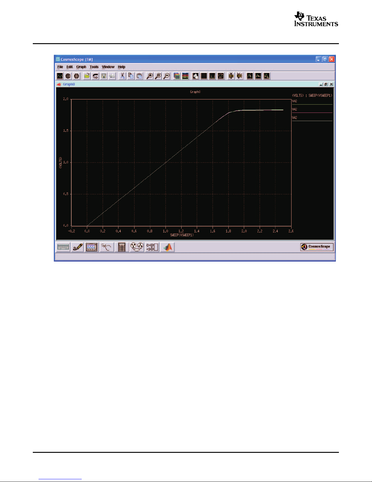
www.ti.com
Appendix A
Figure A-2. VOUT vs VIN
Setup for V
vs.V
OUT
plot: B2 was swept from 0 to 2.5v in 0.1v steps and the waveform at A2 was
IN
observed. A 1Meg resistor to GND was connected at A2.
42 TMS320TCI6482 Design Guide and Migration from TMS320TCI100 SPRAAC7B – April 2006
Submit Documentation Feedback
Page 43

www.ti.com
Appendix A
Figure A-3. 125MHz Signal from A2 to B2 and From B3 to A3
SPRAAC7B – April 2006 TMS320TCI6482 Design Guide and Migration from TMS320TCI100 43
Submit Documentation Feedback
Page 44

IMPORTANT NOTICE
Texas Instruments Incorporated and its subsidiaries (TI) reserve the right to make corrections, modifications,
enhancements, improvements, and other changes to its products and services at any time and to discontinue
any product or service without notice. Customers should obtain the latest relevant information before placing
orders and should verify that such information is current and complete. All products are sold subject to TI’s terms
and conditions of sale supplied at the time of order acknowledgment.
TI warrants performance of its hardware products to the specifications applicable at the time of sale in
accordance with TI’s standard warranty. Testing and other quality control techniques are used to the extent TI
deems necessary to support this warranty. Except where mandated by government requirements, testing of all
parameters of each product is not necessarily performed.
TI assumes no liability for applications assistance or customer product design. Customers are responsible for
their products and applications using TI components. To minimize the risks associated with customer products
and applications, customers should provide adequate design and operating safeguards.
TI does not warrant or represent that any license, either express or implied, is granted under any TI patent right,
copyright, mask work right, or other TI intellectual property right relating to any combination, machine, or process
in which TI products or services are used. Information published by TI regarding third-party products or services
does not constitute a license from TI to use such products or services or a warranty or endorsement thereof.
Use of such information may require a license from a third party under the patents or other intellectual property
of the third party, or a license from TI under the patents or other intellectual property of TI.
Reproduction of information in TI data books or data sheets is permissible only if reproduction is without
alteration and is accompanied by all associated warranties, conditions, limitations, and notices. Reproduction
of this information with alteration is an unfair and deceptive business practice. TI is not responsible or liable for
such altered documentation.
Resale of TI products or services with statements different from or beyond the parameters stated by TI for that
product or service voids all express and any implied warranties for the associated TI product or service and
is an unfair and deceptive business practice. TI is not responsible or liable for any such statements.
Following are URLs where you can obtain information on other Texas Instruments products and application
solutions:
Products Applications
Amplifiers amplifier.ti.com Audio www.ti.com/audio
Data Converters dataconverter.ti.com Automotive www.ti.com/automotive
DSP dsp.ti.com Broadband www.ti.com/broadband
Interface interface.ti.com Digital Control www.ti.com/digitalcontrol
Logic logic.ti.com Military www.ti.com/military
Power Mgmt power.ti.com Optical Networking www.ti.com/opticalnetwork
Microcontrollers microcontroller.ti.com Security www.ti.com/security
Telephony www.ti.com/telephony
Video & Imaging www.ti.com/video
Wireless www.ti.com/wireless
Mailing Address: Texas Instruments
Post Office Box 655303 Dallas, Texas 75265
Copyright 2006, Texas Instruments Incorporated
 Loading...