


SPRU011
~
~
~
Family
Developtnent
Support
Reference
S320
.
Guide
."
TEXAS
INSTRUMENTS

TMS320 Fatnily
Developtnent
Support
Reference
Guide
TEXAS
•
INSI:'RUMENTS

IMPORTANT
Texas
Instruments (TI)
reserves
the right
device specifications identified in this publication
its customers to obtain the latest version
NOTICE
to
make
changes in the devices or the
without
of
device specifications
notice. TI advises
to
verify,
before placing orders, that the information being relied upon by the customer
is
current.
In the absence
of
written agreement
to
the contrary,
TI
assumes no liability for
TI applications assistance, customer's product design, or infringement
ents or copyrights
devices described herein. Nor does
either express or
intellectual property right
chine, or process in which such semiconductor devices might
of
third parties by or arising from use
TI warrant or represent that any license,
implied,
Copyright © 1986, Texas Instruments Incorporated
is
granted under any patent right, copyright, or other
of
TI
covering or relating
to
any combination, ma-
of
semiconductor
be
or are used.
of
pat-


Quick
Reference
for
This
Document
TITLE
Introduction
The
TMS320
ROM Codes
Quality and Reliability
TMS320
Software Support Products
Hardware Development Tools
RTCTMS320
TMS320
TMS320
TMS320
Digital Signal Processor Family
Development Support Products
Seminar and Workshops
Documentation Support
University Program
Third-Party Support
TITLE
SECTION
1
2
3
4
5
6
7
8
9
10
11
APPENDIX
TMS320
TI Factory Repair and Exchange Policy
TI Program License Agreement
Product Order Information
A
B
C
v

vi

Contents
Section
1
Introduction
1.1
How
to
Use
This Manual
2
The
TMS320
2.1
First-Generation Devices
2.2 Second-Generation Devices
Typical Applications
2.3
3
ROM
Codes
4
Quality
4.1
Reliability Stress Tests
5
TMS320
6
Software
6.1
TMS320 Macro Assembler/Linker
TMS320 Simulator
6.2
6.3 SoftWare
Digital Filter Design Package (DFDP)
6.4
Digital Signal Processing Software Library
6.5
TMS320 Bell 212A Modem Software
6.6
Digital
and
Reliability
Development
Support
Development System (SWDS)
Signal
Support
Products
......
Processor
Products
.
Family
Page
1-1
1-3
2-1
2-4
2-9
2-12
3-1
4-1
4-2
5-1
6-1
6-2
6-5
6-7
6-10
6-13
6-15
7
Hardware
7.1
TMS320 Evaluation Module (EVM)
7.1
.1
System Configuration
7.1.2 Communication
7.1.3 Debugging
7.1.4 Equipment List
TMS320 Emulator (XDS)
7.2
7.2.1
7.2.2 Communication
7.2.3 Debugging
7.2.4 Equipment List
7.3
7.3.1
7.3.2 Customer Upgrade
7.4
7.4.1
7.4.2 Equipment List
7.5
System Configurations
TMS320 XDS Upgrade Program
TI
TMS320 Analog Interface Board
System Configuration
TMS320 DSP Design Kit
Development
.....
.....
Factory Upgrade
Tools
.
(AlB)
7-1
7-2
7-5
7-6
7-7
7-8
7-9
7-13
7-15
7-15
7-16
7-17
7-19
7-20
7-21
7-22
7-23
7-25
vii

8 RTC
8.1
8.2
8.3
TMS320
TMS320 Product Seminar
DSP
Design Workshops
RTC
locations . . . . .
Seminar
and
Workshops
8-1
./.
8-2
8-3
8-4
9TMS320
9.1
Produtt Descriptions and Product Bulletins
9.2 User's Guides
9.3
Data
9.4
DSP
9.4.1
9.4.2
9.4.3 Companding Routines for the
9.4.4 Floating-Point Arithmetic
9.4.5
Documentation
Support
...............
Sheets
Applications Book
Implementation
Fast
Fourier Transform Algorithms with the TMS32020 9-7
................
of
............
FIR/IIR Filters with the TMS32010/TMS32020
..........
TMS3201 0/TMS32020
with
the TMS3201 0 9-7
Floating-Point Arithmetic with the TMS32020
9-1
9-2
9-3
9-4
9-5
9-6
9-7
9-7
9.4.6 Precision Digital Sine-Wave Generation with the TMS3201 0 9-S
9.4.7 Matrix Multiplication with the TMS3201 0
9.4.8 Interfacing to Asynchronous Inputs with the TMS3201 0
9.4.9 Interfacing External Memory to the TMS3201 0
9.4.10 Hardware Interfacing to the TMS32020
9.4.11 TMS32020 and MC6S000 Interface
9.4.12 Telecommunications Interfacing to the TMS3201 0
9.4.13 Digital Voice
9.4.14 Implementation
Echo
Canceller with a TMS32020
of
Data
Encryption Standard Using TMS3201 0 9-
9.4.15 32-kbit/s ADPCM with the TMS3201 0
9.4.16 A Graphics
9.4.17
Control
9.5 University Textbooks
9.5.1
9.5.2
9.5.3
DFT/FFT and Convolution Algorithms 9-13
Digital Filter Design
Practical Approaches to Speech Coding
Implementation Using the TMS32020 lind TMS34061 9-11
System
Compensation
and
...........
..........
9.5.4 A Practical Guide to Adaptive Filter Design
9.5.5 A
9.6 Technical Articles
9.7
9.S
9.8.1
9.9 TMS320
Digital Signal Processing laboratory Using the TMS3201 0 9-
......................
TMS320 Quarterly Newsletter
TMS320
DSP
Bulletin Board Service
How to Access the TMS320
DSP
Hotline
............
...............
DSP
Bulletin Board Service
and
TMS32020
9-8
9-8
9-9
9-9
......
9-9
9-
.......
............
9~
9-11
Implementation with TMS3201 0 9-12
9" 13
9-14
9-14
....
9-14
9-16
9-23
............
9-24
9-24
'.
. . . . . . . 9-27
10
10
10
15
10
TMS320
10.1
TMS320' Hardware/Software Available to Universities
10.2
DSP
11
TMS320
11.1
Allen Ashley
11.2
Atlanta Signal Processors, Inc. (ASPI)
Avocet
11.3
11.4
Bedford
Burr Brown Corp.
11.5
11.6
Computalker
11.7
Crowell, Inc.
Cybernetic Micro
11.8
11.9
Daisy Systems Corp.
University
Program
Station Recommendations . . . . . .
Third-Party
.........
Systems,
Support
.
Inc.
Research
. . . .
Systems
viii
10-1
10-2
10-2
11-1
11-2
11-3
11-5
11-5
11-6
11-S
11-9
11-10
11-10

11
.10 Dalanco Spry
11.11 Digital Audio Corp. .
11.12 Digital
11.13 Digital Sound Corp.
11.14
DSP Technology Corp.
11
.15 Forth, Inc.
11.16
Gas
11.17 Hewlett-Packard
11
.18 Hyperception
11.19 Kontron Electronics
11.20 Loughborough Sound Images Ltd.
11.21 Microcraft Corp.
11.22 Microstuf,
11.23
PH
11.24 Pacific Microcircuits Ltd.
11.25 Pratica
11.26
Racal
11.27 Sentry Test
11.28 Signal Technology, Inc. (STI)
11.29 Signix Corp.
11.30 SIGnology, Inc. •
11.31
SKY Computers, Inc.
11.32 TelePhoto Communications
11.33 Televic
11.34
Texas
11.35 Thorn EMI Electronics
11.36
TIAC Manufacturing, Inc.
11.37 Valid Logic Systems
11
;38 Votan
11
.39 Whitman Engineering, Inc.
11.40 Third-Party Address, Phone, and Product Support List
11.41 Third-Party Consultants
11
.42 Trademarks
Signal Processing Software, Inc. (DSPS)
Light Software
Associates
SRL
Microelectronics Systems Ltd.
........
Instruments, Inc.
........
..............
Inc.
....
....
..........
Systems
......
.....................
.....
...
..........
.
.
.
.
.
.
............
.
.
.
.
11-11
11-12
11-12
11-13
11-14
11-15
11-15
11-16
11-18
11-19
11-19
11-20
11-21
11-21
11-22
11-25
11-25
.
11-26
11-26
11-27
11-28
11-29
11-33
11-34
11-35
11-36
11-37
11-38
11-38
.
.
11-39
11-41
11-47
11-49
A
B
C
Product
Texas
Texas
Instruments
Instruments
Order
Information
Factory
Program
Repair
License
and
Exchange
Agreement
Policy
A-1
8-1
C-1
ix

III
ustrations
Figure Page
1-1. TMS320 Family Development Support . . . . . . . . . . . . . . . . . . . . . . . . .
2-1. The TMS320 Family Roadmap . . . . . . . . . . . . . . . . . . . . . . . . . . . . . . .
2-2. TMS32010, TMS3201 0-14, TMS3201 0-25, TMS320C1 0, TMS320C1
2-3. TMS320C15/E15, TMS320C15-25 Block Diagram
2-4. TMS32011 Block Diagram . . . . . . . . . . . . . . . . . . . . . . . . . . . . . . . . . .
2-5. TMS320C17 /E17, TMS320C17 -25 Block Diagram . . . . . . . . . . . . . . .
2-6. TMS32020 Block Diagram . . . . . . . . . . . . . . . . . . . . .
2-7.
3-1.
5-1. TMS320 Development Product Integration . . . . . . . . . . . . . . . . . . . . .
5-2. Typical TMS320 Application Development Flow . . . . . . . . . . . . . . . . .
6-1.
6-2. Linked Assembly
6-3. Simulator Screen Example . . . . . . . . . . . . . . . . . . . . . . . . . . . . . . . . . . .
6-4. SoftWare Development System (SWDS)
6-5. SWDS Screen Example .
6-6. Digital Filter Design Package (DFDP) . . . . . . . . . . . . . . . . . . . . . . . . .
6-7. DFDP Plot Examples
7-L
7-2. TMS32020/C25 Evaluation Module (EVM) . . . . . . . . . . . . . . . . . . . . .
7-3. TMS320
7-4. TMS320 EVM/Single-User System . . . . . . . . . . . . . . . . . . . . . . . . . . . .
7-5. TMS32010
7 -6. TMS320C10 Emulator (XDS/22) . . . . . . . . . . . . . . . . . . . . . . . . . . . . .
7-7. TMS320C25 Emulator (XDS/22) . . . . . . . . . . . . . . . . . . . . . . . . . . . . .
7 -8.
7-9.
7-10. TMS320 XDS/Single-User System
7-11
7-12. TMS320C10 XDS/22 Display Example
7 -13. XDS Upgrade Configurations . . . . . . . . . . . . . . . . . .
7-14.
7-15.
7 -16.
7-17.
11-1.
11-2. Burr Brown's VMEdsp
11-3. Burr Brown's VMEdsp MPV960 Analog Input
11-4. Dalanco Spry's Model 1 0 Digital Signal Processor . . . . . . . . . . . . . . . .
11-5. HP
11-6. Pacific Microcircuits' PD32HC01 Interface IC . . . . . . . . . . . . . . . . . . .
11-7. Pacific Microcircuits' SuPPort 320
11-8. SIGnology's SP-20 DSP Development/Measurement System . . . . . . .
11-9. SKY320-PC
11-10.SKY320-Q
11-11. SKY Challenger VMEbus DSP Board . . . . . . . . . . . . . . . . . . . . . . . . . .
'1-12.
Block Diagram . . . . . . . . . . . . . . . . . . . . . . . . . . . . . . . . . . . . . . . . . . . .
TMS320C25 Block Diagram
TMS320 ROM Code Flowchart . . . . . . . . . . . . . . . . . . . . . . . . . . . . . .
Assembly
TMS32010 Evaluation Module (EVM)
TMS320C25 Emulator Target Connector . . . . . . . . . . . . . . . . . . . . . . .
TMS320 XDS Host Computer Mode
..
TMS320 XDS Multiprocessor Mode . . . . . . . . . . . . . . . . . . . . . . . . . . .
TMS320 Analog Interface Board . . . . . . . . . . . . . . . . . . . . . . . . . . . . .
TMS320
TMS320 AI B Adaptor Board . . . . . . . . . . . . . . . . . . . . . . . . . . . . . . . . .
TMS320
ASPI's Algorithm Development Package (ADP) . . . . . . . . . . . . . . . . . .
TI-Speech Development System . . . . . . . . . . . . . . . . . . . . . . . . . . . . . .
with
a Single-Source Module . . . . . . . . . . . . . . . . . . . . . . . .
with
Multiple-Source Modules . . . . . . . . . . . . . . . . .
.........................................
EVM
Host Computer Mode .
EVM
with
Audio Cassette Interface . . . . . . . . . . . . . . . . . .
AlB
System Configuration
DSP
Design Kit
SPV1
64285S Emulation Subsystem . . . . . . . . . . . . . . . . . . . . . . . . . . . .
DSP
Board . . . . . . . . . . . . . . . . . . . . . . .
DSP
Board
...................................
.......................................
.....................................
00
Board . . . . . . . . . . . . . . . . . . . . . . . . .
DB01
.......................................
.......................
...........................
..
. . . . . . . . . . . . . . . . . . . . . . .
............................
..............................
...........................
.............................
and
Development Board . . . . . . .
...............
...
. . . . . . . . . . .
..
. . . . . . . . . . . .
DSP
Board . . . . . .
..
. . . . . . . . . . .
0-25
..
..
..
"
..
..
..
..
..
..
..
..
..
"
..
..
..
..
..
..
..
..
..
..
..
..
..
..
..
..
..
..
..
..
..
..
..
1-2
2-2.
2-6
2-6
2-8
2-8
2-11
2-11
3-2
5-2
5-3
6-3
6-4
6-6
6-8
6-9
6-10
6-12
7-3
7-4
7-5
7-5
7-6
7 -10
7-11
7 -12
7-13
7-14
7-14
7-15
7 -18
7-21
7-22
7 -'23
7-26
11-4
11-7
11-8
11-11
11-17
11-23
11-24
11-29
11-31
11-32
11-33
11-36
x

A-1. TMS320 Device Nomenclature . . . . . . . . . . . . . . . . . . . . . . . . . . . . . . .
A-2. TMS320 Development Tool Nomenclature . . . . . . . . . . . . . . . . . . . . . .
Tables
..
..
A-5
A-6
Table
2-1.
TMS320 Family Overview
2-2.
Typical Applications
2-3.
TMS320
2-4.
TMS320
4-1.
5-1.
6-1.
7-1.
7-2.
9-1.
9-2.
9-3.
9-4.
9-5.
11-1.
11-2.
11-3.
11-4.
A-1.
A-2.
A-3.
B-1.
Microprocessor
Feature Matrix
Software Library Contents
XDS Upgrade
TMS320 XDS Upgrade Kit Contents
TMS320 Product Bulletins and Product Descriptions
TMS320 User's Guides
TMS320
Application Reports in the
DSP
Third-Party Address/Phone/Product Support List
Third-Party Reference List
Third-Party
Trademark List
TMS320 Digital Signal Processor
TMS320 Support Tool Part Numbers
Development Tool Connections
Repair
DSP
DSP
Data
Textbooks
Consultant List
and
Replacement Charges
of
Family Benchmarks
System Benchmarks
and
Microcontroller Tests
of
TMS320 Development Tools
Process
Sheets
............................................
.............................................
....................................
the TMS320 Family
............•........................
.......................................
......................................
.......................................
DSP
Applications Book
....................................
.......................
Part
to
a Target System
.............................
.............................
............................
Numbers
...........•...................
......................
.......................
...................
...............
................
.................
...................
...........................
................
,
...........
Page
2-3
.
.
2-12
.
2-13
.
2-13
.
4-5
.
5-4
6-14
.
7-17
.
7-19
.
9-2
.
9-3
.
9-4
.
9-6
.
9-13
.
11-41
.
11-45
.
11-47
.
11-49
.
A-1
.
A-2
A-3
.
B-4
.
xi


1.
Introduction
Texas
Instruments, long recognized
has
electronics,
group
The
of
architecture have made this high-performance, cost-effective processor the
and military applications.
of
Processors.
TMS32010, the first digital signal processor in the TMS320 family, was
introduced in 1983. During that year, the
the Year" by the magazine, Electronic Products. Its powerful instruction set,
inherent flexibility, high-speed number-crunching capabilities,and innovative
ideal solution
strengthened its position
VLSI microprocessors - the TMS320 family of Digital Signal
to
many telecommunications, computer, commercial, industrial,
as
a market leader in the
with
the emergence
TMS32010 was named "Product
area
of
of
a powerful
digital
Since that time,
to
cation
tions through extensive development support and expansion
family. The members
•
•
Plans
ing generations
processors.
the advancement
First-Generation Devices:
Second-Generation Devices:
for expansion
Texas
Instruments
of
digital signal processing (DSP) and its applica-
of
the
two
TMS32010, the first
TMS3201 0-14, a
TMS3201 0-25,
TMS32011,
TMS320C10, a CMOS
TMS320C10-25,
TMS320C15,
TMS320E15,
TMS320C15-25,
TMS320C17,
TMS320E17,
TMS320C17-25,
TMS32020,
formance
TMS320C25, a
twice the performance
as
a TMS3201 0
an
of
the first-generation devices
of
the TMS320 family include more
well
as
20-MHz
14-M Hz
a 25- M
a
25-MHz
a TMS320C1 0
an
EPROM version
a
25-MHz
a TMS320C15
an
EPROM version
a
25-MHz
NMOS
40-MHz
more powerful future generations
has
demonstrated
generations
digital signal processor
version
Hz
version
with
serial interface
20-MHz
version
with
version
with
version
20-MHz
CMOS version
of
the TMS32020.
an
unsurpassed dedi-
of
the TMS320 family include:
of
the TMS3201 0
of
the TMS3201 0
version
device capable
of
the TMS32010
of
the TMS320C10
expanded ROM and RAM
of
the TMS320C15
of
the TMS320C15
serial interface
of
the TMS320C17
of
the TMS320C17.
of
the TMS32020
spinoffsof
of
the TMS320
of
twice the per-
the exist-
of
digital signal
with
TMS320 family combines the high performance and specialized features
The
necessary in
support,
documentation, textbooks, newsletters,
of
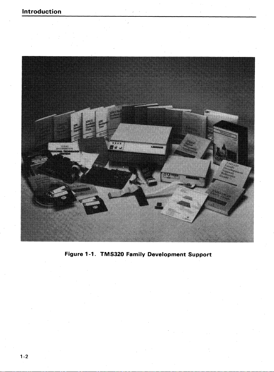
application reports. Figure 1-1 shows the wide range
available.
DSP applications
including hardware and software development products, product
with
an
extensive program
DSP design workshops, and a variety
of
development
of
development tools
1-1
Introduction
1-2
Figure
1-1.
TMS320
Family
Development
Support

Introduction
1.1
How
to
Use
This
Manual
The TMS320 Family Development Support Reference Guide details the vast
development support available for the TMS320 family
cessors.
ment making
necessary
that
Information concerning all aspects
it
an
tools for design and development
TMS320 refers
effective reference guide
to
both the first and second generations
is
consolidated into this docu-
to
assist the user in selecting the
of
of
digital signal pro-
TMS320 applications. Note
of
DSP
devices.
Sections 1 and 2 provide
ties for the user unfamiliar
for the first time. Sections 5, 6, and 7 describe the software and hardware
development products and Section 9 the extensive documentation available
to
support the wide range
Sections
each
assist in selecting which product(s}
and workshops that provide hands-on experience using the
tools.
Section
Section
Section
Section
Section
5,
6,
phase
Appendix A gives ordering information.
and 7 describe the development products available to support
of
DSP design. These sections also provide information that
2.
The TMS320 Digital Signal Processor Family. Description,
key features, and
List
3.
4.
5.
6.
ROM
the procedure for
Quality
quality
TMS320 Development Support Products. Discussion
TMS320 software and hardware development flow.
Software Support'
opment and the following products:
• TMS320 Macro Assembler/Linker
• TMS320 Simulator
, • SoftWare Development System (SWDS)
• Digital Filter
• Digital Signal Processing Software Library
• TMS320 Bell 212A Modem Software.
an
overview
with
of
applications using the TMS320 family.
of
possible applications.
Codes. Discussion
and Reliabilitv. Discussion
and reliability criteria for evaluating performance.
of
digital signal processing and investigating
the TMS320 family and its capabili-
to
use.
Section 8 describes the seminar
development
block diagram
implementation.
Products. Information on software devel-
Design Package (DFDP)
of
TMS320 family members.
of
ROM codes (mask options) and
of
Texas Instruments
can
of
it
Section
7.
Hardware Development Tools. Information on hardware de-
velopment and the following tools:
• TMS320 Evaluation Module
• TMS320 Emulator (XDS)
• TMS320 XDS
• TMS320 Analog Interface Board
• TMS320 DSP Design Kit.
Upgrade Program
(EVM)
(AlB)
1-3
Introduction
Section
Section
Section
Section
Appendix
Appendix
Appendix
8.
RTC
TMS320 Seminar
and
Workshops. Description
half-day technical seminar and three-day workshops
of
the
sponsored by the TI Regional Technology Centers (RTC). Address list
9. TMS320 Documentation Support. Discussion
of
the worldwide
RTCs.
of
TMS320
documentation available, including data sheets, user's
guides, application reports, textbooks, technical articles,
newsletters, bulletin board, and hotline.
10. TMS320 University Program. Information about the
TMS320 hardware
count
to
universities. List
professors on
TMS320 devices. Recommendations on establishing
workstations and
11. TMS320 Third-Party Support. Description
nufactured by other companies, which
development. Address list
and
software products offered at a dis-
of
DSP
theories and applications using the
research
textbooks written by university
stations in universities.
of
of
can
third parties. List
products ma-
assist
DSP
in
TMS320
of
lab
digital
signal processing consultants. '
A.
TMS320 Product Order Information. Device packaging ,information and product part numbers. Explanation of TMS320
device and development support prefixes and nomenclature.
B.
Texas
Outline
Instruments Factory Repair and Exchange Policy.
of
policies and procedures for repairing or exchang-
ing a damaged system.
C.
Texas
Instruments
Pr<jlgram
License Agreement.
1-4

2. The
TMS320
Digital Signal Processor Family
The TMS320 family
bines the
an
multichip bit-slice processors .
. The combination
data buses separated) and its
tion set provide speed and
capable
TMS320 family optimizes speed by implementing functions in hardware that
other processors
proach provides the design engineer
single chip.
The
The first generation contains the
TMS32010-25, TMS32011, TMS320C10, TMS320C10-25,
TMS320C15/E15, TMS320C15-25, TMS320C17 /E17,
The
Many features
TMS320 is used,
devices.) Some specific features
ferent cost/performance tradeoffs. Software compatibility is maintained
throughout the
processor
This section describes
key features, and provides functional block diagrams. Typical applications
also suggested.
some
major topics:
flexibility
array processor, offering
of
executing ten MIPS (million instructions per second). The
TMS320 family consists
TMS32020 and TMS320C25
has
fundamental DSP operations. Included in this section
of
16/32-bit
of
a high-speed controller
of
the TMS320's Harvard-type architecture (program and
flexibility to produce a MOS microprocessor family
implement through software. This hardware-intensive ap-
are
common among the TMS320 processors. (Note that when
it
refers
to
family
software and hardware tools
to
protect the user's investment in architecture.
each
Two
tables provide comparisons
single-chip digital signal processors com-
with
the numerical capability
an
inexpensive alternative to custom VLSI and
special digital signal processing (DSP) instruc-
with
power previously unavailable on a
of
two
generations
TMS3201 0 and its spinoffs: TMS3201 0-14,
are
the second-generation processors.
both the first and second generations
are
added in
member
of
the first and second generations, lists
of
digital signal processors.
and TMS320C17 -25.
each
processor
to
facilitate rapid design.
of
device performance for
are
to
provide
the following
of
DSP
Each
of
dif-
are
• First-Generation Devices (Section
• Second-Generation Devices (Section 2.2 on page
• Typical Applications (Section 2.3 on page
Figure 2-1 shows the generations
plotted
provides
of
on a hypothetical performance versus technology scale. Table 2-1
an
overview
memory, I/O, cycle timing, package type, technology, and military support.
of
the TMS320 family
2.1
on page
of
processors on a TMS320 family road map,
of
2-4)
2-9)
2-12)
processors
with
comparisons
2-1

The
:
P:
:
E:
:R:
: F:
,0:
:
R:
:M:
:A
:N:
c:
:
E:
TMS320
Digital
Signal Processor Family
<€:"
GENERA"§!>
1;g;;,H;;t;;;;;:;;;;;;;;"tt;;;";;;,,,,;;;;;(:
Figure 2-1. The
2-2
.~.O<:.;.~.~.~.
~~~~?:,iXiy.
TMS320
Family Roadmap
:
.tt?;;;;;;;;;;;;;;';;;;;;;;;";;;;;";;";;;;;;;;;;;·

The
TMS320
Digital
Signal
Table
Processor
2-1.
TMS320
Family
Family
Overview
DEVICE
TMS32010-14
(NMOS)
TMS32010t
(NMOS)
TMS32010-25
(NMOS)
TMS32011
(NMOS)
TMS320C10:l:
(CMOS)
TMS320C10-25
(CMOS)
TMS320C15
(CMOS)
TMS320C15-25
(CMOS)
TMS320E15
(CMOS)
TMS320C17
(CMOS)
TMS320C17
(CMOS)
TMS320E17
(CMOS)
TMS32020:l:
(NMOS)
TMS320C25:1:
(CMOS)
= serial;
'SER
··On-chip
tMilitary version available.
:l:Military versions planned; contact nearest
EPROM.
ON-CHIP
RAM
144 1.5K
144 1.5K
144 1.5K
144
144
144 1.5K
256
256 4K
256 4K"
256 4K
-25 256 4K
256 4K"
544
544
PAR
= parallel.
MEMORY
ROM
PROG
1.5K
1.5K
4K
4K
OFF-CHIP
4K
4K
4K
4K
4K
4K
4K
4K
64K
64K
DATA
sales
SER
2 6x16
2 6x16
2 6x16
2 6x16
64K
64K
1
1 16x16
office for availability.
I/O'
PAR
8x16
8x16
8x16
8x16
8x16
8x16
8x16
8x16
16x16
CYCLE
TIME
(ns)
280
200
160
200
200
160
200
160
200
200
160
200
200
100
PACKAGE
TYPE
DIP
PLCC PGA
40
40
40
40
40
40
40
40 44
40
40
40 44
40
44
44
44,
44
68
68 68
2-3

The
TMS320
2.1
First-Generation
The first generation
TMS32010-14, TMS32010-25,
2.4-lJm NMOS technology,
TMS320C15/E15, TMS320C15-25, TMS320C17/E17,
processed
member
The
of
memory
of off-chip program memory
a microcomputer version,
to 2.5K words
ROM-code version
prototyping, code update, and field upgradeability.
The
alternative
quency
well suited include servo control, high-speed controllers, low-end modems,
audio processing, data encryption, and vibration
ecute 3.5
in 280
cycle
system
compatible
ment tools.
The
TMS32010,
program memory
million instructions per second) than the TMS32010. Existing TMS32010
designs
the input
Family -First-Generation
Devices
Devices
of
the TMS320 family includes the TMS32010,
and
and
in
2.0-lJm CMOS technology. This section briefly desoribes
of
the first generation, lists key features,
TMS32010,
achieving a 16 x
of
TMS32010-14, a 14-MHz
of
million imstructions per second
ns.
program memory
development and modification. The device
TMS32010~25,
can
clock cycle time
the first TMS320 family member,
144 words
for
the TMS32010. Some applications for which the TMS32010-14
The TMS32010-14 provides a direct
with
is
take advantage
16-bit
of
off-chip program memory for a total
can
DSP
applications not requiring the maximum .operating fre-
the higher-frequency,
intended for higher-performance applications that
and
multiply in a single 200-ns cycle. On-chip data
is
available. Full-speed execution from up to 4K words
is
possible. The TMS32010
with
1.5K words
also operate entirely from off-chip ROM for
version
access,
a 160-ns instruction cycle time version
require 25 percent greater processor throughput (6.25
thereby offering a cost-effective method for
of
the enhanced throughput simply by increasing
to
25 MHz without rewriting software.
TMS32011, which
the TMS320C10, TMS320C10-25,
and
is
a microprocessor capable
of
program ROM on.-chip
of
the TMS3201 0, provides a low-cost
analysis. The device
and
perform a 16 x
EPROM
20-MHz
is
TMS32010 and its develop-
are
processed
and
TMS320C17-25,
provides block diagrams.
is
also available
of
4K words. This
16-bit
interface for single-
pin-for-pin
and
use
in
each
in
and
up
ease
of
can
ex-
multiply
software
of
the
off-chip
is
2-4
The
TMS320C10
pin-for-pin compatible
2.0-lJm CMOS technology, achieving a power dissipation
that
of
the
phony and portable consumer products. A
the
The
instruction cycle time. Its lower power
for high-performance
The
compatible with the TMS3201.0
words and on-chip program
of
TMS320C15
the NMOS device. Because
TMS320C1 0
TMS320C1
TMS320C10-25, a 25-MHz
TMS320C15
4K words. The devices
has
a 200-ns instruction cycle time and
with
the TMS3201
is
ideal for power-sensitive applications such
O.
The TMS320C1 0
of
its low-power dissipation (165 mW),
masked
O.
version of the TMS320C10,
and
DSP
applications. '
and
TMS320E15
is
also
available in a 160-ns version, the
and
ROM (TMS320C15)
are
processed
higher speed make
are
fully object-code and pin-for-pin
offer expanded on-chip RAM
in
2.0-lJm CMOS technology. The
ROM option
or,
EPROM (TMS320E15)
TMS320C15-25.
is
object-code
is
processed in
less
than one-sixth
as
digital tele.
is
available for
has
it
well suited
and
a 160-ns
of
256

The
TMS320
Family -First-Generation
Some
of
the key features
TMS320C10, TMS320C10-25, TMS320C15/E15,
of
Devices
the TMS32010, TMS3201 0-14, TMS32010-25,
and
TMS320C15-25
are:
• Instruction cycle timing:
• On-chip
• On-chip
•
•
• External memory expansion up
•
• On-chip clock generator
• Single 5-V supply
• Device packaging
• Technology:
160 ns (TMS3201 0-25, TMS320C1 0-25, TMS320C15-25)
200
ns
(TMS3201 0/C1
280
ns
(TMS32010-14)
data RAM:
144 words
256 words
program ROM:
1.5K words (optional)
4K words
4K words
16 x
16-bit
Barrel
shifter
40-pin DIP
44-lead
2.4-lJm NMOS: TMS32010, TMS32010-14, TMS32010-25
2.0-lJm CMOS: TMS320C1
(TMS320C15/E15, TMS320C15-25)
(TMS320C15, TMS320C15-25)
of
on-chip program
parallel multiplier
(see
Table
PLCC
0,
TMS320C15/E15)
EPROM
with
to
2-1):
(TMS320E15)
32-bit
result
4K words at full
0/C1 0-25,
speed
TMS320C15/E15/C15-25.
2-5

The
TMS320
Family - First-Generation Devices
+5
V GND
t t
INTERRUPT
144-WORD RAM
..
1.5K-WORD ROM
32-BIT ALUIACC
r
CJ
L
MULTIPLIER
SHIFTERS
DATA
~
ADDRESS
(16) •
(12).
.
Figure
INTERRUPT
----
Figure
2-2.
TMS32010,
......
-1
2-3.
TMS320C15/E15,
TMS32010·14,
TMS320C10-25
+5
V
256-WORD RAM
.4K-WORD
ROM/EPROM
. MULTIPLIER
32-BIT
ALU/ACC
SHIFTERS
TMS320C15-25
TMS32010~25,
Block Diagram
GND
DATA
ADDRESS (12)
Block Diagram
TMS320C10,
(16)
2-6

The
TMS320
Family -First-Generation
Devices
The TMS32011
program
applications. The device
includes a dual-channel serial interface, on-chip companding hardware
(1J-law/A-law), serial port timer, and a peripheral mode for prototyping.
The
words
dual-channel serial interface, on-chip companding hardware
and a serial port timer. The devices
TMS32010,
also available in a 160-ns version, the TMS320C17-25.
Many key features
tures
• Instruction cycle timing:
•
•
•
• Dual-channel
• Direct interface to combo-codec .
• Serial
• On-chip companding hardware for IJ-Iaw
• Object-code compatible
• Compatible with TMS3201 0 development support tools
• Peripheral
• Device packaging
• Technology:
ROM (and no external memory expansion) intended for high-volume
TMS320C17
of
on-chip program ROM (TMS320C17) or
of
the TMS32011, TMS320C17/E17,
On-chip data RAM:
On-chip program ROM:
4K words
(TMS32011 )
is
a dedicated microcomputer
is
object-code compatible with the TMS3201 0, and
and
TMS320E17
and
processed
are
160
ns
(TMS320C17-25)
200
ns
(TMS32011, TMS320C17/E17)
144 words
256 words (TMS320C17/E17, TMS320C17-25)
1.5K words (TMS32011)
4K words (TMS320C17, TMS32017-25)
of
on-chip program
serial port for fu"-duplex serial communication
port timer for standalone serial communications
mode to TMS32010 for application development
40-pin DIP
44-lead
2.4-lJm NMOS: TMS32011
2.0-lJm CMOS: TMS320C17
PLCC
in
2.0-lJm CMOS technology. The TMS320C17
common
(TMS32011)
with
(see
Table 2-1):
are
are
to
a" first-generation devices. Some key fea-
EPROM
the TMS3201 0 instruction set
IE17, TMS320C17 -25.
with
1.5K words
dedicated microcomputers
EPROM
object-code compatible
and
TMS320C17-25
(TMS320E17)
and
A-law PCM conversions
(TMS320E17), a
of
on-chip
with
4K
(1J-law/A-law),
with
the
are:
is
2-7

The
TMS320
Family - First-Generation Devices
+5
V
GND
DATA
(16)
INTERRUPT
r
CJ
INTERRUPT
DUAL-
CHANNEL
SERIAL
TMS32010
Figure 2-4. TMS32011 Block Diagram
+5
V
t
..
TMS320C15
OR
TMS320E15
PORT
p.-LAW/A-LAW
HARDWARE
TIMER
GND
t
DUAL-
CHANNEL
SERIAL
PORT
SERIAL
INTERFACE
ADDRESS
DATA
A.
SERIAL
INTERFACE
--
(3)
(16)
-"
2-8
r
CJ
L
Figure 2-5. TMS320C17/E17.
p.-LAW/A-LAW
HARDWARE
TIMER
TMS320C17-26
ADDRESS (3) "
Block Diagram

The
TMS320
Family - Second-Generation Devices
2.2 Second-Generation Devices
The second generation
cludes
two
of
these devices
TMS320
tures, and provides a
The
compatible
times the throughput
(109 instructions), large
set
spaces,
erful addition
Some key features
• 200-ns instruction cycle time
• 544 words
• 128K words
• Wait states for communication
•
• Single-cycle multiply/accumulate
• Repeat instructions
• Global data memory interface
• Block moves for data/program management
• Five auxiliary registers
• Serial port for multiprocessing or interfacing
• On-chip clock gE!nerator
• Single
•
members, the
family. This section briefly describes each device, lists its key fea-
TMS32020, processed in
with
on-chip
to
TMS32010
to-digital
2.4-l..Im
converters, etc.
5-V
NMOS technology,
of
the
is
the
serial port, and hardware timer make the
the
of
of
software compatibility
supply
TMS32020
based upon that
block diagram.
TMS32010
of
the first-generation devices. Its enhanced instruction
on-chip
TMS320
of
the
TMS32020
on-chip
total data and program memory space
data RAM
with
TMS320
family.
family
of
and the TMS320C25. The architecture
of
the TMS3201 0, the first member
2.4-l..Im
and in many applications
dedicated arithmetic
68-pin
NMOS technology,
data memory
are:
to
slower
instructions
grid array (PGA) package.
digital signal processors
(544
off-chip
is
source-code
is
capable
words), large memory
TMS32020 a pow-
memories
unit
to
codecs, serial analog-
of
of
in-
the
two
2-9

The
TMS320
Family -Second-Generation
The
TMS320C25
It
is
processed in 1.8-l.Im CMOS technology and
cycle time
creases
include 24 additional instructions, eight auxiliary registers,
hardware stack, 4K words
addressing mode,
cess.
pin-for-pin and object-code compatibility
Some
• 100-ns instruction cycle time
• 4K words
• 544 words
• 128K words
• Wait states for communication
• Object-code compatible
•
• Block moves for data/program management
• Single-cycle multiply/accumulate instructions
• Eight auxiliary registers
• Bit-reversed indexed-addressing mode for radix-2
• Double-buffered serial port
• On-chip clock generator
• Synchronization capability between multiple processors
• Single 5-V supply
• 1.8-l.Im CMOS technology: 68-pin grid array (PGA) package
of
the functionality
All
of
key features
24 additional instructions to support adaptive filtering,
tended-precision arithmetic
68-lead chip carrier (PLCC) package.
is
the newest member
100
ns.
The TMS320C25's enhanced feature
of
the device over the TMS32020. Enhancements
of
and
these improvements have
ofthe
of
on-chip program ROM (microcomputer version)
of
on-chip RAM
of
total program
on-chip program ROM, a bit-reversed indexed-
the low-power dissipation inherent
TMS320C25
with
with
Devices
of
the TMS320 second generation.
is
capable
been
achieved while maintaining
with
the TMS32020.
are:
and
data memory space
to
slower off-chip memories
the TMS32020
dedicated arithmetic unit
FFTs
of
an
instruction
set
greatly in-
an
eight-level
to
the CMOS pro-
FFTs,
and
ex-
and
2-10

The
TMS320
Family - Second-Generation Devices
+5
V GND
INTERRUPTS
D
INTERRUPTS
256-WORD I 288-WORD
DATA/PROGI
Figure
+5
RAM
MULTIPLIER
32-BIT ALU/ACC
SHIFTERS
2-6.
TMS32020
V
I
I
TIMER
DATA
RAM
T 1
256-WORD I 288-WORD
DATA/PROG
RAM
I
I
DATA
I
RAM
I
4K-WORDS ROM
DATA (16)
MULTIPROCESSOR
INTERFACE
SERIAL INTERFACE
ADDRESS (16)
Block Diagram
GND
DATA
..
.
MULTIPROCESSOR
INTERFACE
(16)
..
MULTIPLIER
32-BIT ALU/ACC
r
D SHIFTERS
L
Figure
2-7.
TIMER
TMS320C25
SERIAL INTERFACE
ADDRESS (16)
Block Diagram
2-11

The
2.3
TMS320
Typical
Family -Typical
Applications
Applications
The
TMS320 family's unique versatility
design approaches
can
simultaneously provide the multiple functions often required in those
in
a variety
of
complex applications. For example, a single TMS32020
hance the capabilities
speech
well
recognition, speech synthesis,
as
internal modem functions. Table
of
a professional computer by providing text-to-speech,
plications.
Table
2-2.
Typical
Applications
and
realtime performance offer flexible
applications.
and
DTMF encoding
2-2
of
the
TMS320
In
addition, TMS320 devices
can
be
used
and
decoding,
lists typical TMS320 family ap-
Family
to en-
as
GENERAL-PURPOSE DSP
Digital Filtering
Convolution Robot Vision Function Generation
Correlation Image Transmission/ Pattern Matching
Hilbert Transforms Compression
Fast
Fourier Transforms Pattern Recognition Transient Analysis
Adaptive Filtering Image Enhancement Digital Filtering
Windowing Homomorphic Processing
Waveform Generation
VOICE/SPEECH
Voice Mail Disk Control Secure Communications
Speech Vocoding Servo Control
Speech Recognition Robot Control Sonar Processing
Speaker Verification
Speech Enhancement Engine Control Navigation
Speech Synthesis
Text-to-Speech Radio Frequency Modems
TELECOMMUNICATIONS
Echo Cancellation FAX Engine Control
ADPCM Transcoders Cellular Telephones Vibration Analysis
Digital
PBXs
Line Repeaters Digital Speech Adaptive Ride Control
Channel Multiplexing Interpolation (DSI) Global Positioning
1200
to
Adaptive
DTMF Encoding/Decoding Spread Spectrum
Data Encryption
Radar
Power
Digital Audio/TV
Music Synthesizer Power Line Monitors Diagnostic Tools
Educational Toys Prosthetics
19200-bps Modems
Equalizers Video Conferencing
CONSUMER
Detectors Robotics Hearing Aids
Tools Numeric Control Patient Monitoring
GRAPHICS/IMAGING
3-
0 Rotation Spectrum Analysis
Workstations
Animation/Digital Map
CONTROL
Laser
Printer Control Image Processing
Motor Control
Speaker Phones Antiskid
X.25 Packet Switching Navigation
Communications
INDUSTRIAL
Security Access
INSTRUMENTATION
Seismic Processing
Phase-Locked Loops
MILITARY
Radar
Processing
Missile Guidance
AUTOMOTIVE
Brakes
Voice Commands
Radio
Digital
Cellular Telephones
MEDICAL
Ultrasound Equipment
Fetal Monitors
2-12
Table 2-3 provides a comparison
DSP
operations when using either a TMS32010, a TMS32020, or a
TMS320C25. Table
2-4
shows the benchmarks for the
providing cost-effective solutions to a wide range
of
performance for some
of
the fundamental
same
of
applications.
three devices
in
These

The
TMS320
Family - Typical Applications
performance figures can be further improved by additional optimization
algorithms for specific design
goals, such
as
CPU
loading and program space
requirements.
Table
2-3.
TMS320
FUNCTION TMS32010 TMS32020 TMS320C25 UNIT
Sample Time:
FI
R filter tap
Biquad II R filter tap 2 2 1
adaptive filter tap 1.4 1.2 0.4
LMS
(filter
and
update)
Sample
Rate:
256-tap
256-tap adaptive
Fast
64
256 complex-point:
1024 complex-point:
Matrix multiplication 5.4 5.4 2.7
[1 x 3]
FIR
straightline
straightline
[3 x 1]
filter:
I/O
FI
R filter:
I/O
I/O
I/O
Without companded
With companded
Without companded
With companded
Fourier Transforms:
complex-point 555 434 217
Radix-4
Radix-2 looped
Radix-4
Radix-2 looped 69.4 45 22.5
DSP Family Benchmarks
0.4 0.2
9.6 18.5 37 kHz
9.1
2.7 3.2 9.5
2.7
N/A
N/A
N/A
15.75
3.1
2.44 1.5
6.88 3.44
14.18
0.1
31.5
9.1
7.1
of
lis
lis
liS
kHz
kHz
kHz
liS
ms
ms
ms
ms
liS
the
Table
2-4.
TMS320
DSP System Benchmarks
PERFORMANCE
APPLICATION STANDARD TMS32010
Echo cancellation
(CCITI
G.165) (16
Data
encryption
(ANSI X3.92-1981 ) (42 kbps)
Split-band modem
(CCITI
V.22/212A) (full-duplex)
32-kbps ADPCM
(CCITI
G.721) (half-duplex)
2400-bps LPC-10
~O:l:
(DOD 45) (half-duplex)
16-kbps subband
coder
tRequires external program memory.
:l:Requires
external data memory.
Echo length
ms)
Data
rate
(full-duplex)
CPU
CPU
CPU
CPU
TMS32020t
N/A
100
loading
loading 100
loading
loading 80
TMS320C25
100 50
84 42
80
95
60 30
90 50
t:l:
:I:
70 3
75
2-13

2-14

3.
ROM
Codes
Board space
reduce chip count and provide the customer
Instruments offers microcomputer versions for many
members. The on-chip
customer's
al-purpose features
customizing the processor
To facilitate design, all prototype
microprocessor. (Note that TMS320 refers to both the first and second generations
test and refine algorithms for immediate results. When the algorithm
finalized, t!le customer
into the
MC/MP
The
TMS320 family members (excluding the TMS32011, TMS320C17/E17, and
TMS320C17-25), often shortens design and field upgrade cycle times,
thereby reducing expense. This mode permits the customer
as
a standard device operating
TMS320 code
processing
of
inventory obsolescence when the code is altered
An entire algorithm or
ROM space
ing external memory. With a reduced chip count and this program memory
flexibilty, multiple functions can
ware device, thus enhancing a product's capabilities.
is
often a critical concern in many
ROM
of
these processors
own
code. This allows the user to take advantage
of
TI's digital signal processors while at the
to
suit a specific application.
work
is performed using a standard TMS320
of
DSP
devices.) TMS320 development tools permit a designer
can
submit the code to
on-Chip ROM
(microcomputer/microprocessor) mode, offered on maskable
is
are
avoided. Field upgrade cycle times and the associated expense
of
a TMS320 DSP. TMS320 programs can also
of
the device.
out
of
altered during design, the delays associated
an
often-used routine may
be
more easily implemented in a single hard-
DSP
applications.
with
a single-chip solution, Texas
of
the TMS320 family
can
be
masked
Texas
Instruments to
to
use
external program memory. When
with
are
also avoided.
be
masked into the on-chip
be
In
order to
with
the
of
the gener-
same
time
to
has
been
be
masked
the TMS320
new silicon
expanded us-
The first-generation
TMS320C10,
TMS320C15 and TMS320C17
ond-generation
as
dered
ROM size
Figure 3-1 illustrates the procedure
parts. With any masked device order, there
mask tooling which includes 25 prototypes. A non-cancellable minimum
production order per year
TMS320C10, TMS320C15,
high-volume usage
The masked
a masked device. The customer's code must
of
the chosen processor.
TMS320C25
TMS320 DSPs
and TMS32011
TMS320C25
of
and TMS320C17. The TMS32011
with
a minimum production order per year
will
with
mask
with
1.5K words
with
4K words
with
4K words
flow
5000 units
be
available in 1987.
option include the TMS3201 0,
of
on-chip ROM, and the
of
on-chip ROM. The sec-
of
on-chip ROM
fit
for implementing TMS320 masked
is
a one-time charge
is
required for the TMS32010,
can
also
be
or-
within the specified
of
$5500 for
is
intended for
of
10,000 units.
3-1

ROM
Codes
CUSTOMER
CUSTOMER SUBMITS:
-
TMS320
- PRINT EVALUATION AND ACCEPTANCE FORM (PEAF)
- PURCHASE
-
TMS320
TEXAS INSTRUMENTS RESPONDS:
- CUSTOMER
-
CODE
NEW
CODE
ORDER
CODE
CODE
SENT BACK TO CUSTOMER
NO
TI PRODUCES
TMS320
RELEASE
FOR
MASK CHARGE/25 PROTOTYPES
INPUT INTO TI SYSTEM
25
DESIGN
FORM
FOR
VERIFICATION
PROTOTYPES
3-2
,Figure
NO
3-1.
TMS320
TMS320
PROOUCTION
ROM
Code
Flowchart

ROM
Codes
Leadtimes for the first 25 prototype units begin when the customer
mally verified that TI
production order begin once the customer
totypes. The typical leadtime for masked
for masked
TMS320
stantly strives
changes at any time.
has
recorded his code correctly. Leadtimes for the first
formally approves the masked pro-
production
to
improve these leadtimes and reserves the right
Please
10
to
12
contact the nearest TI Sales Office
TMS320
prototypes is 8 weeks and
weeks. Texas Instruments con-
leadtimes, further information on these procedures, and confirmation
to
for
has
for-
make
current
of
the
mask/production requirements.
TMS320
A
preferred media
PROM:
EPROM:
FLOPPY:
When a code
is
reformatted
verification
been reformatted,
user and
made involve deletion
and addition
ROM code may be submitted in one
is 5 1/4"
floppies):.
I
TBP28S166, TBP28S86
TMS2764,
TMS2508, TMS2516, TMS2532, TMS2564
TI Cross-Assembler Format
is
submitted
to
accommodate the TI mask generation system. System level
by
the customer
it
not
affect the execution
of
data in the reserved locations
to
Texas Instruments
is
is
important that the changes remain transparent
of
all address tags (unnecessary in a ROM code device)
therefore necessary. Although the code has
of
the algorithm. The formatting changes
of
the
following
for
a masked device, the code
of
the ROM for device ROM test.
formats (the
to
the
Note that because these changes have been made, a checksum comparison
not
a valid means
ROM code algorithms may also
a modem. Contact the nearest
of
verification.
be
submitted by secure electronic transfer via
TI sales office for further information.
With each masked device order, the customer must sign a disclaimer stating:
is
to
"The units
be shipped against this order were assembled, for ex-
pediency purposes, on a prototype (i.e., non-production qualified)
of
which
is
not
manufacturing line, the reliability
Therefore, the anticipated inherent reliability
fully characterized.
of
these prototype units
cannot be expressly defined."
and a release stating:
"Any
masked ROM device may be resymbolized
uct and resold
as
device at the convenience
ROM codes
will
be deleted from the TI system after one year from the last
though
it
were
an
of
Texas Instruments."
unprogrammed version
as
TI standard prod-
delivery.
of
the
3-3

3-4

4.
Quality
and
Reliability
The quality and reliability performance
Microcontroller Products,
and
signal processors, relies on feedback from:
• Our customers
• Our total manufacturing operation from front-end wafer fabrication
final shipping inspection
• Product quality and reliability monitoring.
Our customer's perception
judging performance. This concept
rate Quality Policy,
"For every product or service
ments that solve the customer's problems, and
those requirements
Quality and reliability programs at
and internal information
ability.
Texas
Instruments offers a leadership reliability qualification system, based
years
of
research into customer requirements. This system provides more than
liable products; feedback
continuing improvements in TI products. Data generated by the system
ways available
last input received
formance is the most important quality and reliability measurement.
experience
which
without
with
to
aid customers in qualifying TI products. Although
for
any product delivery cycle, customer-perceived per-
which
of
quality must be the governing criterion
is
as
follows:
exception."
to
achieve constant improvement in quality and reli-
leading-edge memory technology
of
results
of
Texas Instruments Microprocessor
includes the
is
the basis
we
offer,
TI
are
therefore based on customer
to
manufacturing and design leads
TMS320
for
Texas Instruments Corpo-
we
shall define the require-
we
shall conform
as
family
well
as
of
years
just
it
digital
to
input
is
is the
to
for
on
of
re-
to
al-
4-1

Quality
4.1
and
Reliability
Reliability Stress Tests
Accelerated stress tests
process changes
vironments used
• High-temperature operating life
Storage life
•
•
Temperature cycling
Biased humidity
•
• Autoclave
• Electrostatic discharge
• Package integrity
• Elec::tromigration
• Channel-hot electrons
Typical events or changes that require internal requalification
clude:
•
New die design, shrink, or layout
•
Wafer process (baseline/control systems, flow,
dopants, passivation, or metal systems)
• Packaging assembly (baseline control systems or critical assembly
equipment)
• Piece parts (such
wire, or
Manufacturing site.
•
TI
r~liability
controls
duct
serve
sites; enhancing
than
built-in product excellence.
and management include product ramp monitor
release
as
the leading indicator in wafer-process integrity at TI MOS fabrication
200,000 MOS devices per month on reliability test
to
lead finish)
control systems extend beyond qualification. Total reliability
controls. MOS memories, utilizing high-density active elements,
all MOS logic device yields and reliability.
are
to
ensure product reliability excellence. The typical test en-
qualify new products or major changes in processing
performed on new semiconductor products and
(performed on geometries
as
lead frame, mold compound, mount material, bond
less
than 2.0
of
mask,
chemicals,
as
well
as
TI
to
ensure and sustain
11m).
product
final pro-
places more
are:
in-
gases,
4-2
Table
4-1 lists the microprocessor and microcontroller reliability tests, the du-
ration
of
the test, and sample
tests in the
table.
AOQ (Average Outgoing Quality) Amount
. ulation, usually expressed in terms of
FIT (Failure In Time)
Operating
lifetest
size.
The following defines and describes those
I
parts per million (PPM).
Estimated field failure rate in number
of
hours;
fail per
Device
ambient temperature
to
of
defective product in a pop-
failures per billion power-on device
1000
FITS
1000 device hours.
dynamically exercised at a high
simulate field usuage that would
equals
(usually 125°C)
0.1
percent

Quality
and
Reliability
expose the device to a much lower
ambient temperature (such
Using a derived high temperature, a
55·C ambient failure rate
culated.
can
as
be cal-
55·C).
High-temperature
Biased
Autoclave
Temperature
humidity
(pressure
cycle
storage
cooker)
Device exposed to
condition. Bond integrity
this environment.
Moisture and bias used
corrosion-type failures
packages.
ambient temperature
relative humidity (RH). Typical bias
voltage
nating pins.
Plastic-packaged devices exposed to
moisture at
one atmosphere above normal pressure. The pressure forces moisture
permeation
erates corrosion mechanisms
ent) on the device. External package
contaminates can also be activated
and caused
rent leakage paths.
Device exposed
extremes in
(-65·C
15
minutes per cycle) for at least
cycles. Package strength, bond quality, and consistency
cess
Conditions include 85·C
is
+5
121·C using a pressure
of
to
an
for
15
are
stressed in this environment.
150·C unbiased
is
stressed in
to
accelerate
in
plastic
with
85-percent
V and ground on alter-
the package and accel-
generate
to
severe temperature
alternating fashion
minutes and 150·C for
of
(if
pres-
inter~pin
assembly pro-
cur-
1000
of
Thermal
PIND
Mechanical
shock
Sequence:
Fine and gross leak
Mechanical shock
PI
N D (optional)
Vibration, variable frequency
Constant acceleration
Fine and gross leak
Test similar
test, but involving a liquid-to-liquid
transfer, per
1011.
Particle Impact Noise Detection test.
A non-destructive test.to detect loose
particles inside a device cavity.
Per
M I L-STD-883C, Method 1014.5
Per
MIL-STD-883C, Method 2002.3,
1500
Per
MIL-STD-883C, Method 2020.4
Per
MIL-STD-883C, Method 2007.1,
20 g, Condition
Per MIL-STD-883C, Method 2001.2,
20
kg, Condition
Per
MIL-STD-883C, Method 1014.5
g,
to
the temperature cycle
MIL-STD-883C, Method
0.5
ms,
Condition B
A .
D,
Y1
Plane min
4-3

Quality and Reiiability
Electrical test
Thermal Sequence:
Fine and gross leak
Solder heat (optional)
Temperature cycle
(10 cycles minimum)
Thermal shock
cycles minimum)
(10
Moisture
Fine and gross
Electrical test
resistance
leak
Thermal/Mechanical Sequence:
Fine
and
gross leak
Temperature cycle
(10 cycles minimum)
Constant acceleration
Fine and gross leak
Electrical test
Electrostatic discharge
Solderability
Solder heat
Salt atmosphere
Lead
pull
Lead
integrity
Electromigration
Resistance to solvents
To data
Per
Per
Per
-65
Per
-55
Per
Per
To data sheet limits
Per
Per
-65 to +150·C, Condition C
Per
30 kg,
Per
To data sheet limits
Per
Per
Per
10sec
Per
Condition
Per
Condition A
Per
Condition
Accelerated stress testing
ductor patterns
lifetime
Per
sheet limits
MIL-STD-883C, Method 1014.5
MIL-STD-750C, Method i 014.5
MIL-STD-883C, Method 1010.5,
to
+150·C, Condition C
MIL-STD-883C, Method 1011.4,
to
+125·C, Condition B
MIL-STD-883C, Method 1004.4
MIL-STD-883C, Method 1014.5
MIL-STD-883C, Method 1014.5
MIL-STD-883C, Method 1010.5,
MIL-STD-883C, Method 20()1.2,
Y1
Plane
MIL-STD-883C, Method 1014.5 .
MIL-STD-883C, Method 3015
MIL-STO-883C, Method 2003.3
MIL-STD-750C, Method 2031,
MIL-STD-883C, Method 1009.4,
A,
24,
hrs
min
MIL-STD-883C, Method 2004.4,
MIL-STD-883C, Method 2004.4,
B1
of
to
ensure acc,eptable
of
power-on operation
MIL-STD-883C, Method 2015.4
con-
4-4

Quality
and
Reliability
Table
4-1.
Microprocessor
and
MicrocontrollerTests
TEST
Operating life, 125·C, 5.0 V 1000 hrs 195
Op~rating
Storage life, 1 50·C
Biased
Autoclave,
Temperature cycle, -65
Thermal shock,
Electrostatic discharge,
Latch-up
Mechanical sequence
Thermal sequence
Thermal/mechanical sequence
PIND
Internal water vapor
Solderability 22 22
Solder heat 22 22
Resistance
Lead
Lead
Lead
Salt atmosphere
Flammability
Thermal impedance 5 5
·If
TI
Qualification test updates
life, 150·C, 5.0 V
85·C/85 percent
121
·C, 1 ATM
-65
(CMOS devices only)
to
integrity 15 15
pull
finish adhesion
junction temperature does not
solvents 12 12
(UL94-VO) 3
RH,
5.0 V 1000 hrs 129
to
150·C 1000 cyc
to
150·C 500 cyc 129 129
± 2
kV
exceed
are
available upon request at no charge.
consider performing any additional reliability test(s),
TI
information on
sales
office.
quality and reliability programs, contact the nearest n field
DURATION
1000 hrs
1000
240
plasticity
hrs
hrs
of
package.
SAMPLE
PLASTIC
SIZE
CERAMIC
77·
129 129
105
129 129
12 12
5 5
-
-
-
-
-
15
15
15 15
if
requested. For more
195
77
-
-
38
38
38
15
5
-
15
-
TI
will
Note:
Texas
Instruments reserves the right
ductor test
limits, procedures, or processing
arrangements for notification have
to
make changes in MOS Semicon-
been
without
made, TI advises all customers
notice. Unless prior
reverify current test and manufacturing conditions prior
published data.
to
relying on
to
4-5

4-6

5.
TMS320
Development
Texas
Instruments offers
to assist the user in
products range from development and
ware development and integration systems such
Support
an
extensive line
a"
aspects
Products
of
of
TMS320 design and development. These
application software to complete hard-
development support products
as
the XDS/22.
System
(EVM) or Emulator
the processor's performance, benchmark time-critical code, and determine the
feasibility
tensive documentation provides information concerning device specifications
and capabilities. The
DSP design workshops that provide hands-on experience
velopment
Software and hardware can
assembler/linker and simulator for software development and the
hardware development. The
source program into
XDS, or
erful tool for debugging and integrating software and hardware modules.
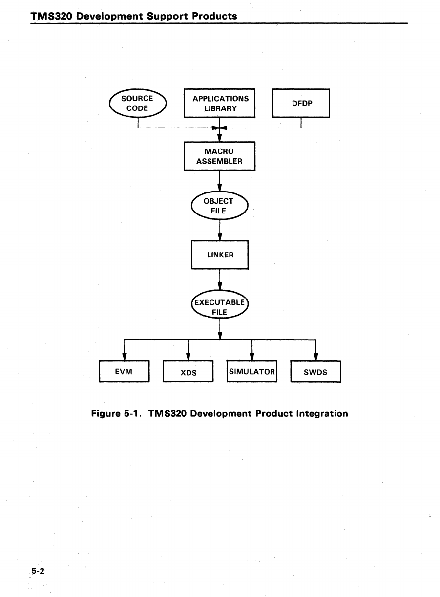
Figure 5-1 shows development product integration, and Figure
typical application development. The appropriate
is indicated for
of
ment purpose, software and hardware features,
development begins
(XDS). These support tools allow the designer
of
using a TMS320 device to implement a specific algorithm.
tools (see Section 8.2).
an
EVM.
The XDS provides realtime in-circuit emulation
each
stage
the TMS320 development tools, comparing capabilities such
with
the
use
of
the TMS320 Evaluation Module
to
evaluate
TI
Regional Technology Centers (RTCs) offer three-day
with
TMS320 de-
be
developed in para"el by using the macro
XDS for
assembler/linker translates the system's assembly
object module that can
of
development. Table 5-1 provides a feature matrix
be
executed by the simulator,
and
is a pow-
5-2
TMS320 support product
as
develop-
and
amount
of
memory.
Ex-
shows
5-1
TM$320
Development Support Products
APPLICATIONS
LIBRARY
MACRO
ASSEMBLER
LINKER
DFDP
Figure 5-1.
TMS320
Development Product Integration

TMS320
Development
Support
Products
CONCEPTUAL
STAGE
TMS320
EVALUATION
HARDWARE/
SOFTWARE
DESIGN
HARDWARE/
SOFTWARE
INTEGRATION
HARDWARE
XDS
DSP APPLICATIONS
ASSEMBLER/LINKER
DESIGN
SYSTEM DEBUG
XDS
SOFTWARE DESIGN
ASSEMBLER/LINKER,
SIMULATOR
SWDS
(TMS32020/C25)
Figure 5-2. Typical
TMS320
Application
Development
Flow
5-3

TMS320
Development
Support
Products
Table 5-1. Feature
FEATURES
Development Purpose:
Evaluation/benchmarking
Software development
Hardware design No
Line-by-line assembler/reverse assembler
Modify/display memory and registers
Single-stepping
Breakpoint on address
Breakpoint on memory access/read/write No
Time-stamping/clock counter No
Real-time trace samples No No No
Full-speed in-circuit emulation:
From on-board memory
From target memory
Multi-user system No
Built-in
Files associated
Amount
system interface No No
to
I/O
ports
of
On-board program/data
memory:
On-board program/data (TMS32020/C25)
Program/data expansion (TMS320C25) 6K/16K
" Memory expansion board allows
program and data memory. configurable in 1 K blocks.
(TMS3201 0/C1 0)
Matrix
for
of
TMS320
EVM
Yes
No
Yes
Yes
Yes Yes Yes
Yes
Yes
No
No
4K/-
4K/4K
memory expansion
Development Tools
SIMULATOR SWDS
Yes Yes
Yes
No No
No
Yes
Yes
Yes
Yes
N/A
N/A
Yes
Yes
N/A
N/A
N/A
to
64K words total
.
Yes
Yes
Yes.
Yes
No
Yes
Yes
No
No
Yes
Yes
N/A
N/A
24K
XDS
Yes
Yes
Yes
Yes
Yes
Yes
Yes
Yes
Yes
Yes
Yes
Yes
No
No
No
4K/-
4K/4K
64K"
of
5-4

6.
Software
Support
Products
Many support products
processors. This section discusses the software support products, which include a macro assembler/linker, simulator, SoftWare Development System
(SWDS), Digital
TMS320 Bell
sections listed
• TMS320
• TMS320 Simulator (Section 6.2 on page
• SoftWare Development System (SWDS) (Section 6.3 on page
• Digital Filter Design Package (DFDP) (Section 6.4 on page 6-10)
• Digital Signal
• TMS320 Bell 212A Modem Software (Section 6.6 on page
Filter Design Package (DFDP), DSP Software Library, and
212A
below.
Macro Assembler/Linker (Section
are
offered for the TMS320 family of digital signal
Modem Software. These products
6.1
6-5)
Processing Software Library (Section 6.5 on page
are
on page
described in the
6-2)
6-15)
6-7)
6-13)
6-1

Software
6.1
TMS320
Development Tools -
Macro
Assembler/Linker
Macro
Assembler/Linker
The TMS32o. Macro Assembler
TMS32o. assembly language instructions and directives into executable object
code. The assembler
hexadecimal machine instructions and
symbolic
code. When'several components
ually, the TMS32o. Link Editor links together the object code produced by the
program modules to form one complete executable program.
The
Assembler/Linker:
• Macro capabilities
• Macro definition library
• Macro-conditional assembly
• Relocatable modules
• Complete error diagnostics
• Symbol and cross-reference tables.
The
(160.0.
erating
In the assembler, directives control the assembly process rather than produce
object code. The assembler supports directives that
and the assembler output, initialize constants, and resolve external references.
The assembler
this file may contain either
comment. The assembler produces
that shows the source statement number, a location counter value, the object
code assembled, and the source
that contains the actual object code that
The assembler also provides a complete set of error messages and
symbol table and cross-reference listing.
addresses.
following versatile features distinguish the TMS32o. Macro
TMS32o. Macro Assembler/Linker is currently available for the VAX/VMS
BPI mag tape) and
sys~ems.
uses
allows the programmer
A source file
The
TI/IBM
PC
configuration requires a minimum
TMS32o. source code
an
is
a two-pass assembler that translates
to
use
to
can
of
a source program
PC
assembler directive, a machine instruction, or a
two
stateme"nt
reference memory locations
contain either absolute or relocatable
MS/PC-DOS (5
as
input.
output files: (1) a source listing file
as
entered; and (2)
can
mnemonics rather than
are
assembled individ-
1/4-inch
affect the location counter
Each
source statement in
be
executed by the TMS32o..
floppy) op-
of
256K RAM.
an
an
object file
with
optional
6-2
The assembler supports macro
tional assembly
source code. Macros may
library (directory)
The
TMS32o. Link Editor permits modular programming; a program
designed
sembled and then linked
editor's major function
nitions.
name, defines the starting location for the data and program segments, and
indicates
output files: (1) a listing
the segments and modules, which were linked, and a cross-reference listing
of
module
As
the externally defined variables; and (2) a file that contains the actual load
of
to
simplify programming and consolidate frequently repeated
of
external files
and
implemented in separate modules that
input, the link editor
which object files
linked object code, which can
is
calls and definitions
be
defined
to
form a complete executable program. The link
to
resolve external symbolic references and defi-
are
of
the command control file that includes a map
with
to
uses
to
be
the assembler source code or in a
be
included at link time.
a link control file that specifies the task
linked. The link editor produces
be
executed by the TMS32o..
as
well
can
as
macro-condi-
be
individually
can
be
as-
two
of

Software
Development
Tools -Macro
Assembler/Linker
TMS320 source code
and then downloaded
module,
or XDS emulator. Figure 6-1 shows
can
be
written in a single source file, assembled, linked,
to
the TMS320 program memory, simulator, evaluation
module.
SOURCE
MODULE
Figure
A TMS320 program
Figure
6-2
link control file, and then downloaded
shows
6-1.
Assembly
can
how
these modules
also
with
be
separated into
are
to
a Single..;Source
the TMS320 program memory, sim-
ulator, evaluation module, or XDS emulator.
an
.assembly
LISTING
FILE
with
a single-source
TMS320
PROG. MEMORY
SIMULATOR
EVM
XDS
Module
two
or more source modules.
assembled individually, linked via a
6-3

Software
SOURCE
MODULE
SOURCE
MODULE
Development Tools -
CONTROL
Macro
LISTING
FILE
OBJECT
CODE.
LINK
FILE
OBJECT
CODE
LISTING
FILE
Assembler/Linker
TMS320
PROG. MEMORY
SIMULATOR
EVM
XDS
MAP
LISTING
6-4
Figure 6-2. Linked Assembly
The
latest revision number
of
referenced through the TMS320
9.8).
with
Multiple-Source
Modules
the TMS320 assembler/linker software
DSP
Bulletin Board 'Service
(see
can
be
Section

Software
6.2
TMS320
Development
Simulator
Tools -
Simulator
The TMS320 Simulator
croprocessor and microcomputer modes for cost-effective
development and program verification in nonrealtiine. Using the inexpensive
software simulator
Files may be associated
during test and debug. Time-critical code
portions
optimization. Breakpoints can be established, based on
cution
Significant key features
• Interrupt generation at user-defined intervals
• File-associated
• Programmable breakpoints on:
• Timing analysis relative
• Trace on accumulator, program counter, and auxiliary registers
• Immediate execution
• Data and program memory modification and display:
• Error
• Command execution from a journal file
• Modification and inspection
• Multiple-user configuration
of
the program. The clock counter allows loop timing during code
with
internal data RAM.
(TMS32020/C25)
Instruction acquisition
Memory reads or writes (data or program)
Data patterns on the
Error conditions.
Changing
Initializing memory before a program
messages
is
a software program that simulates the TMS320 mi-
TMS320 software
allows debugging.
with
I/O
of
the simulator
I/O
with
to
of
an
an
entire block at any time
for illeg,al opcodes and invalid data entry
without
ports so that specific
are:
8 ports (TMS32010) or
D-busor
clock rate
interrupt or instruction
of
registers
(VAXNMS
the requirement
can
be
tested,
the P-bus
is
loaded.
system).
I/O
values may
as
well
read
of
hardware.
be
used
as
individual
and write exe-
16
ports
The
TMS320 Simulator
mag tape) and
The
PC
Simulator
The simulator
Assembler/Linker. Input and output files may be associated
addresses
processor. The interrupt flag can
to
simulate
points and traces may be defined and enabled. Figure
of
a simulator screen display.
TI/IBM
configuration requires a minimum
and 512K RAM for the TMS32020/C25 Simulator.
uses
of
the
I/O
an
interrupt signal. Before initiating program execution, break-
is
currently available for the
MS/PC-DOS
TMS320 object code produced by the TMS320
instructions, simulating
(5
1/4-inch
of
256K RAM for the TMS32010
I/O
be
set periodically at programmed intervals
VAXNMS
floppy) operating systems.
devices connected to the
6-3
shows
(1600 BPI
with
the port
an
example
Macro-
6-5

Software
Development Tools -
Simulator
6-6
Figure 6-3. Simulator Screen Example
During program execution, the internal registers and memory
TMS320
cution is suspended when a breakpoint or error
'self'
Once program execution
and data memories can
also
journal file
during another
Before beginning a debugging session,
written and assembled.
linked. The linked absolute object code
cuted during simulation.
are
modified
is
detected, or a breakpoint from the keyboard is entered by the
be
displayed. A record
so
that
simulation session.
as
the host computer interprets
is
suspended, the internal registers and both program
be
inspected and/or modified. The trace memory
of
it
may
the simulation session can
be
re-executed
If
there
.are
to
TMS320 source code must first
multiple modules, then they must
is
loaded into the simulator and exe-
regain the
each
is
encountered, a branch
same
be
of
the simulated
instruction.
user.
maintained in a
machine state
Exe-
to
can
be
be

Software
6.3
SoftWare
Development
Development
Tools -SoftWare
System
Development
(SWDS)
System
The SoftWare Development System (SWDS), shown in Figure 6-4,
resident
and TMS320C25. The SWDS offers a user the system interface necessary to
write,
workstation. The debug capabilities
through the code
memory contents during execution.
I/O
ure
A circuit board, resident in the
and program and data memory.
outside the
The cable adaptor boards included
Connector that connects the
system via a 68-pin grid array footprint, and (2) the
(AlB)
AlB.
Library (see Section 6.5)
The
TI Business Pro),
MS-DOS version 2.0 or later is required.
The
with
to execute at full speed.
The
TMS320C25 and a
20-MHz
emulation.
the upper limit on the clock speed
on the
source, the external clock
mand and
tool that provides software simulation in realtime for the TMS32020
assemble/link, load, and debug the
of
or
to set software breakpoints for monitoring register or
It
ports so that specific
6-5
provides
Adaptor Connector that connects the SWDS directly
The
SWDS
development system occupies 64K bytes
24K words (48 kbytes)
SWDS is configured
crystal
PC
an
PC
and connect to the SWDS via
TMS32020/C25
is
designed to function in any
as
are
The target system may supply a
board.
an
external crystal
I/O
values may be used during test and debug. Fig-
example
well
40-MHz
included
If
of
a SWDS screen display.
PC,
contains the TMS32020 or TMS320C25
Two
with
SWDS to a TMS32020 or TMS320C25 target
assembler/linker software and the
are
included in the SWDS package.
as
in the
IBM-PC/AT
of
static RAM, and allows the TMS32020/C25
to
emulate the TMS320C25 upon shipment; i.e., a
oscillator
with
the system
is
the user's target system
is
specified in the debug monitor initialization com-
is
connected to the SWDS.
TMS32020/C25
the SWDS allow the user to single-step
is
also possible to associate files
small cable adaptor boards
two
40-conductor ribbon cables.
the system
TI
are
dictated by the speed
are:
(1)
the PGA Adaptor
Analog Interface Board
to
PC
environment (including the
and compatible environment.
of
PC
memory.
on-board. A TMS32020 and a
to
accommodate TMS32020
TIL
clock source, in which
of
has
no provision for a clock
is
a PC-
code on a
are
the TMS3201 0
DSP
It
is
the processor
PC
with
situated
Software
equipped
case
Texas Instruments constantly strives
right to make changes at any time in the specifications
velopment System.
to
improve its products, reserving the
of
this SoftWare De-
6-7

Software
Development
Tools -SoftWare
Development
System
6-8
Figure
6-4.
SoftWare
Development
System
(SWDS)

Software
Development
Tools -SoftWare
Development
System
Figure
6-S.
SWDS
Screen
Example
6-9

Software
6.4
Digital
Development
Filter
The Digital Filter Design Package (DFDP) from Atlanta Signal Processors, Inc.
(ASPI)
design
in a variety
is
of
Tools -Digital
Design
a user-friendly, menu-driven software package intended
digital filters
of
Package
with
filter structures.
Filter
Design
Package
(DFDP)
floating-point accuracy or
fixed-point
to
speed
economy
6-10
Figure
6-6.
Digital
Filter
Design
Package
(DFDP)

Software
Development Tools ~ Digital
Filter
Design Package
The package consists
forming the
1}
2}
3}
4}
Cascade and parallel structures
ized lattice, and orthogonal forms
The DFDP can design filters
tion, evaluate filter characteristics before and after coefficient quantization,
and design special-purpose
tors, Hilbert transformers, and raised-cosine filters. The DFDP
erate coefficients for filter implementations on any general-purpose processor
or signal processing chip,
for a variety
can be plotted for printer or screen display (see Figure
phase, group delay, and pole-zero map can be plotted for
The DFDP design modules present menus and queries so that the designer
can specify the type
and attenuation requirements. The program estimates the required filter order
or impulse response length and
used. The program then attempts
coefficients,
screen message may warn that specifications
signed filter does
If
the designed filter does
table
by the program
examine the response over the
sampling frequency) or over any narrower frequency limits chosen. Amplitude
is
automatically scaled
height
expansion
directed
After the filter is designed, the user can generate code associated
using the
following
Designing FIR filters (Kaiser
Designing FIR filters (Parks-McClellan)
Designing IIR filters (Butterworth, Chebychev I and II, and elliptic)
Generating TMS320 assembly code by converting the ASCII file containing the filter coefficients into
code for the
of
DSP chips. Magnitude, log magnitude, and impulse responses
it
calculates the response characteristics
of
poles and zeros or impulse response coefficients
of
the graph.
of
a narrower band, is displayed on the monitor and may also
to
the printer.
CGEN
of
four interactive filter design modules capable
functions:
window)
TMS3201 0 and TMS32020.
as
to
meet any piecewise linear response specifica-
FIR filters, such
as
well
of
filter, sampling frequency, and filter
asks
not
meet specifications.
not
meet specifications, the user may examine the
as
well
as'
the frequency response plots. The user may also
full relevant spectrum (zero to one-half the
within
Every
design module.
such a frequency band in order
plot, whether
fully commented assembly language
well
as
are
as
higher-performance lattice, normal-
included in the modules.
fully commented assembly language code
the user to select the filter length
to
calculate the coefficients; using these
of
of
per-
as
multiband filters, differentia-
6-7);
of
are
the full relevant spectrum or the
the realizable filter. A
unrealizable
of
can
also gen-
in addition, the
IIR filters.
cutoff
frequencies
to
or
that the de-
the filter generated
to
utilize the full'
with
the filter
be
be
The DFDP runs on the
erating systems must have
mation, contact Atlanta
nearest TI field sales office.
TI
PC,
IBM
192
Signal Processors, Inc. (see Section 11) or the
PC/XT/AT, and compatible systems. Op-
kbytes
of
memory available. For more infor-
6-11

Software
Development
Tools -
Digital
Filter
Design Package
tt
'
o
•.
.1
...
,
~
w
'"'
o
1·2
0·2
'\OdlO
MAGNITUDE
i
I
.. , .....
I
.,
I·!·;
I r I 1 1
f.
1
I
L_
'r:-:-:-=~~~'::;:-:-:-1-
1 1 • 1 t
I I , t
).,
:.
1
lit
r.
.!...!
t I I t
.1
•. 1 ..
1.
,.
/ I i I
I·
1 1 1
:i:
1.~El@@
LOG
7.00~0
FREQUENCY
MAGNITUDE
RESPONSE
....
.
...
3.0000
IN
KILOHERTZ'
RESPONSE
j
,.
·!·\l
j
•••
:
4.0000
.......
r·
.L
..
J····
1 ...... , ..
,:
.
5.0000
6-12
-80.08
-160.00
-0i.1Oi
-0.310
1.0000
UNIT
1.~800
Figure
7.0000
FREQUENCY
SAMPLE
3.1800
TIME
6-7.
DFDP
3.0000
IN
KILOHERTZ
RESPONSE
IN
4.7400
MILISECONDS
Plot Examples
<:~
5.0000
8.3200
7.9000

Software
6.5
Digital
Development
Signal
The Digital Signal Processing Software Library contains the major DSP routines (FFT,
algorithms
sented in the book, Digital Signal Processing Applications
Family. These routines and algorithms
TMS32020 source code. In addition, macros for the TMS3201 0
in the
library.
Tools
Processing
FIR/IIR filtering, and floating-point operations) and application
(echo cancellation, ADPCM, and DTMF coding/decoding) pre-
- DSP
Software
Software
are
Library
Library
with
the TMS320
written in either TMS3201 0
are
and/or
included
The software package consists
MS/PCVAXNMS
the contents
magnetic tape for the
file briefly describing the contents
to
TMS320 Family,
provides printed code in the appendices
indicates the section in the applications book where the user
theory behind the source code.
The software library and applications book
TMS320 Design Kit (see Section 7.5). The library can also be ordered separately.through TI (see Appendix A for ordering information).
All the software in the library
pendix C for the Program License Agreement). The library
updated; therefore, check the
for update information.
DOS (version
version. For the MS/PC-DOS version, Table 6-1 briefly describes
of
each diskette. All the directories listed
the code. The book,
1.1
VMS version.
is
the major reference for the theory and algorithms, and also
of
four diskettes for use
or later)
Digital
TMS320 DSP Bulletin Board (see Section 9.8)
or a 1600
Each
of
the files in the directory and the reference
Signal Processing Applications
of
is
copyrighted by Texas Instruments (see
BPI magnetic tape
directory contains a README.LlS
each application report. Table 6-1
are
included in the purchase
with
the
are
contained on the
can
is
continually being
TI/IBM
for
with
find the
the
the
of
Ap-
a
6-13

Software
Development
Tools
- DSP
Software
Library
Table
DISK
#
1 README.LIS 1
2
3
4
tTotal: 4 disks, 18 directories,
DIRECTORY
I NSTALL. BAT
LOAD. BAT 1 Loading
FFT32010.DIR 10
FFT32020.DIR 10
ADPCMCCI.DIR 9
ADPCMNON.DIR
COMPND10.DIR
COMPND20.DIR 4 Companding routines in TMS302020
COMPNDHW.DIR 3
DTMF10.DIR 4 Single-channel DTMF code in TMS3201 0 19
ECH0128.DIR 2 16-ms echo cancellation code in 15
FIR-IIR.DIR
GRAPHICS.DIR 20
FLTGPT10.DIR
FLTGPT20.DIR 4 Floating-point routines in TMS32020 7
MACROS.DIR 60 TM;;3201 0 Macros
MATRIX.DIR
ADPTVFLT.DIR
DATAIO.DIR
MACROSRC.DIR 37 More TMS3201 0 macros
6-1.
Software
#OF
FILES
Description
S/W
1
5
5
7
3
3
2
2 Conversion routines from TMS320/ .
191
files.
installation procedures
FFT
routines in TMS32010 (source)
code (from Burrus and
and
Convolution Algorithms)
FFT
routines in TMS32020 (source)
code
CCITI-compatible ADPCM code in
TMS32010
Non-CCITI
Companding routines in
FORTRAN programs
companding
companding in hardware
TMS32020
FI
Rill
R filter code in TMS32010/20 3
Graphics routines in TMS32020
Floating-point routines in TMS32010 6
Matrix
multiplication routines
TMS32010/20
in
Adaptive filter routine in
9900/7000 code into binary format
Library
DESCRIPTION
of
product
S/W
onto hard disk
ADPCM code in TMS32010 17
tables for implementing
Contents
Parks'DFT/FFT
TMS32010
to
generate 14
TMS32020
BK.
APP.
SECTION
4
17
5
5
23
9
6-14

Software
6.6
TMS320
Development Tools -
Bell 212A
Texas Instruments
documentation for the design and
modem
crocontroller.
The documentation included in the package consists
port discusses in
as
gorithms, and coding techniques used in the implementation
modem demonstration unit. This implementation has
verify its operation. After reading this report, the user should be able
and
making custom modifications.
The source code for the
provided on a 5
tems. Contact the nearest
with
the TMS32011 digital signal processor and the TMS7041
the functions implemented. The second report describes the hardware, al-
build a similar
1/4"
TMS320
Modem
is
offering a software package containing source code and
detail the theory behind the design
unit
as
TMS320 Bell 212A Modem Software package
floppy for
TI field sales office for further information.
Bell 212A
Software
implementation
well
as
understand some tradeoffs involved in
MS/PC-DOS
Modem
or compatible operating sys-
Software
of
a 1200-bps Bell
of
two
reports. One re-
of
the modem,
been
of
built
a Bell
and tested
as
to
212A
mi-
well
212A
to
design
is
6-15

6-16

7.
Hardware
Development
Tools
The hardware development support tools for the
signal processors include the Evaluation Module (EVM), Emulator
tended Development
DSP Design Kit. These tools
• TMS320 Evaluation Module (EVM) (Section
• TMS320 Emulator (XDS) (Section 7.2 on page
• TMS320 XDS Upgrade Package (Section 7.3 on page
• TMS320 Analog Interface Board
• TMS320 DSP Design Kit (Section 7.5
Support System), Analog Interface Board
are
described in the sections listed below.
(AlB)
TMS320
7.1
7-9)
(Section 7.4 on page
on
page
7-25)
family
on page
7-17)
7-2)
of
digital
(XDS Ex-
(AlB),
7-21)
and
7-1

Hardware
7.1
TMS320
Development
Evaluation
Tools -Evaluation
Module
(EVM)
Module
(EVM)
The TMS320 Evaluation Module (EVM)
used for full-speed in-circuit emulation and hardware debugging.
of
a single board that enables a designer to evaluate certain characteristics
the TMS320 processor to determine
cation.
of
The powerful firmware package
tor, assembler/reverse assembler, and software communication via
ports. The
Dual
puter. The EVM accepts either source or object code downloaded from the
host computer. The resident assembler converts incoming source text in one
pass
code may
Two
cuit emulation: the
tively (see Figure 7-1 and Figure
Some
• On-board TMS3201 0
•
• Event counter for one breakpoint
• Text editor.
• On-board EPROM programmer
• Audio cassette interface
• 4K words
• Target connector for full-speed in-circuit emulation from
• Debug monitor including commands
• Line-by-line assembler/reverse assembler
• Transparency mode for host
• Eight instruction breakpoints available
• Single-step execution
• Standalone or host
EVM
can
communicate
EIA ports allow the EVM to
by automatically resolving labels
be
uploaded
EVM
models support first- and second-generation family member in-cir-
key
features
20-MHz
operation
of
to
the host computer.
TMS3201 0
of
the TMS3201 0
on-board program RAM
CPU
the TMS320
to
be
EVM
7-2).
CPU
with
software trace
configurable.
is a low-cost
if it
meets the requirements
EVM
a host computer and several peripherals.
connected to a terminal and a host com-
as
defined. When a session
and the TMS32020/C25 EVM. respec-
EVM
are:
with
full prompting
upload/download
development board
It consists
of
an
appli-
contains a debug moni-
two
EIA
is
complete.
EVM
memory
of
7-2

Hardware
Development
Tools -Evaluation
TO AUDIO TAPE PLAYER
Module
(EVM)
TO
TARGET
SYSTEM
Figure
Key
• On-board TMS320C25
•
features
40-M Hz
7-1.
of
the
operation
TMS32010
Evaluation
TMS32020/C25
(with
EVM
Module
are:
(EVM)
TMS32020 option)
• Enhanced decimal parameter and data display support
• 4K words each
of
on-board program and data RAM
• Program and data memory expansion to 16K words each
• Macro commands and looping capability
• Target interface for full-speed in-circuit emulation
Debug monitor including commands
•
with
full prompting
• Line-by-line assembler/reverse assembler
Transparency mode for host CPU upload/download
•
•
Ten instruction breakpoints available
7-3

Hardware
Development.
Tools -Evaluation
Module
(EVM)
• Single-step execution
• Standalone or host CPU configurable.
with
software trace
·Socketed components must
EVM
User's Guide for further information).
Figure
The resident TMS320C25 may
TMS32020 emulation. Connection
four ribbon
the TMS32020/C25 EVM.
7-4
7-2.
be
changed
TMS32020/C25
cables. An optional PGA/PLCC target connector
with
a change of crystal (see the
Evaluation
be
exchanged for a TMS32020 to provide
to
Module
the target system
(EVM)
is
made possible via
is
available
with

Hardware
Development
Tools
- Eva.luation
Module
(EVM)
7.1.1
System
Configuration
The TMS320 EVM functions in
(single-user system).
be
uploaded/downloaded between the host computer and EVM,
Figure 7-3.
USER'S
TERMINAL
Figure
In
the
PC
a single port
as
mode, the TMS320
to
allow a single-user system, such
both a terminal and a host (see Figure
for the single-user system
software packages
Microstuf (see Section
terminal and a host for the
two
modes: host computer mode or
PC
In the host computer mode, object and source code can
as
shown in
HOST
COMPUTER
SYSTEM
r-..-
TMS320
EVM
7-3.
TMS320
is
are
commercially available, such
11),
EVM
Host
EVM
can
support host uploads/downloads over
required in this configuration. Communications
which allow a
7-4).
TI/IBM
POWER
SUPPLY
TARGET
SYSTEM
Computer
as a TI
or
Mode
IBM
PC,
to
Terminal emulation software
as
CROSSTALK XVI by
PC
to
function
.as
EVM.
mode
function
both a
SINGLE-USER
SYSTEM
(PCI
Figure
7-4.
~
TMS320
TMS320
EVM
EVM/Single-User
POWER
SUPPLY
TARGET
SYSTEM
System
7-5

Hardware
Development
Tools -Evaluation
Module
(EVM)
7.1.2
In addition, the TMS32010 EvM
with
an
shown in Figure 7 -5. However, the audio cassette device
and
interface to
file search capabilities.
an
audio cassette or EPROM
can
LINE
PRINTER
be configured
I
I
USER'S
TERMINAL
~
+
I
I
,
I
TMS32010
EVM
Figure
Communication
The TMS320
and 19200 bps. The baud rate
at powerup. The baud rate
defaults
tered through monitor commands. The baud rate
TMS32020/C25
powerup sequences.
monitor commands.
7-5.
EVM
to
9600 bps at
TMS32010
supports baud
reset,
EVM
is
Only the configuration
EVM
of
port 1 (terminal)
of
port 2 (host or printer) on the TMS3201 0
and baud
configured
with
rates
to
of
rates
the
as
a standalone system
to
provide
AUDIO
CASSETTE
INTERFACE
POWER
SUPPLY
Audio
110,
same
Cassette
300,600,
is
determined automatically
of either ports 1 or 2 may
baud rate
of
port 2 may
mass
has
limited directory
TARGET
SYSTEM
Interface
1200, 4800, 9600,
of
port 2 on the
as
port 1 during the
be
altered through
storage,
EVM
be
as
al-
7-6
The transparency mode provides a means
(a
system connected to the EVM) and the
ing the user
mode
to
host
The TMS3201 0
er's terminal, a host computer, a printing device, or audio
the EVM
EPROMs. This utility programs
compares the contents
EPROM contents into memory, and verifies the EPROM
ROMs
The
TMS32010 EVM provides a text editor
editing features. This editor builds assembly language source files
general text files. TMS32010 source code, object code, or the machine state
may
be
to
logon
to
allows the
upload/download file to/from the
also supports
are
used for
uploaded/downloaded
EVM
EVM
a host
terminal to emulate a host terminal and simulate the
supports three ports for communication
an
of
mass
program storage.
CPU
onboard PROM utility for programming TMS2764
to
an
the
the EPROM
of
communication between a host
EVM
and the
EPROM
to
memory to verify the copy,
EVM
downlink software
EVM
from one terminal. This
EVM.
cassette. In addition,
with
the contents
has
been
with
line numbering and general
from the terminal, host computer,
with
of
byallow-
a design-
memory,
reads
erased.
as
well
the
EP-
as

Hardware
Development
Tools - Evaluation
Module
(EVM)
or audio tape. (The machine state consists
registers in the
interfacing
The
TMS32020/C25
EIA ports used
display. One port communicates
hardware and software handshaking
duplex mode), and a second port communicates
porting
The
TMS32020/C25
assembler and monitor. The user's program may be edited on a host device,
as a PC,
such
ging is performed on the EVM. The EVM supports
host computer and
7.1.3 Debugging
The
following
in evaluating TMS320 applications:
•
•
• Text editor (TMS32010 only).
The
TMS320
editor
both forward and
ble code. The TMS320
code,
evaluating TMS32010 performance.
TMS320
of
TMS3201 0 and
with
an
audio tape, the TMS3201 0 prompts for a filename.
EVM firmware provides communication linkages to
to
load and dump data (text or object code) for storage
uplink/downlink).
EVM provides debugging capabilities
and downloaded
to
PROM programmers.
components
Assembler/reverse assembler/patch assembler
Debug monitor
EVM assembles source code created on a host computer (or text
(TMS32010».
and is most suitable for benchmarking
assembler/linker can
The EVM has a one-pass assembler, which resolves
reverse
EVM
of
a selected block
with
protocols for terminals operating in
to
the EVM for assembly. Subsequent debug-
of
the
TMS320
labels and converts the incoming text into executa-
does
not
support macro definitions
be
If
used.
the current contents
the user's terminal (supporting both
with
EVM
of
macro capabilities
critical segments
of
of
program memory.) When
a host computer (sup-
by
mass
storage upload
firmware provide flexibility
or
are
all the
two
and/or
full-
means
of
to
the
relocatable
of
code in
desired, the
an
Object code produced by the
The reverse
guage mnemonics, and the patch assembler allows modification
Source can
The
TMS320
mands
•
•
• Software breakpoint manipulation
• Software
• Software
• Realtime
• . Single-step execution
• Decimal/hexadecimal number representation
• Scaling
assembler converts object code back
be
assembled line-by-line.
with
Execution
Modification and display
EVM only)
(TMS32020/C25
EVM's debug monitor
the following capabilities:
of
assembler/reverse assembler
trace
of
trace
code execution
of
numbers (TMS32010 EVM only)
up
of
EVM
to
TMS320
of
memory
six registers
up
to
only)
EVM assembler is stored in memory.
has
full prompting and contains com-
or
ten registers or memory locations
to
TMS320 assembly lan-
memory locations (TMS32010
of
the code.
7-7

Hardware
Development
• Commands for communication
• Execution
only)
•
Execution
TMS32010 EVM's text editor
The
editing capabilities. Assembly language source
editor, then output to a host or audio tape,
Tools -Evaluation
of
text editor and
of
command strings.
is
Module
EPROM
a line-numbered editor with character-
and
(EVM)
programmer (TMS32010
files
can
be
finally re-input
written using
and
assembled.
EVM
the·
7.1.4
The following equipment
Power
Terminal
Cables
Audio
•
Equipment
Supply
RS-232-C compatible
For
terminal/host or
printer
For
audio tape
(TMS32010
For power supply
Tape
(TMS32010
(optional)
Recorder
EVM
EVM
List
only)
only)
is
required to
use
the TMS320
+5V@3A
-12
V @0.1 A (TMS32010
+12 V @
25-pin RS-232-C male plug,
type DB25P
Two standard RS-232-C
male connectors
Two standard mini-to-mini cables
and
Standard cable with four-prong
male connector for
Radio Shack CTR-41 or equivalent
0.1
A (TMS32010
one sub-mini-to-sub-mini cable
on
EVM:
the
EVM
EVM
EVM
cables with
EVM
end
end
only)
only)
7-8

Hardware
7.2
TMS320
Development
Emulator
Tools -Emulator
(XDS)
(XDS')
The TMS320 Emulator
(XDS), which
The emulator provides a full-speed target RAM for program memory. Realtime
hardware breakpoint/trace and program execution capability from target memory allow hardware and software integration in the debug stage
development.
EIA ports provide
Three
or PROM programmer. A fourth port
file produced by the TMS320 macro assembler/linker
object
loaded into the emulator through
terminal. Source code
a
pass,
line-by-line XDS assembler
assembles
Sequential hardware breakpoints, full-speed trace, time-stamping capabilities,
single-step
(used to test
sembler
greatly
The descriptions in the
(TMS320C10 XDS/22) and second-generation (TMS320C25 XDS/22) emulators
Early
tively.
and the TMS32020 XDS/11 and XDS/22 for TMS32020 emulation only) may
be
upgraded
Section 7.3 for specific TMS320 XDS upgrade information.
TMS320C10
has
the source.
execution, performance
peripheral devices in the prototype system), and a
that translates machine code back into assembly instructions - all
enhance the emulator's debugging capabilities.
designed
to
systems (the TMS3201 0 XDS/22 for TMS3201 0 emulation only
to
provide the functionality of the systems described
Emulator
is
a self-contained, extended development system
all the features necessary for full-speed in-circuit emulation.
of
system
an
interface to a host
is
an
EIA port, and then be controlled through
can
also
be
downloaded into the emulator. A one-
with
forward and
of
following paragraphs refer to the first-generation
emulate all first- and second-generation devices, respec-
computer~
reserved
a single
for future expansion. The
read
terminal,
reverse
referencing labels
or write to
can
and
be
an
I/O
reverse
here.
printer
down-
port
as-
See
(XDS/22)
The TMS320C10 Emulator
first-generation TMS320 family devices (TMS32010, TMS32010-14,
TMS32010-25, TMS32011, TMS320C10, TMS320C10-25,
TMS320C15/E15, TMS320C15-25, TMS320C17/E17,
TMS320C17-25), and
spinoff devices. The
a jumper
ulator target connector
connector for surface mount
The TMS320C1 0 Emulator,
of
• Software development mode (entire 4K words reside within the emula-
• Microcomputer mode (1.5K words reside within the emulator and 2.5K
• Microprocessor mode (entire 4K words reside on the target system).
block) reside on the TMS320C1 0 Emulator. The TMS320C1 0
three program memory modes:
tor)
words reside on the target system)
TMS320C1
has
been
designed
to
accommodate emulation
0-25
and TMS32011 devices (selectable via
is
a 40-pin DIP
emulation.
with
with
4K words
of
to
emulate operation of all
of
future first-generation
an
optional 44-lead PLCCtarget
fast static RAM, operates in
and
Em-
~me
7-9

Hardware
Development Tools - Emulator
(XDS)
7-10
Figure 7-6.
Some key features
25-MHz
•
Supports all first-generation TMS320 family members
•
Dual-in-line target connector
•
Breakpoint, trace, and timing
•
Single-step execution
•
Line-by-line assembler/reverse
•
Enhanced decimal parameter entry and display
•
All levels
•
Use
•
•
•
of
crystal
Host-independent upload/download
Ability
of
full-speed in-circuit emulation (future expansion to 40 MHz)
of
stack available to user
target system crystal
to
inspect/modify all internal registers, program/data memory
TMS320C10
the TMS320C1 0 Emulator
Emulator
with
optional PLCC target connector
(BTI)
capabilities
assembler
(with
DIP target connector) or internal
to/from
(XDS/22)
are:
program/data memory

Hardware
Development
• Supports multiprocessor configurations
• Logic tracing
Tools -
with
Emulator
extended data/address probes.
(XDS)
TMS320C25
The TMS320C25 Emulator accommodates emulation
tion
TMS320
ture second-generation spinoff devices. A TMS320C25 resides on the
TMS320C25 Emulator. A pin-compatible target connector plugs into the
TMS320
Emulator target connector
adaptors included (see Figure 7 -8).
Emulator
family members (TMS32020 and
socket on the target system for realtime emulation. The TMS320C25
(XDS/22)
is
a 68-lead connector
of
the second-genera-
TMS320C25),
with
PLCC and PGA
as
well
as
fu-
Figure
7-7.
TMS320C25
Emulator
(XDS/22)

Hardware
Development
Tools -
Emulator
(XDS)
7-12
Figure
The TMS320C25 Emulator
high-speed static RAM (zero
memory expansion board offers 64K words
ured
as
all program memory, all data memory, or a combination
Key
features
•
40-MHz
• Supports all
• PLCC target connector
• 4K words each
•
64K-word
• ,Breakpoint, trace, and timing (BTT) capabilities
• Single-step
• Line-by-line assembler/reverse assembler
7-8.
TMS320C25
has
wait
of
the
TMS32020/C25
full-speed in-circuit emulation
second-generation
with
of
program and data memory
memory expansion board
execution
Emulator
8K x 16 words (4K program
states) for program and data memory. The
Emulator
TMS320
pin grid array (PGA) adaptor
Target
of
DRAM,
are:
family members
Connector
and4Kdata)
which
can
of
be
config-
both.
of

Hardware
Development
• . Enhanced decimal parameter entry and display
•
Use
•
Host-independent upload/download capabilities to/from program/data
memory
• Ability
memory
• Supports multiprocessor configurations
• Logic tracing
Tools -Emulator
of
target system
to
inspect and modify all internal registers, program and data
with
ClKIN
extended data/address logic analyzer interface.
(XDS)
signal or internal crystal
7.2.1
System
Configurations
The XDS can
• Standalone mode
• Host computer mode
•
PC
• Multiprocessor mode.
The
standalone mode or minimal configuration requires only the XDS and the
user's terminal. However, the
Figure
downloaded
then
TMS320
be
mode (single-user system)
7-9),
where TMS320 programs can
code can
USER'S
TERMINAL
configured to
to
the XDS. Once a debugging session is complete,
be
uploaded
~
opE;lrate
XDS
in one
of
four modes:
is
best used
to
the host computer for storage.
PROM
PROGRAMMER
OR
LINE
PRINTER
•
t I t
XDS
TMS320
WORK
STATION
with
be
written on a familiar editor and
a host computer (see
HOST
COMPUTER
SYSTEM
+
Figure
7-9.
TMS320
TARGET
SYSTEM
XDS
Host
Computer
Mode
7-13

Hardware
Development
In the
PC
a
single port to allow a single-user system, such
as
both a terminal
Terminal emulation
nfiguration. Communications software packages
such
as
TI/IBM
PC
Tools -Emulator
mode, the TMS320 XDS
and
a host when connected
software for the single-user system
CROSSTALK XVI by Microstuf
to
function
SINGLE-USER
. SYSTEM
as
both a terminal
(XDS)
can
support host uploads/downloads over
(see
and
as a TI
or
IBM
PC,
to
to
the XDS (see Figure 7-10).
is
are
Section 11), which allow a
a host for the XDS.
required in this co-
commercially available,
function
TMS320
XDS
Figure
The emulator's multiprocessor mode allows up to nine XDSs to
together
in Figure 7-11. A
USER'S
TERMINAL
.---
I
in
......
--
a daisy-chain fashion and controlled by a single terminal,
7-10.
TMS320
single host computer
LINE
PRINTER
XeS/Single-User
can
also
be
I
I--Sr -I
XDS
UNIT
#1
XDS
UNIT
#2
XDS
UNIT
#3
• • •
TARGET
SYSTEM
System
connected.
r·------
I·
HOST
COMPUTER
I
I SYSTEM
L-----
XDS
UNIT
be
#9
connected
as
shown
r
I
T I I I I I
7-14
Figure
7-11.
TARGET SYSTEM
TMS320
xes
Multiprocessor
Mode

Hardware
Development
Tools -Emulator
(XDS)
7.2.2
7.2.3
Communication
The TMS320 Emulator provides communication links to standard EtA ports
and debugging capabilities
hardware breakpoints and trace. The communication system establishes
age
with
computer system. The functions
• To transmit data files from the emulator
• To receive data files from
• To pass downloaded data received from
• To transmit data stored in the emulator's memory
Each
communication
port
the user's terminal, a PROM programmer or printer, and a host
lator's memory (download).
programmer or logging device.
mer
or logging device.
TMS320
is
reserved for future expansion.
XDS/22
with
with
a prompting XDS monitor and full-speed
of
this communication link
to
an
external device (upload).
an
external device and store them in the emu-
an
external device to a PROM
unit
is
external devices. Only three ports
equipped
with
four standard EIA ports for
are:
to
a PROM program-
are
used; the fourth
Debugging
The XDS monitor provides a simple yet powerful set
debug
of
both the emulator functions and the target system. The monitor
prompt menus for commands and parameter definition. Registers
accessible
bugging sessions can
XDS monitor displays a menu
the debugging session. As
the
TMS320C10 XDS/22.
the target system. Monitor commands provide complete control
through the use
DPS command to display the processor status is entered on the
also
of
variable names assigned to
be
logged for further analysis via a line printer. The
of
emulator commands and variables to guide
an
example, Figure
7-12
of
commands for full
each
shows the screen when
link-
uses
extensive
are
readily
register. De-
of
DPS
PC
=022
ST =3EFC ARI
ACC=OOOOOOOO
Figure
Emulator commands provide extraordinary flexibility in defining the test con-
ditions for emulation sessions. Commands can be combined in a variety
ways
to
sequentially. Repeat functions allow procedures or individual commands to
form short procedures that allow several commands to be executed
ARO
7-12.
=0000
=0000
OV
o
OVM
010
TMS320C10
T
=0000
P
=00000000
INTM
XDS/22
ARP
Display
DP
o
Example
TOS
MOSH
MOSL
BOS
=000
=000
=000
=000
of
7-15

Hardware
Development
be
executed indefinitely until stopped by the
condition.
The
XDS/22 supports important breakpoint, trace,
capabilities. Up to ten software breakpoints
breakpoints may
ging
small segments
mory locations
In
addition to hardware breakpoints, the TMS320C1 0 and TMS320C25
ulators support full-speed trace capability.
sampled, recorded,
./
be
recalled for display or printing.
Time-stamping
sample so that the time between breakpoints
the user to determine the amount
of
loop)
Tools -Emulator
be
defined. This provides a.method for testing and debug-
can
be
and
is
a feature, in which a time value
code. .
(XDS)
user
or a user-defined breakpoint
and
and
of
programs. In the monitor mode, all registers
inspected and modified.
stored
in
the 2K-word trace buffer
of
Each
can
time spent
time-stamping
four sequential hardware
traceable machine cycle
is
associated
be
in
so
calculated. This allows
a certain portion (e.g., a
that
with
and
it
can
each
(BIT)
me-
Em-
is
later
trace
7.2.4
The following equipment
Terminal
Cables
Host
Line
Equipment
RS-232-C compatible
For terminal/host or
printer
Computer
RS-232-C compatible
Printer
(optional)
or
List
(optional)
Other
is
required ·for
Logging
use
with the TMS320 Emulator:
25-pin RS-232-C male
type DB25P
Two standard RS-232-C cables
male connectors
Device
plug,
on
the XDS end
with
7-16

Hardware
7.3
TMS320
Development
XDS
Upgrade
Tools -XDS
Program
Upgrade
Program
As Texas Instruments directs its efforts toward
and expansion, development support must
offers
newly
Development Support systems,
For a discussion
TMS320
development systems at a minimum
rent customer equipment. For
able a
products, such
enhanced first-generation and second-generation XDS Extended
but
of
the new systems,
XDS upgrade kits are intended
also offers upgrade kits for early systems.
see
I
to
of
cost through
example, a first-generation upgrade kit can en-
TMS32010
XDS/22
as
the NMOS TMS32010, TMS32010-14,
to
emulate operation
TMS320
family enhancement
parallel. For this reason,
Section 7.2.
extend the functionality
an
enhancement
of
all first-generation
TI
TMS32010-25,
TMS32011, the CMOS TMS320C10, TMS320C10-25, TMS320C15/E15,
TMS320C15-25,
systems support TMS32010, TMS3201
A second-generation upgrade
to
emulate either the NMOS
kits
allow
upgrade only
generation
Figure 7
-13
ali enhanced XDS system. Table 7-1 lists the part numbers
tem, the upgrade kit, and the enhanced system
TMS320C17/E17, and TMS320C17 -25. Note that early
0-14,
and TMS320C10 performance.
kit
TMS32020
within
can enable a
a generation,
TMS32020
or
the CMOS TMS320C25. Upgrade
not
from a first-
XDSn
XDS.
shows the addition
of
the upgrade kit
to
the early system
for
to
assist the user in under-
1 or
to
the early sys-
standing the procedure.
Table
7-1. XDS
EARLY
TMS32010 XOS/22
(PN: TMOS3262210)
Accommodates the Accommodates
TMS3201 0/C1 0, TMS32010-14 1 st-generation devices
TMS32020 XOS/22
(PN: TMOS3262220)
Accommodates the Accommodates
TMS32020 2nd-generation devices
TMS32020 XOS/11 + TMS32020 XOS/11
(PN: TM OS3261120) (PN: TMOS3281125 or
Accommodates the
TMS32020 2nd-generation devices
SYSTEM
+
+
+
,
UPGRADE
TMS320C10 XOS/22
Upgrade Kit
(PN: TMOS3282215 or
PN:
TMOS3282216)
TMS320C25 XOS/22
Upgrade Kit
(PN: TMOS3282225 or (PN: TMOS3262221)
PN:
TMOS3282226)
Upgrade Kit
PN:
TM OS3281126)
Upgrade
KIT
Process
=
ENHANCED
TMS320C10 1 st-Generation
=
=
=
XOS/22
(PN: TMOS3262211)
TMS320C25 2nd-Generation
XOS/22
TMS32020/C25
Accommodates all
SYSTEM
all
all
XOS/11
not
only'
of
existing
of
cur-
XDS/22
a second-
to
give
7-17

Hardware
EARL
Development Tools -
Y SYSTEM
XDS
Upgrade Program
ENHANCED SYSTEM
TMS32010
TMS32020
XDS/22
XDS/22
UPGRADE
UPGRADE
:>
:>
TMS320C
TMS320C252ND-GENERATION
10
1 ST -GENERATION
XDS/22
XDS/22
7-18
TMS32020
XDS/11
UPGRADE
Figure 7-13. XDS Upgrade Configurations
:>
TMS32020/C25
XDS/11

Hardware
Development
Table
7-2
XDS models. Note that the
for the
Tools -XDS
lists the contents
Upgrade
of
the first- and second-generation upgrade kits
40-MHz
Program
breakpoint, trace, and timing board
contained in the first-generation upgrade kit allows for upgrade
operation
eration members require
requires
upgrade
to
accommodate future first-generation spinoffs; present first-gen-
40-MHz
of
TMS3201 0 and
only
25-MHz
operation. The TMS320C25 emulation
operation. Optional PLCC target connectors
TMS32020
systems.
to
40-MHz
are
available for
7.3.1
Table
GENERATION
First XOS/22 Emulator board
Second
Two
options
1}
Factory Upgrade. The customer sends his XDS
installation.
for
7-2.
are
available for
TMS320
MODEL
XOS/22 2 PAls, 2
XOS/11
XDS
trace, timing board, and
TMS320C25,
timing board,and PGA/PLCC target connector.
2 PAls, 2
TMS320C25,
TMS320
Upgrade
EPROMs,
EPROMs,
Kit
Contents
CONTENTS
and
40-MHz
01
P target connector.
2 RAMs, crystal,
and
40-MHz
and
PGA/PLCC target connector.
breakpoint, trace,
2 RAMs, crystal,
XDS upgrade kit installation:
to
2} Customer Upgrade. The customer implements the system upgrade.
TI
Factory
Upgrade
All XDS systems
are
in working order.
are
tested upon arrival
If
a system
at
is
not
TI Factory Upgrade
in working order, Factory Upgrade
contact the customer. With the customer's verbal approval, the system
transferred
will
options
the malfunctioning board
returned
nector
turn the
replacement
to
be replaced
Factory Repair.
with
are
then available
as
is.
is
missing), Factory Upgrade
XDS
of
the upgrade, the upgrade procedure
If
the system is
to
the customer or transfer the XDS
missing parts.
If
the system malfunction involves a board that
to
the customer regarding original board return:
is
transferred
to
not
Factory Repair, or (2) all boards
complete (e.g., the ROM
will
contact the customer, and either re-
to
breakpoint,
TI Factory Upgrade
to
ensure they
will
will
will
continue.
Two
(1)
are
or
target con-
Factory Repair
for
be
Complete board and system level testing
XDS
chassis and board serial numbers
prevent confusion
upgrade
and
are
labor applies
with
returned
to
new
to
XDS systems. Original boards involved in the
the customer. A SO-day system warranty on all parts
factory upgrades. In the event that a factory upgrade fails
is
conducted
are
recorded by Factory Upgrade
following
upgrade. All
to
during the warranty period, the standard factory repair procedures should be
followed (see Appendix B).
In order
to
ensure timely upgrade completion and system return, these guide-
lines should be followed:
7-19

Hardware
Development Tools -
• The appropriate TMS320 XDS factory upgrade kit is purchased from
Texas
Instruments. The serial number
be
included in the
• The customer contacts factory upgrade for a return authorization num-
ber.
XDS
va.riable
Upgrade Program
of
data section
the XDS
of
the Order Entry Form.
to
be returned should
7.3.2
• The customer returns the XDS
F.O.B.
to:
Texas
Instruments Incorporated
Microprocessor and Microcontroller Division
DSP
XDS Upgrade Program,
9901
S.
Houston,
The following specific information must accompany the returned prod-
•
uct:
Customer name, phone number, and address
Purchase order number (referenced in the upper right corner
Order Entry Form)
Model number (XDS/11 or XDS/22)
System serial number
Type
Return authorization number.
Factory upgrade
receipt
upgrade for more information.
of
the system. Expedited upgrade service is available; contact
Wilcrest
TX
77099
of
upgrade (first or second generation)
of
an
XDS
will
to
Texas
Instruments freight prepaid
M/S
6430
normally involve a 2
to
4-week leadtime from
Customer Upgrade
The alternative
customer
customer upgrade kit. This may be desirable
XDS
without
expertise for upgrade is available.
A major
testing, and warranty costs associated
Although there is no warranty on upgrades performed by the customer, a
level test
board
of
the customer upgrade kit. The standard
provided the configuration
Please
note that the
to
a system still under the 90-day warranty period. According to that warranty, any change or modification
warranty.
to
TI
makes
the XDS for the specified factory upgrade leadtime and
adv~ntage
upgrade
the necessary modifications
to
customer upgrade is the lower cost since the handling,
is
performed by the factory on
TI
standard warranty does
of
a system
of
parts upon shipment
to
is
with
a system still under warranty voids that
customer upgrade, in which the
to
the system
if
Factory Upgrade do not apply.
each
TI
90-day parts warranty applies
has
not
allow for customer upgrade
with
the customer cannot do
board prior
not
been
of
TI
factory
.
the TMS320
if
the technical
to
shipment
altered.
the
7-20
TMS320 XDS customer upgrade kits
utors or directly from
information.
TI. Contact the nearest
are
available through authorized distrib-
TI
Field Sales Office for further

Hardware
7.4
TMS320
Development Tools - Analog
Analog
Interface
Board
Interface
(AlB)
Board
(AlB)
The TMS320 Analog Interface Board
to-analog conversion board used
TMS320 EVM and XDS. The
ple. inexpensive way to become familiar
techniques.
AlB
The
an
with
allows testing
interface to the TMS320. The AI B provides
expansion ports for additional
of
application programs
AlB
as
is
an
A/D
(AlB)
is
an
a preliminary target system
educational tool that provides a simwith
and
analog-to-digital. digital-
digital signal processing (DSP)
with
12-bit
D/A
analog
A/D
converters.
I/O
and
with
by providing
0/
A converters
the
Figure
The sample rate clock on the
TMS320 and may be programmed
or both. There
A/D
input band limits the input
smooths the output
7-14.
are
TMS320
two
of
the
Analog
AlB
analog lowpass filters on the AlB. One filter on the
to
0/
A.
The frequency response
Interface
is derived from the CLKOUT signal on the
to
provide periodic analog input. output.
minimize aliasing effects. The other filter
Board
of
the filters is
con-
7-21

Hardware
Development
Tools -Analog
Interface
Board
(AlB)
7.4~1
System
trolled by varying the external components in the filter stages. The cutoff
these filters
plifier that
output.
memory
to
Up
is
set
to
4.7 kHz,
will
drive
an
8-ohm speaker
Sockets for 8K words
is
addressed through
64K words
of
memory may
but
may
be
(plug) programmed. An audio am-
is
provided for applications
of
expansion memory
I/O
and
can
support manual or auto addressing.
be
addressed using the memory expansion .
with
are
also provided. This
of
audio
connector.
Key
features
•
•
• One
• One
•
Two
of
the AI B
12-bit
analog-to-digital converter
12-bit
digital-to-analog converter
16-bit
16-bit
are
output port for additional
input port for additional
lowpass filters
as
follows:
with
sample and hold
D/
A or user-defined application
A/D
or user-defined application
• Audio amplifier
• TBLW (table write) decode
• Extended
• Prototyping
I/O
data memory
area
for user applications.
Configuration
The
AlB
can
be
configured to operate
TMS320 XDS, EVM, or other emulator (see Figure 7 -15). Note that the AI B
(see
Figure
adaptor board
socket for the
TMS32010 to accommodate the 68-pin grid array package
7-16)
the TMS32020. An additional adaptor socket
operation. Contact the nearest
TI
able adaptor socket vendors.
as
a preliminary target system
is necessary
Sales
Office for a list
with
to
convert the 40-pin dual-inline
is
necessary for TMS320C25
of
commercially avail-
the
of
7-22
USER'S
TERMINAL
POWER
SUPPLY
I I
TMS320
EVM
OR
XDS EMULATION
Figure
7-15.
TMS320
POWER
CABLE
AlB
CABLE
System
TMS320
AlB
Configuration
ANALOG
OUT
ANALOG
r-
IN

Hardware
Development
Tools -Analog
Interface
Board
(AlB)
Figure
7.4.2
The
Power
Terminal
EVM
Equipment
following
(for
AlB
daisy-chained
RS-232-C compatible
(for EVM or
or
equipment is required for use
Supply
only; may be
XDS)
XDS
to
7-16.
List
EVM)
TMS320
+5
-12
+12
25-pin
type DB25P
TMS320
system
AlB
Adaptor
with
the AlB:
V@1.2A
V@0.25A
V@0.25A
RS-232-C male plug
development support
Board
7-23

Hardware
Development
Cables
Emulation cable to AlB
Power cable from
Tools -Analog
EVM
Interface
Included with
Included with AlB
Board
EVM
(AlB)
or
XDS
Adaptor
40-pin DIP to 68-pin
Board
socket converter
PGA
For
use
with TMS32020/C25
7-24

Hardware
7.5
TMS320
Development Tools - DSP Design Kit
DSP Design
Kit
The TMS320 DSP Design Kit
the user in becoming
cessors, thus
following:
• Samples:
(TCM2916), and four preprogrammed
• ADPCM Design Example using the TMS3201
•
FFT
Digital Signal Processing Applications
•
comprehensive 750-page book filled
family.
• Digital Signal Processing Software Library, containing source code for
most
as
• TMS32010 and TMS32020 User's Guides.
• Latest copy
cessing.
The Design Kit
from Texas Instruments. Contact the nearest
mation.
accelerating the evaluation
Design Example using the TMS32020.
of
the DSP applications discussed in the Applications Book
other valuable routines.
familiar
one TMS32020GBL, one TMS32010NL, one Codec
of
the TMS320 quarterly newsletter, Details on Signal Pro-
is
available through local
has
with
been
created by Texas Instruments to aid
the
TMS320family
of
these devices. The kit contains the
PROMs (TBP38L165-45).
of
digital signal pro-
O.
with
the TMS320 Family, a
with
applications for the TMS320
TI
authorized distributors or directly
TI
Sales
Office for more infor-
as
well
7-25

Hardware
Development
Tools -DSP
Design
Kit
7-26
Figure
7-17.
TMS320
DSP
Design
Kit

8. RTC
TMS320
The Texas Instruments Regional Technology Centers (RTC) in North America,
Canada, Europe, and Asia
information and assistance in the development
The
and design workshops.
The
system architects and decision makers up to date on the growing family
TMS320 products. Valuable time can be saved and more informed decisions
can
limited to promote meaningful discussions before, during, and after the
nar.
The
the latest
three-day workshops
and lab experiments start
amples. The student interacts
niques gained from experience.
doing,
This section describes the seminar and workshops offered in North America.
Further information about them can be obtained by contacting the nearest
RTC.
propriate one can be contacted for information about the seminar and
shops offered abroad.
Seminar
RTCs
offer
an
TMS320 product seminar
be made through attending these technical sessions. Audience size is
DSP design workshops give design engineers hands-on experience using
TMS320 products, development tools, and design techniques. These
not
just listening or observing.
A list
of
the
and Workshops
are
staffed
unmatched array
go
beyond the standard lecture format. The exercises
with
worldwide
with
system analysts, providing technical
of
up-to-date technical product seminars
is
a half-day technical seminar intended to keep
the basics and move quickly into realtime ex-
with
expert instructors
In
these workshops, the student learns by
RTC
locations
of
TMS320-based designs.
who
teach design tech-
is
also provided so that the ap-
work-
of
semi~
8-1
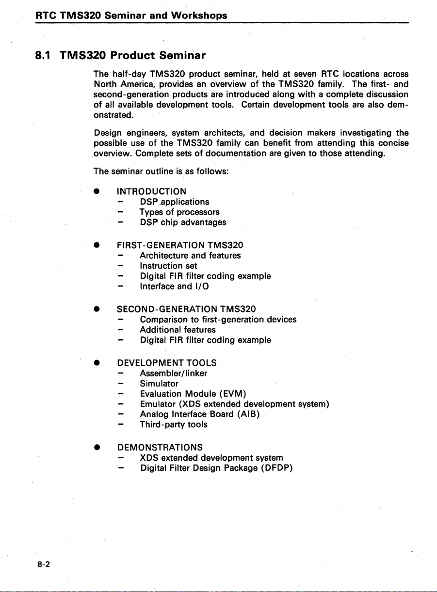
RTC
8.1
TMS320
TMS320
Seminar
Product
and
Workshops
Seminar
The half-day TMS320 product seminar, held at
an
North America, provides
second-generation products
of
all available development tools. Certain development tools
onstrated.
Design engineers, system architects, and decision makers investigating the
possible
. overview. Complete
The seminar
• INTRODUCTION
• FIRST-GENERATION TMS320
• SECOND-GENERATION TMS320
use
of
the TMS320 family
sets
outline
DSP
Types
DSP
Architecture
Instruction set
Digital
Interface
Comparison
Additional features
Digital
is
.applications
of
processors
chip advantages
FIR
and
FIR
overview
are
of
documentation
as
follows:
and
features
filter coding example
I/O
to
first-generation devices
filter coding example
of
the TMS320 family. The first-
introduced along with a complete discussion
can
benefit from attending this concise
are
seven
given
RTC
locations across
are
to
those attending.
al$o
dem-
and
8-2
• DEVELOPMENT TOOLS
• DEMONSTRATIONS
Assembler/linker
Simulator
Evaluation Module (EVM)
Emulator (XDS
Analog Interface Board
Third-party tools
'-
XDS extended development
Digital Filter Design
extended development
(AlB)
.Package
s~stem)
system
(DFDP)

RTe
TMS320
Seminar
and
Workshops
8.2 DSP
Design
The Regional Technology Centers (RTC) offer
Workshops, held either at the
development
sign for the first-generation processors and the other workshop for the second-generation devices.
The main objective
techniques for implementing current
signal processor. Exercises provide hands-on experience in
Topics covered in the First-Generation
• Using the TMS3201 0 Evaluation Module (EVM)
• First-generation architecture and instruction set
• Fractional binary arithmetic and scaling
• Coding
• First-generation development tools
• Hardware interfacing
• Subroutines and macros
• Implementation
The Second-Generation
neers in the early stages
velopment. The workshop enables the designer to more effectively use the
second-generation digital signal processors through hands-on practice
sign skills. He also
niques for application
assembly language programming and DSP knowledge
completion
in
Workshops
of
TMS320-based designs. One
of
the workshop
of
difference equations
of
is
introduced to numerous hardware and software tech-
of
of
the first-generation DSP workshop
this workshop include:
two
three-day DSP Design
RTC
location or
is
to
DSP algorithms using a TMS320 digital
DSP Design Workshop include:
a DTMF encoder.
DSP Design Workshop
of
TMS32020 and/or TMS320C25 application de-
current DSP algorithms. Previous experience
off~site,
of
demonstrate hardware and software
to assist users in the
the workshops supports de-
TMS320 design.
is
tailored for design engi-
is
necessary, and prior
is
desired. Topics covered
of
with
de-
• Using the second-generation TMS320 XDS emulator
• Second-generation architecture and instruction set
• Binary arithmetic, scaling, and difference equations
• Floating-point arithmetic
• System memory configurations
• Parallel interface timings
• Memory,
Class size for these workshops
the nearest
engineers from the same company enroll in the same course.
TI
I/O
interfacing, interrupts, and multiprocessing.
is
limited
to
ten students. To register, contact
RTC.
A 15-percent discount
is
available when three or more
with a PC
8-3

RTC
8.3
TMS320
RTC
Locations
Seminar
and
Workshops
Further information about the TMS320 product seminar and
can
be
Workshops
Center (RTC). The following list gives the worldwide locations
North
Atlanta
5515 Spalding Drive
Norcross, GA
(404)
Boston
400-2
Waltham,
(617) 895-9196
Chicago
515
Arlington Heights, I L 60005
(312) 640-2909
Canada
301
Mallorn Centre
Nepean
K2H9C4337
(613) 726-1970
American
662-7945
Totten Pond
MA
W.
Algonquin
Moodie Drive
(Ottawa), Canada
obtained by contacting the nearest Regional Technology
Locations:
Dallas
1001
E.
30092
02154
Road
Road
Campbell
Richardson,
(214) 680-5066
Northern
5353 Betsy
Santa
Clara,
748-2220
(408)
Southern
17891 Cartwright
Irvine, CA 92714
660-8140
(714)
Road
TX
75081
California
Ross
Drive
CA 95054
California
Road
of
DSP
the TI
Design
RTCs.
8-4
European
Denmark
Marielundvej 46 E
DK-2730 Herlev
Copenhagen, Denmark
45-2-917-400
France
8-10
Boite Postale 67
Velizy-Villacoublay Cedex
Paris, France
33-3-946-9712
Locations:
Avenue Morane Saulnier
Holland
P.O.
Box 12995
1100 AZ Amsterdam Zuid-Oost
Amsterdam, Holland
31-20-560-2911
Sweden
Norra Hamnvagen 3
39103
Box
54
S-100
Stockholm, Sweden
46-8-615-448

RTC
TMS320
Seminar
and
Workshops
Germany
Mexikoring
2000 Hamburg 60, Germany
49-40-220"2230
Kirchhorster Strasse 2
3000 Hannover 51, Germany
49-511
N.W.
Maybachstr,
7302 Ostfildern 2-Nellingen
N.W. Germany
49-711-34030
Asian
Osaka,
Nissho Iwai Bldg 5F
30 Imabashi 3-Chome
Higashi-Ku
81-6-204-1884
Tokyo,
Aoyama Fuji Bldg. 4F
6-12
Minato-Ku
81-3-498-2111
19
-648-021
Germany
11
locations:
Japan
Japan
Kita-Aoyama 3-Chome
541
107
Italy
Via
Ie
Europa,
20093 Cologno Monzese
Milano, Italy
39-2-253-2541
Viale Delle Scienze, 1
02014 Cittaducale
Rieti, Italy
39-746-6941
United
Manton Lane
Bedford, England MK417PA
0234-224-825
(44)
Nagoya,
Daini Toyota West Bldg. 7F
10-27
Nakamura-Ku
81-52-583-8691
38/44
Kingdom
Japan
Meieki 4-Chome
450
Hong-Kong
8th Floor, World Shipping Centre
Harbour City
Kowloon
852-3-7221223
7,
Canton Road
8-5

8-6

9.
TMS320
Documentation
Texas
Instruments provides extensive documentation
family from product announcement through applications development. Documents vary from brief product descriptions to user's guides, from application
reports
latest product and documentation updates
newsletter,
service. Technical questions regarding the
the TMS320 DSP hotline (see Section 9.9).
This section discusses the various documents listed below.
to
applications books, and from technical articles to textbooks. The
Details on Signal Processing, and the TMS320 DSP bulletin board
Support
to
support the TMS320
are
given in the TMS320 quarterly
TMS320 family may
be
directed
to
• Product Descriptions and Product Bulletins (Section
• User's Guides (Section 9.2 on page
• Data Sheets (Section 9.3 on page
•
DSP
Applications Book (Section 9.4 on page
• University Textbooks (Section 9.5 on page
• Technical Articles (Section 9.6 on page
• TMS320 Quarterly Newsletter (Section 9.7 on page
• TMS320 DSP Bulletin Board Service (Section 9.8 on page 9-24)
• TMS320 DSP Hotline (Section 9.9 on page
To receive copies
quest card at the back
-800-232-3200.
at 1
of
available TMS320 literature, complete the literature re-
of
this document or call the Customer Response Center
9-3)
9-4)
9-13)
9-16)
9-27)
9-5)
9.1
9-23)
on page
9-2)
9-1

Documentation
9.1
Product Descriptions and Prodoct Bulletins
Support
- Product Descriptions/Bulletins
Product descriptions and product bulletins
when
s new product
is
being announced. Later these documents
by the product user's guide.
A product description briefly describes the new device, presents key features
and block diagrams, and suggests applications. Product
ically published to give updated information on the
signal processors. Product descriptions
product
Table 9-1 lists
support the
bulletins.
the
product descriptions and product bulletins available to
TMS320 family. They can be ordered using the literature number
indicated.
are
the first documents published
are
bulletins
TMS320
are
longer and more detailed than
are
family
replaced
period-
of
digital
Table 9-1.
PRODUCT DOCUMENT NUMBER
TMS320C25 TMS320C25 Product Description
TMS320
TMS320
TMS320
Product
Digital Signal Processors Product Bulletin
Bulletins and
Product
Descriptions
LITERATURE
SPRVOO6
SPRT013
9-2

Documentation
Support - User's Guides
9.2 User's Guides
A user's guide for a TMS320 processor provides detailed information regarding the architecture
structions, and hardware and software applications. Table
guides
available for the TMS320 family
of
the device, its operation, assembly language
of
processors.
9-2
lists the user's
in-
Table 9-2.
PRODUCT
TMS32010 TMS32010 User's Guide SPRU001 B
TMS32011 TMS32011 User's Guide SPRU010
TMS32020 TMS32020
TMS320C25 TMS320C25 User's Guide SPRU012
TMS320 TMS320 Family
Guide
TMS320
DOCUMENT
User's Guide
Development Support Reference
User's Guides
LITERATURE
NUMBER
SPRUOO4B
SPRU011
9-3

Documentation
Support -
9.3' Data Sheets
The chief purpose
timing, and
of
the device architecture, a list
struction set summary. A data sheet may
appendix. Table
Data
Sheets
of
a data sheet
is
to
provide the electrical specifications,
mechanical data for the device.
of
key
features, a block diagram, and
9-3
lists the
TM5320
data sheets available.
It
also includes a brief description
be
included in a user's guide
an
as
in-
an
Table 9-3.
PRODUCT DOCUMENT NUMBER
TMS32010
TMS32010-14 TMS32010-14 Data Sheet SPRS008
TMS32011 TMS32011 Data Sheet SPRS005
TMS320C10 TMS320C10
TMS32020
TMS320C25 TMS320C25 Data Sheet
NOTE:
TllilS32010 Data Sheet SPRS02A
TMS32020
(included
The TMS32010-25 and TMS320C10-25 specifications
TMS32010 and TMS320C10 data sheets, respectively.
TM5320
Data Sheet
Data Sheet SPRS003A
in TMS320C25 User's Guide)
Data Sheets
LITERATURE
SPRS006
SPRS007
are
covered in the
9-4
Documentation
9.4
DSP Applications Book
Support -DSP
Applications Book
The TMS320 engineers
assist customers in designing
New application reports
Board Service (see Section 9.8) and in the TMS320 quarterly newsletter, De-
tails on Signal Processing.
Seventeen
munications, and computer applications,
book,
book combines
750-page volume, thus providing users a single source for finding information
on the most common
The
briefly introduces the device architectures, characteristics, support, and development tools for the first
part covers some
sponse (FIR) and Infinite Impulse Response (IIR) filters and
Transforms (FFT),
facing and
of
the book
lected and thoroughly discussed. These applications
egories: telecommunications, and computers and
speech coding/recognition, image/graphics, and digital control).
The materials included in this book
have geen generated by the DSP engineering staff
Semiconductor Group. Some published articles and a technical report have
been reprinted in the book to
to
provide completeness
more
TMS320
application reports, which cover generic DSP routines, telecom-
Digital
DSP Applications .Book
Signal Processing Applications
application reports on the TMS3201 0 and TMS32020 into a
multiprocessing
is
applications specific. Some typical DSP applications
complete theory and implementations (consisting
code,
and/or
are
constantly developing application reports
DSP applications using the TMS320 family.
ar~
announced through the TMS320 DSP Bulletin
are
included in the recently published
with
the TMS320 Family. This
applications
two
of
the common DSP routines, such
implemented. using the TMS320 devices. Hardware inter-
of
schematics) than the reprinted articles.
of
the TMS320 family.
is
divided into three major parts. The first part
generations
with
these devices
supplement the
the subject matter. The application reports contain
of
TMS320 processors. The second
as
Finite Impulse
are
also included. The last part
are
divided into
peripherals (including
are
primarily application reports,
of
Texas Instruments
17
application reports in order
of
as
they
Fast
Fourier
are
two
which
algorithms,
Re-
se-
cat-
Table
9-4
lists the application reports in the order in which they appear in the
Applications Book. The
application report.
following
subsections give a brief description
of
each
9-5

Documentation
Support -DSP
Applications
Book
Table 9-4.
APPLICATION
DSP
Routines
DSP
Interface
Telecommun ications TMS32010
Image/Graphics TMS32020
Digital Control
Included in the Applications Book
cussed. This code
Application
AREA
TMS32010/20
TMS32020
TMS32010/20
TMS32010
TMS32020 Floating-Point Arithmetic
TMS32010 Precis
TMS32010/20
TMS32010
TMS32010
TMS32020
TMS32020 MC68000 Interface
TMS32020
TMS32010
TMS32010 ADPCM (CCITT/Non-CCITT)
TMS32010 Control System Implementation
can
be
Reports
DEVICE
in
the
DSP Applications Book
FI
Rill
R Filters
FFT
Companding Routines
Floating-Point Arithmetic
jon
Generation
Matrix Multiplication
Asynchronous Input Interface
External Memory Interface
Hardware Interface
Telecommunications Interfaces
Digital Voice Echo Cancellation
Data Encryption
Graphics Implementation
is
the source code for the applications dis-
Digital Sine-Wave
used to reduce design .time and move
TMS320-based products to market faster. The routines
it
easy
software library making
applications.
See
Section 6.5 for a description
for users
to
apply the software to their
of
the
SUBJECT
are
also available in a
DSP
Software Library.
own
9.4.1
9-6
Implementation
Many signal processing applications require that digital filters
of
analog filters. Digital filters can meet
of
FIR/IIR
Filters
with
the
TMS32010/TMS32020
be
tight
specifications on magnitude and
phase characteristics and eliminate voltage drift. temperature drift. and noise
with
problems associated
This application report describes a variety
analog filter components.
of
methods for implementing Finite
Impulse Response (FIR) and Infinite Impulse Response (IIR) digital filters
with
the TMS320 family. , Emphasis
of
and the number
different structures
data memory locations required. Tradeoffs between several
of
the
two
TMS32010 source code examples implement
is
on minimizing both the execution time
classes
of
digital filters
two
are
also discussed.
FIR
filters and three IIR
ters (direct. cascade. and parallel) based on the techniques described in this
of
application report. Plots
unit sample response. and other pertinent data accompany
implementations. The methods presented
of
filters can
be
readily extended to any desired order
the frequency response. log-magnitude response.
each
'for implementing the different types
of
filter.
used in place
fil-
of
the filter
Documentation
Support -DSP.Applications
Book·
9.4.2
9.4.3
9.4.4
Fast
Fourier
Recent advances in VLSI hardware, such
have further enhanced the
This
the
processing.
This report discusses the
derivation
plementation aspects such
velopment,
direct and indirect memory addressing modes.
amples
024-point
1
implementing large
Companding
Companding
public and private telephone networks. The speed and versatility
TMS320 allow companding
This
panding methods.
can be performed using the
TMS32020.
Floating-Point
Transform
application report describes the implementation
TMS32020 processor that has features particularly suited
of
the
two
are
also given for a
complex
Routines
is
application report describes both the
Arithmetic
Algorithms
popularity
development
FFT
algorithm. Special attention
as
scaling. To expedite TMS32020
macro libraries
FFT,
along
FFTs.
for
the
required for applications that use codec devices, such
to
Sample programs
computational power
with
with
the
TMS32020
as
the TMS320 family
of
the
Fast
Fourier Transform (FFT).
of
of
the
OFT
algorithm, leading
is
given
are
included in the appendices for both the
TMS32020 source code ex-
256-point
with
(both radix-2 and radix-4) and a
some system memory considerations for
TMS32010/TMS32020
be performed in either software or hardware.
are
the
TMS32010
A-law
included to show
and IJ-Iaw software com-
of
the TMS3201 0 and the
of
processors,
FFT
algorithms using
to
digital signal
to
various
FFT
how
companding
to
the
FFT
im-
code de-
as
of
the
in
9.4.5
This application report analyzes
multiplication on the TMS32010. The floating-point single-precision
and
standard proposed by the
the
TMS32010 performs a floating-point multiplication in 8.4 microseconds
and a
speeds
For illustration
a choice between different
arithmetic notation and
Floating-Point
In this application report,
plication,
single-precision standard proposed
floating-point multiplication in 7.8 microseconds, a floating-point addition in
15.4 microseconds, and a
A review
sion algorithms
floating-point addition in 17.2 microseconds. These computation
are
comparable to dedicated floating-point processors.
of
floating-point formats and the tradeoffs involved in making
of
Arithmetic
and division on the
of
floating.-point notation and
is
also presented.
an
implementation
IEEE
is specifically examined. Using this standard,
floating-point formats, a review
addition and multiplication algorithms
with
the
TMS32020
an
implementation
TMS32020
floating-point division in 22.8 microseconds.
is
analyzed. Using the floating-point
by
the
IEEE,
of
addition, multiplication, and
of
floating-point addition
of
of
floating-point addition, multi-
the TMS32020 performs a
floating-point
is
presented.
divi-
9-7
 Loading...