


现货库存、技术资料、百科信息、热点资讯,精彩尽在鼎好!
TMS320R2811, TMS320R2812
Digital Signal Processors
Data Manual
Literature Number: SPRS257
June 2004
ADVANCE INFORMATION concerns new
products in the sampling or preproduction
phase of development. Characteristic data and
other specifications are subject to change
without notice.

IMPORTANT NOTICE
Texas Instruments Incorporated and its subsidiaries (TI) reserve the right to make corrections, modifications,
enhancements, improvements, and other changes to its products and services at any time and to discontinue
any product or service without notice. Customers should obtain the latest relevant information before placing
orders and should verify that such information is current and complete. All products are sold subject to TI’s terms
and conditions of sale supplied at the time of order acknowledgment.
TI warrants performance of its hardware products to the specifications applicable at the time of sale in
accordance with TI’s standard warranty. Testing and other quality control techniques are used to the extent TI
deems necessary to support this warranty . Except where mandated by government requirements, testing of all
parameters of each product is not necessarily performed.
TI assumes no liability for applications assistance or customer product design. Customers are responsible for
their products and applications using TI components. To minimize the risks associated with customer products
and applications, customers should provide adequate design and operating safeguards.
TI does not warrant or represent that any license, either express or implied, is granted under any TI patent right,
copyright, mask work right, or other TI intellectual property right relating to any combination, machine, or process
in which TI products or services are used. Information published by TI regarding third-party products or services
does not constitute a license from TI to use such products or services or a warranty or endorsement thereof.
Use of such information may require a license from a third party under the patents or other intellectual property
of the third party, or a license from TI under the patents or other intellectual property of TI.
Reproduction of information in TI data books or data sheets is permissible only if reproduction is without
alteration and is accompanied by all associated warranties, conditions, limitations, and notices. Reproduction
of this information with alteration is an unfair and deceptive business practice. TI is not responsible or liable for
such altered documentation.
Resale of TI products or services with statements different from or beyond the parameters stated by TI for that
product or service voids all express and any implied warranties for the associated TI product or service and
is an unfair and deceptive business practice. TI is not responsible or liable for any such statements.
Following are URLs where you can obtain information on other Texas Instruments products and application
solutions:
Products Applications
Amplifiers amplifier.ti.com Audio www.ti.com/audio
Data Converters dataconverter.ti.com Automotive www.ti.com/automotive
DSP dsp.ti.com Broadband www.ti.com/broadband
Interface interface.ti.com Digital Control www.ti.com/digitalcontrol
Logic logic.ti.com Military www.ti.com/military
Power Mgmt power.ti.com Optical Networking www.ti.com/opticalnetwork
Microcontrollers microcontroller.ti.com Security www.ti.com/security
Telephony www.ti.com/telephony
Video & Imaging www.ti.com/video
Wireless www.ti.com/wireless
Mailing Address: Texas Instruments
Post Office Box 655303 Dallas, Texas 75265
Copyright 2004, Texas Instruments Incorporated

Contents
Contents
Section Page
1 Features 11. . . . . . . . . . . . . . . . . . . . . . . . . . . . . . . . . . . . . . . . . . . . . . . . . . . . . . . . . . . . . . . . . . . . . . . . . . . . . . . . .
2 Introduction 12. . . . . . . . . . . . . . . . . . . . . . . . . . . . . . . . . . . . . . . . . . . . . . . . . . . . . . . . . . . . . . . . . . . . . . . . . . . . .
2.1 Description 12. . . . . . . . . . . . . . . . . . . . . . . . . . . . . . . . . . . . . . . . . . . . . . . . . . . . . . . . . . . . . . . . . . . . . .
2.2 Device Summary 13. . . . . . . . . . . . . . . . . . . . . . . . . . . . . . . . . . . . . . . . . . . . . . . . . . . . . . . . . . . . . . . .
2.3 Pin Assignments 14. . . . . . . . . . . . . . . . . . . . . . . . . . . . . . . . . . . . . . . . . . . . . . . . . . . . . . . . . . . . . . . . .
2.3.1 Terminal Assignments for the GHH and ZHH Packages 14. . . . . . . . . . . . . . . . . . .
2.3.2 Pin Assignments for the PGF Package 15. . . . . . . . . . . . . . . . . . . . . . . . . . . . . . . . . .
2.3.3 Pin Assignments for the PBK Package 16. . . . . . . . . . . . . . . . . . . . . . . . . . . . . . . . . .
2.4 Signal Descriptions 17. . . . . . . . . . . . . . . . . . . . . . . . . . . . . . . . . . . . . . . . . . . . . . . . . . . . . . . . . . . . . . .
3 Functional Overview 27. . . . . . . . . . . . . . . . . . . . . . . . . . . . . . . . . . . . . . . . . . . . . . . . . . . . . . . . . . . . . . . . . . . . .
3.1 Memory Map 28. . . . . . . . . . . . . . . . . . . . . . . . . . . . . . . . . . . . . . . . . . . . . . . . . . . . . . . . . . . . . . . . . . . .
3.2 Brief Descriptions 31. . . . . . . . . . . . . . . . . . . . . . . . . . . . . . . . . . . . . . . . . . . . . . . . . . . . . . . . . . . . . . . .
3.2.1 C28x CPU 31. . . . . . . . . . . . . . . . . . . . . . . . . . . . . . . . . . . . . . . . . . . . . . . . . . . . . . . . . .
3.2.2 Memory Bus (Harvard Bus Architecture) 31. . . . . . . . . . . . . . . . . . . . . . . . . . . . . . . .
3.2.3 Peripheral Bus 32. . . . . . . . . . . . . . . . . . . . . . . . . . . . . . . . . . . . . . . . . . . . . . . . . . . . . . .
3.2.4 Real-Time JTAG and Analysis 32. . . . . . . . . . . . . . . . . . . . . . . . . . . . . . . . . . . . . . . . .
3.2.5 External Interface (XINTF) (2812 Only) 32. . . . . . . . . . . . . . . . . . . . . . . . . . . . . . . . .
3.2.6 M0, M1 SARAMs 32. . . . . . . . . . . . . . . . . . . . . . . . . . . . . . . . . . . . . . . . . . . . . . . . . . . .
3.2.7 L0, L1, L2, L3, H0 SARAMs 32. . . . . . . . . . . . . . . . . . . . . . . . . . . . . . . . . . . . . . . . . . .
3.2.8 Boot ROM 33. . . . . . . . . . . . . . . . . . . . . . . . . . . . . . . . . . . . . . . . . . . . . . . . . . . . . . . . . .
3.2.9 Security 33. . . . . . . . . . . . . . . . . . . . . . . . . . . . . . . . . . . . . . . . . . . . . . . . . . . . . . . . . . . . .
3.2.10 Peripheral Interrupt Expansion (PIE) Block 33. . . . . . . . . . . . . . . . . . . . . . . . . . . . . .
3.2.11 External Interrupts (XINT1, 2, 13, XNMI) 33. . . . . . . . . . . . . . . . . . . . . . . . . . . . . . . .
3.2.12 Oscillator and PLL 33. . . . . . . . . . . . . . . . . . . . . . . . . . . . . . . . . . . . . . . . . . . . . . . . . . .
3.2.13 Watchdog 33. . . . . . . . . . . . . . . . . . . . . . . . . . . . . . . . . . . . . . . . . . . . . . . . . . . . . . . . . . .
3.2.14 Peripheral Clocking 33. . . . . . . . . . . . . . . . . . . . . . . . . . . . . . . . . . . . . . . . . . . . . . . . . . .
3.2.15 Low-Power Modes 34. . . . . . . . . . . . . . . . . . . . . . . . . . . . . . . . . . . . . . . . . . . . . . . . . . .
3.2.16 Peripheral Frames 0, 1, 2 (PFn) 34. . . . . . . . . . . . . . . . . . . . . . . . . . . . . . . . . . . . . . . .
3.2.17 General-Purpose Input/Output (GPIO) Multiplexer 34. . . . . . . . . . . . . . . . . . . . . . . .
3.2.18 32-Bit CPU-Timers (0, 1, 2) 34. . . . . . . . . . . . . . . . . . . . . . . . . . . . . . . . . . . . . . . . . . . .
3.2.19 Control Peripherals 35. . . . . . . . . . . . . . . . . . . . . . . . . . . . . . . . . . . . . . . . . . . . . . . . . . .
3.2.20 Serial Port Peripherals 35. . . . . . . . . . . . . . . . . . . . . . . . . . . . . . . . . . . . . . . . . . . . . . . .
3.3 Register Map 35. . . . . . . . . . . . . . . . . . . . . . . . . . . . . . . . . . . . . . . . . . . . . . . . . . . . . . . . . . . . . . . . . . . .
3.4 Device Emulation Registers 37. . . . . . . . . . . . . . . . . . . . . . . . . . . . . . . . . . . . . . . . . . . . . . . . . . . . . . .
3.5 External Interface, XINTF (2812 Only) 38. . . . . . . . . . . . . . . . . . . . . . . . . . . . . . . . . . . . . . . . . . . . . .
3.5.1 Timing Registers 39. . . . . . . . . . . . . . . . . . . . . . . . . . . . . . . . . . . . . . . . . . . . . . . . . . . . .
3.5.2 XREVISION Register 39. . . . . . . . . . . . . . . . . . . . . . . . . . . . . . . . . . . . . . . . . . . . . . . . .
3.6 Interrupts 40. . . . . . . . . . . . . . . . . . . . . . . . . . . . . . . . . . . . . . . . . . . . . . . . . . . . . . . . . . . . . . . . . . . . . . .
3.6.1 External Interrupts 43. . . . . . . . . . . . . . . . . . . . . . . . . . . . . . . . . . . . . . . . . . . . . . . . . . .
3.7 System Control 44. . . . . . . . . . . . . . . . . . . . . . . . . . . . . . . . . . . . . . . . . . . . . . . . . . . . . . . . . . . . . . . . . .
3.7.1 OSC and PLL Block 45. . . . . . . . . . . . . . . . . . . . . . . . . . . . . . . . . . . . . . . . . . . . . . . . . .
3.7.2 Loss of Input Clock 46. . . . . . . . . . . . . . . . . . . . . . . . . . . . . . . . . . . . . . . . . . . . . . . . . . .
3.7.3 PLL-Based Clock Module 47. . . . . . . . . . . . . . . . . . . . . . . . . . . . . . . . . . . . . . . . . . . . .
3.7.4 External Reference Oscillator Clock Option 47. . . . . . . . . . . . . . . . . . . . . . . . . . . . . .
3.7.5 Watchdog Block 48. . . . . . . . . . . . . . . . . . . . . . . . . . . . . . . . . . . . . . . . . . . . . . . . . . . . .
3.7.6 Low-Power Modes Block 48. . . . . . . . . . . . . . . . . . . . . . . . . . . . . . . . . . . . . . . . . . . . . .
4 Peripherals 50. . . . . . . . . . . . . . . . . . . . . . . . . . . . . . . . . . . . . . . . . . . . . . . . . . . . . . . . . . . . . . . . . . . . . . . . . . . . . .
4.1 32-Bit CPU-Timers 0/1/2 50. . . . . . . . . . . . . . . . . . . . . . . . . . . . . . . . . . . . . . . . . . . . . . . . . . . . . . . . . .
June 2004 SPRS257
3

Contents
4.2 Event Manager Modules (EVA, EVB) 52. . . . . . . . . . . . . . . . . . . . . . . . . . . . . . . . . . . . . . . . . . . . . . .
4.2.1 General-Purpose (GP) Timers 55. . . . . . . . . . . . . . . . . . . . . . . . . . . . . . . . . . . . . . . . .
4.2.2 Full-Compare Units 56. . . . . . . . . . . . . . . . . . . . . . . . . . . . . . . . . . . . . . . . . . . . . . . . . . .
4.2.3 Programmable Deadband Generator 56. . . . . . . . . . . . . . . . . . . . . . . . . . . . . . . . . . . .
4.2.4 PWM Waveform Generation 56. . . . . . . . . . . . . . . . . . . . . . . . . . . . . . . . . . . . . . . . . . .
4.2.5 Double Update PWM Mode 56. . . . . . . . . . . . . . . . . . . . . . . . . . . . . . . . . . . . . . . . . . . .
4.2.6 PWM Characteristics 56. . . . . . . . . . . . . . . . . . . . . . . . . . . . . . . . . . . . . . . . . . . . . . . . .
4.2.7 Capture Unit 57. . . . . . . . . . . . . . . . . . . . . . . . . . . . . . . . . . . . . . . . . . . . . . . . . . . . . . . . .
4.2.8 Quadrature-Encoder Pulse (QEP) Circuit 57. . . . . . . . . . . . . . . . . . . . . . . . . . . . . . . .
4.2.9 External ADC Start-of-Conversion 57. . . . . . . . . . . . . . . . . . . . . . . . . . . . . . . . . . . . . .
4.3 Enhanced Analog-to-Digital Converter (ADC) Module 58. . . . . . . . . . . . . . . . . . . . . . . . . . . . . . . . .
4.4 Enhanced Controller Area Network (eCAN) Module 63. . . . . . . . . . . . . . . . . . . . . . . . . . . . . . . . . . .
4.5 Multichannel Buffered Serial Port (McBSP) Module 67. . . . . . . . . . . . . . . . . . . . . . . . . . . . . . . . . . .
4.6 Serial Communications Interface (SCI) Module 70. . . . . . . . . . . . . . . . . . . . . . . . . . . . . . . . . . . . . . .
4.7 Serial Peripheral Interface (SPI) Module 73. . . . . . . . . . . . . . . . . . . . . . . . . . . . . . . . . . . . . . . . . . . .
4.8 GPIO MUX 77. . . . . . . . . . . . . . . . . . . . . . . . . . . . . . . . . . . . . . . . . . . . . . . . . . . . . . . . . . . . . . . . . . . . . .
5 Development Support 80. . . . . . . . . . . . . . . . . . . . . . . . . . . . . . . . . . . . . . . . . . . . . . . . . . . . . . . . . . . . . . . . . . . .
5.1 Device and Development Support Tool Nomenclature 80. . . . . . . . . . . . . . . . . . . . . . . . . . . . . . . . .
5.2 Documentation Support 81. . . . . . . . . . . . . . . . . . . . . . . . . . . . . . . . . . . . . . . . . . . . . . . . . . . . . . . . . . .
6 Electrical Specifications 84. . . . . . . . . . . . . . . . . . . . . . . . . . . . . . . . . . . . . . . . . . . . . . . . . . . . . . . . . . . . . . . . . .
6.1 Absolute Maximum Ratings 84. . . . . . . . . . . . . . . . . . . . . . . . . . . . . . . . . . . . . . . . . . . . . . . . . . . . . . .
6.2 Recommended Operating Conditions 85. . . . . . . . . . . . . . . . . . . . . . . . . . . . . . . . . . . . . . . . . . . . . . .
6.3 Electrical Characteristics Over Recommended Operating Conditions
(Unless Otherwise Noted) 85. . . . . . . . . . . . . . . . . . . . . . . . . . . . . . . . . . . . . . . . . . . . . . . . . . . . . . . . .
6.4 Current Consumption by Power-Supply Pins Over Recommended Operating Conditions
During Low-Power Modes at 150-MHz SYSCLKOUT (TMS320R281x) 86. . . . . . . . . . . . . . . . . .
6.5 Current Consumption Graphs 87. . . . . . . . . . . . . . . . . . . . . . . . . . . . . . . . . . . . . . . . . . . . . . . . . . . . . .
6.6 Reducing Current Consumption 87. . . . . . . . . . . . . . . . . . . . . . . . . . . . . . . . . . . . . . . . . . . . . . . . . . . .
6.7 Power Sequencing Requirements 87. . . . . . . . . . . . . . . . . . . . . . . . . . . . . . . . . . . . . . . . . . . . . . . . . .
6.8 Signal Transition Levels 88. . . . . . . . . . . . . . . . . . . . . . . . . . . . . . . . . . . . . . . . . . . . . . . . . . . . . . . . . . .
6.9 Timing Parameter Symbology 89. . . . . . . . . . . . . . . . . . . . . . . . . . . . . . . . . . . . . . . . . . . . . . . . . . . . .
6.10 General Notes on Timing Parameters 89. . . . . . . . . . . . . . . . . . . . . . . . . . . . . . . . . . . . . . . . . . . . . . .
6.11 Test Load Circuit 89. . . . . . . . . . . . . . . . . . . . . . . . . . . . . . . . . . . . . . . . . . . . . . . . . . . . . . . . . . . . . . . . .
6.12 Device Clock Table 90. . . . . . . . . . . . . . . . . . . . . . . . . . . . . . . . . . . . . . . . . . . . . . . . . . . . . . . . . . . . . . .
6.13 Clock Requirements and Characteristics 90. . . . . . . . . . . . . . . . . . . . . . . . . . . . . . . . . . . . . . . . . . . .
6.13.1 Input Clock Requirements 90. . . . . . . . . . . . . . . . . . . . . . . . . . . . . . . . . . . . . . . . . . . . .
6.13.2 Output Clock Characteristics 92. . . . . . . . . . . . . . . . . . . . . . . . . . . . . . . . . . . . . . . . . .
6.14 Reset Timing 92. . . . . . . . . . . . . . . . . . . . . . . . . . . . . . . . . . . . . . . . . . . . . . . . . . . . . . . . . . . . . . . . . . . .
6.15 Low-Power Mode Wakeup Timing 97. . . . . . . . . . . . . . . . . . . . . . . . . . . . . . . . . . . . . . . . . . . . . . . . . .
6.16 Event Manager Interface 100. . . . . . . . . . . . . . . . . . . . . . . . . . . . . . . . . . . . . . . . . . . . . . . . . . . . . . . . .
6.16.1 PWM Timing 100. . . . . . . . . . . . . . . . . . . . . . . . . . . . . . . . . . . . . . . . . . . . . . . . . . . . . . .
6.16.2 Interrupt Timing 102. . . . . . . . . . . . . . . . . . . . . . . . . . . . . . . . . . . . . . . . . . . . . . . . . . . . .
6.17 General-Purpose Input/Output (GPIO) − Output Timing 103. . . . . . . . . . . . . . . . . . . . . . . . . . . . . .
6.18 General-Purpose Input/Output (GPIO) − Input Timing 104. . . . . . . . . . . . . . . . . . . . . . . . . . . . . . . .
6.19 SPI Master Mode Timing 105. . . . . . . . . . . . . . . . . . . . . . . . . . . . . . . . . . . . . . . . . . . . . . . . . . . . . . . . .
6.20 SPI Slave Mode Timing 109. . . . . . . . . . . . . . . . . . . . . . . . . . . . . . . . . . . . . . . . . . . . . . . . . . . . . . . . . .
6.21 External Interface (XINTF) Timing 112. . . . . . . . . . . . . . . . . . . . . . . . . . . . . . . . . . . . . . . . . . . . . . . . .
6.22 XINTF Signal Alignment to XCLKOUT 114. . . . . . . . . . . . . . . . . . . . . . . . . . . . . . . . . . . . . . . . . . . . .
6.23 External Interface Read Timing 116. . . . . . . . . . . . . . . . . . . . . . . . . . . . . . . . . . . . . . . . . . . . . . . . . . .
6.24 External Interface Write Timing 117. . . . . . . . . . . . . . . . . . . . . . . . . . . . . . . . . . . . . . . . . . . . . . . . . . .
4
June 2004SPRS257

Contents
6.25 External Interface Ready-on-Read Timing With One External Wait State 118. . . . . . . . . . . . . . . .
6.26 External Interface Ready-on-Write Timing With One External Wait State 121. . . . . . . . . . . . . . . .
6.27 XHOLD
and XHOLDA 124. . . . . . . . . . . . . . . . . . . . . . . . . . . . . . . . . . . . . . . . . . . . . . . . . . . . . . . . . . .
6.28 XHOLD/XHOLDA Timing 125. . . . . . . . . . . . . . . . . . . . . . . . . . . . . . . . . . . . . . . . . . . . . . . . . . . . . . . . .
6.29 On-Chip Analog-to-Digital Converter 127. . . . . . . . . . . . . . . . . . . . . . . . . . . . . . . . . . . . . . . . . . . . . . .
6.29.1 ADC Absolute Maximum Ratings† 127. . . . . . . . . . . . . . . . . . . . . . . . . . . . . . . . . . . . .
6.29.2 ADC Electrical Characteristics Over Recommended
Operating Conditions 128. . . . . . . . . . . . . . . . . . . . . . . . . . . . . . . . . . . . . . . . . . . . . . . .
6.29.3 Current Consumption for Different ADC Configurations
(at 25-MHz ADCCLK) 129. . . . . . . . . . . . . . . . . . . . . . . . . . . . . . . . . . . . . . . . . . . . . . . .
6.29.4 ADC Power-Up Control Bit Timing 130. . . . . . . . . . . . . . . . . . . . . . . . . . . . . . . . . . . . .
6.29.5 Detailed Description 131. . . . . . . . . . . . . . . . . . . . . . . . . . . . . . . . . . . . . . . . . . . . . . . . .
6.29.6 Sequential Sampling Mode (Single-Channel) (SMODE = 0) 131. . . . . . . . . . . . . . .
6.29.7 Simultaneous Sampling Mode (Dual-Channel) (SMODE = 1) 133. . . . . . . . . . . . . .
6.29.8 Definitions of Specifications and Terminology 134. . . . . . . . . . . . . . . . . . . . . . . . . . .
6.30 Multichannel Buffered Serial Port (McBSP) Timing 135. . . . . . . . . . . . . . . . . . . . . . . . . . . . . . . . . . .
6.30.1 McBSP Transmit and Receive Timing 135. . . . . . . . . . . . . . . . . . . . . . . . . . . . . . . . . .
6.30.2 McBSP as SPI Master or Slave Timing 138. . . . . . . . . . . . . . . . . . . . . . . . . . . . . . . . .
7 Migration From F281x Devices 142. . . . . . . . . . . . . . . . . . . . . . . . . . . . . . . . . . . . . . . . . . . . . . . . . . . . . . . . . . .
8 Mechanical Data 144. . . . . . . . . . . . . . . . . . . . . . . . . . . . . . . . . . . . . . . . . . . . . . . . . . . . . . . . . . . . . . . . . . . . . . . .
8.1 Ball Grid Array (BGA) 144. . . . . . . . . . . . . . . . . . . . . . . . . . . . . . . . . . . . . . . . . . . . . . . . . . . . . . . . . . .
8.2 Plastic Ball Grid Array 145. . . . . . . . . . . . . . . . . . . . . . . . . . . . . . . . . . . . . . . . . . . . . . . . . . . . . . . . . . .
8.3 Low-Profile Quad Flatpacks (LQFPs) 146. . . . . . . . . . . . . . . . . . . . . . . . . . . . . . . . . . . . . . . . . . . . . .
June 2004 SPRS257
5

Figures
List of Figures
Figure Page
Figure 2−1. TMS320R2812 179-Ball GHH and ZHH MicroStar BGA (Bottom View) 14. . . . . . . . . . . . . . . . . . . . . .
Figure 2−2. TMS320R2812 176-Pin PGF LQFP (Top View) 15. . . . . . . . . . . . . . . . . . . . . . . . . . . . . . . . . . . . . . . . . . .
Figure 2−3. TMS320R2811 128-Pin PBK LQFP (Top View) 16. . . . . . . . . . . . . . . . . . . . . . . . . . . . . . . . . . . . . . . . . . .
Figure 3−1. Functional Block Diagram 27. . . . . . . . . . . . . . . . . . . . . . . . . . . . . . . . . . . . . . . . . . . . . . . . . . . . . . . . . . . . .
Figure 3−2. R2812 Memory Map 28. . . . . . . . . . . . . . . . . . . . . . . . . . . . . . . . . . . . . . . . . . . . . . . . . . . . . . . . . . . . . . . . . .
Figure 3−3. R2811 Memory Map 29. . . . . . . . . . . . . . . . . . . . . . . . . . . . . . . . . . . . . . . . . . . . . . . . . . . . . . . . . . . . . . . . . .
Figure 3−4. External Interface Block Diagram 38. . . . . . . . . . . . . . . . . . . . . . . . . . . . . . . . . . . . . . . . . . . . . . . . . . . . . . .
Figure 3−5. Interrupt Sources 40. . . . . . . . . . . . . . . . . . . . . . . . . . . . . . . . . . . . . . . . . . . . . . . . . . . . . . . . . . . . . . . . . . . . .
Figure 3−6. Multiplexing of Interrupts Using the PIE Block 41. . . . . . . . . . . . . . . . . . . . . . . . . . . . . . . . . . . . . . . . . . . .
Figure 3−7. Clock and Reset Domains 44. . . . . . . . . . . . . . . . . . . . . . . . . . . . . . . . . . . . . . . . . . . . . . . . . . . . . . . . . . . . .
Figure 3−8. OSC and PLL Block 46. . . . . . . . . . . . . . . . . . . . . . . . . . . . . . . . . . . . . . . . . . . . . . . . . . . . . . . . . . . . . . . . . .
Figure 3−9. Recommended Crystal/Clock Connection 47. . . . . . . . . . . . . . . . . . . . . . . . . . . . . . . . . . . . . . . . . . . . . . . .
Figure 3−10. Watchdog Module 48. . . . . . . . . . . . . . . . . . . . . . . . . . . . . . . . . . . . . . . . . . . . . . . . . . . . . . . . . . . . . . . . . . .
Figure 4−1. CPU-Timers 50. . . . . . . . . . . . . . . . . . . . . . . . . . . . . . . . . . . . . . . . . . . . . . . . . . . . . . . . . . . . . . . . . . . . . . . . .
Figure 4−2. CPU-Timer Interrupts Signals and Output Signal 51. . . . . . . . . . . . . . . . . . . . . . . . . . . . . . . . . . . . . . . . . .
Figure 4−3. Event Manager A Functional Block Diagram 55. . . . . . . . . . . . . . . . . . . . . . . . . . . . . . . . . . . . . . . . . . . . .
Figure 4−4. Block Diagram of the R281x ADC Module 59. . . . . . . . . . . . . . . . . . . . . . . . . . . . . . . . . . . . . . . . . . . . . . .
Figure 4−5. ADC Pin Connections With Internal Reference 60. . . . . . . . . . . . . . . . . . . . . . . . . . . . . . . . . . . . . . . . . . .
Figure 4−6. ADC Pin Connections With External Reference 61. . . . . . . . . . . . . . . . . . . . . . . . . . . . . . . . . . . . . . . . . . .
Figure 4−7. eCAN Block Diagram and Interface Circuit 64. . . . . . . . . . . . . . . . . . . . . . . . . . . . . . . . . . . . . . . . . . . . . . .
Figure 4−8. eCAN Memory Map 65. . . . . . . . . . . . . . . . . . . . . . . . . . . . . . . . . . . . . . . . . . . . . . . . . . . . . . . . . . . . . . . . . .
Figure 4−9. McBSP Module With FIFO 68. . . . . . . . . . . . . . . . . . . . . . . . . . . . . . . . . . . . . . . . . . . . . . . . . . . . . . . . . . . .
Figure 4−10. Serial Communications Interface (SCI) Module Block Diagram 72. . . . . . . . . . . . . . . . . . . . . . . . . . . .
Figure 4−11. Serial Peripheral Interface Module Block Diagram (Slave Mode) 76. . . . . . . . . . . . . . . . . . . . . . . . . . .
Figure 4−12. Modes of Operation 79. . . . . . . . . . . . . . . . . . . . . . . . . . . . . . . . . . . . . . . . . . . . . . . . . . . . . . . . . . . . . . . . .
Figure 5−1. TMS320x28x Device Nomenclature 81. . . . . . . . . . . . . . . . . . . . . . . . . . . . . . . . . . . . . . . . . . . . . . . . . . . . .
Figure 6−1. R2812/R2811 Typical Current Consumption (With Peripheral Clocks Enabled) 87. . . . . . . . . . . . . . . .
Figure 6−2. Output Levels 88. . . . . . . . . . . . . . . . . . . . . . . . . . . . . . . . . . . . . . . . . . . . . . . . . . . . . . . . . . . . . . . . . . . . . . . .
Figure 6−3. Input Levels 88. . . . . . . . . . . . . . . . . . . . . . . . . . . . . . . . . . . . . . . . . . . . . . . . . . . . . . . . . . . . . . . . . . . . . . . . .
Figure 6−4. 3.3-V Test Load Circuit 89. . . . . . . . . . . . . . . . . . . . . . . . . . . . . . . . . . . . . . . . . . . . . . . . . . . . . . . . . . . . . . . .
Figure 6−5. Clock Timing 92. . . . . . . . . . . . . . . . . . . . . . . . . . . . . . . . . . . . . . . . . . . . . . . . . . . . . . . . . . . . . . . . . . . . . . . . .
Figure 6−6. Power-on Reset in Microcomputer Mode (XMP/MC = 0) 93. . . . . . . . . . . . . . . . . . . . . . . . . . . . . . . . . . .
Figure 6−7. Power-on Reset in Microprocessor Mode (XMP/MC = 1) 94. . . . . . . . . . . . . . . . . . . . . . . . . . . . . . . . . . .
Figure 6−8. Warm Reset in Microcomputer Mode 95. . . . . . . . . . . . . . . . . . . . . . . . . . . . . . . . . . . . . . . . . . . . . . . . . . . .
Figure 6−9. Effect of Writing Into PLLCR Register 96. . . . . . . . . . . . . . . . . . . . . . . . . . . . . . . . . . . . . . . . . . . . . . . . . . .
Figure 6−10. IDLE Entry and Exit Timing 97. . . . . . . . . . . . . . . . . . . . . . . . . . . . . . . . . . . . . . . . . . . . . . . . . . . . . . . . . . .
Figure 6−11. STANDBY Entry and Exit Timing 98. . . . . . . . . . . . . . . . . . . . . . . . . . . . . . . . . . . . . . . . . . . . . . . . . . . . . .
Figure 6−12. HALT Wakeup Using XNMI 99. . . . . . . . . . . . . . . . . . . . . . . . . . . . . . . . . . . . . . . . . . . . . . . . . . . . . . . . . . .
Figure 6−13. PWM Output Timing 100. . . . . . . . . . . . . . . . . . . . . . . . . . . . . . . . . . . . . . . . . . . . . . . . . . . . . . . . . . . . . . . .
Figure 6−14. TDIRx Timing 100. . . . . . . . . . . . . . . . . . . . . . . . . . . . . . . . . . . . . . . . . . . . . . . . . . . . . . . . . . . . . . . . . . . . . .
6
June 2004SPRS257

Figure 6−15. EVASOC Timing 101. . . . . . . . . . . . . . . . . . . . . . . . . . . . . . . . . . . . . . . . . . . . . . . . . . . . . . . . . . . . . . . . . . .
Figure 6−16. EVBSOC Timing 101. . . . . . . . . . . . . . . . . . . . . . . . . . . . . . . . . . . . . . . . . . . . . . . . . . . . . . . . . . . . . . . . . . .
Figure 6−17. External Interrupt Timing 103. . . . . . . . . . . . . . . . . . . . . . . . . . . . . . . . . . . . . . . . . . . . . . . . . . . . . . . . . . . .
Figure 6−18. General-Purpose Output Timing 103. . . . . . . . . . . . . . . . . . . . . . . . . . . . . . . . . . . . . . . . . . . . . . . . . . . . . .
Figure 6−19. GPIO Input Qualifier − Example Diagram for QUALPRD = 1 104. . . . . . . . . . . . . . . . . . . . . . . . . . . . .
Figure 6−20. General-Purpose Input Timing 104. . . . . . . . . . . . . . . . . . . . . . . . . . . . . . . . . . . . . . . . . . . . . . . . . . . . . . .
Figure 6−21. SPI Master Mode External Timing (Clock Phase = 0) 106. . . . . . . . . . . . . . . . . . . . . . . . . . . . . . . . . . . .
Figure 6−22. SPI Master External Timing (Clock Phase = 1) 108. . . . . . . . . . . . . . . . . . . . . . . . . . . . . . . . . . . . . . . . .
Figure 6−23. SPI Slave Mode External Timing (Clock Phase = 0) 110. . . . . . . . . . . . . . . . . . . . . . . . . . . . . . . . . . . . .
Figure 6−24. SPI Slave Mode External Timing (Clock Phase = 1) 111. . . . . . . . . . . . . . . . . . . . . . . . . . . . . . . . . . . . .
Figure 6−25. Relationship Between XTIMCLK and SYSCLKOUT 114. . . . . . . . . . . . . . . . . . . . . . . . . . . . . . . . . . . . .
Figure 6−26. Example Read Access 116. . . . . . . . . . . . . . . . . . . . . . . . . . . . . . . . . . . . . . . . . . . . . . . . . . . . . . . . . . . . . .
Figure 6−27. Example Write Access 117. . . . . . . . . . . . . . . . . . . . . . . . . . . . . . . . . . . . . . . . . . . . . . . . . . . . . . . . . . . . . .
Figure 6−28. Example Read With Synchronous XREADY Access 119. . . . . . . . . . . . . . . . . . . . . . . . . . . . . . . . . . . .
Figure 6−29. Example Read With Asynchronous XREADY Access 120. . . . . . . . . . . . . . . . . . . . . . . . . . . . . . . . . . .
Figure 6−30. Write With Synchronous XREADY Access 122. . . . . . . . . . . . . . . . . . . . . . . . . . . . . . . . . . . . . . . . . . . . .
Figure 6−31. Write With Asynchronous XREADY Access 123. . . . . . . . . . . . . . . . . . . . . . . . . . . . . . . . . . . . . . . . . . . .
Figure 6−32. External Interface Hold Waveform 125. . . . . . . . . . . . . . . . . . . . . . . . . . . . . . . . . . . . . . . . . . . . . . . . . . . .
Figure 6−33. XHOLD
/XHOLDA Timing Requirements (XCLKOUT = 1/2 XTIMCLK) 126. . . . . . . . . . . . . . . . . . . . .
Figure 6−34. ADC Analog Input Impedance Model 130. . . . . . . . . . . . . . . . . . . . . . . . . . . . . . . . . . . . . . . . . . . . . . . . . .
Figure 6−35. ADC Power-Up Control Bit Timing 130. . . . . . . . . . . . . . . . . . . . . . . . . . . . . . . . . . . . . . . . . . . . . . . . . . . .
Figure 6−36. Sequential Sampling Mode (Single-Channel) Timing 132. . . . . . . . . . . . . . . . . . . . . . . . . . . . . . . . . . . .
Figure 6−37. Simultaneous Sampling Mode Timing 133. . . . . . . . . . . . . . . . . . . . . . . . . . . . . . . . . . . . . . . . . . . . . . . . .
Figure 6−38. McBSP Receive Timing 137. . . . . . . . . . . . . . . . . . . . . . . . . . . . . . . . . . . . . . . . . . . . . . . . . . . . . . . . . . . . .
Figure 6−39. McBSP Transmit Timing 137. . . . . . . . . . . . . . . . . . . . . . . . . . . . . . . . . . . . . . . . . . . . . . . . . . . . . . . . . . . . .
Figure 6−40. McBSP Timing as SPI Master or Slave: CLKSTP = 10b, CLKXP = 0 138. . . . . . . . . . . . . . . . . . . . . .
Figure 6−41. McBSP Timing as SPI Master or Slave: CLKSTP = 11b, CLKXP = 0 139. . . . . . . . . . . . . . . . . . . . . .
Figure 6−42. McBSP Timing as SPI Master or Slave: CLKSTP = 10b, CLKXP = 1 140. . . . . . . . . . . . . . . . . . . . . .
Figure 6−43. McBSP Timing as SPI Master or Slave: CLKSTP = 11b, CLKXP = 1 141. . . . . . . . . . . . . . . . . . . . . .
Figure 7−1. TMS320R2812 179-Ball GHH MicroStar BGA 144. . . . . . . . . . . . . . . . . . . . . . . . . . . . . . . . . . . . . . . . . . .
Figure 7−2. TMS320R2812 179-Ball ZHH MicroStar BGA 145. . . . . . . . . . . . . . . . . . . . . . . . . . . . . . . . . . . . . . . . . . .
Figure 7−3. TMS320R2812 176-Pin PGF LQFP 146. . . . . . . . . . . . . . . . . . . . . . . . . . . . . . . . . . . . . . . . . . . . . . . . . . . .
Figure 7−4. TMS320R2811 128-Pin PBK LQFP 147. . . . . . . . . . . . . . . . . . . . . . . . . . . . . . . . . . . . . . . . . . . . . . . . . . . .
Figures
June 2004 SPRS257
7

Tables
List of Tables
Table Page
Table 2−1. Hardware Features 13. . . . . . . . . . . . . . . . . . . . . . . . . . . . . . . . . . . . . . . . . . . . . . . . . . . . . . . . . . . . . . . . . . . .
Table 2−2. Signal Descriptions 17. . . . . . . . . . . . . . . . . . . . . . . . . . . . . . . . . . . . . . . . . . . . . . . . . . . . . . . . . . . . . . . . . . .
Table 3−1. Wait States 31. . . . . . . . . . . . . . . . . . . . . . . . . . . . . . . . . . . . . . . . . . . . . . . . . . . . . . . . . . . . . . . . . . . . . . . . . . .
Table 3−2. Peripheral Frame 0 Registers 36. . . . . . . . . . . . . . . . . . . . . . . . . . . . . . . . . . . . . . . . . . . . . . . . . . . . . . . . . . .
Table 3−3. Peripheral Frame 1 Registers 36. . . . . . . . . . . . . . . . . . . . . . . . . . . . . . . . . . . . . . . . . . . . . . . . . . . . . . . . . . .
Table 3−4. Peripheral Frame 2 Registers 36. . . . . . . . . . . . . . . . . . . . . . . . . . . . . . . . . . . . . . . . . . . . . . . . . . . . . . . . . . .
Table 3−5. Device Emulation Registers 37. . . . . . . . . . . . . . . . . . . . . . . . . . . . . . . . . . . . . . . . . . . . . . . . . . . . . . . . . . . .
Table 3−6. XINTF Configuration and Control Register Mappings 39. . . . . . . . . . . . . . . . . . . . . . . . . . . . . . . . . . . . . . .
Table 3−7. XREVISION Register Bit Definitions 39. . . . . . . . . . . . . . . . . . . . . . . . . . . . . . . . . . . . . . . . . . . . . . . . . . . . .
Table 3−8. PIE Peripheral Interrupts 41. . . . . . . . . . . . . . . . . . . . . . . . . . . . . . . . . . . . . . . . . . . . . . . . . . . . . . . . . . . . . . .
Table 3−9. PIE Configuration and Control Registers 42. . . . . . . . . . . . . . . . . . . . . . . . . . . . . . . . . . . . . . . . . . . . . . . . . .
Table 3−10. External Interrupt Registers 43. . . . . . . . . . . . . . . . . . . . . . . . . . . . . . . . . . . . . . . . . . . . . . . . . . . . . . . . . . . .
Table 3−11. PLL, Clocking, Watchdog, and Low-Power Mode Registers 45. . . . . . . . . . . . . . . . . . . . . . . . . . . . . . . .
Table 3−12. PLLCR Register Bit Definitions 46. . . . . . . . . . . . . . . . . . . . . . . . . . . . . . . . . . . . . . . . . . . . . . . . . . . . . . . . .
Table 3−13. Possible PLL Configuration Modes 47. . . . . . . . . . . . . . . . . . . . . . . . . . . . . . . . . . . . . . . . . . . . . . . . . . . . .
Table 3−14. R281x Low-Power Modes 49. . . . . . . . . . . . . . . . . . . . . . . . . . . . . . . . . . . . . . . . . . . . . . . . . . . . . . . . . . . . .
Table 4−1. CPU-Timers 0, 1, 2 Configuration and Control Registers 52. . . . . . . . . . . . . . . . . . . . . . . . . . . . . . . . . . . .
Table 4−2. Module and Signal Names for EVA and EVB 53. . . . . . . . . . . . . . . . . . . . . . . . . . . . . . . . . . . . . . . . . . . . . .
Table 4−3. EVA Registers 54. . . . . . . . . . . . . . . . . . . . . . . . . . . . . . . . . . . . . . . . . . . . . . . . . . . . . . . . . . . . . . . . . . . . . . . .
Table 4−4. ADC Registers 62. . . . . . . . . . . . . . . . . . . . . . . . . . . . . . . . . . . . . . . . . . . . . . . . . . . . . . . . . . . . . . . . . . . . . . . .
Table 4−5. 3.3-V eCAN Transceivers for the R281x DSPs 64. . . . . . . . . . . . . . . . . . . . . . . . . . . . . . . . . . . . . . . . . . . .
Table 4−6. CAN Registers Map 66. . . . . . . . . . . . . . . . . . . . . . . . . . . . . . . . . . . . . . . . . . . . . . . . . . . . . . . . . . . . . . . . . . .
Table 4−7. McBSP Register Summary 69. . . . . . . . . . . . . . . . . . . . . . . . . . . . . . . . . . . . . . . . . . . . . . . . . . . . . . . . . . . . .
Table 4−8. SCI-A Registers 73. . . . . . . . . . . . . . . . . . . . . . . . . . . . . . . . . . . . . . . . . . . . . . . . . . . . . . . . . . . . . . . . . . . . . . .
Table 4−9. SCI-B Registers 73. . . . . . . . . . . . . . . . . . . . . . . . . . . . . . . . . . . . . . . . . . . . . . . . . . . . . . . . . . . . . . . . . . . . . . .
Table 4−10. SPI Registers 75. . . . . . . . . . . . . . . . . . . . . . . . . . . . . . . . . . . . . . . . . . . . . . . . . . . . . . . . . . . . . . . . . . . . . . . .
Table 4−11. GPIO Mux Registers 77. . . . . . . . . . . . . . . . . . . . . . . . . . . . . . . . . . . . . . . . . . . . . . . . . . . . . . . . . . . . . . . . . .
Table 4−12. GPIO Data Registers 78. . . . . . . . . . . . . . . . . . . . . . . . . . . . . . . . . . . . . . . . . . . . . . . . . . . . . . . . . . . . . . . . .
Table 6−1. Typical Current Consumption by Various Peripherals (at 150 MHz) 87. . . . . . . . . . . . . . . . . . . . . . . . . . .
Table 6−2. TMS320R281x Clock Table and Nomenclature 90. . . . . . . . . . . . . . . . . . . . . . . . . . . . . . . . . . . . . . . . . . . .
Table 6−3. Input Clock Frequency 90. . . . . . . . . . . . . . . . . . . . . . . . . . . . . . . . . . . . . . . . . . . . . . . . . . . . . . . . . . . . . . . . .
Table 6−4. XCLKIN Timing Requirements − PLL Bypassed or Enabled 91. . . . . . . . . . . . . . . . . . . . . . . . . . . . . . . . .
Table 6−5. XCLKIN Timing Requirements − PLL Disabled 91. . . . . . . . . . . . . . . . . . . . . . . . . . . . . . . . . . . . . . . . . . . .
Table 6−6. Possible PLL Configuration Modes 91. . . . . . . . . . . . . . . . . . . . . . . . . . . . . . . . . . . . . . . . . . . . . . . . . . . . . .
Table 6−7. XCLKOUT Switching Characteristics (PLL Bypassed or Enabled) 92. . . . . . . . . . . . . . . . . . . . . . . . . . . .
Table 6−8. Reset (XRS) Timing Requirements 92. . . . . . . . . . . . . . . . . . . . . . . . . . . . . . . . . . . . . . . . . . . . . . . . . . . . . .
Table 6−9. IDLE Mode Switching Characteristics 97. . . . . . . . . . . . . . . . . . . . . . . . . . . . . . . . . . . . . . . . . . . . . . . . . . . .
Table 6−10. STANDBY Mode Switching Characteristics 97. . . . . . . . . . . . . . . . . . . . . . . . . . . . . . . . . . . . . . . . . . . . . .
Table 6−11. HALT Mode Switching Characteristics 98. . . . . . . . . . . . . . . . . . . . . . . . . . . . . . . . . . . . . . . . . . . . . . . . . . .
Table 6−12. PWM Switching Characteristics 100. . . . . . . . . . . . . . . . . . . . . . . . . . . . . . . . . . . . . . . . . . . . . . . . . . . . . . .
Table 6−13. Timer and Capture Unit Timing Requirements 100. . . . . . . . . . . . . . . . . . . . . . . . . . . . . . . . . . . . . . . . . . .
Table 6−14. External ADC Start-of-Conversion − EVA − Switching Characteristics 101. . . . . . . . . . . . . . . . . . . . . .
Table 6−15. External ADC Start-of-Conversion − EVB − Switching Characteristics 101. . . . . . . . . . . . . . . . . . . . . .
Table 6−16. Interrupt Switching Characteristics 102. . . . . . . . . . . . . . . . . . . . . . . . . . . . . . . . . . . . . . . . . . . . . . . . . . . . .
Table 6−17. Interrupt Timing Requirements 102. . . . . . . . . . . . . . . . . . . . . . . . . . . . . . . . . . . . . . . . . . . . . . . . . . . . . . . .
Table 6−18. General-Purpose Output Switching Characteristics 103. . . . . . . . . . . . . . . . . . . . . . . . . . . . . . . . . . . . . .
8
June 2004SPRS257

Table 6−19. General-Purpose Input Timing Requirements 104. . . . . . . . . . . . . . . . . . . . . . . . . . . . . . . . . . . . . . . . . . .
Table 6−20. SPI Master Mode External Timing (Clock Phase = 0) 105. . . . . . . . . . . . . . . . . . . . . . . . . . . . . . . . . . . . .
Table 6−21. SPI Master Mode External Timing (Clock Phase = 1) 107. . . . . . . . . . . . . . . . . . . . . . . . . . . . . . . . . . . . .
Table 6−22. SPI Slave Mode External Timing (Clock Phase = 0) 109. . . . . . . . . . . . . . . . . . . . . . . . . . . . . . . . . . . . . .
Table 6−23. SPI Slave Mode External Timing (Clock Phase = 1) 111. . . . . . . . . . . . . . . . . . . . . . . . . . . . . . . . . . . . . .
Table 6−24. Relationship Between Parameters Configured in XTIMING and Duration of Pulse 112. . . . . . . . . . . .
Table 6−25. XINTF Clock Configurations 114. . . . . . . . . . . . . . . . . . . . . . . . . . . . . . . . . . . . . . . . . . . . . . . . . . . . . . . . . .
Table 6−26. External Memory Interface Read Switching Characteristics 116. . . . . . . . . . . . . . . . . . . . . . . . . . . . . . .
Table 6−27. External Memory Interface Read Timing Requirements 116. . . . . . . . . . . . . . . . . . . . . . . . . . . . . . . . . . .
Table 6−28. External Memory Interface Write Switching Characteristics 117. . . . . . . . . . . . . . . . . . . . . . . . . . . . . . .
Table 6−29. External Memory Interface Read Switching Characteristics
(Ready-on-Read, 1 Wait State) 118. . . . . . . . . . . . . . . . . . . . . . . . . . . . . . . . . . . . . . . . . . . . . . . . . . . . . . . . . .
Table 6−30. External Memory Interface Read Timing Requirements (Ready-on-Read, 1 Wait State) 118. . . . . .
Table 6−31. Synchronous XREADY Timing Requirements (Ready-on-Read, 1 Wait State) 118. . . . . . . . . . . . . . .
Table 6−32. Asynchronous XREADY Timing Requirements (Ready-on-Read, 1 Wait State) 118. . . . . . . . . . . . . .
Table 6−33. External Memory Interface Write Switching Characteristics (Ready-on-Write, 1 Wait State) 121. . .
Table 6−34. Synchronous XREADY Timing Requirements (Ready-on-Write, 1 Wait State) 121. . . . . . . . . . . . . . .
Table 6−35. Asynchronous XREADY Timing Requirements (Ready-on-Write, 1 Wait State) 121. . . . . . . . . . . . . .
Table 6−36. XHOLD
/XHOLDA Timing Requirements (XCLKOUT = XTIMCLK) 125. . . . . . . . . . . . . . . . . . . . . . . . .
Table 6−37. XHOLD/XHOLDA Timing Requirements (XCLKOUT = 1/2 XTIMCLK) 126. . . . . . . . . . . . . . . . . . . . . .
Table 6−38. DC Specifications 128. . . . . . . . . . . . . . . . . . . . . . . . . . . . . . . . . . . . . . . . . . . . . . . . . . . . . . . . . . . . . . . . . . .
Table 6−39. AC Specifications 129. . . . . . . . . . . . . . . . . . . . . . . . . . . . . . . . . . . . . . . . . . . . . . . . . . . . . . . . . . . . . . . . . . .
Table 6−40. ADC Power-Up Delays 130. . . . . . . . . . . . . . . . . . . . . . . . . . . . . . . . . . . . . . . . . . . . . . . . . . . . . . . . . . . . . . .
Table 6−41. Sequential Sampling Mode Timing 132. . . . . . . . . . . . . . . . . . . . . . . . . . . . . . . . . . . . . . . . . . . . . . . . . . . . .
Table 6−42. Simultaneous Sampling Mode Timing 133. . . . . . . . . . . . . . . . . . . . . . . . . . . . . . . . . . . . . . . . . . . . . . . . . .
Table 6−43. McBSP Timing Requirements 135. . . . . . . . . . . . . . . . . . . . . . . . . . . . . . . . . . . . . . . . . . . . . . . . . . . . . . . . .
Table 6−44. McBSP Switching Characteristics 136. . . . . . . . . . . . . . . . . . . . . . . . . . . . . . . . . . . . . . . . . . . . . . . . . . . . .
Table 6−45. McBSP as SPI Master or Slave Timing Requirements (CLKSTP = 10b, CLKXP = 0) 138. . . . . . . . .
Table 6−46. McBSP as SPI Master or Slave Switching Characteristics (CLKSTP = 10b, CLKXP = 0) 138. . . . . .
Table 6−47. McBSP as SPI Master or Slave Timing Requirements (CLKSTP = 11b, CLKXP = 0) 139. . . . . . . . . .
Table 6−48. McBSP as SPI Master or Slave Switching Characteristics (CLKSTP = 11b, CLKXP = 0) 139. . . . . .
Table 6−49. McBSP as SPI Master or Slave Timing Requirements (CLKSTP = 10b, CLKXP = 1) 140. . . . . . . . .
Table 6−50. McBSP as SPI Master or Slave Switching Characteristics (CLKSTP = 10b, CLKXP = 1) 140. . . . . .
Table 6−51. McBSP as SPI Master or Slave Timing Requirements (CLKSTP = 11b, CLKXP = 1) 141. . . . . . . . . .
Table 6−52. McBSP as SPI Master or Slave Switching Characteristics (CLKSTP = 11b, CLKXP = 1) 141. . . . . .
Table 6−53. Feature Comparison Between F281x and R281x Devices 142. . . . . . . . . . . . . . . . . . . . . . . . . . . . . . . . .
Table 7−1. Thermal Resistance Characteristics for 179-GHH 144. . . . . . . . . . . . . . . . . . . . . . . . . . . . . . . . . . . . . . . . .
Table 7−2. Thermal Resistance Characteristics for 179-ZHH 145. . . . . . . . . . . . . . . . . . . . . . . . . . . . . . . . . . . . . . . . .
Table 7−3. Thermal Resistance Characteristics for 176-PGF 146. . . . . . . . . . . . . . . . . . . . . . . . . . . . . . . . . . . . . . . . .
Table 7−4. Thermal Resistance Characteristics for 128-PBK 147. . . . . . . . . . . . . . . . . . . . . . . . . . . . . . . . . . . . . . . . .
Tables
June 2004 SPRS257
9

This page intentionally left blank.
10
June 2004SPRS257

1 Features
ADVANCE INFORMATION
Features
D High-Performance Static CMOS Technology
− 150 MHz (6.67-ns Cycle Time)
− Low-Power (1.8-V Core @135 MHz, 1.9-V
Core @150 MHz, 3.3-V I/O) Design
D JTAG Boundary Scan Support
†
D High-Performance 32-Bit CPU
(TMS320C28x)
− 16 x 16 and 32 x 32 MAC Operations
− 16 x 16 Dual MAC
− Harvard Bus Architecture
− Atomic Operations
− Fast Interrupt Response and Processing
− Unified Memory Programming Model
− 4M Linear Program/Data Address Reach
− Code-Efficient (in C/C++ and Assembly)
− Code and Pin Compatible to F2810,
F2811, and F2812 devices
− TMS320F24x/LF240x Processor Source
Code Compatible
D On-Chip Memory
− 20K x 16 Total Single-Access RAM
(SARAM)
− L0 and L1: 2 Blocks of 4K x 16 Each
SARAM
− L2 and L3: 2 Blocks of 1K X 16 SARAM
− H0: 1 Block of 8K x 16 SARAM
− M0 and M1: 2 Blocks of 1K x 16 Each
SARAM
D SPI, SCI, and GPIO Boot Loader Modes to
Support Loading Code From Off-chip
Sources to On-chip RAM. SPI Boot Mode
Supports Loading From an External Serial
EEPROM.
D Boot ROM (4K x 16)
− With Software Boot Modes
− Standard Math Tables
D External Interface (2812)
− Up to 1M Total Memory
− Programmable Wait States
− Programmable Read/Write Strobe Timing
− Three Individual Chip Selects
D Clock and System Control
− Dynamic PLL Ratio Changes Supported
− On-Chip Oscillator
− Watchdog Timer Module
D Three External Interrupts
D Peripheral Interrupt Expansion (PIE) Block
That Supports 45 Peripheral Interrupts
D Three 32-Bit CPU-Timers
D Motor Control Peripherals
− Two Event Managers (EVA, EVB)
− Compatible to 240xA Devices
D Serial Port Peripherals
− Serial Peripheral Interface (SPI)
− Two Serial Communications Interfaces
(SCIs), Standard UART
− Enhanced Controller Area Network
(eCAN)
− Multichannel Buffered Serial Port
(McBSP)
D 12-Bit ADC, 16 Channels
− 2 x 8 Channel Input Multiplexer
− Two Sample-and-Hold
− Single/Simultaneous Conversions
− Fast Conversion Rate: 80 ns/12.5 MSPS
D Up to 56 General Purpose I/O (GPIO) Pins
D Advanced Emulation Features
− Analysis and Breakpoint Functions
− Real-Time Debug via Hardware
D Development Tools Include
− ANSI C/C++ Compiler/Assembler/Linker
− Code Composer Studio IDE
− DSP/BIOS
− JTAG Scan Controllers
†
D Low-Power Modes and Power Savings
− IDLE, STANDBY, HALT Modes Supported
− Disable Individual Peripheral Clocks
D Package Options
− 179-Ball MicroStar BGA With External
Memory Interface (GHH), (ZHH) (2812)
− 176-Pin Low-Profile Quad Flatpack
(LQFP) With External Memory Interface
(PGF) (2812)
− 128-Pin LQFP Without External Memory
Interface (PBK) (2811)
D Temperature Options:
− A: −40°C to 85°C (GHH, ZHH, PGF, PBK)
− S/Q: −40°C to 125°C (GHH, ZHH, PGF,
PBK)
TMS320C24x, Code Composer Studio, DSP/BIOS, and MicroStar BGA are trademarks of Texas Instruments.
†
IEEE Standard 1149.1−1990, IEEE Standard Test-Access Port
June 2004 SPRS257
11

Introduction
ADVANCE INFORMATION
2 Introduction
This section provides a summary of each device’s features, lists the pin assignments, and describes the
function of each pin. This document also provides detailed descriptions of peripherals, electrical
specifications, parameter measurement information, and mechanical data about the available packaging.
2.1 Description
The TMS320R2811 and TMS320R2812 devices, members of the TMS320C28x DSP generation, are highly
integrated, high-performance solutions for demanding control applications. The functional blocks and the
memory maps are described in Section 3, Functional Overview.
Throughout this document, TMS320R2811 and TMS320R2812 are abbreviated as R2811 and R2812,
respectively.
TMS320C28x is a trademark of Texas Instruments.
All trademarks are the property of their respective owners.
12
June 2004SPRS257

2.2 Device Summary
ADVANCE INFORMATION
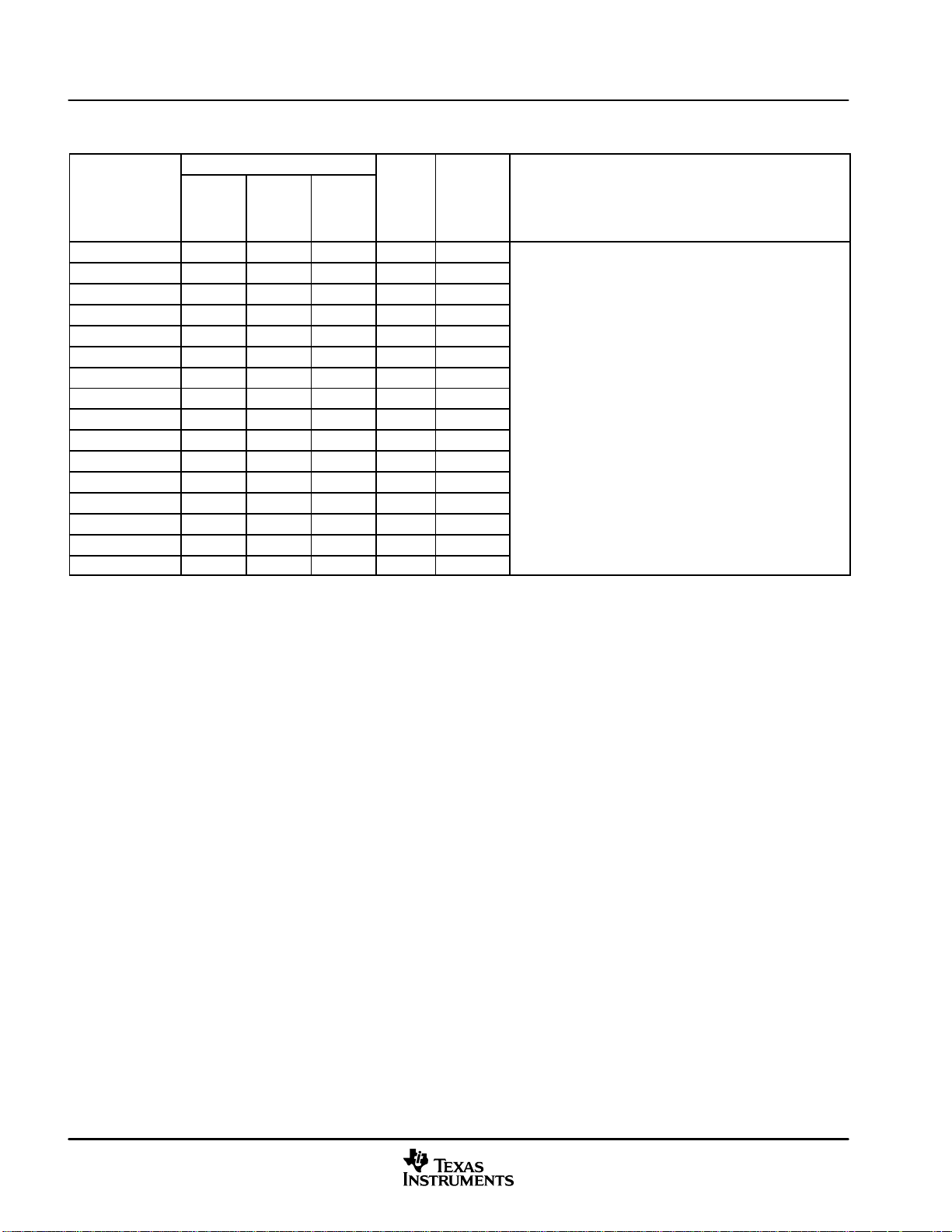
Table 2−1 provides a summary of each device’s features.
Table 2−1. Hardware Features
Introduction
†
FEATURE
Instruction Cycle (at 150 MHz) 6.67 ns 6.67 ns
Single-Access RAM (SARAM)
(16-bit word)
Boot ROM Yes Yes
External Memory Interface — Yes
Event Managers A and B
(EVA and EVB)
S General-Purpose (GP) Timers 4 4
S Compare (CMP)/PWM 16 16
S Capture (CAP)/QEP Channels 6/2 6/2
Watchdog Timer Yes Ye s
12-Bit ADC Ye s Ye s
S Channels 16 16
32-Bit CPU Timers 3 3
SPI Ye s Ye s
SCIA, SCIB SCIA, SCIB SCIA, SCIB
CAN Ye s Ye s
McBSP Yes Ye s
Digital I/O Pins (Shared) 56 56
External Interrupts 3 3
Supply Voltage 1.8-V Core, (135 MHz) 1.9-V Core (150 MHz), 3.3-V I/O
Packaging 128-pin PBK
Temperature Options
Product Status
†
The S temperature option has been replaced by the Q temperature option (40°C to 125°C) from silicon revision E onwards. Q stands for
−40°C to 125°C Q100 automotive fault grading.
‡
See Section 5.1, Device and Development Support Nomenclature for descriptions of TMS and TMX stages.
†
‡
A: −40°C to 85°C Yes Yes
S/Q: −40°C to 125°C Ye s Ye s
R2811 R2812
20K 20K
EVA, EVB EVA, EVB
179-ball GHH
179-ball ZHH
176-pin PGF
TMX TMX
June 2004 SPRS257
13
Introduction
ADVANCE INFORMATION
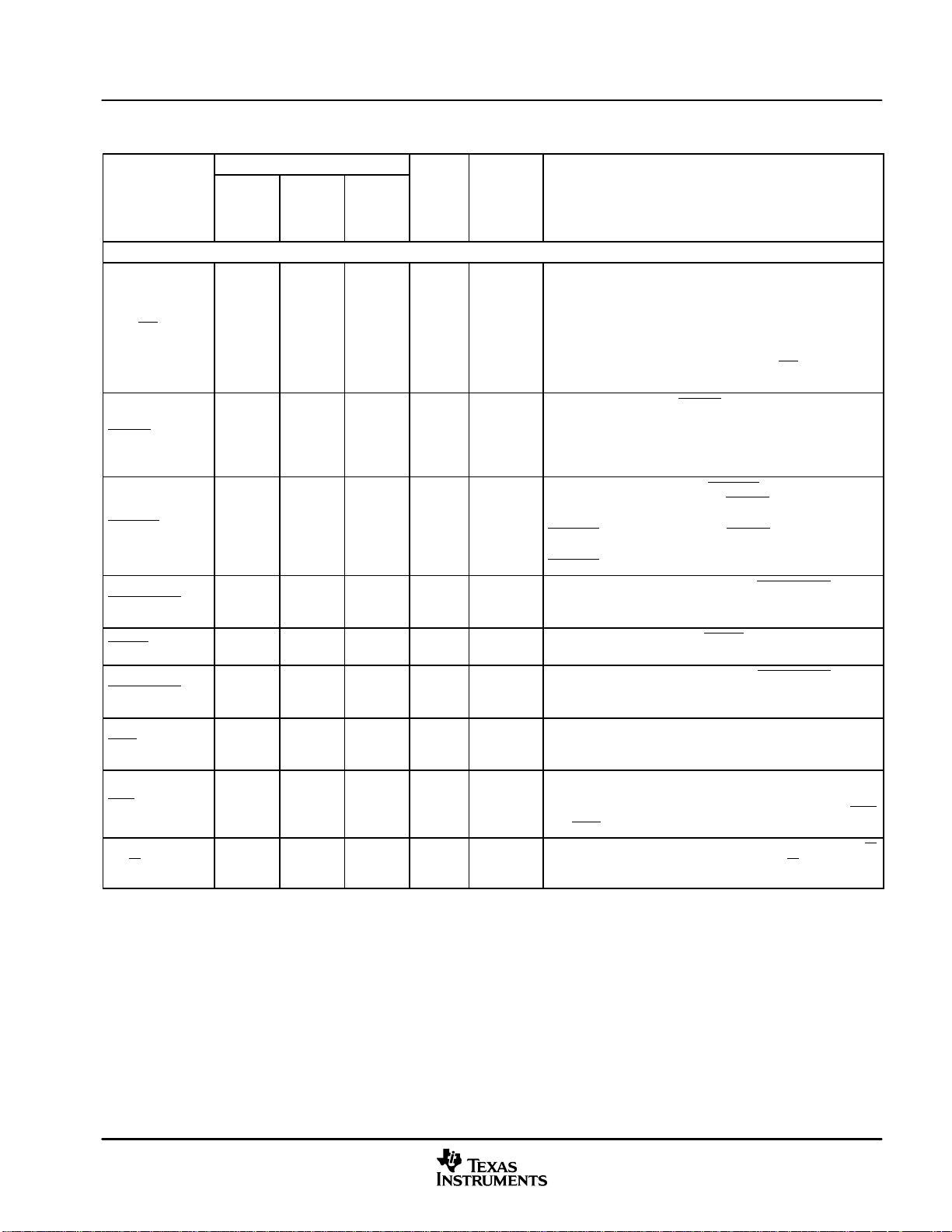
2.3 Pin Assignments
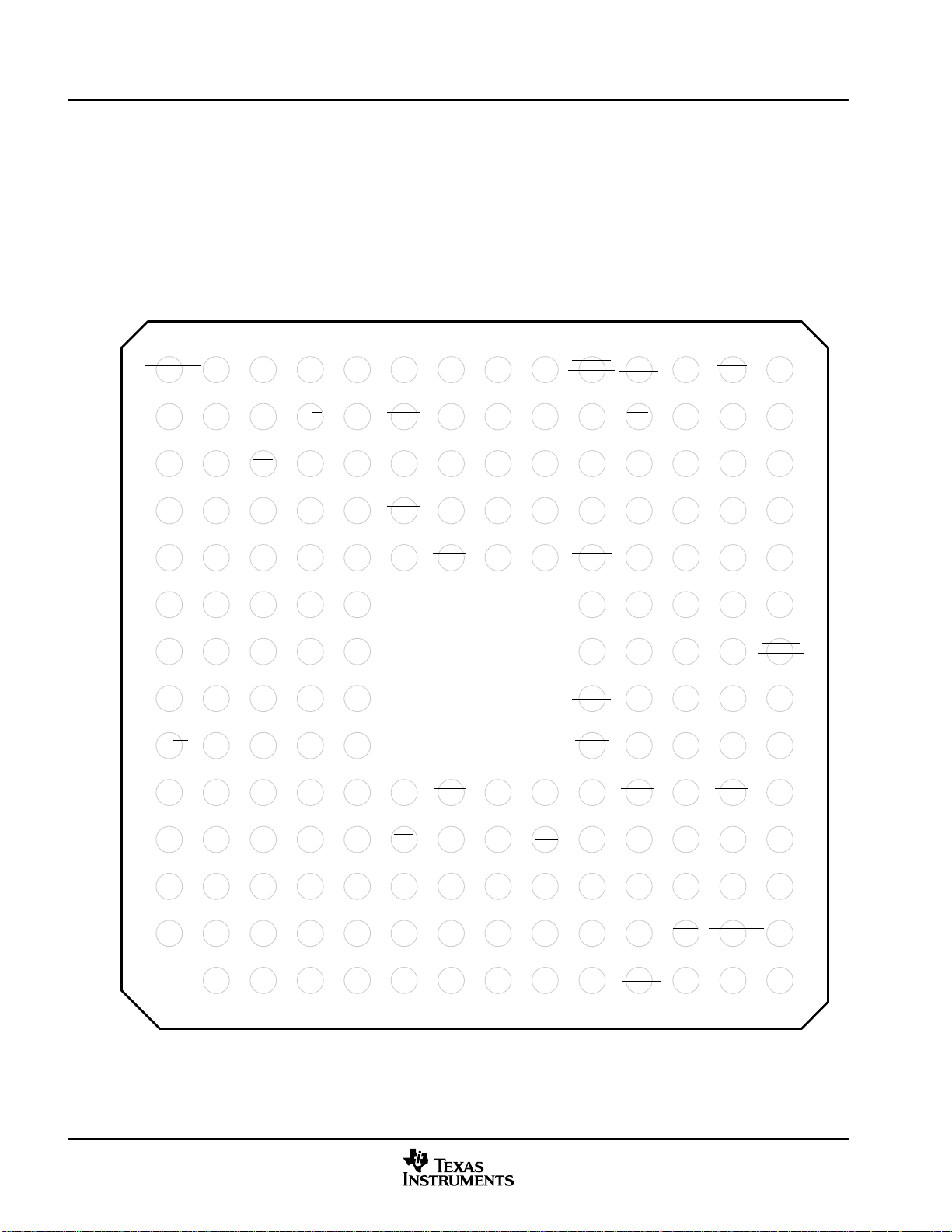
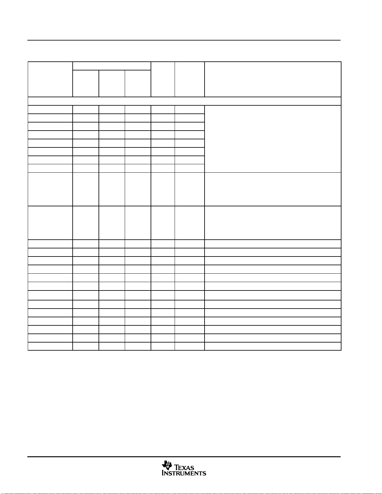
Figure 2−1 illustrates the ball locations for the 179-ball GHH and ZHH ball grid array (BGA) packages.
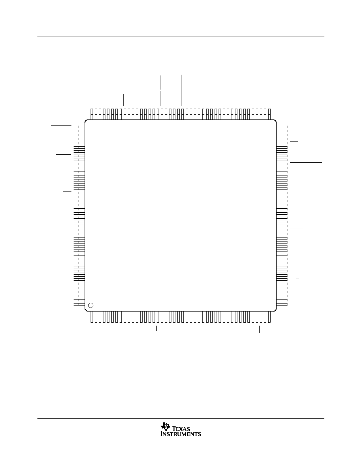
Figure 2−2 shows the pin assignments for the 176-pin PGF low-profile quad flatpack (LQFP) and Figure 2−3
shows the pin assignments for the 128-pin PBK LQFP. Table 2−2 describes the function(s) of each pin.
2.3.1 Terminal Assignments for the GHH and ZHH Packages
See Table 2−2 for a description of each terminal’s function(s).
P
N
M
XZCS0AND1 PWM10
SPISOMIA PWM9 XR/W
SPISIMOA XA[1] XRD
L
K
J
MCLKXA MFSRA XD[3]
H
G
F
E
MDXA MDRA XD[0]
XMP/MC
AVDD-
REFBG
PWM8
PWM7 TEST2
V
DD
V
SPICLKA
SS
V
MCLKRA XD[1] MFSXA XD[2]
DD
RESEXT
ADCREFP
XD[6] PWM11 XD[7] C5TRIP
V
SS
XD[4]
ADC-
V
AVSS-
REFBG
V
PWM12
SPISTEA
V
DDIO
V
V
SSA1
DDA1
ADCREFM ADCINA5
SS
T4PWM
_T4CMP
_QEP3
T3PWM
_T3CMP
SS
ADCINB7 C3TRIP XCLKOUT XA[7] TCLKINA TDIRA
CAP6
V
DD
_QEPI2
C4TRIP
CAP4
CAP5
_QEP4
XD[5] XD[13]
XA[0]
BGREFIN
XD[8]
TEST1 XD[9] X2
V
V
C6TRIP TCLKINB
SS
ADC-
XHOLD
DDIO
V
SS
V
DDIO
TDIRB XD[10]
XNMI
_XINT13
T3CTRIP
V
DD
_PDPINTB
XD[11] XA[2] XWE CANTXA CANRXA
X1/
XCLKIN
V
DDIO
T4CTRIP/
EVBSOC
V
XA[3] PWM1
SS
DDIO
PWM5
T1PWM
_T1CMP
CAP2
_QEP2
/
V
V
V
XHOLDA
CAP1
_QEP1
T2CTRIP
EVASOC
XA[13] C2TRIP XA[8] C1TRIP
V
DD
PWM3 PWM4 XD[12]
SS
V
DD
XA[4]
CAP3
_QEPI1
V
DDIO
DD
XZCS2 SCITXDB
SCIRXDB
V
T2PWM
_T2CMP
XA[5]
SS
V
SS
V
DDIO
PWM2
PWM6
V
SS
T1CTRIP
_PDPINTA
XA[6]
V
SS
14
XINT2
D
C
B
A
ADCINB6 ADCINB5 ADCINB4 ADCINA1 ADCINA6 XRS XA[18]
ADCINB3 ADCINB0 ADCINB1 ADCINA2
V
ADCINB2
ADCLO ADCINA3 ADCINA7 XREADY XA[17]
DDAIO
V
ADCINA0 ADCINA4 V
SSAIO
V
SSA2VSS1
DDA2VDD1
SCITXDA
SCIRXDA XA[16] XD[15] TESTSEL XA[11]
_ADCSOC
XINT1
_XBIO
V
EMU1
DD
XA[15]
V
SS
V
EMU0 TDO TMS XA[9]
SS
V
XA[12] XA[10] TDI
SS
XD[14] TRST XZCS6AND7
V
DD
XA[14]
XF
_XPLLDIS
TCK
V
DD
V
SS
1412 1310 1189563412 7
Figure 2−1. TMS320R2812 179-Ball GHH and ZHH MicroStar BGA (Bottom View)
June 2004SPRS257
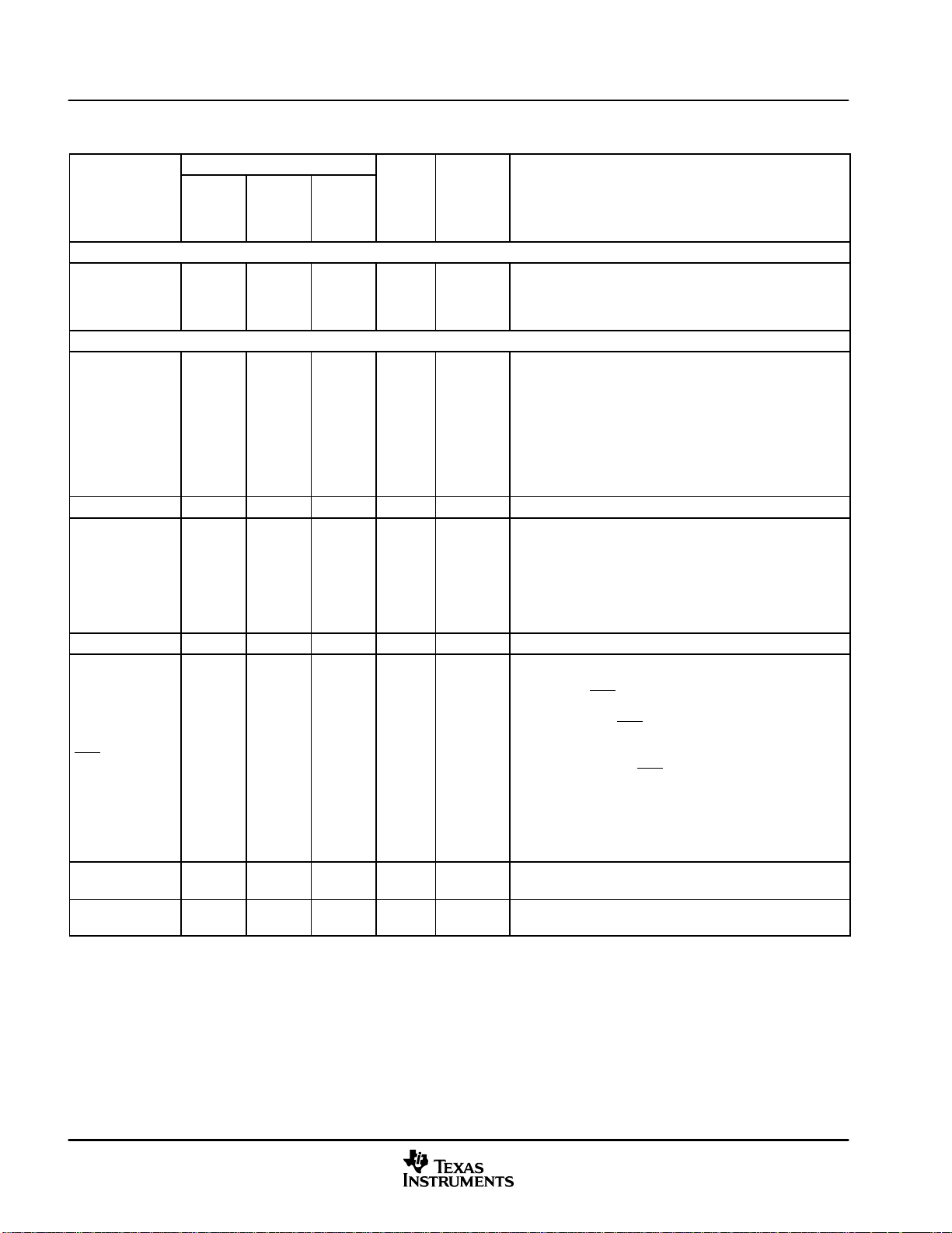
2.3.2 Pin Assignments for the PGF Package
ADVANCE INFORMATION
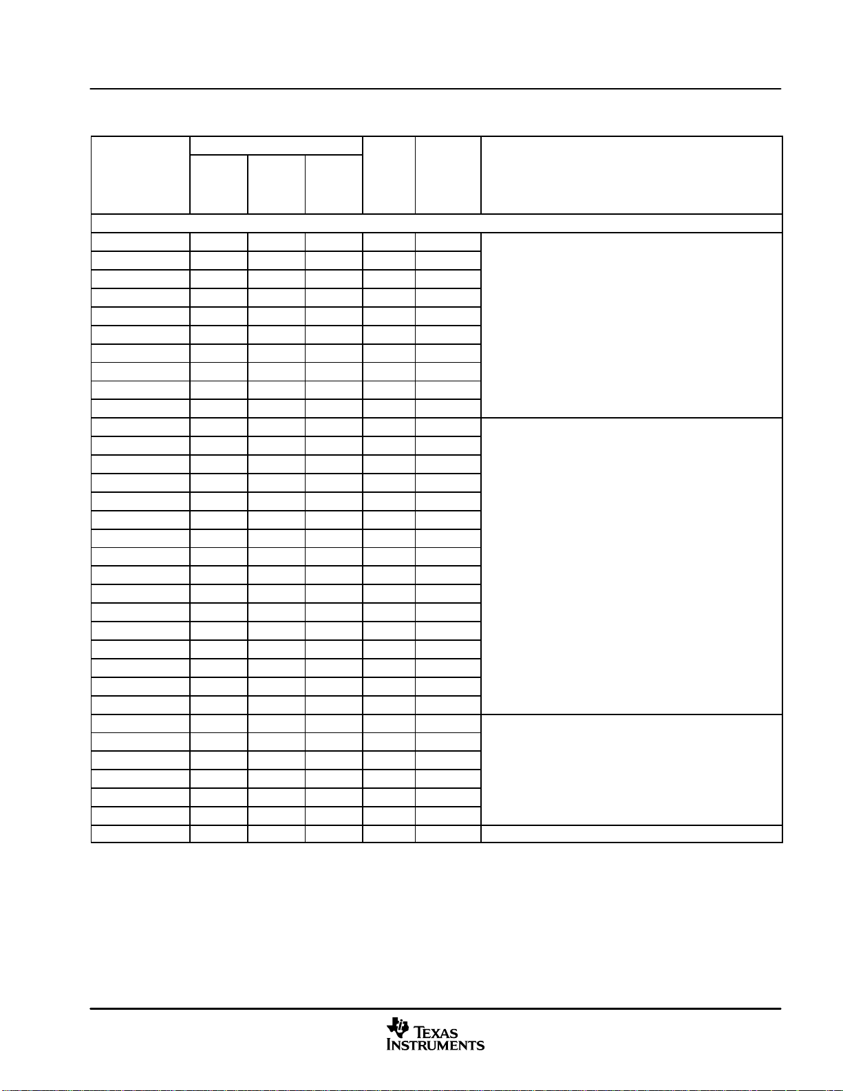
The TMS320R2812 176-pin PGF low-profile quad flatpack (LQFP) pin assignments are shown in Figure 2−2.
See Table 2−2 for a description of each pin’s function(s).
Introduction
XZCS6AND7
TESTSEL
TRST
TCK
EMU0
XA[12]
XD[14]
XF_XPLLDIS
XA[13]
V
V
XA[14]
V
DDIO
EMU1
XD[15]
XA[15]
XINT1_XBIO
XNMI_XINT13
XINT2_ADCSOC
XA[16]
V
V
SCITXDA
XA[17]
SCIRXDA
XA[18]
XHOLD
XRS
XREADY
V
DD1
V
ADCBGREFIN
SS1
V
SSA2
V
DDA2
ADCINA7
ADCINA6
ADCINA5
ADCINA4
ADCINA3
ADCINA2
ADCINA1
ADCINA0
ADCLO
V
SSAIO
SS
VDDV
XA[11]
TDI
XA[10]
TDO
TMS
XA[9]
132 89
133
SS
DD
SS
DD
176
131
130
129
128
127
126
134
135
136
137
138
139
140
141
142
143
144
145
146
147
148
149
150
151
152
153
154
155
156
157
158
159
160
161
162
163
164
165
166
167
168
169
170
171
172
173
174
175
23456789101112131415161718192021222324252627282930313233343536373839404142
125
C2TRIP
C3TRIP
124
123
C1TRIP
XA[8]
121
122
SS
V
XCLKOUT
120
119
XA[7]
TCLKINA
118
117
T2CTRIP / EVASOC
TDIRA
116
115
DDIO
114
T1CTRIP_PDPINTA
VDDVSSV
XA[6]
111
113
112
110
SS
CAP3_QEPI1
XA[5]
CAP2_QEP2
CAP1_QEP1
V
109
108
107
106
105
DD
T2PWM_T2CMP
XA[4]
T1PWM_T1CMP
PWM6
VSSV
99989796959493
101
104
103
102
100
PWM5
XD[13]
XD[12]
PWM4
PWM3
PWM2
PWM1
929190
SCIRXDB
SCITXDB
CANRXA
87
86
85
84
83
82
81
80
79
78
77
76
75
74
73
72
71
70
69
68
67
66
65
64
63
62
61
60
59
58
57
56
55
54
53
52
51
50
49
48
47
46
43
88
XZCS2
CANTXA
V
SS
XA[3]
XWE
T4CTRIP/EVBSOC
XHOLDA
V
DDIO
XA[2]
T3CTRIP_PDPINTB
V
SS
X1/XCLKIN
X2
V
DD
XD[11]
XD[10]
TCLKINB
TDIRB
V
SS
V
DDIO
XD[9]
TEST1
TEST2
XD[8]
V
DDIO
C6TRIP
C5TRIP
C4TRIP
CAP6_QEPI2
CAP5_QEP4
V
SS
CAP4_QEP3
V
DD
T4PWM_T4CMP
XD[7]
T3PWM_T3CMP
V
SS
XR/W
PWM12
PWM11
PWM10
PWM9
PWM8
PWM7
45
1
DDAIO
V
ADCINB0
ADCINB1
ADCINB2
ADCINB3
ADCINB4
ADCINB5
ADCINB6
ADCINB7
ADCREFP
ADCREFM
SSA1
DDA1
V
V
AVSSREFBG
AVDDREFBG
SS
MCXMP/
V
XA[0]
MDRA
ADCRESEXT
XD[0]
MDXA
DD
V
XD[1]
MCLKRA
XD[2]
MFSXA
XD[3]VDDIO
MFSRA
MCLKXA
SS
V
XD[4]
SPICLKA
DD
V
XD[5]
SPISTEA
SS
V
XD[6]
SPISIMOA
XRD
XA[1]
SPISOMIA
44
XZCS0AND1
Figure 2−2. TMS320R2812 176-Pin PGF LQFP (Top View)
June 2004 SPRS257
15
Introduction
ADVANCE INFORMATION
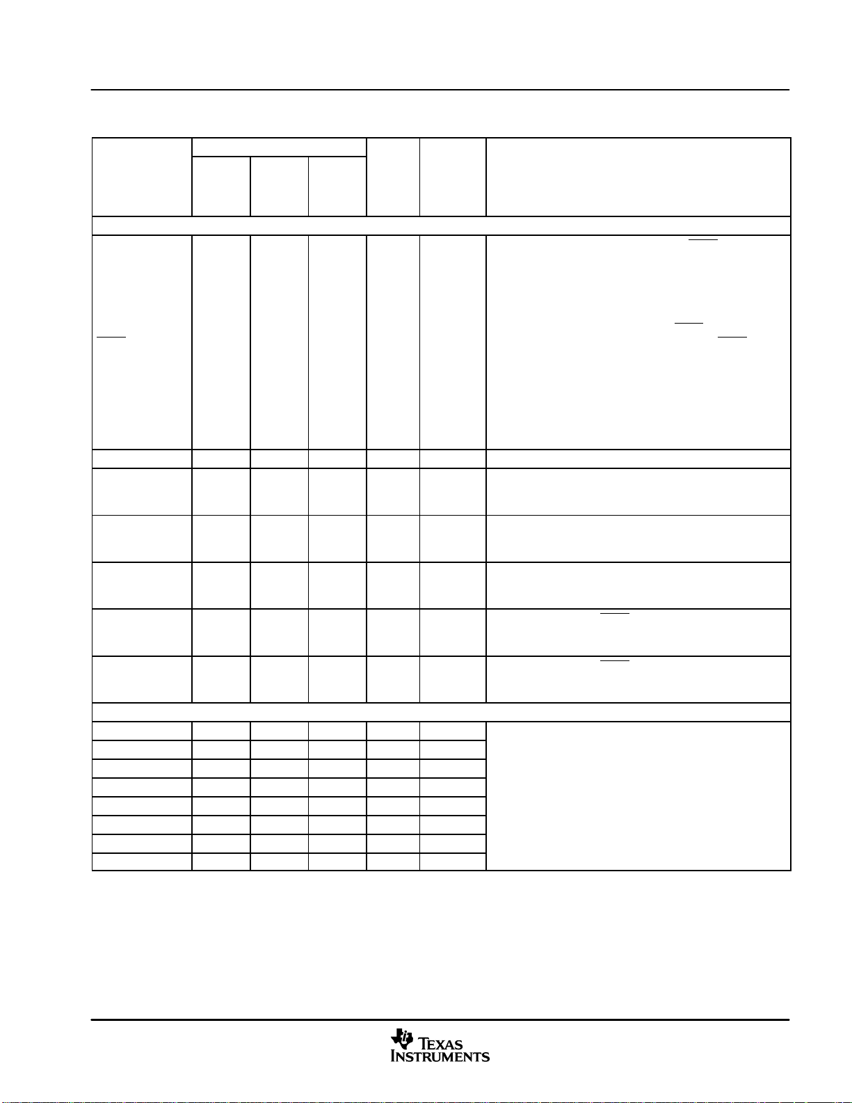
2.3.3 Pin Assignments for the PBK Package
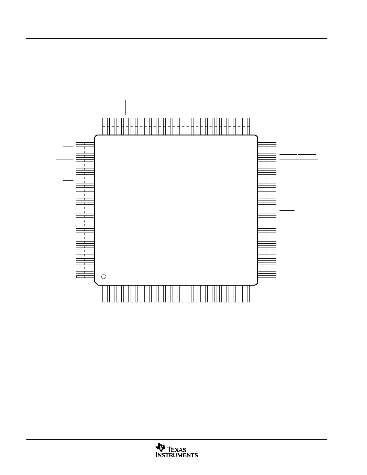
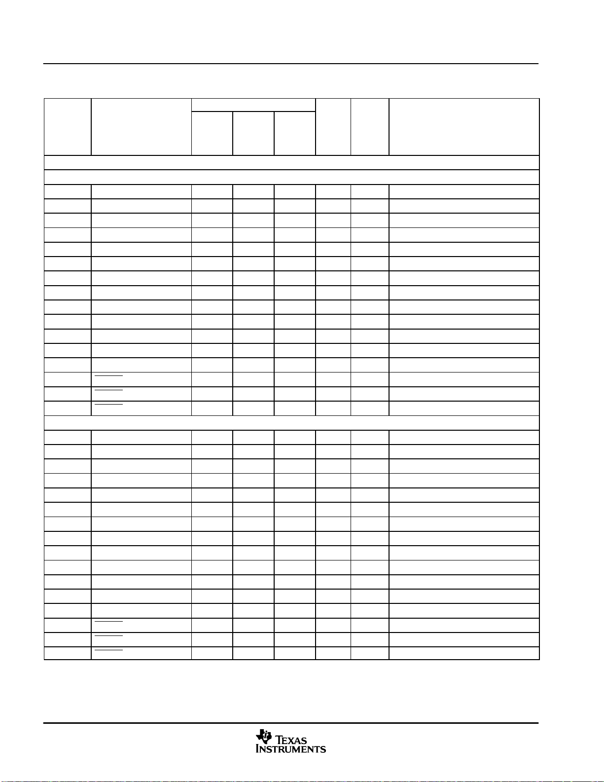
The TMS320R2811 128-pin PBK low-profile quad flatpack (LQFP) pin assignments are shown in Figure 2−3.
See Table 2−2 for a description of each pin’s function(s).
TESTSEL
TRST
TCK
EMU0
XF_XPLLDIS
V
V
V
DDIO
EMU1
XINT1_XBIO
XNMI_XINT13
XINT2_ADCSOC
ADCBGREFIN
V
V
SCITXDA
SCIRXDA
XRS
V
DD1
V
SS1
V
SSA2
V
DDA2
ADCINA7
ADCINA6
ADCINA5
ADCINA4
ADCINA3
ADCINA2
ADCINA1
ADCINA0
ADCLO
V
SSAIO
DD
DD
TCLKINA
TDIRA
T2CTRIP/ EVASOC
84
131415
DDIO
VDDV
83
82
T1CTRIP_PDPINTA
CAP1_QEP1
CAP2_QEP2
CAP3_QEPI1
81
79
78
80
16
18
19
17
DD
T2PWM_T2CMP
T1PWM_T1CMP
76
77
21
20
PWM6
757473
222324
VSSV
PWM5
72
25
PWM4
PWM3
71
70
27
26
PWM1
PWM2
69
68
28
29
SCIRXDB
SCITXDB
CANRXA
66
67
63
62
61
60
59
58
57
56
55
54
53
52
51
50
49
48
47
46
45
44
43
42
41
40
39
38
37
36
35
34
31
30
64
CANTXA
V
DD
V
SS
T4CTRIP
T3CTRIP_PDPINTB
V
SS
X1/XCLKIN
X2
V
DD
TCLKINB
TDIRB
V
SS
V
DDIO
TEST1
TEST2
V
DDIO
C6TRIP
C5TRIP
C4TRIP
CAP6_QEPI2
CAP5_QEP4
CAP4_QEP3
V
DD
T4PWM_T4CMP
T3PWM_T3CMP
V
SS
PWM12
PWM11
PWM10
PWM9
PWM8
PWM7
33
/EVBSOC
SS
TDI
TDO
TMS
VDDV
96 65
97
98
99
100
101
102
SS
SS
128
103
104
105
106
107
108
109
110
111
112
113
114
115
116
117
118
119
120
121
122
123
124
125
126
127
93
9291908988
95
94
2345678
C1TRIP
C2TRIP
C3TRIP
SS
XCLKOUT
V
878685
9
101112
16
1
SS
DD
V
DDAIO
V
ADCINB0
ADCINB1
ADCINB2
ADCINB3
ADCINB4
ADCINB5
ADCINB6
ADCINB7
ADCREFP
ADCREFM
AVSSREFBG
AVDDREFBG
SSA1
DDA1
V
V
ADCRESEXT
MDRA
MDXA
V
MCLKRA
MFSXA
MCLKXA
Figure 2−3. TMS320R2811 128-Pin PBK LQFP
(Top View)
SS
V
DDIO
V
MFSRA
DD
V
V
SPISTEA
SPICLKA
SS
SPISIMOA
SPISOMIA
32
June 2004SPRS257
Introduction
19 bit XINTF Address Bus
ADVANCE INFORMATION
2.4 Signal Descriptions
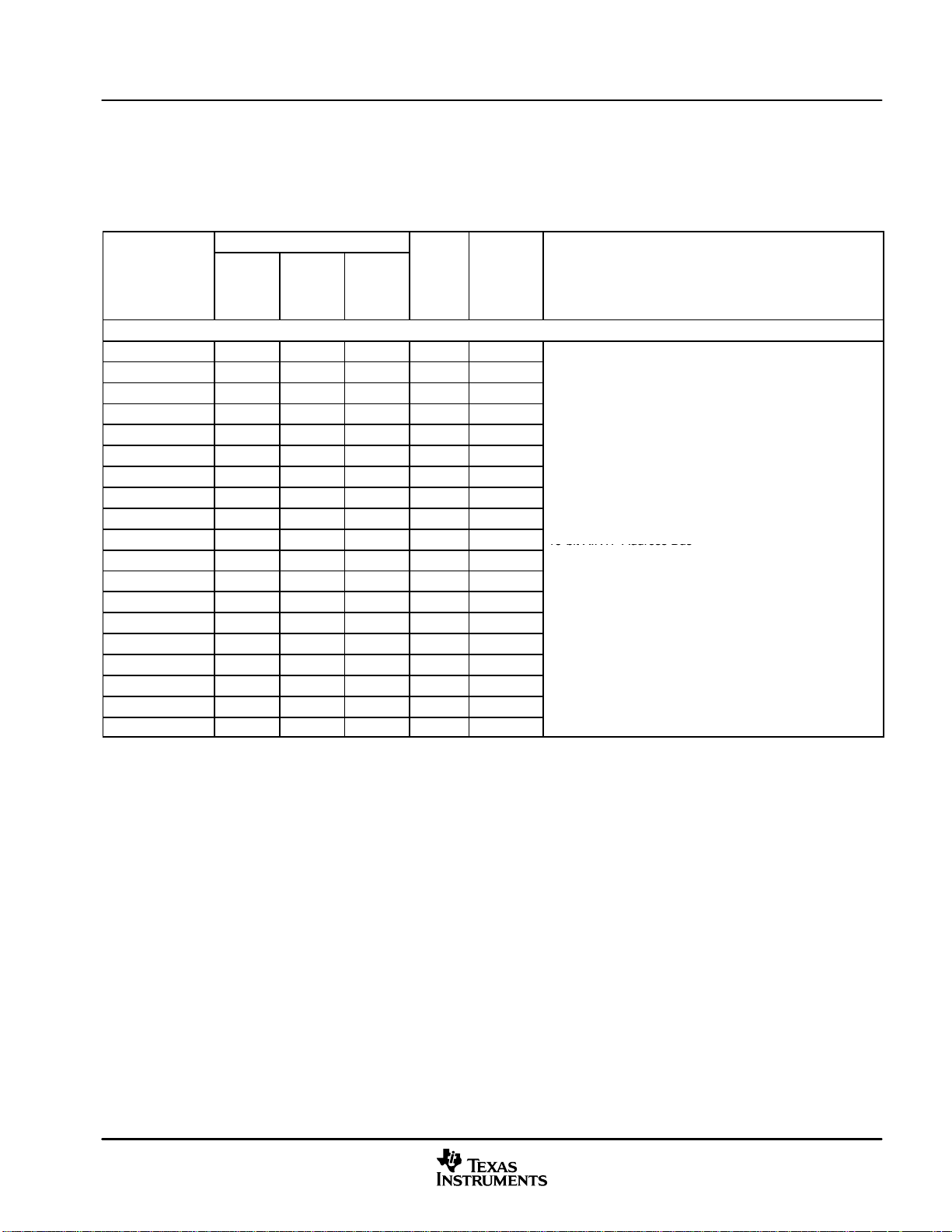
Table 2−2 specifies the signals on the R281x devices. All digital inputs are TTL-compatible. All outputs are
3.3 V with CMOS levels. Inputs are not 5-V tolerant. A 100-µA (or 20-µA) pullup/pulldown is used.
Table 2−2. Signal Descriptions
PIN NO.
NAME
XA[18] D7 158 − O/Z −
XA[17] B7 156 − O/Z −
XA[16] A8 152 − O/Z −
XA[15] B9 148 − O/Z −
XA[14] A10 144 − O/Z −
XA[13] E10 141 − O/Z −
XA[12] C11 138 − O/Z −
XA[11] A14 132 − O/Z
XA[10] C12 130 − O/Z −
XA[9] D14 125 − O/Z −
XA[8] E12 121 − O/Z −
XA[7] F12 118 − O/Z −
XA[6] G14 111 − O/Z −
XA[5] H13 108 − O/Z −
XA[4] J12 103 − O/Z −
XA[3] M11 85 − O/Z −
XA[2] N10 80 − O/Z −
XA[1] M2 43 − O/Z −
XA[0] G5 18 − O/Z
†
Typical drive strength of the output buffer for all pins is 4 mA except for TDO, XCLKOUT, XF, XINTF, EMU0, and EMU1 pins, which are 8 mA.
‡
I = Input, O = Output, Z = High impedance
§
PU = pin has internal pullup; PD = pin has internal pulldown
179-PIN
GHH
AND
ZHH
176-PIN
PGF
128-PIN
PBK
‡
I/O/Z
XINTF SIGNALS (2812 ONLY)
PU/PD
§
19-bit XINTF Address Bus
†
DESCRIPTION
June 2004 SPRS257
17
Introduction
ADVANCE INFORMATION
Table 2−2. Signal Descriptions
PIN NO.
NAME DESCRIPTIONPU/PD
NAME DESCRIPTIONPU/PD
XD[15] A9 147 − I/O/Z PU
XD[14] B11 139 − I/O/Z PU
XD[13] J10 97 − I/O/Z PU
XD[12] L14 96 − I/O/Z PU
XD[11] N9 74 − I/O/Z PU
XD[10] L9 73 − I/O/Z PU
XD[9] M8 68 − I/O/Z PU
XD[8] P7 65 − I/O/Z PU
XD[7] L5 54 − I/O/Z PU
XD[6] L3 39 − I/O/Z PU
XD[5] J5 36 − I/O/Z PU
XD[4] K3 33 − I/O/Z PU
XD[3] J3 30 − I/O/Z PU
XD[2] H5 27 − I/O/Z PU
XD[1] H3 24 − I/O/Z PU
XD[0] G3 21 − I/O/Z PU
†
Typical drive strength of the output buffer for all pins is 4 mA except for TDO, XCLKOUT, XF, XINTF, EMU0, and EMU1 pins, which are 8 mA.
‡
I = Input, O = Output, Z = High impedance
§
PU = pin has internal pullup; PD = pin has internal pulldown
179-PIN
GHH
AND
ZHH
176-PIN
PGF
128-PIN
PBK
I/O/Z
I/O/Z
‡
‡
†
(Continued)
§
§
16-bit XINTF Data Bus
18
June 2004SPRS257
Introduction
ADVANCE INFORMATION
Table 2−2. Signal Descriptions
PIN NO.
NAME DESCRIPTIONPU/PD
NAME DESCRIPTIONPU/PD
XMP/MC F1 17 − I PD
XHOLD E7 159 − I PU
XHOLDA K10 82 − O/Z −
XZCS0AND1 P1 44 − O/Z −
XZCS2 P13 88 − O/Z −
XZCS6AND7 B13 133 − O/Z −
XWE N11 84 − O/Z −
XRD M3 42 − O/Z −
XR/W N4 51 − O/Z −
†
Typical drive strength of the output buffer for all pins is 4 mA except for TDO, XCLKOUT, XF, XINTF, EMU0, and EMU1 pins, which are 8 mA.
‡
I = Input, O = Output, Z = High impedance
§
PU = pin has internal pullup; PD = pin has internal pulldown
179-PIN
GHH
AND
ZHH
176-PIN
PGF
128-PIN
PBK
XINTF SIGNALS (2812 ONLY) (CONTINUED)
I/O/Z
I/O/Z
‡
‡
†
(Continued)
§
§
Microprocessor/Microcomputer Mode Select. Switches
between microprocessor and microcomputer mode. When
high, Zone 7 is enabled on the external interface. When low,
Zone 7 is disabled from the external interface, and on-chip
boot ROM may be accessed instead. This signal is latched
into the XINTCNF2 register on a reset and the user can modify
this bit in software. The state of the XMP/MC
after reset.
External Hold Request. XHOLD, when active (low), requests
the XINTF to release the external bus and place all buses and
strobes into a high-impedance state. The XINTF will release
the bus when any current access is complete and there are no
pending accesses on the XINTF.
External Hold Acknowledge. XHOLDA is driven active (low)
when the XINTF has granted a XHOLD
buses and strobe signals will be in a high-impedance state.
XHOLDA
External devices should only drive the external bus when
XHOLDA
XINTF Zone 0 and Zone 1 Chip Select. XZCS0AND1 is active
(low) when an access to the XINTF Zone 0 or Zone 1 is
performed.
XINTF Zone 2 Chip Select. XZCS2 is active (low) when an
access to the XINTF Zone 2 is performed.
XINTF Zone 6 and Zone 7 Chip Select. XZCS6AND7 is active
(low) when an access to the XINTF Zone 6 or Zone 7 is
performed.
Write Enable. Active-low write strobe. The write strobe
waveform is specified, per zone basis, by the Lead, Active,
and Trail periods in the XTIMINGx registers.
Read Enable. Active-low read strobe. The read strobe
waveform is specified, per zone basis, by the Lead, Active,
and Trail periods in the XTIMINGx registers. NOTE: The XRD
and XWE signals are mutually exclusive.
Read Not Write Strobe. Normally held high. When low, XR/W
indicates write cycle is active; when high, XR/W indicates read
cycle is active.
is released when the XHOLD signal is released.
is active (low).
pin is ignored
request. All XINTF
June 2004 SPRS257
19
Introduction
ADVANCE INFORMATION
Table 2−2. Signal Descriptions
†
(Continued)
PIN NO.
NAME DESCRIPTIONPU/PD
GHH
AND
176-PIN
PGF
128-PIN
PBK
NAME DESCRIPTIONPU/PD
179-PIN
I/O/Z
I/O/Z
‡
‡
§
§
ZHH
XINTF SIGNALS (2812 ONLY) (CONTINUED)
Ready Signal. Indicates peripheral is ready to complete the
XREADY B6 161 − I PU
access when asserted to 1. XREADY can be configured to be
a synchronous or an asynchronous input. See the timing
diagrams for more details.
JTAG AND MISCELLANEOUS SIGNALS
Oscillator Input − input to the internal oscillator. This pin is also
used to feed an external clock. The 28x can be operated with
an external clock source, provided that the proper voltage
levels be driven on the X1/XCLKIN pin. It should be noted that
X1/XCLKIN K9 77 58 I
the X1/XCLKIN pin is referenced to the 1.8-V (or 1.9-V) core
digital power supply (V
(V
). A clamping diode may be used to clamp a buffered
DDIO
), rather than the 3.3-V I/O supply
DD
clock signal to ensure that the logic-high level does not
exceed VDD (1.8 V or 1.9 V) or a 1.8-V oscillator may be used.
X2 M9 76 57 O Oscillator Output
Output clock derived from SYSCLKOUT to be used for
external wait-state generation and as a general-purpose clock
source. XCLKOUT is either the same frequency, 1/2 the
XCLKOUT F11 119 87 O −
frequency, or 1/4 the frequency of SYSCLKOUT. At reset,
XCLKOUT = SYSCLKOUT/4. The XCLKOUT signal can be
turned off by setting bit 3 (CLKOFF) of the XINTCNF2 register
to 1.
TESTSEL A13 134 97 I PD Test Pin. Reserved for TI. Must be connected to ground.
Device Reset (in) and Watchdog Reset (out).
Device reset. XRS causes the device to terminate execution.
The PC will point to the address contained at the location
0x3FFFC0. When XRS
is brought to a high level, execution
begins at the location pointed to by the PC. This pin is driven
XRS D6 160 11 3 I/O PU
low by the DSP when a watchdog reset occurs. During
watchdog reset, the XRS
pin will be driven low for the
watchdog reset duration of 512 XCLKIN cycles.
The output buffer of this pin is an open-drain with an internal
pullup (100 µA, typical). It is recommended that this pin be
driven by an open-drain device.
TEST1 M7 67 51 I/O −
TEST2 N7 66 50 I/O −
†
Typical drive strength of the output buffer for all pins is 4 mA except for TDO, XCLKOUT, XF, XINTF, EMU0, and EMU1 pins, which are 8 mA.
‡
I = Input, O = Output, Z = High impedance
§
PU = pin has internal pullup; PD = pin has internal pulldown
This pin is a “no connect (NC)” (i.e., this pin is not connected
to any circuitry internal to the device).
This pin is a “no connect (NC)” (i.e., this pin is not connected
to any circuitry internal to the device).
20
June 2004SPRS257
Introduction
pins have bee
pins have been fully powered up
ADVANCE INFORMATION
Table 2−2. Signal Descriptions
†
(Continued)
PIN NO.
NAME DESCRIPTIONPU/PD
GHH
AND
176-PIN
PGF
128-PIN
PBK
NAME DESCRIPTIONPU/PD
179-PIN
I/O/Z
I/O/Z
‡
‡
§
§
ZHH
JTAG
JTAG test reset with internal pulldown. TRST, when driven
high, gives the scan system control of the operations of the
device. If this signal is not connected or driven low, the device
operates in its functional mode, and the test reset signals are
ignored.
TRST B12 135 98 I PD
NOTE: Do not use pullup resistors on TRST
pulldown device. In a low-noise environment, TRST
; it has an internal
can be
left floating. In a high-noise environment, an additional
pulldown resistor may be needed. The value of this resistor
should be based on drive strength of the debugger pods
applicable to the design. A 2.2-kΩ resistor generally offers
adequate protection. Since this is application-specific, it is
recommended that each target board is validated for proper
operation of the debugger and the application.
TCK A12 136 99 I PU JTAG test clock with internal pullup
JTAG test-mode select (TMS) with internal pullup. This serial
TMS D13 126 92 I PU
control input is clocked into the TAP controller on the rising
edge of TCK.
JTAG test data input (TDI) with internal pullup. TDI is clocked
TDI C13 131 96 I PU
into the selected register (instruction or data) on a rising edge
of TCK.
JTAG scan out, test data output (TDO). The contents of the
TDO D12 127 93 O/Z −
selected register (instruction or data) is shifted out of TDO on
the falling edge of TCK.
Emulator pin 0. When TRST is driven high, this pin is used
EMU0 D11 137 100 I/O/Z PU
as an interrupt to or from the emulator system and is
defined as input/output through the JTAG scan.
Emulator pin 1. When TRST is driven high, this pin is used
EMU1 C9 146 105 I/O/Z PU
as an interrupt to or from the emulator system and is
defined as input/output through the JTAG scan.
ADC ANALOG INPUT SIGNALS
ADCINA7 B5 167 11 9 I
ADCINA6 D5 168 120 I
ADCINA5 E5 169 121 I
ADCINA4 A4 170 122 I
ADCINA3 B4 171 123 I
8-Channel analog inputs for Sample-and-Hold A. The ADC
pins should not be driven before V
n fully powered up.
.
DDA1
, V
DDA2
, and V
ADCINA2 C4 172 124 I
ADCINA1 D4 173 125 I
ADCINA0 A3 174 126 I
†
Typical drive strength of the output buffer for all pins is 4 mA except for TDO, XCLKOUT, XF, XINTF, EMU0, and EMU1 pins, which are 8 mA.
‡
I = Input, O = Output, Z = High impedance
§
PU = pin has internal pullup; PD = pin has internal pulldown
DDAIO
June 2004 SPRS257
21
Introduction
bee
V
pins have been fully powered up
ADVANCE INFORMATION
Table 2−2. Signal Descriptions
†
(Continued)
PIN NO.
NAME DESCRIPTIONPU/PD
GHH
AND
176-PIN
PGF
128-PIN
PBK
NAME DESCRIPTIONPU/PD
179-PIN
I/O/Z
I/O/Z
‡
‡
§
§
ZHH
ADC ANALOG INPUT SIGNALS (CONTINUED)
ADCINB7 F5 9 9 I
ADCINB6 D1 8 8 I
ADCINB5 D2 7 7 I
ADCINB4 D3 6 6 I
ADCINB3 C1 5 5 I
8-Channel Analog Inputs for Sample-and-Hold B. The ADC
pins should not be driven before the V
V
DDAIO
pins have
n fully powered up.
DDA1
.
, V
DDA2
, and
ADCINB2 B1 4 4 I
ADCINB1 C3 3 3 I
ADCINB0 C2 2 2 I
ADC Voltage Reference Output (2 V). Requires a low ESR
(50 mΩ − 1.5 Ω) ceramic bypass capacitor of 10 µF to analog
ADCREFP E2 11 11 I/O
ground. (Can accept external reference input (2 V) if the
software bit is enabled for this mode. 1−10 µF low ESR
capacitor can be used in the external reference mode.)
ADC Voltage Reference Output (1 V). Requires a low ESR
(50 mΩ − 1.5 Ω) ceramic bypass capacitor of 10 µF to analog
ADCREFM E4 10 10 I/O
ground. (Can accept external reference input (1 V) if the
software bit is enabled for this mode. 1−10 µF low ESR
capacitor can be used in the external reference mode.)
ADCRESEXT F2 16 16 O ADC External Current Bias Resistor (24.9 kΩ ±5%)
ADCBGREFIN E6 164 11 6 I Test Pin. Reserved for TI. Must be left unconnected.
AVSSREFBG E3 12 12 I ADC Analog GND
AVDDREFBG E1 13 13 I ADC Analog Power (3.3-V)
ADCLO B3 175 127 I Common Low Side Analog Input. Connect to analog ground.
V
SSA1
V
SSA2
V
DDA1
V
DDA2
V
SS1
V
DD1
V
DDAIO
V
SSAIO
†
Typical drive strength of the output buffer for all pins is 4 mA except for TDO, XCLKOUT, XF, XINTF, EMU0, and EMU1 pins, which are 8 mA.
‡
I = Input, O = Output, Z = High impedance
§
PU = pin has internal pullup; PD = pin has internal pulldown
F3 15 15 I ADC Analog GND
C5 165 117 I ADC Analog GND
F4 14 14 I ADC Analog 3.3-V Supply
A5 166 118 I ADC Analog 3.3-V Supply
C6 163 115 I ADC Digital GND
A6 162 114 I ADC Digital 1.8-V (or 1.9-V) Supply
B2 1 1 3.3-V Analog I/O Power Pin
A2 176 128 Analog I/O Ground Pin
22
June 2004SPRS257
Introduction
equirements
requirements
ADVANCE INFORMATION
Table 2−2. Signal Descriptions
†
(Continued)
PIN NO.
NAME DESCRIPTIONPU/PD
GHH
AND
176-PIN
PGF
128-PIN
PBK
NAME DESCRIPTIONPU/PD
179-PIN
I/O/Z
I/O/Z
‡
‡
§
§
ZHH
POWER SIGNALS
V
DD
V
DD
V
DD
V
DD
V
DD
V
DD
V
DD
V
DD
V
DD
V
DD
V
SS
V
SS
V
SS
V
SS
V
SS
V
SS
V
SS
V
SS
V
SS
V
SS
V
SS
V
SS
V
SS
V
SS
V
SS
V
SS
V
DDIO
V
DDIO
V
DDIO
V
DDIO
V
DDIO
V
DDIO
V
DDIO
†
Typical drive strength of the output buffer for all pins is 4 mA except for TDO, XCLKOUT, XF, XINTF, EMU0, and EMU1 pins, which are 8 mA.
‡
I = Input, O = Output, Z = High impedance
§
PU = pin has internal pullup; PD = pin has internal pulldown
H1 23 20
L1 37 29
P5 56 42
P9 75 56
P12 − 63
K12 100 74
G12 11 2 82
C14 128 94
B10 143 102
C8 154 110
G4 19 17
K1 32 26
L2 38 30
P4 52 39
K6 58 −
P8 70 53
M10 78 59
L11 86 62
K13 99 73
J14 105 −
G13 11 3 −
E14 120 88
B14 129 95
D10 142 −
C10 − 103
B8 153 109
J4 31 25
L7 64 49
L10 81 −
N14 − −
G11 114 83
E9 145 104
N8 69 52
1.8-V or 1.9-V Core Digital Power Pins. See Section 6.2,
Recommended Operating Conditions, for voltage
.
r
.
Core and Digital I/O Ground Pins
3.3-V I/O Digital Power Pins
June 2004 SPRS257
23
Introduction
ADVANCE INFORMATION
Table 2−2. Signal Descriptions† (Continued)
PIN NO.
GPIO PERIPHERAL SIGNAL
GPIOA0 PWM1 (O) M12 92 68 I/O/Z PU GPIO or PWM Output Pin #1
GPIOA1 PWM2 (O) M14 93 69 I/O/Z PU GPIO or PWM Output Pin #2
GPIOA2 PWM3 (O) L12 94 70 I/O/Z PU GPIO or PWM Output Pin #3
GPIOA3 PWM4 (O) L13 95 71 I/O/Z PU GPIO or PWM Output Pin #4
GPIOA4 PWM5 (O) K11 98 72 I/O/Z PU GPIO or PWM Output Pin #5
GPIOA5 PWM6 (O) K14 101 75 I/O/Z PU GPIO or PWM Output Pin #6
GPIOA6 T1PWM_T1CMP (I) J11 102 76 I/O/Z PU GPIO or Timer 1 Output
GPIOA7 T2PWM_T2CMP (I) J13 104 77 I/O/Z PU GPIO or Timer 2 Output
GPIOA8 CAP1_QEP1 (I) H10 106 78 I/O/Z PU GPIO or Capture Input #1
GPIOA9 CAP2_QEP2 (I) H11 107 79 I/O/Z PU GPIO or Capture Input #2
GPIOA10 CAP3_QEPI1 (I) H12 109 80 I/O/Z PU GPIO or Capture Input #3
GPIOA11 TDIRA (I) F14 116 85 I/O/Z PU GPIO or Timer Direction
GPIOA12 TCLKINA (I) F13 117 86 I/O/Z PU GPIO or Timer Clock Input
GPIOA13 C1TRIP (I) E13 122 89 I/O/Z PU GPIO or Compare 1 Output Trip
GPIOA14 C2TRIP (I) E11 123 90 I/O/Z PU GPIO or Compare 2 Output Trip
GPIOA15 C3TRIP (I) F10 124 91 I/O/Z PU GPIO or Compare 3 Output Trip
GPIOB0 PWM7 (O) N2 45 33 I/O/Z PU GPIO or PWM Output Pin #7
GPIOB1 PWM8 (O) P2 46 34 I/O/Z PU GPIO or PWM Output Pin #8
GPIOB2 PWM9 (O) N3 47 35 I/O/Z PU GPIO or PWM Output Pin #9
GPIOB3 PWM10 (O) P3 48 36 I/O/Z PU GPIO or PWM Output Pin #10
GPIOB4 PWM11 (O) L4 49 37 I/O/Z PU GPIO or PWM Output Pin #11
GPIOB5 PWM12 (O) M4 50 38 I/O/Z PU GPIO or PWM Output Pin #12
GPIOB6 T3PWM_T3CMP (I) K5 53 40 I/O/Z PU GPIO or Timer 3 Output
GPIOB7 T4PWM_T4CMP (I) N5 55 41 I/O/Z PU GPIO or Timer 4 Output
GPIOB8 CAP4_QEP3 (I) M5 57 43 I/O/Z PU GPIO or Capture Input #4
GPIOB9 CAP5_QEP4 (I) M6 59 44 I/O/Z PU GPIO or Capture Input #5
GPIOB10 CAP6_QEPI2 (I) P6 60 45 I/O/Z PU GPIO or Capture Input #6
GPIOB11 TDIRB (I) L8 71 54 I/O/Z PU GPIO or Timer Direction
GPIOB12 TCLKINB (I) K8 72 55 I/O/Z PU GPIO or Timer Clock Input
GPIOB13 C4TRIP (I) N6 61 46 I/O/Z PU GPIO or Compare 4 Output Trip
GPIOB14 C5TRIP (I) L6 62 47 I/O/Z PU GPIO or Compare 5 Output Trip
GPIOB15 C6TRIP (I) K7 63 48 I/O/Z PU GPIO or Compare 6 Output Trip
179-PIN
GHH
AND
ZHH
176-PIN
PGF
GPIO OR PERIPHERAL SIGNALS
GPIOA OR EVA SIGNALS
GPIOB OR EVB SIGNALS
128-PIN
PBK
I/O/Z‡PU/PD
§
DESCRIPTION
†
Typical drive strength of the output buffer for all pins [except TDO, XCLKOUT, XF, XINTF, EMU0, and EMU1 pins] is 4 mA typical.
‡
I = Input, O = Output, Z = High impedance
§
PU = pin has internal pullup; PD = pin has internal pulldown
24
June 2004SPRS257
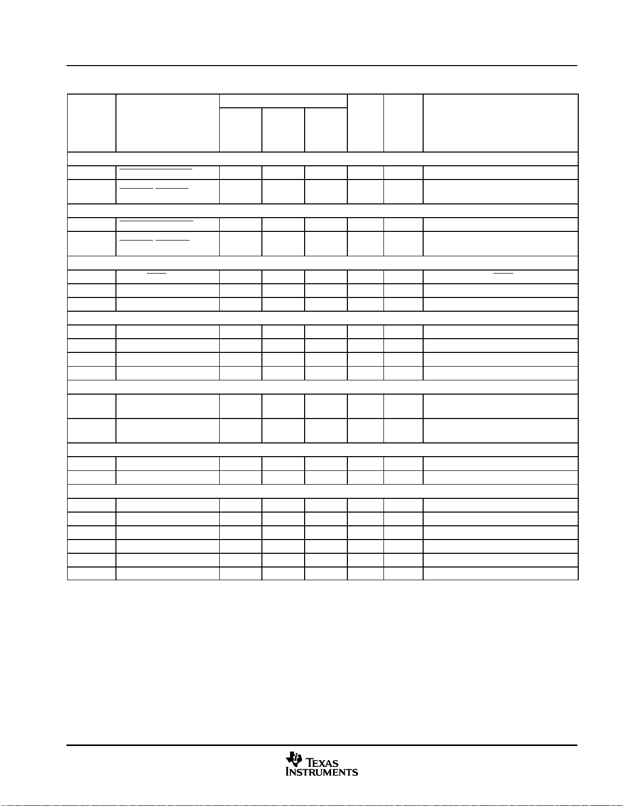
ADVANCE INFORMATION
Introduction
Table 2−2. Signal Descriptions† (Continued)
PIN NO.
GPIO PERIPHERAL SIGNAL
GPIOD0 T1CTRIP_PDPINTA (I) H14 110 81 I/O/Z PU Timer 1 Compare Output Trip
GPIOD1 T2CTRIP/EVASOC (I) G10 115 84 I/O/Z PU
GPIOD5 T3CTRIP_PDPINTB (I) P10 79 60 I/O/Z PU Timer 3 Compare Output Trip
GPIOD6 T4CTRIP/EVBSOC (I) P11 83 61 I/O/Z PU
GPIOE0 XINT1_XBIO (I) D9 149 106 I/O/Z − GPIO or XINT1 or XBIO input
GPIOE1 XINT2_ADCSOC (I) D8 151 108 I/O/Z − GPIO or XINT2 or ADC start of conversion
GPIOE2 XNMI_XINT13 (I) E8 150 107 I/O/Z PU GPIO or XNMI or XINT13
GPIOF0 SPISIMOA (O) M1 40 31 I/O/Z − GPIO or SPI slave in, master out
GPIOF1 SPISOMIA (I) N1 41 32 I/O/Z − GPIO or SPI slave out, master in
GPIOF2 SPICLKA (I/O) K2 34 27 I/O/Z − GPIO or SPI clock
GPIOF3 SPISTEA (I/O) K4 35 28 I/O/Z − GPIO or SPI slave transmit enable
GPIOF4 SCITXDA (O) C7 155 111 I/O/Z PU
GPIOF5 SCIRXDA (I) A7 157 11 2 I/O/Z PU
GPIOF6 CANTXA (O) N12 87 64 I/O/Z PU GPIO or eCAN transmit data
GPIOF7 CANRXA (I) N13 89 65 I/O/Z PU GPIO or eCAN receive data
GPIOF8 MCLKXA (I/O) J1 28 23 I/O/Z PU GPIO or transmit clock
GPIOF9 MCLKRA (I/O) H2 25 21 I/O/Z PU GPIO or receive clock
GPIOF10 MFSXA (I/O) H4 26 22 I/O/Z PU GPIO or transmit frame synch
GPIOF11 MFSRA (I/O) J2 29 24 I/O/Z PU GPIO or receive frame synch
GPIOF12 MDXA (O) G1 22 19 I/O/Z − GPIO or transmitted serial data
GPIOF13 MDRA (I) G2 20 18 I/O/Z PU GPIO or received serial data
†
Typical drive strength of the output buffer for all pins [except TDO, XCLKOUT, XF, XINTF, EMU0, and EMU1 pins] is 4 mA typical.
‡
I = Input, O = Output, Z = High impedance
§
PU = pin has internal pullup; PD = pin has internal pulldown
179-PIN
GHH
AND
ZHH
176-PIN
PGF
GPIOD OR EVA SIGNALS
GPIOD OR EVB SIGNALS
GPIOE OR INTERRUPT SIGNALS
GPIOF OR SPI SIGNALS
GPIOF OR SCI-A SIGNALS
GPIOF OR CAN SIGNALS
GPIOF OR McBSP SIGNALS
128-PIN
PBK
I/O/Z‡PU/PD
§
Timer 2 Compare Output Trip or External
ADC Start-of-Conversion EV-A
Timer 4 Compare Output Trip or External
ADC Start-of-Conversion EV-B
GPIO or SCI asynchronous serial port TX
data
GPIO or SCI asynchronous serial port RX
data
DESCRIPTION
June 2004 SPRS257
25
Introduction
ADVANCE INFORMATION
Table 2−2. Signal Descriptions† (Continued)
PIN NO.
GPIO PERIPHERAL SIGNAL
GPIOF14 XF_XPLLDIS (O) A11 140 101 I/O/Z PU
GPIOG4 SCITXDB (O) P14 90 66 I/O/Z −
GPIOG5 SCIRXDB (I) M13 91 67 I/O/Z −
†
Typical drive strength of the output buffer for all pins [except TDO, XCLKOUT, XF, XINTF, EMU0, and EMU1 pins] is 4 mA typical.
‡
I = Input, O = Output, Z = High impedance
§
PU = pin has internal pullup; PD = pin has internal pulldown
179-PIN
GHH
AND
ZHH
176-PIN
PGF
GPIOF OR XF CPU OUTPUT SIGNAL
GPIOG OR SCI-B SIGNALS
128-PIN
PBK
I/O/Z‡PU/PD
§
This pin has three functions:
1. XF − General-purpose output pin.
2. XPLLDIS − This pin will be sampled
during reset to check if the PLL needs
to be disabled. The PLL will be
disabled if this pin is sensed low. HALT
and STANDBY modes cannot be used
when the PLL is disabled.
3. GPIO − GPIO function
GPIO or SCI asynchronous serial port
transmit data
GPIO or SCI asynchronous serial port
receive data
DESCRIPTION
NOTE:
Other than the power supply pins, no pin should be driven before the 3.3-V rail has reached
recommended operating conditions. However, it is acceptable for an I/O pin to ramp along with
the 3.3-V supply.
26
June 2004SPRS257
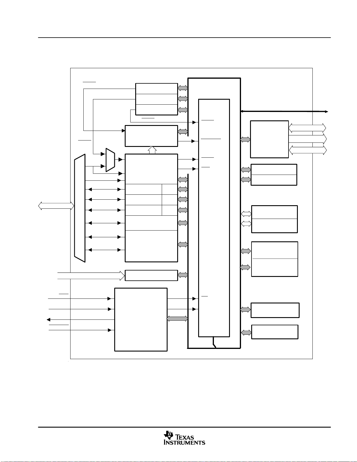
3 Functional Overview
ADVANCE INFORMATION
Functional Overview
Memory Bus
GPIO Pins
TINT0
TINT1
G
P
I
O
M
U
X
XINT13
XNMI
CPU-Timer 0
CPU-Timer 1
CPU-Timer 2
TINT2
PIE
(96 interrupts)
External Interrupt
Control
(XINT1/2/13, XNMI)
SCIA/SCIB
SPI FIFO
McBSP
eCAN
EVA/EVB
†
FIFO
FIFO
INT14
INT[12:1]
INT13
NMI
C28x CPU
Real-Time JTAG
External
Interface
‡
(XINTF)
M0 SARAM
1K x 16
M1 SARAM
1K x 16
L0 SARAM
4K x 16
L1 SARAM
4K x 16
L2 SARAM
1K X 16
Control
Address(19)
Data(16)
XRS
X1/XCLKIN
X2
XF_XPLLDIS
†
45 of the possible 96 interrupts are used on the devices.
‡
XINTF is available on the R2812 devices only.
16 Channels
12-Bit ADC
System Control
(Oscillator and PLL
+
Peripheral Clocking
+
Low-Power
Modes
+
WatchDog)
Peripheral Bus
RS
CLKIN
Memory Bus
Figure 3−1. Functional Block Diagram
L3 SARAM
1K X 16
H0 SARAM
8K × 16
Boot ROM
4K × 16
June 2004 SPRS257
27
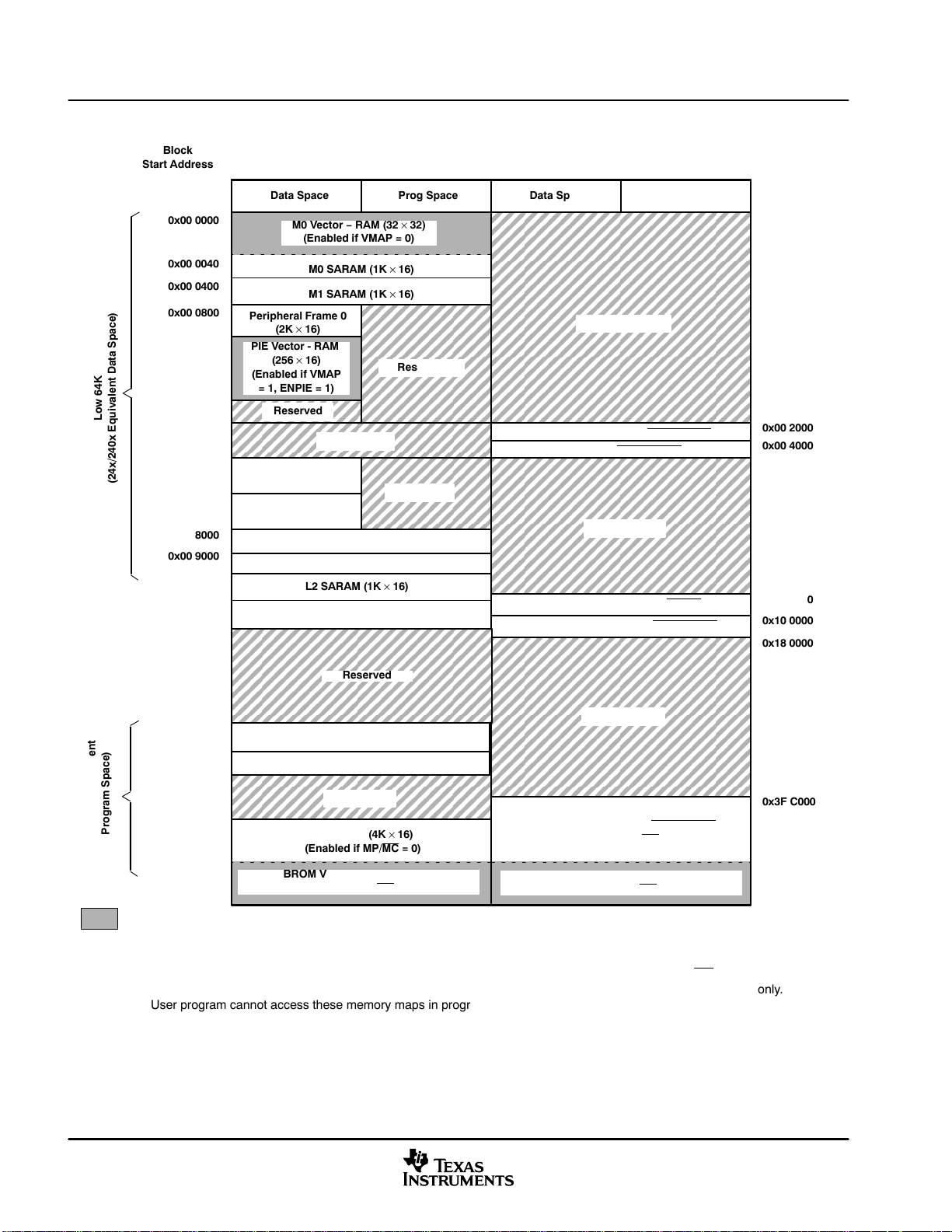
Functional Overview
ADVANCE INFORMATION
3.1 Memory Map
Block
Start Address
On-Chip Memory External Memory XINTF
0x00 0000
0x00 0040
0x00 0400
0x00 0800
0x00 0D00
Low 64K
(24x/240x Equivalent Data Space)
0x00 0E00
0x00 2000
0x00 6000
0x00 7000
0x00 8000
0x00 9000
0x00 A000
0x00 A400
0x00 A800
Data Space Prog Space
M0 Vector − RAM (32 × 32)
(Enabled if VMAP = 0)
M0 SARAM (1K × 16)
M1 SARAM (1K × 16)
Peripheral Frame 0
(2K × 16)
PIE Vector - RAM
(256 × 16)
(Enabled if VMAP
= 1, ENPIE = 1)
Reserved
Reserved
Peripheral Frame 1
(4K × 16, Protected)
Peripheral Frame 2
(4K × 16, Protected)
L0 SARAM (4K × 16)
L1 SARAM (4K × 16)
L2 SARAM (1K × 16)
L3 SARAM (1K × 16)
Reserved
Reserved
Data Space Prog Space
Reserved
XINTF Zone 0 (8K × 16, XZCS0AND1
XINTF Zone 1 (8K × 16, XZCS0AND1) (Protected)
Reserved
XINTF Zone 2 (0.5M × 16, XZCS2
XINTF Zone 6 (0.5M × 16, XZCS6AND7)
)
)
0x00 2000
0x00 4000
0x08 0000
0x10 0000
0x18 0000
NOTES: A. Memory blocks are not to scale.
High 64K
Program Space)
(24x/240x Equivalent
LEGEND:
Only one of these vector maps—M0 vector, PIE vector, BROM vector, XINTF vector—should be enabled at a time.
B. Reserved locations are reserved for future expansion. Application should not access these areas.
C. Boot ROM and Zone 7 memory maps are active either in on-chip or XINTF zone depending on MP/MC, not in both.
D. Peripheral Frame 0, Peripheral Frame 1, and Peripheral Frame 2 memory maps are restricted to data memory only.
User program cannot access these memory maps in program space.
E. “Protected” means the order of Write followed by Read operations is preserved rather than the pipeline order.
F. Certain memory ranges are EALLOW protected against spurious writes after configuration.
G. Zones 0 and 1 and Zones 6 and 7 share the same chip select; hence, these memory blocks have mirrored locations.
H. The passwords are set to all ones.
0x3F7FF8
0x3F 8000
0x3F A000
0x3F F000
0x3F FFC0
Reserved
Reserved
128-bit Password (see Note H)
H0 SARAM (8K × 16)
Reserved
Boot ROM (4K × 16)
(Enabled if MP/MC
BROM Vector - ROM (32 × 32)
(Enabled if VMAP = 1, MP/MC
= 0)
= 0, ENPIE = 0)
XINTF Zone 7 (16K × 16, XZCS6AND7
(Enabled if MP/MC
XINTF Vector - RAM (32 × 32)
(Enabled if VMAP = 1, MP/MC
Figure 3−2. R2812 Memory Map (See Notes A through H)
0x3F C000
)
= 1)
= 1, ENPIE = 0)
28
June 2004SPRS257
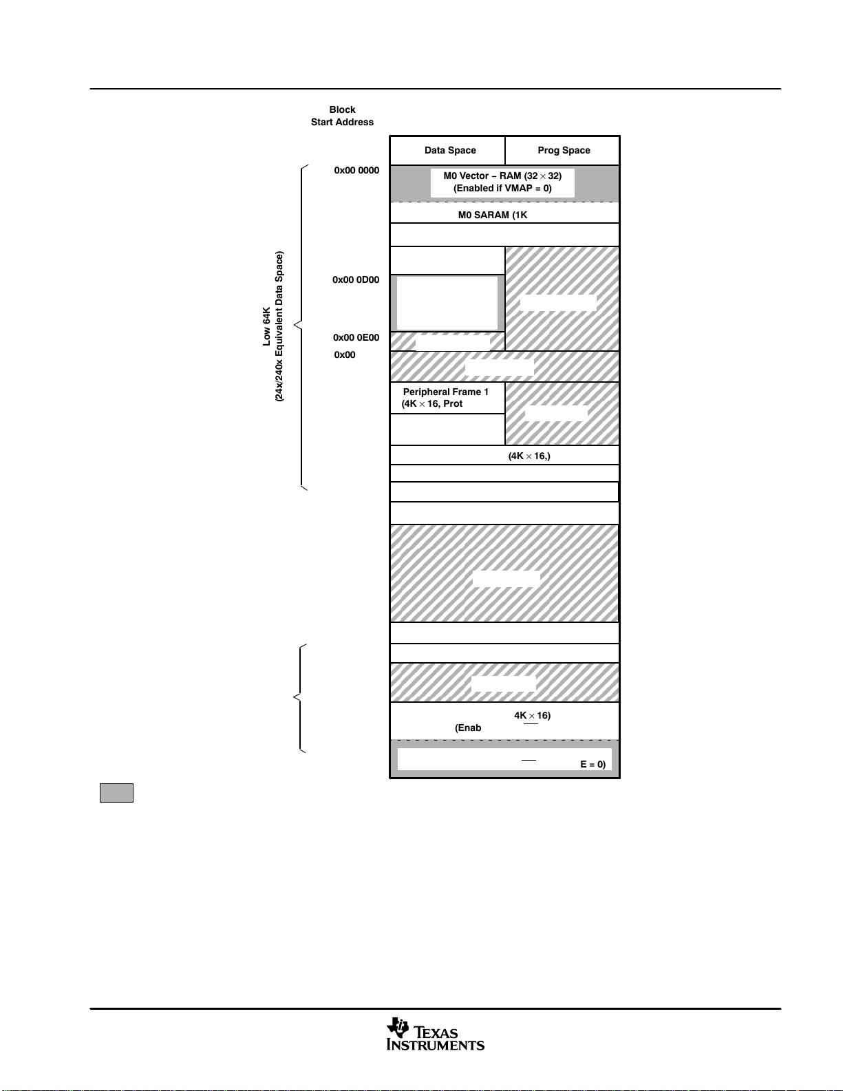
Functional Overview
ADVANCE INFORMATION
Block
Start Address
0x00 0000
0x00 0040
0x00 0400
0x00 0800
0x00 0D00
Low 64K
(24x/240x Equivalent Data Space)
0x00 0E00
0x00 2000
0x00 6000
0x00 7000
0x00 8000
0x00 9000
0x00 A000
0x00 A400
0x00 A800
On-Chip Memory
Data Space Prog Space
M0 Vector − RAM (32 × 32)
(Enabled if VMAP = 0)
M0 SARAM (1K × 16)
M1 SARAM (1K × 16)
Peripheral Frame 0
(2K × 16)
PIE Vector - RAM
(256 × 16)
(Enabled if VMAP
= 1, ENPIE = 1)
Reserved
Reserved
Peripheral Frame 1
(4K × 16, Protected)
Peripheral Frame 2
(4K × 16, Protected)
L0 SARAM (4K × 16,)
L1 SARAM (4K × 16)
L2 SARAM (1K × 16)
L3 SARAM (1K × 16)
Reserved
Reserved
High 64K
Program Space)
(24x/240x Equivalent
LEGEND:
Only one of these vector maps—M0 vector, PIE vector, BROM vector, XINTF vector—should be enabled at a time.
NOTES: A. Memory blocks are not to scale.
B. Reserved locations are reserved for future expansion. Application should not access these areas.
C. Peripheral Frame 0, Peripheral Frame 1, and Peripheral Frame 2 memory maps are restricted to data memory only. User program
cannot access these memory maps in program space.
D. “Protected” means the order of Write followed by Read operations is preserved rather than the pipeline order.
E. Certain memory ranges are EALLOW protected against spurious writes after configuration.
F. The passwords are set to all ones.
Figure 3−3. R2811 Memory Map (See Notes A through F)
0x3F 7FF8
0x3F 8000
0x3F A000
0x3F F000
0x3F FFC0
Reserved
128-bit Password (see Note F)
H0 SARAM (8K × 16)
Reserved
Boot ROM (4K × 16)
(Enabled if MP/MC
BROM Vector - ROM (32 × 32)
(Enabled if VMAP = 1, MP/MC
= 0)
= 0, ENPIE = 0)
June 2004 SPRS257
29

Functional Overview
ADVANCE INFORMATION
The low 64K of the memory-address range maps into the data space of the 240x. The “High 64K” of the
memory address range maps into the program space of the 24x/240x. 24x/240x-compatible code will only
execute from the “High 64K” memory area. Hence, the top 32K of H0 SARAM block can be used to run
24x/240x-compatible code (if MP/MC
(if MP/MC
The XINTF consists of five independent zones. One zone has its own chip select and the remaining four zones
share two chip selects. Each zone can be programmed with its own timing (wait states) and to either sample
or ignore external ready signal. This makes interfacing to external peripherals easy and glueless.
The chip selects of XINTF Zone 0 and Zone 1 are merged together into a single chip select
(XZCS0AND1
a single chip select (XZCS6AND7
for details.
Peripheral Frame 1, Peripheral Frame 2, and XINTF Zone 1 are grouped together so as to enable these blocks
to be “write/read peripheral block protected”. The “protected” mode ensures that all accesses to these blocks
happen as written. Because of the C28x pipeline, a write immediately followed by a read, to different memory
locations, will appear in reverse order on the memory bus of the CPU. This can cause problems in certain
peripheral applications where the user expected the write to occur first (as written). The C28x CPU supports
a block protection mode where a region of memory can be protected so as to make sure that operations occur
as written (the penalty is extra cycles are added to align the operations). This mode is programmable and by
default, it will protect the selected zones.
mode is low) or, on the 2812, code can be executed from XINTF Zone 7
mode is high).
NOTE:
); and the chip selects of XINTF Zone 6 and Zone 7 are merged together into
). See Section 3.5, “External Interface, XINTF (2812 only)”,
On the 2812, at reset, XINTF Zone 7 is accessed if the XMP/MC
microprocessor or microcomputer mode of operation. In microprocessor mode, Zone 7 is mapped to high
memory such that the vector table is fetched externally. The Boot ROM is disabled in this mode. In
microcomputer mode, Zone 7 is disabled such that the vectors are fetched from Boot ROM. This allows the
user to either boot from on-chip memory or from off-chip memory. The state of the XMP/MC
is stored in an MP/MC
hence control the mapping of Boot ROM and XINTF Zone 7. No other memory blocks are affected by
XMP/MC
I/O space is not supported on the 2812 XINTF.
The wait states for the various spaces in the memory map area are listed in Table 3−1.
.
mode bit in the XINTCNF2 register. The user can change this mode in software and
pin is pulled high. This signal selects
signal on reset
30
June 2004SPRS257

AREA WAIT-STATES COMMENTS
ADVANCE INFORMATION
M0 and M1 SARAMs 0-wait Fixed
Peripheral Frame 0 0-wait Fixed
Peripheral Frame 1
Peripheral Frame 2
L0, L1, L2, and L3 SARAMs 0-wait
H0 SARAM 0-wait Fixed
Boot-ROM 1-wait Fixed
XINTF
0-wait (writes)
2-wait (reads)
0-wait (writes)
2-wait (reads)
Programmable,
1-wait minimum
3.2 Brief Descriptions
3.2.1 C28x CPU
The C28x DSP generation is the newest member of the TMS320C2000 DSP platform. The C28x is source
code compatible to the 24x/240x DSP devices, hence existing 240x users can leverage their significant
software investment. Additionally, the C28x is a very efficient C/C++ engine, hence enabling users to develop
not only their system control software in a high-level language, but also enables math algorithms to be
developed using C/C++. The C28x is as efficient in DSP math tasks as it is in system control tasks that typically
are handled by microcontroller devices. This efficiency removes the need for a second processor in many
systems. The 32 x 32-bit MAC capabilities of the C28x and its 64-bit processing capabilities, enable the C28x
to efficiently handle higher numerical resolution problems that would otherwise demand a more expensive
floating-point processor solution. Add to this the fast interrupt response with automatic context save of critical
registers, resulting in a device that is capable of servicing many asynchronous events with minimal latency.
The C28x has an 8-level-deep protected pipeline with pipelined memory accesses. This pipelining enables
the C28x to execute at high speeds without resorting to expensive high-speed memories. Special
branch-look-ahead hardware minimizes the latency for conditional discontinuities. Special store conditional
operations further improve performance.
Functional Overview
Table 3−1. Wait States
Fixed
Fixed
Programmed via the XINTF registers.
Cycles can be extended by external memory or peripheral.
0-wait operation is not possible.
3.2.2 Memory Bus (Harvard Bus Architecture)
As with many DSP type devices, multiple busses are used to move data between the memories and
peripherals and the CPU. The R28x memory bus architecture contains a program read bus, data read bus
and data write bus. The program read bus consists of 22 address lines and 32 data lines. The data read and
write busses consist of 32 address lines and 32 data lines each. The 32-bit-wide data busses enable single
cycle 32-bit operations. The multiple-bus architecture, commonly termed “Harvard Bus”, enables the R28x
to fetch an instruction, read a data value, and write a data value in a single cycle. All peripherals and memories
attached to the memory bus prioritize memory accesses.
C28x and TMS320C2000 are trademarks of Texas Instruments.
June 2004 SPRS257
31

Functional Overview
ADVANCE INFORMATION
Generally, the priority of memory bus accesses can be summarized as follows:
Highest: Data Writes (Simultaneous data and program writes cannot occur
on the memory bus.)
Program Writes (Simultaneous data and program writes cannot occur
on the memory bus.)
Data Reads
Program Reads (Simultaneous program reads and fetches cannot occur
Lowest: Fetches (Simultaneous program reads and fetches cannot occur
3.2.3 Peripheral Bus
To enable migration of peripherals between various Texas Instruments (TI) DSP family of devices, R281x
adopts a peripheral bus standard for peripheral interconnect. The peripheral bus bridge multiplexes the
various busses that make up the processor “Memory Bus” into a single bus consisting of 16 address lines and
16 or 32 data lines and associated control signals. Two versions of the peripheral bus are supported on R281x.
One version only supports 16-bit accesses (called peripheral frame 2) and this retains compatibility with
C240x-compatible peripherals. The other version supports both 16- and 32-bit accesses (called peripheral
frame 1).
3.2.4 Real-Time JTAG and Analysis
on the memory bus.)
on the memory bus.)
3.2.5 External Interface (XINTF) (2812 Only)
3.2.6 M0, M1 SARAMs
R281x implements the standard IEEE 1149.1 JTAG interface. Additionally, R281x supports real-time mode
of operation whereby the contents of memory, peripheral and register locations can be modified while the
processor is running and executing code and servicing interrupts. The user can also single step through
non-time critical code while enabling time-critical interrupts to be serviced without interference. R281x
implements the real-time mode in hardware within the CPU. This is a unique feature to R281x, no software
monitor is required. Additionally, special analysis hardware is provided which allows the user to set hardware
breakpoint or data/address watch-points and generate various user selectable break events when a match
occurs.
This asynchronous interface consists of 19 address lines, 16 data lines, and three chip-select lines. The
chip-select lines are mapped to five external zones, Zones 0, 1, 2, 6, and 7. Zones 0 and 1 share a single
chip-select; Zones 6 and 7 also share a single chip-select. Each of the five zones can be programmed with
a different number of wait states, strobe signal setup and hold timing and each zone can be programmed for
extending wait states externally or not. The programmable wait-state, chip-select and programmable strobe
timing enables glueless interface to external memories and peripherals.
All C28x devices contain these two blocks of single access memory, each 1K x 16 in size. The stack pointer
points to the beginning of block M1 on reset. The M0 block overlaps the 240x device B0, B1, B2 RAM blocks
and hence the mapping of data variables on the 240x devices can remain at the same physical address on
C28x devices. The M0 and M1 blocks, like all other memory blocks on C28x devices, are mapped to both
program and data space. Hence, the user can use M0 and M1 to execute code or for data variables. The
partitioning is performed within the linker. The C28x device presents a unified memory map to the programmer.
This makes for easier programming in high-level languages.
3.2.7 L0, L1, L2, L3, H0 SARAMs
R281x contains an additional 18K x 16 of single-access RAM (SARAM), divided into 5 blocks (4K + 4K +1K
+1K+ 8K). Each block can be independently accessed, minimizing pipeline stalls. Each block is mapped to
both program and data space.
32
June 2004SPRS257

3.2.8 Boot ROM
ADVANCE INFORMATION
The Boot ROM is factory programmed with boot-loading software that can be used to download software from
an external interface. Boot-mode signals are provided that tell the bootloader software which boot mode to
use on power up. The Boot ROM on R281x devices is identical to that on F281x devices, except that the jump
to flash and jump to OTP modes are not available. The Boot Rom also contains standard tables such as
SIN/COS waveforms, for use in math-related algorithms.
3.2.9 Security
R281x devices contain a non−utilizable code security module for compatibility with C281x and F281x devices.
The passwords for the security module are hard-wired in the device as all 0xFFFF. After a device reset, the
L0 and L1 SARAM blocks are in a locked condition until a dummy read of the passwords is performed. The
R281x Boot ROM performs a dummy read of the password locations. If execution after reset begins directly
in external memory on R2812 devices (i.e., MP/MC
from address 0x3F7FF8 through 0x3F7FFF.
3.2.10 Peripheral Interrupt Expansion (PIE) Block
The PIE block serves to multiplex numerous interrupt sources into a smaller set of interrupt inputs. The PIE
block can support up to 96 peripheral interrupts. On R281x, 45 of the possible 96 interrupts are used by
peripherals. The 96 interrupts are grouped into blocks of 8 and each group is fed into 1 of 12 CPU interrupt
lines (INT1
that can be overwritten by the user. The vector is, automatically fetched by the CPU on servicing the interrupt.
It takes 8 CPU clock cycles to fetch the vector and save critical CPU registers. Hence the CPU can quickly
respond to interrupt events. Prioritization of interrupts is controlled in hardware and software. Each individual
interrupt can be enabled/disabled within the PIE block.
to INT12). Each of the 96 interrupts is, supported by its own vector stored in a dedicated RAM block
Functional Overview
=1 ), the user should perform 8 dummy reads, one each
3.2.11 External Interrupts (XINT1, 2, 13, XNMI)
R281x supports three masked external interrupts (XINT1, 2, 13). XINT13 is combined with one non-masked
external interrupt (XNMI). The combined signal name is XNMI_XINT13. Each of the interrupts can be selected
for negative or positive edge triggering and can also be enabled/disabled (including the XNMI). The masked
interrupts also contain a 16-bit free running up counter, which is reset to zero when a valid interrupt edge is
detected. This counter can be used to accurately time stamp the interrupt.
3.2.12 Oscillator and PLL
R281x can be clocked by an external oscillator or by a crystal attached to the on-chip oscillator circuit. A PLL
is provided supporting up to 10-input clock-scaling ratios. The PLL ratios can be changed on-the-fly in
software, enabling the user to scale back on operating frequency if lower power operation is desired. Refer
to the Electrical Specification section for timing details. The PLL block can be set in bypass mode.
3.2.13 Watchdog
R281x supports a watchdog timer. The user software must regularly reset the watchdog counter within a
certain time frame; otherwise, the watchdog will generate a reset to the processor. The watchdog can be
disabled if necessary.
3.2.14 Peripheral Clocking
The clocks to each individual peripheral can be enabled/disabled so as to reduce power consumption when
a peripheral is not in use. Additionally, the system clock to the serial ports (except eCAN) and the event
managers, CAP and QEP blocks can be scaled relative to the CPU clock. This enables the timing of
peripherals to be decoupled from increasing CPU clock speeds.
June 2004 SPRS257
33

Functional Overview
ADVANCE INFORMATION
3.2.15 Low-Power Modes
R281x devices are full static CMOS devices. Three low-power modes are provided:
IDLE: Place CPU into low-power mode. Peripheral clocks may be turned off selectively and only
those peripherals that need to function during IDLE are left operating. An enabled interrupt
from an active peripheral will wake the processor from IDLE mode.
STANDBY: Turn off clock to CPU and peripherals. This mode leaves the oscillator and PLL functional.
An external interrupt event will wake the processor and the peripherals. Execution begins
on the next valid cycle after detection of the interrupt event.
HALT: Turn off oscillator. This mode basically shuts down the device and places it in the lowest
possible power consumption mode. Only a reset or XNMI will wake the device from this
mode.
3.2.16 Peripheral Frames 0, 1, 2 (PFn)
R281x segregates peripherals into three sections. The mapping of peripherals is as follows:
PF0: XINTF: External Interface Configuration Registers (2812 only)
PIE: PIE Interrupt Enable and Control Registers Plus PIE Vector Table
Timers: CPU-Timers 0, 1, 2 Registers
PF1: eCAN: eCAN Mailbox and Control Registers
PF2: SYS: System Control Registers
GPIO: GPIO Mux Configuration and Control Registers
EV: Event Manager (EVA/EVB) Control Registers
McBSP: McBSP Control and TX/RX Registers
SCI: Serial Communications Interface (SCI) Control and RX/TX Registers
SPI: Serial Peripheral Interface (SPI) Control and RX/TX Registers
ADC: 12-Bit ADC Registers
3.2.17 General-Purpose Input/Output (GPIO) Multiplexer
3.2.18 32-Bit CPU-Timers (0, 1, 2)
34
Most of the peripheral signals are multiplexed with general-purpose I/O (GPIO) signals. This enables the user
to use a pin as GPIO if the peripheral signal or function is not used. On reset, all GPIO pins are configured
as inputs. The user can then individually program each pin for GPIO mode or Peripheral Signal mode. For
specific inputs, the user can also select the number of input qualification cycles. This is to filter unwanted noise
glitches.
CPU-Timers 0, 1, and 2 are identical 32-bit timers with presettable periods and with 16-bit clock prescaling.
The timers have a 32-bit count down register, which generates an interrupt when the counter reaches zero.
The counter is decremented at the CPU clock speed divided by the prescale value setting. When the counter
reaches zero, it is automatically reloaded with a 32-bit period value. CPU-Timer 2 is reserved for Real-Time
OS (RTOS)/BIOS applications. CPU-Timer 2 is reserved for the DSP/BIOS real-time operating system
(DSP/BIOS RTOS), and is connected to INT14 of the CPU. CPU-Timer 1 is for general use, and is connected
to INT13 of the CPU. CPU-Timer 0 is also for general use, and is connected to the PIE block.
June 2004SPRS257

3.2.19 Control Peripherals
ADVANCE INFORMATION
R281x supports the following peripherals which are used for embedded control and communication:
EV: The event manager module includes general-purpose timers, full-compare/PWM units,
capture inputs (CAP) and quadrature-encoder pulse (QEP) circuits. Two such event
managers are provided which enable two three-phase motors to be driven or four
two-phase motors. The event managers on R281x are compatible to the event managers
on the 240x devices (with some minor enhancements).
ADC: The ADC block is a 12-bit converter, single ended, 16-channels. It contains two
sample-and-hold units for simultaneous sampling.
3.2.20 Serial Port Peripherals
R281x supports the following serial communication peripherals:
eCAN: This is the enhanced version of the CAN peripheral. It supports 32 mailboxes, time stamping
of messages, and is CAN 2.0B-compliant.
McBSP: This is the multichannel buffered serial port that is used to connect to E1/T1 lines,
phone-quality codecs for modem applications or high-quality stereo-quality Audio DAC
devices. The McBSP receive and transmit registers are supported by a 16-level FIFO. This
significantly reduces the overhead for servicing this peripheral.
SPI: The SPI is a high-speed, synchronous serial I/O port that allows a serial bit stream of
programmed length (one to sixteen bits) to be shifted into and out of the device at a
programmable bit-transfer rate. Normally, the SPI is used for communications between the
DSP controller and external peripherals or another processor. Typical applications include
external I/O or peripheral expansion through devices such as shift registers, display drivers,
and ADCs. Multi-device communications are supported by the master/slave operation of
the SPI. On R281x, the port supports a 16-level, receive and transmit FIFO for reducing
servicing overhead.
SCI: The serial communications interface is a two-wire asynchronous serial port, commonly
known as UART. On R281x, the port supports a 16-level, receive and transmit FIFO for
reducing servicing overhead.
Functional Overview
3.3 Register Map
R281x devices contain three peripheral register spaces. The spaces are categorized as follows:
• Peripheral Frame 0: These are peripherals that are mapped directly to the CPU memory bus.
See Table 3−2.
• Peripheral Frame 1: These are peripherals that are mapped to the 32-bit peripheral bus.
See Table 3−3.
• Peripheral Frame 2: These are peripherals that are mapped to the 16-bit peripheral bus.
See Table 3−4.
June 2004 SPRS257
35
Functional Overview
ADVANCE INFORMATION
Table 3−2. Peripheral Frame 0 Registers
NAME
Device Emulation Registers
reserved
XINTF Registers
reserved
CPU-TIMER0/1/2 Registers
reserved
PIE Registers
PIE Vector Table
Reserved
†
Registers in Frame 0 support 16-bit and 32-bit accesses.
‡
If registers are EALLOW protected, then writes cannot be performed until the user executes the EALLOW instruction. The EDIS instruction
disables writes. This prevents stray code or pointers from corrupting register contents.
ADDRESS RANGE SIZE (x16) ACCESS TYPE
0x00 0880
0x00 09FF
0x00 0A00
0x00 0B1F
0x00 0B20
0x00 0B3F
0x00 0B40
0x00 0BFF
0x00 0C00
0x00 0C3F
0x00 0C40
0x00 0CDF
0x00 0CE0
0x00 0CFF
0x00 0D00
0x00 0DFF
0x00 0E00
0x00 0FFF
Table 3−3. Peripheral Frame 1 Registers
†
‡
384 EALLOW protected
288
32 Not EALLOW protected
192
64 Not EALLOW protected
160
32 Not EALLOW protected
256 EALLOW protected
512
¶
¶
†
NAME
eCAN Registers
eCAN Mailbox RAM
reserved
The eCAN control registers only support 32-bit read/write operations. All 32-bit accesses are aligned to even address boundaries.
reserved
System Control Registers
reserved
SPI-A Registers
Peripheral Frame 2 only allows 16-bit accesses. All 32-bit accesses are ignored (invalid data may be returned or written).
ADDRESS RANGE SIZE (x16) ACCESS TYPE
0x00 6000
0x00 60FF
0x00 6100
0x00 61FF
0x00 6200
0x00 6FFF
Table 3−4. Peripheral Frame 2 Registers
NAME
256
(128 x 32)
256
(128 x 32)
3584
ADDRESS RANGE SIZE (x16) ACCESS TYPE
Some eCAN control registers (and selected bits in other eCAN
control registers) are EALLOW-protected.
Not EALLOW-protected
†
0x00 7000
0x00 700F
0x00 7010
0x00 702F
0x00 7030
0x00 703F
0x00 7040
0x00 704F
16
32 EALLOW Protected
16
16 Not EALLOW Protected
36
June 2004SPRS257
Functional Overview
ADVANCE INFORMATION
Peripheral Frame 2 Registers
NAME ADDRESS RANGE SIZE (x16) ACCESS TYPE
SCI-A Registers
reserved
External Interrupt Registers
reserved
GPIO Mux Registers
GPIO Data Registers
ADC Registers
reserved
EV-A Registers
reserved
EV-B Registers
reserved
SCI-B Registers
reserved
McBSP Registers
reserved
†
Peripheral Frame 2 only allows 16-bit accesses. All 32-bit accesses are ignored (invalid data may be returned or written).
0x00 7050
0x00 705F
0x00 7060
0x00 706F
0x00 7070
0x00 707F
0x00 7080
0x00 70BF
0x00 70C0
0x00 70DF
0x00 70E0
0x00 70FF
0x00 7100
0x00 711F
0x00 7120
0x00 73FF
0x00 7400
0x00 743F
0x00 7440
0x00 74FF
0x00 7500
0x00 753F
0x00 7540
0x00 774F
0x00 7750
0x00 775F
0x00 7760
0x00 77FF
0x00 7800
0x00 783F
0x00 7840
0x00 7FFF
†
(Continued)
16 Not EALLOW Protected
16
16 Not EALLOW Protected
64
32 EALLOW Protected
32 Not EALLOW Protected
32 Not EALLOW Protected
736
64 Not EALLOW Protected
192
64 Not EALLOW Protected
528
16 Not EALLOW Protected
160
64 Not EALLOW Protected
1984
3.4 Device Emulation Registers
These registers are used to control the protection mode of the C28x CPU and to monitor some critical device
signals. The registers are defined in Table 3−5.
Table 3−5. Device Emulation Registers
NAME ADDRESS RANGE SIZE (x16) DESCRIPTION
DEVICECNF
reserved 0x00 0882 1 Not supported on Revision C and later silicon
DEVICEID 0x00 0883 1 Device ID Register (0x0001 − Silicon − Rev. A)
PROTSTART 0x00 0884 1 Block Protection Start Address Register
PROTRANGE 0x00 0885 1 Block Protection Range Address Register
reserved
June 2004 SPRS257
0x00 0880
0x00 0881
0x00 0886
0x00 09FF
2 Device Configuration Register
378
37
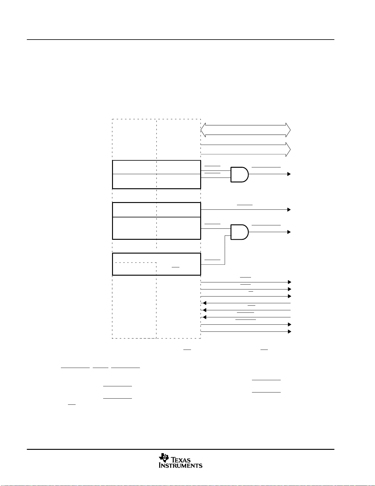
Functional Overview
ADVANCE INFORMATION
3.5 External Interface, XINTF (2812 Only)
This section gives a top-level view of the external interface (XINTF) that is implemented on the 2812 devices.
The external interface is a non-multiplexed asynchronous bus, similar to the C240x external interface. The
external interface on the 2812 is mapped into five fixed zones shown in Figure 3−4.
Figure 3−4 shows the 2812 XINTF signals.
Data Space Prog Space
0x00 0000
XD(15:0)
XA(18:0)
0x00 2000
0x00 4000
0x00 6000
0x08 0000
0x10 0000
0x18 0000
0x3F C000
0x40 0000
XINTF Zone 0
(8K × 16)
XINTF Zone 1
(8K × 16)
XINTF Zone 2
(512K × 16)
XINTF Zone 6
(512K × 16)
XINTF Zone 7
(mapped here if MP/MC
(16K × 16)
= 1)
XZCS0
XZCS1
XZCS6
XZCS7
XREADY
XMP/MC
XHOLDA
XCLKOUT (see Note E)
XZCS0AND1
XZCS2
XZCS6AND7
XWE
XRD
XR/W
XHOLD
NOTES: A. The mapping of XINTF Zone 7 is dependent on the XMP/MC device input signal and the MP/MC mode bit (bit 8 of XINTCNF2
38
register). Zones 0, 1, 2, and 6 are always enabled.
B. Each zone can be programmed with different wait states, setup and hold timing, and is supported by zone chip selects
(XZCS0AND1
glueless connection to many external memories and peripherals.
C. The chip selects for Zone 0 and 1 are ANDed internally together to form one chip select (XZCS0AND1
that is connected to XZCS0AND1
D. The chip selects for Zone 6 and 7 are ANDed internally together to form one chip select (XZCS6AND7
that is connected to XZCS6AND7
MP/MC
E. XCLKOUT is also pinned out on the 2810 and 2811.
, XZCS2, XZCS6AND7), which toggle when an access to a particular zone is performed. These features enable
). Any external memory
is dually mapped to both Zones 0 and Zone 1.
). Any external memory
is dually mapped to both Zones 6 and Zone 7. This means that if Zone 7 is disabled (via the
mode) then any external memory is still accessible via Zone 6 address space.
Figure 3−4. External Interface Block Diagram
June 2004SPRS257

Functional Overview
ADVANCE INFORMATION
The operation and timing of the external interface, can be controlled by the registers listed in Table 3−6.
Table 3−6. XINTF Configuration and Control Register Mappings
NAME ADDRESS SIZE (x16) DESCRIPTION
XTIMING0 0x00 0B20 2 XINTF Timing Register, Zone 0 can access as two 16-bit registers or one 32-bit register
XTIMING1 0x00 0B22 2 XINTF Timing Register, Zone 1 can access as two 16-bit registers or one 32-bit register
XTIMING2 0x00 0B24 2 XINTF Timing Register, Zone 2 can access as two 16-bit registers or one 32-bit register
XTIMING6 0x00 0B2C 2 XINTF Timing Register, Zone 6 can access as two 16-bit registers or one 32-bit register
XTIMING7 0x00 0B2E 2 XINTF Timing Register, Zone 7 can access as two 16-bit registers or one 32-bit register
XINTCNF2 0x00 0B34 2 XINTF Configuration Register can access as two 16-bit registers or one 32-bit register
XBANK 0x00 0B38 1 XINTF Bank Control Register
XREVISION 0x00 0B3A 1 XINTF Revision Register
3.5.1 Timing Registers
XINTF signal timing can be tuned to match specific external device requirements such as setup and hold times
to strobe signals for contention avoidance and maximizing bus efficiency. The timing parameters can be
configured individually for each zone. This allows the programmer to maximize the efficiency of the bus, based
on the type of memory or peripheral that the user needs to access. All XINTF timing values are with respect
to XTIMCLK, which is equal to or one-half of the SYSCLKOUT rate, as shown in Figure 6−25.
For detailed information on the XINTF timing and configuration register bit fields, see the TMS320F28x DSP
External Interface (XINTF) Reference Guide (literature number SPRU067).
3.5.2 XREVISION Register
The XREVISION register contains a unique number to identify the particular version of XINTF used in the
product. For the 2812, this register will be configured as described in Table 3−7.
Table 3−7. XREVISION Register Bit Definitions
BIT(S) NAME TYPE RESET DESCRIPTION
15−0 REVISION R 0x0004
Current XINTF Revision. For internal use/reference. Test purposes only. Subject to
change.
June 2004 SPRS257
39
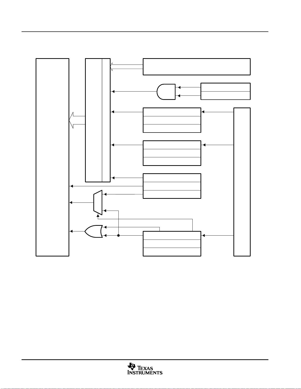
Functional Overview
ADVANCE INFORMATION
3.6 Interrupts
Figure 3−5 shows how the various interrupt sources are multiplexed within R281x devices.
INT1 to INT12
C28x CPU
INT14
INT13
PIE
†
96 Interrupts
MUX
TINT0
TINT2
TINT1
WAKEINT
Peripherals (SPI, SCI, McBSP, CAN, EV, ADC)
Interrupt Control
XINT1CR(15:0)
XINT1CTR(15:0)
Interrupt Control
XINT2CR(15:0)
XINT2CTR(15:0)
TIMER 0
TIMER 2 (for RTOS)
TIMER 1
(41 Interrupts)
WDINT
LPMINT
Watchdog
Low-Power Modes
XINT1
XINT2
GPIO
MUX
select
enable
NMI
†
Out of a possible 96 interrupts, 45 are currently used by peripherals.
Figure 3−5. Interrupt Sources
Interrupt Control
XNMICR(15:0)
XNMICTR(15:0)
XNMI_XINT13
40
June 2004SPRS257

Functional Overview
CPU
ADVANCE INFORMATION
Figure 3−6 shows how the interrupts are multiplexed using the PIE block. Eight PIE block interrupts are
grouped into one CPU interrupt. In total, 12 CPU interrupt groups, with 8 interrupts per group equals 96
possible interrupts. On R281x, 45 of these are used by peripherals as shown in Table 3−8.
INTx
PIEACKx
(Enable/Flag)
Figure 3−6. Multiplexing of Interrupts Using the PIE Block
INT1
INT2
INT11
INT12
MUX
IER(12:1)IFR(12:1)
(Enable)(Flag)
(Enable) (Flag)
PIEIERx(8:1) PIEIFRx(8:1)
MUX
INTx.1
INTx.2
INTx.3
INTx.4
INTx.5
INTx.6
INTx.7
INTx.8
INTM
1
0
Global
Enable
From
Peripherals or
External
Interrupts
CPU
(EV-A)
(EV-A)
(EV-B)
(EV-B)
†
CMP3INT
CMP6INT
SCIRXINTB
(EV-A)
T2UFINT
(EV-A)
(EV-B)
T4UFINT
(EV-B)
(SCI-B)
PDPINTB
(EV-B)
CMP2INT
(EV-A)
T2CINT
(EV-A)
CMP5INT
(EV-B)
T4CINT
(EV-B)
SPITXINTA
(SPI)
SCITXINTA
(SCI-A)
PDPINTA
(EV-A)
CMP1INT
(EV-A)
T2PINT
(EV-A)
CMP4INT
(EV-B)
T4PINT
(EV-B)
SPIRXINTA
(SPI)
SCIRXINTA
(SCI-A)
Table 3−8. PIE Peripheral Interrupts
CPU
INTERRUPTS
INT1
INT2 reserved
INT3 reserved
INT4 reserved
INT5 reserved
INT6 reserved reserved
INT7 reserved reserved reserved reserved reserved reserved reserved reserved
INT8 reserved reserved reserved reserved reserved reserved reserved reserved
INT9 reserved reserved
INT10 reserved reserved reserved reserved reserved reserved reserved reserved
INT11 reserved reserved reserved reserved reserved reserved reserved reserved
INT12 reserved reserved reserved reserved reserved reserved reserved reserved
†
Out of the 96 possible interrupts, 45 interrupts are currently used. the remaining interrupts are reserved for future devices. However, these
interrupts can be used as software interrupts if they are enabled at the PIEIFRx level.
INTx.8 INTx.7 INTx.6 INTx.5 INTx.4 INTx.3 INTx.2 INTx.1
WAKEINT
(LPM/WD)
TINT0
(TIMER 0)
T1OFINT
(EV-A)
CAPINT3
(EV-A)
T3OFINT
(EV-B)
CAPINT6
(EV-B)
ADCINT
(ADC)
T1UFINT
(EV-A)
CAPINT2
(EV-A)
T3UFINT
(EV-B)
CAPINT5
(EV-B)
MXINT
(McBSP)
ECAN1INT
(CAN)
PIE INTERRUPTS
XINT2 XINT1 reserved
T1CINT
(EV-A)
CAPINT1
(EV-A)
T3CINT
(EV-B)
CAPINT4
(EV-B)
MRINT
(McBSP)
ECAN0INT
(CAN)
T1PINT
T2OFINT
T3PINT
T4OFINT
reserved reserved
SCITXINTB
(SCI-B)
June 2004 SPRS257
41

Functional Overview
ADVANCE INFORMATION
Table 3−9. PIE Configuration and Control Registers
NAME ADDRESS
PIECTRL 0x0000−0CE0 1 PIE, Control Register
PIEACK 0x0000−0CE1 1 PIE, Acknowledge Register
PIEIER1 0x0000−0CE2 1 PIE, INT1 Group Enable Register
PIEIFR1 0x0000−0CE3 1 PIE, INT1 Group Flag Register
PIEIER2 0x0000−0CE4 1 PIE, INT2 Group Enable Register
PIEIFR2 0x0000−0CE5 1 PIE, INT2 Group Flag Register
PIEIER3 0x0000−0CE6 1 PIE, INT3 Group Enable Register
PIEIFR3 0x0000−0CE7 1 PIE, INT3 Group Flag Register
PIEIER4 0x0000−0CE8 1 PIE, INT4 Group Enable Register
PIEIFR4 0x0000−0CE9 1 PIE, INT4 Group Flag Register
PIEIER5 0x0000−0CEA 1 PIE, INT5 Group Enable Register
PIEIFR5 0x0000−0CEB 1 PIE, INT5 Group Flag Register
PIEIER6 0x0000−0CEC 1 PIE, INT6 Group Enable Register
PIEIFR6 0x0000−0CED 1 PIE, INT6 Group Flag Register
PIEIER7 0x0000−0CEE 1 PIE, INT7 Group Enable Register
PIEIFR7 0x0000−0CEF 1 PIE, INT7 Group Flag Register
Size (x16)
DESCRIPTION
PIEIER8 0x0000−0CF0 1 PIE, INT8 Group Enable Register
PIEIFR8 0x0000−0CF1 1 PIE, INT8 Group Flag Register
PIEIER9 0x0000−0CF2 1 PIE, INT9 Group Enable Register
PIEIFR9 0x0000−0CF3 1 PIE, INT9 Group Flag Register
PIEIER10 0x0000−0CF4 1 PIE, INT10 Group Enable Register
PIEIFR10 0x0000−0CF5 1 PIE, INT10 Group Flag Register
PIEIER11 0x0000−0CF6 1 PIE, INT11 Group Enable Register
PIEIFR11 0x0000−0CF7 1 PIE, INT11 Group Flag Register
PIEIER12 0x0000−0CF8 1 PIE, INT12 Group Enable Register
PIEIFR12 0x0000−0CF9 1 PIE, INT12 Group Flag Register
Reserved 0x0000−0CFA
0x0000−0CFF
Note: The PIE configuration and control registers are not protected by EALLOW mode. The PIE vector table is protected.
6 Reserved
42
June 2004SPRS257

3.6.1 External Interrupts
ADVANCE INFORMATION
Table 3−10. External Interrupt Registers
NAME ADDRESS SIZE (x16) DESCRIPTION
XINT1CR 0x00 7070 1 XINT1 control register
XINT2CR 0x00 7071 1 XINT2 control register
reserved
XNMICR 0x00 7077 1 XNMI control register
XINT1CTR 0x00 7078 1 XINT1 counter register
XINT2CTR 0x00 7079 1 XINT2 counter register
reserved
XNMICTR 0x00 707F 1 XNMI counter register
Each external interrupt can be enabled/disabled or qualified using positive or negative going edge. For more
information, see the TMS320F28x System Control and Interrupts Reference Guide (literature number
SPRU078).
0x00 7072
0x00 7076
0x00 707A
0x00 707E
5
5
Functional Overview
June 2004 SPRS257
43

Functional Overview
ADVANCE INFORMATION
3.7 System Control
This section describes R281x oscillator, PLL and clocking mechanisms, the watchdog function and the low
power modes. Figure 3−7 shows the various clock and reset domains in R281x devices that will be discussed.
Reset
SYSCLKOUT
Peripheral Reset
Watchdog
Block
XRS
C28x
CPU
Peripheral Bus
System
Control
Registers
Peripheral
Registers
Low-Speed Prescaler
Peripheral
Registers
High-Speed Prescaler
Peripheral
Registers
CLKIN
Clock Enables
eCAN
LSPCLK
Low-Speed Peripherals
SCI-A/B, SPI, McBSP
HSPCLK
High-Speed Peripherals
EV-A/B
PLL
Power
Modes
Control
I/O
I/O
I/O
OSC
GPIO
MUX
X1/XCLKIN
X2
XF_XPLLDIS
GPIOs
44
HSPCLK
ADC
Registers
NOTE A: CLKIN is the clock input to the CPU. SYSCLKOUT is the output clock of the CPU. They are of the same frequency.
12-Bit ADC
16 ADC Inputs
Figure 3−7. Clock and Reset Domains
The PLL, clocking, watchdog and low-power modes are controlled by the registers listed in Table 3−11.
June 2004SPRS257

Functional Overview
ADVANCE INFORMATION
Table 3−11. PLL, Clocking, Watchdog, and Low-Power Mode Registers
NAME
reserved
reserved 0x00 7018 1
reserved 0x00 7019 1
HISPCP 0x00 701A 1 High-Speed Peripheral Clock Prescaler Register for HSPCLK clock
LOSPCP 0x00 701B 1 Low-Speed Peripheral Clock Prescaler Register for LSPCLK clock
PCLKCR 0x00 701C 1 Peripheral Clock Control Register
reserved 0x00 701D 1
LPMCR0 0x00 701E 1 Low Power Mode Control Register 0
LPMCR1 0x00 701F 1 Low Power Mode Control Register 1
reserved 0x00 7020 1
PLLCR 0x00 7021 1 PLL Control Register
SCSR 0x00 7022 1 System Control & Status Register
WDCNTR 0x00 7023 1 Watchdog Counter Register
reserved 0x00 7024 1
WDKEY 0x00 7025 1 Watchdog Reset Key Register
reserved
WDCR 0x00 7029 1 Watchdog Control Register
reserved
†
All of the above registers can only be accessed, by executing the EALLOW instruction.
‡
The PLL control register (PLLCR) is reset to a known state by the XRS signal only. Emulation reset (through Code Composer Studio) will not
reset PLLCR.
ADDRESS SIZE (x16) DESCRIPTION
0x00 7010
0x00 7017
0x00 7026
0x00 7028
0x00 702A
0x00 702F
8
‡
3
6
†
3.7.1 OSC and PLL Block
Figure 3−8 shows the OSC and PLL block on R281x.
June 2004 SPRS257
45

Functional Overview
T
ADVANCE INFORMATION
XF_XPLLDIS
XCLKIN
X1/XCLKIN
On-Chip
Oscillator
(OSC)
X2
Latch
XRS
OSCCLK (PLL Disabled)
PLL
Bypass
4-Bit PLL Select
PLL
4-Bit PLL Select
XPLLDIS
/2
0
1
PLL Block
CLKIN
CPU
Figure 3−8. OSC and PLL Block
The on-chip oscillator circuit enables a crystal to be attached to R281x devices using the X1/XCLKIN and X2
pins. If a crystal is not used, then an external oscillator can be directly connected to the X1/XCLKIN pin and
the X2 pin is left unconnected. The logic-high level in this case should not exceed V
. The PLLCR bits [3:0]
DD
set the clocking ratio.
Table 3−12. PLLCR Register Bit Definitions
BIT(S) NAME TYPE XRS RESET
15:4 reserved R = 0 0:0
†
SYSCLKOUT = (XCLKIN * n)/2, where n is the PLL multiplication factor.
DESCRIPTION
SYSCLKOU
†
3.7.2 Loss of Input Clock
Bit Value n SYSCLKOUT
0000 PLL Bypassed XCLKIN/2
0001 1 XCLKIN/2
0010 2 XCLKIN
0011 3 XCLKIN * 1.5
0100 4 XCLKIN * 2
3:0 DIV R/W 0,0,0,0
The PLLCR register is reset to a known state by the XRS reset line. If a reset is issued by the debugger, the PLL clocking ratio is not changed.
In PLL enabled mode, if the input clock XCLKIN or the oscillator clock is removed or absent, the PLL will still
0101 5 XCLKIN * 2.5
0110 6 XCLKIN * 3
0111 7 XCLKIN * 3.5
1000 8 XCLKIN * 4
1001 9 XCLKIN * 4.5
1010 10 XCLKIN * 5
1011 11 Reserved
1100 12 Reserved
1101 13 Reserved
1110 14 Reserved
1111 15 Reserved
issue a “limp-mode” clock. The limp-mode clock will continue to clock the CPU and peripherals at a typical
frequency of 1−4 MHz. The PLLCR register should have been written to with a non-zero value for this feature
to work.
46
June 2004SPRS257

Normally, when the input clocks are present, the watchdog counter will decrement to initiate a watchdog reset
ADVANCE INFORMATION
or WDINT interrupt. However, when the external input clock fails, the watchdog counter will stop decrementing
(i.e., the watchdog counter does not change with the limp-mode clock). This condition could be used by the
application firmware to detect the input clock failure and initiate necessary shut-down procedure for the
system.
3.7.3 PLL-Based Clock Module
R281x has an on-chip, PLL-based clock module. This module provides all the necessary clocking signals for
the device, as well as control for low-power mode entry. The PLL has a 4-bit ratio control to select different
CPU clock rates. The watchdog module should be disabled before writing to the PLLCR register. It can be
re-enabled (if need be) after the PLL module has stabilized, which takes 131072 XCLKIN cycles.
The PLL-based clock module provides two modes of operation:
• Crystal-operation
This mode allows the use of an external crystal/resonator to provide the time base to the device.
• External clock source operation
This mode allows the internal oscillator to be bypassed. The device clocks are generated from an external
clock source input on the X1/XCLKIN pin.
Functional Overview
X2X1/XCLKIN X1/XCLKIN X2
C
(see Note A)
NOTE A: TI recommends that customers have the resonator/crystal vendor characterize the operation of their device with the DSP chip. The
resonator/crystal vendor has the equipment and expertise to tune the tank circuit. The vendor can also advise the customer regarding
the proper tank component values that will ensure start-up and stability over the entire operating range.
b1
Crystal
(a) (b)
C
b2
(see Note A)
External Clock Signal
(Toggling 0−V
DD
)
NC
Figure 3−9. Recommended Crystal/Clock Connection
Table 3−13. Possible PLL Configuration Modes
PLL MODE REMARKS SYSCLKOUT
Invoked by tying XPLLDIS pin low upon reset. PLL block is completely
PLL Disabled
PLL Bypassed
PLL Enabled
disabled. Clock input to the CPU (CLKIN) is directly derived from the clock
signal present at the X1/XCLKIN pin.
Default PLL configuration upon power-up, if PLL is not disabled. The PLL
itself is bypassed. However, the /2 module in the PLL block divides the clock
input at the X1/XCLKIN pin by two before feeding it to the CPU.
Achieved by writing a non-zero value “n” into PLLCR register. The /2 module
in the PLL block now divides the output of the PLL by two before feeding it to
the CPU.
XCLKIN
XCLKIN/2
(XCLKIN * n) / 2
3.7.4 External Reference Oscillator Clock Option
The typical specifications for the external quartz crystal for a frequency of 30 MHz are listed below:
• Fundamental mode, parallel resonant
(load capacitance) = 12 pF
• C
L
= C
• C
• C
L1
shunt
= 24 pF
L2
= 6 pF
• ESR range = 25 to 40 Ω
June 2004 SPRS257
47
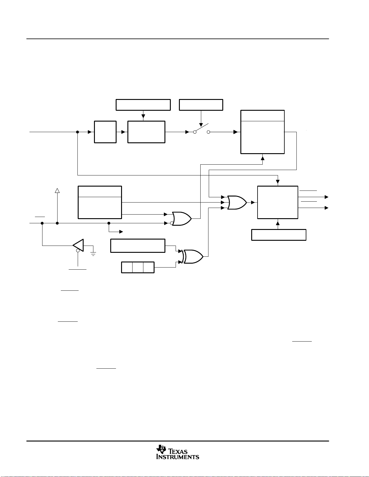
Functional Overview
ADVANCE INFORMATION
3.7.5 Watchdog Block
The watchdog block on R281x is identical to the one used on the 240x devices. The watchdog module
generates an output pulse, 512 oscillator clocks wide (OSCCLK), whenever the 8-bit watchdog up counter
has reached its maximum value. To prevent this, the user disables the counter or the software must
periodically write a 0x55 + 0xAA sequence into the watchdog key register which will reset the watchdog
counter. Figure 3−10 shows the various functional blocks within the watchdog module.
OSCCLK
Internal
XRS
Pullup
WDKEY(7:0)
Key Detector
WDRST
(See Note A)
/512
Watchdog
55 + AA
WDCR (WDPS(2:0))
Watchdog
Prescaler
Bad Key
Good Key
Core-reset
WDCR (WDCHK(2:0))
1 0 1
WDCLK
WDCR (WDDIS)
Clear Counter
Bad
WDCHK
Key
WDCNTR(7:0)
8-Bit
Watchdog
Counter
CLR
Generate
Output Pulse
(512 OSCCLKs)
SCSR (WDENINT)
WDRST
WDINT
NOTE A: The WDRST signal is driven low for 512 OSCCLK cycles.
3.7.6 Low-Power Modes Block
48
Figure 3−10. Watchdog Module
The WDINT
signal enables the watchdog to be used as a wakeup from IDLE/STANDBY mode timer.
In STANDBY mode, all peripherals are turned off on the device. The only peripheral that remains functional
is the watchdog. The Watchdog module will run off the PLL clock or the oscillator clock. The WDINT
signal
is fed to the LPM block so that it can wake the device from STANDBY (if enabled). See Section 3.7.6,
Low-Power Modes Block, for more details.
In IDLE mode, the WDINT
signal can generate an interrupt to the CPU, via the PIE, to take the CPU out of
IDLE mode.
In HALT mode, this feature cannot be used because the oscillator (and PLL) are turned off and hence so is
the WATCHDOG.
The low-power modes on R281x are similar to the 240x devices. Table 3−14 summarizes the various modes.
June 2004SPRS257
Functional Overview
ADVANCE INFORMATION
Table 3−14. R281x Low-Power Modes
MODE LPM(1:0) OSCCLK CLKIN SYSCLKOUT EXIT
Normal X,X on on on −
IDLE 0,0 on on on
on
STANDBY 0,1
HALT 1,X
†
The Exit column lists which signals or under what conditions the low power mode will be exited. A low signal, on any of the signals, will exit the
low power condition. This signal must be kept low long enough for an interrupt to be recognized by the device. Otherwise the IDLE mode will not
be exited and the device will go back into the indicated low power mode.
‡
The IDLE mode on the C28x behaves differently than on the 24x/240x. On the C28x, the clock output from the core (SYSCLKOUT) is still functional
while on the 24x/240x the clock is turned off.
§
On the C28x, the JTAG port can still function even if the core clock (CLKIN) is turned off.
(watchdog still running)
off
(oscillator and PLL turned off,
watchdog not functional)
off off
off off
‡
Any Enabled Interrupt,
T1/2/3/4CTRIP
C1/2/3/4/5/6TRIP
†
XRS,
WDINT
XNMI
Debugger
XRS,
WDINT
XINT1,
XNMI,
SCIRXDA,
SCIRXDB,
CANRX,
Debugger
XRS,
XNMI,
Debugger
,
§
,
,
,
§
§
The various low-power modes operate as follows:
IDLE Mode: This mode is exited by any enabled interrupt or an XNMI that is
recognized by the processor. The LPM block performs no tasks during
this mode as long as the LPMCR0(LPM) bits are set to 0,0.
STANDBY Mode: All other signals (including XNMI) will wake the device from STANDBY
mode if selected by the LPMCR1 register. The user will need to select
which signal(s) will wake the device. The selected signal(s) are also
qualified by the OSCCLK before waking the device. The number of
OSCCLKs is specified in the LPMCR0 register.
HALT Mode: Only the XRS
and XNMI external signals can wake the device from
HALT mode. The XNMI input to the core has an enable/disable bit.
Hence, it is safe to use the XNMI signal for this function.
NOTE: The low-power modes do not affect the state of the output pins (PWM pins included). They will be
in whatever state the code left them when the IDLE instruction was executed.
June 2004 SPRS257
49

Peripherals
ADVANCE INFORMATION
4 Peripherals
The integrated peripherals of R281x are described in the following subsections:
• Three 32-bit CPU-Timers
• Two event-manager modules (EVA, EVB)
• Enhanced analog-to-digital converter (ADC) module
• Enhanced controller area network (eCAN) module
• Multichannel buffered serial port (McBSP) module
• Serial communications interface modules (SCI-A, SCI-B)
• Serial peripheral interface (SPI) module
• Digital I/O and shared pin functions
4.1 32-Bit CPU-Timers 0/1/2
There are three 32-bit CPU-timers on R281x devices (CPU-TIMER0/1/2).
CPU-Timer 2 is reserved for the real-time OS (such as DSP/BIOS). CPU-Timer 0/1 can be used in user
applications. These timers are different from the general-purpose (GP) timers that are present in the Event
Manager modules (EVA, EVB).
NOTE: If the application is not using DSP/BIOS, then CPU-Timers 1 and 2 can be used in the
application.
Reset
Timer Reload
SYSCLKOUT
TCR.4
(Timer Start Status)
TINT
16-Bit Timer Divide-Down
TDDRH:TDDR
16-Bit Prescale Counter
PSCH:PSC
Borrow
32-Bit Timer Period
Figure 4−1. CPU-Timers
PRDH:PRD
32-Bit Counter
TIMH:TIM
Borrow
50
June 2004SPRS257
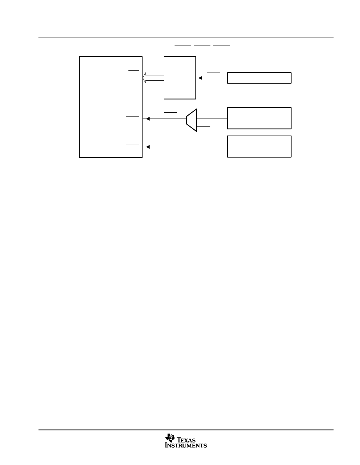
Peripherals
ADVANCE INFORMATION
In R281x devices, the timer interrupt signals (TINT0, TINT1, TINT2) are connected as shown in Figure 4−2.
INT1
to
INT12
C28x
INT13
INT14
NOTES: A. The timer registers are connected to the Memory Bus of the C28x processor.
B. The timing of the timers is synchronized to SYSCLKOUT of the processor clock.
PIE
TINT1
TINT2
TINT0
XINT13
CPU-TIMER 0
CPU-TIMER 1
CPU-TIMER 2
Reserved RTOS
(DSP/BIOS)
Figure 4−2. CPU-Timer Interrupts Signals and Output Signal (See Notes A and B)
The general operation of the timer is as follows: The 32-bit counter register “TIMH:TIM” is loaded with the value
in the period register “PRDH:PRD”. The counter register, decrements at the SYSCLKOUT rate of the C28x.
When the counter reaches 0, a timer interrupt output signal generates an interrupt pulse. The registers listed
in Table 4−1 are used to configure the timers. For more information, see the TMS320F28x System Control
and Interrupts Reference Guide (literature number SPRU078).
June 2004 SPRS257
51

Peripherals
ADVANCE INFORMATION
Table 4−1. CPU-Timers 0, 1, 2 Configuration and Control Registers
NAME ADDRESS SIZE (x16) DESCRIPTION
TIMER0TIM 0x00 0C00 1 CPU-Timer 0, Counter Register
TIMER0TIMH 0x00 0C01 1 CPU-Timer 0, Counter Register High
TIMER0PRD 0x00 0C02 1 CPU-Timer 0, Period Register
TIMER0PRDH 0x00 0C03 1 CPU-Timer 0, Period Register High
TIMER0TCR 0x00 0C04 1 CPU-Timer 0, Control Register
reserved 0x00 0C05 1
TIMER0TPR 0x00 0C06 1 CPU-Timer 0, Prescale Register
TIMER0TPRH 0x00 0C07 1 CPU-Timer 0, Prescale Register High
TIMER1TIM 0x00 0C08 1 CPU-Timer 1, Counter Register
TIMER1TIMH 0x00 0C09 1 CPU-Timer 1, Counter Register High
TIMER1PRD 0x00 0C0A 1 CPU-Timer 1, Period Register
TIMER1PRDH 0x00 0C0B 1 CPU-Timer 1, Period Register High
TIMER1TCR 0x00 0C0C 1 CPU-Timer 1, Control Register
reserved 0x00 0C0D 1
TIMER1TPR 0x00 0C0E 1 CPU-Timer 1, Prescale Register
TIMER1TPRH 0x00 0C0F 1 CPU-Timer 1, Prescale Register High
TIMER2TIM 0x00 0C10 1 CPU-Timer 2, Counter Register
TIMER2TIMH 0x00 0C11 1 CPU-Timer 2, Counter Register High
TIMER2PRD 0x00 0C12 1 CPU-Timer 2, Period Register
TIMER2PRDH 0x00 0C13 1 CPU-Timer 2, Period Register High
TIMER2TCR 0x00 0C14 1 CPU-Timer 2, Control Register
reserved 0x00 0C15 1
TIMER2TPR 0x00 0C16 1 CPU-Timer 2, Prescale Register
TIMER2TPRH 0x00 0C17 1 CPU-Timer 2, Prescale Register High
reserved
0x00 0C18
0x00 0C3F
40
4.2 Event Manager Modules (EVA, EVB)
52
The event-manager modules include general-purpose (GP) timers, full-compare/PWM units, capture units,
and quadrature-encoder pulse (QEP) circuits. EVA and EVB timers, compare units, and capture units function
identically. However, timer/unit names differ for EVA and EVB. Table 4−2 shows the module and signal names
used. Table 4−2 shows the features and functionality available for the event-manager modules and highlights
EVA nomenclature.
Event managers A and B have identical peripheral register sets with EVA starting at 7400h and EVB starting
at 7500h. The paragraphs in this section describe the function of GP timers, compare units, capture units, and
QEPs using EVA nomenclature. These paragraphs are applicable to EVB with regard to function—however,
module/signal names would differ. Table 4−3 lists the EVA registers. For more information, see the
TMS320F28x DSP Event Manager (EV) Reference Guide (literature number SPRU065).
June 2004SPRS257
Table 4−2. Module and Signal Names for EVA and EVB
ADVANCE INFORMATION
Peripherals
EVENT MANAGER MODULES
GP Timers
Compare Units
Capture Units
QEP Channels
External Clock Inputs
External Trip Inputs Compare
External Trip Inputs
†
In the 24x/240x-compatible mode, the T1CTRIP_PDPINTA pin functions as PDPINTA and the T3CTRIP_PDPINTB pin functions as PDPINTB.
MODULE SIGNAL MODULE SIGNAL
GP Timer 1
GP Timer 2
Compare 1
Compare 2
Compare 3
Capture 1
Capture 2
Capture 3
QEP1
QEP2
QEPI1
Direction
External Clock
EVA EVB
T1PWM/T1CMP
T2PWM/T2CMP
PWM1/2
PWM3/4
PWM5/6
CAP1
CAP2
CAP3
QEP1
QEP2
TDIRA
TCLKINA
C1TRIP
C2TRIP
C3TRIP
T1CTRIP_PDPINTA
T2CTRIP/EVASOC
†
GP Timer 3
GP Timer 4
Compare 4
Compare 5
Compare 6
Capture 4
Capture 5
Capture 6
QEP3
QEP4
QEPI2
Direction
External Clock
Compare
T3PWM/T3CMP
T4PWM/T4CMP
PWM7/8
PWM9/10
PWM11/12
CAP4
CAP5
CAP6
QEP3
QEP4
TDIRB
TCLKINB
C4TRIP
C5TRIP
C6TRIP
T3CTRIP_PDPINTB
T4CTRIP/EVBSOC
†
June 2004 SPRS257
53
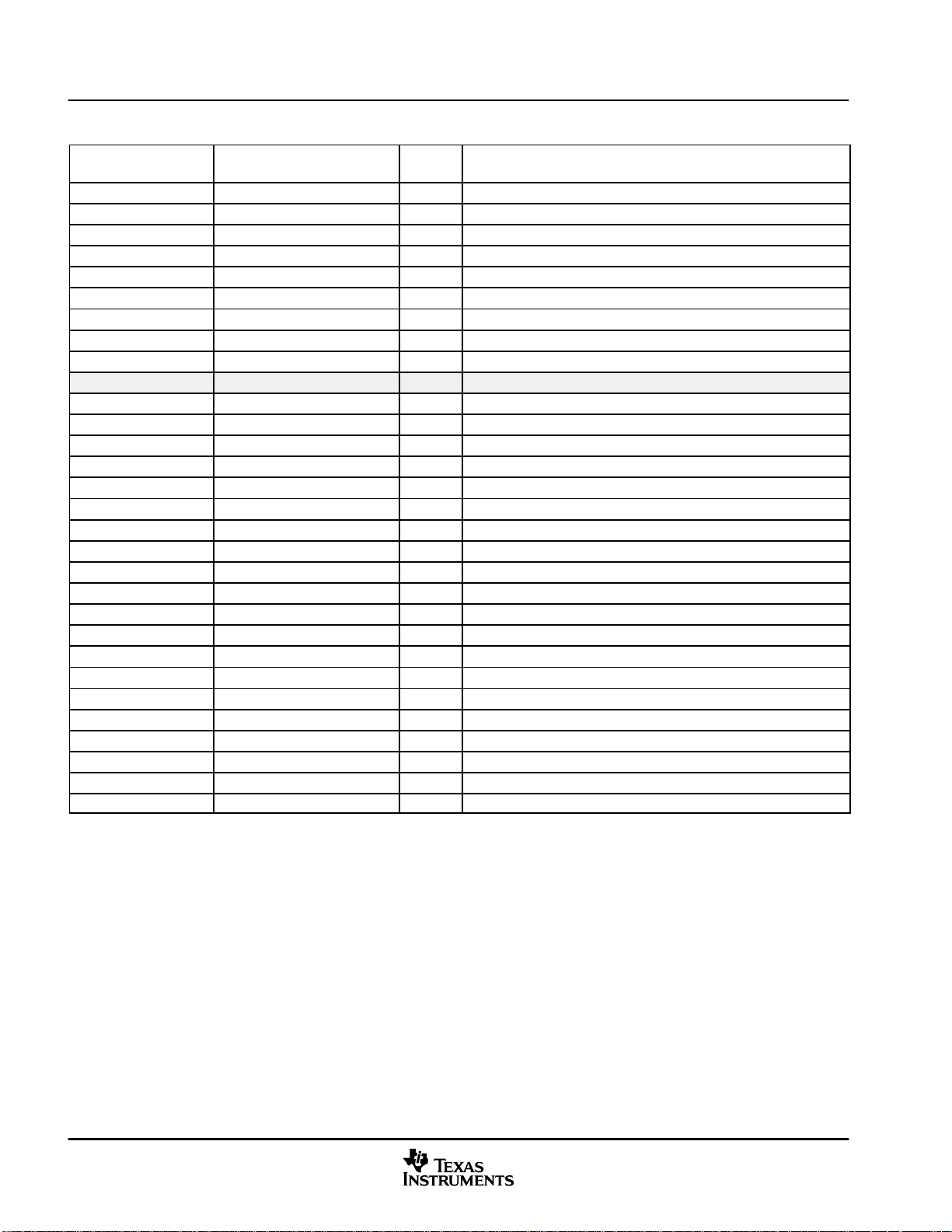
Peripherals
ADVANCE INFORMATION
Table 4−3. EVA Registers
NAME
GPTCONA 0x00 7400 1 GP Timer Control Register A
T1CNT 0x00 7401 1 GP Timer 1 Counter Register
T1CMPR 0x00 7402 1 GP Timer 1 Compare Register
T1PR 0x00 7403 1 GP Timer 1 Period Register
T1CON 0x00 7404 1 GP Timer 1 Control Register
T2CNT 0x00 7405 1 GP Timer 2 Counter Register
T2CMPR 0x00 7406 1 GP Timer 2 Compare Register
T2PR 0x00 7407 1 GP Timer 2 Period Register
T2CON 0x00 7408 1 GP Timer 2 Control Register
EXTCONA
COMCONA 0x00 7411 1 Compare Control Register A
ACTRA 0x00 7413 1 Compare Action Control Register A
DBTCONA 0x00 7415 1 Dead-Band Timer Control Register A
CMPR1 0x00 7417 1 Compare Register 1
CMPR2 0x00 7418 1 Compare Register 2
CMPR3 0x00 7419 1 Compare Register 3
CAPCONA 0x00 7420 1 Capture Control Register A
CAPFIFOA 0x00 7422 1 Capture FIFO Status Register A
CAP1FIFO 0x00 7423 1 Two-Level Deep Capture FIFO Stack 1
CAP2FIFO 0x00 7424 1 Two-Level Deep Capture FIFO Stack 2
CAP3FIFO 0x00 7425 1 Two-Level Deep Capture FIFO Stack 3
CAP1FBOT 0x00 7427 1 Bottom Register Of Capture FIFO Stack 1
CAP2FBOT 0x00 7428 1 Bottom Register Of Capture FIFO Stack 2
CAP3FBOT 0x00 7429 1 Bottom Register Of Capture FIFO Stack 3
EVAIMRA 0x00 742C 1 Interrupt Mask Register A
EVAIMRB 0x00 742D 1 Interrupt Mask Register B
EVAIMRC 0x00 742E 1 Interrupt Mask Register C
EVAIFRA 0x00 742F 1 Interrupt Flag Register A
EVAIFRB 0x00 7430 1 Interrupt Flag Register B
EVAIFRC 0x00 7431 1 Interrupt Flag Register C
†
The EV-B register set is identical except the address range is from 0x00−7500 to 0x00−753F. The above registers are mapped to Zone 2. This
space allows only 16-bit accesses. 32-bit accesses produce undefined results.
‡
New register compared to 24x/240x
‡
ADDRESS
0x00 7409 1 GP Extension Control Register A
SIZE
(x16)
†
DESCRIPTION
54
June 2004SPRS257

Peripheral Write Bus
ADVANCE INFORMATION
Peripherals
MXINT
To CPU
LSPCLK
MRINT
To CPU
TX Interrupt Logic
McBSP Transmit
Interrupt Select Logic
McBSP Registers
and Control Logic
McBSP
McBSP Receive
Interrupt Select Logic
RX Interrupt Logic
TX FIFO
Interrupt
RX FIFO
Interrupt
TX FIFO _15
—
TX FIFO _1
TX FIFO _0
TX FIFO Registers
16
DXR2 Transmit Buffer
16
XSR2
RSR2
16
16
DRR2 Receive Buffer
16
RX FIFO _15
—
RX FIFO _1
RX FIFO _0
RX FIFO Registers
TX FIFO _15
—
TX FIFO _1
TX FIFO _0
16
DXR1 Transmit Buffer
16
Compand Logic
XSR1
RSR1
16
Expand Logic
RBR1 RegisterRBR2 Register
16
DRR1 Receive Buffer
16
RX FIFO _15
—
RX FIFO _1
RX FIFO _0
FSX
CLKX
DX
DR
CLKR
FSR
Peripheral Read Bus
Figure 4−3. Event Manager A Functional Block Diagram (See Note A)
4.2.1 General-Purpose (GP) Timers
There are two GP timers. The GP timer x (x = 1 or 2 for EVA; x = 3 or 4 for EVB) includes:
• A 16-bit timer, up-/down-counter, TxCNT, for reads or writes
• A 16-bit timer-compare register, TxCMPR (double-buffered with shadow register), for reads or writes
• A 16-bit timer-period register, TxPR (double-buffered with shadow register), for reads or writes
• A 16-bit timer-control register,TxCON, for reads or writes
• Selectable internal or external input clocks
June 2004 SPRS257
55

Peripherals
ADVANCE INFORMATION
• A programmable prescaler for internal or external clock inputs
• Control and interrupt logic, for four maskable interrupts: underflow, overflow, timer compare, and period
interrupts
• A selectable direction input pin (TDIRx) (to count up or down when directional up-/ down-count mode is
selected)
The GP timers can be operated independently or synchronized with each other. The compare register
associated with each GP timer can be used for compare function and PWM-waveform generation. There are
three continuous modes of operations for each GP timer in up- or up/ down-counting operations. Internal or
external input clocks with programmable prescaler are used for each GP timer. GP timers also provide the
time base for the other event-manager submodules: GP timer 1 for all the compares and PWM circuits, GP
timer 2/1 for the capture units and the quadrature-pulse counting operations. Double-buffering of the period
and compare registers allows programmable change of the timer (PWM) period and the compare/PWM pulse
width as needed.
4.2.2 Full-Compare Units
There are three full-compare units on each event manager. These compare units use GP timer1 as the time
base and generate six outputs for compare and PWM-waveform generation using programmable deadband
circuit. The state of each of the six outputs is configured independently. The compare registers of the compare
units are double-buffered, allowing programmable change of the compare/PWM pulse widths as needed.
4.2.3 Programmable Deadband Generator
4.2.4 PWM Waveform Generation
4.2.5 Double Update PWM Mode
4.2.6 PWM Characteristics
Deadband generation can be enabled/disabled for each compare unit output individually. The
deadband-generator circuit produces two outputs (with or without deadband zone) for each compare unit
output signal. The output states of the deadband generator are configurable and changeable as needed by
way of the double-buffered ACTRx register.
Up to eight PWM waveforms (outputs) can be generated simultaneously by each event manager: three
independent pairs (six outputs) by the three full-compare units with programmable deadbands, and two
independent PWMs by the GP-timer compares.
The R281x Event Manager supports “Double Update PWM Mode.” This mode refers to a PWM operation
mode in which the position of the leading edge and the position of the trailing edge of a PWM pulse are
independently modifiable in each PWM period. To support this mode, the compare register that determines
the position of the edges of a PWM pulse must allow (buffered) compare value update once at the beginning
of a PWM period and another time in the middle of a PWM period. The compare registers in R281x Event
Managers are all buffered and support three compare value reload/update (value in buffer becoming active)
modes. These modes have earlier been documented as compare value reload conditions. The reload
condition that supports double update PWM mode is reloaded on Underflow (beginning of PWM period) OR
Period (middle of PWM period). Double update PWM mode can be achieved by using this condition for
compare value reload.
Characteristics of the PWMs are as follows:
56
• 16-bit registers
• Wide range of programmable deadband for the PWM output pairs
• Change of the PWM carrier frequency for PWM frequency wobbling as needed
June 2004SPRS257

Peripherals
ADVANCE INFORMATION
• Change of the PWM pulse widths within and after each PWM period as needed
• External-maskable power and drive-protection interrupts
• Pulse-pattern-generator circuit, for programmable generation of asymmetric, symmetric, and four-space
vector PWM waveforms
• Minimized CPU overhead using auto-reload of the compare and period registers
• The PWM pins are driven to a high-impedance state when the PDPINTx
PDPINTx
register.
− PDPINTA
− PDPINTB
• EXTCON register bits provide options to individually trip control for each PWM pair of signals
signal qualification. The PDPINTx pin (after qualification) is reflected in bit 8 of the COMCONx
4.2.7 Capture Unit
The capture unit provides a logging function for different events or transitions. The values of the selected GP
timer counter is captured and stored in the two-level-deep FIFO stacks when selected transitions are detected
on capture input pins, CAPx (x = 1, 2, or 3 for EVA; and x = 4, 5, or 6 for EVB). The capture unit consists of
three capture circuits.
• Capture units include the following features:
− One 16-bit capture control register, CAPCONx (R/W)
− One 16-bit capture FIFO status register, CAPFIFOx
− Selection of GP timer 1/2 (for EVA) or 3/4 (for EVB) as the time base
− Three 16-bit 2-level-deep FIFO stacks, one for each capture unit
− Three capture input pins (CAP1/2/3 for EVA, CAP4/5/6 for EVB)—one input pin per capture unit. [All
inputs are synchronized with the device (CPU) clock. In order for a transition to be captured, the input
must hold at its current level to meet the input qualification circuitry requirements. The input pins
CAP1/2 and CAP4/5 can also be used as QEP inputs to the QEP circuit.]
pin is driven low and after
pin status is reflected in bit 8 of COMCONA register.
pin status is reflected in bit 8 of COMCONB register.
− User-specified transition (rising edge, falling edge, or both edges) detection
− Three maskable interrupt flags, one for each capture unit
− The capture pins can also be used as general-purpose interrupt pins, if they are not used for the
capture function.
4.2.8 Quadrature-Encoder Pulse (QEP) Circuit
Two capture inputs (CAP1 and CAP2 for EVA; CAP4 and CAP5 for EVB) can be used to interface the on-chip
QEP circuit with a quadrature encoder pulse. Full synchronization of these inputs is performed on-chip.
Direction or leading-quadrature pulse sequence is detected, and GP timer 2/4 is incremented or decremented
by the rising and falling edges of the two input signals (four times the frequency of either input pulse).
With EXTCONA register bits, the EVA QEP circuit can use CAP3 as a capture index pin as well. Similarly, with
EXTCONB register bits, the EVB QEP circuit can use CAP6 as a capture index pin.
4.2.9 External ADC Start-of-Conversion
EVA/EVB start-of-conversion (SOC) can be sent to an external pin (EVASOC/EVBSOC) for external ADC
interface. EVASOC
June 2004 SPRS257
and EVBSOC are MUXed with T2CTRIP and T4CTRIP, respectively.
57

Peripherals
ADVANCE INFORMATION
4.3 Enhanced Analog-to-Digital Converter (ADC) Module
A simplified functional block diagram of the ADC module is shown in Figure 4−4. The ADC module consists
of a 12-bit ADC with a built-in sample-and-hold (S/ H) circuit. Functions of the ADC module include:
• 12-bit ADC core with built-in S/H
• Analog input: 0.0 V to 3.0 V (Voltages above 3.0 V produce full-scale conversion results.)
• Fast conversion rate: 80 ns at 25-MHz ADC clock, 12.5 MSPS
• 16-channel, MUXed inputs
• Autosequencing capability provides up to 16 “autoconversions” in a single session. Each conversion can
be programmed to select any 1 of 16 input channels
• Sequencer can be operated as two independent 8-state sequencers or as one large 16-state sequencer
(i.e., two cascaded 8-state sequencers)
• Sixteen result registers (individually addressable) to store conversion values
− The digital value of the input analog voltage is derived by:
Digital Value + 4095
• Multiple triggers as sources for the start-of-conversion (SOC) sequence
Input Analog Voltage * ADCLO
3
− S/W − software immediate start
− EVA − Event manager A (multiple event sources within EVA)
− EVB − Event manager B (multiple event sources within EVB)
• Flexible interrupt control allows interrupt request on every end-of-sequence (EOS) or every other EOS
• Sequencer can operate in “start/stop” mode, allowing multiple “time-sequenced triggers” to synchronize
conversions
• EVA and EVB triggers can operate independently in dual-sequencer mode
• Sample-and-hold (S/H) acquisition time window has separate prescale control
The ADC module in R281x has been enhanced to provide flexible interface to event managers A and B. The
ADC interface is built around a fast, 12-bit ADC module with a fast conversion rate of 80 ns at 25-MHz ADC
clock. The ADC module has 16 channels, configurable as two independent 8-channel modules to service
event managers A and B. The two independent 8-channel modules can be cascaded to form a 16-channel
module. Although there are multiple input channels and two sequencers, there is only one converter in the
ADC module. Figure 4−4 shows the block diagram of the R281x ADC module.
The two 8-channel modules have the capability to autosequence a series of conversions, each module has
the choice of selecting any one of the respective eight channels available through an analog MUX. In the
cascaded mode, the autosequencer functions as a single 16-channel sequencer. On each sequencer, once
the conversion is complete, the selected channel value is stored in its respective RESULT register.
Autosequencing allows the system to convert the same channel multiple times, allowing the user to perform
oversampling algorithms. This gives increased resolution over traditional single-sampled conversion results.
58
June 2004SPRS257

Peripherals
ADVANCE INFORMATION
ADCINA0
ADCINA7
ADCINB0
ADCINB7
ADCSOC
S/W
EVA
Analog
MUX
S/H
S/H
Sequencer 1
System
Control Block
12-Bit
ADC
Module
ADC Control Registers
High-Speed
Prescaler
HSPCLKADCENCLK
Sequencer 2
SYSCLKOUT
Result Registers
Result Reg 0
Result Reg 1
Result Reg 7
Result Reg 8
Result Reg 15
C28x
70A8h
70AFh
70B0h
70B7h
SOCSOC
S/W
EVB
Figure 4−4. Block Diagram of the R281x ADC Module
To obtain the specified accuracy of the ADC, proper board layout is very critical. To the best extent possible,
traces leading to the ADCIN pins should not run in close proximity to the digital signal paths. This is to minimize
switching noise on the digital lines from getting coupled to the ADC inputs. Furthermore, proper isolation
techniques must be used to isolate the ADC module power pins (V
DDA1/VDDA2
, AV
DDREFBG
) from the digital
supply. Figure 4−5 shows the ADC pin connections for R281x devices.
Notes:
1. The ADC registers are accessed at the SYSCLKOUT rate. The internal timing of the ADC module is
controlled by the high-speed peripheral clock (HSPCLK).
2. The behavior of the ADC module based on the state of the ADCENCLK and HALT signals is as follows:
ADCENCLK: On reset, this signal will be low. While reset is active-low (XRS) the clock to the register will
still function. This is necessary to make sure all registers and modes go into their default reset state. The
analog module will however be in a low-power inactive state. As soon as reset goes high, then the clock to
the registers will be disabled. When the user sets the ADCENCLK signal high, then the clocks to the
registers will be enabled and the analog module will be enabled. There will be a certain time delay (ms
range) before the ADC is stable and can be used.
HALT: This signal only affects the analog module. It does not affect the registers. If low, the ADC module is
powered. If high, the ADC module goes into low-power mode. The HALT mode will stop the clock to the
CPU, which will stop the HSPCLK. Therefore the ADC register logic will be turned off indirectly.
Figure 4−5 shows the ADC pin-biasing for internal reference and Figure 4−6 shows the ADC pin-biasing for
external reference.
June 2004 SPRS257
59

Peripherals
ADVANCE INFORMATION
ADC 16-Channel Analog Inputs
Test Pin
ADC External Current Bias Resistor ADCRESEXT
ADC Reference Positive Output
ADC Analog Power
ADC Reference Power
ADC Analog I/O Power
ADC Digital Power
†
Provide access to this pin in PCB layouts. Intended for test purposes only.
‡
TAIYO YUDEN EMK325F106ZH, EMK325BJ106MD, or equivalent
§
24.9-kΩ resistor is applicable for the full range of the ADC.
ADCINA[7:0]
ADCINB[7:0]
ADCLO
ADCBGREFIN
ADCREFP
ADCREFMADC Reference Medium Output
V
DDA1
V
DDA2
V
SSA1
V
SSA2
AVDDREFBG
AVSSREFBG
V
DDAIO
V
SSAIO
V
DD1
V
SS1
Analog input 0−3 V with respect to ADCLO
†
Connect to Analog Ground
§
24.9 kW
‡
10 mF
‡
10 mF
Digital Ground
NOTES: A. External decoupling capacitors are recommended on all power pins.
B. Analog inputs must be driven from an operational amplifier that does not degrade the ADC performance.
ADCREFP and ADCREFM should not
be loaded by external circuitry
Analog 3.3 V
Analog 3.3 V
Analog 3.3 V
Analog 3.3 V
Analog Ground
1.8 V
can use the same 1.8 V (or 1.9 V) supply as
the digital core but separate the two with a
ferrite bead or a filter
Figure 4−5. ADC Pin Connections With Internal Reference (See Notes A and B)
NOTE:
The temperature rating of any recommended component must match the rating of the end
product.
60
June 2004SPRS257

Peripherals
ADVANCE INFORMATION
ADC 16-Channel Analog Inputs
Test Pin
ADC External Current Bias Resistor ADCRESEXT
ADC Reference Positive Input
ADC Analog Power
ADC Reference Power
ADC Analog I/O Power
ADC Digital Power
NOTES: A. External decoupling capacitors are recommended on all power pins.
B. Analog inputs must be driven from an operational amplifier that does not degrade the ADC performance.
C. It is recommended that buffered external references be provided with a voltage difference of (ADCREFP−ADCREFM)
= 1 V $ 0.1% or better.
ADCINA[7:0]
ADCINB[7:0]
ADCLO
ADCBGREFIN
ADCREFP
ADCREFMADC Reference Medium Input
V
DDA1
V
DDA2
V
SSA1
V
SSA2
AVDDREFBG
AVSSREFBG
V
DDAIO
V
SSAIO
V
DD1
V
SS1
Analog Input 0−3 V With Respect to ADCLO
Connect to Analog Ground
24.9 kW
1 mF − 10 mF
Analog 3.3 V
Analog 3.3 V
Analog 3.3 V
Analog 3.3 V
Analog Ground
1.8 V Can use the same 1.8-V (or 1.9-V)
Digital Ground
(See
2 V
Note C)
1 V
1 mF −10 mF
supply as the digital core but separate the
two with a ferrite bead or a filter
External reference is enabled using bit 8 in the ADCTRL3 Register at ADC power up. In this mode, the accuracy of
external reference is critical for overall gain. The voltage ADCREFP−ADCREFM will determine the overall accuracy.
Do not enable internal references when external references are connected to ADCREFP and ADCREFM. See the
TMS320F28x DSP Analog-to-Digital Converter (ADC) Reference Guide (literature number SPRU060) for more
information.
Figure 4−6. ADC Pin Connections With External Reference
June 2004 SPRS257
61

Peripherals
ADVANCE INFORMATION
The ADC operation is configured, controlled, and monitored by the registers listed in Table 4−4.
Table 4−4. ADC Registers
NAME ADDRESS
ADCTRL1 0x00 7100 1 ADC Control Register 1
ADCTRL2 0x00 7101 1 ADC Control Register 2
ADCMAXCONV 0x00 7102 1 ADC Maximum Conversion Channels Register
ADCCHSELSEQ1 0x00 7103 1 ADC Channel Select Sequencing Control Register 1
ADCCHSELSEQ2 0x00 7104 1 ADC Channel Select Sequencing Control Register 2
ADCCHSELSEQ3 0x00 7105 1 ADC Channel Select Sequencing Control Register 3
ADCCHSELSEQ4 0x00 7106 1 ADC Channel Select Sequencing Control Register 4
ADCASEQSR 0x00 7107 1 ADC Auto-Sequence Status Register
ADCRESULT0 0x00 7108 1 ADC Conversion Result Buffer Register 0
ADCRESULT1 0x00 7109 1 ADC Conversion Result Buffer Register 1
ADCRESULT2 0x00 710A 1 ADC Conversion Result Buffer Register 2
ADCRESULT3 0x00 710B 1 ADC Conversion Result Buffer Register 3
ADCRESULT4 0x00 710C 1 ADC Conversion Result Buffer Register 4
ADCRESULT5 0x00 710D 1 ADC Conversion Result Buffer Register 5
ADCRESULT6 0x00 710E 1 ADC Conversion Result Buffer Register 6
ADCRESULT7 0x00 710F 1 ADC Conversion Result Buffer Register 7
ADCRESULT8 0x00 7110 1 ADC Conversion Result Buffer Register 8
ADCRESULT9 0x00 7111 1 ADC Conversion Result Buffer Register 9
ADCRESULT10 0x00 7112 1 ADC Conversion Result Buffer Register 10
ADCRESULT11 0x00 7113 1 ADC Conversion Result Buffer Register 11
ADCRESULT12 0x00 7114 1 ADC Conversion Result Buffer Register 12
ADCRESULT13 0x00 7115 1 ADC Conversion Result Buffer Register 13
ADCRESULT14 0x00 7116 1 ADC Conversion Result Buffer Register 14
ADCRESULT15 0x00 7117 1 ADC Conversion Result Buffer Register 15
ADCTRL3 0x00 7118 1 ADC Control Register 3
ADCST 0x00 7119 1 ADC Status Register
reserved
†
The above registers are Peripheral Frame 2 Registers.
0x00 711C
0x00 711F
SIZE
(x16)
4
†
DESCRIPTION
62
June 2004SPRS257

4.4 Enhanced Controller Area Network (eCAN) Module
ADVANCE INFORMATION
The CAN module has the following features:
• Fully compliant with CAN protocol, version 2.0B
• Supports data rates up to 1 Mbps
• Thirty-two mailboxes, each with the following properties:
− Configurable as receive or transmit
− Configurable with standard or extended identifier
− Has a programmable receive mask
− Supports data and remote frame
− Composed of 0 to 8 bytes of data
− Uses a 32-bit time stamp on receive and transmit message
− Protects against reception of new message
− Holds the dynamically programmable priority of transmit message
− Employs a programmable interrupt scheme with two interrupt levels
− Employs a programmable alarm on transmission or reception time-out
• Low-power mode
Peripherals
• Programmable wake-up on bus activity
• Automatic reply to a remote request message
• Automatic retransmission of a frame in case of loss of arbitration or error
• 32-bit local network time counter synchronized by a specific message (communication in conjunction with
mailbox 16)
• Self-test mode
− Operates in a loopback mode receiving its own message. A “dummy” acknowledge is provided,
thereby eliminating the need for another node to provide the acknowledge bit.
NOTE: For a SYSCLKOUT of 150 MHz, the smallest bit rate possible is 23.4 kbps.
The 28x CAN has passed the conformance test per ISO/DIS 16845. Contact TI for further details.
June 2004 SPRS257
63

Peripherals
ADVANCE INFORMATION
eCAN1INTeCAN0INT
Enhanced CAN Controller
Message Controller
Mailbox RAM
(512 Bytes)
32-Message Mailbox
of 4 × 32-Bit Words
eCAN Protocol Kernel
Controls
32 32
32 3232 3232 32
Address Data
32
Memory Management
Unit
CPU Interface,
Receive Control Unit,
Timer Management Unit
32
Receive Buffer
Transmit Buffer
Control Buffer
Status Buffer
eCAN Memory
(512 Bytes)
Registers and Message
Objects Control
SN65HVD23x
3.3-V CAN Transceiver
CAN Bus
Figure 4−7. eCAN Block Diagram and Interface Circuit
Table 4−5. 3.3-V eCAN Transceivers for the R281x DSPs
PART NUMBER SUPPLY
VOLTAGE
SN65HVD230 3.3 V Standby Adjustable Ye s −− −40°C to 85°C
SN65HVD230Q 3.3 V Standby Adjustable Yes −− −40°C to 125°C
SN65HVD231 3.3 V Sleep Adjustable Yes −− −40°C to 85°C
SN65HVD231Q 3.3 V Sleep Adjustable Yes −− −40°C to 125°C
SN65HVD232 3.3 V None None None −− −40°C to 85°C
SN65HVD232Q 3.3 V None None None −− −40°C to 125°C
SN65HVD233 3.3 V Standby Adjustable None Diagnostic
LOW-POWER
MODE
SLOPE
CONTROL
VREF OTHER T
−40°C to 125°C
Loopback
A
64
June 2004SPRS257
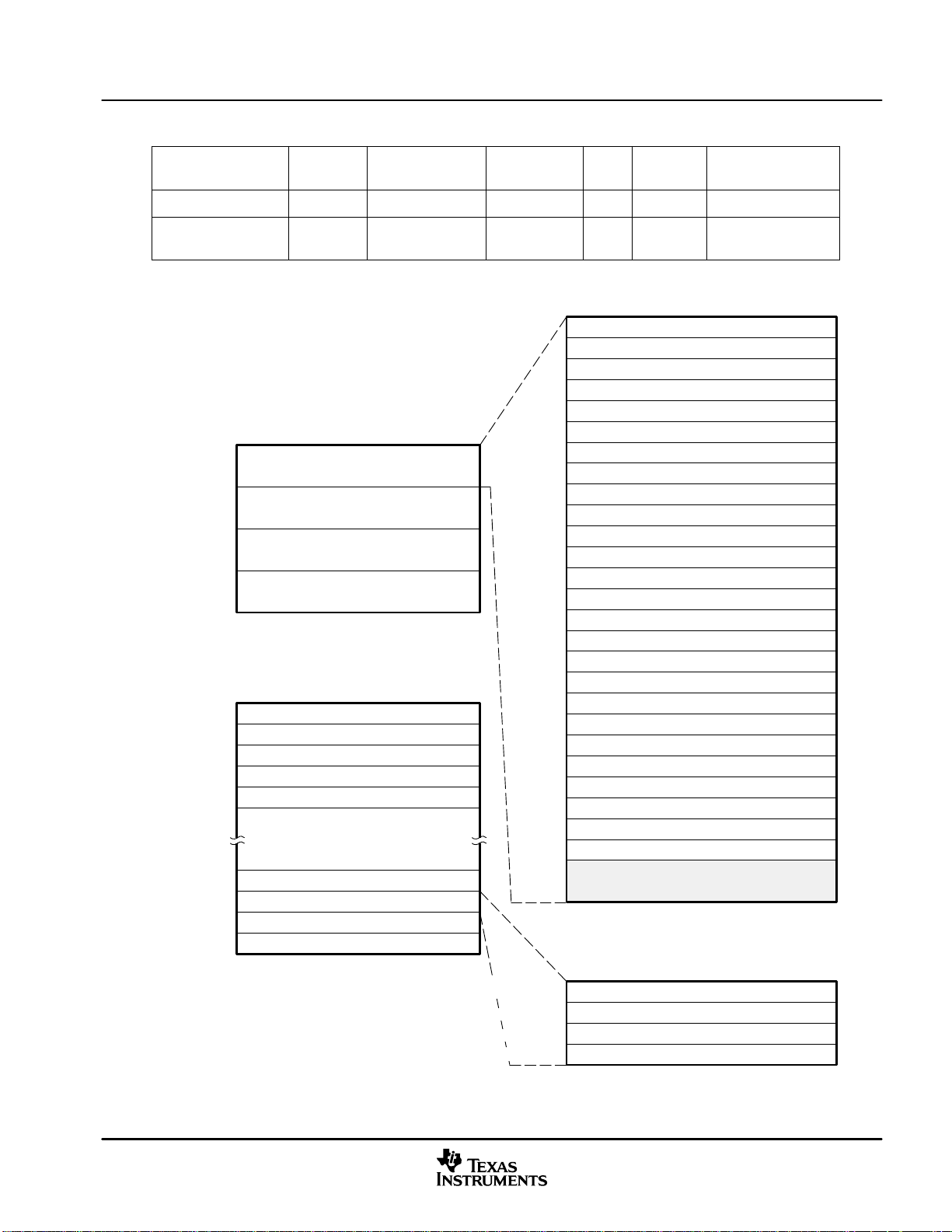
Table 4−5. 3.3-V eCAN Transceivers for the TMS320R281x DSPs (Continued)
ADVANCE INFORMATION
Peripherals
PART NUMBER SUPPLY
SN65HVD234 3.3 V Standby & Sleep Adjustable None −− −40°C to 125°C
SN65HVD235 3.3 V Standby Adjustable None Autobaud
6000h
603Fh
6040h
607Fh
6080h
60BFh
60C0h
60FFh
6100h−6107h
6108h−610Fh
6110h−6117h
6118h−611Fh
6120h−6127h
Message Object Time Stamps (MOTS)
VOLTAGE
eCAN Memory (512 Bytes)
Control and Status Registers
Local Acceptance Masks (LAM)
(32 × 32-Bit RAM)
(32 × 32-Bit RAM)
Message Object Time-Out (MOTO)
(32 × 32-Bit RAM)
eCAN Memory RAM (512 Bytes)
Mailbox 0
Mailbox 1
Mailbox 2
Mailbox 3
Mailbox 4
LOW-POWER
MODE
SLOPE
CONTROL
VREF OTHER T
−40°C to 125°C
Loopback
eCAN Control and Status Registers
Mailbox Enable − CANME
Mailbox Direction − CANMD
Transmission Request Set − CANTRS
Transmission Request Reset − CANTRR
Transmission Acknowledge − CANTA
Abort Acknowledge − CANAA
Received Message Pending − CANRMP
Received Message Lost − CANRML
Remote Frame Pending − CANRFP
Global Acceptance Mask − CANGAM
Master Control − CANMC
Bit-Timing Configuration − CANBTC
Error and Status − CANES
Transmit Error Counter − CANTEC
Receive Error Counter − CANREC
Global Interrupt Flag 0 − CANGIF0
Global Interrupt Mask − CANGIM
Global Interrupt Flag 1 − CANGIF1
Mailbox Interrupt Mask − CANMIM
Mailbox Interrupt Level − CANMIL
Overwrite Protection Control − CANOPC
TX I/O Control − CANTIOC
RX I/O Control − CANRIOC
Time Stamp Counter − CANTSC
Time-Out Control − CANTOC
Time-Out Status − CANTOS
A
61E0h−61E7h
61E8h−61EFh
61F0h−61F7h
61F8h−61FFh
Mailbox 28
Mailbox 29
Mailbox 30
Mailbox 31
61E8h−61E9h
61EAh−61EBh
61ECh−61EDh
61EEh−61EFh
Reserved
Message Mailbox (16 Bytes)
Message Identifier − MSGID
Message Control − MSGCTRL
Message Data Low − MDL
Message Data High − MDH
Figure 4−8. eCAN Memory Map
June 2004 SPRS257
65

Peripherals
ADVANCE INFORMATION
The CAN registers listed in Table 4−6 are used by the CPU to configure and control the CAN controller and
the message objects. eCAN control registers only support 32-bit read/write operations. Mailbox RAM can be
accessed as 16 bits or 32 bits. 32-bit accesses are aligned to an even boundary.
REGISTER NAME
CANME 0x00 6000 1 Mailbox enable
CANMD 0x00 6002 1 Mailbox direction
CANTRS 0x00 6004 1 Transmit request set
CANTRR 0x00 6006 1 Transmit request reset
CANTA 0x00 6008 1 Transmission acknowledge
CANAA 0x00 600A 1 Abort acknowledge
CANRMP 0x00 600C 1 Receive message pending
CANRML 0x00 600E 1 Receive message lost
CANRFP 0x00 6010 1 Remote frame pending
CANGAM 0x00 6012 1 Global acceptance mask
CANMC 0x00 6014 1 Master control
CANBTC 0x00 6016 1 Bit-timing configuration
CANES 0x00 6018 1 Error and status
CANTEC 0x00 601A 1 Transmit error counter
CANREC 0x00 601C 1 Receive error counter
CANGIF0 0x00 601E 1 Global interrupt flag 0
CANGIM 0x00 6020 1 Global interrupt mask
CANGIF1 0x00 6022 1 Global interrupt flag 1
CANMIM 0x00 6024 1 Mailbox interrupt mask
CANMIL 0x00 6026 1 Mailbox interrupt level
CANOPC 0x00 6028 1 Overwrite protection control
CANTIOC 0x00 602A 1 TX I/O control
CANRIOC 0x00 602C 1 RX I/O control
CANTSC 0x00 602E 1 Time stamp counter (Reserved in SCC mode)
CANTOC 0x00 6030 1 Time-out control (Reserved in SCC mode)
CANTOS 0x00 6032 1 Time-out status (Reserved in SCC mode)
†
These registers are mapped to Peripheral Frame 1.
ADDRESS
Table 4−6. CAN Registers Map
SIZE
(x32)
†
DESCRIPTION
66
June 2004SPRS257

4.5 Multichannel Buffered Serial Port (McBSP) Module
ADVANCE INFORMATION
The McBSP module has the following features:
• Compatible to McBSP in TMS320C54x /TMS320C55x DSP devices, except the DMA features
• Full-duplex communication
• Double-buffered data registers which allow a continuous data stream
• Independent framing and clocking for receive and transmit
• External shift clock generation or an internal programmable frequency shift clock
• A wide selection of data sizes including 8-, 12-, 16-, 20-, 24-, or 32-bits
• 8-bit data transfers with LSB or MSB first
• Programmable polarity for both frame synchronization and data clocks
• HIghly programmable internal clock and frame generation
• Support A-bis mode
• Direct interface to industry-standard CODECs, Analog Interface Chips (AICs), and other serially
connected A/D and D/A devices
• Works with SPI-compatible devices
Peripherals
• Two 16 x 16-level FIFO for Transmit channel
• Two 16 x 16-level FIFO for Receive channel
The following application interfaces can be supported on the McBSP:
• T1/E1 framers
• MVIP switching-compatible and ST-BUS-compliant devices including:
− MVIP framers
− H.100 framers
− SCSA framers
− IOM-2 compliant devices
− AC97-compliant devices (the necessary multiphase frame synchronization capability is provided.)
− IIS-compliant devices
• McBSP clock rate = CLKG =
Serial port performance is limited by I/O buffer switching speed. Internal prescalers must be adjusted such
that the peripheral speed is less than the I/O buffer speed limit—20-MHz maximum.
Figure 4−9 shows the block diagram of the McBSP module with FIFO, interfaced to the R281x version of
Peripheral Frame 2.
CLKSRG
(1 ) CLKGDIV)
, where CLKSRG source could be LSPCLK, CLKX, or CLKR.
TMS320C54x and TMS320C55x are trademarks of Texas Instruments.
June 2004 SPRS257
67
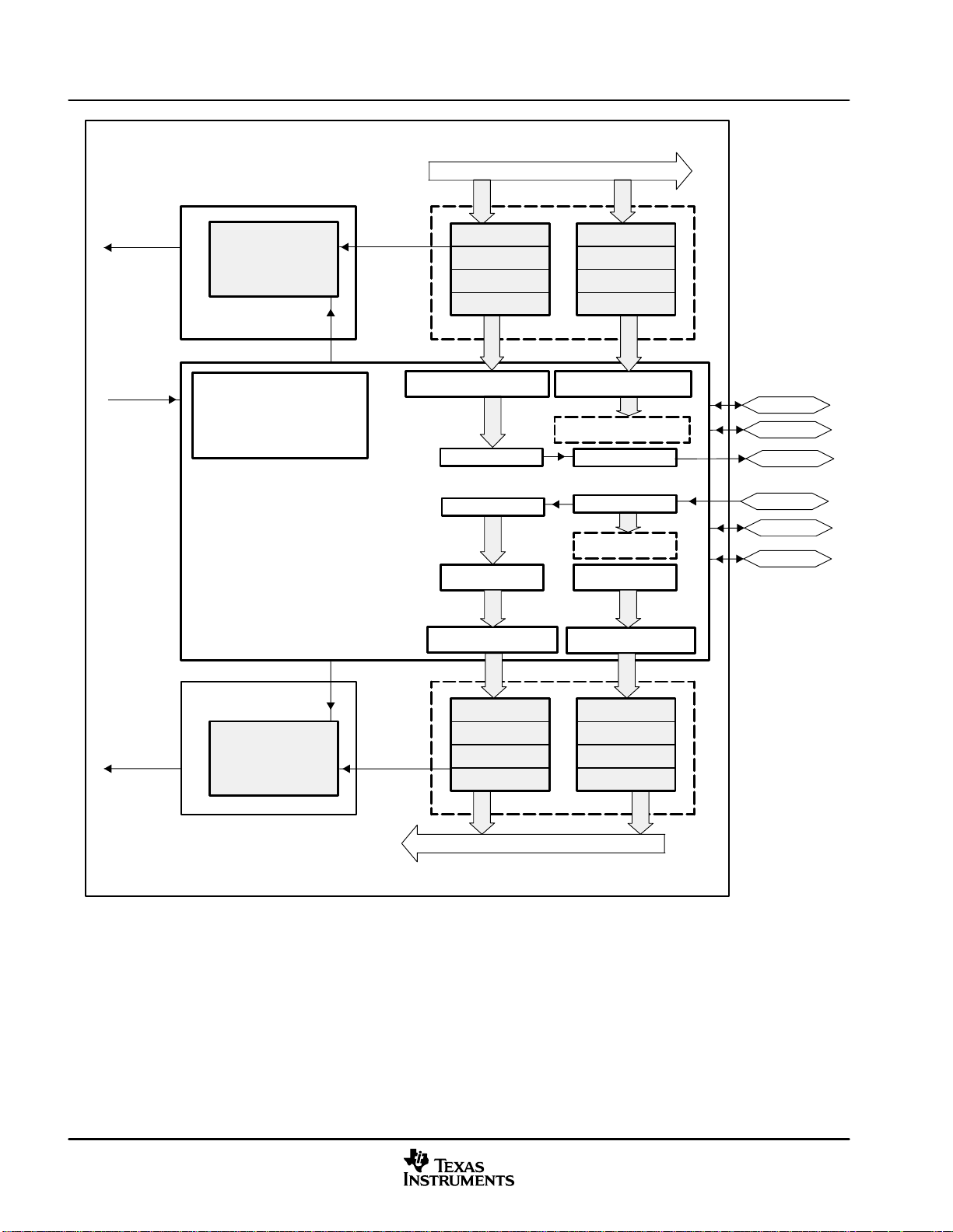
Peripherals
ADVANCE INFORMATION
Peripheral Write Bus
MXINT
To CPU
LSPCLK
MRINT
To CPU
TX Interrupt Logic
McBSP Transmit
Interrupt Select Logic
McBSP Registers
and Control Logic
McBSP
McBSP Receive
Interrupt Select Logic
RX Interrupt Logic
TX FIFO
Interrupt
RX FIFO
Interrupt
TX FIFO _15
—
TX FIFO _1
TX FIFO _0
TX FIFO Registers
16
DXR2 Transmit Buffer
16
XSR2
RSR2
16
16
DRR2 Receive Buffer
16
RX FIFO _15
—
RX FIFO _1
RX FIFO _0
RX FIFO Registers
TX FIFO _15
—
TX FIFO _1
TX FIFO _0
16
DXR1 Transmit Buffer
16
Compand Logic
XSR1
RSR1
16
Expand Logic
RBR1 RegisterRBR2 Register
16
DRR1 Receive Buffer
16
RX FIFO _15
—
RX FIFO _1
RX FIFO _0
FSX
CLKX
DX
DR
CLKR
FSR
68
Peripheral Read Bus
Figure 4−9. McBSP Module With FIFO
June 2004SPRS257

Table 4−7 provides a summary of the McBSP registers.
ADVANCE INFORMATION
Table 4−7. McBSP Register Summary
Peripherals
NAME
− − − 0x0000 McBSP Receive Buffer Register
− − − 0x0000 McBSP Receive Shift Register
− − − 0x0000 McBSP Transmit Shift Register
DRR2 00 R 0x0000
DRR1 01 R 0x0000
DXR2 02 W 0x0000
DXR1 03 W 0x0000
SPCR2 04 R/W 0x0000 McBSP Serial Port Control Register 2
SPCR1 05 R/W 0x0000 McBSP Serial Port Control Register 1
RCR2 06 R/W 0x0000 McBSP Receive Control Register 2
RCR1 07 R/W 0x0000 McBSP Receive Control Register 1
XCR2 08 R/W 0x0000 McBSP Transmit Control Register 2
XCR1 09 R/W 0x0000 McBSP Transmit Control Register 1
SRGR2 0A R/W 0x0000 McBSP Sample Rate Generator Register 2
SRGR1 0B R/W 0x0000 McBSP Sample Rate Generator Register 1
MCR2 0C R/W 0x0000 McBSP Multichannel Register 2
MCR1 0D R/W 0x0000 McBSP Multichannel Register 1
RCERA 0E R/W 0x0000 McBSP Receive Channel Enable Register Partition A
RCERB 0F R/W 0x0000 McBSP Receive Channel Enable Register Partition B
XCERA 10 R/W 0x0000 McBSP Transmit Channel Enable Register Partition A
XCERB 11 R/W 0x0000 McBSP Transmit Channel Enable Register Partition B
PCR1 12 R/W 0x0000 McBSP Pin Control Register
RCERC 13 R/W 0x0000 McBSP Receive Channel Enable Register Partition C
RCERD 14 R/W 0x0000 McBSP Receive Channel Enable Register Partition D
XCERC 15 R/W 0x0000 McBSP Transmit Channel Enable Register Partition C
XCERD 16 R/W 0x0000 McBSP Transmit Channel Enable Register Partition D
†
DRR2/DRR1 and DXR2/DXR1 share the same addresses of receive and transmit FIFO registers in FIFO mode.
‡
FIFO pointers advancing is based on order of access to DRR2/DRR1 and DXR2/DXR1 registers.
ADDRESS
0x00 78xxh
TYPE
(R/W)
DATA REGISTERS, RECEIVE, TRANSMIT
McBSP CONTROL REGISTERS
MULTICHANNEL CONTROL REGISTERS
RESET VALUE
(HEX)
McBSP Data Receive Register 2
− Read First if the word size is greater than 16 bits,
else ignore DRR2
McBSP Data Receive Register 1
− Read Second if the word size is greater than 16 bits,
else read DRR1 only
McBSP Data Transmit Register 2
− Write First if the word size is greater than 16 bits,
else ignore DXR2
McBSP Data Transmit Register 1
− Write Second if the word size is greater than 16 bits,
else write to DXR1 only
DESCRIPTION
†
June 2004 SPRS257
69

Peripherals
ADVANCE INFORMATION
Table 4−7. McBSP Register Summary (Continued)
NAME
RCERE 17 R/W 0x0000 McBSP Receive Channel Enable Register Partition E
RCERF 18 R/W 0x0000 McBSP Receive Channel Enable Register Partition F
XCERE 19 R/W 0x0000 McBSP Transmit Channel Enable Register Partition E
XCERF 1A R/W 0x0000 McBSP Transmit Channel Enable Register Partition F
RCERG 1B R/W 0x0000 McBSP Receive Channel Enable Register Partition G
RCERH 1C R/W 0x0000 McBSP Receive Channel Enable Register Partition H
XCERG 1D R/W 0x0000 McBSP Transmit Channel Enable Register Partition G
XCERH 1E R/W 0x0000 McBSP Transmit Channel Enable Register Partition H
DRR2 00 R 0x0000
DRR1 01 R 0x0000
DXR2 02 W 0x0000
DXR1 03 W 0x0000
MFFTX 20 R/W 0xA000 McBSP Transmit FIFO Register
MFFRX 21 R/W 0x201F McBSP Receive FIFO Register
MFFCT 22 R/W 0x0000 McBSP FIFO Control Register
MFFINT 23 R/W 0x0000 McBSP FIFO Interrupt Register
MFFST 24 R/W 0x0000 McBSP FIFO Status Register
†
DRR2/DRR1 and DXR2/DXR1 share the same addresses of receive and transmit FIFO registers in FIFO mode.
‡
FIFO pointers advancing is based on order of access to DRR2/DRR1 and DXR2/DXR1 registers.
ADDRESS
0x00 78xxh
TYPE
(R/W)
MULTICHANNEL CONTROL REGISTERS (CONTINUED)
FIFO MODE REGISTERS (applicable only in FIFO mode)
RESET VALUE
(HEX)
FIFO Data Registers
FIFO Control Registers
‡
McBSP Data Receive Register 2 − Top of receive FIFO
− Read First FIFO pointers will not advance
McBSP Data Receive Register 1 − Top of receive FIFO
− Read Second for FIFO pointers to advance
McBSP Data Transmit Register 2 − Top of transmit FIFO
− Write First FIFO pointers will not advance
McBSP Data Transmit Register 1 − Top of transmit FIFO
− Write Second for FIFO pointers to advance
DESCRIPTION
4.6 Serial Communications Interface (SCI) Module
70
R281x devices include two serial communications interface (SCI) modules. The SCI modules support digital
communications between the CPU and other asynchronous peripherals that use the standard
non-return-to-zero (NRZ) format. The SCI receiver and transmitter are double-buffered, and each has its own
separate enable and interrupt bits. Both can be operated independently or simultaneously in the full-duplex
mode. To ensure data integrity, the SCI checks received data for break detection, parity, overrun, and framing
errors. The bit rate is programmable to over 65000 different speeds through a 16-bit baud-select register.
Features of each SCI module include:
• Two external pins:
− SCITXD: SCI transmit-output pin
− SCIRXD: SCI receive-input pin
NOTE: Both pins can be used as GPIO if not used for SCI.
June 2004SPRS257

• Baud rate programmable to 64K different rates
ADVANCE INFORMATION
Peripherals
− Baud rate =
Serial port performance is limited by I/O buffer switching speed. Internal prescalers must be adjusted such
that the peripheral speed is less than the I/O buffer speed limit—20 MHz maximum.
• Data-word format
− One start bit
− Data-word length programmable from one to eight bits
− Optional even/odd/no parity bit
− One or two stop bits
• Four error-detection flags: parity, overrun, framing, and break detection
• Two wake-up multiprocessor modes: idle-line and address bit
• Half- or full-duplex operation
• Double-buffered receive and transmit functions
• Transmitter and receiver operations can be accomplished through interrupt-driven or polled algorithms
with status flags.
− Transmitter: TXRDY flag (transmitter-buffer register is ready to receive another character) and
TX EMPTY flag (transmitter-shift register is empty)
LSPCLK
(BRR ) 1) * 8
LSPCLK
=
16
, when BRR ≠ 0
, when BRR = 0
− Receiver: RXRDY flag (receiver-buffer register is ready to receive another character), BRKDT flag
(break condition occurred), and RX ERROR flag (monitoring four interrupt conditions)
• Separate enable bits for transmitter and receiver interrupts (except BRKDT)
• Max bit rate +
• NRZ (non-return-to-zero) format
• Ten SCI module control registers located in the control register frame beginning at address 7050h
All registers in this module are 8-bit registers that are connected to Peripheral Frame 2. When a register is
accessed, the register data is in the lower byte (7−0), and the upper byte (15 − 8) is read as zeros. Writing
to the upper byte has no effect.
Enhanced features:
• Auto baud-detect hardware logic
• 16-level transmit/receive FIFO
150 MHz
2 8
+ 9.375 106bńs
June 2004 SPRS257
71
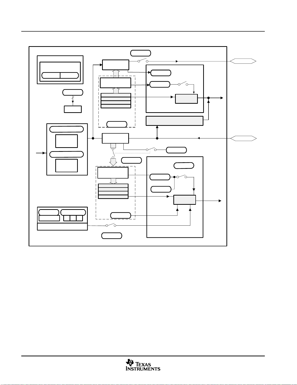
Peripherals
ADVANCE INFORMATION
Figure 4−10 shows the SCI module block diagram.
LSPCLK
Frame Format and Mode
Parity
Even/Odd Enable
SCICCR.6 SCICCR.5
TXWAKE
SCICTL1.3
1
WUT
SCIHBAUD. 15 − 8
Baud Rate
MSbyte
Register
SCILBAUD. 7 − 0
Baud Rate
LSbyte
Register
SCIRXST.7
SCIRXST.4 − 2
RX Error
RX Error
SCICTL1.1
TXSHF
Register
8
Transmitter−Data
Buffer Register
8
TX FIFO _0
TX FIFO _1
−−−−−
TX FIFO _15
SCITXBUF.7−0
TX FIFO registers
SCIFFENA
SCIFFTX.14
RXSHF
Register
TXENA
TX FIFO
Interrupts
SCITXD
TX EMPTY
SCICTL2.6
TXRDY
SCICTL2.7
TX INT ENA
SCICTL2.0
TX Interrupt
Logic
SCI TX Interrupt select logic
AutoBaud Detect logic
SCIRXD
TXINT
To CPU
SCITXD
SCIRXD
RXWAKE
SCIRXST.1
RXENA
SCICTL1.0
8
Receive Data
Buffer register
SCIRXBUF.7−0
8
RX FIFO _15
−−−−−
RX FIFO_1
RX FIFO _0
SCIRXBUF.7−0
RX FIFO registers
RX FIFO
Interrupts
RXRDY
SCIRXST.6
BRKDT
SCIRXST.5
SCICTL2.1
RX/BK INT ENA
RX Interrupt
Logic
RXINT
To CPU
RXFFOVF
PEFE OE
SCIFFRX.15
RX ERR INT ENA
SCICTL1.6
SCI RX Interrupt select logic
72
Figure 4−10. Serial Communications Interface (SCI) Module Block Diagram
June 2004SPRS257
Peripherals
ADVANCE INFORMATION
The SCI port operation is configured and controlled by the registers listed in Table 4−8 and Table 4−9.
Table 4−8. SCI-A Registers
NAME
SCICCRA 0x00 7050 1 SCI-A Communications Control Register
SCICTL1A 0x00 7051 1 SCI-A Control Register 1
SCIHBAUDA 0x00 7052 1 SCI-A Baud Register, High Bits
SCILBAUDA 0x00 7053 1 SCI-A Baud Register, Low Bits
SCICTL2A 0x00 7054 1 SCI-A Control Register 2
SCIRXSTA 0x00 7055 1 SCI-A Receive Status Register
SCIRXEMUA 0x00 7056 1 SCI-A Receive Emulation Data Buffer Register
SCIRXBUFA 0x00 7057 1 SCI-A Receive Data Buffer Register
SCITXBUFA 0x00 7059 1 SCI-A Transmit Data Buffer Register
SCIFFTXA 0x00 705A 1 SCI-A FIFO Transmit Register
SCIFFRXA 0x00 705B 1 SCI-A FIFO Receive Register
SCIFFCTA 0x00 705C 1 SCI-A FIFO Control Register
SCIPRIA 0x00 705F 1 SCI-A Priority Control Register
†
Shaded registers are new registers for the FIFO mode.
ADDRESS SIZE (x16) DESCRIPTION
Table 4−9. SCI-B Registers
NAME
SCICCRB 0x00 7750 1 SCI-B Communications Control Register
SCICTL1B 0x00 7751 1 SCI-B Control Register 1
SCIHBAUDB 0x00 7752 1 SCI-B Baud Register, High Bits
SCILBAUDB 0x00 7753 1 SCI-B Baud Register, Low Bits
SCICTL2B 0x00 7754 1 SCI-B Control Register 2
SCIRXSTB 0x00 7755 1 SCI-B Receive Status Register
SCIRXEMUB 0x00 7756 1 SCI-B Receive Emulation Data Buffer Register
SCIRXBUFB 0x00 7757 1 SCI-B Receive Data Buffer Register
SCITXBUFB 0x00 7759 1 SCI-B Transmit Data Buffer Register
SCIFFTXB 0x00 775A 1 SCI-B FIFO Transmit Register
SCIFFRXB 0x00 775B 1 SCI-B FIFO Receive Register
SCIFFCTB 0x00 775C 1 SCI-B FIFO Control Register
SCIPRIB 0x00 775F 1 SCI-B Priority Control Register
ADDRESS SIZE (x16) DESCRIPTION
†
†‡
†
Shaded registers are new registers for the FIFO mode.
‡
Registers in this table are mapped to peripheral bus 16 space. This space only allows 16-bit accesses. 32-bit accesses produce undefined results.
4.7 Serial Peripheral Interface (SPI) Module
R281x devices include the four-pin serial peripheral interface (SPI) module. The SPI is a high-speed,
synchronous serial I/O port that allows a serial bit stream of programmed length (one to sixteen bits) to be
shifted into and out of the device at a programmable bit-transfer rate. Normally, the SPI is used for
communications between the DSP controller and external peripherals or another processor. Typical
applications include external I/O or peripheral expansion through devices such as shift registers, display
drivers, and ADCs. Multidevice communications are supported by the master/slave operation of the SPI.
June 2004 SPRS257
73

Peripherals
ADVANCE INFORMATION
The SPI module features include:
• Four external pins:
− SPISOMI: SPI slave-output/master-input pin
− SPISIMO: SPI slave-input/master-output pin
− SPISTE
− SPICLK: SPI serial-clock pin
NOTE: All four pins can be used as GPIO, if the SPI module is not used.
• Two operational modes: master and slave
• Baud rate: 125 different programmable rates
− Baud rate =
Serial port performance is limited by I/O buffer switching speed. Internal prescalers must be adjusted
such that the peripheral speed is less than the I/O buffer speed limit—20 MHz maximum.
• Data word length: one to sixteen data bits
• Four clocking schemes (controlled by clock polarity and clock phase bits) include:
− Falling edge without phase delay: SPICLK active-high. SPI transmits data on the falling edge of the
SPICLK signal and receives data on the rising edge of the SPICLK signal.
− Falling edge with phase delay: SPICLK active-high. SPI transmits data one half-cycle ahead of the
falling edge of the SPICLK signal and receives data on the falling edge of the SPICLK signal.
− Rising edge without phase delay: SPICLK inactive-low. SPI transmits data on the rising edge of the
SPICLK signal and receives data on the falling edge of the SPICLK signal.
: SPI slave transmit-enable pin
LSPCLK
(SPIBRR ) 1)
LSPCLK
=
4
, when BRR ≠ 0
, when BRR = 0, 1, 2, 3
− Rising edge with phase delay: SPICLK inactive-low. SPI transmits data one half-cycle ahead of the
falling edge of the SPICLK signal and receives data on the rising edge of the SPICLK signal.
• Simultaneous receive and transmit operation (transmit function can be disabled in software)
• Transmitter and receiver operations are accomplished through either interrupt-driven or polled
algorithms.
• Nine SPI module control registers: Located in control register frame beginning at address 7040h.
All registers in this module are 16-bit registers that are connected to Peripheral Frame 2. When a register
is accessed, the register data is in the lower byte (7 −0), and the upper byte (15 −8) is read as zeros. Writing
to the upper byte has no effect.
Enhanced feature:
• 16-level transmit/receive FIFO
• Delayed transmit control
74
June 2004SPRS257

Peripherals
ADVANCE INFORMATION
The SPI port operation is configured and controlled by the registers listed in Table 4−10.
Table 4−10. SPI Registers
NAME ADDRESS SIZE (x16) DESCRIPTION
SPICCR 0x00 7040 1 SPI Configuration Control Register
SPICTL 0x00 7041 1 SPI Operation Control Register
SPISTS 0x00 7042 1 SPI Status Register
SPIBRR 0x00 7044 1 SPI Baud Rate Register
SPIRXEMU 0x00 7046 1 SPI Receive Emulation Buffer Register
SPIRXBUF 0x00 7047 1 SPI Serial Input Buffer Register
SPITXBUF 0x00 7048 1 SPI Serial Output Buffer Register
SPIDAT 0x00 7049 1 SPI Serial Data Register
SPIFFTX 0x00 704A 1 SPI FIFO Transmit Register
SPIFFRX 0x00 704B 1 SPI FIFO Receive Register
SPIFFCT 0x00 704C 1 SPI FIFO Control Register
SPIPRI 0x00 704F 1 SPI Priority Control Register
NOTE: The registers in this table are mapped to Peripheral Frame 2. This space only allows 16-bit accesses. 32-bit accesses produce undefined
results.
June 2004 SPRS257
75

Peripherals
ADVANCE INFORMATION
Figure 4−11 is a block diagram of the SPI in slave mode.
SPIFFTX.14
RX FIFO registers
SPIRXBUF
RX FIFO _0
RX FIFO _1
−−−−−
RX FIFO _15
SPIRXBUF
Buffer Register
16
Data Register
SPIDAT.15 − 0
SPI Char
LSPCLK
SPIFFENA
16
TX FIFO registers
SPITXBUF
TX FIFO _15
−−−−−
TX FIFO _1
TX FIFO _0
16
SPITXBUF
Buffer Register
16
SPIDAT
Talk
SPICTL.1
State Control
SPICCR.3 − 0
SPI Bit Rate
SPIBRR.6 − 0
4561230
RX FIFO Interrupt
TX FIFO Interrupt
0123
M
S
M
S
S
M
Receiver
Overrun Flag
SPISTS.7
SPIFFOVF FLAG
SPIFFRX.15
SPI INT FLAG
SPISTS.6
SW1
SW2
S
M
Overrun
INT ENA
SPICTL.4
RX Interrupt
Logic
TX Interrupt
Logic
SPI INT
ENA
SPICTL.0
M
S
M
S
Master/Slave
SPICTL.2
SW3
Clock
Polarity
SPICCR.6 SPICTL.3
SPIINT/SPIRXINT
To CPU
SPITXINT
Clock
Phase
SPISIMO
SPISOMI
SPISTE
SPICLK
†
†
76
SPISTE is driven low by the master for a slave device.
Figure 4−11. Serial Peripheral Interface Module Block Diagram (Slave Mode)
June 2004SPRS257

4.8 GPIO MUX
ADVANCE INFORMATION
The GPIO Mux registers, are used to select the operation of shared pins on R281x devices. The pins can be
individually selected to operate as “Digital I/O” or connected to “Peripheral I/O” signals (via the GPxMUX
registers). If selected for “Digital I/O” mode, registers are provided to configure the pin direction (via the
GPxDIR registers) and to qualify the input signal to remove unwanted noise (via the GPxQUAL) registers).
Table 4−11 lists the GPIO Mux Registers.
Peripherals
Table 4−11. GPIO Mux Registers
NAME
GPAMUX 0x00 70C0 1 GPIO A Mux Control Register
GPADIR 0x00 70C1 1 GPIO A Direction Control Register
GPAQUAL 0x00 70C2 1 GPIO A Input Qualification Control Register
reserved 0x00 70C3 1
GPBMUX 0x00 70C4 1 GPIO B Mux Control Register
GPBDIR 0x00 70C5 1 GPIO B Direction Control Register
GPBQUAL 0x00 70C6 1 GPIO B Input Qualification Control Register
reserved 0x00 70C7 1
reserved 0x00 70C8 1
reserved 0x00 70C9 1
reserved 0x00 70CA 1
reserved 0x00 70CB 1
GPDMUX 0x00 70CC 1 GPIO D Mux Control Register
GPDDIR 0x00 70CD 1 GPIO D Direction Control Register
GPDQUAL 0x00 70CE 1 GPIO D Input Qualification Control Register
reserved 0x00 70CF 1
GPEMUX 0x00 70D0 1 GPIO E Mux Control Register
GPEDIR 0x00 70D1 1 GPIO E Direction Control Register
GPEQUAL 0x00 70D2 1 GPIO E Input Qualification Control Register
reserved 0x00 70D3 1
GPFMUX 0x00 70D4 1 GPIO F Mux Control Register
GPFDIR 0x00 70D5 1 GPIO F Direction Control Register
reserved 0x00 70D6 1
reserved 0x00 70D7 1
GPGMUX 0x00 70D8 1 GPIO G Mux Control Register
GPGDIR 0x00 70D9 1 GPIO G Direction Control Register
reserved 0x00 70DA 1
reserved 0x00 70DB 1
reserved
†
Reserved locations will return undefined values and writes will be ignored.
‡
Not all inputs will support input signal qualification.
§
These registers are EALLOW protected. This prevents spurious writes from overwriting the contents and corrupting the system.
ADDRESS SIZE (x16) REGISTER DESCRIPTION
0x00 70DC
0x00 70DF
4
†‡§
June 2004 SPRS257
77

Peripherals
ADVANCE INFORMATION
If configured for digital I/O mode, additional registers are provided for setting individual I/O signals (via the
GPxSET registers), for clearing individual I/O signals (via the GPxCLEAR registers), for toggling individual I/O
signals (via the GPxTOGGLE registers), or for reading/writing to the individual I/O signals (via the GPxDAT
registers). Table 4−12 lists the GPIO Data Registers. For more information, see the TMS320F28x System
Control and Interrupts Reference Guide (literature number SPRU078).
†
‡
Table 4−12. GPIO Data Registers
NAME
GPADAT 0x00 70E0 1 GPIO A Data Register
GPASET 0x00 70E1 1 GPIO A Set Register
GPACLEAR 0x00 70E2 1 GPIO A Clear Register
GPATOGGLE 0x00 70E3 1 GPIO A Toggle Register
GPBDAT 0x00 70E4 1 GPIO B Data Register
GPBSET 0x00 70E5 1 GPIO B Set Register
GPBCLEAR 0x00 70E6 1 GPIO B Clear Register
GPBTOGGLE 0x00 70E7 1 GPIO B Toggle Register
reserved 0x00 70E8 1
reserved 0x00 70E9 1
reserved 0x00 70EA 1
reserved 0x00 70EB 1
GPDDAT 0x00 70EC 1 GPIO D Data Register
GPDSET 0x00 70ED 1 GPIO D Set Register
GPDCLEAR 0x00 70EE 1 GPIO D Clear Register
GPDTOGGLE 0x00 70EF 1 GPIO D Toggle Register
GPEDAT 0x00 70F0 1 GPIO E Data Register
GPESET 0x00 70F1 1 GPIO E Set Register
GPECLEAR 0x00 70F2 1 GPIO E Clear Register
GPETOGGLE 0x00 70F3 1 GPIO E Toggle Register
GPFDAT 0x00 70F4 1 GPIO F Data Register
GPFSET 0x00 70F5 1 GPIO F Set Register
GPFCLEAR 0x00 70F6 1 GPIO F Clear Register
GPFTOGGLE 0x00 70F7 1 GPIO F Toggle Register
GPGDAT 0x00 70F8 1 GPIO G Data Register
GPGSET 0x00 70F9 1 GPIO G Set Register
GPGCLEAR 0x00 70FA 1 GPIO G Clear Register
GPGTOGGLE 0x00 70FB 1 GPIO G Toggle Register
reserved
Reserved locations will return undefined values and writes will be ignored.
These registers are NOT EALLOW protected. The above registers will typically be accessed regularly by the user.
ADDRESS SIZE (x16) REGISTER DESCRIPTION
0x00 70FC
0x00 70FF
4
†‡
78
June 2004SPRS257

Figure 4−12 shows how the various register bits select the various modes of operation.
ADVANCE INFORMATION
Peripherals
GPxDAT/SET/CLEAR/TOGGLE
GPxQUAL
Register
Register Bit(s)
01
Input Qualification
MUX
Digital I/O
GPxMUX
Register Bit
High-Impedance
Enable (1)
GPxDIR
Register Bit
MUX
Peripheral I/O
High-
Impedance
Control
10
SYSCLKOUT
XRS
Internal (Pullup or Pulldown)
PIN
NOTES: A. In the GPIO mode, when the GPIO pin is configured for output operation, reading the GPxDAT data register only gives the value
written, not the value at the pin. In the peripheral mode, the state of the pin can be read through the GPxDAT register, provided the
corresponding direction bit is zero (input mode).
B. Some selected input signals are qualified by the SYSCLKOUT. The GPxQUAL register specifies the qualification sampling period.
The sampling window is 6 samples wide and the output is only changed when all samples are the same (all 0’s or all 1’s). This feature
removes unwanted spikes from the input signal.
Figure 4−12. Modes of Operation
NOTE:
The input function of the GPIO pin and the input path to the peripheral are always enabled.
It is the output function of the GPIO pin that is multiplexed with the output path of the primary
(peripheral) function. Since the output buffer of a pin connects back to the input buffer, any
GPIO signal present at the pin will be propagated to the peripheral module as well. Therefore,
when a pin is configured for GPIO operation, the corresponding peripheral functionality (and
interrupt-generating capability) must be disabled. Otherwise, interrupts may be inadvertently
triggered. This is especially critical when the PDPINTA
pins, since a value of zero for GPDDAT.0 or GPDDAT.5 (PDPINTx
high-impedance state. The CxTRIP
and TxCTRIP pins will also put the corresponding PWM
and PDPINTB pins are used as GPIO
) will put PWM pins in a
pins in high impedance, if they are driven low (as GPIO pins) and bit EXTCONx.0 = 1.
June 2004 SPRS257
79

Development Support
ADVANCE INFORMATION
5 Development Support
Texas Instruments (TI) offers an extensive line of development tools for the C28x generation of DSPs,
including tools to evaluate the performance of the processors, generate code, develop algorithm
implementations, and fully integrate and debug software and hardware modules.
The following products support development of R281x-based applications:
Software Development Tools
• Code Composer Studio Integrated Development Environment (IDE)
− C/C++ Compiler
− Code generation tools
− Assembler/Linker
− Cycle Accurate Simulator
• Application algorithms
• Sample applications code
Hardware Development Tools
• R2812 eZdsp
5.1 Device and Development Support Tool Nomenclature
• JTAG-based emulators − SPI515, XDS510PP, XDS510PP Plus, XDS510 USB
• Universal 5-V dc power supply
• Documentation and cables
To designate the stages in the product development cycle, TI assigns prefixes to the part numbers of all
[TMS320] DSP devices and support tools. Each [TMS320] DSP commercial family member has one of three
prefixes: TMX, TMP, or TMS (e.g., TMS320R2812GHH). Texas Instruments recommends two of three
possible prefix designators for its support tools: TMDX and TMDS. These prefixes represent evolutionary
stages of product development from engineering prototypes (TMX/ TMDX) through fully qualified production
devices/tools (TMS/TMDS).
TMX Experimental device that is not necessarily representative of the final device’s electrical specifications
TMP Final silicon die that conforms to the device’s electrical specifications but has not completed quality
and reliability verification
TMS Fully qualified production device
Support tool development evolutionary flow:
TMDX Development-support product that has not yet completed Texas Instruments internal qualification
testing.
TMDS Fully qualified development-support product
TMX and TMP devices and TMDX development−support tools are shipped against the following disclaimer:
“Developmental product is intended for internal evaluation purposes.“
TMS devices and TMDS development-support tools have been characterized fully, and the quality and
reliability of the device have been demonstrated fully. TI’s standard warranty applies.
TMS320 is a trademark of Texas Instruments.
80
June 2004SPRS257

Development Support
ADVANCE INFORMATION
Predictions show that prototype devices (TMX or TMP) have a greater failure rate than the standard
production devices. Texas Instruments recommends that these devices not be used in any production system
because their expected end-use failure rate still is undefined. Only qualified production devices are to be used.
TI device nomenclature also includes a suffix with the device family name. This suffix indicates the package
type (for example, PBK) and temperature range (for example, A). Figure 5−1 provides a legend for reading
the complete device name for any TMS320x28x family member.
PREFIX
TMX = experimental device
TMP = prototype device
TMS = qualified device
DEVICE FAMILY
320 = TMS320
TECHNOLOGY
F = Flash EEPROM (1.8-V/1.9-V Core/3.3-V I/O)
C = ROM (1.8-V/1.9-V Core/3.3-V I/O)
R = RAM only (1.8-V/1.9-V Core/3.3-V I/O)
†
BGA = Ball Grid Array
LQFP = Low-Profile Quad Flatpack
Figure 5−1. TMS320x28x Device Nomenclature
5.2 Documentation Support
Extensive documentation supports all of the TMS320 DSP family generations of devices from product
announcement through applications development. The types of documentation available include: data sheets
and data manuals, with design specifications; and hardware and software applications. Useful reference
documentation includes:
TMS 320 R 2812 PBK
DSP Family
A
TEMPERATURE RANGE
A=−40°C to 85°C
S=−40°C to 125°C
Q=−40°C to 125°C − Q100
fault grading
PACKAGE TYPE
GHH = 179-ball MicroStar BGA
ZHH = 179-ball MicroStar BGA (lead-free)
PGF = 176-pin LQFP
PBK = 128-pin LQFP
DEVICE
2811
2812
†
TMS320C28x DSP CPU and Instruction Set Reference Guide (literature number SPRU430) describes the
central processing unit (CPU) and the assembly language instructions of the TMS320C28x fixed-point digital
signal processors (DSPs). It also describes emulation features available on these DSPs.
TMS320C28x Peripheral Reference Guide (literature number SPRU566) describes the peripheral reference
guides of the 28x digital signal processors (DSPs).
TMS320F28x Analog-to-Digital Converter (ADC) Reference Guide (literature number SPRU060)
describes the ADC module. The module is a 12−bit pipelined ADC. The analog circuits of this converter,
referred to as the core in this document, include the front-end analog multiplexers (MUXs), sample−and−hold
(S/H) circuits, the conversion core, voltage regulators, and other analog supporting circuits. Digital circuits,
referred to as the wrapper in this document, include programmable conversion sequencer, result registers,
interface to analog circuits, interface to device peripheral bus, and interface to other on-chip modules.
TMS320F28x Boot ROM Reference Guide (literature number SPRU095) describes the purpose and
features of the bootloader (factory-programmed boot-loading software). It also describes other contents of the
device on-chip boot ROM and identifies where all of the information is located within that memory.
June 2004 SPRS257
81

Development Support
ADVANCE INFORMATION
TMS320F28x Enhanced Controller Area Network (eCAN) Reference Guide (literature number SPRU074)
describes the eCAN that uses established protocol to communicate serially with other controllers in electrically
noisy environments. With 32 fully configurable mailboxes and time-stamping feature, the eCAN module
provides a versatile and robust serial communication interface. The eCAN module implemented in the C28x
DSP is compatible with the CAN 2.0B standard (active).
TMS320F28x Event Manager (EV) Reference Guide (literature number SPRU065) describes the EV
modules that provide a broad range of functions and features that are particularly useful in motion control and
motor control applications. The EV modules include general-purpose (GP) timers, full-compare/PWM units,
capture units, and quadrature-encoder pulse (QEP) circuits.
TMS320F28x External Interface (XINTF) Reference Guide (literature number SPRU067) describes the
external interface (XINTF) of the 28x digital signal processors (DSPs).
TMS320F28x Multichannel Buffered Serial Ports (McBSPs) Reference Guide (literature number
SPRU061) describes the McBSP) available on the C28x devices. The McBSPs allow direct interface between
a DSP and other devices in a system.
TMS320F28x Serial Communication Interface (SCI) Reference Guide (literature number SPRU051)
describes the SCI that is a two-wire asynchronous serial port, commonly known as a UART. The SCI modules
support digital communications between the CPU and other asynchronous peripherals that use the standard
non-return-to-zero (NRZ) format.
TMS320F28x Serial Peripheral Interface (SPI) Reference Guide (literature number SPRU059) describes
the SPI − a high-speed synchronous serial input/output (I/O) port that allows a serial bit stream of programmed
length (one to sixteen bits) to be shifted into and out of the device at a programmed bit−transfer rate. The SPI
is used for communications between the DSP controller and external peripherals or another controller.
TMS320F28x System Control and Interrupts Reference Guide (literature number SPRU078) describes
the various interrupts and system control features of the 28x digital signal processors (DSPs).
3.3 V DSP for Digital Motor Control Application Report (literature number SPRA550). New generations
of motor control digital signal processors (DSPs) lower their supply voltages from 5 V to 3.3 V to offer higher
performance at lower cost. Replacing traditional 5-V digital control circuitry by 3.3-V designs introduce no
additional system cost and no significant complication in interfacing with TTL and CMOS compatible
components, as well as with mixed voltage ICs such as power transistor gate drivers. Just like 5-V based
designs, good engineering practice should be exercised to minimize noise and EMI effects by proper
component layout and PCB design when 3.3-V DSP, ADC, and digital circuitry are used in a mixed signal
environment, with high and low voltage analog and switching signals, such as a motor control system. In
addition, software techniques such as Random PWM method can be used by special features of the Texas
Instruments (TI) TMS320x24xx DSP controllers to significantly reduce noise effects caused by EMI radiation.
This application report reviews designs of 3.3-V DSP versus 5-V DSP for low HP motor control applications.
The application report first describes a scenario of a 3.3-V-only motor controller indicating that for most
applications, no significant issue of interfacing between 3.3 V and 5 V exists. Cost-effective 3.3-V − 5-V
interfacing techniques are then discussed for the situations where such interfacing is needed. On-chip 3.3-V
ADC versus 5-V ADC is also discussed. Sensitivity and noise effects in 3.3-V and 5-V ADC conversions are
addressed. Guidelines for component layout and printed circuit board (PCB) design that can reduce system’s
noise and EMI effects are summarized in the last section.
The TMS320C28x Instruction Set Simulator Technical Overview (literature number SPRU608) describes
the simulator, available within the Code Composer Studio for TMS320C2000 IDE, that simulates the
instruction set of the C28x core.
82
TMS320C28x DSP/BIOS Application Programming Interface (API) Reference Guide (literature number
SPRU625) describes development using DSP/BIOS.
June 2004SPRS257

Development Support
ADVANCE INFORMATION
TMS320C28x Assembly Language Tools User’s Guide (literature number SPRU513) describes the
assembly language tools (assembler and other tools used to develop assembly language code), assembler
directives, macros, common object file format, and symbolic debugging directives for the TMS320C28x
device.
TMS320C28x Optimizing C Compiler User’s Guide (literature number SPRU514) describes the
TMS320C28x C/C++ compiler. This compiler accepts ANSI standard C/C++ source code and produces
TMS320 DSP assembly language source code for the TMS320C28x device.
A series of DSP textbooks is published by Prentice-Hall and John Wiley & Sons to support digital signal
processing research and education. The TMS320 DSP newsletter, Details on Signal Processing, is
published quarterly and distributed to update TMS320 DSP customers on product information.
Updated information on the TMS320 DSP controllers can be found on the worldwide web at:
http://www.ti.com.
To send comments regarding this data manual, use the comments@books.sc.ti.com email address, which is
a repository for feedback. For questions and support, contact the Product Information Center listed at the
http://www.ti.com/sc/docs/pic/home.htm site.
June 2004 SPRS257
83

Electrical Specifications
ADVANCE INFORMATION
6 Electrical Specifications
This section provides the absolute maximum ratings and the recommended operating conditions for the
TMS320R281x DSPs.
6.1 Absolute Maximum Ratings
Unless otherwise noted, the list of absolute maximum ratings are specified over operating temperature
ranges. Stresses beyond those listed under Absolute Maximum Ratings may cause permanent damage to
the device. These are stress ratings only, and functional operation of the device at these or any other
conditions beyond those indicated under Section 6.2 is not implied. Exposure to absolute-maximum-rated
conditions for extended periods may affect device reliability. All voltage values are with respect to V
SS
.
Supply voltage range, V
Supply voltage range, V
DDIO
DD
, V
, V
DD1
DDA1
, V
DDA2
, V
DDAIO
, and AV
DDREFBG
− 0.3 V to 4.6 V. . . . . . . . . . . . . . . .
− 0.5 V to 2.5 V. . . . . . . . . . . . . . . . . . . . . . . . . . . . . . . . . . . . . . . . . . . . . . . . .
Input voltage range, VIN − 0.3 V to 4.6 V. . . . . . . . . . . . . . . . . . . . . . . . . . . . . . . . . . . . . . . . . . . . . . . . . . . . . . . . .
Output voltage range, V
Input clamp current, IIK (VIN < 0 or VIN > V
Output clamp current, I
Operating ambient temperature ranges, T
− 0.3 V to 4.6 V. . . . . . . . . . . . . . . . . . . . . . . . . . . . . . . . . . . . . . . . . . . . . . . . . . . . . . . .
O
)† ± 20 mA. . . . . . . . . . . . . . . . . . . . . . . . . . . . . . . . . . . . . . . . . .
DDIO
(VO < 0 or VO > V
OK
A
T
) ± 20 mA. . . . . . . . . . . . . . . . . . . . . . . . . . . . . . . . . . . . . . . . .
DDIO
: A version (GHH, PGF, PBK)‡ − 40°C to 85°C. . . . . . . . . . . . . .
: S version (GHH, PGF, PBK)‡§ − 40°C to 125°C. . . . . . . . . . . .
A
TA: Q version (GHH, PGF, PBK)‡ − 40°C to 125°C. . . . . . . . . . . . .
†
†
Storage temperature range, T
Continuous clamp current per pin is± 2 mA
‡
Long-term high-temperature storage and/or extended use at maximum temperature conditions may result in a reduction of overall device life.
For additional information, see IC Package Thermal Metrics Application Report (literature number SPRA953) and Reliability Data for
TMS320LF24x and TMS320F281x Devices Application Report (literature number SPRA963).
§
Replaced by Q temperature option from silicon revision E onwards
− 65°C to 150°C. . . . . . . . . . . . . . . . . . . . . . . . . . . . . . . . . . . . . . . . . . . . . . . .
stg
84
June 2004SPRS257
6.2 Recommended Operating Conditions†
y
Device clock frequency
High level output source current
Low level output sink current
T
A
t
p
With pullup
(low l
l)
Input
O
IH
V
DDIO
= 3.3 V
µ
ADVANCE INFORMATION
V
DDIO
VDD, V
DD1
V
SS
V
, V
DDA2
, V
,
DDAIO
DDA1
AV
DDREFBG
f
SYSCLKOUT
V
IH
V
IL
I
OH
I
OL
T
A
†
See Section 6.7 for power sequencing of V
‡
Group 2 pins are as follows: XINTF pins, PDPINTA, TDO, XCLKOUT, XF, EMU0, and EMU1.
§
Replaced by Q temperature option from silicon revision E onwards
Device supply voltage, I/O 3.14 3.3 3.47 V
Device supply voltage, CPU
1.8 V (135 MHz) 1.71 1.8 1.89
1.9 V (150 MHz)
Supply ground 0 V
ADC supply voltage 3.14 3.3 3.47 V
Device clock frequenc
(system clock)
High-level input voltage
Low-level input voltage
High-level output source current,
V
= 2.4 V
OH
Low-level output sink current,
V
OL
= V
OL
MAX
,
VDD = 1.9 V ± 5% 2 150
V
= 1.8 V ± 5% 2 135
DD
All inputs except XCLKIN 2 V
XCLKIN (@ 50 µA max)
All inputs except XCLKIN 0.8
XCLKIN (@ 50 µA max)
All I/Os except Group 2 − 4
,
Group 2
‡
All I/Os except Group 2 4
‡
Group 2
A version − 40 85
Ambient
emperature
S version
§
Q version − 40 125 °C
DDIO
, V
DDAIO
, VDD, V
DDA1 ,
V
DDA2 , and
AV
DDREFBG
Electrical Specifications
MIN NOM MAX UNIT
1.81 1.9 2
DDIO
0.7V
DD
− 40 125
.
0.3V
V
DD
DD
− 8
8
V
MHz
V
V
mA
mA
°C
6.3 Electrical Characteristics Over Recommended Operating Conditions
(Unless Otherwise Noted)
PARAMETER TEST CONDITIONS MIN TYP MAX UNIT
V
OH
V
OL
I
IL
I
IH
High-level output voltage
Low-level output voltage IOL = IOLMAX 0.4 V
Input
current
Input
With pullup
eve
With pulldown V
With pullup V
current
(high level)
With pulldown
Output current,
I
OZ
high-impedance state
(off-state)
C
i
C
o
§
The following pins have no internal PU/PD: GPIOE0, GPIOE1, GPIOF0, GPIOF1, GPIOF2, GPIOF3, GPIOF12, GPIOG4, and GPIOG5.
¶
The following pins have an internal pulldown: XMP/MC, TESTSEL, and TRST.
Input capacitance 2 pF
Output capacitance 3 pF
IOH = IOHMAX 2.4
I
= 50 µA V
OH
§
¶
V
= 3.3 V,
DDIO
VIN = 0 V
= 3.3 V, VIN = 0 V ±2
DDIO
= 3.3 V, VIN = V
DDIO
V
= 3.3 V,
DDI
V
= V
IN
VO = V
,
DD
or 0 V ±2 µA
DDIO
All I/Os
except EVB
GPIOB/EVB −13 −25 −35
DD
(including XRS)
− 0.2
DDIO
−80 −140 −190
28 50 80
±2
V
µA
µA
June 2004 SPRS257
85

Electrical Specifications
ADVANCE INFORMATION
6.4 Current Consumption by Power-Supply Pins Over Recommended Operating Conditions
During Low-Power Modes at 150-MHz SYSCLKOUT (TMS320R281x)
MODE TEST CONDITIONS
All peripheral clocks are enabled. All PWM pins
are toggled at 100 kHz.
Operational
Data is continuously transmitted out of the SCIA,
SCIB, and CAN ports. The hardware multiplier is
exercised.
Code is running out of internal SARAM.
− XCLKOUT is turned off
IDLE
− All peripheral clocks
are on, except ADC
− Peripheral clocks are
turned off
STANDBY
− Pins without an internal
PU/PD are tied
high/low
− Peripheral clocks are
turned off
HALT
− Pins without an internal
PU/PD are tied
high/low
− Input clock is disabled
†
I
includes current into V
DDA
‡
MAX numbers are at 125°C, and max voltage (VDD = 2.0 V; V
DDA1
, V
DDA2
, AV
DDREFBG
, and V
HALT and STANDBY modes cannot be used when the PLL is disabled.
DDAIO
, V
DDIO
NOTE:
I
DD
TYP MAX
‡
I
DDIO
TYP MAX
‡
214 mA 5 mA 40 mA
125 mA 5 mA 1 µA
3 mA 5 µA 1 µA
10 µA 5 µA 1 µA
pins.
= 3.6 V).
DDA
TYP MAX
I
DDA
†
‡
86
June 2004SPRS257
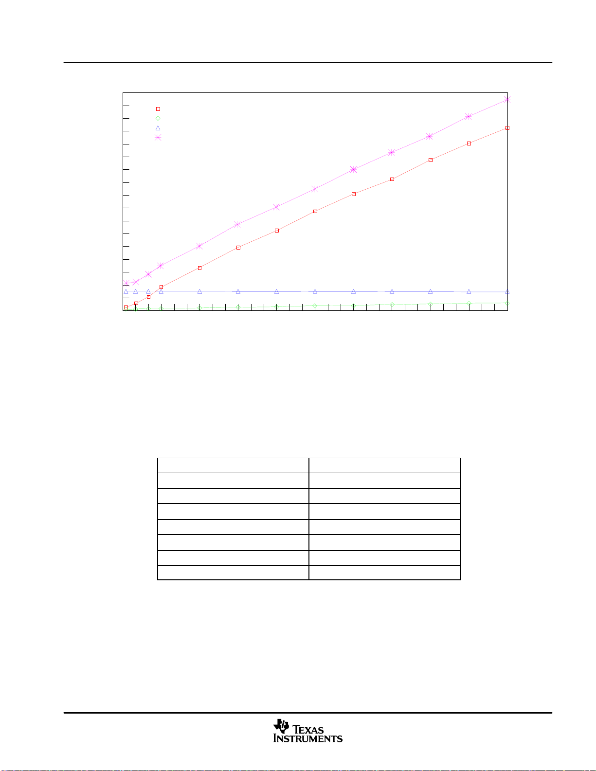
6.5 Current Consumption Graphs
ADVANCE INFORMATION
Electrical Specifications
240
210
180
150
120
Current (mA)
90
60
30
0
0 5 15 30 45 60 75 90 105 120 135 150
IDD
IDDIO
IDDA
Total
Figure 6−1. R2812/R2811 Typical Current Consumption (With Peripheral Clocks Enabled)
6.6 Reducing Current Consumption
SYSCLOCKOUT (MHz)
28x DSPs incorporate a unique method to reduce the device current consumption. A reduction in current
consumption can be achieved by turning off the clock to any peripheral module which is not used in a given
application. Table 6−1 indicates the typical reduction in current consumption achieved by turning off the clocks
to various peripherals.
Table 6−1. Typical Current Consumption by Various Peripherals (at 150 MHz)
PERIPHERAL MODULE
eCAN
EVA 6
EVB
ADC 8
SCI
SPI 5
McBSP 13
†
All peripheral clocks are disabled upon reset. Writing to/reading from peripheral registers is possible only after the peripheral clocks
are turned on.
‡
This number represents the current drawn by the digital portion of the ADC module. Turning off the clock to the ADC module results in the
elimination of the current drawn by the analog portion of the ADC (I
IDD CURRENT REDUCTION (mA)
12
6
‡
4
) as well.
CCA
†
6.7 Power Sequencing Requirements
Power sequencing is not required on the R281x devices. In other words, 3.3-V and 1.8-V (or 1.9-V) can ramp
together. R281x can also be used on boards that have F281x power sequencing implemented; however, if
the 1.8-V (or 1.9-V) rail lags the 3.3-V rail, the GPIO pins are undefined until the 1.8-V rail reaches at least
1 V.
June 2004 SPRS257
87
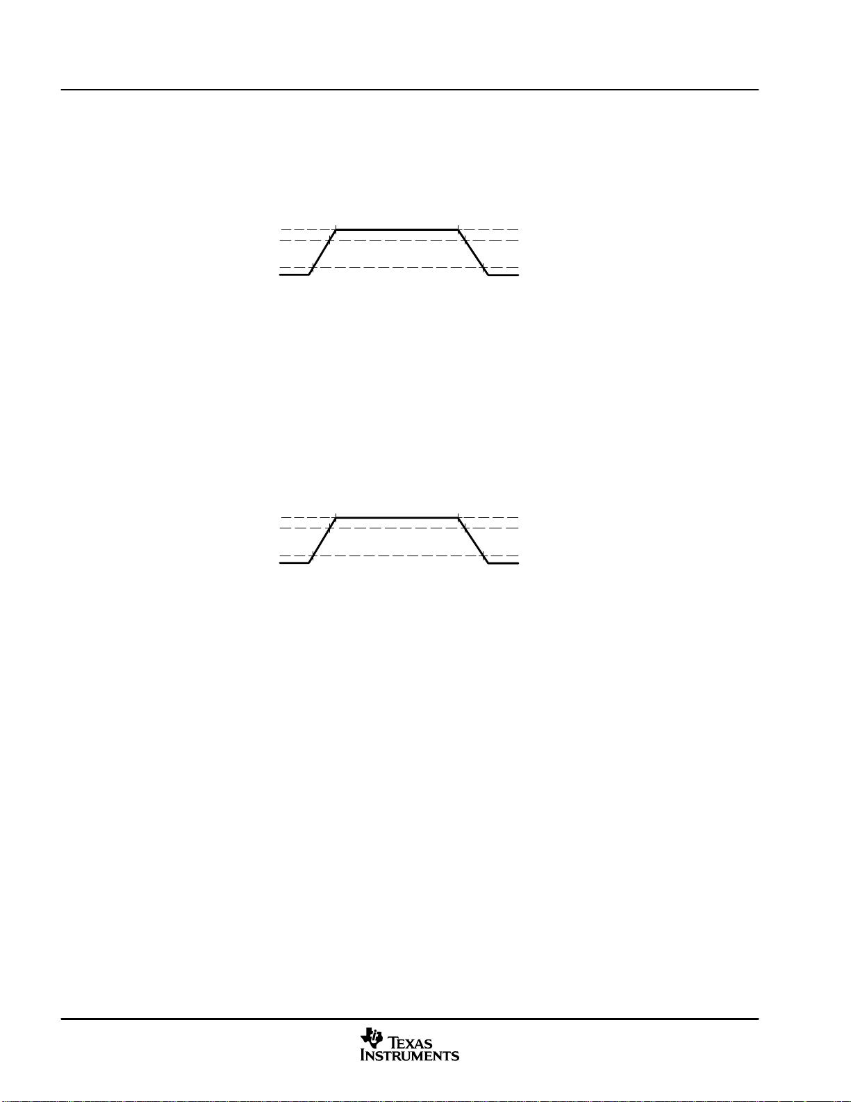
Electrical Specifications
ADVANCE INFORMATION
6.8 Signal Transition Levels
Note that some of the signals use different reference voltages, see the recommended operating conditions
table. Output levels are driven to a minimum logic-high level of 2.4 V and to a maximum logic-low level of
0.4 V.
Figure 6−2 shows output levels.
Output transition times are specified as follows:
• For a high-to-low transition, the level at which the output is said to be no longer high is below 80% of the
total voltage range and lower and the level at which the output is said to be low is 20% of the total voltage
range and lower.
• For a low-to-high transition, the level at which the output is said to be no longer low is 20% of the total
voltage range and higher and the level at which the output is said to be high is 80% of the total voltage
range and higher.
Figure 6−2. Output Levels
2.4 V (VOH)
80%
20%
0.4 V (VOL)
Figure 6−3 shows the input levels.
2.0 V (VIH)
90%
10%
0.8 V (VIL)
Figure 6−3. Input Levels
Input transition times are specified as follows:
• For a high-to-low transition on an input signal, the level at which the input is said to be no longer high is
90% of the total voltage range and lower and the level at which the input is said to be low is 10% of the
total voltage range and lower.
• For a low-to-high transition on an input signal, the level at which the input is said to be no longer low is
10% of the total voltage range and higher and the level at which the input is said to be high is 90% of the
total voltage range and higher.
NOTE: See the individual timing diagrams for levels used for testing timing parameters.
88
June 2004SPRS257
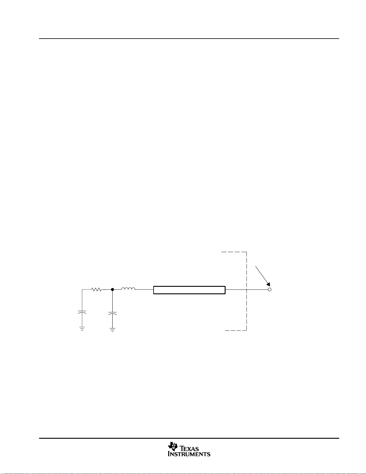
6.9 Timing Parameter Symbology
ADVANCE INFORMATION
Timing parameter symbols used are created in accordance with JEDEC Standard 100. To shorten the
symbols, some of the pin names and other related terminology have been abbreviated as follows:
Lowercase subscripts and their meanings: Letters and symbols and their meanings:
a access time H High
c cycle time (period) L Low
d delay time V Valid
f fall time X Unknown, changing, or don’t care level
h hold time Z High impedance
r rise time
su setup time
t transition time
v valid time
w pulse duration (width)
6.10 General Notes on Timing Parameters
All output signals from the 28x devices (including XCLKOUT) are derived from an internal clock such that all
output transitions for a given half-cycle occur with a minimum of skewing relative to each other.
Electrical Specifications
The signal combinations shown in the following timing diagrams may not necessarily represent actual cycles.
For actual cycle examples, see the appropriate cycle description section of this document.
6.11 Test Load Circuit
This test load circuit is used to measure all switching characteristics provided in this document.
Tester Pin Electronics
42 Ω 3.5 nH
4.0 pF 1.85 pF
NOTE: The data sheet provides timing at the device pin. For output timing analysis, the tester pin electronics and its transmission line effects
must be taken into account. A transmission line with a delay of 2 ns or longer can be used to produce the desired transmission line effect.
The transmission line is intended as a load only. It is not necessary to add or subtract the transmission line delay (2 ns or longer) from
the data sheet timing.
Input requirements in this data sheet are tested with an input slew rate of < 4 Volts per nanosecond (4 V/ns) at the device pin.
Transmission Line
Z0 = 50 Ω
(see note)
Figure 6−4. 3.3-V Test Load Circuit
Data Sheet Timing Reference Point
Output
Under
Test
Device Pin
(see note)
June 2004 SPRS257
89

Electrical Specifications
f
x
Input clock frequency
MHz
ADVANCE INFORMATION
6.12 Device Clock Table
This section provides the timing requirements and switching characteristics for the various clock options
available on R281x DSPs. Table 6−2 lists the cycle times of various clocks.
Table 6−2. TMS320R281x Clock Table and Nomenclature
MIN NOM MAX UNIT
t
, Cycle time 28.6 50 ns
On-chip oscillator clock
XCLKIN
SYSCLKOUT
XCLKOUT
HSPCLK
LSPCLK
ADC clock
SPI clock
McBSP
XTIMCLK
†
The maximum value for ADCCLK frequency is 25 MHz. For SYSCLKOUT values of 25 MHz or lower, ADCCLK has to be SYSCLKOUT/2 or lower.
ADCCLK = SYSCLKOUT is not a valid mode for any value of SYSCLKOUT.
‡
This is the default reset value if SYSCLKOUT = 150 MHz.
c(OSC)
Frequency 20 35 MHz
t
, Cycle time 6.67 250 ns
c(CI)
Frequency 4 150 MHz
t
, Cycle time 6.67 500 ns
c(SCO)
Frequency 2 150 MHz
t
, Cycle time 6.67 2000 ns
c(XCO)
Frequency 0.5 150 MHz
t
, Cycle time 6.67 13.3
c(HCO)
Frequency 75
t
, Cycle time 13.3 26.6
c(LCO)
Frequency 37.5
t
c(ADCCLK)
Frequency 25 MHz
t
c(SPC)
Frequency 20 MHz
t
c(CKG)
Frequency 20 MHz
t
c(XTIM)
Frequency 150 MHz
, Cycle time
, Cycle time 50 ns
, Cycle time 50 ns
, Cycle time 6.67 ns
†
40 ns
‡
‡
‡
‡
ns
150 MHz
ns
75 MHz
6.13 Clock Requirements and Characteristics
6.13.1 Input Clock Requirements
f
x
f
l
90
The clock provided at the XCLKIN pin generates the internal CPU clock cycle.
Table 6−3. Input Clock Frequency
PARAMETER MIN TYP MAX UNIT
Resonator 20 35
Input clock frequency
Limp mode clock frequency
Crystal
XCLKIN 4 150
20 35
2 MHz
MHz
June 2004SPRS257

Electrical Specifications
ADVANCE INFORMATION
Table 6−4. XCLKIN Timing Requirements − PLL Bypassed or Enabled
NO. MIN MAX UNIT
C8 t
C9 t
C10 t
C11 t
C12 t
c(CI)
f(CI)
r(CI)
w(CIL)
w(CIH)
Cycle time, XCLKIN 6.67 250 ns
Fall time, XCLKIN
Rise time, XCLKIN
Pulse duration, X1/XCLKIN low as a percentage of t
Pulse duration, X1/XCLKIN high as a percentage of t
c(CI)
c(CI)
Up to 30 MHz 6
30 MHz to 150 MHz
Up to 30 MHz 6
30 MHz to 150 MHz
40 60 %
40 60 %
2
2
Table 6−5. XCLKIN Timing Requirements − PLL Disabled
NO. MIN MAX UNIT
C8 t
C9 t
C10 t
C11 t
C12 t
c(CI)
f(CI)
r(CI)
w(CIL)
w(CIH)
Cycle time, XCLKIN 6.67 250 ns
Fall time, XCLKIN
Rise time, XCLKIN
Pulse duration, X1/XCLKIN low as a percentage of t
Pulse duration, X1/XCLKIN high as a percentage of t
c(CI)
c(CI)
Up to 30 MHz 6
30 MHz to 150 MHz
Up to 30 MHz 6
30 MHz to 150 MHz 2
XCLKIN ≤ 120 MHz 40 60
120 < XCLKIN ≤ 150 MHz 45 55
XCLKIN ≤ 120 MHz 40 60
120 < XCLKIN ≤ 150 MHz 45 55
2
ns
ns
ns
ns
%
%
Table 6−6. Possible PLL Configuration Modes
PLL MODE REMARKS SYSCLKOUT
Invoked by tying XPLLDIS pin low upon reset. PLL block is completely
PLL Disabled
PLL Bypassed
PLL Enabled
disabled. Clock input to the CPU (CLKIN) is directly derived from the clock
signal present at the X1/XCLKIN pin.
Default PLL configuration upon power-up, if PLL is not disabled. The PLL
itself is bypassed. However, the /2 module in the PLL block divides the clock
input at the X1/XCLKIN pin by two before feeding it to the CPU.
Achieved by writing a non-zero value “n” into PLLCR register. The /2 module
in the PLL block now divides the output of the PLL by two before feeding it to
the CPU.
XCLKIN
XCLKIN/2
(XCLKIN * n) / 2
June 2004 SPRS257
91

Electrical Specifications
ADVANCE INFORMATION
6.13.2 Output Clock Characteristics
Table 6−7. XCLKOUT Switching Characteristics (PLL Bypassed or Enabled)
No.
C1 t
c(XCO)
C3 t
f(XCO)
C4 t
r(XCO)
C5 t
w(XCOL)
C6 t
w(XCOH)
C7 t
p
†
A load of 40 pF is assumed for these parameters.
‡
H = 0.5t
§
c(XCO)
The PLL must be used for maximum frequency operation.
Cycle time, XCLKOUT 6.67
Fall time, XCLKOUT 2 ns
Rise time, XCLKOUT 2 ns
Pulse duration, XCLKOUT low H−2 H+2 ns
Pulse duration, XCLKOUT high H−2 H+2 ns
PLL lock time 131 072t
PARAMETER MIN TYP MAX UNIT
†‡
§
c(CI)
ns
ns
NOTES: A. The relationship of XCLKIN to XCLKOUT depends on the divide factor chosen. The waveform relationship shown in Figure 6−5 is
6.14 Reset Timing
†
‡
C10
C8
XCLKIN
(see Note A)
C1
C3
C4
XCLKOUT
(see Note B)
intended to illustrate the timing parameters only and may differ based on configuration.
B. XCLKOUT configured to reflect SYSCLKOUT.
Figure 6−5. Clock Timing
Table 6−8. Reset (XRS) Timing Requirements
t
w(RSL1)
t
w(RSL2)
t
w(WDRS)
t
d(EX)
‡
t
OSCST
t
su(XPLLDIS)
t
h(XPLLDIS)
t
h(XMP/MC)
t
h(boot-mode)
If external oscillator/clock source are used, reset time has to be low at least for 1 ms after VDD reaches 1.5 V.
Dependent on crystal/resonator and board design.
Pulse duration, stable XCLKIN to XRS high
Pulse duration, XRS low
Warm reset 8t
WD-initiated reset
Pulse duration, reset pulse generated by watchdog 512t
Delay time, address/data valid after XRS high
Oscillator start-up time
Setup time for XPLLDIS pin
Hold time for XPLLDIS pin
Hold time for XMP/MC pin
Hold time for boot-mode pins
†
MIN NOM MAX UNIT
8t
c(CI)
c(CI)
1 10 ms
16t
c(CI)
16t
c(CI)
16t
c(CI)
c(CI)
§
2520t
C6
512t
32t
C5
c(CI)
c(CI)
c(CI)
C9
cycles
cycles
cycles
cycles
cycles
cycles
cycles
cycles
92
June 2004SPRS257

Electrical Specifications
ADVANCE INFORMATION
V
, V
DDIO
DDAIO
DDAn
(3.3 V)
V
(See Note A)
, V
V
DD
DD1
(1.8 V (or 1.9 V))
XCLKIN
XCLKOUT
XRS
Address/Data/
Control
XF/XPLLDIS
X1
†
,
2.5 V
0.3 V
XCLKIN/8 (See Note B)
User-Code Dependent
t
OSCST
t
w(RSL1)
Address/Data Valid. Internal Boot-ROM Code Execution Phase
User-Code Execution Phase
User-Code Dependent
t
h(XPLLDIS)
GPIOF14
XPLLDIS
(Don’t Care)
t
su(XPLLDIS)
Sampling
t
d(EX)
XMP/MC
Boot-Mode Pins
See Note D
I/O Pins
NOTES: A. V
B. Upon power up, SYSCLKOUT is XCLKIN/2 if the PLL is enabled. Since both the XTIMCLK and CLKMODE bits in the
C. After reset, the Boot ROM code executes instructions for 1260 SYSCLKOUT cycles (SYSCLKOUT = XCLKIN/2) and then
D. The state of the GPIO pins is undefined (i.e., they could be input or output) until the 1.8-V (or 1.9-V) supply reaches at least
t
h(XMP/MC)
t
h(boot-mode)
see Note C)
(
User-Code Dependent
(Don’t Care)
GPIO Pins as Input
Boot-ROM Execution Starts
Peripheral/GPIO Function
Based on Boot Code
GPIO Pins as Input (State Depends on Internal PU/PD)
User-Code Dependent
DDAn
− V
DDA1/VDDA2
and AV
DDREFBG
XINTCNF2 register come up with a reset state of 1, SYSCLKOUT is further divided by 4 before it appears at XCLKOUT. This
explains why XCLKOUT = XCLKIN/8 during this phase.
samples BOOT Mode pins. Based on the status of the Boot Mode pin, the boot code branches to destination memory or boot
code function in ROM. The BOOT Mode pins should be held high/low for at least 2520 XCLKIN cycles from boot ROM
execution time for proper selection of Boot modes.
If Boot ROM code executes after power-on conditions (in debugger environment), the Boot code execution time is based on
the current SYSCLKOUT speed. The SYSCLKOUT will be based on user environment and could be with or without PLL
enabled.
1 V and 3.3-V supply reaches 2.5 V.
Figure 6−6. Power-on Reset in Microcomputer Mode (XMP/MC = 0)
June 2004 SPRS257
93

Electrical Specifications
ADVANCE INFORMATION
V
, V
V
DDAIO
VDD, V
DD1
Address/Data/
DDIO
(1.8 V (or
XCLKIN
XCLKOUT
XF/XPLLDIS
DDAn
(3.3 V)
1.9 V))
X1
XRS
Control
XMP/MC
,
2.5 V
0.3 V
t
OSCST
(Don’t Care)
XPLLDIS
(Don’t Care)
XCLKIN/8 (See Note A)
t
w(RSL)
t
d(EX)
Sampling
t
su(XPLLDIS)
t
h(XMP/MC)
User-Code Dependent
Address/Data/Control Valid Execution
Begins From External Boot Address 0x3FFFC0
t
h(XPLLDIS)
GPIOF14/XF (User-Code Dependent)
(Don’t Care)
NOTES: A. Upon power up, SYSCLKOUT is XCLKIN/2 if the PLL is enabled. Since both the XTIMCLK and CLKMODE bits in the XINTCNF2
I/O Pins
See Note B
Input Configuration (State Depends on Internal PU/PD)
User-Code Dependent
register come up with a reset state of 1, SYSCLKOUT is further divided by 4 before it appears at XCLKOUT. This explains why
XCLKOUT = XCLKIN/8 during this phase.
B. The state of the GPIO pins is undefined (i.e., they could be input or output) until the 1.8-V (or 1.9-V) supply reaches at least 1 V
and 3.3-V supply reaches 2.5 V..
Figure 6−7. Power-on Reset in Microprocessor Mode (XMP/MC = 1)
94
June 2004SPRS257

XCLKIN
ADVANCE INFORMATION
X1
Electrical Specifications
XCLKOUT
(XCLKIN * 5)
t
XRS
Address/Data/
Control
XF/XPLLDIS
XMP/MC
Boot-Mode Pins
I/O Pins
†
After reset, the Boot ROM code executes instructions for 1260 SYSCLKOUT cycles (SYSCLKOUT = XCLKIN/2) and then samples BOOT
Mode pins. Based on the status of the Boot Mode pin, the boot code branches to destination memory or boot code function in ROM. The
BOOT Mode pins should be held high/low for at least 2520 XCLKIN cycles from boot ROM execution time for proper selection of Boot
modes.
If Boot ROM code executes after power-on conditions (in debugger environment), the Boot code execution time is based on the current
SYSCLKOUT speed. The SYSCLKOUT will be based on user environment and could be with or without PLL enabled.
User-Code Execution
GPIOF14/XF
(Don’t Care)
Boot-ROM Execution Starts
Peripheral/GPIO Function
User-Code Dependent
w(RSL2)
t
d(EX)
(Don’t Care)
t
su(XPLLDIS)
(Don’t Care)
XPLLDIS
Sampling
t
h(XMP/MC)
GPIO Pins as Input
GPIO Pins as Input (State Depends on Internal PU/PD)
XCLKIN/8
User-Code Dependent
User-Code Execution Phase
t
h(XPLLDIS)
GPIOF14
User-Code Dependent
(Don’t Care)
t
h(boot-mode)
Peripheral/GPIO Function
User-Code Execution Starts
User-Code Dependent
†
Figure 6−8. Warm Reset in Microcomputer Mode
June 2004 SPRS257
95

Electrical Specifications
ADVANCE INFORMATION
X1/XCLKIN
SYSCLKOUT
Write to PLLCR
XCLKIN*2
(Current CPU
Frequency)
Figure 6−9. Effect of Writing Into PLLCR Register
XCLKIN/2
(CPU Frequency While PLL is Stabilizing
With the Desired Frequency. This Period
(PLL Lock-up Time, t
131072 XCLKIN Cycles Long.)
) is
p
XCLKIN*4
(Changed CPU Frequency)
96
June 2004SPRS257
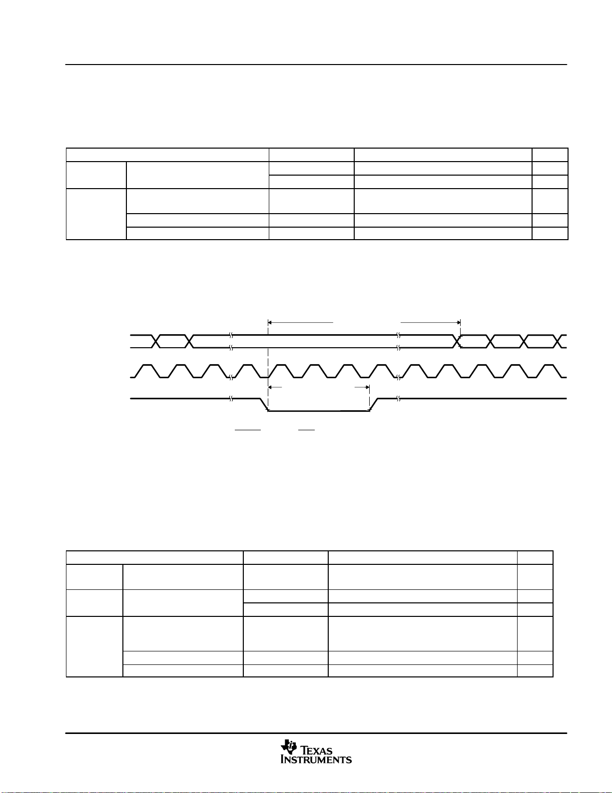
Electrical Specifications
p
Pulse duration, external wake-up
Pulse duration, external
t
ADVANCE INFORMATION
6.15 Low-Power Mode Wakeup Timing
Table 6−9 is also the IDLE Mode Wake-Up Timing Requirements table.
Table 6−9. IDLE Mode Switching Characteristics
PARAMETER TEST CONDITIONS MIN TYP MAX UNIT
t
w(WAKE-INT)
t
d(WAKE-IDLE)
Pulse duration, external wake-u
signal
Delay time, external wake signal to
program execution resume
‡
− Wake-up from SARAM Without input qualifier 8 * t
Without input qualifier 2*t
With input qualifier 1*t
− Wake-up from SARAM With input qualifier 8 * t
†
Input Qualification Time (IQT) = [5 x QUALPRD x 2] * t
‡
This is the time taken to begin execution of the instruction that immediately follows the IDLE instruction. Execution of an ISR (triggered by the
c(SCO)
c(SCO)
c(SCO)
c(SCO)
+ IQT
c(SCO)
+ IQT
†
†
wake-up) signal involves additional latency.
t
d(WAKE−IDLE)
A0−A15
Cycles
Cycles
Cycles
Cycles
XCLKOUT
WAKE INT
†
XCLKOUT = SYSCLKOUT
‡
WAKE INT can be any enabled interrupt, WDINT, XNMI, or XRS.
†
t
w(WAKE−INT)
‡
Figure 6−10. IDLE Entry and Exit Timing
Table 6−10 is also the STANDBY Mode Wake-Up Timing Requirements table.
Table 6−10. STANDBY Mode Switching Characteristics
PARAMETER TEST CONDITIONS MIN TYP MAX UNIT
t
d(IDLE-XCOH)
t
w(WAKE-INT)
d(WAKE-STBY)
†
QUALSTDBY is a 6-bit field in the LPMCR0 register.
‡
This is the time taken to begin execution of the instruction that immediately follows the IDLE instruction. Execution of an ISR (triggered by the
wake-up) signal involves additional latency.
Delay time, IDLE instruction
executed to XCLKOUT high
Pulse duration, external
wake-up signal
Without input qualifier 12 * t
With input qualifier (2 + QUALSTDBY)† * t
32 * t
Delay time, external wake
signal to program execution
‡
resume
− Wake-up from SARAM Without input qualifier 12 * t
− Wake-up from SARAM With input qualifier 12 * t
c(CI)
+ t
w(WAKE-INT)
c(SCO)
c(CI)
c(CI)
c(CI)
12 * t
c(CI)
Cycles
Cycles
Cycles
Cycles
Cycles
June 2004 SPRS257
97
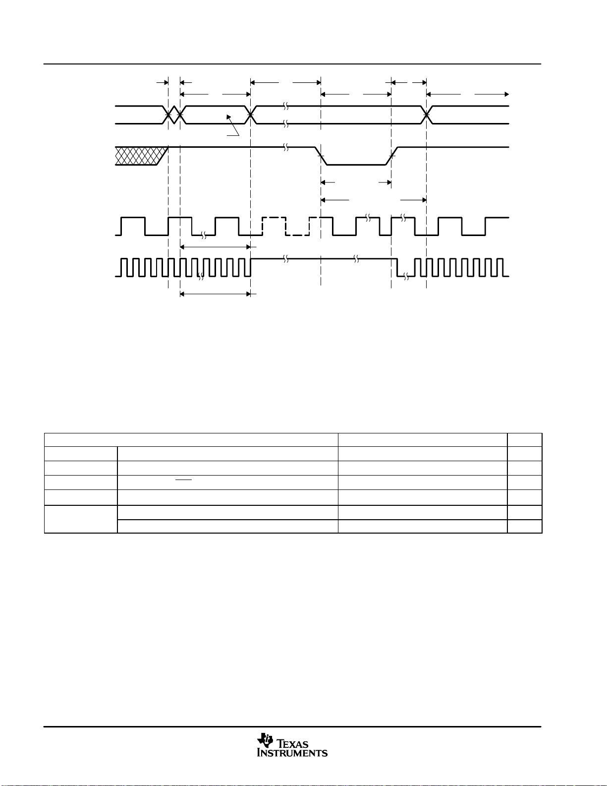
Electrical Specifications
ADVANCE INFORMATION
A
C
B
Device
Status
STANDBY Normal ExecutionSTANDBY
Flushing Pipeline
Wake−up
Signal
t
X1/XCLKIN
t
d(IDLE−XCOH)
XCLKOUT
†
32 SYSCLKOUT Cycles
NOTES: A. IDLE instruction is executed to put the device into STANDBY mode.
B. The PLL block responds to the STANDBY signal. SYSCLKOUT is held for approximately 32 cycles before being turned
off. This 32−cycle delay enables the CPU pipe and any other pending operations to flush properly.
C. The device is now in STANDBY mode.
D. The external wake−up signal is driven active (negative edge triggered shown as an example).
E. After a latency period, the STANDBY mode is exited.
F. Normal operation resumes. The device will respond to the interrupt (if enabled).
D
w(WAKE-INT)
t
d(WAKE-STBY)
E
F
t
d(IDLE-XCOH)
t
w(WAKE-XNMI)
t
w(WAKE-XRS)
t
p
t
d(wake)
Figure 6−11. STANDBY Entry and Exit Timing
Table 6−11. HALT Mode Switching Characteristics
PARAMETER MIN TYP MAX UNIT
Delay time, IDLE instruction executed to XCLKOUT high
Pulse duration, XNMI wakeup signal
Pulse duration, XRS wakeup signal
PLL lock-up time
Delay time, PLL lock to program execution resume
− Wake-up from SARAM
32 * t
c(SCO)
2 * t
8 * t
c(CI)
c(CI)
45 * t
c(SCO)
131072 * t
c(CI)
Cycles
Cycles
Cycles
Cycles
35*tc(SCO) Cycles
98
June 2004SPRS257
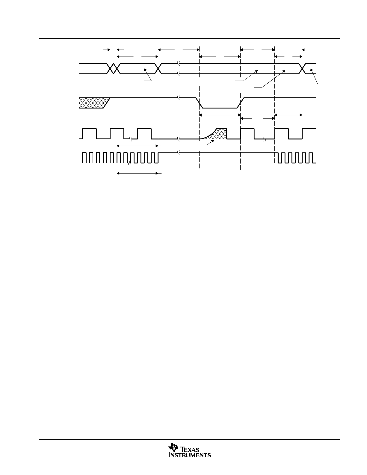
Electrical Specifications
ADVANCE INFORMATION
A
B
Device
Status
Flushing Pipeline
XNMI
X1/XCLKIN
XCLKOUT
†
XCLKOUT = SYSCLKOUT
NOTES: A. IDLE instruction is executed to put the device into HALT mode.
†
B. The PLL block responds to the HALT signal. SYSCLKOUT is held for another 32 cycles before the oscillator is turned off and the
CLKIN to the core is stopped. This 32-cycle delay enables the CPU pipe and any other pending operations to flush properly.
C. Clocks to the device are turned off and the internal oscillator and PLL are shut down. The device is now in HALT mode and
consumes absolute minimum power.
D. When XNMI is driven active (negative edge triggered shown , as an example), the oscillator is turned on; but the PLL is not
activated.
E. When XNMI is deactivated, it initiates the PLL lock sequence, which takes 131,072 X1/XCLKIN cycles.
F. When CLKIN to the core is enabled, the device will respond to the interrupt (if enabled), after a latency. The HALT mode is now
exited.
G. Normal operation resumes.
C
HALT HALT
PLL Lock−up Time
t
w(WAKE−XNMI)
t
d(IDLE−XCOH)
32 SYSCLKOUT Cycles
E
D
Wake−up Latency
t
p
Oscillator Start-up Time
F
Normal
Execution
t
d(INT)
G
Figure 6−12. HALT Wakeup Using XNMI
June 2004 SPRS257
99

Electrical Specifications
ADVANCE INFORMATION
6.16 Event Manager Interface
6.16.1 PWM Timing
PWM refers to all PWM outputs on EVA and EVB.
Table 6−12. PWM Switching Characteristics
PARAMETER
§
t
w(PWM)
t
d(PWM)XCO
†
See the GPIO output timing for fall/rise times for PWM pins.
‡
PWM pin toggling frequency is limited by the GPIO output buffer switching frequency (20 MHz).
§
PWM outputs may be 100%, 0%, or increments of t
Pulse duration, PWMx output high/low
Delay time, XCLKOUT high to PWMx output switching
with respect to the PWM period.
c(HCO)
TEST CONDITIONS MIN MAX UNIT
XCLKOUT = SYSCLKOUT/4 10 ns
Table 6−13. Timer and Capture Unit Timing Requirements
t
w(TDIR)
t
w(CAP)
t
w(TCLKINL)
t
w(TCLKINH)
t
c(TCLKIN)
¶
The QUALPRD bit field value can range from 0 (no qualification) through 0xFF (510 SYSCLKOUT cycles). The qualification sampling period is
Pulse duration, TDIRx low/high
Pulse duration, CAPx input low/high
Pulse duration, TCLKINx low as a percentage of TCLKINx cycle time
Pulse duration, TCLKINx high as a percentage of TCLKINx cycle time
Cycle time, TCLKINx
2n SYSCLKOUT cycles, where “n” is the value stored in the QUALPRD bit field. As an example, when QUALPRD = 1, the qualification sampling
period is 1 x 2 = 2 SYSCLKOUT cycles (i.e., the input is sampled every 2 SYSCLKOUT cycles). Six such samples will be taken over five sampling
windows, each window being 2n SYSCLKOUT cycles. For QUALPRD = 1, the minimum width that is needed is 5 x 2 = 10 SYSCLKOUT cycles.
However, since the external signal is driven asynchronously, a 11-SYSCLKOUT-wide pulse ensures reliable recognition.
#
Maximum input frequency to the QEP = min[HSPCLK/2, 20 MHz]
||
Input Qualification Time (IQT) = [5 x QUALPRD x 2] * t
c(SCO)
Without input qualifier 2 * t
With input qualifier
Without input qualifier 2 * t
With input qualifier
†‡
25 ns
¶#
MIN MAX UNIT
1 * t
1 * t
c(SCO)
c(SCO)
c(SCO)
c(SCO)
+ IQT
+ IQT
||
||
40 60 %
40 60 %
4 * t
c(HCO)
cycles
cycles
ns
XCLKOUT
†
PWMx
†
XCLKOUT = SYSCLKOUT
XCLKOUT
†
TDIRx
†
XCLKOUT = SYSCLKOUT
t
d(PWM)XCO
t
w(PWM)
Figure 6−13. PWM Output Timing
t
w(TDIR)
Figure 6−14. TDIRx Timing
100
June 2004SPRS257
 Loading...