

Texas Instruments TMS320LC57SRBK80, TMS320LC57SRBK50, TMS320LC57SRBK, TMS320LC57SPJEA80, TMS320LC57SPJEA50 Datasheet
...
TMS320C5x, TMS320LC5x
DIGITAL SIGNAL PROCESSORS
SPRS030A – APRIL 1995 – REVISED APRIL 1996
1
POST OFFICE BOX 1443 • HOUSTON, TEXAS 77251–1443
D
Powerful 16-Bit TMS320C5x CPU
D
20-, 25-, 35-, and 50-ns Single-Cycle
Instruction Execution Time for 5-V
Operation
D
25-, 40-, and 50-ns Single-Cycle Instruction
Execution Time for 3-V Operation
D
Single-Cycle 16 × 16-Bit Multiply/Add
D
224K × 16-Bit Maximum Addressable
External Memory Space (64K Program, 64K
Data, 64K I/O, and 32K Global)
D
2K, 4K, 8K, 16K, 32K × 16-Bit Single-Access
On-Chip Program ROM
D
1K, 3K, 6K, 9K × 16-Bit Single-Access
On-Chip Program/Data RAM (SARAM)
D
1K Dual-Access On-Chip Program/Data
RAM (DARAM)
D
Full-Duplex Synchronous Serial Port for
Coder/Decoder Interface
D
Time-Division-Multiplexed (TDM) Serial Port
D
Hardware or Software Wait-State
Generation Capability
D
On-Chip Timer for Control Operations
D
Repeat Instructions for Efficient Use of
Program Space
D
Buffered Serial Port
D
Host Port Interface
D
Multiple Phase-Locked Loop (PLL)
Clocking Options (×1, ×2, ×3, ×4, ×5, ×9
Depending on Device)
D
Block Moves for Data/Program
Management
D
On-Chip Scan-Based Emulation Logic
D
Boundary Scan
D
Five Packaging Options
– 100-Pin Quad Flat Package (PJ Suffix)
– 100-Pin Thin Quad Flat Package
(PZ Suffix)
– 128-Pin Thin Quad Flat Package
(PBK Suffix)
– 132-Pin Quad Flat Package (PQ Suffix)
– 144-Pin Thin Quad Flat Package
(PGE Suffix)
D
Low Power Dissipation and Power-Down
Modes:
– 47 mA (2.35 mA/MIP) at 5 V, 40-MHz
Clock (Average)
– 23 mA (1.15 mA/MIP) at 3 V, 40-MHz
Clock (Average)
– 10 mA at 5 V, 40-MHz Clock (IDLE1 Mode)
– 3 mA at 5 V, 40-MHz Clock (IDLE2 Mode)
– 5 µA at 5 V, Clocks Off (IDLE2 Mode)
D
High-Performance Static CMOS T echnology
D
IEEE Standard 1149.1† Test-Access Port
(JTAG)
description
The TMS320C5x generation of the Texas Instruments (TI) TMS320 digital signal processors (DSPs) is
fabricated with static CMOS integrated circuit technology; the architectural design is based upon that of an
earlier TI DSP, the TMS320C25. The combination of advanced Harvard architecture, on-chip peripherals,
on-chip memory , and a highly specialized instruction set is the basis of the operational flexibility and speed of
the ’C5x
‡
devices. They execute up to 50 million instructions per second (MIPS).
The ’C5x devices offer these advantages:
D
Enhanced TMS320 architectural design for increased performance and versatility
D
Modular architectural design for fast development of spin-off devices
D
Advanced integrated-circuit processing technology for increased performance
D
Upward-compatible source code (source code for ’C1x and ’C2x DSPs is upward compatible with ’C5x DSPs.)
D
Enhanced TMS320 instruction set for faster algorithms and for optimized high-level language operation
D
New static-design techniques for minimizing power consumption and maximizing radiation tolerance
Please be aware that an important notice concerning availability, standard warranty, and use in critical applications of
Texas Instruments semiconductor products and disclaimers thereto appears at the end of this data sheet.
PRODUCTION DATA information is current as of publication date.
Products conform to specifications per the terms of Texas Instruments
standard warranty. Production processing does not necessarily include
testing of all parameters.
Copyright 1996, Texas Instruments Incorporated
TI is a trademark of Texas Instruments Incorporated.
†
IEEE Standard 1149.1–1990, IEEE Standard Test-Access Port and Boundary-Scan Architecture
‡
References to ’C5x in this document include both TMS320C5x and TMS320LC5x devices unless specified otherwise.
TMS320C5x, TMS320LC5x
DIGITAL SIGNAL PROCESSORS
SPRS030A – APRIL 1995 – REVISED APRIL 1996
2
POST OFFICE BOX 1443 • HOUSTON, TEXAS 77251–1443
description (continued)
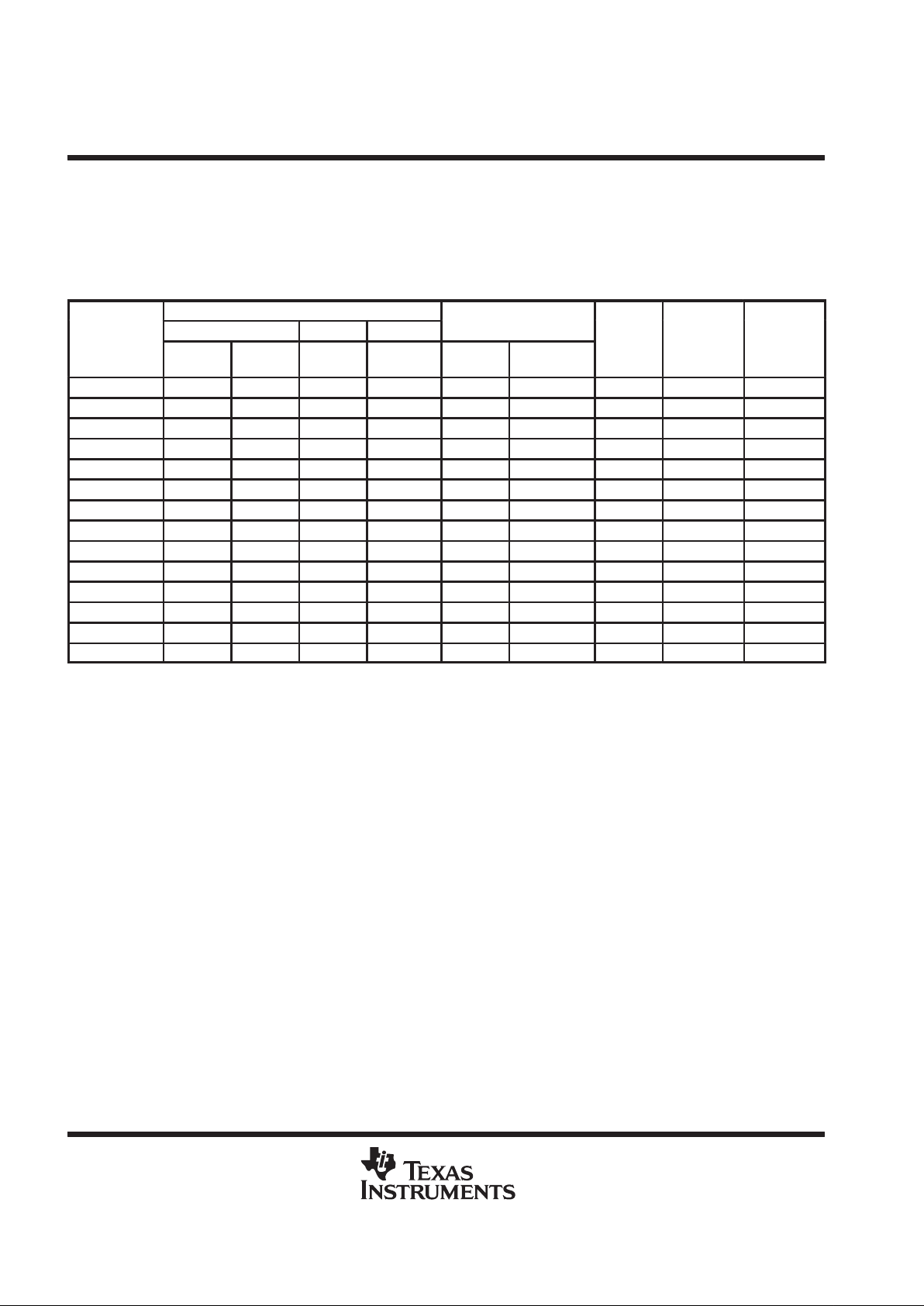
T able 1 provides a comparison of the devices in the ’C5x generation. It shows the capacity of on-chip RAM and
ROM memories, number of serial and parallel I/O ports, execution time of one machine cycle, and type of
package with total pin count.
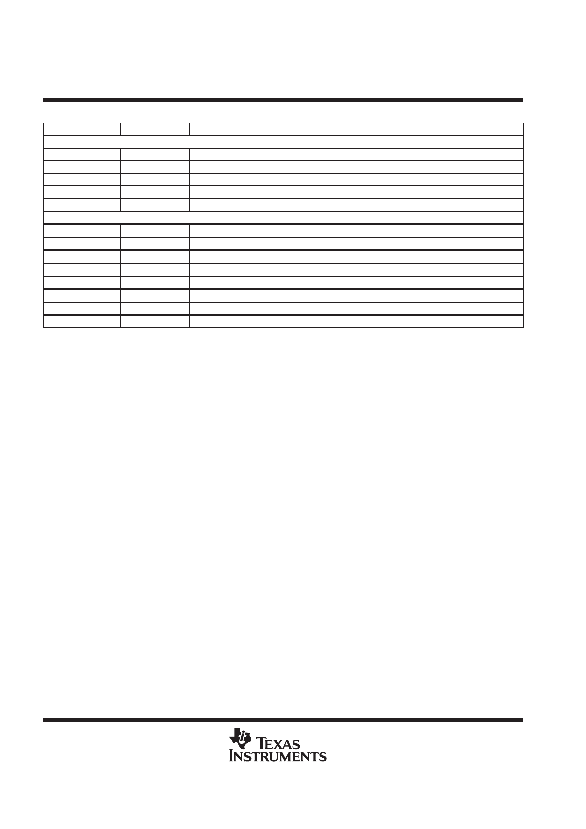
Table 1. Characteristics of the ’C5x Processors
ON-CHIP MEMORY (16-BIT WORDS)
TMS320
DARAM SARAM ROM
I/O PORTS
POWER
CYCLE
PACKAGE
DEVICES
DATA
DATA +
PROG
DATA +
PROG
PROG SERIAL PARALLEL
†
SUPPLY
(V)
TIME
(ns)
TYPE
QFP
‡
TMS320C50 544 512 9K 2K
§
2 64K 5 50/35/25 132 pin
TMS320LC50 544 512 9K 2K
§
2 64K 3.3 50/40/25 132 pin
TMS320C51 544 512 1K 8K
§
2 64K 5 50/35/25/20 100/132 pin
TMS320LC51 544 512 1K 8K
§
2 64K 3.3 50/40/25 100/132 pin
TMS320C52 544 512 – 4K
§
1
¶
64K 5 50/35/25/20 100 pin
TMS320LC52 544 512 – 4K
§
1
¶
64K 3.3 50/40/25 100 pin
TMS320C53 544 512 3K 16K
§
2 64K 5 50/35/25 132 pin
TMS320LC53 544 512 3K 16K
§
2 64K 3.3 50/40/25 132 pin
TMS320C53S 544 512 3K 16K
§
2
¶
64K 5 50/35/25 100 pin
TMS320LC53S 544 512 3K 16K
§
2
¶
64K 3.3 50/40/25 100 pin
TMS320LC56 544 512 6K 32K 2
#
64K 3.3 35/25 100 pin
TMS320LC57 544 512 6K 32K 2
#
64K + HPI
||
3.3 35/25 128 pin
TMS320C57S 544 512 6K 2K
§
2
#
64K + HPI
||
5 50/35/25 144 pin
TMS320LC57S 544 512 6K 2K
§
2
#
64K + HPI
||
3.3 50/35 144 pin
†
Sixteen of the 64K parallel I/O ports are memory mapped.
‡
QFP = Quad flatpack
§
ROM boot loader available
¶
TDM serial port not available
#
Includes auto-buffered serial port (BSP) but TDM serial port not available
||
HPI = Host port interface
Pinouts for each package are device-specific.
TMS320C5x, TMS320LC5x
DIGITAL SIGNAL PROCESSORS
SPRS030A – APRIL 1995 – REVISED APRIL 1996
3
POST OFFICE BOX 1443 • HOUSTON, TEXAS 77251–1443
TMS320C50, TMS320LC50, TMS320C51, TMS320LC51, TMS320C53, TMS320LC53
PQ PACKAGE
(TOP VIEW)
WE
DDAVDDA
V
V
SSD
V
SSD
D7
D6
D5
D4
D3
D2
D1
D0
TMS
V
DDD
V
DDD
TCK
V
SSD
V
SSD
INT1
INT2
INT3
INT4
NMI
DR
TDR
FSR
CLKR
V
DDA
V
DDA
V
SSC
V
SSC
DS
IS
PS
R/W
STRB
BR
CLKIN2
X2/CLKIN
X1
V
DDC
V
DDC
TDO
V
SSI
V
SSI
FSX
TFSX/TFRM
DX
TDX
HOLDA
XF
CLKOUT1
NC
IACK
V
DDI
V
DDI
17 16 15 14 13 12 11 10 9 8 7 6 5 4 3 2 1 132 131 130 129 128 127 126 125 124 123 122 121 120 119 118 117
116
115
114
113
112
111
110
109
108
107
106
105
104
103
102
101
100
99
98
97
96
95
94
93
92
91
90
89
88
87
86
85
84
36
50
49
48
47
46
45
44
43
42
41
40
39
38
37
35
34
33
32
31
30
29
28
27
26
25
24
23
22
21
20
19
18
DDDVDDD
VD8D9
D10
D11
D12
D13
D14
D15
MP/MC
TRST
IAQ
SSIVSSI
V
51 52 53 54 55 56 57 58 59 60 61 62 63 64 65 66 67 68 69 70 71 72 73 74 75 76 77 78 80 81 82 83
DDCVDDC
V
BIO
HOLD
READYRSTCLKR
TFSR/TADD
CLKX
TCLKX
TOUT
EMU1/OFF
EMU0
SSCVSSC
V
SSAVSSA
V
A0A1A2A3A4A5A6A7A8
TDI
A9
CLKMD1
A10
A11
A12
A13
A14
A15
DDIVDDI
V
SSAVSSA
V
RD
79
NC
NC
NC
NC
NC
NC
NC
NC
NC
NC
NC
NC
NC
NC
NC
NC
CLKMD2
NC
NC
NC
NOTE: NC = No connect (These pins are reserved.)
TMS320C5x, TMS320LC5x
DIGITAL SIGNAL PROCESSORS
SPRS030A – APRIL 1995 – REVISED APRIL 1996
4
POST OFFICE BOX 1443 • HOUSTON, TEXAS 77251–1443
Pin Functions for Devices in the PQ Package
SIGNAL TYPE DESCRIPTION
PARALLEL INTERFACE BUS
A0–A15 I/O/Z 16-bit external address bus (MSB: A15, LSB: A0)
D0–D15 I/O/Z 16-bit external data bus (MSB: D15, LSB: D0)
PS, DS, IS O/Z Program, data, and I/O space select outputs, respectively
STRB I/O/Z Timing strobe for external cycles and external DMA
R/W I/O/Z Read/write select for external cycles and external DMA
RD, WE O/Z Read and write strobes, respectively, for external cycles
READY I External bus ready/wait-state control input
BR I/O/Z Bus request. Arbitrates global memory and external DMA
SYSTEM INTERFACE/CONTROL SIGNALS
RS I Reset. Initializes device and sets PC to zero
MP/MC I Microprocessor/microcomputer mode select. Enables internal ROM
HOLD I Puts parallel I/F bus in high-impedance state after current cycle
HOLDA O/Z Hold acknowledge. Indicates external bus in hold state
XF O/Z External flag output. Set/cleared through software
BIO I I/O branch input. Implements conditional branches
TOUT O/Z Timer output signal. Indicates output of internal timer
IAQ O/Z Instruction acquisition signal
IACK O/Z Interrupt acknowledge signal
INT1–INT4 I External interrupt inputs
NMI I Nonmaskable external interrupt
SERIAL PORT INTERFACE (SPI)
DR I Serial receive-data input
DX O/Z Serial transmit-data output. In high-impedance state when not transmitting
CLKR I Serial receive-data clock input
CLKX I/O/Z Serial transmit-data clock. Internal or external source
FSR I Serial receive-frame-synchronization input
FSX I/O/Z Serial transmit-frame-synchronization signal. Internal or external source
TDM SERIAL-PORT INTERFACE
TDR I TDM serial receive-data input
TDX O/Z TDM serial transmit-data output. In high-impedance state when not transmitting
TCLKR I TDM serial receive-data clock input
TCLKX I/O/Z TDM serial transmit-data clock. Internal or external source
TFSR / TADD I/O/Z
TDM serial receive-frame-synchronization input. In the TDM mode, TFSR/TADD is used to output/
input the address of the port.
TFSX /TFRM I
TDM serial transmit-frame-synchronization signal. Internal or external source. In the TDM mode,
TFSX/TFRM becomes TFRM, the TDM frame synchronization.
LEGEND:
I = Input
O = Output
Z = High impedance
TMS320C5x, TMS320LC5x
DIGITAL SIGNAL PROCESSORS
SPRS030A – APRIL 1995 – REVISED APRIL 1996
5
POST OFFICE BOX 1443 • HOUSTON, TEXAS 77251–1443
Pin Functions for Devices in the PQ Package (Continued)
EMULATION/IEEE STANDARD 1149.1 TEST ACCESS PORT (TAP)
TDI I TAP scan data input
TDO O/Z TAP scan data output
TMS I TAP mode select input
TCK I TAP clock input
TRST I TAP reset (with pulldown resistor). Disables TAP when low
EMU0 I/O/Z Emulation control 0. Reserved for emulation use
EMU1/OFF I/O/Z Emulation control 1. Puts outputs in high-impedance state when low
CLOCK GENERATION AND CONTROL
X1 O Oscillator output
X2/CLKIN I Clock/oscillator input
CLKIN2 I Clock input
CLKMD1, CLKMD2 I Clock-mode select inputs
CLKOUT1 O/Z Device system-clock output
POWER SUPPLY CONNECTIONS
V
DDA
S Supply connection, address-bus output
V
DDD
S Supply connection, data-bus output
V
DDC
S Supply connection, control output
V
DDI
S Supply connection, internal logic
V
SSA
S Supply connection, address-bus output
V
SSD
S Supply connection, data-bus output
V
SSC
S Supply connection, control output
V
SSI
S Supply connection, internal logic
LEGEND:
I = Input
O = Output
S = Supply
Z = High impedance
TMS320C5x, TMS320LC5x
DIGITAL SIGNAL PROCESSORS
SPRS030A – APRIL 1995 – REVISED APRIL 1996
6
POST OFFICE BOX 1443 • HOUSTON, TEXAS 77251–1443
HINT
EMU0
EMU1/OFF
V
SSC
V
SSC
TOUT
BCLKX
CLKX
BFSR
BCLKR
RS
READY
HOLD
BIO
V
DDC
V
DDC
IAQ
TRST
V
SSI
V
SSI
MP/MC
D15
D14
D13
D12
D11
D10
D9
D8
V
DDD
V
DDD
HD1
WE
RD
HD0
HRDY
V
DDA
A15
A14
A13
A12
A11
A10
CLKMD1
V
SSA
V
SSA
TDI
HDS1
HDS2
V
DDI
A9
A8
A7
A6
A5
A4
A3
A2
A1
A0
V
SSA
HCS
96
95
94
93
92
91
90
89
88
87
86
85
84
83
82
81
80
79
78
77
76
75
74
73
72
71
70
69
68
67
66
65
1
2
3
4
5
6
7
8
9
10
11
12
13
14
15
16
17
18
19
20
21
22
23
24
25
26
27
28
29
30
31
32
128
33
127 126 125 124 123 122 121 120 119 118 117 116 115 114 113 112 111 110 109 108 107 106 105 104 103 102 101 100 99 98 97
34 35 36 37 38 39 40 41 42 43 44 45 46 47 48 49 50 51 52 53 54 55 56 57 58 59 60 61 62 63 64
SSDVSSD
V
D7 V
D6
CLKOUT1
D5XFD4
HOLDAD3BDXD2DXD1HD7D0BFSX
TMS
HD6
DDD
DDD
TCK
CLKMD2
SSD
SSD
INT1
INT2
TDO
INT3
INT4
X1
NMI
X2/CLKIN
CLKMD3
STRB
R/ W
DR
BDR
HD3
FSR
IS
CLKR
PS
DDA
HD2
DDA
HAS
DDC
DDI
DDI
V
V
V
V
V
V
V
V
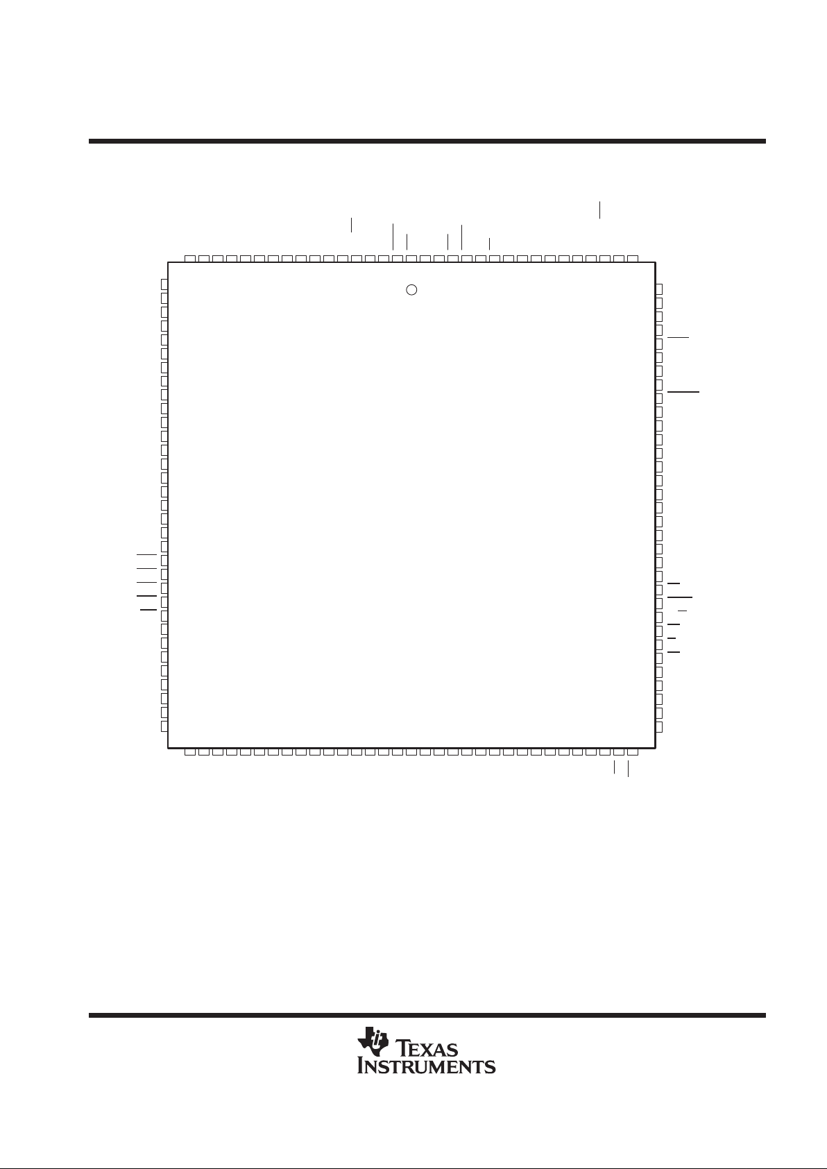
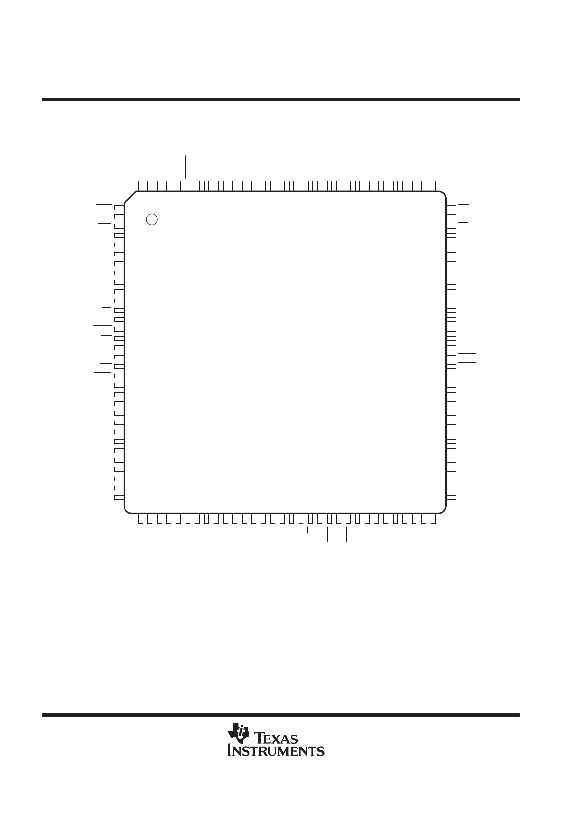
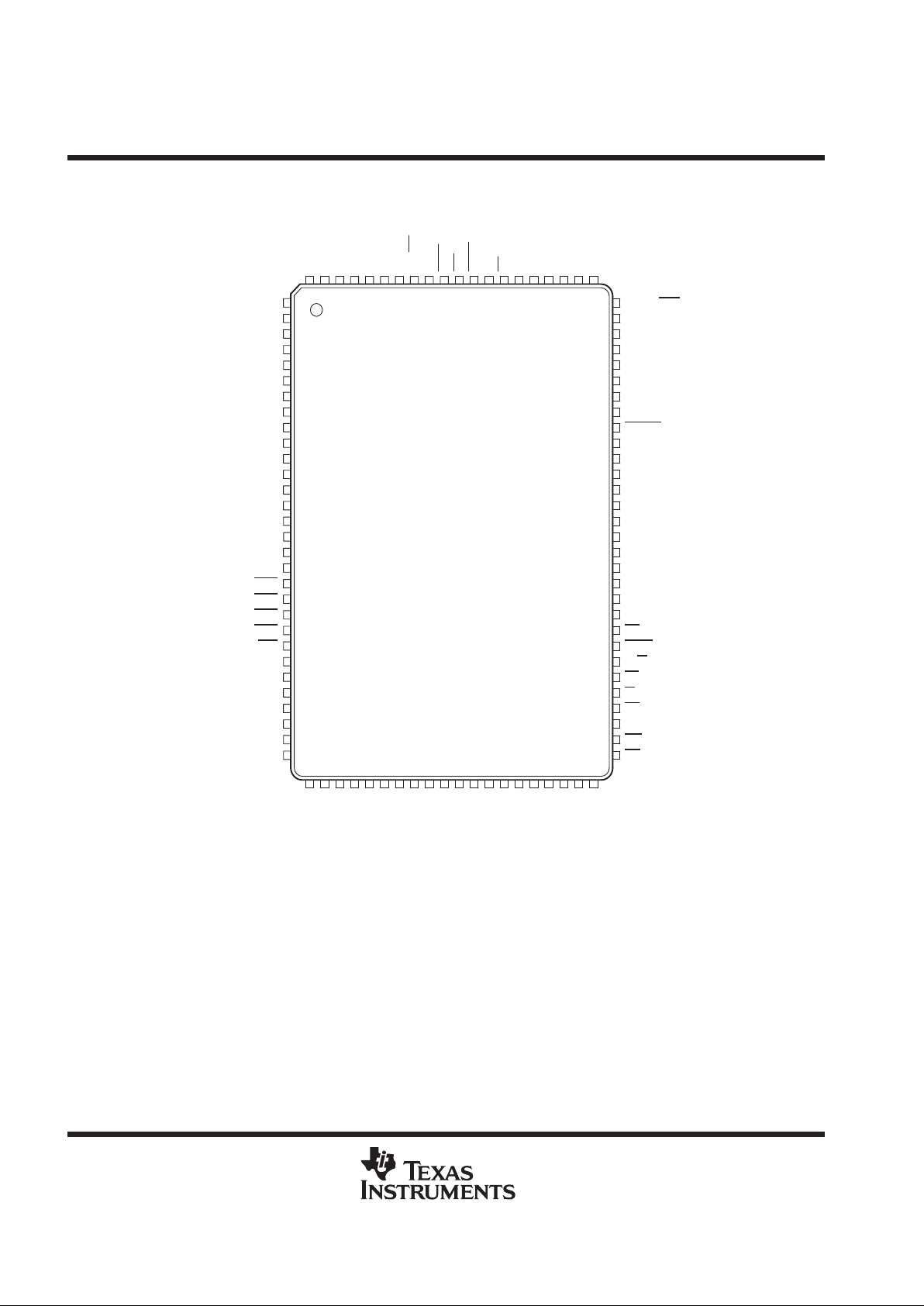
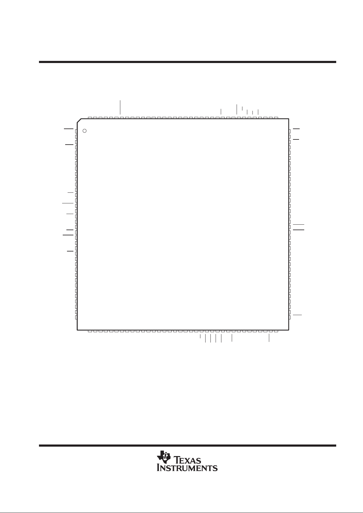
TMS320LC57
PBK PACKAGE
( TOP VIEW )
FSX
HD5
HD4
V
SSIVSSIVDDC
BR
DSVV
SSC
SSC
V
DDI
HBIL
HR/W
HCNTL0
HCNTL1
V
DDC
TMS320C5x, TMS320LC5x
DIGITAL SIGNAL PROCESSORS
SPRS030A – APRIL 1995 – REVISED APRIL 1996
7
POST OFFICE BOX 1443 • HOUSTON, TEXAS 77251–1443
Pin Functions for the TMS320LC57 in the PBK Package
SIGNAL TYPE DESCRIPTION
PARALLEL INTERFACE BUS
A0–A15 I/O/Z 16-bit external address bus (MSB: A15, LSB: A0)
D0–D15 I/O/Z 16-bit external data bus (MSB: D15, LSB: D0)
PS, DS, IS O/Z Program, data, and I/O space select outputs, respectively
STRB I/O/Z Timing strobe for external cycles and external DMA
R/W I/O/Z Read/write select for external cycles and external DMA
RD, WE O/Z Read and write strobes, respectively, for external cycles
READY I External bus ready/wait-state control input
BR I/O/Z Bus request. Arbitrates global memory and external DMA
SYSTEM INTERFACE/CONTROL SIGNALS
RS I Reset. Initializes device and sets PC to zero
MP/MC I Microprocessor/microcomputer mode select. Enables internal ROM
HOLD I Puts parallel I/F bus in high-impedance state after current cycle
HOLDA O/Z Hold acknowledge. Indicates external bus in hold state
XF O/Z External flag output. Set/cleared through software
BIO I I/O branch input. Implements conditional branches
TOUT O/Z Timer output signal. Indicates output of internal timer
IAQ O/Z Instruction acquisition signal
INT1–INT4 I External interrupt inputs
NMI I Nonmaskable external interrupt
SERIAL PORT INTERFACE
DR I Serial receive-data input
DX O/Z Serial transmit-data output. In high-impedance state when not transmitting
CLKR I Serial receive-data clock input
CLKX I/O/Z Serial transmit-data clock. Internal or external source
FSR I Serial receive-frame-synchronization input
FSX I/O/Z Serial transmit-frame-synchronization signal. Internal or external source
HOST PORT INTERFACE (HPI)
HCNTL0 I HPI mode control 1
HCNTL1 I HPI mode control 2
HINT O/Z Host interrupt
HDS1 I HPI data strobe 1
HDS2 I HPI data strobe 2
HR/W I HPI read/write strobe
HAS I HPI address strobe
HRDY O/Z HPI ready signal
HCS I HPI chip select
HBIL I HPI byte identification input
HD0–HD7 I/O/Z HPI data bus
LEGEND:
I = Input
O = Output
Z = High impedance
TMS320C5x, TMS320LC5x
DIGITAL SIGNAL PROCESSORS
SPRS030A – APRIL 1995 – REVISED APRIL 1996
8
POST OFFICE BOX 1443 • HOUSTON, TEXAS 77251–1443
Pin Functions for the TMS320LC57 in the PBK Package (Continued)
SIGNAL TYPE DESCRIPTION
BUFFERED SERIAL PORT
BDR I BSP receive data input
BDX O/Z BSP transmit data output; in high-impedance state when not transmitting
BCLKR I BSP receive-data clock input
BCLKX I/O/Z BSP transmit-data clock; internal or external source
BFSR I BSP receive frame-synchronization input
BFSX I/O/Z BSP transmit frame-synchronization signal; internal or external source
EMULATION/JTAG INTERFACE
TDI I JTAG-test-port scan data input
TDO O/Z JTAG-test-port scan data output
TMS I JTAG-test-port mode select input
TCK I JTAG-port clock input
TRST I JTAG-port reset (with pull-down resistor). Disables JTAG when low
EMU0 I/O/Z Emulation control 0. Reserved for emulation use
EMU1/OFF I/O/Z Emulation control 1. Puts outputs in high-impedance state when low
CLOCK GENERATION AND CONTROL
X1 O Oscillator output
X2/CLKIN I Clock input
CLKMD1, CLKMD2,
CLKMD3
I Clock-mode select inputs
CLKOUT1 O/Z Device system-clock output
POWER SUPPLY CONNECTIONS
V
DDA
S Supply connection, address-bus output
V
DDD
S Supply connection, data-bus output
V
DDC
S Supply connection, control output
V
DDI
S Supply connection, internal logic
V
SSA
S Supply connection, address-bus output
V
SSD
S Supply connection, data-bus output
V
SSC
S Supply connection, control output
V
SSI
S Supply connection, internal logic
LEGEND:
I = Input
O = Output
S = Supply
Z = High impedance
TMS320C5x, TMS320LC5x
DIGITAL SIGNAL PROCESSORS
SPRS030A – APRIL 1995 – REVISED APRIL 1996
9
POST OFFICE BOX 1443 • HOUSTON, TEXAS 77251–1443
INT3
INT2
INT1
HOLDA
TMS320C51, TMS320LC51, TMS320C52, TMS320LC52, TMS320C53S, TMS320LC53S, TMS320LC56
PZ PACKAGE
(TOP VIEW)
EMU1/OFF
V
SSC
RS
READY
HOLD
BIO
TRST
V
SSI
MP/MC
D15
D14
D12
D11
D10
D9
D8
V
DDD
18
25
24
23
22
21
20
19
17
16
15
14
13
12
11
10
9
8
7
6
5
4
3
2
1EMU0
TOUT
D13
V
SSI
58
51
52
53
54
55
56
57
59
60
61
62
63
64
65
66
67
68
69
70
71
72
73
7475RD
V
DDA
A15
A14
A13
A12
A11
A10
CLKMD1
V
SSA
V
SSA
V
DDI
A9
A8
A7
A5
A4
A3
A2
A1
WE
A6
TDI
A0
100 99 98 97 96 95 94 93 92 91 90 89 88 87 86 85 84 83 82 81 80 79 78 77 76
DDC
V
CLKOUT1XF†
†
CLKMD2
TDO
†
BR
R/W
DS
X1
DDIVDDI
V
SSI
V
SSI
V
DDC
V
SSC
V
STRB
PS
IS
26 27 28 29 30 31 32 33 34 35 36 37 38 39 40 41 42 43 44 45 46 47 48 49 50
SSD
V
D7
D6
D3D2D1
D0
TMS
TCK
SSD
V
DDD
V
D5
D4
INT4
NMI
†††
†
X2/CLKIN
V
SSA
†
†
†
†
†
†
DDA
V
SSDVSSD
V
†
See Table 2 for device-specific pinouts.
NOTE: NC = No connect (These pins are reserved.)
Table 2. Device-Specific Pinouts for the PZ Package
PIN ’C51, ’LC51 ’C52, ’LC52 ’C53S, ’LC53S ’LC56
‡
5 TCLKX V
SSI
CLKX2 BCLKX
6
§
CLKX CLKX CLKX1 CLKX
7 TFSR/TADD V
SSI
FSR2 BFSR
8 TCLKR V
SSI
CLKR2 BCLKR
46
§
DR DR DR1 DR
47 TDR V
SSI
DR2 BDR
48
§
FSR FSR FSR1 FSR
49
§
CLKR CLKR CLKR1 CLKR
83 CLKIN2 CLKIN2 CLKIN2 CLKMD3
91
§
FSX FSX FSX1 FSX
92 TFSX/TFRM V
SSI
FSX2 BFSX
93
§
DX DX DX1 DX
94 TDX NC DX2 BDX
‡
Pin names beginning with “B” indicate signals on the buffered serial port (BSP).
§
No functional change
TMS320C5x, TMS320LC5x
DIGITAL SIGNAL PROCESSORS
SPRS030A – APRIL 1995 – REVISED APRIL 1996
10
POST OFFICE BOX 1443 • HOUSTON, TEXAS 77251–1443
Pin Functions for Devices in the PZ Package
SIGNAL TYPE DESCRIPTION
PARALLEL INTERFACE BUS
A0–A15 I/O/Z 16-bit external address bus (MSB: A15, LSB: A0)
D0–D15 I/O/Z 16-bit external data bus (MSB: D15, LSB: D0)
PS, DS, IS O/Z Program, data, and I/O space select outputs, respectively
STRB I/O/Z Timing strobe for external cycles and external DMA
R/W I/O/Z Read/write select for external cycles and external DMA
RD, WE O/Z Read and write strobes, respectively, for external cycles
READY I External bus ready/wait-state control input
BR I/O/Z Bus request. Arbitrates global memory and external DMA
SYSTEM INTERFACE/CONTROL SIGNALS
RS I Reset. Initializes device and sets PC to zero
MP/MC I Microprocessor/microcomputer mode select. Enables internal ROM
HOLD I Puts parallel I/F bus in high-impedance state after current cycle
HOLDA O/Z Hold acknowledge. Indicates external bus in hold state
XF O/Z External flag output. Set/cleared through software
BIO I I/O branch input. Implements conditional branches
TOUT O/Z Timer output signal. Indicates output of internal timer
INT1–INT4 I External interrupt inputs
NMI I Nonmaskable external interrupt
SERIAL PORT INTERFACE
DR, DR1, DR2 I Serial receive-data input
DX, DX1, DX2 O/Z Serial transmit-data output. In high-impedance state when not transmitting
CLKR, CLKR1, CLKR2 I Serial receive-data clock input
CLKX, CLKX1, CLKX2 I/O/Z Serial transmit-data clock. Internal or external source
FSR, FSR1, FSR2 I Serial receive-frame-synchronization input
FSX, FSX1, FSX2 I/O/Z Serial transmit-frame-synchronization signal. Internal or external source
BUFFERED SERIAL PORT (BSP) (SEE NOTE 1)
BDR I BSP receive data input
BDX O/Z BSP transmit data output; in high-impedance state when not transmitting
BCLKR I BSP receive-data clock input
BCLKX I/O/Z BSP transmit-data clock; internal or external source
BFSR I BSP receive frame-synchronization input
BFSX I/O/Z BSP transmit frame-synchronization signal; internal or external source
LEGEND:
I = Input
O = Output
Z = High impedance
NOTE 1: ’LC56 devices only
TMS320C5x, TMS320LC5x
DIGITAL SIGNAL PROCESSORS
SPRS030A – APRIL 1995 – REVISED APRIL 1996
11
POST OFFICE BOX 1443 • HOUSTON, TEXAS 77251–1443
Pin Functions for Devices in the PZ Package (Continued)
SIGNAL TYPE DESCRIPTION
TDM SERIAL PORT INTERFACE
TDR I TDM serial receive-data input
TDX O/Z TDM serial transmit-data output. In high-impedance state when not transmitting
TCLKR I TDM serial receive-data clock input
TCLKX I/O/Z TDM serial transmit-data clock. Internal or external source
TFSR / TADD I/O/Z
TDM serial receive-frame-synchronization input. In the TDM mode, TFSR/TADD is used to output/
input the address of the port
TFSX /TFRM I
TDM serial transmit-frame-synchronization signal. Internal or external source. In the TDM mode,
TFSX/TFRM becomes TFRM, the TDM frame sync.
EMULATION/JTAG INTERFACE
TDI I JTAG-test-port scan data input
TDO O/Z JTAG-test-port scan data output
TMS I JTAG-test-port mode select input
TCK I JTAG-port clock input
TRST I JTAG-port reset (with pull-down resistor). Disables JTAG when low
EMU0 I/O/Z Emulation control 0. Reserved for emulation use
EMU1/OFF I/O/Z Emulation control 1. Puts outputs in high-impedance state when low
CLOCK GENERATION AND CONTROL (SEE NOTE 2)
X1 O Oscillator output
X2/CLKIN I Clock/oscillator input (PLL clock input for ’C56)
CLKIN2 I Clock input (PLL clock input for ’C50, ’C51, ’C52, ’C53, ’C53S)
CLKMD1, CLKMD2,
CLKMD3
I Clock-mode select inputs
CLKOUT1 O/Z Device system-clock output
POWER SUPPLY CONNECTIONS
V
DDA
S Supply connection, address-bus output
V
DDD
S Supply connection, data-bus output
V
DDC
S Supply connection, control output
V
DDI
S Supply connection, internal logic
V
SSA
S Supply connection, address-bus output
V
SSD
S Supply connection, data-bus output
V
SSC
S Supply connection, control output
V
SSI
S Supply connection, internal logic
LEGEND:
I = Input
O = Output
S = Supply
Z = High impedance
NOTE 2: CLKIN2 pin is replaced by CLKMD3 pin on ’LC56 devices.
TMS320C5x, TMS320LC5x
DIGITAL SIGNAL PROCESSORS
SPRS030A – APRIL 1995 – REVISED APRIL 1996
12
POST OFFICE BOX 1443 • HOUSTON, TEXAS 77251–1443
D8
V
DDD
V
SSD
V
SSD
D7
D6
D5
D4
D3
D2
D1
D0
TMS
V
DDD
V
DDD
TCK
V
SSD
V
SSD
INT1
INT2
INT3
INT4
NMI
DR
V
SSI
FSR
CLKR
V
DDA
V
SSA
A0
100
31 32 33 34 35 36 37 38 39 40 41 42 43 44 45 46 47 48 49 50
99
98
97 96 95
94 93 92
91 90 89
88 87
86 85 84
83 82
81
SSA
A2A3A4
A5A1A7A8A9
A6
DDI
TDI
CLKMD1
A11
A12
A13
A14
A10
A15
MP/MC
D10
D11
D12
D13D9D14
V
TRST
CLKX
HOLD
READY
BIO
RSVV
TOUT
V
V
D15
TMS320C52, TMS320LC52
PJ PACKAGE
(TOP VIEW)
DDA
SSI
SSI
SSI
SSC
SSI
EMU1/OFF
EMU0
V
DDC
V
DDC
V
DDI
V
DDI
CLKOUT1
XF
HOLDA
NC
DX
V
SSI
FSX
CLKMD2
V
SSI
V
SSI
TDO
V
DDC
X1
X2/CLKIN
CLKIN2
BR
STRB
R/W
PS
IS
DS
V
SSC
WE
RD
V
V
V
1
2
3
4
5
6
7
8
9
10
11
12
13
14
15
16
17
18
19
20
21
22
23
24
25
26
27
28
29
30
80
79
78
77
76
75
74
73
72
71
70
69
68
67
66
65
64
63
62
61
60
59
58
57
56
55
54
53
52
51
NOTE: NC = No connect (These pins are reserved.)
TMS320C5x, TMS320LC5x
DIGITAL SIGNAL PROCESSORS
SPRS030A – APRIL 1995 – REVISED APRIL 1996
13
POST OFFICE BOX 1443 • HOUSTON, TEXAS 77251–1443
Pin Functions for the TMS320C52, TMS320LC52 in the PJ Package
SIGNAL TYPE DESCRIPTION
PARALLEL INTERFACE BUS
A0–A15 I/O/Z 16-bit external address bus (MSB: A15, LSB: A0)
D0–D15 I/O/Z 16-bit external data bus (MSB: D15, LSB: D0)
PS, DS, IS O/Z Program, data, and I/O space select outputs, respectively
STRB I/O/Z Timing strobe for external cycles and external DMA
R/W I/O/Z Read/write select for external cycles and external DMA
RD, WE O/Z Read and write strobes, respectively, for external cycles
READY I External bus ready/wait-state control input
BR I/O/Z Bus request. Arbitrates global memory and external DMA
SYSTEM INTERFACE/CONTROL SIGNALS
RS I Reset. Initializes device and sets PC to zero
MP/MC I Microprocessor/microcomputer mode select. Enables internal ROM
HOLD I Puts parallel I/F bus in high-impedance state after current cycle
HOLDA O/Z Hold acknowledge. Indicates external bus in hold state
XF O/Z External flag output. Set/cleared through software
BIO I I/O branch input. Implements conditional branches
TOUT O/Z Timer output signal. Indicates output of internal timer
INT1–INT4 I External interrupt inputs
NMI I Nonmaskable external interrupt
SERIAL PORT INTERFACE
DR I Serial receive-data input
DX O/Z Serial transmit-data output. In high-impedance state when not transmitting
CLKR I Serial receive-data clock input
CLKX I/O/Z Serial transmit-data clock. Internal or external source
FSR I Serial receive-frame-synchronization input
FSX I/O/Z Serial transmit-frame-synchronization signal. Internal or external source
EMULATION/JTAG INTERFACE
TDI I JTAG-test-port scan data input
TDO O/Z JTAG-test-port scan data output
TMS I JTAG-test-port mode select input
TCK I JTAG-port clock input
TRST I JTAG-port reset (with pulldown resistor). Disables JTAG when low
EMU0 I/O/Z Emulation control 0. Reserved for emulation use
EMU1/OFF I/O/Z Emulation control 1. Puts outputs in high-impedance state when low
LEGEND:
I = Input
O = Output
Z = High impedance
TMS320C5x, TMS320LC5x
DIGITAL SIGNAL PROCESSORS
SPRS030A – APRIL 1995 – REVISED APRIL 1996
14
POST OFFICE BOX 1443 • HOUSTON, TEXAS 77251–1443
Pin Functions for the TMS320C52, TMS320LC52 in the PJ Package (Continued)
SIGNAL TYPE DESCRIPTION
CLOCK GENERATION AND CONTROL
X1 O Oscillator output
X2/CLKIN I Clock/oscillator input
CLKIN2 I Clock input (PLL clock input for ’C52, ’LC52)
CLKMD1, CLKMD2 I Clock-mode select inputs
CLKOUT1 O/Z Device system-clock output
POWER SUPPLY CONNECTIONS
V
DDA
S Supply connection, address-bus output
V
DDD
S Supply connection, data-bus output
V
DDC
S Supply connection, control output
V
DDI
S Supply connection, internal logic
V
SSA
S Supply connection, address-bus output
V
SSD
S Supply connection, data-bus output
V
SSC
S Supply connection, control output
V
SSI
S Supply connection, internal logic
LEGEND:
I = Input
O = Output
S = Supply
TMS320C5x, TMS320LC5x
DIGITAL SIGNAL PROCESSORS
SPRS030A – APRIL 1995 – REVISED APRIL 1996
15
POST OFFICE BOX 1443 • HOUSTON, TEXAS 77251–1443
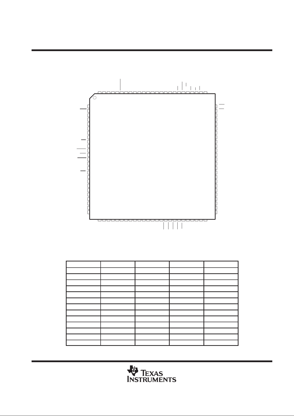
TMS320C57S, TMS320LC57S
PGE PACKAGE
(TOP VIEW)
TDO
WE
HD1
RD
HD0
HRDY
V
DDA
A15
NC
A14
A13
A12
NC
A11
A10
CLKMD1
V
SSA
V
SSA
TDI
HDS1
HDS2
V
DDI
V
DDI
A9
A8
A7
NC
A6
A5
A4
A3
NC
A2
A1
A0
V
SSA
HCS
HINT
EMU0
NC
EMU1/OFF
V
SSC
V
SSC
TOUT
BCLKX
CLKX
V
DDC
BFSR
BCLKR
RS
READY
HOLD
NC
BIO
V
DDC
V
DDC
IAQ
TRST
V
SSI
V
SSI
MP/MC
D15
D14
D13
NC
D12
D11
D10
D9
NC
D8
V
DDD
V
DDD
144
143
142
CLKOUT1
141XF140
139
BDX
138
137
136
BFSX
135
134
133
HD5
132
CLKMD2
131
130
129
128
127
126
125
X2/CLKIN
124
CLKMD3
123
122
HD3
121
STRB
120
119
PS
118
117
116
115
114
113
112
373839404142434445464748495051525354555657585960616263646566676869
1
2
3
4
5
6
7
8
9
10
11
12
13
14
15
16
17
18
19
20
21
22
23
24
25
26
27
28
29
30
31
32
33
34
35
36
108
107
106
105
104
103
102
101
100
99
98
97
96
95
94
93
92
91
90
89
88
87
86
85
84
83
82
81
80
79
78
77
76
75
74
73
D7
D6
D5
D3
D2
D1
HCNTL0
TMS
NMI
HR/W
INT2
INT3
INT4
DR
BDR
FSR
HAS
HCNTL1
111
NC
110
109
707172
NC
TCK
HD6
DX
V
SSI
HD4
V
DDC
DDD
V
CLKR
DDA
V
HBIL
SSD
V
D4
D0
INT1
NC
V
DDCVDDI
V
HOLDA
HD7
FSX
V
SSI
X1
BR
R/W
IS
DS
HD2
V
SSC
V
SSC
NC
NC
NC
SSD
V
DDI
SSD
V
DDD
V
SSD
V
DDA
V
NOTE: NC = No connect (These pins are reserved.)
NC
NC
ADVANCE INFORMATION

TMS320C5x, TMS320LC5x
DIGITAL SIGNAL PROCESSORS
SPRS030A – APRIL 1995 – REVISED APRIL 1996
16
POST OFFICE BOX 1443 • HOUSTON, TEXAS 77251–1443
Pin Functions for the TMS320C57S, TMS320LC57S in the PGE Package
SIGNAL TYPE DESCRIPTION
PARALLEL INTERFACE BUS
A0–A15 I/O/Z 16-bit external address bus (MSB: A15, LSB: A0)
D0–D15 I/O/Z 16-bit external data bus (MSB: D15, LSB: D0)
PS, DS, IS O/Z Program, data, and I/O space select outputs, respectively
STRB I/O/Z Timing strobe for external cycles and external DMA
R/W I/O/Z Read/write select for external cycles and external DMA
RD, WE O/Z Read and write strobes, respectively, for external cycles
READY I External bus ready/wait-state control input
BR I/O/Z Bus request. Arbitrates global memory and external DMA
SYSTEM INTERFACE/CONTROL SIGNALS
RS I Reset. Initializes device and sets PC to zero
MP/MC I Microprocessor/microcomputer mode select. Enables internal ROM
HOLD I Puts parallel I/F bus in high-impedance state after current cycle
HOLDA O/Z Hold acknowledge. Indicates external bus in hold state
XF O/Z External flag output. Set/cleared through software
BIO I I/O branch input. Implements conditional branches
TOUT O/Z Timer output signal. Indicates output of internal timer
IAQ O/Z Instruction acquisition signal
INT1–INT4 I External interrupt inputs
NMI I Nonmaskable external interrupt
SERIAL PORT INTERFACE (SPI)
DR I Serial receive-data input
DX O/Z Serial transmit-data output. In high-impedance state when not transmitting
CLKR I Serial receive-data clock input
CLKX I/O/Z Serial transmit-data clock. Internal or external source
FSR I Serial receive-frame-synchronization input
FSX I/O/Z Serial transmit-frame-synchronization signal. Internal or external source
HOST PORT INTERFACE (HPI)
HCNTL0 I HPI mode control 1
HCNTL1 I HPI mode control 2
HINT O/Z Host interrupt
HDS1 I HPI data strobe 1
HDS2 I HPI data strobe 2
HR/W I HPI read/write strobe
HAS I HPI address strobe
HRDY O/Z HPI ready signal
HCS I HPI chip select
HBIL I HPI byte identification input
HD0–HD7 I/O/Z HPI data bus
LEGEND:
I = Input
O = Output
Z = High impedance
TMS320C5x, TMS320LC5x
DIGITAL SIGNAL PROCESSORS
SPRS030A – APRIL 1995 – REVISED APRIL 1996
17
POST OFFICE BOX 1443 • HOUSTON, TEXAS 77251–1443
Pin Functions for the TMS320C57S, TMS320LC57S in the PGE Package (Continued)
SIGNAL TYPE DESCRIPTION
BUFFERED SERIAL PORT
BDR I BSP receive data input
BDX O/Z BSP transmit data output; in high-impedance state when not transmitting
BCLKR I BSP receive-data clock input
BCLKX I/O/Z BSP transmit-data clock; internal or external source
BFSR I BSP receive frame-synchronization input
BFSX I/O/Z BSP transmit frame-synchronization signal; internal or external source
EMULATION/JTAG INTERFACE
TDI I JTAG-test-port scan data input
TDO O/Z JTAG-test-port scan data output
TMS I JTAG-test-port mode select input
TCK I JTAG-port clock input
TRST I JTAG-port reset (with pulldown resistor). Disables JTAG when low
EMU0 I/O/Z Emulation control 0. Reserved for emulation use
EMU1/OFF I/O/Z Emulation control 1. Puts outputs in high-impedance state when low
CLOCK GENERATION AND CONTROL
X1 O Oscillator output
X2/CLKIN I PLL clock input
CLKMD1, CLKMD2,
CLKMD3
I Clock-mode select inputs
CLKOUT1 O/Z Device system-clock output
POWER SUPPLY CONNECTIONS
V
DDA
S Supply connection, address-bus output
V
DDD
S Supply connection, data-bus output
V
DDC
S Supply connection, control output
V
DDI
S Supply connection, internal logic
V
SSA
S Supply connection, address-bus output
V
SSD
S Supply connection, data-bus output
V
SSC
S Supply connection, control output
V
SSI
S Supply connection, internal logic
LEGEND:
I = Input
O = Output
S = Supply
Z = High impedance

TMS320C5x, TMS320LC5x
DIGITAL SIGNAL PROCESSORS
SPRS030A – APRIL 1995 – REVISED APRIL 1996
18
POST OFFICE BOX 1443 • HOUSTON, TEXAS 77251–1443
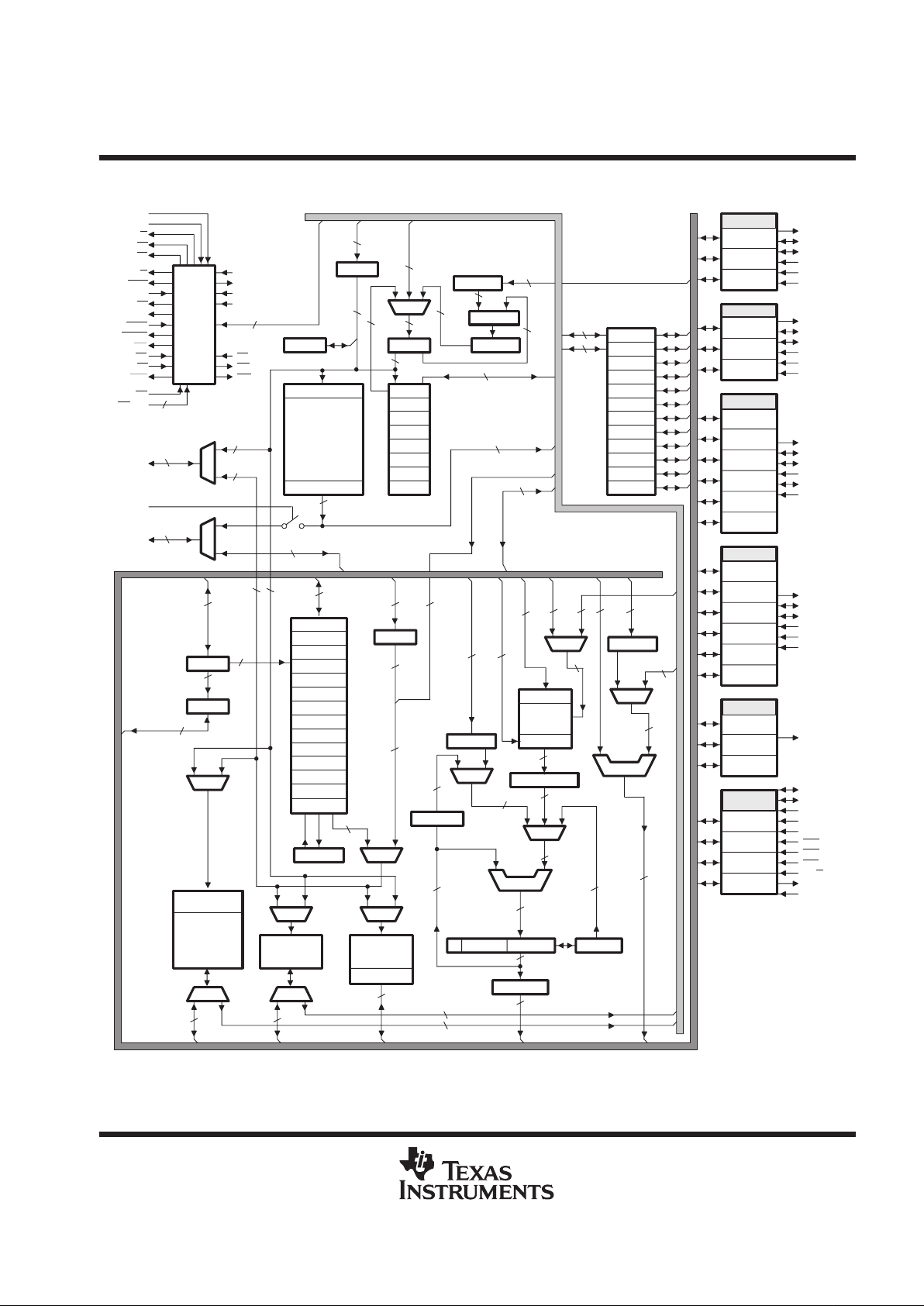
architecture
The ’C5x’s advanced Harvard-type architecture maximizes the processing power by maintaining two separate
memory bus structures, program and data, for full-speed execution. Instructions support data transfers between
the two spaces. This architecture permits coefficients stored in program memory to be read into the RAM,
eliminating the need for a separate coefficient ROM. The ’C5x architecture also makes available immediate
instructions and subroutines based on computed values. Increased throughput on the ’C5x for many DSP
applications is accomplished using single-cycle multiply/accumulate instructions with a data-move option, up
to eight auxiliary registers with a dedicated arithmetic unit, a parallel logic unit, and faster I/O necessary for
data-intensive signal processing. The architectural design emphasizes overall speed, communication, and
flexibility in processor configuration. Control signals and instructions provide floating-point support,
block-memory transfers, communication to slower off-chip devices, and multiprocessing implementations
as shown in the functional block diagram.
Table 3 explains the symbols that are used in the functional block diagram.
Table 3. Symbols Used in Functional Block Diagram
SYMBOL DESCRIPTION SYMBOL DESCRIPTION
ABU Auto-buffering unit IFR Interrupt-flag register
ACCB Accumulator buffer IMR Interrupt-mask register
ACCH Accumulator high INDX Indirect-addressing-index register
ACCL Accumulator low IR Instruction register
ALU Arithmetic logic unit MCS Microcall stack
ARAU Auxiliary-register arithmetic unit MUX Multiplexer
ARB Auxiliary-register pointer buffer PAER Block-repeat-address end register
ARCR Auxiliary-register compare register PASR Block-repeat-address start register
ARP Auxiliary-register pointer PC Program counter
ARR Address-receive register (ABU) PFC Prefetch counter
AR0–AR7 Auxiliary registers PLU Parallel logic unit
AXR Address-transmit register (ABU) PMST Processor-mode-status register
BKR Receive-buffer-size register (ABU) PRD Timer-period register
BKX Transmit-buffer-size register (ABU) PREG Product register
BMAR Block-move-address register RPTC Repeat-counter register
BRCR Block-repeat-counter register SARAM Single-access RAM
BSP Buffered serial port SFL Left shifter
C Carry bit SFR Right shifter
CBER1 Circular buffer 1 end address SPC Serial-port interface-control register
CBER2 Circular buffer 2 end address ST0,ST1 Status registers
CBSR1 Circular buffer 1 start address TCSR TDM channel-select register
CBSR2 Circular buffer 2 start address TCR Timer-control register
DARAM Dual-access RAM TDM Time-division-multiplexed serial port
DBMR Dynamic bit manipulation register TDXR TDM data transmit register
DP Data memory page pointer TIM Timer-count register
DRR Serial-port data receive register TRAD TDM received-address register
DXR Serial-port data transmit register TRCV TDM data-receive register
GREG Global memory allocation register TREG0 Temporary register for multiplication
HPI Host port interface TREG1 Temporary register for dynamic shift count
HPIAH HPI-address register (high bytes) TREG2 Temporary register used as bit pointer in dynamic-bit test
HPIAL HPI-address register (low bytes) TRTA TDM receive-/transmit-address register
HPICH HPI-control register (high bytes) TSPC TDM serial-port-control register
HPICL HPI-control register (low bytes)
TMS320C5x, TMS320LC5x
DIGITAL SIGNAL PROCESSORS
SPRS030A – APRIL 1995 – REVISED APRIL 1996
19
POST OFFICE BOX 1443 • HOUSTON, TEXAS 77251–1443
functional block diagram
32
16
Data Bus
Program Bus
16
16
Shifter(0–7)
D15–D0
RBIT
A15–A0
16
16
16
16
DBMR(16)
MUX
16 16
32
ACCB(32)
32
ACCL(16)ACCH(16)C
32
ALU(32)
32
SFR(0–16)
32
MUX
MUX
SFL(0–16)
16
MUX
PREG(32)
Multiplier
TREG0(16)
MUX
16
16
16
MUX
B1 (512x16)
B2 (32x16)
DARAM
B0 (512x16)
DARAM
MUX
from IR
7 LSB
MUX
DP(9)
9
9
MUX
16
’C50 9K
’C51 1K
’C53 3K
’C56 6K
’C57 6K
SARAM
16
ARAU(16)
16
MUX
3
3
3
3
ARB(3)
ARP(3)
Program Bus
16
16
16
16
CBSR2(16)
CBSR1(16)
AR7(16)
AR6(16)
AR5(16)
AR3(16)
AR2(16)
AR1(16)
AR0(16)
ARCR(16)
INDX(16)
HDS(1–1)
HRDY
HAS
HR/W
HINT
HPI
HPICL
HD7
HD0
HBIL
HCNTL0
HCNTL1
HCSHPIAL
HPICH
HPIAH
TOUT
TCR
PRD
TIM
Timer
BDX
BCLKX
BDR
BCLKR
BFSR
DFSX
DXR
AXR(11)
BKX(11)
DRR
ARR(11)
BKR(11)
BSP
TDM
TCSR(8)
TRTA
TRAD(16)
TDR
TCLKX
TFRM
TADD
TCLKR
TRCV
TDXR
TSPC
TDX
CLKX2
FSX2
DX2
FSR2
CLKR2
DR2
SPC
DXR
DRR
Serial Port 2
CLKR
FSR
DR
FSX
CLKX
DX
DRR
DXR
SPC
Serial Port 1
16
16
TREG2(4)
TREG1(5)
BRCR(16)
GREG(16)
IFR(16)
IMR(16)
RPTC(16)
PMST(16)
ST1(16)
ST0(16)
BMAR(16)
IR(16)
16
16
16
16
16
PFC(16)
MCS(16)
Instruction
Address
32K’C57
32K’C56
16K’C53
4K’C52
8K’C51
2K’C50
ROMProgram
16
16
16
16
16
PASR(16)
Compare
PAER(16)
(8x16)
Stack
PC(16)
16
MUX
NMI
WE
RD
16
CLKIN2/CLKMD3
X2/CLKIN
CLKOUT1
X1
4
INT(1–4)
MP/MC
IACK
RS
HOLDA
HOLD
XF
BR
READY
STRB
RW
PS
DS
IS
CLKMD2
CLKMD1
Control
Data Bus
Program Bus
Data Bus
Data Bus
CBER2(16)
CBER1(16)
AR4(16)
16
BO
IAQ
†
†
†
†
MUXMUX
Data/Prog
Data/Prog
16
SFL (–6,0,1, 4)
PLU (16)
16
Data
32
16
16
16
16
16
16
32
32
16
†
Not available on all devices (see Table 1).
NOTES: A. Signals in shaded text are not available on
100-pin QFP packages.
B. Symbol descriptions appear in Table 3.

TMS320C5x, TMS320LC5x
DIGITAL SIGNAL PROCESSORS
SPRS030A – APRIL 1995 – REVISED APRIL 1996
20
POST OFFICE BOX 1443 • HOUSTON, TEXAS 77251–1443
32-bit ALU/accumulator
The 32-bit ALU and accumulator implement a wide range of arithmetic and logical functions, the majority of
which execute in a single cycle. The ALU is a general-purpose arithmetic/logic unit that operates on 16-bit words
taken from data memory or derived from immediate instructions. In addition to the usual arithmetic instructions,
the ALU can perform Boolean operations, facilitating the bit manipulation ability required of a high-speed
controller. One input to the ALU always is supplied by the accumulator, and the other input can be furnished
from the product register (PREG) of the multiplier, the accumulator buf fer (ACCB), or the output of the scaling
shifter [which has been read from data memory or from the accumulator (ACC)]. After the ALU performs the
arithmetic or logical operation, the result is stored in the ACC where additional operations, such as shifting, can
be performed. Data input to the ALU can be scaled by the scaling shifter. The 32-bit ACC is split into two 16-bit
segments for storage in data memory . Shifters at the output of the ACC provide a left shift of 0 to 7 places. This
shift is performed while the data is being transferred to the data bus for storage. The contents of the ACC remain
unchanged. When the postscaling shifter is used on the high word of the ACC (bits 31–16), the most significant
bits (MSBs) are lost and the least significant bits (LSBs) are filled with bits shifted in from the low word (bits
15–0). When the postscaling shifter is used on the low word, the LSBs are filled with zeros.
The ’C5x supports floating-point operations for applications requiring a large dynamic range. By performing left
shifts, the normalization instruction (NORM) is used to normalize fixed-point numbers contained in the ACC.
The four bits of the TREG1 define a variable shift through the scaling shifter for the ADDT/LACT/SUBT
instructions (add to/load to/subtract from ACC with shift specified by TREG1). These instructions are useful
in denormalizing a number (converting from floating point to fixed point). They are also useful for executing an
automatic gain control (AGC) going into a filter.
The single-cycle 1-bit to 16-bit right shift of the ACC efficiently aligns the ACC’s contents. This, coupled with
the 32-bit temporary buffer on the ACC, enhances the effectiveness of the ALU in extended-precision arithmetic.
The ACCB provides a temporary storage place for a fast save of the ACC. The ACCB also can be used as an
input to the ALU. The minimum or maximum value in a string of numbers is found by comparing the contents
of the ACCB with the contents of the ACC. The minimum or maximum value is placed in both registers, and,
if the condition is met, the carry bit (C) is set to 1. The minimum and maximum functions are executed by the
CRLT and CRGT instructions, respectively.
scaling shifters
The ’C5x provides a scaling shifter that has a 16-bit input connected to the data bus and a 32-bit output
connected to the ALU. This scaling shifter produces a left shift of 0 to 16 bits on the input data. The shift count
is specified by a constant embedded in the instruction word or by the value in TREG1. The LSBs of the output
are filled with zeros; the MSBs may be either filled with zeros or sign extended, depending upon the value of
the sign-extension mode (SXM) bit of status register ST1.
The ’C5x also contains several other shifters that allow it to perform numerical scaling, bit extraction,
extended-precision arithmetic, and overflow prevention. These shifters are connected to the output of the
product register and the ACC.
parallel logic unit
The parallel logic unit (PLU) is a second logic unit, additional to the main ALU, that executes logic operations
on data without affecting the contents of the ACC. The PLU provides the bit-manipulation ability required of a
high-speed controller and simplifies control/status register operations. The PLU provides a direct logic
operation path to data memory space and can set, clear, test, or toggle multiple bits directly in a data memory
location, a control/status register, or any register that is mapped into data memory space.

TMS320C5x, TMS320LC5x
DIGITAL SIGNAL PROCESSORS
SPRS030A – APRIL 1995 – REVISED APRIL 1996
21
POST OFFICE BOX 1443 • HOUSTON, TEXAS 77251–1443
16 × 16-bit parallel multiplier
The ’C5x uses a 16 × 16-bit hardware multiplier that is capable of computing a signed or an unsigned 32-bit
product in a single machine cycle. All multiply instructions, except the MPYU (multiply unsigned) instruction,
perform a signed multiply operation in the multiplier. That is, two numbers being multiplied are treated as
2s-complement numbers, and the result is a 32-bit 2s-complement number.
There are two registers associated with the multiplier: TREG0, a 16-bit temporary register that holds one of the
operands for the multiplier, and PREG, the 32-bit product register that holds the product. Four product shift
modes (PM) are available at the PREG’s output. These shift modes are useful for performing
multiply/accumulate operations, performing fractional arithmetic, or justifying fractional products. The PM field
of status register ST1 specifies the PM shift mode.
The product can be shifted one bit to compensate for the extra sign bit gained in multiplying two 16-bit
2s-complement numbers (MPY). A 4-bit shift is used in conjunction with the MPY instruction with a short
immediate value (13 bits or less) to eliminate the four extra sign bits gained in multiplying a 16-bit number by
a 13-bit number. Finally, the output of PREG can, instead, be right-shifted 6 bits to enable the execution of up
to 128 consecutive multiply/accumulates without the possibility of overflow.
The load-TREG0 (L T) instruction normally loads TREG0 to provide one operand (from the data bus), and the
MPY instruction provides the second operand (also from the data bus). A multiplication also can be performed
with a short or long immediate operand by using the MPY instruction with an immediate operand. A product is
obtained every two cycles except when a long immediate operand is used.
Four multiply/accumulate instructions (MAC, MACD, MADD, and MADS as defined in Table 7) fully utilize the
computational bandwidth of the multiplier, allowing both operands to be processed simultaneously. The data
for these operations is transferred to the multiplier during each cycle through the program and data buses. This
facilitates single-cycle multiply/accumulates when used with repeat ( RPT and RPTZ ) instructions. In these
instructions, the coefficient addresses are generated by the PC, while the data addresses are generated by the
ARAU. This allows the repeated instruction to access the values sequentially from the coefficient table and step
through the data in any of the indirect addressing modes. The RPTZ instruction also clears the accumulator and
the product register to initialize the multiply/accumulate operation.
The MACD and MADD instructions, when repeated, support filter constructs (weighted running averages) so
that as the sum-of-products is executed, the sample data is shifted in memory to make room for the next sample
and to eliminate the oldest sample. Circular addressing with MAC and MADS instructions also can be used to
support filter implementation.
auxiliary registers and auxiliary-register arithmetic unit (ARAU)
The ’C5x provides a register file containing eight auxiliary registers (AR0–AR7). The auxiliary registers are used
for indirect addressing of the data memory or for temporary data storage. Indirect auxiliary-register addressing
allows placement of the data memory address of an instruction operand into one of the auxiliary registers. These
registers are referenced with a 3-bit auxiliary register pointer (ARP) that is loaded with a value from 0 through
7, designated AR0 through AR7, respectively. The auxiliary registers and the ARP can be loaded from data
memory , the ACC, the product register , or by an immediate operand defined in the instruction. The contents of
these registers can be stored in data memory or used as inputs to the central arithmetic logic unit (CALU). These
registers are accessible as memory-mapped locations within the ’C5x data-memory space.
The auxiliary register file (AR0–AR7) is connected to the auxiliary register arithmetic unit (ARAU). The ARAU
can autoindex the current auxiliary register while the data memory location is being addressed. Indexing can
be performed either by ±1 or by the contents of the INDX register. As a result, accessing tables of information
does not require the CALU for address manipulation; thus, the CALU is free for other operations in parallel.
TMS320C5x, TMS320LC5x
DIGITAL SIGNAL PROCESSORS
SPRS030A – APRIL 1995 – REVISED APRIL 1996
22
POST OFFICE BOX 1443 • HOUSTON, TEXAS 77251–1443
memory
The ’C5x implements three separate address spaces for program memory , data memory , and I/O. Each space
accommodates a total of 64K 16-bit words (see Figures 1 through 7). Within the 64K words of data space, the
256 to 32K words at the top of the address range can be defined to be external global memory in increments
of powers of two, as specified by the contents of the global memory allocation register (GREG). Access to global
memory is arbitrated using the global memory bus request (BR
) signal.
The ’C5x devices include a considerable amount of on-chip memory to aid in system performance and
integration including ROM, single-access RAM (SARAM), and dual-access RAM (DARAM). The amount and
types of memory available on each device are shown in Table 1.
On the ’C5x, the first 96 (0 – 5Fh) data-memory locations are allocated for memory-mapped registers. This
memory-mapped register space contains various control and status registers including those for the CPU, serial
port, timer, and software wait-state generators. Additionally, the first 16 I/O port locations are mapped into this
data-memory space, allowing them to be accessed either as data memory using single-word instructions or as
I/O locations with two-word instructions. Two-word instructions allow access to the full 64K words of I/O space.
The mask-programmable ROM is located in program memory space. Customers can arrange to have this ROM
programmed with contents unique to to any particular application. The ROM is enabled or disabled by the state
of the MP/MC
control input upon resetting the device or by manipulating the MP/MC bit in the PMST status
register after reset. The ROM occupies the lowest block of program memory when enabled. When disabled,
these addresses are located in the device’s external program-memory space.
The ’C5x also has a mask-programmable option that provides security protection for the contents of on-chip
ROM. When this internal option bit is programmed, no externally-originating instruction can access the on-chip
ROM. This feature can be used to provide security for proprietary algorithms.
An optional boot loader is available in the device’s on-chip ROM. This boot loader can be used to transfer a
program automatically from data memory or the serial port to anywhere in program memory . In data memory,
the program can be located on any 1K-word boundary and can be in either byte-wide or 16-bit word format. Once
the code is transferred, the boot loader releases control to the program for execution.
The ’C5x devices provide two types of RAM: single-access RAM (SARAM) and dual-access RAM (DARAM).
The single-access RAM requires a full machine cycle to perform a read or a write; however, this is not one large
RAM block in which only one access per cycle is allowed. It is made up of 2K-word size-independent RAM blocks
and each one allows one CPU access per cycle. The CPU can read or write one block while accessing another
block at the same time. All ’C5x processors support multiple accesses to its SARAM in one cycle as long as they
go to different RAM blocks. If the total SARAM size is not a multiple of two, one block is made smaller than 2K
words. With an understanding of this structure, programmers can arrange code and data appropriately to
improve code performance. Table 4 shows the sizes of available SARAM on the applicable ’C5x devices.
T able 4. SARAM Block Sizes
DEVICE NUMBER OF SARAM BLOCKS
’C50/’LC50 Four 2K blocks and one 1K block
’C51/’LC51 One 1K block
’C53/’C53S /’LC53 One 2K block and one 1K block
’LC56 Three 2K blocks
’C57S/’LC57/’LC57S Three 2K blocks
memory (continued)
The ’C5x dual-access RAM (DARAM) allows writes to, and reads from, the RAM in the same cycle without the
address restrictions of the SARAM. The dual-access RAM is configured in three blocks: block 0 (B0), block 1
(B1), and block 2 (B2). Block 1 is 512 words in data memory and block 2 is 32 words in data memory . Block 0
TMS320C5x, TMS320LC5x
DIGITAL SIGNAL PROCESSORS
SPRS030A – APRIL 1995 – REVISED APRIL 1996
23
POST OFFICE BOX 1443 • HOUSTON, TEXAS 77251–1443
is a 512-word block which can be configured as data or program memory . The CLRC CNF (configure B0 as data
memory) and SETC CNF (configure B0 as program memory) instructions allow dynamic configuration of the
memory maps through software. When using block 0 as program memory , instructions can be downloaded from
external program memory into on-chip RAM and then executed.
When using on-chip RAM, ROM, or high-speed external memory , the ’C5x runs at full speed with no wait states.
The ability of the DARAM to allow two accesses to be performed in one cycle, coupled with the parallel nature
of the ’C5x architecture, enables the device to perform three concurrent memory accesses in any given machine
cycle. Externally , the READY line can be used to interface the ’C5x to slower , less expensive external memory .
Downloading programs from slow off-chip memory to on-chip RAM can speed processing while cutting system
costs.
Program
Hex
Interrupts and
Reserved
(external)
Data
External
Interrupts and
Reserved
(on-chip)
On-Chip
ROM
External
Program
On-Chip SARAM
(RAM = 1)
External
(RAM = 0)
External
MP/MC
= 0
(microcomputer mode)
MP/MC = 1
(microprocessor mode)
On-Chip DARAM B0
(CNF = 1)
External (CNF = 0)
0000
003F
0040
07FF
0800
2BFF
2C00
FDFF
FE00
FFFF
0000
003F
0040
07FF
0800
2BFF
2C00
FDFF
FE00
FFFF
0000
005F
0060
007F
0080
0100
02FF
2C00
FFFF
00FF
0300
04FF
0500
07FF
0800
2BFF
Memory-Mapped
Registers
On-Chip
DARAM B2
Reserved
On-Chip
DARAM B1
Reserved
On-Chip SARAM
(OVLY = 1)
External (OVLY = 0)
External
On-Chip DARAM B0
(CNF = 0)
Reserved (CNF = 1)
Hex Hex
On-Chip SARAM
(RAM = 1)
External
(RAM = 0)
On-Chip DARAM B0
(CNF = 1)
External (CNF = 0)
Figure 1. TMS320C50 and TMS320LC50 Memory Map
TMS320C5x, TMS320LC5x
DIGITAL SIGNAL PROCESSORS
SPRS030A – APRIL 1995 – REVISED APRIL 1996
24
POST OFFICE BOX 1443 • HOUSTON, TEXAS 77251–1443
Interrupts and
Reserved
(on-chip)
Interrupts and
Reserved
(external)
Memory-Mapped
Registers
On-Chip
DARAM B2
Reserved
On-Chip
DARAM B1
Reserved
On-Chip SARAM
(OVLY = 1)
External (OVLY = 0)
External
Data
External
Program
On-Chip
ROM
External
Program
External
MP/MC
= 0
(microcomputer mode)
MP/MC = 1
(microprocessor mode)
On-Chip DARAM
B0 (CNF = 0)
Reserved (CNF = 1)
On-Chip DARAM
B0 (CNF = 1)
External (CNF = 0)
0000
003F
0040
1FFF
2000
23FF
2400
FDFF
FE00
FFFF
0000
003F
0040
1FFF
2000
23FF
2400
FDFF
FE00
FFFF
0000
005F
0060
007F
0080
0100
02FF
0C00
FFFF
00FF
0300
04FF
0500
07FF
0800
0BFF
Hex Hex Hex
On-Chip SARAM
(RAM = 1)
External
(RAM = 0)
On-Chip SARAM
(RAM = 1)
External
(RAM = 0)
On-Chip DARAM
B0 (CNF = 1)
External (CNF = 0)
Figure 2. TMS320C51 and TMS320LC51 Memory Map
Program
Hex
Interrupts and
Reserved
(external)
Data
Interrupts and
Reserved
(on-chip)
On-Chip
ROM
External
Program
External
MP/MC
= 0
(microcomputer mode)
MP/MC = 1
(microprocessor mode)
On-Chip DARAM
B0 (CNF = 1)
External (CNF = 0)
0000
003F
0040
FDFF
FE00
FFFF
0000
003F
0040
0FFF
1000
FDFF
FE00
FFFF
0000
005F
0060
007F
0080
0100
02FF
FFFF
00FF
0300
04FF
0500
07FF
0800
Memory-Mapped
Registers
On-Chip
DARAM B2
Reserved
On-Chip
DARAM B1
Reserved
External
On-Chip DARAM
B0 (CNF = 0)
Reserved (CNF = 1)
Hex Hex
On-Chip DARAM
B0 (CNF = 1)
External (CNF = 0)
Figure 3. TMS320C52 and TMS320LC52 Memory Map
TMS320C5x, TMS320LC5x
DIGITAL SIGNAL PROCESSORS
SPRS030A – APRIL 1995 – REVISED APRIL 1996
25
POST OFFICE BOX 1443 • HOUSTON, TEXAS 77251–1443
Interrupts and
Reserved
(external)
Memory-Mapped
Registers
On-Chip
DARAM B2
Reserved
On-Chip
DARAM B1
Reserved
External
Data
External
Program
Interrupts and
Reserved
(on-chip)
On-Chip
ROM
External
Program
On-Chip SARAM
(RAM = 1)
External
(RAM = 0)
External
MP/MC
= 0
(microcomputer mode)
MP/MC = 1
(microprocessor mode)
On-Chip DARAM
B0 (CNF = 0)
Reserved (CNF = 1)
On-Chip DARAM
B0 (CNF = 1)
External (CNF = 0)
On-Chip DARAM
B0 (CNF = 1)
External (CNF = 0)
0000
003F
0040
3FFF
4000
4BFF
4C00
FDFF
FE00
FFFF
0000
005F
0060
007F
0080
0100
02FF
1400
FFFF
0000
003F
0040
3FFF
4000
FDFF
FE00
FFFF
00FF
0300
04FF
0500
07FF
0800
On-Chip SARAM
(OVLY = 1)
External (OVLY = 0)
13FF
Hex Hex Hex
4BFF
4C00
On-Chip SARAM
(RAM = 1)
External
(RAM = 0)
Figure 4. TMS320C53, TMS320C53S, TMS320LC53, and TMS320LC53S Memory Map
TMS320C5x, TMS320LC5x
DIGITAL SIGNAL PROCESSORS
SPRS030A – APRIL 1995 – REVISED APRIL 1996
26
POST OFFICE BOX 1443 • HOUSTON, TEXAS 77251–1443
Data
1800
FFFF
2000
1FFF
17FF
1000
0FFF
0800
07FF
0500
04FF
0300
02FF
0100
00FF
0080
007F
0060
005F
0000
Reserved
Reserved (CNF = 1)
On-Chip DARAM B1
(OVLY = 1)
External (OVLY = 0)
External (OVLY = 0)
(OVLY = 1)
External
External (OVLY = 0)
On-Chip DARAM B0 (CNF = 0)
On-Chip SARAM Blk0
BSP Block (OVLY = 1)
On-Chip SARAM Blk1
On-Chip SARAM Blk2
Reserved
On-Chip DARAM B2
Registers
Memory-Mapped
Hex
On-Chip ROM
0000
7FFF
8000
(RAM = 1)
(RAM = 1)
87FF
8800
External (RAM = 0)
External (RAM = 0)
(RAM = 1)
9000
97FF
9800
External (RAM = 0)
8FFF
External
(CNF = 1)
MP/MC
= 0
FDFF
FE00
FFFF
On-Chip DARAM B0
External (CNF = 0)
On-Chip SARAM Blk1
On-Chip SARAM Blk2
On-Chip SARAM Blk0
MP/MC = 1
External (CNF = 0)
(CNF = 1)
On-Chip DARAM B0
External
External (RAM = 0)
(RAM = 1)
On-Chip SARAM Blk2
External (RAM = 0)
(RAM = 1)
On-Chip SARAM Blk1
External (RAM = 0)
(RAM = 1)
On-Chip SARAM Blk0
External
FFFF
FE00
FDFF
9800
97FF
9000
8FFF
8800
87FF
8000
7FFF
0000
Program Program
Hex Hex
Interrupts and Reserved
(on-chip)
Interrupts and Reservrd
(external)
0040
003F
0040
003F
Figure 5. TMS320LC56 Memory Map
TMS320C5x, TMS320LC5x
DIGITAL SIGNAL PROCESSORS
SPRS030A – APRIL 1995 – REVISED APRIL 1996
27
POST OFFICE BOX 1443 • HOUSTON, TEXAS 77251–1443
On-Chip ROM
0000
7FFF
8000
(RAM = 1)
(RAM = 1)
87FF
8800
External (RAM = 0)
External (RAM = 0)
(RAM = 1)
9000
97FF
9800
External (RAM = 0)
8FFF
External
(CNF = 1)
MP/MC
= 0
FDFF
FE00
FFFF
On-Chip DARAM B0
External (CNF = 0)
On-Chip SARAM Blk1
On-Chip SARAM Blk2
On-Chip SARAM Blk0
MP/MC = 1
External (CNF = 0)
(CNF = 1)
On-Chip DARAM B0
External
External (RAM = 0)
(RAM = 1)
On-Chip SARAM Blk2
External (RAM = 0)
(RAM = 1)
On-Chip SARAM Blk1
External (RAM = 0)
(RAM = 1)
On-Chip SARAM Blk0
External
FFFF
FE00
FDFF
9800
97FF
9000
8FFF
8800
87FF
8000
7FFF
0000
Program Program
Hex Hex
Data
Memory-Mapped
Registers
Reserved
0000
0060
0080
005F
007F
0100
0300
00FF
02FF
On-Chip DARAM B2
Reserved (CNF = 1)
On-Chip DARAM (CNF = 0)
Reserved
0500
0800
04FF
07FF
1000
0FFF
External (OVLY = 0)
HPI Block (OVLY = 1)
(OVLY = 1)
1800
17FF
2000
1FFF
External (OVLY = 0)
External (OVLY = 0)
External
FFFF
On-Chip SARAM Blk2
On-Chip SARAM Blk1
On-Chip SARAM Blk0
BSP Block (OVLY = 1)
On-Chip DARAM B1
Hex
HPI Control Register
0501
Interrupts and Reserved
(on-chip)
Interrupts and Reservrd
(external)
0040
003F
0040
003F
Figure 6. TMS320LC57 Memory Map
TMS320C5x, TMS320LC5x
DIGITAL SIGNAL PROCESSORS
SPRS030A – APRIL 1995 – REVISED APRIL 1996
28
POST OFFICE BOX 1443 • HOUSTON, TEXAS 77251–1443
On-Chip ROM
0000
7FFF
8000
(RAM = 1)
(RAM = 1)
87FF
8800
External (RAM = 0)
External (RAM = 0)
(RAM = 1)
9000
97FF
9800
External (RAM = 0)
8FFF
External
(CNF = 1)
MP/MC
= 0
FDFF
FE00
FFFF
On-Chip DARAM B0
External (CNF = 0)
On-Chip SARAM Blk1
On-Chip SARAM Blk2
On-Chip SARAM Blk0
MP/MC = 1
External (CNF = 0)
(CNF = 1)
On-Chip DARAM B0
External
External (RAM = 0)
(RAM = 1)
On-Chip SARAM Blk2
External (RAM = 0)
(RAM = 1)
On-Chip SARAM Blk1
External (RAM = 0)
(RAM = 1)
On-Chip SARAM Blk0
External
FFFF
FE00
FDFF
9800
97FF
9000
8FFF
8800
87FF
8000
7FFF
0000
Program Program
Hex Hex
Data
Memory-Mapped
Registers
Reserved
0000
0060
0080
005F
007F
0100
0300
00FF
02FF
On-Chip DARAM B2
Reserved (CNF = 1)
On-Chip DARAM (CNF = 0)
HPI Control Register
0500
0800
04FF
07FF
1000
0FFF
External (OVLY = 0)
HPI Block (OVLY = 1)
(OVLY = 1)
1800
17FF
2000
1FFF
External (OVLY = 0)
External (OVLY = 0)
External
FFFF
On-Chip SARAM Blk2
On-Chip SARAM Blk1
On-Chip SARAM Blk0
BSP Block (OVLY = 1)
On-Chip DARAM B1
Hex
External
07FF
0800
Reserved
0501
Interrupts and Reserved
(on-chip)
Interrupts and Reservrd
(external)
0040
003F
0040
003F
Figure 7. TMS320C57S Memory Map

TMS320C5x, TMS320LC5x
DIGITAL SIGNAL PROCESSORS
SPRS030A – APRIL 1995 – REVISED APRIL 1996
29
POST OFFICE BOX 1443 • HOUSTON, TEXAS 77251–1443
interrupts and subroutines
The ’C5x implements four general-purpose interrupts, INT4–INT1, along with reset (RS) and the nonmaskable
interrupt (NMI) which are available for external devices to request the attention of the processor. Internal
interrupts are generated by the serial port (RINT and XINT), by the timer (TINT), and by the software-interrupt
(TRAP, INTR, and NMI) instructions. Interrupts are prioritized with RS
having the highest priority, followed by
NMI, and INT4 having the lowest priority. Additionally, any interrupt except RS and NMI can be masked
individually with a dedicated bit in the interrupt mask register (IMR) and can be cleared, set, or tested using its
own dedicated bit in the interrupt flag register (IFR). The reset and NMI functions are not maskable.
All interrupt vector locations are on two-word boundaries so that branch instructions can be accommodated in
those locations. While normally located at program memory address 0, the interrupt vectors can be remapped
to the beginning of any 2K-word page in program memory by modifying the contents of the interrupt vector
pointer (IPTR) located in the PMST status register.
A built-in mechanism protects multicycle instructions from interrupts. If an interrupt occurs during a multicycle
instruction, the interrupt is not processed until the instruction completes execution. This mechanism applies to
instructions that are repeated (using the RPT instruction) and to instructions that become multicycle because
of wait states.
Each time an interrupt is serviced or a subroutine is entered, the PC is pushed onto an internal hardware stack,
providing a mechanism for returning to the previous context. The stack contains eight locations, allowing
interrupts or subroutines to be nested up to eight levels deep.
In addition to the eight-level hardware PC stack, eleven key CPU registers are equipped with an associated
single-level stack or shadow register into which the registers’ contents are saved upon servicing an interrupt.
The contents are restored into their particular CPU registers once a return-from-interrupt instruction (RETE or
RETI) is executed. The registers that have the shadow-register feature include the ACC and buffer, product
register, status registers, and several other key CPU registers. The shadow-register feature allows
sophisticated context save and restore operations to be handled automatically in cases where nested interrupts
are not required or if interrupt servicing is performed serially.
power-down modes
The ’C5x implements several power-down modes in which the ’C5x core enters a dormant state and dissipates
considerably less power. A power-down mode is invoked either by executing the IDLE/IDLE2 instructions or
by driving the HOLD
input low. When the HOLD signal initiates the power-down mode, on-chip peripherals
continue to operate; this power-down mode is terminated when HOLD goes inactive.
While the ’C5x is in a power-down mode, all internal contents are maintained; this allows operation to continue
unaltered when the power-down mode is terminated. All CPU activities are halted when the IDLE instruction
is executed, but the CLKOUT1 pin remains active. The peripheral circuits continue to operate, allowing
peripherals such as serial ports and timers to take the CPU out of its powered-down state. A power-down mode,
when initiated by an IDLE instruction, is terminated upon receipt of an interrupt.
The IDLE2 instruction is used for a complete shutdown of the core CPU as well as all on-chip peripherals. In
IDLE2, the power is reduced significantly because the entire device is stopped. The power-down mode is
terminated by activating any of the external interrupt pins (RS
, NMI, INT1, INT2, INT3, and INT4) for at least
five machine cycles.
bus-keeper circuitry (TMS320LC56/’C57S/’LC57)
The TMS320LC56/’C57S/’LC57 devices provide built-in bus keeper circuitry which holds the last state driven
on the data bus by either the DSP or an external device after the bus is no longer being driven. This capability
prevents excess power consumption caused by a floating bus, thus allowing optimization of power consumption
without the need for external pullup resistors.

TMS320C5x, TMS320LC5x
DIGITAL SIGNAL PROCESSORS
SPRS030A – APRIL 1995 – REVISED APRIL 1996
30
POST OFFICE BOX 1443 • HOUSTON, TEXAS 77251–1443
external interface
The ’C5x supports a wide range of system interfacing requirements. Program, data, and I/O address spaces
provide interface to memory and I/O, maximizing system throughput. The full 16-bit address and data bus, along
with the PS
, DS, and IS space select signals, allow addressing of 64K 16-bit words in each of the three spaces.
I/O design is simplified by having I/O treated the same way as memory. I/O devices are mapped into the I/O
address space using the processor’s external address and data buses in the same manner as memory-mapped
devices.
The ’C5x external parallel interface provides various control signals to facilitate interfacing to the device. The
R/W output signal is provided to indicate whether the current cycle is a read or a write. The STRB output signal
provides a timing reference for all external cycles. For convenience, the device also provides the RD and the
WE output signals, which indicate a read and a write cycle, respectively , along with timing information for those
cycles. The availability of these signals minimizes external gating necessary for interfacing external devices to
the ’C5x.
Interface to memory and I/O devices of varying speeds is accomplished by using the READY line. When
transactions are made with slower devices, the ’C5x processor waits until the other device completes its function
and signals the processor via the READY line. Once a ready indication is provided back to the ’C5x from the
external device, execution continues.
The bus request (BR
) signal is used in conjunction with the other ’C5x interface signals to arbitrate external
global-memory accesses. Global memory is external data-memory space in which the BR signal is asserted
at the beginning of the access. When an external global-memory device receives the the bus request, the
external device responds by asserting the READY signal after the global memory access is arbitrated and the
global access is completed.
external direct-memory access (DMA) capability
All ’C5x devices with single-access RAM offer a unique feature allowing another processor to read and write
to the ’C5x internal memory. To initiate a read or write operation to the ’C5x single-access RAM, the host or
master processor requests a hold state on the DSP’s external bus. When acknowledged with HOLDA, the host
can request access to the internal bus by pulling the BR signal low. Unlike the hold mode, which allows the
current operation to complete and allows CPU operation to continue (if status bit HM=0), a BR
-requested DMA
always halts the operation currently being executed by the CPU. Access to the internal bus always is granted
on the third clock cycle after the BR signal is received. In the PQ package, the IAQ pin also indicates when bus
access has been granted. In the PZ package, this pin is not present so the host is required to wait two clock
cycles after driving the bus request low before beginning DMA transfer.
host port interface (HPI) (TMS320C57S, TMS320LC57, TMS320LC57S only)
The HPI is an 8-bit parallel port used to interface a host processor to the ’C57S /’LC57. The host port is
connected to a 2k word on-chip buffer through a dedicated internal bus. The dedicated bus allows the CPU to
work uninterrupted while the host processor accesses the host port. The HPI memory buffer is a single-access
RAM block which is accessible by both the CPU and the host. The HPI memory also can be used as
general-purpose data or program memory . Both the CPU and the host have access to the HPI control register
(HPIC) and the host can address the HPI memory through the HPI address register (HPIA).
Data transfers of 16-bit words occur as two consecutive bytes with a dedicated pin, HBIL, indicating whether
the high or low byte is being transmitted. Two control pins, HCNTL1 and HCNTL0, control host access to the
HPIA, HPI data (with an optional automatic address increment), or the HPIC. The host can interrupt the
’C57S/’LC57 by writing to HPIC. The ’C57S/’LC57 can interrupt the host with a dedicated HINT
pin that the host
acknowledges and clears.

TMS320C5x, TMS320LC5x
DIGITAL SIGNAL PROCESSORS
SPRS030A – APRIL 1995 – REVISED APRIL 1996
31
POST OFFICE BOX 1443 • HOUSTON, TEXAS 77251–1443
host port interface (continued)
The HPI has two modes of operation, shared-access mode (SAM) and host-only mode (HOM). In SAM, the
normal mode of operation, both the ’C57S/’LC57 and the host can access HPI memory. In this mode,
asynchronous host accesses are resynchronized internally and, in case of conflict, the host has access priority
and the ’C57S /’LC57S waits one cycle. Host and CPU accesses to the HPI memory can be resychronized
through polling of a command word or through interrupts to prevent stalling the CPU for one cycle. The HOM
capability allows the host to access HPI memory while the ’C57S/’LC57 is in IDLE2 mode (all internal clocks
stopped) or in reset mode. The external ’C57S/’LC57S clock even can be stopped. The host can, therefore,
access the HPI RAM while the ’C57S/’LC57 is in its optimum configuration in terms of power consumption.
The HPI control register has two data strobes, HDS1
and HDS2, a read/write strobe HR/W, and an address
strobe HAS, to enable a glueless interface to a variety of industry-standard host devices. The HPI is easily
interfaced to hosts with multiplexed address/data bus, separate address and data buses, one data strobe, and
a read/write strobe, or two separate strobes for read and write. An HPI-ready pin, HRDY , is provided to specify
wait states for hosts that support an asynchronous input. When the ’C57S /’LC57 operating frequency is
variable, or when the host is capable of accessing at a faster rate than the maximum shared-access mode
access rate, the HRDY pin provides a convenient way to adjust the host access rate automatically (no software
handshake needed) to a change in the ’C57S/’LC57 clock rate or an HPI-mode switch.
The HPI supports high-speed back-to-back accesses. In the shared-access mode, the HPI can handle one byte
every five ’C57S/’LC57 periods (that is, 64 Mb/s with a 40-MHz ’C57S/’LC57). The HPI is designed so that the
host can take advantage of this high bandwidth and run at frequencies up to (f n) ÷ 5, where n is the number
of host cycles for an external access and f is the ’C57S/’LC57 frequency . In host-only mode, the HPI supports
even higher speed back-to-back host accesses: 1 byte every 50 ns (that is, 160 Mb/s) independently of the
’C57S/’LC57 clock rate.
serial ports
The ’C5x provides high-speed full-duplex serial ports that allow direct interface to other ’C5x devices, codecs,
and other devices in a system. There is a general-purpose serial port, a time-division-multiplexed (TDM) serial
port, and an auto-buffered serial port (BSP).
The general-purpose serial port uses two memory-mapped registers for data transfer: the data-transmit register
(DXR) and the data-receive register (DRR). Both registers can be accessed in the same manner as any other
memory location. The transmit and receive sections of the serial port each have associated clocks,
frame-synchronization pulses, and serial shift registers, and serial data can be transferred either in bytes or in
16-bit words. Serial port receive and transmit operations can generate their own maskable transmit and receive
interrupts (XINT and RINT), allowing serial port transfers to be managed by way of software. The ’C5x serial
ports are double-buffered and fully static.
The TDM port allows the device to communicate through time-division multiplexing with up to seven other ’C5x
devices with TDM ports. Time-division multiplexing is the division of time intervals into a number of subintervals
with each subinterval representing a prespecified communications channel. The TDM port serially transmits
16-bit words on a single data line (TDAT) and destination addresses on a single address line (TADD). Each
device can transmit data on a single channel and receive data from one or more of the eight channels providing
a simple and efficient interface for multiprocessing applications. A frame synchronization pulse occurs once
every 128 clock cycles corresponding to transmission of one 16-bit word on each of the eight channels. Like
the general-purpose serial port, the TDM port is double-buffered on both input and output data. The TDM port
also can be configured in software to operate as a general-purpose serial port as described above. Both types
of ports are capable of operating at up to one-fourth the machine cycle rate (CLKOUT1).
The buffered serial port (BSP) consists of a full-duplex double-buffered serial port interface (SPI) and an
auto-buffering unit (ABU). The SPI block of the BSP is an enhanced version of the general-purpose serial port.
The auto-buffering unit allows the SPI to read /write directly to ’C5x internal memory using a dedicated bus
independently of the CPU. This results in minimum overhead for SPI transactions and faster data rates.

TMS320C5x, TMS320LC5x
DIGITAL SIGNAL PROCESSORS
SPRS030A – APRIL 1995 – REVISED APRIL 1996
32
POST OFFICE BOX 1443 • HOUSTON, TEXAS 77251–1443
serial ports (continued)
When auto-buffering capability is disabled (standard mode), transfers with SPI are performed under software
control through interrupts. In this mode, the ABU is transparent and the word-based interrupts (WXINT and
WRINT ) provided by the SPI are sent to the CPU as transmit interrupt (XINT) and receive interrupt (RINT).
When auto buffering is enabled, word transfers are done directly between the SPI and the ’C5x internal memory ,
using ABU-embedded address generators.
The ABU has its own set of circular addressing registers with corresponding address-generation units. Memory
for the buffers resides in 2K words of ’C5x internal memory. The length and starting addresses of the buffers
are user-programmable. A buffer-empty /- full interrupt can be posted to the CPU. Buffering is halted easily
because of an auto-disabling capability. Auto-buffering capability can be enabled separately for transmit and
receive sections. When auto-buffering is disabled, operation is similar to the general-purpose serial port.
The SPI allows transfer of 8-, 10-, 12-, or 16-bit data packets. In burst mode, data packets are directed by a
frame-synchronization pulse for every packet. In continuous mode, the frame-synchronization pulse occurs
when the data transmission is initiated and no further pulses occur. The frame and clock strobes are frequency
and polarity programmable. The SPI is fully static and operates at arbitrarily low clock frequencies. The
maximum operating frequency is CLKOUT1 (28.6 Mb/s at 35 ns, 40 Mb/s at 25 ns). The SPI transmit section
also includes a pulse-coded modulation (PCM) mode that allows easy interface with a PCM line.
Most ’C5x devices provide one general-purpose serial port and one TDM port. The ’C52 provides one
general-purpose serial port and no TDM port. The ’C53SX provides two general-purpose serial ports and no
TDM port. The ’LC56, ’C57S, and ’LC57 devices provide one general-purpose serial port and one buffered serial
port.
software wait-state generators
Software wait-state generation is incorporated in the ’C5x without any external hardware for interfacing with
slower off-chip memory and I/O devices. The circuitry consists of 16 wait-state generating circuits and is
user-programmable to operate with 0, 1, 2, 3, or 7 wait states. For off-chip memory accesses, these wait-state
generators are mapped on 16K-word boundaries in program memory, data memory, and the I/O ports.
The ’C53S/’C57S and ’LC56/57 devices have software-programmable wait-state generators that are controlled
by one 16-bit wait-state register PDWSR at address 0x28. The programmed number of wait states (0 through
7 ) applies to all external addresses at the corresponding address space (program, data, I/O) regardless of
address value.
timer
The ’C5x features a 16-bit timing circuit with a 4-bit prescaler. This timer clocks between one-half and one
thirty-second the machine rate of the device itself, depending on the programmable timer’s divide-down ratio.
This timer can be stopped, restarted, reset, or disabled by specific status bits.
The timer can be used to generate CPU interrupts periodically. The timer is decremented by one at every
CLKOUT1 cycle. A timer interrupt (TINT) and a pulse equal to the duration of a CLKOUT1 cycle on the external
TOUT pin are generated each time the counter decrements to zero. The timer provides a convenient means
of performing periodic I/O or other functions. When the timer is stopped, the internal clocks to the timer are shut
off, allowing the device to run in a low-power mode of operation.

TMS320C5x, TMS320LC5x
DIGITAL SIGNAL PROCESSORS
SPRS030A – APRIL 1995 – REVISED APRIL 1996
33
POST OFFICE BOX 1443 • HOUSTON, TEXAS 77251–1443
IEEE 1149.1 boundary scan interface
The IEEE 1 149.1 boundary-scan interface is used for emulation and test purposes. The IEEE 1 149.1 scanning
logic provides the boundary-scan path to and from the interfacing devices. Also, it can be used to test pin-to-pin
continuity as well as to perform operational tests on those peripheral devices that surround the ’C5x. On ’C5x
devices which do not provide boundary-scan capability, the IEEE 1149.1 interface is used for emulation
purposes only. It is interfaced to other internal scanning logic circuitry, which has access to all of the on-chip
resources. Thus, the ’C5x can perform on-board emulation by means of IEEE 1149.1 serial pins and the
emulation-dedicated pins (see IEEE Standard 1149.1 for more details). Table 5 shows IEEE 1149.1 and
boundary-scan functions supported by the ’C5x family of devices.
Table 5. IEEE 1149.1 Interface/Boundary Scan/On-Chip Analysis Block Configurations
on the ’C5x/’LC5x Device Family
DEVICE TYPE IEEE 1149.1 INTERFACE BOUNDARY-SCAN CAPABILITY ON-CHIP ANALYSIS BLOCK
’C50/’LC50 Yes Yes Full
’C51/’LC51 Yes Yes Full
’C52/’LC52 Yes No Full
’C53/’LC53 Yes Yes Full
’C53S/’LC53S Yes No Reduced
’LC56 Yes No Full
’C57S Yes Yes Full
’LC57 Yes No Full
on-chip analysis block
The on-chip analysis block, in conjunction with the ’C5x EVM, provides the capability to perform a variety of
debugging and performance evaluation functions in a target system. The full analysis block provides capability
for message passing by a combination of monitor mode and scan, flexible breakpoint setup based on events,
counting of events, and a PC discontinuity trace buffer. Breakpoints can be triggered based on the following
events: program fetches/reads/writes, EMU0/1 pin activity (used in multiprocessing), data reads/writes, CPU
events (calls, returns, interrupts/traps, branches, pipeline clock), and event-counter overflow. The event counter
is a 16-bit counter which can be used for performance analysis. The event counter can be incremented based
on the occurrence of the following events: CPU clocks (performance monitoring), pipeline advances, instruction
fetches (used to count instructions for an algorithm), branches, calls, returns, interrupts/traps, program
reads/writes, or data reads/writes. The PC discontinuity-trace buffer provides a method to monitor program
counter flow.
These analysis functions are available on all ’C5x devices except the ’C53S and ’LC53S which have a reduced
analysis block (see Table 5). The reduced analysis block provides capability for message passing and
breakpoints based on program fetches/reads/writes and EMU0/1 pin activity.
multiprocessing
The flexibility of the ’C5x allows configurations to satisfy a wide range of system requirements; the device can
be used in a variety of system configurations, including, but not limited to, the following:
D
A standalone processor
D
A multiprocessor with devices in parallel
D
A slave/host multiprocessor with global-memory space
D
A peripheral processor interfaced via processor-controlled signals to another device

TMS320C5x, TMS320LC5x
DIGITAL SIGNAL PROCESSORS
SPRS030A – APRIL 1995 – REVISED APRIL 1996
34
POST OFFICE BOX 1443 • HOUSTON, TEXAS 77251–1443
multiprocessing (continued)
For multiprocessing applications, the ’C5x is capable of allocating global-memory space and communicating
with that space via the BR and ready control signals. Global memory is data memory shared by more than one
device. Global memory access must be arbitrated. The 8-bit memory-mapped global memory allocation register
(GREG) specifies part of the ’C5x’s data memory as global external memory. The contents of the register
determine the size of the global memory space. If the current instruction addresses an operand within that
space, BR
is asserted to request control of the bus. The length of the memory cycle is controlled by the READY
line.
The ’C5x supports direct memory access (DMA) to its external program, data, and I/O spaces using the HOLD
and HOLDA signals. Another device can take complete control of the ’C5x’s external memory interface by
asserting HOLD low. This causes the ’C5x to to place its address, data, and control lines in the high-impedance
state and assert HOLDA. While external memory is being accessed, program execution from on-chip memory
can proceed concurrently when the device is in hold mode.
Multiple ’C5x devices can be interconnected through their serial ports. This form of interconnection allows
information to be transferred at high speed while using a minimum number of signal connections. A complete
full-duplex serial-port interconnection between multiple processors can be accomplished with as few as four
signal lines.
instruction set
The ’C5x microprocessor implements a comprehensive instruction set that supports both numeric-intensive
signal processing operations and general-purpose applications, such as multiprocessing and high-speed
control. Source code for the ’C1x and ’C2x DSPs is upward compatible with the ’C5x.
For maximum throughput, the next instruction is prefetched while the current one is being executed. Because
the same data lines are used to communicate to external data, program, or I/O space, the number of cycles an
instruction requires to execute varies, depending on whether the next data operand fetch is from internal or
external memory. Highest throughput is achieved by maintaining data memory on chip and using either internal
or fast external program memory.
addressing modes
The ’C5x instruction set provides six basic memory-addressing modes: direct, indirect, immediate, register,
memory mapped, and circular addressing.
In direct addressing, the instruction word contains the lowest seven bits of the data-memory address. This field
is concatenated with the nine bits of the data-memory page pointer (DP) to form the 16-bit data-memory
address. Therefore, in the direct-addressing mode, data memory is paged effectively with a total of 512 pages,
each of which contains 128 words.
Indirect addressing accesses data memory through the auxiliary registers. In indirect addressing mode, the
address of the instruction operand is contained in the currently selected auxiliary register. Eight auxiliary
registers (AR0–AR7) provide flexible and powerful indirect addressing. To select a specific auxiliary register,
the auxiliary register pointer (ARP) is loaded with a value from 0 to 7 for AR0 through AR7, respectively.
There are seven types of indirect addressing: autoincrement or autodecrement, postindexing by either adding
or subtracting the contents of AR0, single-indirect addressing with no increment or decrement, and bit-reversed
addressing (used in FFTs) with increment or decrement. All operations are performed on the current auxiliary
register in the same cycle as the original instruction, following which the current auxiliary register and ARP can
be modified.

TMS320C5x, TMS320LC5x
DIGITAL SIGNAL PROCESSORS
SPRS030A – APRIL 1995 – REVISED APRIL 1996
35
POST OFFICE BOX 1443 • HOUSTON, TEXAS 77251–1443
addressing modes (continued)
In immediate addressing, the actual operand data is provided in a portion of the instruction word or words. There
are two types of immediate addressing: long and short. In short-immediate addressing, the data is contained
in a portion of the bits in a single-word instruction. In long-immediate addressing, the data is contained in the
second word of a two-word instruction. The immediate-addressing mode is useful for data that does not need
to be stored or used more than once during the course of program execution, such as initialization values,
constants, etc.
The register-addressing mode uses operands in CPU registers either explicitly , such as with a direct reference
to a specific register, or implicitly, with instructions that intrinsically reference certain registers. In either case,
operand reference is simplified because 16-bit values can be used without specifying a full 16-bit operand
address or immediate value.
Memory-mapped addressing provides the convenience of easy access to memory-mapped registers located
on page zero of data memory. The flexibility of memory-mapped addressing results because accesses are
made independently of actual DP value and without having to provide a complete address of the memory
location being accessed. Commonly used on-board registers can be accessed with a simplified addressing
scheme.
Circular addressing is the most sophisticated ’C5x addressing mode. This addressing mode allows specified
buffers in memory to be accessed sequentially with a pointer that automatically wraps around to the beginning
of the buffer when the last location is accessed. A total of two independent circular buffers can be allocated at
any given time.
Five dedicated registers are allocated for implementation of circular addressing: a beginning-of-buffer and an
end-of-buffer register for each of the two independent circular buffers and a control register. Additionally, one
of the auxiliary registers is used as the pointer into the circular buffer . All registers used in circular addressing
must be initialized properly prior to performing any circular buffer access.
The circular-addressing mode allows implementation of circular buffers, which facilitate data structures used
in FIR filters, convolution and correlation algorithms, and waveform generators. Having the capability to access
circular buffers automatically with no overhead allows these types of data structures to be implemented most
efficiently.
repeat feature
The repeat function can be used with instructions such as multiply/accumulates (MAC and MACD), block moves
(BLDD and BLPD), I/O transfers (IN/OUT), and table read/writes (TBLR/TBL W). These instructions, although
normally multicycle, are pipelined when the repeat feature is used, and they effectively become single-cycle
instructions. For example, the table-read instruction may take three or more cycles to execute, but when the
instruction is repeated, a table location can be read every cycle.
The repeat counter (RPTC) is a 16-bit register that, when loaded with a number N, causes the next single
instruction to be executed N + 1 times. The RPTC register is loaded by either the RPT or the RPTZ instruction,
resulting in a maximum of 65,536 executions of a given instruction. RPTC is cleared by reset. The RPTZ
instruction clears both ACC and PREG before the next instruction starts repeating. Once a repeat instruction
(RPT or RPTZ) is decoded, all interrupts including NMI (except reset) are masked until the completion of the
repeat loop. However, the device responds to the HOLD
signal while executing an RPT/RPTZ loop.
repeat feature (continued)
The ’C5x implements a block-repeat feature that provides zero-overhead looping for implementation of FOR
and DO loops. The function is controlled by three registers (P ASR, PAER, and BRCR) and the BRAF bit in the
PMST register. The block-repeat counter register (BRCR) is loaded with a loop count of 0 to 65,535. Then,
execution of the RPTB (repeat block) instruction loads the program-address-start register (PASR) with the
address of the instruction following the RPTB instruction and loads the program-address-end register (P AER)

TMS320C5x, TMS320LC5x
DIGITAL SIGNAL PROCESSORS
SPRS030A – APRIL 1995 – REVISED APRIL 1996
36
POST OFFICE BOX 1443 • HOUSTON, TEXAS 77251–1443
with its long-immediate operand. The long-immediate operand is the address of the instruction following the last
instruction in the loop minus one. (The repeat block must contain at least three instruction words.) Execution
of the RPTB instruction automatically sets active the BRAF bit. With each PC update, the P AER contents are
compared to the PC. If they are equal, the BRCR contents are compared to zero. If the BRCR contents are
greater than zero, BRCR is decremented and the PASR is loaded into the PC, repeating the loop. If not, the
BRAF bit is set low and the processor resumes execution past the end of the code’s loop.
The equivalent of a WHILE loop can be implemented by setting the BRAF bit to zero if the exit condition is met.
The program then completes the current pass through the loop but does not go back to the top. To exit, the bit
must be reset at least four instruction words before the end of the loop. It is possible to exit block-repeat loops
and return to them without stopping and restarting the loop. Branches, calls, and interrupts do not necessarily
affect the loop. When program control is returned to the loop, loop execution is resumed.
instruction set summary
This section summarizes the operational codes (opcodes) of the instruction set for the ’C5x digital signal
processors. The instruction set is a super set of the ’C1x and ’C2x instruction sets. The instructions are arranged
according to function and are alphabetized by mnemonic within each category . The symbols in T able 6 are used
in the instruction set opcode table (Table 7). The Texas Instruments ’C5x assembler accepts ’C2x instructions
as well as ’C5x instructions.
The number of words that an instruction occupies in program memory is specified in column 4 of Table 7. In
these cases, different forms of the instruction occupy a different number of words. For example, the ADD
instruction occupies one word when the operand is a short immediate value or two words if the operand is a
long immediate value.
The number of cycles that an instruction requires to execute is listed in column 5 of T able 7. All instructions are
assumed to be executed from internal program memory and internal data dual-access memory. The cycle
timings are for single-instruction execution, not for repeat mode.
A read or write access to any peripheral memory-mapped register in data memory locations 20h–4Fh adds one
cycle to the cycle time shown because all peripherals perform these accesses over the internal peripheral bus.

TMS320C5x, TMS320LC5x
DIGITAL SIGNAL PROCESSORS
SPRS030A – APRIL 1995 – REVISED APRIL 1996
37
POST OFFICE BOX 1443 • HOUSTON, TEXAS 77251–1443
instruction set summary (continued)
Table 6. Opcode Symbols
SYMBOL DESCRIPTION
A Address
ACC Accumulator
ACCB Accumulator buffer
ARX Auxiliary register value (0–7)
BITX 4-bit field specifies which bit to test for the BIT instruction
BMAR Block-move address register
DBMR Dynamic bit-manipulation register
I Addressing-mode bit
II...II Immediate operand value
INTM Interrupt-mode flag bit
INTR# Interrupt vector number
N Field for the XC instruction, indicating the number of instructions (one or two) to execute conditionally
PREG Product register
PROG Program memory
RPTC Repeat counter
SHF, SHFT 3/4 bit shift value
TC Test-control bit
T P
Two bits used by the conditional execution instructions to represent the conditions TC, NTC, and BIO
T P Meaning
0 0 BIO
low
0 1 TC=1
1 0 TC=0
1 1 None of the above conditions
TREGn T emporary register n (n = 0, 1, or 2)
Z L V C
4-bit field representing the following conditions:
Z: ACC = 0
L: ACC < 0
V: Overflow
C: Carry
A conditional instruction contains two of these 4-bit fields. The 4-LSB field of the instruction is a 4-bit mask field. A 1 in the
corresponding mask bit indicates that the condition is being tested. The second 4-bit field (bits 4–7) indicates the state of
the conditions designated by the mask bits as being tested. For example, to test for ACC ≥ 0, the Z and L fields are set while
the V and C fields are not set. The next 4-bit field contains the state of the conditions to test. The Z field is set to indicate
testing the condition ACC = 0, and the L field is reset to indicate testing the condition ACC ≥ 0. The conditions possible with
these 8 bits are shown in the BCND, CC, and XC instructions. To determine if the conditions are met, the 4-LSB bit mask
is ANDed with the conditions. If any bits are set, the conditions are met.

TMS320C5x, TMS320LC5x
DIGITAL SIGNAL PROCESSORS
SPRS030A – APRIL 1995 – REVISED APRIL 1996
38
POST OFFICE BOX 1443 • HOUSTON, TEXAS 77251–1443
instruction set summary (continued)
Table 7. TMS320C5x Instruction Set Opcodes
ACCUMULATOR MEMORY REFERENCE INSTRUCTIONS
INSTRUCTION MNEMONIC OPCODE WORDS CYCLES
Absolute value of ACC
Add ACCB to ACC with carry
Add to ACC with shift
Add to low ACC short immediate
Add to ACC long immediate with shift
Add to ACC with shift of 16
Add ACCB to ACC
Add to ACC with carry
Add to low ACC with sign extension suppressed
Add to ACC with shift specified by TREG1 [3–0]
AND ACC with data value
AND with ACC long immediate with shift
AND with ACC long immediate with shift of 16
AND ACCB with ACC
Barrel shift ACC right
Complement ACC
Store ACC in ACCB if ACC > ACCB
Store ACC in ACCB if ACC< ACCB
Exchange ACCB with ACC
Load ACC with ACCB
Load ACC with shift
Load ACC long immediate with shift
Load ACC with shift of 16
Load low word of ACC with immediate
Load low word of ACC
Load ACC with shift specified by TREG1 [3–0]
Load ACCL with memory-mapped register
Negate ACC
Normalize ACC
OR ACC with data value
OR with ACC long immediate with shift
OR with ACC long immediate with shift of 16
OR ACCB with ACC
Rotate ACC 1 bit left
Rotate ACCB and ACC left
Rotate ACC 1 bit right
Rotate ACCB and ACC right
Store ACC in ACCB
Store high ACC with shift
Store low ACC with shift
Store ACCL to memory-mapped register
Shift ACC 16 bits right if TREG1 [4] = 0
Shift ACC0–ACC15 right as specified by TREG1 [3–0]
Subtract ACCB from ACC
Subtract ACCB from ACC with borrow
Shift ACC 1 bit left
Shift ACCB and ACC left
Shift ACC 1 bit right
Shift ACCB and ACC right
Subtract from ACC with shift
Subtract from ACC with shift of 16
Subtract from ACC short immediate
Subtract from ACC long immediate with shift
ABS
ADCB
ADD
ADD
ADD
ADD
ADDB
ADDC
ADDS
ADDT
AND
AND
AND
ANDB
BSAR
CMPL
CRGT
CRLT
EXAR
LACB
LACC
LACC
LACC
LACL
LACL
LACT
LAMM
NEG
NORM
OR
OR
OR
ORB
ROL
ROLB
ROR
RORB
SACB
SACH
SACL
SAMM
SATH
SATL
SBB
SBBB
SFL
SFLB
SFR
SFRB
SUB
SUB
SUB
SUB
1011 1110 0000 0000
1011 1110 0001 0001
0010 SHFT IAAA AAAA
1011 1000 IIII IIII
1011 1111 1001 SHFT
0110 0001 IAAA AAAA
1011 1110 0001 0000
0110 0000 IAAA AAAA
0110 0010 IAAA AAAA
0110 0011 IAAA AAAA
0110 1110 IAAA AAAA
1011 1111 1011 SHFT
1011 1110 1000 0001
1011 1110 0001 0010
1011 1111 1110 SHFT
1011 1110 0000 0001
1011 1110 0001 1011
1011 1110 0001 1100
1011 1110 0001 1101
1011 1110 0001 1111
0001 SHFT IAAA AAAA
1011 1111 1000 SHFT
0110 1010 IAAA AAAA
1011 1001 IIII IIII
0110 1001 IAAA AAAA
0110 1011 IAAA AAAA
0000 1000 IAAA AAAA
1011 1110 0000 0010
1010 0000 IAAA AAAA
0110 1101 IAAA AAAA
1011 1111 1100 SHFT
1011 1110 1000 0010
1011 1110 0001 0011
1011 1110 0000 1100
1011 1110 0001 0100
1011 1110 0000 1101
1011 1110 0001 0101
1011 1110 0001 1110
1001 1SHF IAAA AAAA
1001 0SHF IAAA AAAA
1000 1000 IAAA AAAA
1011 1110 0101 1010
1011 1110 0101 1011
1011 1110 0001 1000
1011 1110 0001 1001
1011 1110 0000 1001
1011 1110 0001 0110
1011 1110 0000 1010
1011 1110 0001 0111
0011 SHFT IAAA AAAA
0110 0101 IAAA AAAA
1011 1010 IIII IIII
1011 1111 1010 SHFT
1
1
1
1
2
1
1
1
1
1
1
2
2
1
1
1
1
1
1
1
1
2
1
1
1
1
1
1
1
1
2
2
1
1
1
1
1
1
1
1
1
1
1
1
1
1
1
1
1
1
1
1
2
1
1
1
1
2
1
1
1
1
1
1
2
2
1
1
1
1
1
1
1
1
2
1
1
1
1
1 or 2
1
1
1
2
2
1
1
1
1
1
1
1
1
1 or 2
1
1
1
1
1
1
1
1
1
1
1
2

TMS320C5x, TMS320LC5x
DIGITAL SIGNAL PROCESSORS
SPRS030A – APRIL 1995 – REVISED APRIL 1996
39
POST OFFICE BOX 1443 • HOUSTON, TEXAS 77251–1443
instruction set summary (continued)
Table 7. TMS320C5x Instruction Set Opcodes (Continued)
ACCUMULATOR MEMORY REFERENCE INSTRUCTIONS (CONTINUED)
INSTRUCTION MNEMONIC OPCODE WORDS CYCLES
Subtract from ACC with borrow
Conditional subtract
Subtract from ACC with sign extension suppressed
Subtract from ACC, shift specified by TREG1 [3–0]
XOR ACC with data value
XOR with ACC long immediate with shift
XOR with ACC long immediate with shift of 16
XOR ACCB with ACC
Zero ACC, load high ACC with rounding
Zero ACC and product register
SUBB
SUBC
SUBS
SUBT
XOR
XOR
XOR
XORB
ZALR
ZAP
0110 0100 IAAA AAAA
0000 1010 IAAA AAAA
0110 0110 IAAA AAAA
0110 0111 IAAA AAAA
0110 1100 IAAA AAAA
1011 1111 1101 SHFT
1011 1110 1000 0011
1011 1110 0001 1010
0110 1000 IAAA AAAA
1011 1110 0101 1001
1
1
1
1
1
2
2
1
1
1
1
1
1
1
1
2
2
1
1
1
AUXILIARY REGISTERS AND DATA PAGE POINTER INSTRUCTIONS
INSTRUCTION MNEMONIC OPCODE WORDS CYCLES
Add to AR short immediate
Compare AR with CMPR
Load AR from addressed data
Load AR short immediate
Load AR long immediate
Load data page pointer with addressed data
Load data page immediate
Modify auxiliary register
Store AR to addressed data
Subtract from AR short immediate
ADRK
CMPR
LAR
LAR
LAR
LDP
LDP
MAR
SAR
SBRK
0111 1000 IIII IIII
1011 1111 0100 01CM
0000 0ARX IAAA AAAA
1011 0ARX IIII IIII
1011 1111 0000 1ARX
0000 1101 IAAA AAAA
1011 110I IIII IIII
1000 1011 IAAA AAAA
1000 0ARX IAAA AAAA
0111 1100 IIII IIII
1
1
1
1
2
1
1
1
1
1
1
1
1
1
2
2
2
1
1
1
BRANCH INSTRUCTIONS
INSTRUCTION MNEMONIC OPCODE WORDS CYCLES
Branch unconditional with AR update
Branch addressed by ACC
Branch addressed by ACC delayed
Branch AR ≠ 0 with AR update
Branch AR ≠ 0 with AR update delayed
Branch conditional
Branch conditional delayed
Branch unconditional with AR update delayed
Call subroutine addressed by ACC
Call subroutine addressed by ACC delayed
Call unconditional with AR update
Call unconditional with AR update delayed
Call conditional
Call conditional delayed
Software interrupt
Nonmaskable interrupt
Return
Return conditional
Return conditionally, delayed
Return, delayed
Return from interrupt with enable
Return from interrupt
Trap
Execute next one or two INST on condition
B
BACC
BACCD
BANZ
BANZD
BCND
BCNDD
BD
CALA
CALAD
CALL
CALLD
CC
CCD
INTR
NMI
RET
RETC
RETCD
RETD
RETE
RETI
TRAP
XC
0111 1001 1AAA AAAA
1011 1110 0010 0000
1011 1110 0010 0001
0111 1011 1AAA AAAA
0111 1111 1AAA AAAA
1110 00TP ZLVC ZLVC
1111 00TP ZLVC ZLVC
0111 1101 1AAA AAAA
1011 1110 0011 0000
1011 1110 0011 1101
0111 1010 1AAA AAAA
0111 1110 1AAA AAAA
1110 10TP ZLVC ZLVC
1111 10TP ZLVC ZLVC
1011 1110 011 I NTR#
1011 1110 0101 0010
1110 1111 0000 0000
1110 11TP ZLVC ZLVC
1111 11TP ZLVC ZLVC
1111 1111 0000 0000
1011 1110 0011 1010
1011 1110 0011 1000
1011 1110 0101 0001
111N 01TP ZLVC ZLVC
2
1
1
2
2
2
2
2
1
1
2
2
2
2
1
1
1
1
1
1
1
1
1
1
4
4
2
2 or 4
2
2 or 4
2
2
4
2
4
2
2 or 4
2
4
4
4
2 or 4
2
2
4
4
4
1
instruction set summary (continued)
Table 7. TMS320C5x Instruction Set Opcodes (Continued)

TMS320C5x, TMS320LC5x
DIGITAL SIGNAL PROCESSORS
SPRS030A – APRIL 1995 – REVISED APRIL 1996
40
POST OFFICE BOX 1443 • HOUSTON, TEXAS 77251–1443
I/O AND DATA MEMORY OPERATIONS
INSTRUCTION MNEMONIC OPCODE WORDS CYCLES
Block move from data to data memory
Block move data to data DEST long immediate
Block move data to data with source in BMAR
Block move data to data with DEST in BMAR
Block move data to PROG with DEST in BMAR
Block move from program to data memory
Block move PROG to data with source in BMAR
Data move in data memory
Input external access
Load memory-mapped register
Out external access
Store memory-mapped register
Table read
Table write
BLDD
BLDD
BLDD
BLDD
BLDP
BLPD
BLPD
DMOV
IN
LMMR
OUT
SMMR
TBLR
TBLW
1010 1000 IAAA AAAA
1010 1001 IAAA AAAA
1010 1100 IAAA AAAA
1010 1101 IAAA AAAA
0101 0111 IAAA AAAA
1010 0101 IAAA AAAA
1010 0100 IAAA AAAA
0111 0111 IAAA AAAA
1010 1111 IAAA AAAA
1000 1001 IAAA AAAA
0000 1100 IAAA AAAA
0000 1001 IAAA AAAA
1010 0110 IAAA AAAA
1010 0111 IAAA AAAA
2
2
1
1
1
2
1
1
2
2
2
2
1
1
3
3
2
2
2
3
2
1
2
2 or 3
3
2 or 3
3
3
PARALLEL LOGIC UNIT INSTRUCTIONS
INSTRUCTION MNEMONIC OPCODE WORDS CYCLES
AND DBMR with data value
AND long immediate with data value
Compare DBMR to data value
Compare data with long immediate
OR DBMR to data value
OR long immediate with data value
Store long immediate to data
XOR DBMR to data value
XOR long immediate with data value
APL
APL
CPL
CPL
OPL
OPL
SPLK
XPL
XPL
0101 1010 IAAA AAAA
0101 1110 IAAA AAAA
0101 1011 IAAA AAAA
0101 1111 IAAA AAAA
0101 1001 IAAA AAAA
0101 1101 IAAA AAAA
1010 1110 IAAA AAAA
0101 1000 IAAA AAAA
0101 1100 IAAA AAAA
1
2
1
2
1
2
2
1
2
1
2
1
2
1
2
2
1
2
T REGISTER, P REGISTER, AND MULTIPLY INSTRUCTIONS
INSTRUCTION MNEMONIC OPCODE WORDS CYCLES
Add PREG to ACC
Load high PREG
Load TREG0
Load TREG0 and accumulate previous product
Load TREG0, accumulate previous product, and move
data
Load TREG0 and load ACC with PREG
Load TREG0 and subtract previous product
Multiply/accumulate
Multiply/accumulate with data shift
Mult/ACC w/source ADRS in BMAR and DMOV
Mult/ACC with source address in BMAR
Multiply data value times TREG0
Multiply TREG0 by 13-bit immediate
Multiply TREG0 by long immediate
Multiply TREG0 by data, add previous product
Multiply TREG0 by data, ACC – PREG
Multiply unsigned data value times TREG0
Load ACC with product register
Subtract product from ACC
Store high product register
Store low product register
Set PREG shift count
Data to TREG0, square it, add PREG to ACC
Data to TREG0, square it, ACC – PREG
Zero product register
APAC
LPH
LT
LTA
LTD
LTP
LTS
MAC
MACD
MADD
MADS
MPY
MPY
MPY
MPYA
MPYS
MPYU
PAC
SPAC
SPH
SPL
SPM
SQRA
SQRS
ZPR
1011 1110 0000 0100
0111 0101 IAAA AAAA
0111 0011 IAAA AAAA
0111 0000 IAAA AAAA
0111 0010 IAAA AAAA
0111 0001 IAAA AAAA
0111 0100 IAAA AAAA
1010 0010 IAAA AAAA
1010 0011 IAAA AAAA
1010 1011 IAAA AAAA
1010 1010 IAAA AAAA
0101 0100 IAAA AAAA
110I IIII IIII IIII
1011 1110 1000 0000
0101 0000 IAAA AAAA
0101 0001 IAAA AAAA
0101 0101 IAAA AAAA
1011 1110 0000 0011
1011 1110 0000 0101
1000 1101 IAAA AAAA
1000 1100 IAAA AAAA
1011 1111 0000 00PM
0101 0010 IAAA AAAA
0101 0011 IAAA AAAA
1011 1110 0101 1000
1
1
1
1
1
1
1
1
2
2
1
1
1
1
2
1
1
1
1
1
1
1
1
1
1
1
1
1
1
1
1
1
1
1
3
3
3
3
1
1
2
1
1
1
1
1
1
1
1
1
1
1

TMS320C5x, TMS320LC5x
DIGITAL SIGNAL PROCESSORS
SPRS030A – APRIL 1995 – REVISED APRIL 1996
41
POST OFFICE BOX 1443 • HOUSTON, TEXAS 77251–1443
instruction set summary (continued)
Table 7. TMS320C5x Instruction Set Opcodes (Continued)
CONTROL INSTRUCTIONS
INSTRUCTION MNEMONIC OPCODE WORDS CYCLES
Test bit specified immediate
Test bit in data value as specified by TREG2 [3–0]
Reset overflow mode
Reset sign extension mode
Reset hold mode
Reset TC bit
Reset carry
Reset CNF bit
Reset INTM bit
Reset XF pin
Idle
Idle until interrupt — low-power mode
Load status register 0
Load status register 1
No operation
Pop PC stack to low ACC
Pop stack to data memory
Push data memory value onto PC stack
Push low ACC to PC stack
Repeat instruction as specified by data
Repeat next INST specified by long immediate
Repeat INST specified by short immediate
Block repeat
Clear ACC/PREG and repeat next INST long immediate
Set overflow mode
Set sign extension mode
Set hold mode
Set TC bit
Set carry
Set XF pin high
Set CNF bit
Set INTM bit
Store status register 0
Store status register 1
BIT
BITT
CLRC
CLRC
CLRC
CLRC
CLRC
CLRC
CLRC
CLRC
IDLE
IDLE2
LST
LST
NOP
POP
POPD
PSHD
PUSH
RPT
RPT
RPT
RPTB
RPTZ
SETC
SETC
SETC
SETC
SETC
SETC
SETC
SETC
SST
SST
0100 BITX IAAA AAAA
0110 1111 IAAA AAAA
1011 1110 0100 0010
1011 1110 0100 0110
1011 1110 0100 1000
1011 1110 0100 1010
1011 1110 0100 1110
1011 1110 0100 0100
1011 1110 0100 0000
1011 1110 0100 1100
1011 1110 0010 0010
1011 1110 0010 0011
0000 1110 IAAA AAAA
0000 1111 IAAA AAAA
1000 1011 0000 0000
1011 1110 0011 0010
1000 1010 IAAA AAAA
0111 0110 IAAA AAAA
1011 1110 0011 1100
0000 1011 IAAA AAAA
1011 1110 1100 0100
1011 1011 IIII IIII
1011 1110 1100 0110
1011 1110 1100 0101
1011 1110 0100 0011
1011 1110 0100 0111
1011 1110 0100 1001
1011 1110 0100 1011
1011 1110 0100 1111
1011 1110 0100 1101
1011 1110 0100 0101
1011 1110 0100 0001
1000 1110 IAAA AAAA
1000 1111 IAAA AAAA
1
1
1
1
1
1
1
1
1
1
1
1
1
1
1
1
1
1
1
1
2
1
2
2
1
1
1
1
1
1
1
1
1
1
1
1
1
1
1
1
1
1
1
1
1
1
2
2
1
1
1
1
1
2
2
2
2
2
1
1
1
1
1
1
1
1
1
1
development support
T exas Instruments offers an extensive line of development tools for the ’C5x generation of DSPs, including tools
to evaluate the performance of the processors, generate code, develop algorithm implementations, and fully
integrate and debug software and hardware modules.
The following products support development of ’C5x-based applications:
Software Development Tools:
Assembler/Linker
Simulator
Optimizing ANSI C compiler
Application algorithms
C/Assembly debugger and code profiler
TMS320C5x, TMS320LC5x
DIGITAL SIGNAL PROCESSORS
SPRS030A – APRIL 1995 – REVISED APRIL 1996
42
POST OFFICE BOX 1443 • HOUSTON, TEXAS 77251–1443
development support (continued)
Hardware Development Tools:
Extended development set (XDS) emulator (supports ’C5x multiprocessor system debug)
’C5x EVM (Evaluation Module)
’C5x DSK (DSP Starter Kit)
The
TMS320 Family Development Support Reference Guide
(SPRU011) contains information about
development support products for all TMS320 family member devices, including documentation. Refer to this
document for further information about TMS320 documentation or any other TMS320 support products from
Texas Instruments. There is an additional document, the
TMS320 Third Party Support Reference Guide
(SPRU052), which contains information about TMS320-related products from other companies in the industry .
To receive copies of TMS320 literature, contact the Literature Response Center at 800/477-8924.
See Table 8 for complete listings of development support tools for the ’C5x. For information on pricing and
availability, contact the nearest TI field sales office or authorized distributor .
Table 8. TMS320C5x, TMS320LC5x Development Support Tools
DEVELOPMENT TOOL PLATFORM PART NUMBER
Software
Compiler/Assembler/Linker PC-DOS, OS/2 TMDS3242855-02
Compiler/Assembler/Linker SPARC, HP TMDS3242555-08
Assembler/Linker PC-DOS, OS/2 TMDS3242850-02
Simulator PC-DOS, WIN TMDS3245851-02
Simulator SPARC TMDS3245551-09
Digital Filter Design Package PC-DOS DFDP
Debugger/Emulation Software PC-DOS, OS/2, WIN TMDS3240150
Debugger/Emulation Software SPARC TMDS3240650
Hardware
XDS-510 XL Emulator PC-DOS, OS/2 TMD000510
XDS-510 WS Emulator SPARC TMDS000510WS
EVM Evaluation Module PC-DOS, WIN TMDS3260050
DSK DSP Starter Kit PC-DOS TMDS3200051
device and development support tool nomenclature
T o designate the stages in the product development cycle, TI assigns prefixes to the part numbers of all TMS320
devices and support tools. Each TMS320 member has one of three prefixes: TMX, TMP, or TMS. Texas
Instruments recommends two of three possible prefix designators for its support tools: TMDX and TMDS. These
prefixes represent evolutionary stages of product development from engineering prototypes (TMX / TMDX)
through fully qualified production devices/tools (TMS/TMDS). This development flow is defined below.
Device development evolutionary flow:
TMX Experimental device that is not necessarily representative of the final device’s electrical
specifications
TMP Final silicon die that conforms to the device’s electrical specifications but has not completed
quality and reliability verification
PC-DOS and OS/2 are trademarks of International Business Machines Corp.
SPARC is a trademark of SPARC International, Inc.
WIN is a trademark of Microsoft Corporation.
HP is a trademark of Hewlett-Packard Company.
XDS is a trademark of Texas Instruments Incorporated.

TMS320C5x, TMS320LC5x
DIGITAL SIGNAL PROCESSORS
SPRS030A – APRIL 1995 – REVISED APRIL 1996
43
POST OFFICE BOX 1443 • HOUSTON, TEXAS 77251–1443
device and development support tool nomenclature (continued)
TMS Fully-qualified production device
Support tool development evolutionary flow:
TMDX Development support product that has not yet completed T exas Instruments internal qualification
testing.
TMDS Fully qualified development support product
TMX and TMP devices and TMDX development support tools are shipped against the following disclaimer:
“Developmental product is intended for internal evaluation purposes.”
TMS devices and TMDS development support tools have been characterized fully , and the quality and reliability
of the device has been demonstrated fully. TI’s standard warranty applies.
Predictions show that prototype devices (TMX or TMP) have a greater failure rate than the standard production
devices. T exas Instruments recommends that these devices not be used in any production system because their
expected end-use failure rate still is undefined. Only qualified production devices are to be used.
TI device nomenclature also includes a suffix with the device family name. This suffix indicates the package type
(for example, N, FN, or GB) and temperature range (for example, L). Figure 8 provides a legend for reading the
complete device name for any TMS320 family member.

TMS320C5x, TMS320LC5x
DIGITAL SIGNAL PROCESSORS
SPRS030A – APRIL 1995 – REVISED APRIL 1996
44
POST OFFICE BOX 1443 • HOUSTON, TEXAS 77251–1443
PREFIX TEMPERATURE RANGE (DEFAULT: 0 TO 70°C)
TMS 320 (B) 52 PJ (L)
TMX= experimental device
TMP= prototype device
TMS= qualified device
SMJ = MIL-STD-883C
SM = High Rel (non-883C)
DEVICE FAMILY
320 = TMS320 Family
TECHNOLOGY
H = 0 to 50°C
L = 0 to 70°C
S = –55 to 100°C
M = –55 to 125°C
A = –40 to 85°C
PACKAGE TYPE
N = plastic DIP
J = ceramic CER-DIP
JD = ceramic DIP side-brazed
GB = ceramic PGA
FZ = ceramic CER-QUAD
FN = plastic leaded CC
FD = ceramic leadless CC
PJ = 100-pin plastic EIAJ QFP
PQ = 132-pin plastic bumpered QFP
PZ = 100-pin plastic TQFP
PBK = 128-pin plastic TQFP
PGE= 144-pin plastic TQFP
C = CMOS
E = CMOS EPROM
DEVICE
’C1x DSP:
10
14
15
16
17
’C2x DSP:
25
26
’C2xx DSP:
203
209
’C3x DSP:
30
31
32
’C4x DSP:
40
44
’C5x DSP:
50
51
52
53
56
57
(L)
LOW VOLTAGE OPTION (3.3V)
BOOT LOADER OPTION
C
Figure 8. TMS320 Device Nomenclature
documentation support
Extensive documentation supports all TMS320 family generations of devices from product announcement
through applications development. The types of documentation available include data sheets, such as this
document, with design specifications, complete user’s guides for all devices, development support tools, and
three volumes of the publication
Digital Signal Processing Applications with the TMS320 Family
(literature
numbers SPRA012, SPRA016, and SPRA017).
The application book series describes hardware and software applications, including algorithms, for fixed and
floating point TMS320 family devices. The
TMS320C5x User’s Guide
(literature number SPRU056), which
describes in detail the fifth-generation TMS320 products, is currently available.
A series of DSP textbooks is published by Prentice-Hall and John Wiley & Sons to support digital signal
processing research and education. The TMS320 newsletter,
Details on Signal Processing
, is published
quarterly and distributed to update TMS320 customers on product information. The TMS320 DSP bulletin board
service (BBS) provides access to information pertaining to the TMS320 family , including documentation, source
code and object code for many DSP algorithms and utilities. The BBS can be reached at 713/274-2323.
Information regarding TI DSP products is also available on the Worldwide Web at http:/www.ti.com uniform
resource locator (URL).
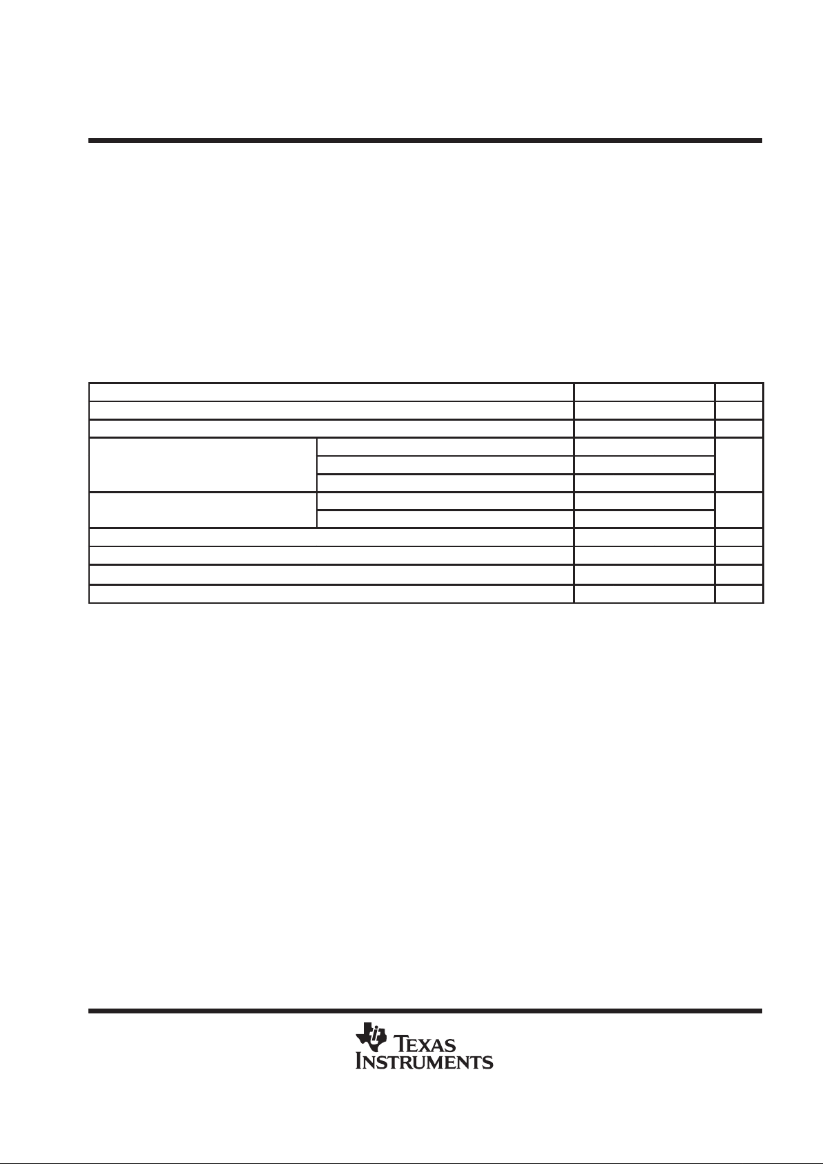
TMS320C5x, TMS320LC5x
DIGITAL SIGNAL PROCESSORS
SPRS030A – APRIL 1995 – REVISED APRIL 1996
45
POST OFFICE BOX 1443 • HOUSTON, TEXAS 77251–1443
absolute maximum ratings over operating ambient-air temperature range (unless otherwise noted)
(’320C5x only)
†
Supply voltage range, V
DD
(see Note 3) – 0.3 V to 7 V. . . . . . . . . . . . . . . . . . . . . . . . . . . . . . . . . . . . . . . . . . . . .
Input voltage range, VI – 0.3 V to 7 V. . . . . . . . . . . . . . . . . . . . . . . . . . . . . . . . . . . . . . . . . . . . . . . . . . . . . . . . . . . . .
Output voltage range, VO – 0.3 V to 7 V. . . . . . . . . . . . . . . . . . . . . . . . . . . . . . . . . . . . . . . . . . . . . . . . . . . . . . . . . .
Operating ambient temperature range, TA –40°C to 85°C. . . . . . . . . . . . . . . . . . . . . . . . . . . . . . . . . . . . . . . . . . .
Operating case temperature, TC 0°C to 85°C. . . . . . . . . . . . . . . . . . . . . . . . . . . . . . . . . . . . . . . . . . . . . . . . . . . . . .
Storage temperature range, T
stg
–55°C to 150°C. . . . . . . . . . . . . . . . . . . . . . . . . . . . . . . . . . . . . . . . . . . . . . . . . .
†
Stresses beyond those listed under “absolute maximum ratings” may cause permanent damage to the device. These are stress ratings only, and
functional operation of the device at these or any other conditions beyond those indicated under “recommended operating conditions” is not
implied. Exposure to absolute-maximum-rated conditions for extended periods may affect device reliability.
NOTE 3: All voltage values are with respect to VSS.
recommended operating conditions (’320C5x only)
MIN NOM MAX UNIT
V
DD
Supply voltage 4.75 5 5.25 V
V
SS
Supply voltage 0 V
X2/CLKIN, CLKIN2 3 VDD+0.3
V
IH
High-level input voltage
CLKX, CLKR, TCLKX, TCLKR
2.5 VDD+0.3
V
All other inputs 2 VDD+0.3
p
X2/CLKIN, CLKIN2, CLKX, CLKR, TCLKX, TCLKR – 0.3 0.7
VILLow-level input voltage
All other inputs – 0.3 0.8
V
I
OH
High-level output current (see Note 4) – 300
‡
µA
I
OL
Low-level output current 2 mA
T
C
Operating case temperature 0 85 °C
T
A
Operating ambient temperature –40 85 °C
‡
This IOH can be exceeded when using a 1-kΩ pulldown resistor on the TDM serial port TADD output; however, this output still meets V
OH
specifications under these conditions.
NOTE 4: Figure 9 shows the test load circuit and Figure 10 and Figure 11 show the voltage reference levels.
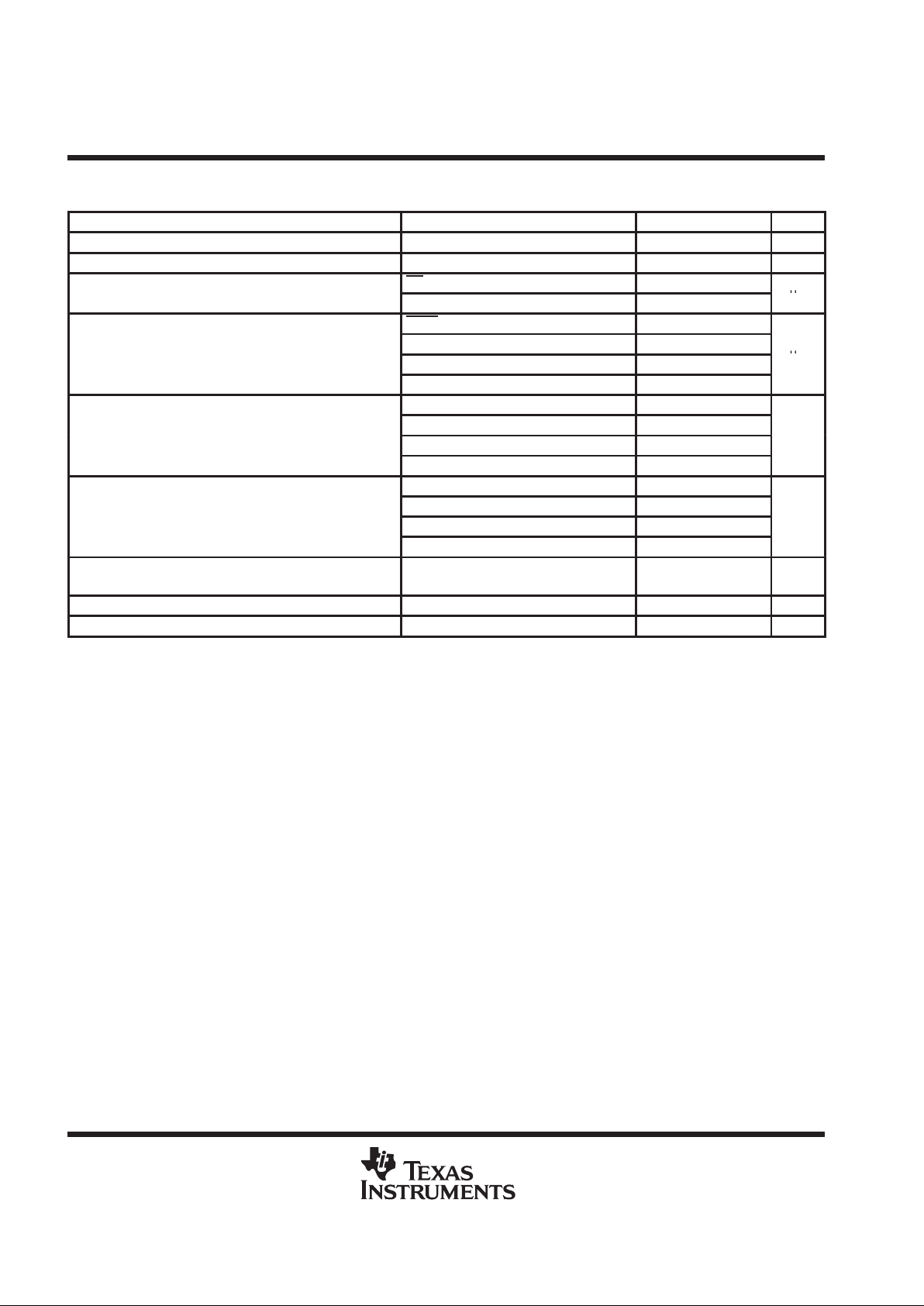
TMS320C5x, TMS320LC5x
DIGITAL SIGNAL PROCESSORS
SPRS030A – APRIL 1995 – REVISED APRIL 1996
46
POST OFFICE BOX 1443 • HOUSTON, TEXAS 77251–1443
electrical characteristics over recommended ranges of supply voltage and operating ambient-air
temperature (unless otherwise noted) (’320C5x only)
PARAMETER TEST CONDITIONS MIN TYP‡MAX UNIT
V
OH
High-level output voltage (see Note 4) IOH = 300 µA 2.4 3 V
V
OL
Low-level output voltage (see Note 4) IOL = 2 mA 0.3 0.6 V
p
p
BR (with internal pullup) – 500 20
IOZHigh-impedance output current (V
DD
= 5.25
V)
All other 3-state outputs –20 20
µ
A
TRST (with internal pulldown) –10 800
p
TMS, TCK, TDI (with internal pullups) – 500 10
IIInput current (V
I
=
V
SS
to VDD)
X2/CLKIN –50 50
µ
A
All other inputs –10 10
fx = 40 MHz, VDD = 5.25 V 60
pp
fx = 57 MHz, VDD = 5.25 V 67
I
DD(core)
Supply current, core CPU
fx = 80 MHz, VDD = 5.25 V 94
mA
fx = 100 MHz, VDD = 5.25 V 110
fx = 40 MHz, VDD = 5.25 V 40
pp
p
fx = 57 MHz, VDD = 5.25 V 45
I
DD(pins)
Supply current, pins
fx = 80 MHz, VDD = 5.25 V 63
mA
fx = 100 MHz, VDD = 5.25 V 75
I
DD(standby)
Supply current, standby
IDLE2, divide-by-two clock mode, clocks
shut off
5 µA
C
i
Input capacitance 15 pF
C
o
Output capacitance 15 pF
†
Typical values are at VDD = 5 V, TA = 25°C, unless otherwise specified.
NOTE 4: Figure 9 shows the test load circuit and Figure 10 and Figure 11 show the voltage reference levels.
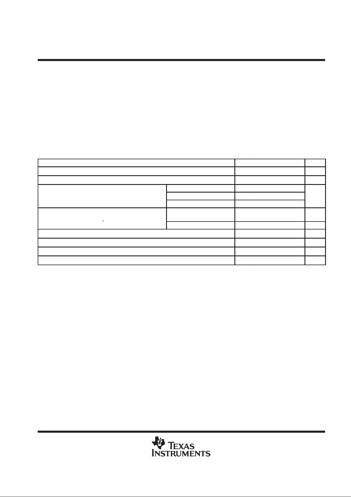
TMS320C5x, TMS320LC5x
DIGITAL SIGNAL PROCESSORS
SPRS030A – APRIL 1995 – REVISED APRIL 1996
47
POST OFFICE BOX 1443 • HOUSTON, TEXAS 77251–1443
absolute maximum ratings over specified temperature range (unless otherwise noted) (’320LC5x
only)
†
Supply voltage range, VDD (see Note 3) –0.3 V to 5 V. . . . . . . . . . . . . . . . . . . . . . . . . . . . . . . . . . . . . . . . . . . . . . .
Input voltage range, V
I
–0.3 V to 5 V. . . . . . . . . . . . . . . . . . . . . . . . . . . . . . . . . . . . . . . . . . . . . . . . . . . . . . . . . . . . . .
Output voltage range, V
O
–0.3 V to 5 V. . . . . . . . . . . . . . . . . . . . . . . . . . . . . . . . . . . . . . . . . . . . . . . . . . . . . . . . . . . .
Operating ambient temperature range, T
A
–40° to 85°C. . . . . . . . . . . . . . . . . . . . . . . . . . . . . . . . . . . . . . . . . . . . .
Operating case temperature, TC 0°C to 85°C. . . . . . . . . . . . . . . . . . . . . . . . . . . . . . . . . . . . . . . . . . . . . . . . . . . . . .
Storage temperature range, T
stg
–55° to 150°C. . . . . . . . . . . . . . . . . . . . . . . . . . . . . . . . . . . . . . . . . . . . . . . . . . . . .
†
Stresses beyond those listed under “absolute maximum ratings” may cause permanent damage to the device. These are stress ratings only, and
functional operation of the device at these or any other conditions beyond those indicated in the “recommended operating conditions” is not
implied. Exposure to absolute-maximum-rated conditions for extended periods may affect device reliability.
NOTE 3: All voltage values are with respect to VSS.
recommended operating conditions (’320LC5x only)
MIN NOM MAX UNIT
V
DD
Supply voltage
3.13 3.3 3.47 V
V
SS
Supply voltage
0 V
X2/CLKIN, CLKIN2 2.5 VDD+ 0.3
V
IH
High-level input voltage
CLKX, CLKR, TCLKX, TCLKR 2.0 VDD+ 0.3
V
All other inputs 1.8 VDD+ 0.3
V
Low-level input voltage
X2/CLKIN, CLKIN2, CLKX,
CLKR, TCLKX, TCLKR
–0.3 0.5 V
IL
o e e u o age
All other inputs –0.3 0.6 V
I
OH
High-level output current
– 300
‡
µA
I
OL
Low-level output current
2 mA
T
C
Operating case temperature
0 85 °C
T
A
Operating ambient temperature
–40 85 °C
‡
This IOH may be exceeded when using a 1-kΩ pulldown resistor on the TDM serial port TADD output; however, this output still meets V
OH
specifications under these conditions.
TMS320C5x, TMS320LC5x
DIGITAL SIGNAL PROCESSORS
SPRS030A – APRIL 1995 – REVISED APRIL 1996
48
POST OFFICE BOX 1443 • HOUSTON, TEXAS 77251–1443
electrical characteristics over recommended ranges of supply voltage and operating free-air
temperature (unless otherwise noted) (’320LC5x only)
PARAMETER TEST CONDITIONS MIN TYP
†
MAX UNIT
High-level output voltage
IOH = 300 µA 2.0
V
OH
gg
(see Note 4)
IOH = 20 µA
VDD– 0.3
‡
V
Low-level output voltage
IOL = 2 mA 0.4
V
OL
g
(see Note 4)
IOL = 20 µA
0.3
‡
V
High-impedance output current
BR (with internal pullup) –500 20
I
OZ
High im edance out ut current
(VDD = 3.47 V)
All other 3-state outputs
–20 20
µ
A
TRST(with internal pulldown) –10 800
TMS, TCK, TDI pins (with internal pullups) –500 10
I
I
Input current (VI = VSS to VDD)
X2/CLKIN (oscillator enabled)
–50
50
µA
I
(
ISS DD
)
X2/CLKIN (oscillator disabled)
–10
10
µ
All other inputs –10
10
fx = 40 MHz, VDD = 3.47 V 26
I
DD(core)
Supply current, core CPU
fx = 50 MHz, VDD = 3.47 V
33
mA
()
fx = 80 MHz, VDD = 3.47 V 53
fx = 40 MHz, VDD = 3.47 V 18
I
DD(pins)
Supply current, pins
fx = 50 MHz, VDD = 3.47 V
22
mA
()
fx = 80 MHz, VDD = 3.47 V 35
I
DD(standby)
Supply current, standby
IDLE2, divide-by-two clock mode, clocks
shut off
5 µA
C
i
Input capacitance 15 pF
C
o
Output capacitance 15 pF
†
All typical values are at VDD = 3.3 V, TA = 25°C.
‡
Values derived from characterization data and not tested
NOTE 4: Figure 9 shows the test load circuit and Figure 10 and Figure 11 show the voltage reference levels.

TMS320C5x, TMS320LC5x
DIGITAL SIGNAL PROCESSORS
SPRS030A – APRIL 1995 – REVISED APRIL 1996
49
POST OFFICE BOX 1443 • HOUSTON, TEXAS 77251–1443
PARAMETER MEASUREMENT INFORMATION
Tester Pin
Electronics
V
Load
I
OL
C
T
I
OH
Output
Under
Test
50 Ω
Where: I
OL
= 2 mA (all outputs) minimum
I
OH
= 300 µA (all outputs) minimum
V
LOAD
= 1.5 V
C
T
= 80-pF typical load circuit capacitance
Figure 9. Test Load Circuit
signal transition levels
The data in this section is shown for both the 5-V version (’C5x) and the 3.3-V version (’LC5x). In each case,
the 5-V data is shown followed by the 3.3-V data in parentheses. TTL-output levels are driven to a minimum
logic-high level of 2.4 V (2 V) and to a maximum logic-low level of 0.6 V (0.4 V). Figure 10 shows the TTL-level
outputs.
0.6 V (0.4 V)
1 V (0.8 V)
2 V (1.6 V)
2.4 V (2 V)
Figure 10. TTL-Level Outputs
TTL-output transition times are specified as follows:
D
For a
high-to-low transition
, the level at which the output is said to be no longer high is 2 V (1.6 V), and the
level at which the output is said to be low is 1 V (0.8 V).
D
For a
low-to-high transition
, the level at which the output is said to be no longer low is 1 V (0.8 V), and the
level at which the output is said to be high is 2 V (1.6 V).
Figure 11 shows the TTL-level inputs.
2 V (1.8 V)
0.8 V (0.6 V)
Figure 11. TTL-Level Inputs
TTL-compatible input transition times are specified as follows:
D
For a
high-to-low transition
on an input signal, the level at which the input is said to be no longer high is
2 V (1.8 V), and the level at which the input is said to be low is 0.8 V (0.6 V).
D
For a
low-to-high transition
on an input signal, the level at which the input is said to be no longer low is
0.8 V (0.6 V), and the level at which the input is said to be high is 2 V (1.8 V).

TMS320C5x, TMS320LC5x
DIGITAL SIGNAL PROCESSORS
SPRS030A – APRIL 1995 – REVISED APRIL 1996
50
POST OFFICE BOX 1443 • HOUSTON, TEXAS 77251–1443
PARAMETER MEASUREMENT INFORMATION
timing parameter symbology
Timing parameter symbols used are created in accordance with JEDEC Standard 100-A. To shorten the
symbols, some of the pin names and other related terminology have been abbreviated as follows:
Lowercase subscripts and their meanings: Letters and symbols and their meanings:
a access time H High
c cycle time (period) L Low
d delay time V Valid
dis disable time Z High impedance
en enable time
f fall time
h hold time
r rise time
su setup time
t transition time
v valid time
w pulse duration (width)
X Unknown, changing, or don’t care level

TMS320C5x, TMS320LC5x
DIGITAL SIGNAL PROCESSORS
SPRS030A – APRIL 1995 – REVISED APRIL 1996
51
POST OFFICE BOX 1443 • HOUSTON, TEXAS 77251–1443
CLOCK CHARACTERISTICS AND TIMING
The ’C5x can use either its internal oscillator or an external frequency source for a clock. The clock mode is
determined by the clock mode pins (CLKMD1, CLKMD2, and CLKMD3). Table 9 shows the standard clock
options available on the ’C50, ’LC50, ’C51, ’LC51, ’C52, ’LC52, ’C53, ’LC53, ’C53S, and ’LC53S. For these
devices, the CLKIN2 pin functions as the external frequency input when using the PLL options. An expanded
set of clock options is shown in Table 10 and is available on the ’LC56, ’C57S, and ’LC57 devices. For these
devices, X2/CLKIN functions as the external frequency input when using the PLL options.
Table 9. Standard Clock Options
CLKMD1 CLKMD2 CLOCK SOURCE
1 0 PLL clock generator option
†
0 1 Reserved for test purposes
1 1
External divide-by-two option or internal divide-by-two clock option
with an external crystal
0 0 External divide-by-two option with the internal oscillator disabled
†
PLL multiply-by-one option on ’C50, ’C51, ’C53, ’C53S devices, PLL multiply-by-two option on
’C52 device
Table 10. PLL Clock Option for ’LC56, ’C57S, and ’LC57
CLKMD1 CLKMD2 CLKMD3 CLOCK SOURCE
0 0 0 PLL multiply-by-three
0 1 0 PLL multiply-by-four
1 0 0 PLL multiply-by-five
1 1 0 PLL multiply-by-nine
0 0 1 External divide-by-two option with oscillator disabled
0 1 1 PLL multiply-by-two
1 0 1 PLL multiply-by-one
1 1 1 External/Internal divide-by-two with oscillator enabled

TMS320C5x, TMS320LC5x
DIGITAL SIGNAL PROCESSORS
SPRS030A – APRIL 1995 – REVISED APRIL 1996
52
POST OFFICE BOX 1443 • HOUSTON, TEXAS 77251–1443
internal divide-by-two clock option with external crystal
The internal oscillator is enabled by connecting a crystal across X1 and X2/CLKIN. The frequency of CLKOUT1
is one-half of the crystal’s oscillating frequency. The crystal should be in either fundamental or overtone
operation and parallel resonant, with an effective series resistance of 30 Ω and a power dissipation of 1 mW;
it should be specified at a load capacitance of 20 pF. Overtone crystals require an additional tuned-LC circuit.
Figure 12 shows an external crystal (fundamental frequency) connected to the on-chip oscillator.
recommended operating conditions for internal divide-by-two clock option
MIN NOM MAX UNIT
TMS320C5x-40 0
†
40.96
TMS320C5x-57 0
†
57.14
TMS320C5x-80 0
†
80
MH
z
f
clk
Input clock frequency
TMS320C5x-100
‡
0
†
100
TMS320LC5x-40 0
†
40
TMS320LC5x-50 0
†
50
MHz
TMS320LC5x-80 0
†
80
C1, C2 Load capacitance 10 pF
†
This device utilizes a fully static design and, therefore, can operate with input clock cycle time (t
c(CI)
) approaching ∞. The device is characterized
at frequencies approaching 0 Hz, but is tested at f
clk
= 6.7 MHz to meet device test time requirements.
‡
’320C51, ’320C52 currently available at this clock speed
X1 X2/CLKIN
C1 C2
Crystal
Figure 12. Internal Clock Option

TMS320C5x, TMS320LC5x
DIGITAL SIGNAL PROCESSORS
SPRS030A – APRIL 1995 – REVISED APRIL 1996
53
POST OFFICE BOX 1443 • HOUSTON, TEXAS 77251–1443
external divide-by-two clock option
An external frequency source can be used by injecting the frequency directly into X2/CLKIN with X1 left
unconnected. Refer to Table 9 and Table 10 for appropriate configuration of the CLKMD1, CLKMD2 and
CLKMD3 pins to generate the external divide-by-2 clock option. The external frequency injected must conform
to the specifications listed in the timing requirements table.
switching characteristics over recommended operating conditions [H = 0.5 t
c(CO)
] (’320C5x only)
(see Figure 13)
’320C5x-40 ’320C5x-57
PARAMETER
MIN TYP MAX MIN TYP MAX
UNIT
t
c(CO)
Cycle time, CLKOUT1 48.8 2t
c(CI)
†
35 2t
c(CI)
†
ns
t
d(CIH-COH/L)
Delay time, X2/CLKIN high to CLKOUT1 high/low 3 11 20 3 11 20 ns
t
f(CO)
Fall time, CLKOUT1 5 5 ns
t
r(CO)
Rise time, CLKOUT1 5 5 ns
t
w(COL)
Pulse duration, CLKOUT1 low H – 3 H H + 2 H – 3 H H + 2 ns
t
w(COH)
Pulse duration, CLKOUT1 high H – 3 H H + 2 H – 3 H H + 2 ns
’320C5x-80 ’320C5x-100
PARAMETER
MIN TYP MAX MIN TYP MAX
UNIT
t
c(CO)
Cycle time, CLKOUT1 25 2t
c(CI)
†
20 2t
c(CI)
†
ns
t
d(CIH-COH/L)
Delay time, X2/CLKIN high to CLKOUT1 high/low 1 9 18 1 9 18 ns
t
f(CO)
Fall time, CLKOUT1 4 4 ns
t
r(CO)
Rise time, CLKOUT1 4 4 ns
t
w(COL)
Pulse duration, CLKOUT1 low H – 3 H H + 2 H – 3 H H + 2 ns
t
w(COH)
Pulse duration, CLKOUT1 high H – 3 H H + 2 H – 3 H H + 2 ns
switching characteristics over recommended operating conditions [H = 0.5 t
c(CO)
] (’320LC5x only)
(see Figure 13)
’320LC5x-40 ’320LC5x-50 ’320LC5x-80 UNIT
PARAMETER
MIN TYP MAX MIN TYP MAX MIN TYP MAX UNIT
t
c(CO)
Cycle time, CLKOUT1 50 2t
c(CI)
†
40 2t
c(CI)
†
25 2t
c(CI)
†
ns
t
d(CIH-COH/L)
Delay time, X2/CLKIN high to
CLKOUT1 high/low
3 11 20 3 11 20 1 9 18 ns
t
f(CO)
Fall time, CLKOUT1 5 5 4 ns
t
r(CO)
Rise time, CLKOUT1 5 5 4 ns
t
w(COL)
Pulse duration, CLKOUT1 low H – 3 H H + 2 H – 3 H H + 2 H – 3 H H + 2 ns
t
w(COH)
Pulse duration, CLKOUT1 high H – 3 H H + 2 H – 3 H H + 2 H – 3 H H + 2 ns
†
This device utilizes a fully static design and, therefore, can operate with t
c(Cl)
approaching infinity. The device is characterized at frequencies
approaching 0 Hz but is tested at t
c(CO)
= 300 ns to meet device test time requirements.

TMS320C5x, TMS320LC5x
DIGITAL SIGNAL PROCESSORS
SPRS030A – APRIL 1995 – REVISED APRIL 1996
54
POST OFFICE BOX 1443 • HOUSTON, TEXAS 77251–1443
timing requirements over recommended ranges of supply voltage and operating ambient-air
temperature (’320C5x only) (see Figure 13)
’320C5x-40 ’320C5x-57 ’320C5x-80 ’320C5x-100
MIN MAX MIN MAX MIN MAX MIN MAX
UNIT
t
c(CI)
Cycle time, X2/CLKIN 24.4
†
17.5
†
12.5
†
10
†
ns
t
f(CI)
Fall time, X2/CLKIN
‡
5 5 4 4 ns
t
r(CI)
Rise time, X2/CLKIN
‡
5 5 4 4 ns
t
w(CIL)
Pulse duration, X2/CLKIN low 11
†
8
†
5
†
5
†
ns
t
w(CIH)
Pulse duration, X2/CLKIN high 11
†
8
†
5
†
5
†
ns
timing requirements over recommended ranges of supply voltage and operating ambient-air
temperature (’320LC5x only) (see Figure 13)
’320LC5x-40 ’320LC5x-50
’320LC5x-80
MIN MAX MIN MAX MIN MAX
UNIT
t
c(CI)
Cycle time, X2/CLKIN 25
†
20
†
12.5
†
ns
t
f(CI)
Fall time, X2/CLKIN
‡
5 5 4 ns
t
r(CI)
Rise time, X2/CLKIN
‡
5 5 4 ns
t
w(CIL)
Pulse duration, X2/CLKIN low 11
†
9
†
5
†
ns
t
w(CIH)
Pulse duration, X2/CLKIN high 11
†
9
†
5
†
ns
†
This device utilizes a fully static design and, therefore, can operate with t
c(Cl)
approaching ∞. The device is characterized at frequencies
approaching 0 Hz, but is tested at a minimum of t
c(Cl)
= 150 ns to meet device test time requirements.
‡
Values derived from characterization data and not tested
t
r(CO)
t
f(CO)
t
w(COH)
CLKOUT1
CLKIN
t
w(COL)
t
d(CIH-COH/L)
t
f(CI)
t
r(CI)
t
w(CIL)
t
w(CIH)
t
c(CO)
t
c(CI)
Figure 13. External Divide-by-Two Clock Timing

TMS320C5x, TMS320LC5x
DIGITAL SIGNAL PROCESSORS
SPRS030A – APRIL 1995 – REVISED APRIL 1996
55
POST OFFICE BOX 1443 • HOUSTON, TEXAS 77251–1443
PLL clock generator option
An external frequency source can be used by injecting the frequency directly into CLKIN2‡ with X1 left
unconnected and X2 connected to VDD. This external frequency is multiplied by the factors shown in Table 9
and T able 10 to generate the internal machine cycle. The multiply-by-one option is available on the ’C50, ’LC50,
’C51, ’LC51, ’C53, ’LC53, ’C53S and ’LC53S. The multiply-by-two option is available on the ’C52 and ’LC52.
Multiplication factors of 1, 2, 3, 4, 5, and 9 are available on the ’LC56, ’LC57, ’C57S and ’LC57S. Refer to T able 9
and T able 10 for appropriate configuration of the CLKMD1, CLKMD2 and CLKMD3 pins to generate the desired
PLL multiplication factor. The external frequency injected must conform to the specifications listed in the timing
requirements table.
switching characteristics over recommended operating conditions [H = 0.5 t
c(CO)
] (’320C5x only)
(see Figure 14)
’320C5x-40 ’320C5x-57
PARAMETER
MIN TYP MAX MIN TYP MAX
UNIT
t
c(CO)
Cycle time, CLKOUT1 48.8 75 35 75 ns
t
f(CO)
Fall time, CLKOUT1 5 5 ns
t
r(CO)
Rise time, CLKOUT1 5 5 ns
t
w(COL)
Pulse duration, CLKOUT1 low H – 3
†
H H + 2†H – 3
†
H H + 2
†
ns
t
w(COH)
Pulse duration, CLKOUT1 high H – 3
†
H H + 2†H – 3
†
H H + 2
†
ns
t
d(C2H-COH)
Delay time, CLKIN2 high to CLKOUT1
high
2 9 16 2 9 16 ns
t
d(TP)
Delay time, transitory phase—PLL
synchronized after CLKIN2 supplied
†
1000t
c(C2)
ĕ
1000t
c(C2)
ĕ
ns
’320C5x-80 ’320C5x-100
PARAMETER
MIN TYP MAX MIN TYP MAX
UNIT
t
c(CO)
Cycle time, CLKOUT1 25 55 20 45 ns
t
f(CO)
Fall time, CLKOUT1 4 4 ns
t
r(CO)
Rise time, CLKOUT1 4 4 ns
t
w(COL)
Pulse duration, CLKOUT1 low H – 3
†
H H + 2†H – 3
†
H H + 2
†
ns
t
w(COH)
Pulse duration, CLKOUT1 high H – 3
†
H H + 2†H – 3
†
H H + 2
†
ns
t
d(C2H-COH)
Delay time, CLKIN2 high to CLKOUT1
high
1 8 15 1 8 15 ns
t
d(TP)
Delay time, transitory phase—PLL
synchronized after CLKIN2 supplied
†
1000t
c(C2)
ĕ
1000t
c(C2)
ĕ
ns
†
Values assured by design and not tested
‡
On the TMS320C57S devices, CLKIN2 functions as the PLL clock input.

TMS320C5x, TMS320LC5x
DIGITAL SIGNAL PROCESSORS
SPRS030A – APRIL 1995 – REVISED APRIL 1996
56
POST OFFICE BOX 1443 • HOUSTON, TEXAS 77251–1443
switching characteristics over recommended operating conditions [H = 0.5 t
c(CO)
] (’320LC5x only)
(see Figure 14)
’320LC5x-40 ’320LC5x-50 ’320LC5x-80
PARAMETER
MIN TYP MAX MIN TYP MAX MIN TYP MAX
UNIT
t
c(CO)
Cycle time,
CLKOUT1
50 75
†
40 75
†
25 55
†
ns
t
d(C2H-COH)
Delay time,
CLKIN2 high to
CLKOUT1 high
2 9 16 2 9 16 1 8 15 ns
t
f(CO)
Fall time,
CLKOUT1
5 5 4 ns
t
r(CO)
Rise time,
CLKOUT1
5 5 4 ns
t
w(COL)
Pulse duration,
CLKOUT1 low
H–3
‡
H H+2‡H–3
‡
H H+2‡H–3
‡
H H+2‡ns
t
w(COH)
Pulse duration,
CLKOUT1 high
H–3
‡
H H+2‡H–3
‡
H H+2‡H–3
‡
H H+2‡ns
t
d(TP)
Delay time,
transitory
phase—PLL
synchronized
after CLKIN2
supplied
1000t
c(C2)
1000t
c(C2)
1000t
c(C2)
ns
†
Clocks can only be stopped while executing IDLE2 when using the PLL clock generator option.
‡
Values assured by design and not tested
§
On the ’LC56, ’LC57, and ’LC57S devices, CLKIN2 functions as the PLL clock input.

TMS320C5x, TMS320LC5x
DIGITAL SIGNAL PROCESSORS
SPRS030A – APRIL 1995 – REVISED APRIL 1996
57
POST OFFICE BOX 1443 • HOUSTON, TEXAS 77251–1443
timing requirements over recommended ranges of supply voltage and operating ambient-air
temperature (’320C5x only) (see Figure 14)
’320C5x-40 ’320C5x-57
MIN MAX MIN MAX
UNIT
Multiply-by-one
†
48.8 75
‡
35 75
‡
ns
t
c(C2)
Cycle time, CLKIN2
Multiply-by-two
§
97.6 150
‡
70 150
‡
ns
t
f(C2)
Fall time, CLKIN2
¶
5 5 ns
t
r(C2)
Rise time, CLKIN2
¶
5 5 ns
t
w(C2L)
Pulse duration, CLKIN2 low 15 t
c(C2)
–15 11 t
c(C2)
–11 ns
t
w(C2H)
Pulse duration, CLKIN2 high 15 t
c(C2)
–15 11 t
c(C2)
–11 ns
’320C5x-80 ’320C5x-100
MIN MAX MIN MAX
UNIT
Multiply-by-one
†
25 75
‡
20 75
‡
ns
t
c(C2)
Cycle time, CLKIN2
Multiply-by-two
§
50 150
‡
40 110
‡
ns
t
f(C2)
Fall time, CLKIN2
¶
4 4 ns
t
r(C2)
Rise time, CLKIN2
¶
4 4 ns
t
w(C2L)
Pulse duration, CLKIN2 low 8 t
c(C2)
–8 7 t
c(C2)
–7 ns
t
w(C2H)
Pulse duration, CLKIN2 high 8 t
c(C2)
–8 7 t
c(C2)
–7 ns
timing requirements over recommended ranges of supply voltage and operating ambient-air
temperature (’320LC5x only) (see Figure 14)
’320LC5x-40 ’320LC5x-50 ’320LC5x-80
MIN MAX MIN MAX MIN MAX
UNIT
Multiply-by-one
†
50 75
‡
40 75
‡
25 37.5
‡
ns
t
c(C2)
Cycle time, CLKIN2
Multiply-by-two
§
100 150
‡
80 150
‡
50 110
‡
ns
t
f(C2)
Fall time, CLKIN2
¶
5 5 4 ns
t
r(C2)
Rise time, CLKIN2
¶
5 5 4 ns
t
w(C2L)
Pulse duration, CLKIN2 low 15 t
c(C2)
–15 13 t
c(C2)
–13 8 t
c(C2)
–8 ns
t
w(C2H)
Pulse duration, CLKIN2 high 15 t
c(C2)
–15 13 t
c(C2)
–13 8 t
c(C2)
–8 ns
†
Not available on ’C52, ’LC52
‡
Clocks can be stopped only while executing IDLE2 when using the PLL clock generator option. The t
d(TP)
(the transitory phase) occurs when
restarting clock from IDLE2 in this mode.
§
Available on ’C52, ’LC52, ’LC56, ’C57S, ’LC57, and ’LC57S
¶
Values derived from characterization data and not tested
t
r(C2)
t
w(C2L)
t
w(C2H)
t
d(TP)
t
c(CO)
t
c(C2)
t
w(COH)
t
f(CO)
t
r(CO)
t
f(C2)
CLKIN2
CLKOUT1
t
d(C2H-COH)
t
w(COL)
Unstable
Figure 14. PLL Clock Generator Timing

TMS320C5x, TMS320LC5x
DIGITAL SIGNAL PROCESSORS
SPRS030A – APRIL 1995 – REVISED APRIL 1996
58
POST OFFICE BOX 1443 • HOUSTON, TEXAS 77251–1443
MEMORY AND PARALLEL I/O INTERFACE READ
switching characteristics over recommended operating conditions [H = 0.5t
c(CO)
] (’320C5x only)
(see Figure 15)
’320C5x-40 ’320C5x-57 ’320C5x-80 ’320C5x-100
PARAMETER
MIN MAX MIN MAX MIN MAX MIN MAX
UNIT
t
su(AV-RDL)
Setup time, address valid before
RD
low
†
H – 10
‡
H – 10
‡
H – 7
‡
H – 6
‡
ns
t
h(RDH-AV)
Hold time, address valid after RD
high
†
0
‡
0
‡
0
‡
0
‡
ns
t
w(RDL)
Pulse duration, RD low
§¶#
H – 2 H + 2 H – 2 H + 2 H – 2 H + 2 H – 2 H + 2 ns
t
w(RDH)
Pulse duration, RD high
§¶#
H – 2 H – 2 H – 2 H – 2 ns
t
d(CO-ST)
Delay time, CLKOUT1 to STRB
rising or falling edge
§¶
– 1 3 – 2 2 – 2 2 – 2 2 ns
t
d(CO-RD)
Delay time, CLKOUT1 to RD rising
or falling edge
§¶
– 3 1 – 3 1 – 3 1 – 3 1 ns
t
d(RDH-WEL)
Delay time, RD high to WE low 2H – 5 2H – 5 2H – 4 2H – 4 ns
switching characteristics over recommended operating conditions [H = 0.5t
c(CO)
] (’320LC5x only)
(see Figure 15)
PARAMETER
’320LC5x-40
’320LC5x-50
’320LC5x-80
UNIT
MIN MAX MIN MAX
t
su(AV-RDL)
Setup time, address valid before RD low
†
H–10
‡
H – 7
‡
ns
t
h(RDH-AV)
Hold time, address valid after RD high
†
0
‡
0
‡
ns
t
w(RDL)
Pulse duration, RD low
§¶#
H–2 H+2 H–2 H+2 ns
t
w(RDH)
Pulse duration, RD high
§¶#
H–2 H–2 ns
t
d(RDH-WEL)
Delay time, RD high to WE low 2H – 5 2H – 4 ns
t
d(CO-RD)
Delay time, CLKOUT1 to RD rising or falling edge
§¶
–2 2 –3 1 ns
t
d(CO-ST)
Delay time, CLKOUT1 to STRB rising or falling edge
§¶
0 4 –2 2 ns
†
A0–A15, PS, DS, IS, R/W, and BR timings all are included in timings referenced as address.
‡
See Figure 16 for address bus timing variation with load capacitance.
§
These timings are for the cycles following the first cycle after reset, which is always seven wait states.
¶
Values are derived from characterization data and not tested.
#
Timings are valid for zero wait-state cycles only.
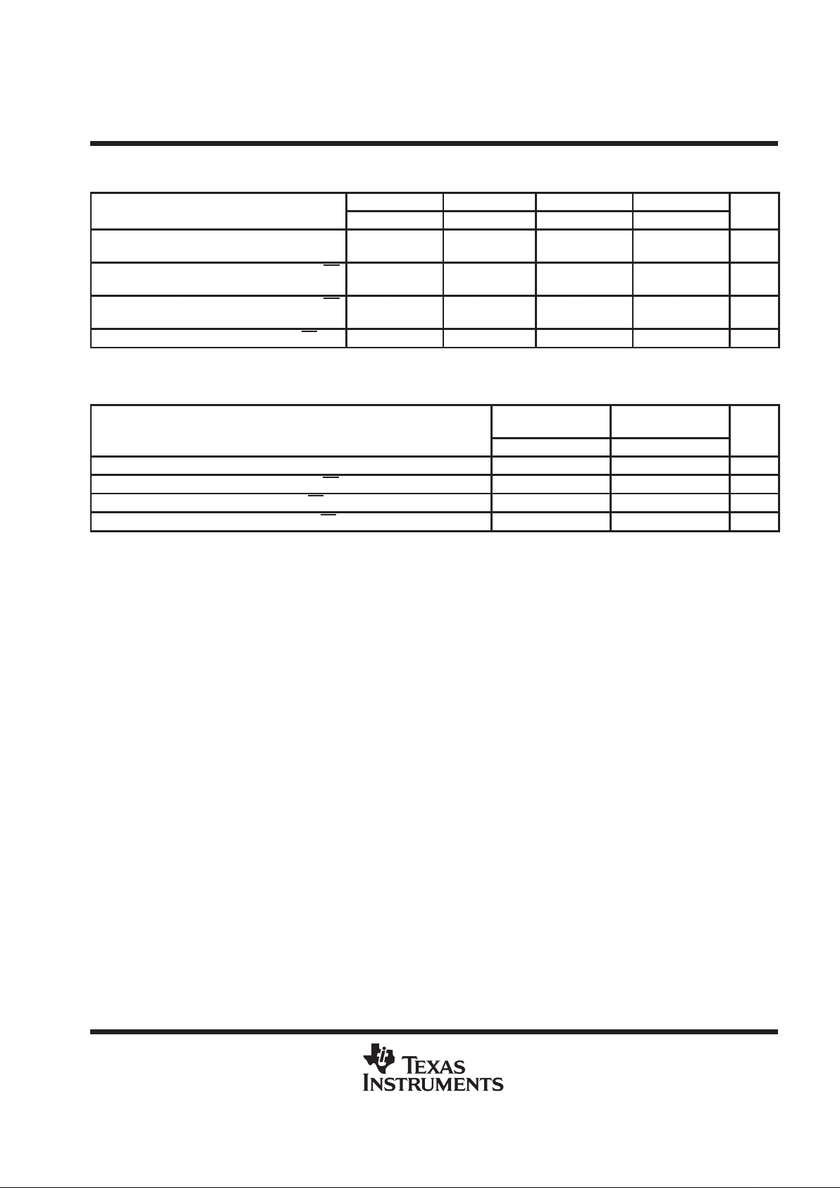
TMS320C5x, TMS320LC5x
DIGITAL SIGNAL PROCESSORS
SPRS030A – APRIL 1995 – REVISED APRIL 1996
59
POST OFFICE BOX 1443 • HOUSTON, TEXAS 77251–1443
timing requirements over recommended ranges of supply voltage and operating ambient-air
temperature [H = 0.5t
c(CO)
] (’320C5x only) (see Figure 15)
’320C5x-40 ’320C5x-57 ’320C5x-80 ’320C5x-100
MIN MAX MIN MAX MIN MAX MIN MAX
UNIT
t
a(RDAV)
Access time, read data from
address valid
2H – 18
†
2H – 15
†
2H – 10
†
2H – 10
†
ns
t
a(RDL-RD)
Access time, read data after RD
low
H – 10 H – 10 H – 7 H – 6 ns
t
su(RD-RDH)
Setup time, read data before RD
high
10 10 7 6 ns
t
h(RDH-RD)
Hold time, read data after RD high 0 0 0 0 ns
timing requirements over recommended ranges of supply voltage and operating ambient-air
temperature [H = 0.5t
c(CO)
] (’320LC5x only) (see Figure 15)
’320LC5x-40
’320LC5x-50
’320LC5x-80
UNIT
MIN MAX MIN MAX
t
a(RDAV)
Access time, read data from address valid 2H– 17
†
2H – 10
†
ns
t
su(RD-RDH)
Setup time, read data before RD high 10 7 ns
t
h(RDH-RD)
Hold time, read data after RD high 0 0 ns
t
a(RDL-RD)
Access time, read data after RD low H–10 H–7 ns
†
See Figure 16 for address bus timing variation with load capacitance.
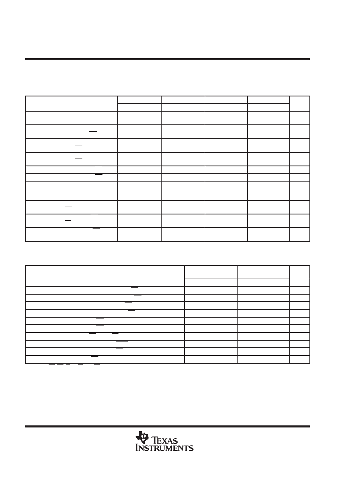
TMS320C5x, TMS320LC5x
DIGITAL SIGNAL PROCESSORS
SPRS030A – APRIL 1995 – REVISED APRIL 1996
60
POST OFFICE BOX 1443 • HOUSTON, TEXAS 77251–1443
MEMORY AND PARALLEL I/O INTERFACE WRITE
switching characteristics over recommended operating conditions [H = 0.5t
c(CO)
] (’320C5x only)
(see Figure 15)
’320C5x-40 ’320C5x-57 ’320C5x-80 ’320C5x-100
PARAMETER
MIN MAX MIN MAX MIN MAX MIN MAX
UNIT
t
su(AV-WEL)
Setup time, address valid
before WE
low
†
H–5
‡
H–5
‡
H–4
‡
H–3
‡
ns
t
su(WDV-WEH)
Setup time, write data
valid before WE
high
2H – 20 2H
§¶
2H – 20 2H§¶2H – 14 2H§¶2H – 14 2H
§¶
ns
t
h(WEH-AV)
Hold time, address valid
after WE
high
†
H–10
‡
H–10
‡
H–7
‡
H–7
‡
ns
t
h(WEH-WDV)
Hold time, write data valid
after WE
high
H–5 H+10
§
H–5 H+10
§
H–4 H+7
§
H–4 H+7§ns
t
w(WEL)
Pulse duration, WE low
§¶
2H – 2 2H + 2§2H – 2 2H + 2§2H – 2 2H + 2 2H – 2 2H + 2 ns
t
w(WEH)
Pulse duration, WE high§2H – 2 2H – 2 2H – 2 2H – 2 ns
t
d(CO-ST)
Delay time, CLKOUT1 to
STRB
rising or falling
edge
§
–1 3 –2 2 –2 2 –2 2 ns
t
d(CO-WE)
Delay time, CLKOUT1 to
WE
rising or falling edge
§
0 4 –1 3 –1 3 –1 3 ns
t
d(WEH-RDL)
Delay time, WE high to
RD
low
3H – 10 3H – 10 3H – 7 3H – 7 ns
t
en(WEL-BUd)
Enable time, WE low to
data bus driven
–5
§
–5
§
–4
§
–4
§
ns
switching characteristics over recommended operating conditions [H = 0.5t
c(CO)
] (’320LC5x only)
(see Figure 15)
PARAMETER
’320LC5x-40
’320LC5x-50
’320LC5x-80
UNIT
MIN MAX MIN MAX
t
su(AV-WEL)
Setup time, address valid before WE low
†
H–7
‡
H–4
‡
ns
t
su(WDV-WEH)
Setup time, write data valid before WE high
#
2H – 20 2H
§¶
2H – 14 2H
§¶
ns
t
h(WEH-AV)
Hold time, address valid after WE high
†
H–10
‡
H–7
‡
ns
t
h(WEH-WDV)
Hold time, write data valid after WE high H–5 H+10
§
H–4 H+7§ns
t
w(WEL)
Pulse duration, WE low
¶§
2H – 4 2H + 2 2H – 4 2H + 2 ns
t
w(WEH)
Pulse duration, WE high
¶
2H – 2 2H – 2 ns
t
d(WEH-RDL)
Delay time, WE high to RD low 3H – 10 3H – 7 ns
t
d(CO-ST)
Delay time, CLKOUT1 to STRB rising or falling edge
¶
0 4 –2 2 ns
t
d(CO-WE)
Delay time, CLKOUT1 to WE rising or falling edge
¶
0 4 –1 3 ns
t
en(WE-BUd)
Enable time, WE to data bus driven –5
§
–4
§
ns
†
A0–A15, PS
, DS, IS, R/W, and BR timings are all included in timings referenced as address.
‡
See Figure 16 for address bus timing variation with load capacitance.
§
Values derived from characterization data and not tested
¶
This value holds true for zero wait states or one software wait state only.
#
STRB
and WE edges are 0–4 ns from CLKOUT1 edges on writes. Rising and falling edges of these signals track each other; tolerance of resulting
pulsewidths is ±2 ns, not ±4 ns.
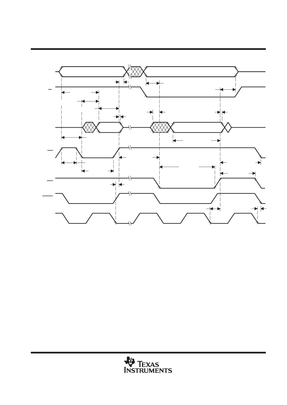
TMS320C5x, TMS320LC5x
DIGITAL SIGNAL PROCESSORS
SPRS030A – APRIL 1995 – REVISED APRIL 1996
61
POST OFFICE BOX 1443 • HOUSTON, TEXAS 77251–1443
MEMORY AND PARALLEL I/O INTERFACE WRITE (CONTINUED)
t
h(RDH-AV)
t
su(AV-WEL)
t
h(WEH-AV)
t
h(WEH-WDV)
t
en(WEL-BUd)
t
h(RDH-RD)
t
a(RDAV)
t
su(AV-RDL)
t
w(RDH)
t
w(RDL)
t
d(RDH-WEL)
t
w(WEL)
t
d(WEH-RDL)
t
w(WEH)
t
su(WDV-WEH)
t
d(CO-RD)
t
d(CO-WE)
t
d(CO-ST)
WE
RD
DATA
R/W
A0–A15
STRB
CLKOUT1
VALID
VALID VALID
VALID
t
a(RDL-RD)
t
su(RD-RDH)
NOTES: A. All timings are for 0 wait states. However , external writes always require two cycles to prevent external bus conflicts. The diagram
illustrates a one-cycle read and a two-cycle write and is not drawn to scale. All external writes immediately preceded by an external
read or immediately followed by an external read require three machine cycles.
B. Refer to Appendix B of
TMS320C5x User’s Guide
(literature number SPRU056) for logical timings of external interface.
Figure 15. Memory and Parallel I/O Interface Read and Write Timing

TMS320C5x, TMS320LC5x
DIGITAL SIGNAL PROCESSORS
SPRS030A – APRIL 1995 – REVISED APRIL 1996
62
POST OFFICE BOX 1443 • HOUSTON, TEXAS 77251–1443
MEMORY AND PARALLEL I/O INTERFACE WRITE (CONTINUED)
2.00
1.00
0.75
0.50
0.25
1.25
1.50
1.75
10 30 55 70 8515 20 25 4535 40 50 8060 65 75 90 95 100
Change in Address Bus Timing– ns
Change in Load Capacitance – pF
Figure 16. Address Bus Timing Variation With Load Capacitance

TMS320C5x, TMS320LC5x
DIGITAL SIGNAL PROCESSORS
SPRS030A – APRIL 1995 – REVISED APRIL 1996
63
POST OFFICE BOX 1443 • HOUSTON, TEXAS 77251–1443
READY TIMING FOR EXTERNALLY-GENERATED WAIT STATES
timing requirements over recommended ranges of supply voltage and operating ambient-air
temperature (see Note 5) (see Figure 17 and Figure 18)
’320C5x-40
’320C5x-57
’320LC5x-40
’320LC5x-50
’320C5x-80
’320LC5x-80
’320C5x-100
UNIT
MIN MAX MIN MAX MIN MAX
t
su(RY-COH)
Setup time, READY before CLKOUT1 rising edge 10 7 6 ns
t
su(RY-RDL)
Setup time, READY before RD falling edge 10 7 6 ns
t
h(COH-RYH)
Hold time, READY after CLKOUT1 rising edge 0 0 0 ns
t
h(RDL-RY)
Hold time, READY after RD falling edge 0 0 0 ns
t
h(WEL-RY)
Hold time, READY after WE falling edge H + 5 H + 4 H + 3 ns
t
v(WEL-RY)
Valid time, READY after WE falling edge H – 15 H – 10 H – 8 ns
NOTE 5: The external READY input is sampled only after the internal software wait states are completed.
READY
A0–A15
CLKOUT1
RD
Wait State
Generated
by READY
Wait State
Generated
Internally
t
h(RDL-RY)
t
su(RY-COH)
t
su(RY-COH)
t
h(COH-RYH)
t
su(RY-RDL)
Figure 17. Ready Timing for Externally-Generated Wait States During an External Read Cycle
READY
A0–A15
CLKOUT1
Wait State Generated by READY
WE
t
h(COH-RYH)
t
su(RY-COH)
t
h(WEL-RY)
t
v(WEL-RY)
Figure 18. Ready Timing for Externally-Generated Wait States During an External Write Cycle
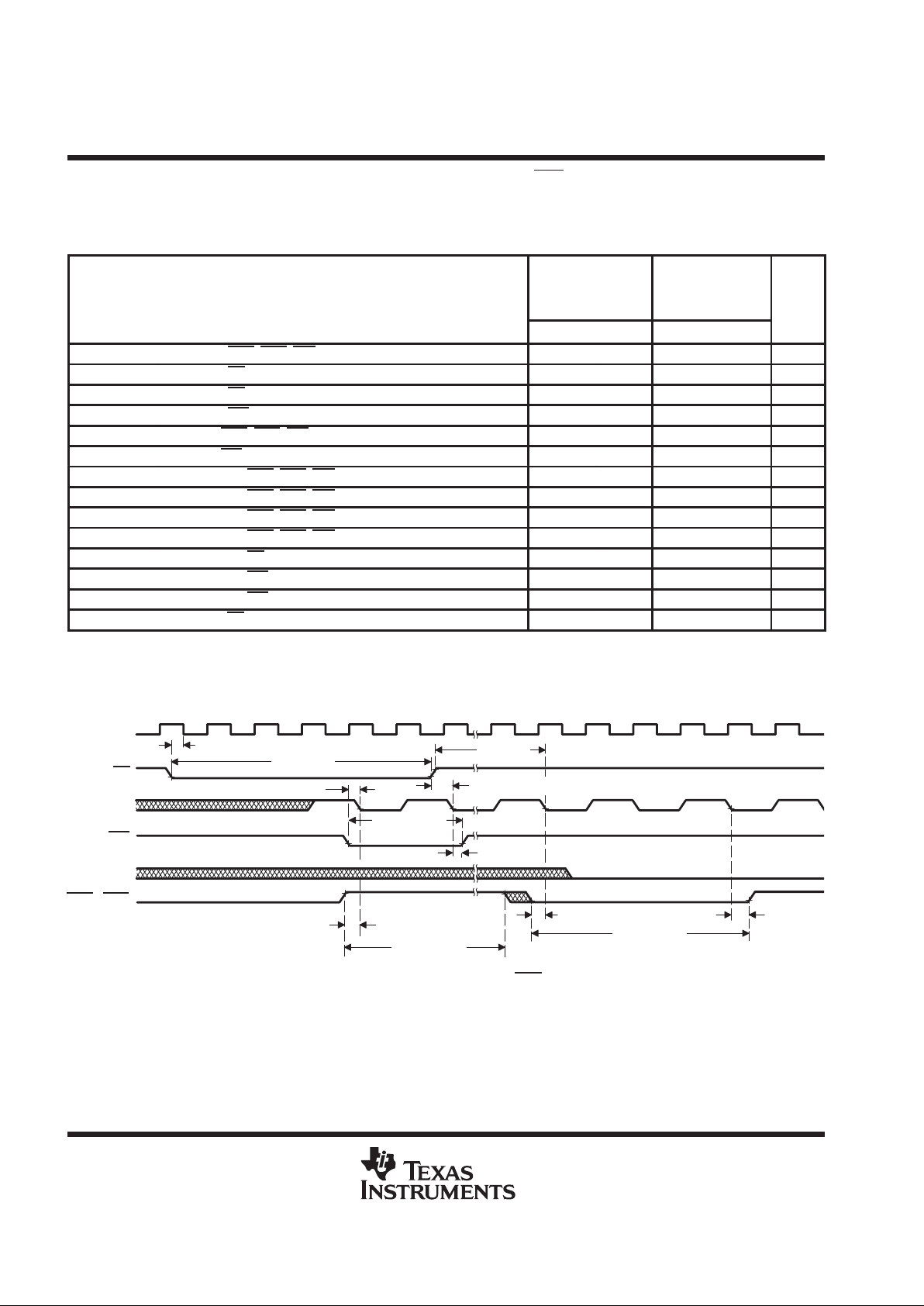
TMS320C5x, TMS320LC5x
DIGITAL SIGNAL PROCESSORS
SPRS030A – APRIL 1995 – REVISED APRIL 1996
64
POST OFFICE BOX 1443 • HOUSTON, TEXAS 77251–1443
RESET, INTERRUPT, AND BIO
timing requirements over recommended ranges of supply voltage and operating ambient-air
temperature [H = 0.5t
c(CO)
] (see Figure 19)
’320C5x-40
’320C5x-57
’320LC5x-40
’320LC5x-50
’320C5x-80
’320C5x-100
’320LC5x-80
UNIT
MIN MAX MIN MAX
t
su(IN-COL)
Setup time, INT1–INT4, NMI before CLKOUT1 low
†
15 10 ns
t
su(RS-COL)
Setup time, RS before CLKOUT1 low 15 2H – 5
‡
10 2H – 5
‡
ns
t
su(RS-CIL)
Setup time, RS before X2/CLKIN low 10 7 ns
t
su(BI-COL)
Setup time, BIO before CLKOUT1 low 15 10 ns
t
h(COL-IN)
Hold time, INT1–INT4, NMI after CLKOUT1 low
†
0 0 ns
t
h(COL-BI)
Hold time, BIO after CLKOUT1 low 0 0 ns
t
w(INL)SYN
Pulse duration, INT1–INT4, NMI low, synchronous 4H + 15
§
4H + 10
§
ns
t
w(INH)SYN
Pulse duration, INT1–INT4, NMI high, synchronous 2H + 15
§
2H + 10
§
ns
t
w(INL)ASY
Pulse duration, INT1–INT4, NMI low, asynchronous
‡
6H + 15
§
6H + 10
§
ns
t
w(INH)ASY
Pulse duration, INT1–INT4, NMI high, asynchronous
‡
4H + 15
§
4H + 10
§
ns
t
w(RSL)
Pulse duration, RS low 12H 12H ns
t
w(BIL)SYN
Pulse duration, BIO low, synchronous 15 10 ns
t
w(BIL)ASY
Pulse duration, BIO low, asynchronous
‡
H+15 H+10 ns
t
d(RSH)
Delay time, RS high to reset vector fetch 34H 34H ns
†
These parameters must be met to use the synchronous timings. Both reset and the interrupts can operate asynchronously. The pulse durations
require an extra half-cycle to ensure internal synchronization.
‡
Values derived from characterization data and not tested
§
If in IDLE2, add 4H to these timings.
BIO
RS
X2/CLKIN
t
su(RS-CIL)
t
su(BI-COL)
t
su(IN-COL)
t
h(COL-BI)
A0–A15
t
su(IN-COL)
t
h(COL-IN)
t
w(BIL)SYN
t
d(RSH)
CLKOUT1
t
w(RSL)
INT4
–INT1
t
w(INH)SYN
t
w(INL)SYN
t
su(RS-COL)
Figure 19. Reset, Interrupt, and BIO Timings

TMS320C5x, TMS320LC5x
DIGITAL SIGNAL PROCESSORS
SPRS030A – APRIL 1995 – REVISED APRIL 1996
65
POST OFFICE BOX 1443 • HOUSTON, TEXAS 77251–1443
INSTRUCTION ACQUISITION (IAQ), INTERRUPT ACKNOWLEDGE (IACK),
EXTERNAL FLAG (XF), AND TOUT (SEE NOTE 6)
switching characteristics over recommended operating conditions [H = 0.5t
c(CO)
] (see Figure 20)
PARAMETER
’320C5x-40
’320C5x-57
’320LC5x-40
’320LC5x-50
’320C5x-80
’320C5x-100
’320LC5x-80
UNIT
MIN MAX MIN MAX
t
su(AV-IQL)
Setup time, address valid before IAQ low
†
H–12
‡
H–9
‡
ns
t
h(IQL-AV)
Hold time, address valid after IAQ low H–10
‡
H–7
‡
ns
t
w(IQL)
Pulse duration, IAQ low H–10
‡
H–7
‡
ns
t
d(CO-TU)
Delay time, CLKOUT1 falling edge to TOUT –6 6 –6 6 ns
t
su(AV-IKL)
Setup time, address valid before IACK low
§
H–12
‡
H–9
‡
ns
t
h(IKL-AV)
Hold time, address valid after IACK low H–10
‡
H–7
‡
ns
t
w(IKL)
Pulse duration, IACK low H–10
‡
H–7
‡
ns
t
w(TUH)
Pulse duration, TOUT high 2H – 12 2H – 9 ns
t
d(CO-XFV)
Delay time, XF valid after CLKOUT1 0 12 0 9 ns
†
IAQ goes low during an instruction acquisition. It goes low only on the first cycle of the read when wait states are used. The falling edge should
be used to latch the valid address. The AVIS bit in the PMST register must be set to zero for the address to be valid when the instruction being
addressed resides in on-chip memory.
‡
Valid only if the external address reflects the current instruction activity (that is, code is executing on chip with no external bus cycles and AVIS
is on or code is executing off chip)
§
IACK
goes low during the fetch of the first word of the interrupt vector. It goes low only on the first cycle of the read when wait states are used.
Address pins A1–A4 can be decoded at the falling edge to identify the interrupt being acknowledged. The AVIS bit in the PMST register must
be set to zero for the address to be valid when the vectors reside in on-chip memory.
NOTE 6: IAQ
pin is not present on 100-pin packages.
IACK
pin is not present on 100-pin and 128-pin packages.

TMS320C5x, TMS320LC5x
DIGITAL SIGNAL PROCESSORS
SPRS030A – APRIL 1995 – REVISED APRIL 1996
66
POST OFFICE BOX 1443 • HOUSTON, TEXAS 77251–1443
INSTRUCTION ACQUISITION (IAQ), INTERRUPT ACKNOWLEDGE (IACK),
EXTERNAL FLAG (XF), AND TOUT (SEE NOTE 6) (CONTINUED)
CLKOUT1
STRB
IACK
†
IAQ
†
ADDRESS
t
d(CO-TU)
t
w(IKL)
t
su(AV-IKL)
t
su(AV-IQL)
t
w(IQL)
t
h(IKL-AV)
t
h(IQL-AV)
XF
TOUT
t
d(CO-XFV)
t
w(TUH)
t
d(CO-TU)
†
IAQ
and IACK are not affected by wait states.
Figure 20. IAQ, IACK, and XF Timings Example With Two External Wait States

TMS320C5x, TMS320LC5x
DIGITAL SIGNAL PROCESSORS
SPRS030A – APRIL 1995 – REVISED APRIL 1996
67
POST OFFICE BOX 1443 • HOUSTON, TEXAS 77251–1443
EXTERNAL DMA
switching characteristics over recommended operating conditions [H = 0.5t
c(CO)
] (see Note 7)
(see Figure 21)
PARAMETER
’320C5x-40
’320C5x-57
’320LC5x-40
’320LC5x-50
’320C5x-80
’320LC5x-80
’320C5x-100
UNIT
MIN MAX MIN MAX MIN MAX
t
d(HOL-HAL)
Delay time, HOLD low to HOLDA low 4H
†
4H
†
4H
†
ns
t
d(HOH-HAH)
Delay time, HOLD high before HOLDA high 2H 2H 2H ns
t
h(AZ-HAL)
Address high-impedance before HOLDA low
‡
H–15
§
H–10
§
H–8
§
ns
t
en(HAH-Ad)
Enable time, HOLDA high to address driven H–5
§
H–4
§
H–3
§
ns
t
d(XBL-IQL)
Delay time, XBR low to IAQ low 4H
§
6H
§
4H§6H
§
4H§6H
§
ns
t
d(XBH-IQH)
Delay time, XBR high to IAQ high 2H
§
4H
§
2H§4H
§
2H§4H
§
ns
t
d(XSL-RDV)
Delay time, read data valid after XSTRB low 40 29 25 ns
t
h(XSH-RD)
Hold time, read data valid after XSTRB high 0 0 0 ns
t
en(IQL-RDd)
Enable time, IAQ low to read data driven
¶
0§2H
§
0§2H
§
0§2H
§
ns
t
h(XRL-DZ)
Hold time, XR/W low to data high impedance 0
§
15
§
0
§
10
§
0
§
8 ns
t
h(IQH-DZ)
Hold time, IAQ high to data high impedance H
§
H
§
H
§
ns
t
en(D-XRH)
Enable time, data from XR/W going high 4
§
3
§
2
§
ns
†
HOLD is not acknowledged until current external access request is complete.
‡
This parameter includes all memory control lines.
§
Values derived from characterization data and not tested
¶
This parameter refers to the delay between the time the condition (IAQ
= 0 and XR/W = 1) is satisfied and the time that the ’C5x data lines become
valid.
NOTE 7: X preceding a name refers to external drive of the signal.
timing requirements over recommended ranges of supply voltage and operating ambient-air
temperature (see Note 7) (see Figure 21)
’320C5x-40
’320C5x-57
’320LC5x-40
’320LC5x-50
’320C5x-80
’320LC5x-80
’320C5x-100
UNIT
MIN MAX MIN MAX MIN MAX
t
d(HAL-XBL)
Delay time, HOLDA low to XBR low
#
0
§
0
§
0
§
ns
t
d(IQL-XSL)
Delay time, IAQ low to XSTRB low
#
0
§
0
§
0
§
ns
t
su(AV-XSL)
Setup time, Xaddress valid before XSTRB low 15 12 10 ns
t
su(DV-XSL)
Setup time, Xdata valid before XSTRB low 15 12 10 ns
t
h(XSL-D)
Hold time, Xdata hold after XSTRB low 15 12 10 ns
t
h(XSL-WA)
Hold time, write Xaddress hold after XSTRB low 15 12 10 ns
t
w(XSL)
Pulse duration, XSTRB low 45 40 35 ns
t
w(XSH)
Pulse duration, XSTRB high 45 40 35 ns
t
su(RW-XSL)
Setup time, R/W valid before XSTRB low 20 20 18 ns
t
h(XSH-RA)
Hold time, read Xaddress after XSTRB high 0 0 0 ns
§
Values derived from characterization data and not tested
#
XBR
, XR/W, and XSTRB lines must be pulled up with a 10-kΩ resistor to be certain that they are in an inactive high state during the transition
period between the ’C5x driving them and the external circuit driving them.
NOTE 7: X preceding a name refers to external drive of the signal.

TMS320C5x, TMS320LC5x
DIGITAL SIGNAL PROCESSORS
SPRS030A – APRIL 1995 – REVISED APRIL 1996
68
POST OFFICE BOX 1443 • HOUSTON, TEXAS 77251–1443
EXTERNAL DMA (CONTINUED)
XDATA(WR)
DATA(RD)
XADDRESS
XR/W
XSTRB
IAQ
XBR
ADDRESS
BUS/
CONTROL
SIGNALS
HOLDA
HOLD
t
su(DV-XSL)
t
h(XRL-DZ)
t
d(IQL-XSL)
t
d(XBL-IQL)
t
d(HAL-XBL)
t
en(HAH-Ad)
t
h(AZ-HAL)
t
d(HOH-HAH)
t
d(HOL-HAL)
t
su(AV-XSL)
t
w(XSH)
t
su(RW-XSL)
t
w(XSL)
t
d(XBH-IQH)
t
en(IQL-RDd)
t
en(D-XRH)
t
h(IQH-DZ)
t
en(IQL-RDd)
t
su(AV-XSL)
t
h(XSL-WA)
t
h(XSL-D)
t
h(XSH-RA)
t
d(XSL-RDV)
t
h(XSH-RD)
Figure 21. External DMA Timing

TMS320C5x, TMS320LC5x
DIGITAL SIGNAL PROCESSORS
SPRS030A – APRIL 1995 – REVISED APRIL 1996
69
POST OFFICE BOX 1443 • HOUSTON, TEXAS 77251–1443
SERIAL-PORT RECEIVE TIMING
timing requirements over recommended ranges of supply voltage and operating ambient-air
temperature [H = 0.5t
c(CO)
] (see Figure 22)
’320C5x-40
’320C5x-57
’320LC5x-40
’320LC5x-50
’320C5x-80
’320LC5x-80
’320C5x-100
UNIT
MIN MAX MIN MAX MIN MAX
t
c(SCK)
Cycle time, serial-port clock 5.2H
† ‡
5.2H
† ‡
5.2H
† ‡
ns
t
f(SCK)
Fall time, serial-port clock 8
§
6
§
6
§
ns
t
r(SCK)
Rise time, serial-port clock 8
§
6
§
6
§
ns
t
w(SCK)
Pulse duration, serial-port clock low/high 2.1H
†
2.1H
†
2.1H
†
ns
t
su(FS-CK)
Setup time, FSR before CLKR falling edge 10 7 6 ns
t
su(DR-CK)
Setup time, DR before CLKR falling edge 10 7 6 ns
t
h(CK-FS)
Hold time, FSR after CLKR falling edge 10 7 6 ns
t
h(CK-DR)
Hold time, DR valid after CLKR falling edge 10 7 6 ns
†
Values ensured by design but not tested
‡
The serial-port design is fully static and, therefore, can operate with t
c(SCK)
approaching ∞. It is characterized approaching an input frequency
of 0 Hz but tested at a much higher frequency to minimize test time.
§
Values derived from characterization data and not tested
Bit
DR
FSR
CLKR
8/167/1521
t
su(DR-CK)
t
su(FS-CK)
t
h(CK-FS)
t
w(SCK)
t
r(SCK)
t
f(SCK)
t
w(SCK)
t
h(CK-DR)
t
c(SCK)
Figure 22. Serial-Port Receive Timing
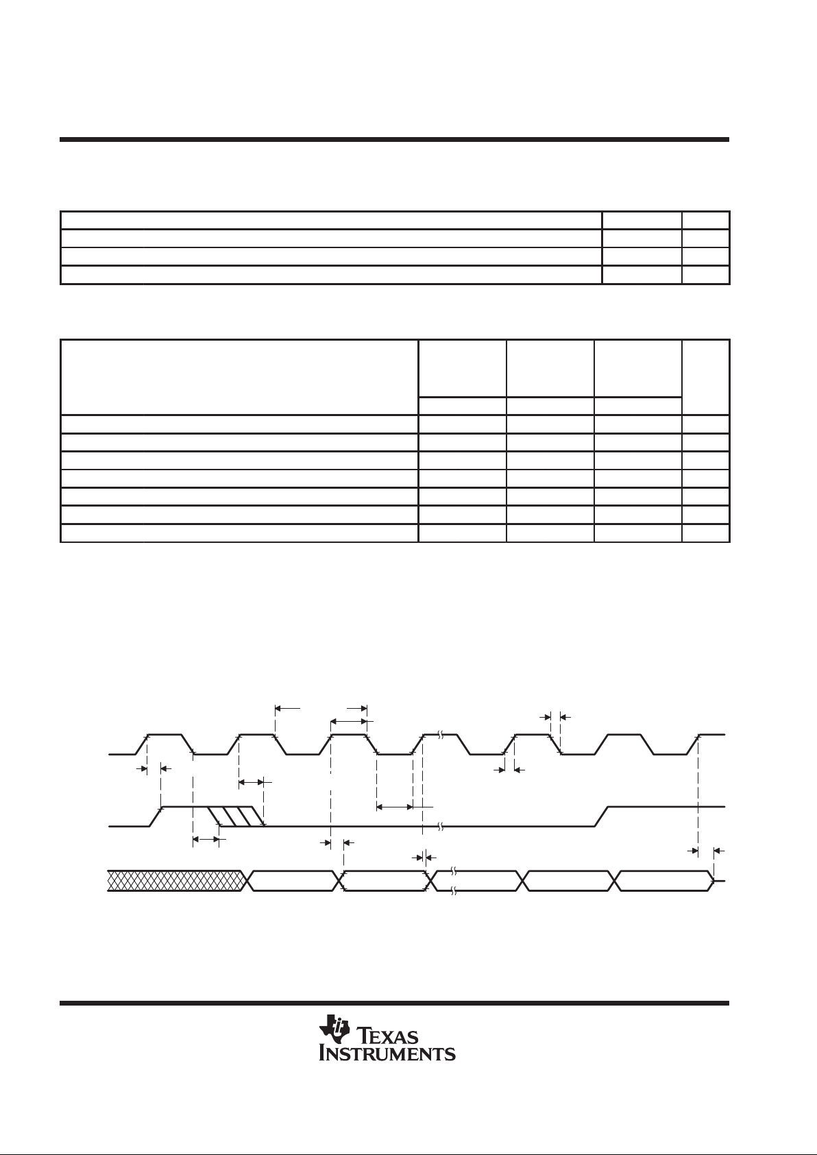
TMS320C5x, TMS320LC5x
DIGITAL SIGNAL PROCESSORS
SPRS030A – APRIL 1995 – REVISED APRIL 1996
70
POST OFFICE BOX 1443 • HOUSTON, TEXAS 77251–1443
SERIAL-PORT TRANSMIT TIMING, EXTERNAL CLOCKS, AND EXTERNAL FRAMES
switching characteristics over recommended operating conditions (see Note 8) (see Figure 23)
PARAMETER MIN MAX UNIT
t
d(CXH-DXV)
Delay time, DX valid after CLKX high 25 ns
t
dis(CXH-DX)
Disable time, DX invalid after CLKX high 40
†
ns
t
h(CXH-DXV)
Hold time, DX valid after CLKX high – 5 ns
timing requirements over recommended ranges of supply voltage and operating ambient-air
temperature [H = 0.5t
c(CO)
] (see Note 8) (see Figure 23)
’320C5x-40
’320C5x-57
’320LC5x-40
’320LC5x-50
’320C5x-80
’320LC5x-80
’320C5x-100
UNIT
MIN MAX MIN MAX MIN MAX
t
c(SCK)
Cycle time, serial-port clock 5.2H
‡
§ 5.2H
‡
§ 5.2H
‡
§ ns
t
f(SCK)
Fall time, serial-port clock 8
†
6
†
6
†
ns
t
r(SCK)
Rise time, serial-port clock 8
†
6
†
6
†
ns
t
w(SCK)
Pulse duration, serial-port clock low/high 2.1H
‡
2.1H
‡
2.1H
‡
ns
t
d(CXH-FXH)
Delay time, FSX high after CLKX high 2H – 8 2H – 8 2H – 5 ns
t
h(CXL-FXL)
Hold time, FSX low after CLKX low 10 7 6 ns
t
h(CXH-FXL)
Hold time, FSX low after CLKX high 2H – 8
¶
2H – 8
¶
2H – 5
¶
ns
†
Values derived from characterization data and not tested
‡
Values ensured by design but not tested
§
The serial-port design is fully static and, therefore, can operate with t
c(SCK)
approaching ∞. It is characterized approaching an input frequency
of 0 Hz but tested at a much higher frequency to minimize test time.
¶
If the FSX pulse does not meet this specification, the first bit of serial data is driven on the DX pin until the falling edge of FSX. After the falling
edge of FSX, data is shifted out on the DX pin. The transmit buffer empty interrupt is generated when the t
h(CXL-FXL)
and t
h(CXH-FXL)
specification
is met.
NOTE 8: Internal clock with external FSX and vice versa are also allowable. However, FSX timings to CLKX always are defined depending on
the source of FSX, and CLKX timings always are dependent on the source of CLKX. Specifically, the relationship of FSX to CLKX is
independent of the source of CLKX.
t
d(CXH-FXH)
DX
BIt
FSX
CLKX
8/167/1521
t
h(CXH-DXV)
t
w(SCK)
t
r(SCK)
t
f(SCK)
t
w(SCK)
t
c(SCK)
t
dis(CXH-DX)
t
h(CXL-FXL)
t
d(CXH-DXV)
t
h(CXH-FXL)
Figure 23. Serial-Port Transmit Timing of External Clocks and External Frames

TMS320C5x, TMS320LC5x
DIGITAL SIGNAL PROCESSORS
SPRS030A – APRIL 1995 – REVISED APRIL 1996
71
POST OFFICE BOX 1443 • HOUSTON, TEXAS 77251–1443
SERIAL-PORT TRANSMIT TIMING, INTERNAL CLOCKS, AND INTERNAL FRAMES
(SEE NOTE 8)
switching characteristics over recommended operating conditions [H = 0.5t
c(CO)
] (see Figure 24)
PARAMETER
’320C5x-40
’320C5x-57
’320LC5x-40
’320LC5x-50
’320C5x-80
’320C5x-100
’320LC5x-80
UNIT
MIN TYP MAX MIN TYP MAX
t
d(CX-FX)
Delay time, CLKX rising edge to FSX –5 25 –4 18 ns
t
d(CX-DX)
Delay time, CLKX rising edge to DX 25 18 ns
t
dis(CX-DX)
Disable time, CLKX rising edge to DX 40
†
29
†
ns
t
c(SCK)
Cycle time, serial-port clock 8H 8H ns
t
f(SCK)
Fall time, serial-port clock 5 4 ns
t
r(SCK)
Rise time, serial-port clock 5 4 ns
t
w(SCK)
Pulse duration, serial-port clock low/high 4H – 20 4H – 14 ns
t
h(CXH-DXV)
Hold time, DX valid after CLKX high –5 –4 ns
†
Values derived from characterization data and not tested
NOTE 8: Internal clock with external FSX and vice versa are also allowable. However, FSX timings to CLKX always are defined depending on
the source of FSX, and CLKX timings always are dependent on the source of CLKX. Specifically, the relationship of FSX to CLKX is
independent of the source of CLKX.
DX
Bit
FSX
CLKX
21
t
h(CXH-DXV)
t
r(SCK)
t
f(SCK)
t
w(SCK)
t
c(SCK)
t
d(CX-FX)
t
d(CX-FX)
t
d(CX-DX)
t
dis(CX-DX)
t
w(SCK)
8/167 /15
Figure 24. Serial-Port Transmit Timing of Internal Clocks and Internal Frames
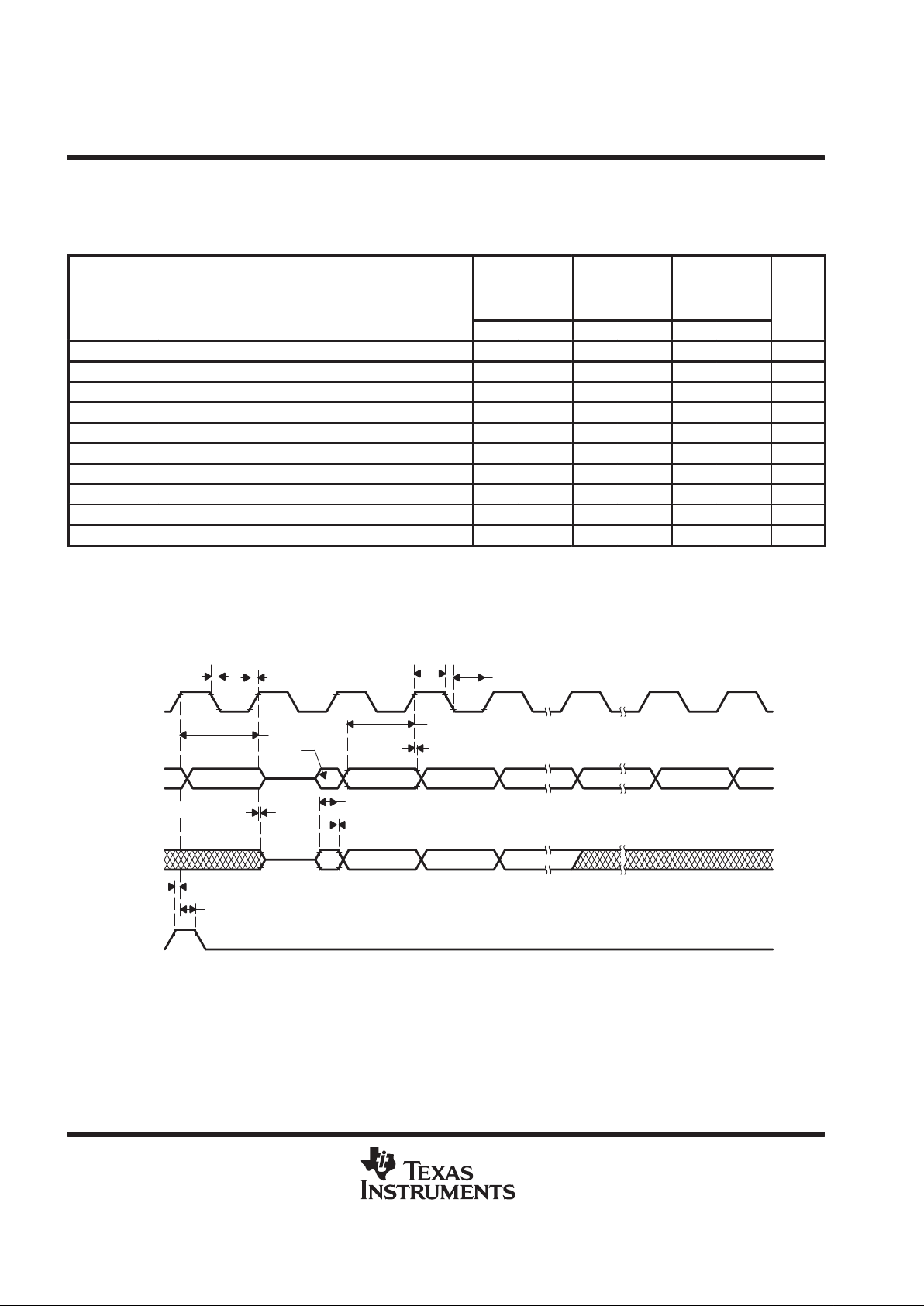
TMS320C5x, TMS320LC5x
DIGITAL SIGNAL PROCESSORS
SPRS030A – APRIL 1995 – REVISED APRIL 1996
72
POST OFFICE BOX 1443 • HOUSTON, TEXAS 77251–1443
SERIAL-PORT RECEIVE TIMING IN TDM MODE
timing requirements over recommended ranges of supply voltage and operating ambient-air
temperature [H = 0.5t
c(CO)
] (see Figure 25)
’320C5x-40
’320C5x-57
’320LC5x-40
’320LC5x-50
’320C5x-80
’320LC5x-80
’320C5x-100
UNIT
MIN MAX MIN MAX MIN MAX
t
c(SCK)
Cycle time, serial-port clock 5.2H
† ‡
5.2H
† ‡
5.2H
§ ‡
ns
t
f(SCK)
Fall time, serial-port clock 8
¶
8
¶
8
¶
ns
t
r(SCK)
Rise time, serial-port clock 8
¶
8
¶
8
¶
ns
t
w(SCK)
Pulse duration, serial-port clock low/high 2.1H
†
2.1H
†
2.1H
†
ns
t
su(TD-TCH)
Setup time, TDAT before TCLK rising edge 30 21 18 ns
t
h(TCH-TD)
Hold time, TDAT after TCLK rising edge –3 –2 –2 ns
t
su(TA-TCH)
Setup time, TADD before TCLK rising edge
#
20 12 10 ns
t
h(TCH-TA)
Hold time, TADD after TCLK rising edge
#
–3 –2 –2 ns
t
su(TF-TCH)
Setup time, TFRM before TCLK rising edge
§
10 10 10 ns
t
h(TCH-TF)
Hold time, TFRM after TCLK rising edge
§
10 10 10 ns
†
Values ensured by design and are not tested
‡
The serial-port design is fully static and, therefore, can operate with t
c(SCK)
approaching ∞. It is characterized approaching an input frequency
of 0 Hz but tested at a much higher frequency to minimize test time.
§
TFRM timing and waveforms shown in Figure 25 are for external TFRM. TFRM also can be configured as internal. The TFRM internal case is
illustrated in the transmit timing diagram in Figure 26.
¶
Values derived from characterization data and not tested
#
These parameters apply only to the first bits in the serial bit string.
A7
B2B8 B7
A3
B12
A2A0 A1
B0B1
B13B14
B15
B0
t
w(SCK)
t
w(SCK)
t
su(TD-TCH)
t
h(TCH-TD)
t
su(TA-TCH)
t
h(TCH-TA)
t
r(SCK)
t
f(SCK)
t
c(SCK)
TFRM
TADD
TDAT
TCLK
t
h(TCH-TF)
t
su(TF-TCH)
t
h(TCH-TA)
Figure 25. Serial-Port Receive Timing in TDM Mode

TMS320C5x, TMS320LC5x
DIGITAL SIGNAL PROCESSORS
SPRS030A – APRIL 1995 – REVISED APRIL 1996
73
POST OFFICE BOX 1443 • HOUSTON, TEXAS 77251–1443
SERIAL-PORT TRANSMIT TIMING IN TDM MODE
switching characteristics over recommended operating conditions [H = 0.5t
c(CO)
] (see Figure 26)
PARAMETER
’320C5x-40
’320C5x-57
’320LC5x-40
’320LC5x-50
’320C5x-80
’320LC5x-80
’320C5x-100
UNIT
MIN MAX MIN MAX MIN MAX
t
h(TCH-TDV)
Hold time, TDAT/TADD valid after TCLK rising edge 0 0 0 ns
t
d(TCH-TFV)
Delay time, TFRM valid after TCLK rising edge
†
H 3H + 10 H 3H + 7 3H + 5 ns
t
d(TC-TDV)
Delay time, TCLK to valid TDAT/TADD 20 15 12 ns
†
TFRM timing and waveforms shown in Figure 28 are for internal TFRM. TFRM can also be configured as external. The TFRM external case is
illustrated in the receive timing diagram in Figure 27.
timing requirements over recommended ranges of supply voltage and operating ambient-air
temperature [H = 0.5t
c(CO)
] (see Figure 26)
’320C5x-40
’320C5x-57
’320LC5x-40
’320LC5x-50
’320C5x-80
’320LC5x-80
’320C5x-100
UNIT
MIN TYP MAX MIN TYP MAX MIN TYP MAX
t
c(SCK)
Cycle time, serial-port clock 5.2H‡8H
§ ¶
5.2H‡8H
§ ¶
5.2H‡8H
§ ¶
ns
t
f(SCK)
Fall time, serial-port clock 8# 6# 5# ns
t
r(SCK)
Rise time, serial-port clock 8# 6# 5# ns
t
w(SCK)
Pulse duration, serial-port clock low/
high
2.1H
‡
2.1H
‡
2.1H
‡
ns
‡
Values ensured by design and are not tested
§
When SCK is generated internally
¶
The serial-port design is fully static and, therefore, can operate with t
c(SCK)
approaching ∞. It is characterized approaching an input frequency
of 0 Hz but tested as a much higher frequency to minimize test time.
#
Values derived from characterization data and not tested
A7
B2B8 B7
A3
B12
A2
A0
A1
B0B1
B13B14B0
t
w(SCK)
t
w(SCK)
t
d(TC-TDV)
t
h(TCH-TDV)
t
r(SCK)
t
f(SCK)
t
d(TCH-TFV)
TFRM
TADD
TDAT
TCLK
B15
t
c(SCK)
t
d(TC-TDV)
t
h(TCH-TDV)
t
d(TCH-TFV)
Figure 26. Serial-Port Transmit Timing in TDM Mode

TMS320C5x, TMS320LC5x
DIGITAL SIGNAL PROCESSORS
SPRS030A – APRIL 1995 – REVISED APRIL 1996
74
POST OFFICE BOX 1443 • HOUSTON, TEXAS 77251–1443
BUFFERED SERIAL-PORT RECEIVE TIMING
timing requirements over recommended ranges of supply voltage and operating ambient-air
temperature [H = 0.5t
c(CO)
] (see Figure 27)
MIN MAX UNIT
t
c(SCK)
Cycle time, serial-port clock 25
†
ns
t
f(SCK)
Fall time, serial-port clock 6
‡
ns
t
r(SCK)
Rise time, serial-port clock 6
‡
ns
t
w(SCK)
Pulse duration, serial-port clock low/high 12 ns
t
su(FS-CK)
Setup time, FSR before CLKR falling edge 2 ns
t
su(DR-CK)
Setup time, DR before CLKR falling edge 0 ns
t
h(CK-FS)
Hold time, FSR after CLKR falling edge 12 t
c(SCK)
§
ns
t
h(CK-DR)
Hold time, DR after CLKR falling edge 15 ns
†
The serial-port design is fully static and, therefore, can operate with t
c(SCK)
approaching ∞. It is characterized approaching an input frequency
of 0 Hz but tested at a much higher frequency to minimize test time.
‡
Values derived from characterization data and not tested
§
First bit is read when FSR is sampled low by CLKR clock.
Bit
DR
FSR
CLKR
8/167/1521
t
su(DR-CK)
t
su(FS-CK)
t
h(CK-FS)
t
w(SCK)
t
r(SCK)
t
f(SCK)
t
w(SCK)
t
h(CK-DR)
t
c(SCK)
Figure 27. Buffered Serial-Port Receive Timing

TMS320C5x, TMS320LC5x
DIGITAL SIGNAL PROCESSORS
SPRS030A – APRIL 1995 – REVISED APRIL 1996
75
POST OFFICE BOX 1443 • HOUSTON, TEXAS 77251–1443
BUFFERED SERIAL-PORT TRANSMIT TIMING OF EXTERNAL FRAMES (SEE NOTES 9 AND 10)
switching characteristics over recommended operating conditions (see Figure 28)
PARAMETER MIN MAX UNIT
t
d(CXH-DXV)
Delay time, DX valid after CLKX rising edge 5 21 ns
t
dis(CXH-DX)
Disable time, DX invalid after CLKX rising edge 5 15 ns
t
dis(CXH-DX)PCM
Disable time in PCM mode, DX invalid after CLKX rising edge 15 ns
t
en(CXH-DX)PCM
Enable time in PCM mode, DX valid after CLKX rising edge 21 ns
t
h(CXH-DXV)
Hold time, DX valid after CLKX rising edge 5 20 ns
timing requirements over recommended operating conditions (see Figure 28)
MIN MAX UNIT
t
c(SCK)
Cycle time, serial-port clock 25
†
ns
t
f(SCK)
Fall time, serial-port clock 4
‡
ns
t
r(SCK)
Rise time, serial-port clock 4
‡
ns
t
w(SCK)
Pulse duration, serial-port clock low/high 8.5 ns
t
su(FX-CXL)
Setup time, FSX before CLKX falling edge 5 ns
t
h(CXL-FX)
Hold time, FSX after CLKX falling edge 5 t
c(SCK)
–5
§
ns
†
The serial-port design is fully static and, therefore, can operate with t
c(SCK)
approaching ∞. It is characterized approaching an input frequency
of 0 Hz but tested at a much higher frequency to minimize test time.
‡
Values derived from characterization data and not tested
§
If the FSX pulse does not meet this specification, the first bit of the serial data is driven on the DX pin until FSX goes low (sampled on falling edge
of CLKX). After falling edge of the FSX, data is shifted out on the DX pin.
NOTE 9: Internal clock with external FSX and vice versa are also allowable. However, FSX timings to CLKX always are defined depending on
the source of FSX, and CLKX timings always are dependent upon the source of CLKX. Specifically, the relationship of FSX to CLKX
is independent of the source of CLKX. External FSX timings are obtained from the “timing requirements over recommended operating
conditions” table listed in the “Buffered Serial-Port Transmit T iming of External Frames” section and internal FSX timings are obtained
from the “switching characteristics over recommended operating conditions” table listed under the “Buffered Serial-Port Transmit T iming
of Internal Frame and Internal Clock” section. Internal CLKX timings are obtained from the “switching characteristics over recommended
operating conditions” table listed under the “Buffered Serial-Port Transmit Timing of Internal Frame and Internal Clock” section and
external CLKX timings are obtained from the “timing requirements over recommended operating conditions” table in the “Buffered
Serial-Port Transmit Timing of External Frames” section.
NOTE 10: Timings for CLKX and FSX are given with polarity bits (CLKP and FSP) set to 0
DX BIt
FSX
CLKX
8/167/1521
t
h(CXH-DXV)
t
d(CXH-DXV)
t
w(SCK)
t
r(SCK)
t
f(SCK)
t
w(SCK)
t
c(SCK)
t
h(CXL-FX)
t
dis(CXH-DX)
t
su(FX-CXL)
Figure 28. Buffered Serial-Port Transmit Timing of External Clocks and External Frames

TMS320C5x, TMS320LC5x
DIGITAL SIGNAL PROCESSORS
SPRS030A – APRIL 1995 – REVISED APRIL 1996
76
POST OFFICE BOX 1443 • HOUSTON, TEXAS 77251–1443
BUFFERED SERIAL-PORT TRANSMIT TIMING OF INTERNAL FRAME AND INTERNAL CLOCK
(SEE NOTES 9 AND 10)
switching characteristics over recommended operating conditions [H = 0.5t
c(CO)
] (see Figure 29)
PARAMETER MIN MAX UNIT
t
d(CXH-FXH)
Delay time, FSX high after CLKX rising edge 10 ns
t
d(CXH-FXL)
Delay time, FSX low after CLKX rising edge 10 ns
t
d(CXH-DXV)
Delay time, DX valid after CLKX rising edge 5 10 ns
t
dis(CXH-DX)
Disable time, DX invalid after CLKX rising edge 4 8 ns
t
dis(CXH-DX)PCM
Disable time in PCM mode, DX invalid after CLKX rising edge 10 ns
t
en(CXH-DX)PCM
Enable time in PCM mode, DX valid after CLKX rising edge 16 ns
t
c(SCK)
Cycle time, serial-port clock 2H 62H ns
t
f(SCK)
Fall time, serial-port clock 4
†
ns
t
r(SCK)
Rise time, serial-port clock 4
†
ns
t
w(SCK)
Pulse duration, serial-port clock low/high H–4 ns
t
h(CXH-DXV)
Hold time, DX valid after CLKX rising edge 4 8 ns
†
Values derived from characterization data and not tested
NOTES: 9. Internal clock with external FSX and vice versa are also allowable. However, FSX timings to CLKX always are defined depending
on the source of FSX, and CLKX timings always are dependent upon the source of CLKX. Specifically, the relationship of FSX to
CLKX is independent of the source of CLKX. External FSX timings are obtained from the “timing requirements over recommended
operating conditions” table listed in the “Buffered Serial-Port Transmit T iming of External Frames” section and internal FSX timings
are obtained from the “switching characteristics over recommended operating conditions” table listed under the “Buffered Serial-Port
Transmit Timing of Internal Frame and Internal Clock” section. Internal CLKX timings are obtained from the “switching characteristics
over recommended operating conditions” table listed under the “Buffered Serial-Port Transmit Timing of Internal Frame and Inter nal
Clock” section and external CLKX timings are obtained from the “timing requirements over recommended operating conditions” table
in the “Buffered Serial-Port Transmit Timing of External Frames” section.
10. Timings for CLKX and FSX are given with polarity bits (CLKP and FSP) set to 0.
DX
Bit
FSX
CLKX
21
t
h(CXH-DXV)
t
r(SCK)
t
f(SCK)
t
w(SCK)
t
c(SCK)
t
d(CXH-FXL)
t
d(CXH-DXV)
t
dis(CXH-DX)
t
w(SCK)
8/167 /15
t
d(CXH-FXH)
Figure 29. Buffered Serial-Port Transmit Timing of Internal Clocks and Internal Frames

TMS320C5x, TMS320LC5x
DIGITAL SIGNAL PROCESSORS
SPRS030A – APRIL 1995 – REVISED APRIL 1996
77
POST OFFICE BOX 1443 • HOUSTON, TEXAS 77251–1443
HOST PORT INTERFACE (TMS320C57S, TMS320LC57 ONLY)
switching characteristics over recommended operating conditions [H = 0.5t
c(CO)
] (See Notes 1 1
and 12) (see Figure 30 through Figure 33)
PARAMETER MIN MAX UNIT
t
d(DSL-HDV)
Delay time, DS low to HD valid 5 ns
t
d(HEL-HDV1)
Delay time, HDS falling to HD valid for first byte of a subsequent read:
Case 1: Shared-access mode if t
w(HDS
)h
< 7H † ‡
Case 2: Shared-access mode if t
w(HDS
)h
> 7H
Case 3: Host-only mode if t
w(HDS
)h
< 7H
Case 4: Host-only mode if t
w(HDS
)h
> 7H
7H+20–t
w(DSH)
20
40–t
w(DSH)
20
ns
t
d(DSL-HDV2)
Delay time, DS low to HD valid, second byte 20 ns
t
d(DSH-HYH)
Delay time, DS high to HRDY high ns
t
su(HDV-HYH)
Setup time, HD valid before HRDY rising edge 3H–10 ns
t
h(DSH-HDV)
Hold time, HD valid after DS rising edge 0 12
§
ns
t
d(COH-HYH)
Delay time, CLKOUT rising edge to HRDY high 10 ns
t
d(DSH-HYL)
Delay time, HDS or HCS high to HRDY low 12 ns
t
d(COH-HTX)
Delay time, CLKOUT rising edge to HINT change 10 ns
†
Host-only mode timings apply for read accesses to HPIC or HPIA, write accesses to BOB, and resetting DSPINT or HINT to 0 in shared-access
mode. HRDY does not go low for these accesses.
‡
Shared-access mode timings are met automatically if HRDY is used.
§
HD release
NOTES: 11. SAM = shared-access mode, HOM = host-only mode
HAD stands for HCNTRL0, HCNTRL1, and HR/W
.
HDS
refers to either HDS1 or HDS2.
DS refers to the logical OR of HCS and HDS.
12. On host-read accesses to the HPI, the setup time of HD before DS rising edge depends on the host waveforms and cannot be
specified here.
timing requirements over recommended operating conditions [H = 0.5t
c(CO)
] (See Note 11)
(see Figure 30 through Figure 33)
MIN MAX UNIT
t
su(HBV-DSL)
Setup time, HAD/HBIL valid before HAS or DS falling edge
#
10 ns
t
h(DSL-HBV)
Hold time, HAD/HBIL valid after HAS or DS falling edge
#
10 ns
t
su(HSL-DSL)
Setup time, HAS low before DS falling edge 10 ns
t
w(DSL)
Pulse duration, DS low 25 ns
t
w(DSH)
Pulse duration, DS high 10 ns
t
c(DSH-DSH)
Cycle time, DS rising edge to next DS rising edge:
Case 1: When using HRDY (see Figure 32)
Case 2a: SAM accesses and HOM active writes to DSPINT or HINT without using HRDY
(see Figure 30 and Figure 31)
Case 2b: When not using HRDY for other HOM accesses
50
10H
¶
50
ns
t
su(HDV-DSH)
Setup time, HD valid before DS rising edge 10 ns
t
h(DSH-HDV)
Hold time, HD valid after DS rising edge 0 ns
¶
A host not using HRDY must meet the 10 H requirement all the time unless a software handshake is used to change the access rate according
to the HPI mode.
#
When HAS
is tied to VDD, timing is referenced to DS.
NOTE 11: SAM = shared-access mode, HOM = host-only mode
HAD stands for HCNTRL0, HCNTRL1, and HR/W
.
HDS
refers to either HDS1 or HDS2.
DS
refers to the logical OR of HCS and HDS.

TMS320C5x, TMS320LC5x
DIGITAL SIGNAL PROCESSORS
SPRS030A – APRIL 1995 – REVISED APRIL 1996
78
POST OFFICE BOX 1443 • HOUSTON, TEXAS 77251–1443
HOST PORT INTERFACE (TMS320C57S, TMS320LC57 ONLY) (CONTINUED)
HBIL
HAD
t
h(DSL-HBV)
t
su(HBV-DSL)
t
h(DSL-HBV)
FIRST BYTE SECOND BYTE
HCS
HDS
t
w(DSL)
t
c(DSH-DSH)
HD
READ
t
h(DSH-HDV)
t
h(DSH-HDV)
HD
WRITE
t
h(DSH-HDV)
t
su(HDV-DSH)
t
su(HBV-DSL)
t
d(DSL-HDV2)
t
w(DSH)
t
w(DSH)
t
w(DSL)
t
h(DSH-HDV)
t
su(HDV-DSH)
Valid
Valid Valid
Valid Valid
Valid
Valid
t
d(HEL-HDV1)
t
d(DSL-HDV)
Figure 30. Read/Write Access Timings Without HRDY or HAS

TMS320C5x, TMS320LC5x
DIGITAL SIGNAL PROCESSORS
SPRS030A – APRIL 1995 – REVISED APRIL 1996
79
POST OFFICE BOX 1443 • HOUSTON, TEXAS 77251–1443
HOST PORT INTERFACE (TMS320C57S, TMS320LC57 ONLY) (CONTINUED)
FIRST BYTE SECOND BYTE
HAD
t
su(HSL-DSL)
t
h(DSL-HBV)
HBIL
t
c(DSH-DSH)
HCS
HDS
HAS
t
w(DSL)
t
c(DSH-DSH)
HD
READ
t
h(DSH-HDV)
t
h(DSH-HDV)
HD
WRITE
t
h(DSH-HDV)
Valid Valid
Valid
Valid
t
d(DSL-HDV2)
t
su(HDV-DSH)t
su(HDV-DSH)
t
w(DSH)
t
d(DSL-HDV)
t
d(HEL-HDV1)
t
h(DSH-HDV)
t
su(HBV-DSL)
Valid Valid Valid
Figure 31. Read/Write Access Timings Using HAS Without HRDY

TMS320C5x, TMS320LC5x
DIGITAL SIGNAL PROCESSORS
SPRS030A – APRIL 1995 – REVISED APRIL 1996
80
POST OFFICE BOX 1443 • HOUSTON, TEXAS 77251–1443
HOST PORT INTERFACE (TMS320C57S, TMS320LC57 ONLY) (CONTINUED)
FIRST BYTE SECOND BYTE
t
h(DSL-HBV)
†
HRDY
t
d(DSH-HYL)
CLKOUT
t
d(COH-HYH)
HINT
t
d(COH-HTX)
†
When HAS
is tied to V
DD
t
su(HBV-DSL)
†
t
su(HSL-DSL)
t
h(DSL-HBV)
HCS
HDS
HAS
t
w(DSL)
t
c(DSH-DSH)
HD
READ
t
h(DSH-HDV)
t
h(DSH-HDV)
HD
WRITE
t
h(DSH-HDV)
t
h(DSH-HDV)
Valid Valid
Valid
Valid
t
su(HDV-DSH)
t
su(HDV-DSH)
t
w(DSH)
t
d(DSL-HDV2)
HAD
HBIL
t
su(HDV-HYH)
t
d(DSH-HYH)
t
su(HBV-DSL)
t
d(DSL-HDV)
t
d(HEL-HDV1)
Figure 32. Read/Write Access Timing With HRDY

TMS320C5x, TMS320LC5x
DIGITAL SIGNAL PROCESSORS
SPRS030A – APRIL 1995 – REVISED APRIL 1996
81
POST OFFICE BOX 1443 • HOUSTON, TEXAS 77251–1443
HOST PORT INTERFACE (TMS320C57S, TMS320LC57 ONLY) (CONTINUED)
HRDY
HCS
t
d(DSH-HYL)
t
d(DSH-HYH)
HDS
Figure 33. HRDY Signal When HCS Is Always Low

TMS320C5x, TMS320LC5x
DIGITAL SIGNAL PROCESSORS
SPRS030A – APRIL 1995 – REVISED APRIL 1996
82
POST OFFICE BOX 1443 • HOUSTON, TEXAS 77251–1443
MECHANICAL DATA
PQ (S-PQFP-G132) PLASTIC QUAD FLATPACK
116
0.012 (0,30)
0.008 (0,20)
84
0.025 (0,635)
Seating Plane
0.966 (24,54)
0.934 (23,72)
1.112 (28,25)
1.088 (27,64)
0.800
(20,32)
SQ
132117
8351
SQ
SQ
18
50
0.180 (4,57) MAX
0.004 (0,10)
M
0.006 (0,15)
0.020
(0,51) MIN
0.130 (3,30)
0.150 (3,81)
0.006
(0,16)
NOM
Gage Plane
0.036 (0,91)
0.046 (1,17)
0°–8°
117
0.010 (0,25)
1.090 (27,69)
1.070 (27,18)
SQ
NOTES: A. All linear dimensions are in inches (millimeters).
B. This drawing is subject to change without notice.
C. Falls within JEDEC MO-069
Thermal Resistance Characteristics
PARAMETER
°C/W
R
ΘJA
35
R
ΘJC
8.5

TMS320C5x, TMS320LC5x
DIGITAL SIGNAL PROCESSORS
SPRS030A – APRIL 1995 – REVISED APRIL 1996
83
POST OFFICE BOX 1443 • HOUSTON, TEXAS 77251–1443
MECHANICAL DATA
PBK/S-PQFP-G128 PLASTIC QUAD FLATPACK
4040279-3/B 10/94
64
33
Gage Plane
0,13 NOM
0,25
0,45
0,75
Seating Plane
0,05 MIN
0,23
65
32
96
1
11,60 TYP
0,13
97
128
SQ
SQ
13,80
16,20
15,80
1,60 MAX
1,45
1,35
14,20
0°–7°
0,08
0,40
M
0,07
NOTES: A. All linear dimensions are in millimeters.
B. This drawing is subject to change without notice.
Thermal Resistance Characteristics
PARAMETER
°C/W
R
ΘJA
58
R
ΘJC
10

TMS320C5x, TMS320LC5x
DIGITAL SIGNAL PROCESSORS
SPRS030A – APRIL 1995 – REVISED APRIL 1996
84
POST OFFICE BOX 1443 • HOUSTON, TEXAS 77251–1443
MECHANICAL DATA
PJ (R-PQFP-G100) PLASTIC QUAD FLA TPACK
4040012/B 10/94
0,15 NOM
18,0014,20
17,2013,80
50
51
31
30
12,35 TYP
0,25
0,70
1,10
0,10 MIN
Gage Plane
80
1
18,85 TYP
81
100
20,20
19,80
23,20
24,00
3,10 MAX
2,70 TYP
0,20
0,40
Seating Plane
0,15
0,65
M
0,13
0°–10°
NOTES: A. All linear dimensions are in millimeters.
B. This drawing is subject to change without notice.
C. Contact field sales office to determine if a tighter coplanarity requirement is available for this package.
Thermal Resistance Characteristics
PARAMETER
°C/W
R
ΘJA
78
R
ΘJC
13

TMS320C5x, TMS320LC5x
DIGITAL SIGNAL PROCESSORS
SPRS030A – APRIL 1995 – REVISED APRIL 1996
85
POST OFFICE BOX 1443 • HOUSTON, TEXAS 77251–1443
MECHANICAL DATA
PZ (S-PQFP-G100) PLASTIC QUAD FLATPACK
4040149/B 10/94
50
26
0,13 NOM
Gage Plane
0,25
0,45
0,75
0,05 MIN
0,27
51
25
75
1
12,00 TYP
0,17
76
100
SQ
SQ
15,80
16,20
13,80
1,35
1,45
1,60 MAX
14,20
0°–7°
Seating Plane
0,08
0,50
M
0,08
NOTES: A. All linear dimensions are in millimeters.
B. This drawing is subject to change without notice.
C. Falls within JEDEC MO-136
Thermal Resistance Characteristics
PARAMETER
°C/W
R
ΘJA
58
R
ΘJC
10

TMS320C5x, TMS320LC5x
DIGITAL SIGNAL PROCESSORS
SPRS030A – APRIL 1995 – REVISED APRIL 1996
86
POST OFFICE BOX 1443 • HOUSTON, TEXAS 77251–1443
MECHANICAL DATA
PGE (S-PQFP-G144) PLASTIC QUAD FLATPACK
4040147/B 10/94
0,27
72
0,17
37
73
0,13 NOM
0,25
0,75
0,45
0,05 MIN
36
Seating Plane
Gage Plane
108
109
144
SQ
SQ
22,20
21,80
1
19,80
17,50 TYP
20,20
1,35
1,45
1,60 MAX
M
0,08
0°–7°
0,08
0,50
NOTES: A. All linear dimensions are in millimeters.
B. This drawing is subject to change without notice.
C. Falls within JEDEC MO-136
Thermal Resistance Characteristics
PARAMETER
°C/W
R
ΘJA
40
R
ΘJC
9.9

IMPORTANT NOTICE
T exas Instruments and its subsidiaries (TI) reserve the right to make changes to their products or to discontinue
any product or service without notice, and advise customers to obtain the latest version of relevant information
to verify, before placing orders, that information being relied on is current and complete. All products are sold
subject to the terms and conditions of sale supplied at the time of order acknowledgement, including those
pertaining to warranty, patent infringement, and limitation of liability.
TI warrants performance of its semiconductor products to the specifications applicable at the time of sale in
accordance with TI’s standard warranty. Testing and other quality control techniques are utilized to the extent
TI deems necessary to support this warranty. Specific testing of all parameters of each device is not necessarily
performed, except those mandated by government requirements.
CERT AIN APPLICATIONS USING SEMICONDUCTOR PRODUCTS MAY INVOLVE POTENTIAL RISKS OF
DEATH, PERSONAL INJURY, OR SEVERE PROPERTY OR ENVIRONMENTAL DAMAGE (“CRITICAL
APPLICATIONS”). TI SEMICONDUCTOR PRODUCTS ARE NOT DESIGNED, AUTHORIZED, OR
WARRANTED TO BE SUITABLE FOR USE IN LIFE-SUPPORT DEVICES OR SYSTEMS OR OTHER
CRITICAL APPLICATIONS. INCLUSION OF TI PRODUCTS IN SUCH APPLICA TIONS IS UNDERSTOOD T O
BE FULLY AT THE CUSTOMER’S RISK.
In order to minimize risks associated with the customer’s applications, adequate design and operating
safeguards must be provided by the customer to minimize inherent or procedural hazards.
TI assumes no liability for applications assistance or customer product design. TI does not warrant or represent
that any license, either express or implied, is granted under any patent right, copyright, mask work right, or other
intellectual property right of TI covering or relating to any combination, machine, or process in which such
semiconductor products or services might be or are used. TI’s publication of information regarding any third
party’s products or services does not constitute TI’s approval, warranty or endorsement thereof.
Copyright 1998, Texas Instruments Incorporated
 Loading...