

Texas Instruments TMS320LC549PGE-80, TMS320LC549PGE-66, TMS320LC549GGU-80, TMS320LC549GGU-66 Datasheet

TMS320LC549
FIXED-POINT DIGITAL SIGNAL PROCESSOR
SPRS077B – SEPTEMBER 1998 – REVISED FEBRUARY 2000
1
POST OFFICE BOX 1443 • HOUSTON, TEXAS 77251–1443
D Advanced Multibus Architecture With Three
Separate 16-Bit Data Memory Buses and
One Program Memory Bus
D 40-Bit Arithmetic Logic Unit (ALU)
Including a 40-Bit Barrel Shifter and Two
Independent 40-Bit Accumulators
D 17- × 17-Bit Parallel Multiplier Coupled to a
40-Bit Dedicated Adder for Non-Pipelined
Single-Cycle Multiply/Accumulate (MAC)
Operation
D Compare, Select, and Store Unit (CSSU) for
the Add/Compare Selection of the Viterbi
Operator
D Exponent Encoder to Compute an
Exponent Value of a 40-Bit Accumulator
Value in a Single Cycle
D T wo Address Generators With Eight
Auxiliary Registers and Two Auxiliary
Register Arithmetic Units (ARAUs)
D Data Bus With a Bus Holder Feature
D Address Bus With a Bus Holder Feature
D Extended Addressing Mode for 8M × 16-Bit
Maximum Addressable External Program
Space
D 192K × 16-Bit Maximum Addressable
Memory Space (64K Words Program,
64K Words Data, and 64K Words I/O)
D On-Chip ROM with Some Configurable to
Program/Data Memory
D Dual-Access On-Chip RAM
D Single-Access On-Chip RAM
D Single-Instruction Repeat and
Block-Repeat Operations for Program Code
D Block-Memory-Move Instructions for Better
Program and Data Management
D Instructions With a 32-Bit Long Word
Operand
D Instructions With Two- or Three-Operand
Reads
D Arithmetic Instructions With Parallel Store
and Parallel Load
D Conditional Store Instructions
D Fast Return From Interrupt
D On-Chip Peripherals
– Software-Programmable Wait-State
Generator and Programmable Bank
Switching
– On-Chip Phase-Locked Loop (PLL) Clock
Generator With Internal Oscillator or
External Clock Source
– Time-Division Multiplexed (TDM) Serial
Port
– Buffered Serial Port (BSP)
– 8-Bit Parallel Host-Port Interface (HPI)
– One 16-Bit Timer
– External-Input/Output (XIO) Off Control
to Disable the External Data Bus,
Address Bus and Control Signals
D Power Consumption Control With IDLE1,
IDLE2, and IDLE3 Instructions With
Power-Down Modes
D CLKOUT Off Control to Disable CLKOUT
D On-Chip Scan-Based Emulation Logic,
IEEE Std 1149.1† (JTAG) Boundary Scan
Logic
D 15-ns Single-Cycle Fixed-Point Instruction
Execution Time (66 MIPS) for 3.3-V Power
Supply
D 12.5-ns Single-Cycle Fixed-Point
Instruction Execution Time (80 MIPS) for
3.3-V Power Supply
Please be aware that an important notice concerning availability, standard warranty, and use in critical applications of
Texas Instruments semiconductor products and disclaimers thereto appears at the end of this data sheet.
Copyright 2000, Texas Instruments Incorporated
†
IEEE Standard 1149.1-1990 Standard-Test-Access Port and Boundary Scan Architecture.
PRODUCTION DATA information is current as of publication date.
Products conform to specifications per the terms of Texas Instruments
standard warranty. Production processing does not necessarily include
testing of all parameters.

TMS320LC549
FIXED-POINT DIGITAL SIGNAL PROCESSOR
SPRS077B – SEPTEMBER 1998 – REVISED FEBRUARY 2000
2
POST OFFICE BOX 1443 • HOUSTON, TEXAS 77251–1443
Table of Contents
Description 2. . . . . . . . . . . . . . . . . . . . . . . . . . . . . . . . . . .
Pin Assignments 5. . . . . . . . . . . . . . . . . . . . . . . . . . . . . .
Signal Descriptions 6. . . . . . . . . . . . . . . . . . . . . . . . . . .
Absolute Maximum Ratings 1 1. . . . . . . . . . . . . . . . . . . .
Recommended Operating Conditions 1 1. . . . . . . . . . .
Timing Parameter Symbology 12. . . . . . . . . . . . . . . . . .
Electrical Characteristics 13. . . . . . . . . . . . . . . . . . . . . .
Divide-by-Two/Divide-by-Four Clock Option 15. . . . . .
Multiply-by-N Clock Option 17. . . . . . . . . . . . . . . . . . . . .
Memory and Parallel I/O Interface Timing 19. . . . . . . .
Timing Requirements for a Memory Read 20. . . . . . .
I/O Timing Variation: SPICE Simulation 27. . . . . . . . . .
Timing For Externally Generated Wait States 30. . . . .
HOLD and HOLDA Timings 35. . . . . . . . . . . . . . . . . . . .
Reset, BIO, Interrupt, and MP/MC Timings 37. . . . . . .
Serial Port Receive Timing 41. . . . . . . . . . . . . . . . . . . . .
Serial Port Transmit Timing 42. . . . . . . . . . . . . . . . . . . .
Buffered Serial Port Receive Timing 44. . . . . . . . . . . . .
Buffered Serial Port Transmit Timing 45. . . . . . . . . . . .
Serial-Port Receive Timing in TDM Mode 48. . . . . . . .
Serial-Port Transmit Timing in TDM Mode 50. . . . . . . .
Host-Port Interface Timing 52. . . . . . . . . . . . . . . . . . . . .
Mechanical Data 59. . . . . . . . . . . . . . . . . . . . . . . . . . . . .
description
The TMS320LC549 fixed-point, digital signal processor (DSP) (hereafter referred to as the ’549) is based on
an advanced modified Harvard architecture that has one program memory bus and three data memory buses.
The processor also provides an arithmetic logic unit (ALU) that has a high degree of parallelism,
application-specific hardware logic, on-chip memory , and additional on-chip peripherals. The ’549 also utilizes
a highly specialized instruction set, which is the basis of its operational flexibility and speed.
Separate program and data spaces allow simultaneous access to program instructions and data, providing the
high degree of parallelism. Two reads and one write operation can be performed in a single cycle. Instructions
with parallel store and application-specific instructions can fully utilize this architecture. In addition, data can be
transferred between data and program spaces. Such parallelism supports a powerful set of arithmetic, logic,
and bit-manipulation operations that can all be performed in a single machine cycle. In addition, the ’549
includes the control mechanisms to manage interrupts, repeated operations, and function calls.
This data sheet contains the pin layouts, signal descriptions, and electrical specifications for the TMS320VC549
DSP. For additional information, see the
TMS320C54x, TMS320LC54x, TMS320VC54x Fixed-Point Digital
Signal Processors
data sheet (literature number SPRS039). The SPRS039 is considered a family functional
overview and should be used in conjunction with this data sheet.
TMS320LC549
FIXED-POINT DIGITAL SIGNAL PROCESSOR
SPRS077B – SEPTEMBER 1998 – REVISED FEBRUARY 2000
3
POST OFFICE BOX 1443 • HOUSTON, TEXAS 77251–1443
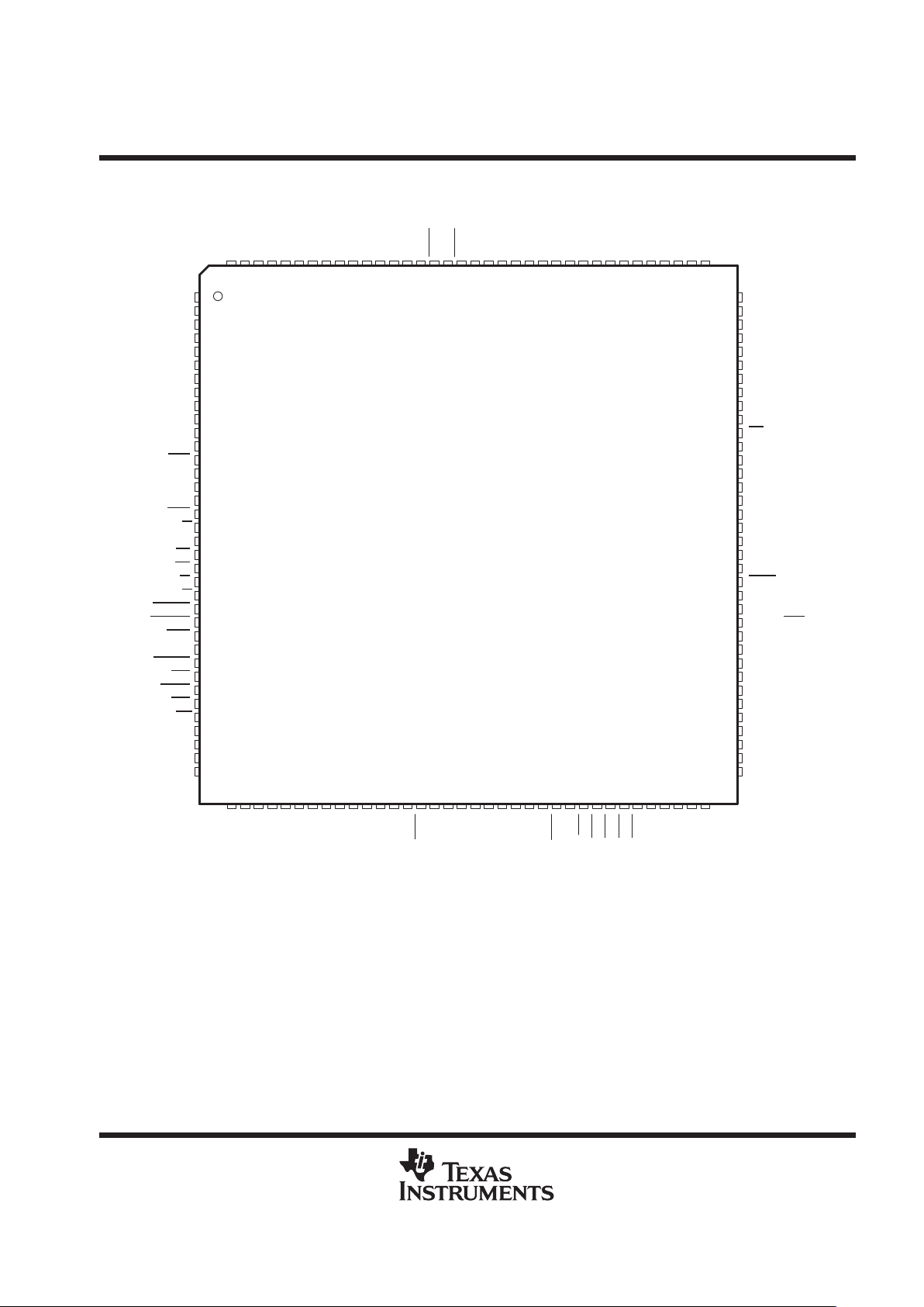
CV
HDS1
A18
A17
VSS
A16
D5
D4
D3
D2
D1
D0
RS
X2/CLKIN
X1
HD3
CLKOUT
V
SS
HPIENA
CV
DD
V
SS
TMS
TCK
TRST
TDI
TDO
EMU1/OFF
EMU0
TOUT
HD2
TEST1
CLKMD3
CLKMD2
CLKMD1
V
SS
DV
DD
BDX1
BFSX1
V
SS
A22
V
SS
DV
DD
A10
HD7
A11
A12
A13
A14
A15
CV
DD
HAS
V
SS
V
SS
CV
DD
HCS
HR/W
READY
PS
DS
IS
R/W
MSTRB
IOSTRB
MSC
XF
HOLDA
IAQ
HOLD
BIO
MP/MC
DV
DD
V
SS
BDR1
BFSR1
SS
V
144
A21
CV
143
142
141A8140A7139A6138A5137A4136
HD6
135A3134A2133A1132A0131DV130
129
128
127V126
125
HD5
124
D15
123
D14
122
D13
121
HD4
120
D12
119
D11
118
117D9116D8115D7114D6113
112
373839404142434445464748495051525354555657585960616263646566676869
1
2
3
4
5
6
7
8
9
10
11
12
13
14
15
16
17
18
19
20
21
22
23
24
25
26
27
28
29
30
31
32
33
34
35
36
108
107
106
105
104
103
102
101
100
99
98
97
96
95
94
93
92
91
90
89
88
87
86
85
84
83
82
81
80
79
78
77
76
75
74
73
SS
V
BCLKR1
HCNTL0SSBCLKR0
TCLKR
BFSR0
TFSR/TADD
BDR0
HCNTL1
TDR
BCLKX0
TCLKX
SS
DD
SS
HD0
BDX0
TDX
IACK
HBIL
NMI
INT0
INT1
INT2
INT3
DD
HD1
SS
HRDY
HINT
111
V
110
A19
109
707172
BCLKX1
SS
V
D10
TFSX/TFRM
SS
A20
DV
DD
CV
HDS2SSV
V
V
DV
V
CV
V
DD
DD
DD
DD
SS
PGE PACKAGE
†‡
(TOP VIEW)
BFSX0
A9
†
NC = No connection
‡
DVDD is the power supply for the I/O pins while CVDD is the power supply for the core CPU, and VSS is the ground for both the I/O pins and the
core CPU.
The ’549 signal descriptions table lists each terminal name, function, and operating mode(s) for the 144-pin thin
quad flatpack (TQFP).
The letter B in front of CLKRn, FSRn, DRn, CLKXn, FSXn, and DXn pin names denotes buffered serial port
(BSP), where n = 0 or 1 port. The letter T in front of CLKR, FSR, DR, CLKX, FSX, and DX pin names denotes
time-division multiplexed (TDM) serial port.
TMS320LC549
FIXED-POINT DIGITAL SIGNAL PROCESSOR
SPRS077B – SEPTEMBER 1998 – REVISED FEBRUARY 2000
4
POST OFFICE BOX 1443 • HOUSTON, TEXAS 77251–1443
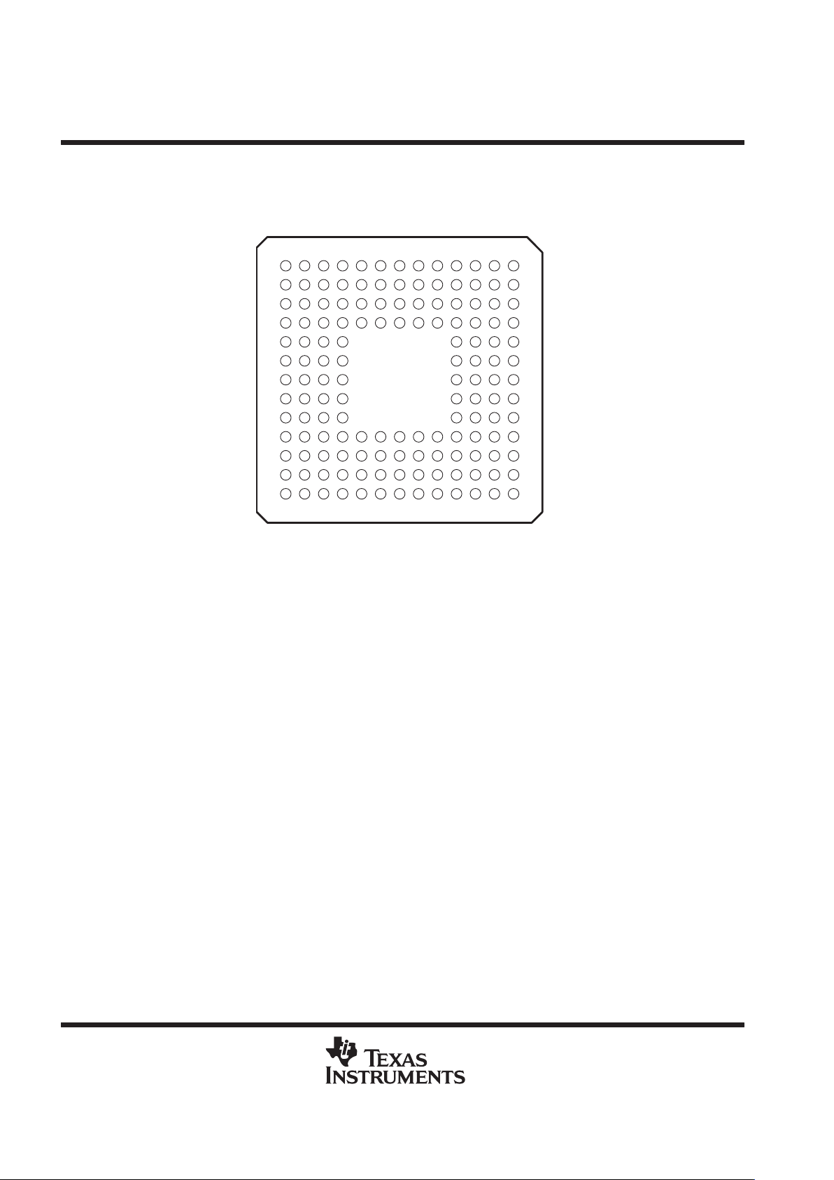
GGU PACKAGE
(BOTTOM VIEW)
A
B
D
C
E
F
H
J
L
M
K
N
G
12
3456781012 1113 9
The pin assignments table to follow lists each signal quadrant and BGA ball pin number for the 144-pin BGA
package.
The ’549 signal descriptions table lists each terminal name, function, and operating mode(s) for the
TMS320LC549GGU.
TMS320LC549
FIXED-POINT DIGITAL SIGNAL PROCESSOR
SPRS077B – SEPTEMBER 1998 – REVISED FEBRUARY 2000
5
POST OFFICE BOX 1443 • HOUSTON, TEXAS 77251–1443
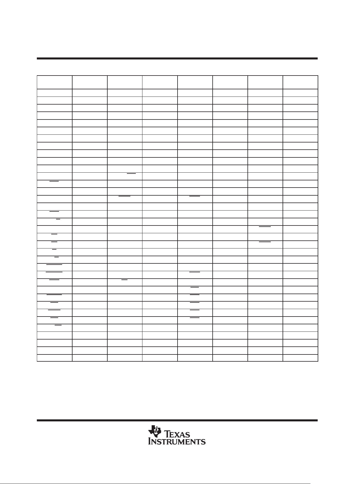
Pin Assignments for the 144-Pin BGA Package
†
SIGNAL
QUADRANT 1
BGA BALL #
SIGNAL
QUADRANT 2
BGA BALL #
SIGNAL
QUADRANT 3
BGA BALL #
SIGNAL
QUADRANT 4
BGA BALL #
V
SS
A1 BFSX1 N13 V
SS
N1 A19 A13
A22 B1 BDX1 M13 BCLKR1 N2 A20 A12
V
SS
C2 DV
DD
L12 HCNTL0 M3 V
SS
B11
DV
DD
C1 V
SS
L13 V
SS
N3 DV
DD
A11
A10 D4 CLKMD1 K10 BCLKR0 K4 D6 D10
HD7 D3 CLKMD2 K11 TCLKR L4 D7 C10
A11 D2 CLKMD3 K12 BFSR0 M4 D8 B10
A12 D1 TEST1 K13 TFSR/TADD N4 D9 A10
A13 E4 HD2 J10 BDR0 K5 D10 D9
A14 E3 TOUT J11 HCNTL1 L5 D11 C9
A15 E2 EMU0 J12 TDR M5 D12 B9
CV
DD
E1 EMU1/OFF J13 BCLKX0 N5 HD4 A9
HAS F4 TDO H10 TCLKX K6 D13 D8
V
SS
F3 TDI H11 V
SS
L6 D14 C8
V
SS
F2 TRST H12 HINT M6 D15 B8
CV
DD
F1 TCK H13 CVDD N6 HD5 A8
HCS G2 TMS G12 BFSX0 M7 CV
DD
B7
HR/W G1 V
SS
G13 TFSX/TFRM N7 V
SS
A7
READY G3 CV
DD
G11 HRDY L7 HDS1 C7
PS G4 HPIENA G10 DV
DD
K7 V
SS
D7
DS H1 V
SS
F13 V
SS
N8 HDS2 A6
IS H2 CLKOUT F12 HD0 M8 DV
DD
B6
R/W H3 HD3 F11 BDX0 L8 A0 C6
MSTRB H4 X1 F10 TDX K8 A1 D6
IOSTRB J1 X2/CLKIN E13 IACK N9 A2 A5
MSC J2 RS E12 HBIL M9 A3 B5
XF J3 D0 E11 NMI L9 HD6 C5
HOLDA J4 D1 E10 INT0 K9 A4 D5
IAQ K1 D2 D13 INT1 N10 A5 A4
HOLD K2 D3 D12 INT2 M10 A6 B4
BIO K3 D4 D11 INT3 L10 A7 C4
MP/MC L1 D5 C13 CV
DD
N11 A8 A3
DV
DD
L2 A16 C12 HD1 M11 A9 B3
V
SS
L3 V
SS
C11 V
SS
L11 CV
DD
C3
BDR1 M1 A17 B13 BCLKX1 N12 A21 A2
BFSR1 M2 A18 B12 V
SS
M12 V
SS
B2
†
DVDD is the power supply for the I/O pins while CVDD is the power supply for the core CPU, and VSS is the ground for both the I/O pins and the
core CPU.

TMS320LC549
FIXED-POINT DIGITAL SIGNAL PROCESSOR
SPRS077B – SEPTEMBER 1998 – REVISED FEBRUARY 2000
6
POST OFFICE BOX 1443 • HOUSTON, TEXAS 77251–1443
Signal Descriptions
TERMINAL
NAME TYPE
†
DESCRIPTION
DATA SIGNALS
A22 (MSB)
A21
A20
A19
A18
A17
A16
A15
A14
A13
A12
A11
A10
A9
A8
A7
A6
A5
A4
A3
A2
A1
A0 (LSB)
O/Z
Parallel port address bus A22 (MSB) through A0 (LSB). The sixteen LSBs (A15–A0) are multiplexed to address
external data/program memory or I/O. A15–A0 are placed in the high-impedance state in the hold mode. A15–A0
also go into the high-impedance state when EMU1/OFF
is low. The seven MSBs (A22 to A16) are used for
extended program memory addressing.
The address bus have a feature called bus holder that eliminates passive components and the power dissipation
associated with it. The bus holders keep the address bus at the previous logic level when the bus goes into a
high-impedance state. The bus holders on the address bus are always enabled.
D15 (MSB)
D14
D13
D12
D11
D10
D9
D8
D7
D6
D5
D4
D3
D2
D1
D0 (LSB)
I/O/Z
Parallel port data bus D15 (MSB) through D0 (LSB). D15–D0 are multiplexed to transfer data between the core
CPU and external data/program memory or I/O devices. D15–D0 are placed in the high-impedance state when
not output or when RS
or HOLD is asserted. D15–D0 also go into the high-impedance state when EMU1/OFF
is low.
The data bus has a feature called bus holder that eliminates passive components and the power dissipation
associated with it. The bus holders keep the data bus at the previous logic level when the bus goes into a
high-impedance state. These bus holders are enabled or disabled by the BH bit in the bank switching control
register (BSCR).
INITIALIZATION, INTERRUPT AND RESET OPERATIONS
IACK O/Z
Interrupt acknowledge signal. IACK indicates the receipt of an interrupt and that the program counter is fetching
the interrupt vector location designated by A15–0. IACK
also goes into the high-impedance state when
EMU1/OFF
is low.
INT0
INT1
INT2
INT3
I
External user interrupt inputs. INT0–INT3 are prioritized and are maskable by the interrupt mask register and the
interrupt mode bit. INT0
–INT3 can be polled and reset by the interrupt flag register.
†
I = Input, O = Output, Z = High impedance
TMS320LC549
FIXED-POINT DIGITAL SIGNAL PROCESSOR
SPRS077B – SEPTEMBER 1998 – REVISED FEBRUARY 2000
7
POST OFFICE BOX 1443 • HOUSTON, TEXAS 77251–1443
Signal Descriptions (Continued)
TERMINAL
DESCRIPTION
NAME
DESCRIPTION
TYPE
†
INITIALIZATION, INTERRUPT AND RESET OPERATIONS (CONTINUED)
NMI I
Nonmaskable interrupt. NMI is an external interrupt that cannot be masked by way of the INTM or the IMR. When
NMI
is activated, the processor traps to the appropriate vector location.
RS I
Reset input. RS causes the DSP to terminate execution and forces the program counter to 0FF80h. When RS
is brought to a high level, execution begins at location 0FF80h of the program memory. RS affects various
registers and status bits.
MP/MC I
Microprocessor/microcomputer mode-select pin. If active-low at reset (microcomputer mode), MP/MC causes
the internal program ROM to be mapped into the upper program memory space. In the microprocessor mode,
off-chip memory and its corresponding addresses (instead of internal program ROM) are accessed by the DSP.
CNT I
I/O level select. For 5-V operation, all input and output voltage levels are TTL-compatible when CNT is pulled
down to a low level. For 3-V operation with CMOS-compatible I/O interface levels, CNT is pulled to a high level.
MULTIPROCESSING SIGNALS
BIO I
Branch control input. A branch can be conditionally executed when BIO is active. If low, the processor executes
the conditional instruction. The BIO
condition is sampled during the decode phase of the pipeline for the XC
instruction, and all other instructions sample BIO
during the read phase of the pipeline.
XF O/Z
External flag output (latched software-programmable signal). XF is set high by the SSBX XF instruction, set low
by RSBX XF instruction or by loading the ST1 status register. XF is used for signaling other processors in
multiprocessor configurations or as a general-purpose output pin. XF goes into the high-impedance state when
OFF
is low, and is set high at reset.
MEMORY CONTROL SIGNALS
DS
PS
IS
O/Z
Data, program, and I/O space select signals. DS, PS, and IS are always high unless driven low for communicating
to a particular external space. Active period corresponds to valid address information. Placed into a
high-impedance state in hold mode. DS
, PS, and IS also go into the high-impedance state when EMU1/OFF is
low.
MSTRB O/Z
Memory strobe signal. MSTRB is always high unless low-level asserted to indicate an external bus access to data
or program memory. Placed in high-impedance state in hold mode. MSTRB
also goes into the high-impedance
state when OFF
is low.
READY I
Data-ready input. READY indicates that an external device is prepared for a bus transaction to be completed.
If the device is not ready (READY is low), the processor waits one cycle and checks READY again. Note that the
processor performs ready-detection if at least two software wait states are programmed. The READY signal is
not sampled until the completion of the software wait states.
R/W O/Z
Read/write signal. R/W indicates transfer direction during communication to an external device and is normally
high (in read mode), unless asserted low when the DSP performs a write operation. Placed in the high-impedance
state in hold mode, R/W
also goes into the high-impedance state when EMU1/OFF is low.
IOSTRB O/Z
I/O strobe signal. IOSTRB is always high unless low level asserted to indicate an external bus access to an I/O
device. Placed in high-impedance state in hold mode. IOSTRB
also goes into the high-impedance state when
EMU1/OFF
is low.
HOLD I
Hold input. HOLD is asserted to request control of the address, data, and control lines. When acknowledged by
the ’54x, these lines go into high-impedance state.
HOLDA O/Z
Hold acknowledge signal. HOLDA indicates to the external circuitry that the processor is in a hold state and that
the address, data, and control lines are in a high-impedance state, allowing them to be available to the external
circuitry. HOLDA
also goes into the high-impedance state when EMU1/OFF is low.
MSC O/Z
Microstate complete signal. Goes low on CLKOUT falling at the start of the first software wait state. Remains low
until one CLKOUT cycle before the last programmed software wait state. If connected to the READY line, MSC
forces one external wait state after the last internal wait state has been completed. MSC also goes into the
high-impedance state when EM1/OFF
is low.
†
I = Input, O = Output, Z = High impedance
TMS320LC549
FIXED-POINT DIGITAL SIGNAL PROCESSOR
SPRS077B – SEPTEMBER 1998 – REVISED FEBRUARY 2000
8
POST OFFICE BOX 1443 • HOUSTON, TEXAS 77251–1443
Signal Descriptions (Continued)
TERMINAL
DESCRIPTION
NAME
DESCRIPTION
TYPE
†
MEMORY CONTROL SIGNALS (CONTINUED)
IAQ O/Z
Instruction acquisition signal. IAQ is asserted (active low) when there is an instruction address on the address
bus and goes into the high-impedance state when EMU1/OFF
is low.
OSCILLATOR/TIMER SIGNALS
CLKOUT O/Z
Master clock output signal. CLKOUT cycles at the machine-cycle rate of the CPU. The internal machine cycle
is bounded by the falling edges of this signal. CLKOUT also goes into the high-impedance state when EMU1/OFF
is low.
CLKMD1
CLKMD2
CLKMD3
I
Clock mode external/internal input signals. CLKMD1, CLKMD2, and CLKMD3 allow you to select and configure
different clock modes, such as crystal, external clock, and various PLL factors. Refer to PLL section for a detailed
functional description of these pins.
X2/CLKIN I
Input pin to internal oscillator from the crystal. If the internal (crystal) oscillator is not being used, a clock can
become input to the device using this pin. The internal machine cycle time is determined by the clock
operating-mode pins (CLKMD1, CLKMD2 and CLKMD3).
X1 O
Output pin from the internal oscillator for the crystal. If the internal oscillator is not used, X1 should be left
unconnected. X1 does not go into the high-impedance state when EMU1/OFF
is low.
TOUT O/Z
Timer output. TOUT signals a pulse when the on-chip timer counts down past zero. The pulse is a CLKOUT -cycle
wide. TOUT also goes into the high-impedance state when EMU1/OFF
is low.
BUFFERED SERIAL PORT 0 AND BUFFERED SERIAL PORT 1 SIGNALS
BCLKR0
BCLKR1
I
Receive clocks. External clock signal for clocking data from the data-receive (DR) pin into the buffered serial port
receive shift registers (RSRs). Must be present during buffered serial port transfers. If the buffered serial port is
not being used, BCLKR0 and BCLKR1 can be sampled as an input by way of IN0 bit of the SPC register.
BCLKX0
BCLKX1
I/O/Z
Transmit clock. Clock signal for clocking data from the serial port transmit shift register (XSR) to the data transmit
(DX) pin. BCLKX can be an input if MCM in the serial port control register is cleared to 0. It also can be driven
by the device at 1/(CLKDV + 1) where CLKDV range is 0–31 CLKOUT frequency when MCM is set to 1. If the
buffered serial port is not used, BCLKX can be sampled as an input by way of IN1 of the SPC register . BCLKX0
and BCLKX1 go into the high-impedance state when OFF
is low.
BDR0
BDR1
I Buffered serial-data-receive input. Serial data is received in the RSR by BDR0/BDR1.
BDX0
BDX1
O/Z
Buffered serial-port-transmit output. Serial data is transmitted from the XSR by way of BDX. BDX0 and BDX1 are
placed in the high-impedance state when not transmitting and when EMU1/OFF
is low.
BFSR0
BFSR1
I
Frame synchronization pulse for receive input. The falling edge of the BFSR pulse initiates the data-receive
process, beginning the clocking of the RSR.
BFSX0
BFSX1
I/O/Z
Frame synchronization pulse for transmit input/output. The falling edge of the BFSX pulse initiates the
data-transmit process, beginning the clocking of the XSR. Following reset, the default operating condition of
BFSX is an input. BFSX0 and BFSX1 can be selected by software to be an output when TXM in the serial control
register is set to 1. This pin goes into the high-impedance state when EMU1/OFF
is low.
SERIAL PORT 0 AND SERIAL PORT 1 SIGNALS
CLKR0
CLKR1
I
Receive clocks. External clock signal for clocking data from the data receive (DR) pin into the serial port receive
shift register (RSR). Must be present during serial port transfers. If the serial port is not being used, CLKR0 and
CLKR1 can be sampled as an input via IN0 bit of the SPC register.
CLKX0
CLKX1
I/O/Z
Transmit clock. Clock signal for clocking data from the serial port transmit shift register (XSR) to the data transmit
(DX) pin. CLKX can be an input if MCM in the serial port control register is cleared to 0. It also can be driven by
the device at 1/4 CLKOUT frequency when MCM is set to 1. If the serial port is not used, CLKX can be sampled
as an input via IN1 of the SPC register. CLKX0 and CLKX1 go into the high-impedance state when EMU1/OFF
is low.
DR0
DR1
I
Serial-data-receive input. Serial data is received in the RSR by DR.
†
I = Input, O = Output, Z = High impedance
TMS320LC549
FIXED-POINT DIGITAL SIGNAL PROCESSOR
SPRS077B – SEPTEMBER 1998 – REVISED FEBRUARY 2000
9
POST OFFICE BOX 1443 • HOUSTON, TEXAS 77251–1443
Signal Descriptions (Continued)
TERMINAL
DESCRIPTION
NAME
DESCRIPTION
TYPE
†
SERIAL PORT 0 AND SERIAL PORT 1 SIGNALS (CONTINUED)
DX0
DX1
O/Z
Serial port transmit output. Serial data is transmitted from the XSR via DX. DX0 and DX1 are placed in the
high-impedance state when not transmitting and when EMU1/OFF
is low.
FSR0
FSR1
I
Frame synchronization pulse for receive input. The falling edge of the FSR pulse initiates the data-receive
process, beginning the clocking of the RSR.
FSX0
FSX1
I/O/Z
Frame synchronization pulse for transmit input/output. The falling edge of the FSX pulse initiates the data transmit
process, beginning the clocking of the XSR. Following reset, the default operating condition of FSX is an input.
FSX0 and FSX1 can be selected by software to be an output when TXM in the serial control register is set to 1.
This pin goes into the high-impedance state when EMU1/OFF is low.
TDM SERIAL PORT SIGNALS
TCLKR I TDM receive clock input
TDR I TDM serial data-receive input
TFSR/TADD I/O TDM receive frame synchronization or TDM address
TCLKX I/O/Z TDM transmit clock
TDX O/Z TDM serial data-transmit output
TFSX/TFRM I/O/Z TDM transmit frame synchronization
HOST-PORT INTERFACE SIGNALS
HD0–HD7 I/O/Z
Parallel bidirectional data bus. HD0–HD7 are placed in the high-impedance state when not outputting data. The
signals go into the high-impedance state when EMU1/OFF
is low. These pins each have bus holders similar to
those on the address/data bus, but which are always enabled.
HCNTL0
HCNTL1
I Control inputs
HBIL I Byte-identification input
HCS I Chip-select input
HDS1
HDS2
I Data strobe inputs
HAS I Address strobe input
HR/W I Read/write input
HRDY O/Z Ready output. This signal goes into the high-impedance state when EMU1/OFF is low.
HINT O/Z
Interrupt output. When the DSP is in reset, this signal is driven high. The signal goes into the high-impedance
state when EMU1/OFF
is low.
HPIENA I
HPI module select input. This signal must be tied to a logic 1 state to have HPI selected. If this input is left open
or connected to ground, the HPI module will not be selected, internal pullup for the HPI input pins are enabled,
and the HPI data bus has keepers set. This input is provided with an internal pull-down resistor which is active
only when RS
is low. HPIENA is sampled when RS goes high and ignored until RS goes low again. Refer to the
Electrical Characteristics section for the input current requirements for this pin.
SUPPLY PINS
CV
DD
Supply +VDD. CVDD is the dedicated power supply for the core CPU.
DV
DD
Supply +VDD. DVDD is the dedicated power supply for I/O pins.
V
SS
Supply Ground. VSS is the dedicated power ground for the device.
†
I = Input, O = Output, Z = High impedance
TMS320LC549
FIXED-POINT DIGITAL SIGNAL PROCESSOR
SPRS077B – SEPTEMBER 1998 – REVISED FEBRUARY 2000
10
POST OFFICE BOX 1443 • HOUSTON, TEXAS 77251–1443
Signal Descriptions (Continued)
TERMINAL
DESCRIPTION
NAME
DESCRIPTION
TYPE
†
IEEE1149.1 TEST PINS
TCK I
IEEE standard 1149.1 test clock. Pin with internal pullup device. This is normally a free-running clock signal with
a 50% duty cycle. The changes on the test-access port (TAP) of input signals TMS and TDI are clocked into the
TAP controller, instruction register , or selected test data register on the rising edge of TCK. Changes at the T AP
output signal (TDO) occur on the falling edge of TCK.
TDI I
IEEE standard 1149.1 test data input. Pin with internal pullup device. TDI is clocked into the selected register
(instruction or data) on a rising edge of TCK.
TDO O/Z
IEEE standard 1149.1 test data output. The contents of the selected register (instruction or data) is shifted out
of TDO on the falling edge of TCK. TDO is in the high-impedance state except when the scanning of data is in
progress. TDO also goes into the high-impedance state when EMU1/OFF
is low.
TMS I
IEEE standard 1149.1 test mode select. Pin with internal pullup device. This serial control input is clocked into
the TAP controller on the rising edge of TCK.
TRST I
IEEE standard 1149.1 test reset. TRST, when high, gives the IEEE standard 1149.1 scan system control of the
operations of the device. If TRST
is not connected or driven low, the device operates in its functional mode, and
the IEEE standard 1149.1 signals are ignored. Pin with internal pulldown device.
EMU0 I/O/Z
Emulator interrupt 0 pin. When TRST is driven low, EMU0 must be high for the activation of the EMU1/OFF
condition. When TRST is driven high, EMU0 is used as an interrupt to or from the emulator system and is defined
as input/output by way of IEEE standard 1149.1 scan system.
EMU1/OFF I/O/Z
Emulator interrupt 1 pin/disable all outputs. When TRST is driven high, EMU1/OFF is used as an interrupt to or
from the emulator system and is defined as input/output by way of IEEE standard 1149.1 scan system. When
TRST
is driven low, EMU1/OFF is configured as OFF. The EMU1/OFF signal, when active low, puts all output
drivers into the high-impedance state. Note that OFF
is used exclusively for testing and emulation purposes (not
for multiprocessing applications). Therefore, for the OFF
condition, the following conditions apply:
TRST
= low,
EMU0 = high
EMU1/OFF
= low
DEVICE TEST PIN
TEST1 I Test1 – Reserved for internal use only. This pin must not be connected (NC).
†
I = Input, O = Output, Z = High impedance
TMS320LC549
FIXED-POINT DIGITAL SIGNAL PROCESSOR
SPRS077B – SEPTEMBER 1998 – REVISED FEBRUARY 2000
11
POST OFFICE BOX 1443 • HOUSTON, TEXAS 77251–1443
absolute maximum ratings over specified temperature range (unless otherwise noted)
†
Supply voltage, DVDD‡ –0.3 V to 4.6 V. . . . . . . . . . . . . . . . . . . . . . . . . . . . . . . . . . . . . . . . . . . . . . . . . . . . . . . . . . . .
Input voltage range –0.3 V to 4.6 V. . . . . . . . . . . . . . . . . . . . . . . . . . . . . . . . . . . . . . . . . . . . . . . . . . . . . . . . . . . . . . . .
Output voltage range –0.3 V to 4.6 V. . . . . . . . . . . . . . . . . . . . . . . . . . . . . . . . . . . . . . . . . . . . . . . . . . . . . . . . . . . . . .
Operating case temperature range, T
C
–40°C to 100°C. . . . . . . . . . . . . . . . . . . . . . . . . . . . . . . . . . . . . . . . . . . . . .
Storage temperature range, T
stg
–55°C to 150°C. . . . . . . . . . . . . . . . . . . . . . . . . . . . . . . . . . . . . . . . . . . . . . . . . . . .
†
Stresses beyond those listed under “absolute maximum ratings” may cause permanent damage to the device. These are stress ratings only, and
functional operation of the device at these or any other conditions beyond those indicated under “recommended operating conditions” is not
implied. Exposure to absolute-maximum-rated conditions for extended periods may affect device reliability.
‡
All voltage values are with respect to VSS.
recommended operating conditions
MIN NOM MAX UNIT
DV
DD
Device supply voltage 3 3.3 3.6 V
V
SS
Supply voltage, GND 0 V
V
High-level input voltage
Schmitt trigger inputs, DVDD =
3.3"0.3 V
§
2.5 DVDD + 0.3
V
VIHHigh level in ut voltage
All other inputs 2 DVDD + 0.3
V
V
IL
Low-level input voltage –0.3 0.8 V
I
OH
High-level output current –300 µA
I
OL
Low-level output current 1.5 mA
T
C
Operating case temperature –40 100 °C
§
The following pins have schmitt trigger inputs: RS
, INTn, NMI, X2/CLKIN, CLKMDn, TCK, HAS, HCS, HDSn, BCLKRn, TCLKR, BCLKXn, and
TCLKX
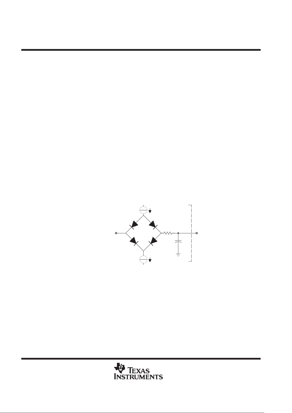
Refer to Figure 1 for 3.3-V device test load circuit values.
TMS320LC549
FIXED-POINT DIGITAL SIGNAL PROCESSOR
SPRS077B – SEPTEMBER 1998 – REVISED FEBRUARY 2000
12
POST OFFICE BOX 1443 • HOUSTON, TEXAS 77251–1443
PARAMETER MEASUREMENT INFORMATION
timing parameter symbology
Timing parameter symbols used are created in accordance with JEDEC Standard 100-A. To shorten the
symbols, some of the pin names and other related terminology have been abbreviated as follows:
Lowercase subscripts and their meanings: Letters and symbols and their meanings:
a access time H High
c cycle time (period) L Low
d delay time V Valid
dis disable time Z High impedance
en enable time
f fall time
h hold time
r rise time
su setup time
t transition time
v valid time
w pulse duration (width)
X Unknown, changing, or don’t care level
signal transition reference points
All timing references are made at a voltage of 1.5 volts, except rise and fall times which are referenced at the
10% and 90% points of the specified low and high logic levels, respectively.
Tester Pin
Electronics
V
Load
I
OL
C
T
I
OH
Output
Under
Test
50 Ω
Where: I
OL
= 1.5 mA (all outputs)
I
OH
= 300 µA (all outputs)
V
Load
= 1.5 V
C
T
= 40 pF typical load circuit capacitance.
Figure 1. 3.3-V Test Load Circuit
TMS320LC549
FIXED-POINT DIGITAL SIGNAL PROCESSOR
SPRS077B – SEPTEMBER 1998 – REVISED FEBRUARY 2000
13
POST OFFICE BOX 1443 • HOUSTON, TEXAS 77251–1443
electrical characteristics and operating conditions
electrical characteristics over recommended operating case temperature range (unless otherwise
noted)
PARAMETER TEST CONDITIONS MIN TYP†MAX UNIT
V
OH
High-level output voltage
‡
VDD = 3.3"0.3 V , IOH = MAX 2.4 V
V
OL
Low-level output voltage
‡
IOL = MAX 0.4 V
Input current in high
A[22:0] VDD = MAXk –150 250
I
IZ
In ut current in high
impedance
All other pins
VDD = MAX, VI = VSS to V
DD
–10 10
µA
TRST With internal pulldown –10 800
p
HPIENA With internal pulldown, RS = 0 –10 400
Input current
(
V
= V
to V
)
TMS, TCK, TDI, HPI||With internal pullups –400 10
I
I
(V
I
=
V
SS
to
VDD)
Input current
D[15:0], HD[7:0]
Bus holders enabled, VDD = MAXk –150 250
µA
(VI = VSS to VDD)
X2/CLKIN
Oscillator enabled – 40 40
All other input-only pins –10 10
I
DDC
Supply current, core CPU VDD = 3.3 V, fx = 40 MHz,§ TC = 25°C 28
¶
mA
I
DDP
Supply current, pins DVDD = 3.3 V, fx = 40 MHz,§ TC = 25°C 10.8
#
mA
Supply current,
IDLE2 PLL × 1 mode, 40 MHz input 2 mA
I
DD
Su ly current,
standby
IDLE3
Divide-by-two mode, CLKIN stopped 15 µA
C
i
Input capacitance 10 pF
C
o
Output capacitance 10 pF
†
All values are typical unless otherwise specified.
‡
All input and output voltage levels except RS
, INT0–INT3, NMI, CNT, X2/CLKIN, CLKMD0–CLKMD3 are LVTTL-compatible.
§
Clock mode: PLL × 1 with external source
¶
This value was obtained with 50% usage of MAC and 50% usage of NOP instructions. Actual operating current varies with program being
executed.
#
This value was obtained with single-cycle external writes, CLKOFF = 0 and load = 15 pF . For more details on how this calculation is performed,
refer to the
Calculation of TMS320C54x Power Dissipation
application report (literature number SPRA164).
||
HPI input signals except for HPIENA.
kV
IL(MIN)
≤ VI ≤ V
IL(MAX)
or V
IH(MIN)
≤ VI≤ V
IH(MAX)
TMS320LC549
FIXED-POINT DIGITAL SIGNAL PROCESSOR
SPRS077B – SEPTEMBER 1998 – REVISED FEBRUARY 2000
14
POST OFFICE BOX 1443 • HOUSTON, TEXAS 77251–1443
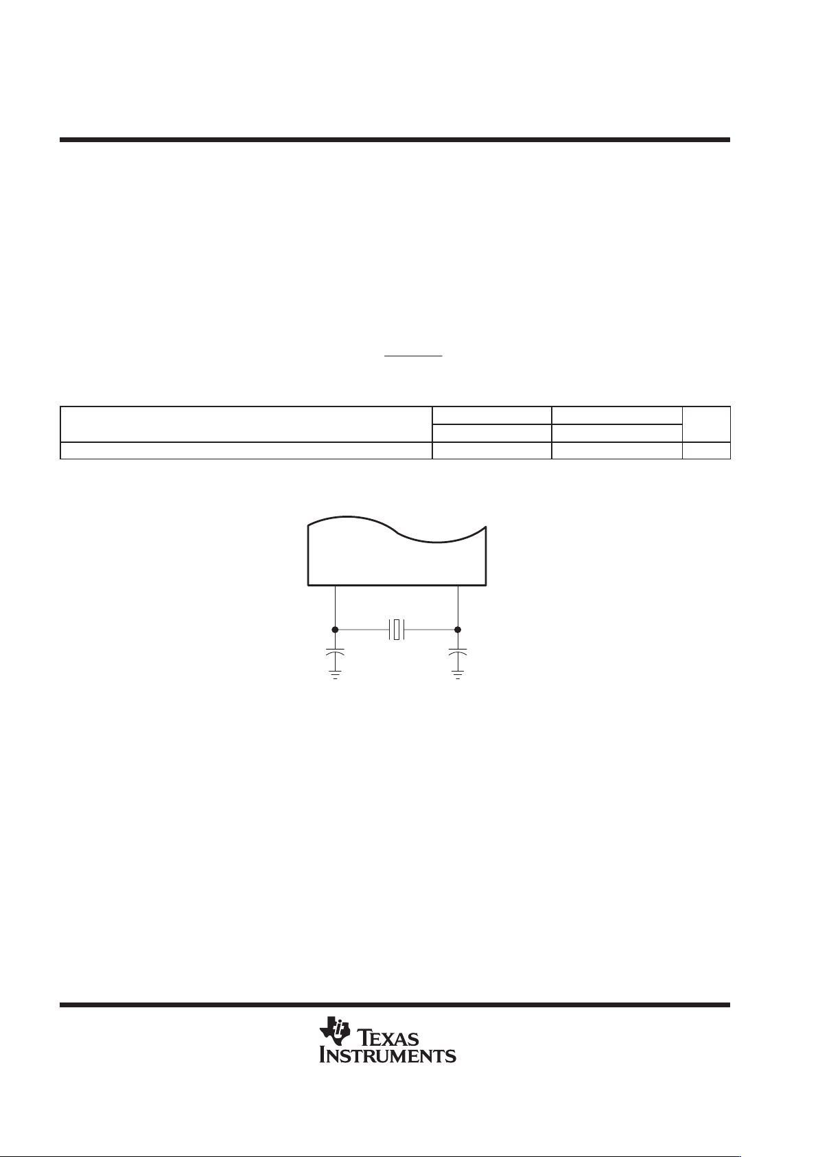
internal oscillator with external crystal
The internal oscillator is enabled by selecting the appropriate clock mode at reset (this is device-dependent –
see PLL section) and connecting a crystal or ceramic resonator across X1 and X2/CLKIN. The CPU clock
frequency is one-half the crystal’s oscillation frequency following reset. After reset, the clock mode of the devices
with the software PLL can also be changed to divide-by-four. Since the internal oscillator can be used as a clock
source to the PLL, the crystal oscillation frequency can be multiplied to generate the CPU clock if desired.
The crystal should be in fundamental mode operation and parallel resonant with an effective series resistance
of 30ohms and power dissipation of 1 mW. The connection of the required circuit, consisting of the crystal and
two load capacitors, is shown in Figure 2. The load capacitors, C
1
and C2, should be chosen such that the
equation below is satisfied. CL in the equation is the load specified for the crystal.
C
L
+
C1C
2
(
C
1
)
C
2
)
recommended operating conditions (see Figure 2)
’549-66 ’549-80
MIN NOM MAX MIN NOM MAX
UNIT
f
x
Input clock frequency 10
†
20
‡
10
†
20
‡
MHz
†
This device utilizes a fully static design and therefore can operate with t
c(CI)
approaching ∞. The device is characterized at frequencies
approaching 0 Hz.
‡
It is recommended that the PLL clocking option be used for maximum frequency operation.
X1 X2/CLKIN
C1 C2
Crystal
Figure 2. Internal Divide-by-Two Clock Option With External Crystal
TMS320LC549
FIXED-POINT DIGITAL SIGNAL PROCESSOR
SPRS077B – SEPTEMBER 1998 – REVISED FEBRUARY 2000
15
POST OFFICE BOX 1443 • HOUSTON, TEXAS 77251–1443
divide-by-two/divide-by-four clock option – PLL disabled
The frequency of the reference clock provided at the X2/CLKIN pin can be divided by a factor of two or four to
generate the internal machine cycle. The selection of the clock mode is described in the clock generator section.
When an external clock source is used, the frequency injected must conform to specifications listed in the timing
requirements table.
switching characteristics over recommended operating conditions [H = 0.5t
c(CO)
] (see Figure 2 and
Figure 3, and the recommended operating conditions table)
’549-66 ’549-80
PARAMETER
MIN TYP MAX MIN TYP MAX
UNIT
t
c(CO)
Cycle time, CLKOUT 15‡2t
c(CI)
†
12.5‡2t
c(CI)
†
ns
t
d(CIH-CO)
Delay time, X2/CLKIN high to CLKOUT high/low 3 6 10 3 6 10 ns
t
f(CO)
Fall time, CLKOUT
†
2 2 ns
t
r(CO)
Rise time, CLKOUT
†
2 2 ns
t
w(COL)
Pulse duration, CLKOUT low
†
H–4 H–2 H H–3 H–1 H ns
t
w(COH)
Pulse duration, CLKOUT high
†
H–4 H–2 H H–3 H–1 H ns
†
This device utilizes a fully static design and therefore can operate with t
c(CI)
approaching ∞. The device is characterized at frequencies
approaching 0 Hz.
‡
It is recommended that the PLL clocking option be used for maximum frequency operation.
TMS320LC549
FIXED-POINT DIGITAL SIGNAL PROCESSOR
SPRS077B – SEPTEMBER 1998 – REVISED FEBRUARY 2000
16
POST OFFICE BOX 1443 • HOUSTON, TEXAS 77251–1443
divide-by-two/divide-by-four clock option – PLL disabled (continued)
timing requirements (see Figure 3)
’549-66 ’549-80
MIN MAX MIN MAX
UNIT
t
c(CI)
Cycle time, X2/CLKIN 20
‡
†
20
‡
†
ns
t
f(CI)
Fall time, X2/CLKIN 8 8 ns
t
r(CI)
Rise time, X2/CLKIN 8 8 ns
t
w(CIL)
Pulse duration, X2/CLKIN low 5
†
5
†
ns
t
w(CIH)
Pulse duration, X2/CLKIN high 5
†
5
†
ns
†
This device utilizes a fully static design and therefore can operate with t
c(CI)
approaching ∞. The device is characterized at frequencies
approaching 0 Hz.
‡
It is recommended that the PLL clocking option be used for maximum frequency operation.
t
r(CO)
t
f(CO)
CLKOUT
X2/CLKIN
t
w(COL)
t
d(CIH-CO)
t
f(CI)
t
r(CI)
t
c(CO)
t
c(CI)
t
w(COH)
t
w(CIL)
t
w(CIH)
Figure 3. External Divide-by-Two Clock Timing
TMS320LC549
FIXED-POINT DIGITAL SIGNAL PROCESSOR
SPRS077B – SEPTEMBER 1998 – REVISED FEBRUARY 2000
17
POST OFFICE BOX 1443 • HOUSTON, TEXAS 77251–1443
multiply-by-N clock option – PLL enabled
The frequency of the reference clock provided at the X2/CLKIN pin can be multiplied by a factor of N to generate
the internal machine cycle. The selection of the clock mode and the value of N is described in the clock generator
section.
When an external clock source is used, the frequency injected must conform to specifications listed in the timing
requirements table.
switching characteristics over recommended operating conditions [H = 0.5t
c(CO)
] (see Figure 2 and
Figure 4, and the recommended operating conditions table)
’549-66 ’549-80
PARAMETER
MIN TYP MAX MIN TYP MAX
UNIT
t
c(CO)
Cycle time, CLKOUT 15 t
c(CI)/N
12.5 t
c(CI)/N
ns
t
d(CIH-CO)
Delay time, X2/CLKIN high/low to CLKOUT high/low 3 6 10 3 6 10 ns
t
f(CO)
Fall time, CLKOUT 2 2 ns
t
r(CO)
Rise time, CLKOUT 2 2 ns
t
w(COL)
Pulse duration, CLKOUT low H–4 H–2 H H–3 H–1 H ns
t
w(COH)
Pulse duration, CLKOUT high H–4 H–2 H H–3 H–1 H ns
t
p
Transitory phase, PLL lock-up time 50 29
ms
TMS320LC549
FIXED-POINT DIGITAL SIGNAL PROCESSOR
SPRS077B – SEPTEMBER 1998 – REVISED FEBRUARY 2000
18
POST OFFICE BOX 1443 • HOUSTON, TEXAS 77251–1443
multiply-by-N clock option – PLL enabled (continued)
timing requirements (see Figure 4)
’549-66 ’549-80
MIN MAX MIN MAX
UNIT
Integer PLL multiplier N (N = 1–15) 20
†
200 20†200
t
Cycle time, X2/CLKIN
PLL multiplier N = x.5
20
†
100 20†100
ns
t
c(CI)
Cycle time, X2/CLKIN
PLL multiplier N = x.25, x.75
20
†
50 20
†
50
ns
t
f(CI)
Fall time, X2/CLKIN 8 8 ns
t
r(CI)
Rise time, X2/CLKIN 8 8 ns
t
w(CIL)
Pulse duration, X2/CLKIN low 5 5 ns
t
w(CIH)
Pulse duration, X2/CLKIN high 5 5 ns
†
Note that for all values of t
c(CI)
, the minimum t
c(CO)
period must not be exceeded.
t
c(CO)
t
c(CI)
t
w(COH)
t
f(CO)
t
r(CO)
t
f(CI)
X2/CLKIN
CLKOUT
t
d(CIH-CO)
t
w(COL)
t
r(CI)
tp
Unstable
t
w(CIH)
t
w(CIL)
Figure 4. External Multiply-by-One Clock Timing
TMS320LC549
FIXED-POINT DIGITAL SIGNAL PROCESSOR
SPRS077B – SEPTEMBER 1998 – REVISED FEBRUARY 2000
19
POST OFFICE BOX 1443 • HOUSTON, TEXAS 77251–1443
memory and parallel I/O interface timing
switching characteristics over recommended operating conditions for a memory read
(MSTRB
= 0)†‡ (see Figure 5)
’549-66 ’549-80
PARAMETER
MIN MAX MIN MAX
UNIT
t
d(CLKL-A)
Delay time, address valid from CLKOUT low
§
– 1 6 – 1 6 ns
t
d(CLKH-A)
Delay time, address valid from CLKOUT high (transition)
¶
– 1 5 – 1 5 ns
t
d(CLKL-MSL)
Delay time, MSTRB low from CL KOUT low – 1 5 – 1 5 ns
t
d(CLKL-MSH)
Delay time, MSTRB high from CLKOUT low – 1 6 – 1 6 ns
t
h(CLKL-A)R
Hold time, address valid after CLKOUT low
§
– 1 6 – 1 6 ns
t
h(CLKH-A)R
Hold time, address valid after CLKOUT high
¶
– 1 5 – 1 5 ns
†
Address, PS, and DS timings are all included in timings referenced as address.
‡
See Table 1, Table 2, and Table 3 for address bus timing variation with load capacitance.
§
In the case of a memory read preceded by a memory read
¶
In the case of a memory read preceded by a memory write

TMS320LC549
FIXED-POINT DIGITAL SIGNAL PROCESSOR
SPRS077B – SEPTEMBER 1998 – REVISED FEBRUARY 2000
20
POST OFFICE BOX 1443 • HOUSTON, TEXAS 77251–1443
memory and parallel I/O interface timing (continued)
timing requirements for a memory read (MSTRB = 0) [H = 0.5 t
c(CO)
]†‡ (see Figure 5)
’549-66 ’549-80
MIN MAX MIN MAX
UNIT
t
a(A)M
Access time, read data access from address valid 2H–10 2H–10 ns
t
a(MSTRBL)
Access time, read data access from MSTRB low 2H–10 2H–10 ns
t
su(D)R
Setup time, read data before CLKOUT low 5 5 ns
t
h(D)R
Hold time, read data after CLKOUT low 0 0 ns
t
h(A-D)R
Hold time, read data after address invalid 0 0 ns
t
h(D)MSTRBH
Hold time, read data after MSTRB high 0 0 ns
†
Address, PS
, and DS timings are all included in timings referenced as address.
‡
See Table 1, Table 2, and Table 3 for address bus timing variation with load capacitance.

TMS320LC549
FIXED-POINT DIGITAL SIGNAL PROCESSOR
SPRS077B – SEPTEMBER 1998 – REVISED FEBRUARY 2000
21
POST OFFICE BOX 1443 • HOUSTON, TEXAS 77251–1443
memory and parallel I/O interface timing (continued)
PS, DS
R/W
MSTRB
D[15:0]
A[15:0]
CLKOUT
t
h(D)R
t
h(CLKL-A)R
t
d(CLKL-MSH)
t
d(CLKL-A)
t
d(CLKL-MSL)
t
su(D)R
t
a(A)M
t
a(MSTRBL)
t
h(A-D)R
t
h(D)MSTRBH
Figure 5. Memory Read (MSTRB = 0)

TMS320LC549
FIXED-POINT DIGITAL SIGNAL PROCESSOR
SPRS077B – SEPTEMBER 1998 – REVISED FEBRUARY 2000
22
POST OFFICE BOX 1443 • HOUSTON, TEXAS 77251–1443
memory and parallel I/O interface timing (continued)
switching characteristics over recommended operating conditions for a memory write
(MSTRB
= 0) [H = 0.5 t
c(CO)
]†‡ (see Figure 6)
’549-66 ’549-80
PARAMETER
MIN MAX MIN MAX
UNIT
t
d(CLKH-A)
Delay time, address valid from CLKOUT high
§
– 1 5 – 1 5 ns
t
d(CLKL-A)
Delay time, address valid from CLKOUT l ow
¶
– 1 6 – 1 6 ns
t
d(CLKL-MSL)
Delay time, MSTRB low from CL KOUT low – 1 5 – 1 5 ns
t
d(CLKL-D)W
Delay time, data valid from CLKOUT l o w 0 8 0 8 ns
t
d(CLKL-MSH)
Delay time, MSTRB high fr om CLKOUT lo w – 1 6 – 1 6 ns
t
d(CLKH-RWL)
Delay time, R/W low from CLKO UT high – 1 5 0 5 ns
t
d(CLKH-RWH)
Delay time, R/W high from CLKO UT high – 1 5 – 1 5 ns
t
d(RWL-MSTRBL)
Delay time, MSTRB low after R/W low H – 2 H + 3 H – 2 H + 3 ns
t
h(A)W
Hold time, address valid after CLKOUT high
§
– 1 5 – 1 5 ns
t
h(D)MSH
Hold time, write data valid after MSTRB high H–5 H+5
¶
H–4 H+4¶ns
t
w(SL)MS
Pulse duration, MSTRB low 2H–5 2H–5 ns
t
su(A)W
Setup time, address valid before MSTRB low 2H–5 2H–5 ns
t
su(D)MSH
Setup time, write data valid before MSTRB high 2H–10 2H+8
§
2H–7 2H+7
¶
ns
†
Address, PS, and DS timings are all included in timings referenced as address.
‡
See Table 1, Table 2, and Table 3 for address bus timing variation with load capacitance.
§
In the case of a memory write preceded by a memory write.
¶
In the case of a memory write preceded by an I/O cycle.

TMS320LC549
FIXED-POINT DIGITAL SIGNAL PROCESSOR
SPRS077B – SEPTEMBER 1998 – REVISED FEBRUARY 2000
23
POST OFFICE BOX 1443 • HOUSTON, TEXAS 77251–1443
memory and parallel I/O interface timing (continued)
PS, DS
R/W
MSTRB
D[15:0]
A[15:0]
CLKOUT
t
d(CLKH-RWH)
t
h(A)W
t
d(CLKL-MSH)
t
su(D)MSH
t
d(CLKL-D)W
t
w(SL)MS
t
su(A)W
t
d(CLKL-MSL)
t
h(D)MSH
t
d(CLKL-A)
t
d(CLKH-RWL)
t
d(RWL-MSTRBL)
t
d(CLKH-A)
Figure 6. Memory Write (MSTRB = 0)

TMS320LC549
FIXED-POINT DIGITAL SIGNAL PROCESSOR
SPRS077B – SEPTEMBER 1998 – REVISED FEBRUARY 2000
24
POST OFFICE BOX 1443 • HOUSTON, TEXAS 77251–1443
memory and parallel I/O interface timing (continued)
switching characteristics over recommended operating conditions for a parallel I/O port read
(IOSTRB
= 0)†‡ (see Figure 7)
’549-66 ’549-80
PARAMETER
MIN MAX MIN MAX
UNIT
t
d(CLKL-A)
Delay time, address valid from CLKOUT low – 1 6 – 1 6 ns
t
d(CLKH-ISTRBL)
Delay time, IOSTRB l ow from CLKOUT hi gh 0 5 0 5 ns
t
d(CLKH-ISTRBH)
Delay time, IOSTRB high from CLKOUT high – 1 6 – 1 6 ns
t
h(A)IOR
Hold time, address after CLKOUT low – 1 6 – 1 6 ns
†
Address and IS timings are included in timings referenced as address.
‡
See Table 1, Table 2, and Table 3 for address bus timing variation with load capacitance.

TMS320LC549
FIXED-POINT DIGITAL SIGNAL PROCESSOR
SPRS077B – SEPTEMBER 1998 – REVISED FEBRUARY 2000
25
POST OFFICE BOX 1443 • HOUSTON, TEXAS 77251–1443
memory and parallel I/O interface timing (continued)
timing requirements for a parallel I/O port read (IOSTRB = 0) [H = 0.5 t
c(CO)
]†‡ (see Figure 7)
’549-66 ’549-80
MIN MAX MIN MAX
UNIT
t
a(A)IO
Access time, read data access from address valid 3H–10 3H–10 ns
t
a(ISTRBL)IO
Access time, read data access from IOSTRB low 2H–10 2H–9 ns
t
su(D)IOR
Setup time, read data before CLKOUT high 5 4 ns
t
h(D)IOR
Hold time, read data after CLKOUT high 0 0 ns
t
h(ISTRBH-D)R
Hold time, read data after IOSTRB high 0 0 ns
†
Address and IS
timings are included in timings referenced as address.
‡
See Table 1, Table 2, and Table 3 for address bus timing variation with load capacitance.
IS
R/W
IOSTRB
D[15:0]
A[15:0]
CLKOUT
t
h(A)IOR
t
d(CLKH-ISTRBH)
t
h(D)IOR
t
su(D)IOR
t
a(A)IO
t
d(CLKH-ISTRBL)
t
d(CLKL-A)
t
a(ISTRBL)IO
t
h(ISTRBH-D)R
Figure 7. Parallel I/O Port Read (IOSTRB = 0)

TMS320LC549
FIXED-POINT DIGITAL SIGNAL PROCESSOR
SPRS077B – SEPTEMBER 1998 – REVISED FEBRUARY 2000
26
POST OFFICE BOX 1443 • HOUSTON, TEXAS 77251–1443
memory and parallel I/O interface timing (continued)
switching characteristics over recommended operating conditions for a parallel I/O port write
(IOSTRB
= 0) [H = 0.5 t
c(CO)
] (see Figure 8)
†
’549-66 ’549-80
PARAMETER
MIN MAX MIN MAX
UNIT
t
d(CLKL-A)
Delay time, address valid from CLKOUT low
‡
– 1 6 – 1 6 ns
t
d(CLKH-ISTRBL)
Delay time, IOSTRB low from C LKOUT high 0 5 0 5 ns
t
d(CLKH-D)IOW
Delay time, write data valid from CLKOUT h i gh H–5 H+8 H–5 H+8 ns
t
d(CLKH-ISTRBH)
Delay time, IOSTRB high from CLKOUT high – 1 6 – 1 6 ns
t
d(CLKL-RWL)
Delay time, R/W low from CLKOUT low 0 5 0 5 ns
t
d(CLKL-RWH)
Delay time, R/W high from CLKOUT low 0 6 0 6 ns
t
h(A)IOW
Hold time, address valid from CLKOUT low
‡
– 1 6 – 1 6 ns
t
h(D)IOW
Hold time, write data after IOSTRB high H–5 H+5 H–4 H+4 ns
t
su(D)IOSTRBH
Setup time, write data before IOSTRB high H–5 H H–5 H+1 ns
t
su(A)IOSTRBL
Setup time, address valid before IOSTRB low H–5 H+5 H–5 H+5 ns
†
See Table 1, Table 2, and Table 3 for address bus timing variation with load capacitance.
‡
Address and IS
timings are included in timings referenced as address.

TMS320LC549
FIXED-POINT DIGITAL SIGNAL PROCESSOR
SPRS077B – SEPTEMBER 1998 – REVISED FEBRUARY 2000
27
POST OFFICE BOX 1443 • HOUSTON, TEXAS 77251–1443
memory and parallel I/O interface timing (continued)
IS
R/W
IOSTRB
D[15:0]
A[15:0]
CLKOUT
t
d(CLKH-ISTRBH)
t
h(A)IOW
t
h(D)IOW
t
d(CLKH-D)IOW
t
d(CLKH-ISTRBL)
t
d(CLKL-A)
t
d(CLKL-RWL)
t
d(CLKL-RWH)
t
su(A)IOSTRBL
t
su(D)IOSTRBH
Figure 8. Parallel I/O Port Write (IOSTRB = 0)
I/O timing variation with load capacitance: SPICE simulation results
90%
10%
Condition: Temperature
Capacitance
Voltage
Model
: 125° C
: 0–100pF
: 2.7/3.0/3.3 V
: Weak/Nominal/Strong
Figure 9. Rise and Fall Time Diagram

TMS320LC549
FIXED-POINT DIGITAL SIGNAL PROCESSOR
SPRS077B – SEPTEMBER 1998 – REVISED FEBRUARY 2000
28
POST OFFICE BOX 1443 • HOUSTON, TEXAS 77251–1443
I/O timing variation with load capacitance: SPICE simulation results (continued)
Table 1. Timing Variation With Load Capacitance: [2.7 V] 10% – 90%
WEAK NOMINAL STRONG
RISE FALL RISE FALL RISE FALL
0 pF 0.476 ns 0.457 ns 0.429 ns 0.391 ns 0.382 ns 0.323 ns
10 pF 1.511 ns 1.278 ns 1.386 ns 1.148 ns 1.215 ns 1.049 ns
20 pF 2.551 ns 2.133 ns 2.350 ns 1.956 ns 2.074 ns 1.779 ns
30 pF 3.614 ns 3.011 ns 3.327 ns 2.762 ns 2.929 ns 2.512 ns
40 pF 4.664 ns 3.899 ns 4.394 ns 3.566 ns 3.798 ns 3.264 ns
50 pF 5.752 ns 4.786 ns 5.273 ns 4.395 ns 4.655 ns 4.010 ns
60 pF 6.789 ns 5.656 ns 6.273 ns 5.206 ns 5.515 ns 4.750 ns
70 pF 7.817 ns 6.598 ns 7.241 ns 6.000 ns 6.442 ns 5.487 ns
80 pF 8.897 ns 7.531 ns 8.278 ns 6.928 ns 7.262 ns 6.317 ns
90 pF 10.021 ns 8.332 ns 9.152 ns 7.735 ns 8.130 ns 7.066 ns
100 pF 11.072 ns 9.299 ns 10.208 ns 8.537 ns 8.997 ns 7.754 ns
Table 2. Timing Variation With Load Capacitance: [3 V] 10% – 90%
WEAK NOMINAL STRONG
RISE FALL RISE FALL RISE FALL
0 pF 0.436 ns 0.387 ns 0.398 ns 0.350 ns 0.345 ns 0.290 ns
10 pF 1.349 ns 1.185 ns 1.240 ns 1.064 ns 1.092 ns 0.964 ns
20 pF 2.273 ns 1.966 ns 2.098 ns 1.794 ns 1.861 ns 1.634 ns
30 pF 3.226 ns 2.765 ns 2.974 ns 2.539 ns 2.637 ns 2.324 ns
40 pF 4.168 ns 3.573 ns 3.849 ns 3.292 ns 3.406 ns 3.013 ns
50 pF 5.110 ns 4.377 ns 4.732 ns 4.052 ns 4.194 ns 3.710 ns
60 pF 6.033 ns 5.230 ns 5.660 ns 4.81 1 ns 5.005 ns 4.401 ns
70 pF 7.077 ns 5.997 ns 6.524 ns 5.601 ns 5.746 ns 5.117 ns
80 pF 8.020 ns 6.899 ns 7.416 ns 6.336 ns 6.559 ns 5.861 ns
90 pF 8.917 ns 7.709 ns 8.218 ns 7.124 ns 7.323 ns 6.498 ns
100 pF 9.885 ns 8.541 ns 9.141 ns 7.830 ns 8.101 ns 7.238 ns

TMS320LC549
FIXED-POINT DIGITAL SIGNAL PROCESSOR
SPRS077B – SEPTEMBER 1998 – REVISED FEBRUARY 2000
29
POST OFFICE BOX 1443 • HOUSTON, TEXAS 77251–1443
I/O timing variation with load capacitance: SPICE simulation results (continued)
Table 3. Timing Variation With Load Capacitance: [3.3 V] 10% – 90% [3 V] 10% – 90%
WEAK NOMINAL STRONG
RISE FALL RISE FALL RISE FALL
0 pF 0.404 ns 0.361 ns 0.371 ns 0.310 ns 0.321 ns 0.284 ns
10 pF 1.227 ns 1.081 ns 1.133 ns 1.001 ns 1.000 ns 0.892 ns
20 pF 2.070 ns 1.822 ns 1.915 ns 1.675 ns 1.704 ns 1.530 ns
30 pF 2.931 ns 2.567 ns 2.719 ns 2.367 ns 2.414 ns 2.169 ns
40 pF 3.777 ns 3.322 ns 3.515 ns 3.072 ns 3.120 ns 2.823 ns
50 pF 4.646 ns 4.091 ns 4.319 ns 3.779 ns 3.842 ns 3.466 ns
60 pF 5.487 ns 4.859 ns 5.145 ns 4.503 ns 4.571 ns 4.142 ns
70 pF 6.405 ns 5.608 ns 5.980 ns 5.234 ns 5.301 ns 4.767 ns
80 pF 7.284 ns 6.463 ns 6.723 ns 5.873 ns 5.941 ns 5.446 ns
90 pF 8.159 ns 7.097 ns 7.560 ns 6.692 ns 6.740 ns 6.146 ns
100 pF 8.994 ns 7.935 ns 8.300 ns 7.307 ns 7.431 ns 6.822 ns

TMS320LC549
FIXED-POINT DIGITAL SIGNAL PROCESSOR
SPRS077B – SEPTEMBER 1998 – REVISED FEBRUARY 2000
30
POST OFFICE BOX 1443 • HOUSTON, TEXAS 77251–1443
ready timing for externally generated wait states
timing requirements for externally generated wait states [H = 0.5 t
c(CO)
]† (see Figure 10, Figure 11,
Figure 12, and Figure 13)
’549-66 ’549-80
MIN MAX MIN MAX
UNIT
t
su(RDY)
Setup time, READY before CLKOUT low 7 6 ns
t
h(RDY)
Hold time, READY after CLKOUT low 0 0 ns
t
v(RDY)MSTRB
Valid time, READY after MSTRB low
‡
4H–10 4H–10 ns
t
h(RDY)MSTRB
Hold time, READY after MSTRB low
‡
4H 4H ns
t
v(RDY)IOSTRB
Valid time, READY after IOSTRB low
‡
5H–10 5H–10 ns
t
h(RDY)IOSTRB
Hold time, READY after IOSTRB low
‡
5H 5H ns
t
v(MSCL)
Valid time, MSC low after CLKOUT low 0 5 0 5 ns
t
v(MSCH)
Valid time, MSC high after CLKOUT low 0 6 0 6 ns
†
The hardware wait states can be used only in conjunction with the software wait states to extend the bus cycles. To generate wait states by
READY , at least two software wait states must be programmed. READY is not sampled until the completion of the internal software wait states.
‡
These timings are included for reference only. The critical timings for READY are those referenced to CLKOUT.

TMS320LC549
FIXED-POINT DIGITAL SIGNAL PROCESSOR
SPRS077B – SEPTEMBER 1998 – REVISED FEBRUARY 2000
31
POST OFFICE BOX 1443 • HOUSTON, TEXAS 77251–1443
ready timing for externally generated wait states (continued)
MSC
MSTRB
READY
A[15:0]
CLKOUT
t
v(MSCH)
t
v(MSCL)
t
h(RDY)
t
h(RDY)MSTRB
t
v(RDY)MSTRB
Wait State
Generated
by READY
Wait States
Generated Internally
t
su(RDY)
Figure 10. Memory Read With Externally Generated Wait States

TMS320LC549
FIXED-POINT DIGITAL SIGNAL PROCESSOR
SPRS077B – SEPTEMBER 1998 – REVISED FEBRUARY 2000
32
POST OFFICE BOX 1443 • HOUSTON, TEXAS 77251–1443
ready timing for externally generated wait states (continued)
MSC
MSTRB
READY
D[15:0]
A[15:0]
CLKOUT
t
v(MSCH)
t
h(RDY)
Wait State Generated
by READY
Wait States
Generated Internally
t
h(RDY)MSTRB
t
v(RDY)MSTRB
t
v(MSCL)
t
su(RDY)
Figure 11. Memory Write With Externally Generated Wait States

TMS320LC549
FIXED-POINT DIGITAL SIGNAL PROCESSOR
SPRS077B – SEPTEMBER 1998 – REVISED FEBRUARY 2000
33
POST OFFICE BOX 1443 • HOUSTON, TEXAS 77251–1443
ready timing for externally generated wait states (continued)
MSC
IOSTRB
READY
A[15:0]
CLKOUT
t
v(MSCH)
t
h(RDY)
Wait State Generated
by READY
Wait
States
Generated
Internally
t
v(RDY)IOSTRB
t
v(MSCL)
t
h(RDY)IOSTRB
t
su(RDY)
Figure 12. I/O Read With Externally Generated Wait States

TMS320LC549
FIXED-POINT DIGITAL SIGNAL PROCESSOR
SPRS077B – SEPTEMBER 1998 – REVISED FEBRUARY 2000
34
POST OFFICE BOX 1443 • HOUSTON, TEXAS 77251–1443
ready timing for externally generated wait states (continued)
IOSTRB
MSC
READY
D[15:0]
A[15:0]
CLKOUT
t
h(RDY)
Wait State Generated
by READY
Wait States
Generated
Internally
t
v(RDY)IOSTRB
t
v(MSCH)
t
v(MSCL)
t
h(RDY)IOSTRB
t
su(RDY)
Figure 13. I/O Write With Externally Generated Wait States

TMS320LC549
FIXED-POINT DIGITAL SIGNAL PROCESSOR
SPRS077B – SEPTEMBER 1998 – REVISED FEBRUARY 2000
35
POST OFFICE BOX 1443 • HOUSTON, TEXAS 77251–1443
HOLD and HOLDA timings
switching characteristics over recommended operating conditions for memory control signals
and HOLDA
[H = 0.5 t
c(CO)
] (see Figure 14)
’549-66 ’549-80
PARAMETER
MIN MAX MIN MAX
UNIT
t
dis(CLKL-A)
Disable time, CLKOUT low to address, PS, DS, IS high impedance 5 5 ns
t
dis(CLKL-RW)
Disable time, CLKOUT low to R/W high impedance 5 5 ns
t
dis(CLKL-S)
Disable time, CLKOUT low to MSTRB, IOSTRB high impedance 5 5 ns
t
en(CLKL-A)
Enable time, CLKOUT low to address, PS, DS, IS 2H+5 2H+5 ns
t
en(CLKL-RW)
Enable time, CLKOUT low to R/W enabled 2H+5 2H+5 ns
t
en(CLKL-S)
Enable time, CLKOUT low to MSTRB, IOSTRB enabled 2H+5 2H+5 ns
Valid time, HOLDA low after CLKOUT low
0 5 0 5 ns
t
v(HOLDA)
Valid time, HOLDA high after CLKOUT low
0 5 0 5 ns
t
w(HOLDA)
Pulse duration, HOLDA low duration 2H–3 2H–3 ns
timing requirements for HOLD [H = 0.5 t
c(CO)
] (see Figure 14)
’549-66 ’549-80
MIN MAX MIN MAX
UNIT
t
w(HOLD)
Pulse duration, HOLD low duration 4H+10 4H+10 ns
t
su(HOLD)
Setup time, HOLD before CLKOUT low 10 10 ns

TMS320LC549
FIXED-POINT DIGITAL SIGNAL PROCESSOR
SPRS077B – SEPTEMBER 1998 – REVISED FEBRUARY 2000
36
POST OFFICE BOX 1443 • HOUSTON, TEXAS 77251–1443
HOLD and HOLDA timings (continued)
IOSTRB
MSTRB
R/W
D[15:0]
PS
, DS, IS
A[15:0]
HOLDA
HOLD
CLKOUT
t
en(CLKL-S)
t
en(CLKL-S)
t
en(CLKL-RW)
t
dis(CLKL-S)
t
dis(CLKL-S)
t
dis(CLKL-RW)
t
dis(CLKL-A)
t
v(HOLDA)
t
v(HOLDA)
t
w(HOLDA)
t
w(HOLD)
t
su(HOLD)
t
su(HOLD)
t
en(CLKL-A)
Figure 14. HOLD and HOLDA Timing (HM = 1)

TMS320LC549
FIXED-POINT DIGITAL SIGNAL PROCESSOR
SPRS077B – SEPTEMBER 1998 – REVISED FEBRUARY 2000
37
POST OFFICE BOX 1443 • HOUSTON, TEXAS 77251–1443
reset, BIO, interrupt, and MP/MC timings
timing requirements for reset, interrupt, BIO, and MP/MC [H = 0.5 t
c(CO)
] (see Figure 15, Figure 16,
and Figure 17)
’549-66 ’549-80
MIN MAX MIN MAX
UNIT
t
h(RS)
Hold time, RS after CLKOUT low 0 0 ns
t
h(BIO)
Hold time, BIO after CLKOUT low 0 0 ns
t
h(INT)
Hold time, INTn, NMI, after CLKOUT low
†
0 0 ns
t
h(MPMC)
Hold time, MP/MC after CLKOUT low 0 0 ns
t
w(RSL)
Pulse duration, RS low
द
4H+10 4H+7 ns
t
w(BIO)S
Pulse duration, BIO low, synchronous 2H+10 2H+7 ns
t
w(BIO)A
Pulse duration, BIO low, asynchronous 4H 4H ns
t
w(INTH)S
Pulse duration, INTn, NMI high (synchronous) 2H+10 2H+7 ns
t
w(INTH)A
Pulse duration, INTn, NMI high (asynchronous) 4H 4H ns
t
w(INTL)S
Pulse duration, INTn, NMI low (synchronous) 2H+10 2H+7 ns
t
w(INTL)A
Pulse duration, INTn, NMI low (asynchronous) 4H 4H ns
t
w(INTL)WKP
Pulse duration, INTn, NMI low for IDLE2/IDLE3 wakeup 10 10 ns
t
su(RS)
Setup time, RS before X2/CLKIN low
§
5 5 ns
t
su(BIO)
Setup time, BIO before CLKOUT low 10 2H 10 2H ns
t
su(INT)
Setup time, INTn, NMI, RS before CLKOUT low 10 2H 10 2H ns
t
su(MPMC)
Setup time, MP/MC before CLKOUT low 10 10 ns
†
The external interrupts (INT0–INT3, NMI) are synchronized to the core CPU by way of a two flip-flop synchronizer which samples these inputs
with consecutive falling edges of CLKOUT. The input to the interrupt pins is required to represent a 1–0–0 sequence at the timing that is
corresponding to three CLKOUTs sampling sequence.
‡
If the PLL mode is selected, then at power-on sequence, or at wakeup from IDLE3, RS
must be held low for at least 50 µs to assure synchronization
and lock-in of the PLL.
§
Divide-by-two mode
¶
Note that RS
may cause a change in clock frequency, therefore changing the value of H (see the PLL section).

TMS320LC549
FIXED-POINT DIGITAL SIGNAL PROCESSOR
SPRS077B – SEPTEMBER 1998 – REVISED FEBRUARY 2000
38
POST OFFICE BOX 1443 • HOUSTON, TEXAS 77251–1443
reset, BIO, interrupt, and MP/MC timings (continued)
BIO
CLKOUT
RS
, INTn, NMI
X2/CLKIN
t
h(BIO)
t
h(RS)
t
su(INT)
t
w(BIO)S
t
su(BIO)
t
w(RSL)
t
su(RS)
Figure 15. Reset and BIO Timings
INTn, NMI
CLKOUT
t
h(INT)
t
su(INT)
t
su(INT)
t
w(INTL)A
t
w(INTH)A
Figure 16. Interrupt Timing
MP/MC
RS
CLKOUT
t
su(MPMC)
t
h(MPMC)
Figure 17. MP/MC Timing

TMS320LC549
FIXED-POINT DIGITAL SIGNAL PROCESSOR
SPRS077B – SEPTEMBER 1998 – REVISED FEBRUARY 2000
39
POST OFFICE BOX 1443 • HOUSTON, TEXAS 77251–1443
instruction acquisition (IAQ), interrupt acknowledge (IACK), external flag (XF), and TOUT timings
switching characteristics over recommended operating conditions for IAQ and IACK
[H = 0.5 t
c(CO)
] (see Figure 18)
’549-66 ’549-80
PARAMETER
MIN MAX MIN MAX
UNIT
t
d(CLKL-IAQL)
Delay time, IAQ low from CLKOUT low – 1 5 – 1 5 ns
t
d(CLKL-IAQH)
Delay time, IAQ high from CLKOUT low – 1 5 – 1 5 ns
t
d(A)IAQ
Delay time, address valid before IAQ low 4 4 ns
t
d(CLKL-IACKL)
Delay time, IACK low from CLKOUT low 0 6 0 6 ns
t
d(CLKL-IACKH)
Delay time , IACK high from CLKOUT low 0 6 0 6 ns
t
d(A)IACK
Delay time, address valid before IACK low 3 3 ns
t
h(A)IAQ
Hold time, address valid after IAQ high – 3 – 3 ns
t
h(A)IACK
Hold time, address valid after IACK high – 5 – 5 ns
t
w(IAQL)
Pulse duration, IAQ low 2H–3 2H–3 ns
t
w(IACKL)
Pulse duration, IACK low 2H–3 2H–3 ns
MSTRB
IACK
IAQ
A[15:0]
CLKOUT
t
d(A)IACK
t
d(A)IAQ
t
w(IACKL)
t
h(A)IACK
t
d(CLKL-IACKL)
t
w(IAQL)
t
h(A)IAQ
t
d(CLKL-IAQL)
t
d(CLKL-IACKH)
t
d(CLKL-IAQH)
Figure 18. Instruction Acquisition (IAQ) and Interrupt Acknowledge (IACK) Timing

TMS320LC549
FIXED-POINT DIGITAL SIGNAL PROCESSOR
SPRS077B – SEPTEMBER 1998 – REVISED FEBRUARY 2000
40
POST OFFICE BOX 1443 • HOUSTON, TEXAS 77251–1443
instruction acquisition (IAQ), interrupt acknowledge (IACK), external flag (XF), and TOUT timings
(continued)
switching characteristics over recommended operating conditions for external flag (XF) and TOUT
[H = 0.5 t
c(CO)
] (see Figure 19 and Figure 20)
’549-66 ’549-80
PARAMETER
MIN MAX MIN MAX
UNIT
Delay time, XF high after CLKOUT low 0 5 0 5
t
d(XF)
Delay time, XF low after CLKOUT low 0 5 0 5
ns
t
d(TOUTH)
Delay time, TOUT high after CLKOUT low 0 6 0 6 ns
t
d(TOUTL)
Delay time, TOUT low after CLKOUT low – 1 5 – 1 5 ns
t
w(TOUT)
Pulse duration, TOUT 2H–3 2H–3 ns
XF
CLKOUT
t
d(XF)
Figure 19. External Flag (XF) Timing
TOUT
CLKOUT
t
w(TOUT)
t
d(TOUTL)
t
d(TOUTH)
Figure 20. TOUT Timing

TMS320LC549
FIXED-POINT DIGITAL SIGNAL PROCESSOR
SPRS077B – SEPTEMBER 1998 – REVISED FEBRUARY 2000
41
POST OFFICE BOX 1443 • HOUSTON, TEXAS 77251–1443
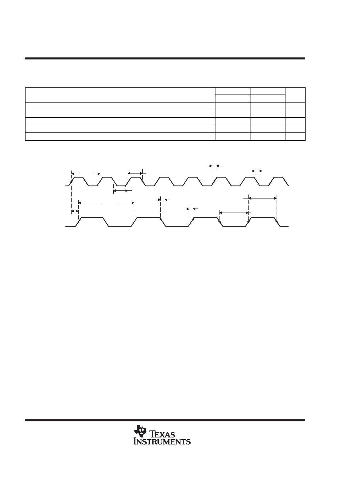
serial port receive timing
timing requirements for serial port receive [H = 0.5 t
c(CO)
] (see Figure 21)
’549-66 ’549-80
MIN MAX MIN MAX
UNIT
t
c(SCK)
Cycle time, serial port clock 6H † 6H † ns
t
f(SCK)
Fall time, serial port clock 6 6 ns
t
r(SCK)
Rise time, serial port clock 6 6 ns
t
w(SCK)
Pulse duration, serial port clock low/high 3H 3H ns
t
su(FSR)
Setup time, FSR before CLKR falling edge 6 4 ns
t
h(FSR)
Hold time, FSR after CLKR falling edge 6 4 ns
t
h(DR)
Hold time, DR after CLKR falling edge 6 6 ns
t
su(DR)
Setup time, DR before CLKR falling edge 6 6 ns
†
The serial port design is fully static and, therefore, can operate with t
c(SCK)
approaching ∞. It is characterized approaching an input frequency
of 0 Hz but tested at a much higher frequency to minimize test time.
Bit
DR
FSR
CLKR
8/167/1521
t
su(DR)
t
su(FSR)
t
h(FSR)
t
w(SCK)
t
r(SCK)
t
f(SCK)
t
w(SCK)
t
h(DR)
t
c(SCK)
Figure 21. Serial Port Receive Timing

TMS320LC549
FIXED-POINT DIGITAL SIGNAL PROCESSOR
SPRS077B – SEPTEMBER 1998 – REVISED FEBRUARY 2000
42
POST OFFICE BOX 1443 • HOUSTON, TEXAS 77251–1443
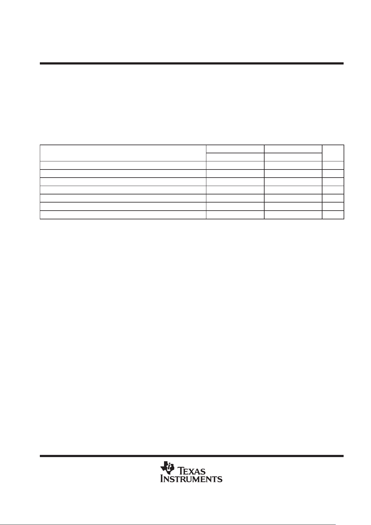
serial port transmit timing
switching characteristics over recommended operating conditions for serial port transmit with
external clocks and frames (see Figure 22)
’549-66 ’549-80
PARAMETER
MIN MAX MIN MAX
UNIT
t
d(DX)
Delay time, DX valid after CLKX rising 25 25 ns
t
h(DX)
Hold time, DX valid after CLKX rising –5 – 5 ns
t
dis(DX)
Disable time, DX after CLKX rising 40 40 ns
timing requirements for serial port transmit with external clocks and frames [H = 0.5t
c(CO)
]
(see Figure 22)
’549-66 ’549-80
MIN MAX MIN MAX
UNIT
t
c(SCK)
Cycle time, serial port clock 6H
†
6H
†
ns
t
d(FSX)
Delay time, FSX after CLKX rising edge 2H–5 2H–3 ns
t
h(FSX)
Hold time, FSX after CLKX falling edge (see Note 1) 6 6 ns
t
h(FSX)H
Hold time, FSX after CLKX rising edge (see Note 1) 2H–5
‡
2H–3
‡
ns
t
f(SCK)
Fall time, serial port clock 6 6 ns
t
r(SCK)
Rise time, serial port clock 6 6 ns
t
w(SCK)
Pulse duration, serial port clock low/high 3H 3H ns
†
The serial port design is fully static and, therefore, can operate with t
c(SCK)
approaching ∞. It is characterized approaching an input frequency
of 0 Hz but tested at a much higher frequency to minimize test time.
‡
If the FSX pulse does not meet this specification, the first bit of serial data is driven on DX until the falling edge of FSX. After the falling edge of
FSX, data is shifted out on DX pin. The transmit buffer-empty interrupt is generated when the t
h(FSX) and th(FSX)H
specification is met.
NOTE 1: Internal clock with external FSX and vice versa are also allowable. However, FSX timings to CLKX always are defined depending on
the source of FSX, and CLKX timings always are dependent upon the source of CLKX. Specifically, the relationship of FSX to CLKX
is independent of the source of CLKX.
DX Bit
FSX
CLKX
8/167/1521
t
h(DX)
t
d(DX)
t
w(SCK)
t
w(SCK)
t
c(SCK)
t
d(FSX)
t
h(FSX)H
t
h(FSX)
t
dis(DX)
t
r(SCK)
t
f(SCK)
Figure 22. Serial Port Transmit Timing With External Clocks and Frames

TMS320LC549
FIXED-POINT DIGITAL SIGNAL PROCESSOR
SPRS077B – SEPTEMBER 1998 – REVISED FEBRUARY 2000
43
POST OFFICE BOX 1443 • HOUSTON, TEXAS 77251–1443
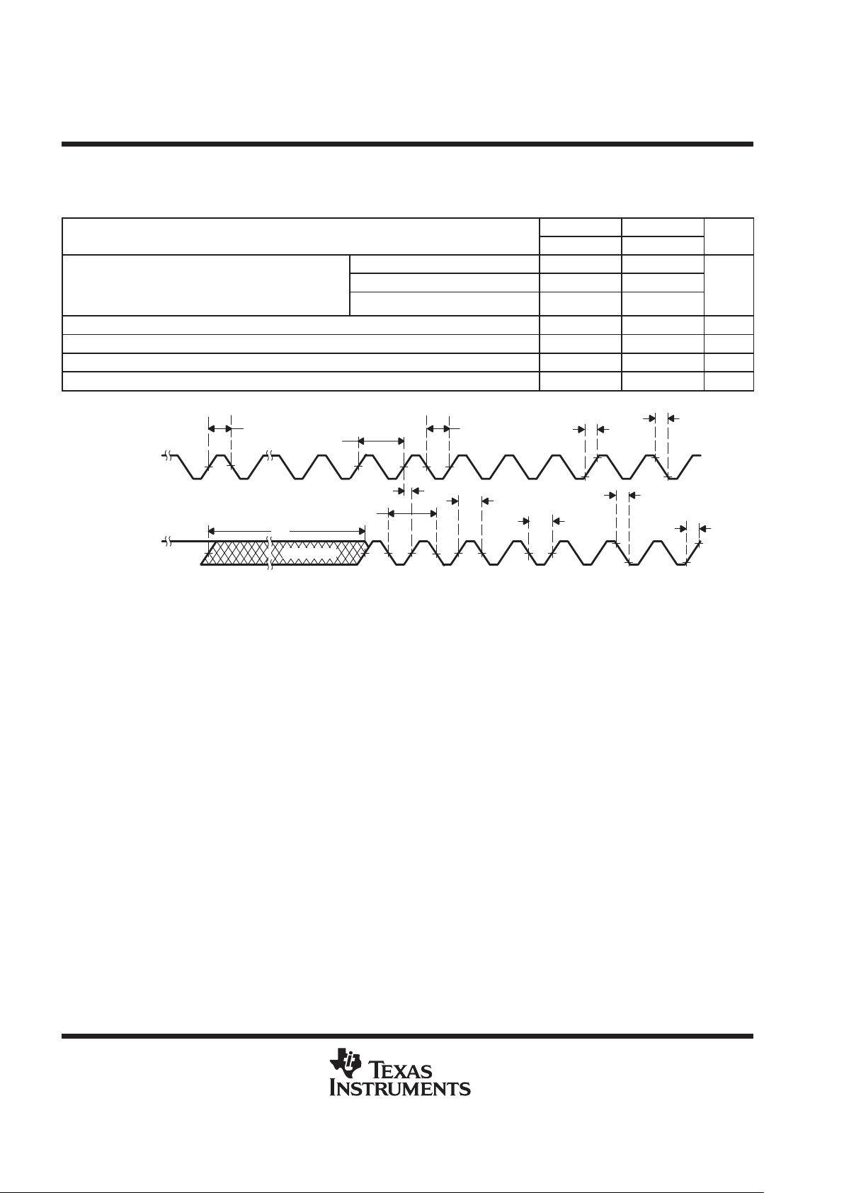
serial port transmit timing (continued)
switching characteristics over recommended operating conditions for serial port transmit with
internal clocks and frames [H = 0.5t
c(CO)
] (see Figure 23)
’549-66 ’549-80
PARAMETER
MIN TYP MAX MIN TYP MAX
UNIT
t
c(SCK)
Cycle time, serial port clock 8H 8H ns
t
d(FSX)
Delay time, CLKX rising to FSX 15 7 ns
t
d(DX)
Delay time, CLKX rising to DX 15 7 ns
t
dis(DX)
Disable time, CLKX rising to DX 20 20 ns
t
h(DX)
Hold time, DX valid after CLKX rising edge – 5 – 2 ns
t
f(SCK)
Fall time, serial port clock 4 3 ns
t
r(SCK)
Rise time, serial port clock 4 3 ns
t
w(SCK)
Pulse duration, serial port clock low/high 4H–8 4H–4 ns
DX
FSX
CLKX
8/167/1521
t
h(DX)
t
w(SCK)
t
c(SCK)
t
d(FSX)
t
d(FSX)
t
d(DX)
t
dis(DX)
t
w(SCK)
t
r(SCK)
t
f(SCK)
Figure 23. Serial Port Transmit Timing With Internal Clocks and Frames

TMS320LC549
FIXED-POINT DIGITAL SIGNAL PROCESSOR
SPRS077B – SEPTEMBER 1998 – REVISED FEBRUARY 2000
44
POST OFFICE BOX 1443 • HOUSTON, TEXAS 77251–1443
buffered serial port receive timing
timing requirements (see Figure 24)
’549-66 ’549-80
MIN MAX MIN MAX
UNIT
t
c(SCK)
Cycle time, serial port clock 20
†
20
†
ns
t
f(SCK)
Fall time, serial port clock 4 4 ns
t
r(SCK)
Rise time, serial port clock 4 4 ns
t
w(SCK)
Pulse duration, serial port clock low/high 6 6 ns
t
su(BFSR)
Setup time, BFSR before BCLKR falling edge (see Note 2) 2 2 ns
t
h(BFSR)
Hold time, BFSR after BCLKR falling edge (see Note 2) 7 t
c(SCK)
–2
‡
7 t
c(SCK)
–2
‡
ns
t
su(BDR)
Setup time, BDR before BCLKR falling edge 0 0 ns
t
h(BDR)
Hold time, BDR after BCLKR falling edge 7 7 ns
†
The serial port design is fully static and therefore can operate with t
c(SCK)
approaching infinity . It is characterized approaching an input frequency
of 0 Hz but tested at a much higher frequency to minimize test time.
‡
First bit is read when BFSR is sampled low by BCLKR clock.
NOTE 2: Timings for BCLKR and BFSR are given with polarity bits (BCLKP and BFSP) set to 0.
t
w(SCK)
t
w(SCK)
BCLKR
BFSR
BDR
1 2 8/10/12/16
t
su(BDR)
t
c(SCK)
t
su(BFSR)
t
h(BFSR)
t
h(BDR)
t
r(SCK)
t
f(SCK)
Figure 24. Buffered Serial Port Receive Timing

TMS320LC549
FIXED-POINT DIGITAL SIGNAL PROCESSOR
SPRS077B – SEPTEMBER 1998 – REVISED FEBRUARY 2000
45
POST OFFICE BOX 1443 • HOUSTON, TEXAS 77251–1443
buffered serial port transmit timing of external frames
switching characteristics over recommended operating conditions (see Figure 25)
’549-66 ’549-80
PARAMETER
MIN MAX MIN MAX
UNIT
t
d(BDX)
Delay time, BDX valid after BCLKX rising 18 18 ns
t
dis(BDX)
Disable time, BDX after BCLKX rising 4 6 4 6 ns
t
dis(BDX)pcm
Disable time, PCM mode, BDX after BCLKX rising 6 6 ns
t
en(BDX)pcm
Enable time, PCM mode, BDX after BCLKX rising 8 8 ns
t
h(BDX)
Hold time, BDX valid after BCLKX rising 2 2 ns
timing requirements (see Figure 25)
’549-66 ’549-80
MIN MAX MIN MAX
UNIT
t
c(SCK)
Cycle time, serial port clock 20
†
20
†
ns
t
f(SCK)
Fall time, serial port clock 4 4 ns
t
r(SCK)
Rise time, serial port clock 4 4 ns
t
w(SCK)
Pulse duration, serial port clock low/high 6 6 ns
t
h(BFSX)
Hold time, BFSX after CLKX falling edge (see Notes 3 and 4) 6 t
c(SCK)
–6
‡
6 t
c(SCK)
–6‡ns
t
su(BFSX)
Setup time, FSX before CLKX falling edge (see Notes 3 and 4) 6 6 ns
†
The serial port design is fully static and therefore can operate with t
c(SCK)
approaching infinity . It is characterized approaching an input frequency
of 0 Hz but tested at a much higher frequency to minimize test time.
‡
If BFSX does not meet this specification, the first bit of the serial data is driven on BDX until BFSX goes low (sampled on falling edge of BCLKX).
After falling edge of the BFSX, data will be shifted out on the BDX pin.
NOTES: 3. Internal clock with external BFSX and vice versa are also allowable. However, BFSX timings to BCLKX always are defined
depending on the source of BFSX, and BCLKX timings always are dependent upon the source of BCLKX.
4. Timings for BCLKX and BFSX are given with polarity bits (BCLKP and BFSP) set to 0.

TMS320LC549
FIXED-POINT DIGITAL SIGNAL PROCESSOR
SPRS077B – SEPTEMBER 1998 – REVISED FEBRUARY 2000
46
POST OFFICE BOX 1443 • HOUSTON, TEXAS 77251–1443
buffered serial port transmit timing of external frames (continued)
8/10/12/1621
BDX
BFSX
BCLKX
t
dis(BDX)
t
w(SCK)
t
h(BDX)
t
d(BDX)
t
w(SCK)
t
c(SCK)
t
su(BFSX)
t
h(BFSX)
t
r(SCK)
t
f(SCK)
Figure 25. Buffered Serial Port Transmit Timing of External Clocks and External Frames

TMS320LC549
FIXED-POINT DIGITAL SIGNAL PROCESSOR
SPRS077B – SEPTEMBER 1998 – REVISED FEBRUARY 2000
47
POST OFFICE BOX 1443 • HOUSTON, TEXAS 77251–1443
buffered serial port transmit timing of internal frame and internal clock
switching characteristics over recommended operating conditions [H = 0.5t
c(CO)
] (see Figure 26)
’549-66 ’549-80
PARAMETER
MIN MAX MIN MAX
UNIT
t
c(SCK)
Cycle time, serial port clock, internal clock 20 62H 20 62H ns
t
d(BFSX)
Delay time, BFSX after BCLKX rising edge (see Notes 3 and 4) 0 7 0 7 ns
t
d(BDX)
Delay time, BDX valid after BCLKX rising edge 7 7 ns
t
dis(BDX)
Disable time, BDX after BCLKX rising edge 0 5 0 5 ns
t
dis(BDX)pcm
Disable time, PCM mode, BDX after BCLKX rising edge 5 5 ns
t
en(BDX)pcm
Enable time, PCM mode, BDX after BCLKX rising edge 7 7 ns
t
h(BDX)
Hold time, BDX valid after BCLKX rising edge – 1 – 1 ns
t
f(SCK)
Fall time, serial port clock 3.5 3.5 ns
t
r(SCK)
Rise time, serial port clock 3.5 3.5 ns
t
w(SCK)
Pulse duration, serial port clock low/high 6 6 ns
NOTES: 3. Internal clock with external BFSX and vice versa are also allowable. However, BFSX timings to BCLKX always are defined
depending on the source of BFSX, and BCLKX timings always are dependent upon the source of BCLKX.
4. Timings for BCLKX and BFSX are given with polarity bits (BCLKP and BFSP) set to 0.
8/10/12/1621
BDX
BFSX
BCLKX
t
c(SCK)
t
d(BFSX)
t
d(BFSX)
t
dis(BDX)
t
w(SCK)
t
h(BDX)
t
d(BDX)
t
w(SCK)
t
r(SCK)
t
f(SCK)
Figure 26. Buffered Serial Port Transmit Timing of Internal Clocks and Internal Frames

TMS320LC549
FIXED-POINT DIGITAL SIGNAL PROCESSOR
SPRS077B – SEPTEMBER 1998 – REVISED FEBRUARY 2000
48
POST OFFICE BOX 1443 • HOUSTON, TEXAS 77251–1443
serial-port receive timing in TDM mode
timing requirements [H = 0.5t
c(CO)
] (see Figure 27)
’549-66 ’549-80
MIN MAX MIN MAX
UNIT
t
c(SCK)
Cycle time, serial-port clock 16H
†
16H
†
ns
t
f(SCK)
Fall time, serial-port clock 6 6 ns
t
r(SCK)
Rise time, serial-port clock 6 6 ns
t
w(SCK)
Pulse duration, serial-port clock low/high 8H 8H ns
t
su(TD-TCH)
Setup time, TDAT/TADD before TCLK rising edge 10 10 ns
t
h(TCH-TD)
Hold time, TDAT/TADD after TCLK rising edge 1 1 ns
t
su(TF-TCH)
Setup time, TFRM before TCLK rising edge‡ 10 10 ns
t
h(TCH-TF)
Hold time, TFRM after TCLK rising edge‡ 10 10 ns
†
The serial-port design is fully static and, therefore, can operate with t
c(SCK)
approaching infinity . It is characterized approaching an input frequency
of 0 Hz but tested at a much higher frequency to minimize test time.
‡
TFRM timing and waveforms shown in Figure 27 are for external TFRM. TFRM can also be configured as internal. The TFRM internal case is
illustrated in the transmit timing diagram in Figure 28.

TMS320LC549
FIXED-POINT DIGITAL SIGNAL PROCESSOR
SPRS077B – SEPTEMBER 1998 – REVISED FEBRUARY 2000
49
POST OFFICE BOX 1443 • HOUSTON, TEXAS 77251–1443
serial-port receive timing in TDM mode (continued)
B2B11
A3
B12
A2A0 A1
B0B1
B13B14
B15
B0
t
su(TD-TCH)
t
h(TCH-TD)
t
c(SCK)
TFRM
TADD
TDAT
TCLK
t
h(TCH-TF)
t
su(TF-TCH)
A7A4
t
w(SCK)
t
w(SCK)
t
r(SCK)
t
f(SCK)
Figure 27. Serial-Port Receive Timing in TDM Mode

TMS320LC549
FIXED-POINT DIGITAL SIGNAL PROCESSOR
SPRS077B – SEPTEMBER 1998 – REVISED FEBRUARY 2000
50
POST OFFICE BOX 1443 • HOUSTON, TEXAS 77251–1443
serial-port transmit timing in TDM mode
switching characteristics over recommended operating conditions [H = 0.5t
c(CO)
] (see Figure 28)
’549-66 ’549-80
PARAMETER
MIN MAX MIN MAX
UNIT
t
h(TCH-TDV)
Hold time, TDAT/TADD valid after TCLK rising edge, TCLK external 1 1 ns
t
h(TCH-TDV)
Hold time, TDAT/TADD valid after TCLK rising edge, TCLK internal 1 1 ns
Delay time, TFRM valid after TCLK rising edge TCLK ext
†
H – 3 3H + 22 H – 3 3H+22
t
d(TCH-TFV)
Delay time, TFRM valid after TCLK rising edge, TCLK int
†
H – 3 3H + 12 H – 3 3H+12
ns
Delay time, TCLK to valid TDAT/TADD, TCLK ext 25 25
t
d(TC-TDV)
Delay time, TCLK to valid TDAT/TADD, TCLK int 18 18
ns
†
TFRM timing and waveforms shown in Figure 28 are for internal TFRM. TFRM can also be configured as external. The TFRM external case is
illustrated in the receive timing diagram in Figure 27.

TMS320LC549
FIXED-POINT DIGITAL SIGNAL PROCESSOR
SPRS077B – SEPTEMBER 1998 – REVISED FEBRUARY 2000
51
POST OFFICE BOX 1443 • HOUSTON, TEXAS 77251–1443
serial-port transmit timing in TDM mode (continued)
timing requirements [H = 0.5t
c(CO)
] (see Figure 28)
’549-66 ’549-80
MIN MAX MIN MAX
UNIT
t
c(SCK)
Cycle time, serial-port clock 16H
†
‡
16H
†
‡
ns
t
f(SCK)
Fall time, serial-port clock 6 6 ns
t
r(SCK)
Rise time, serial-port clock 6 6 ns
t
w(SCK)
Pulse duration, serial-port clock low/high 8H
†
8H
†
ns
†
When SCK is generated internally, this value is typical.
‡
The serial-port design is fully static and, therefore, can operate with t
c(SCK)
approaching 1. It is characterized approaching an input frequency
of 0 Hz but tested as a much higher frequency to minimize test time.
A7
B2B8 B7
A3
B12
A2
A0
A1
B0B1
B13B14B0
t
w(SCK)
t
w(SCK)
t
h(TCH-TDV)
t
d(TCH-TFV)
TFRM
TADD
TDAT
TCLK
B15
t
c(SCK)
t
d(TC-TDV)
t
h(TCH-TDV)
t
d(TCH-TFV)
t
d(TC-TDV)
t
r(SCK)
t
f(SCK)
Figure 28. Serial-Port Transmit Timing in TDM Mode

TMS320LC549
FIXED-POINT DIGITAL SIGNAL PROCESSOR
SPRS077B – SEPTEMBER 1998 – REVISED FEBRUARY 2000
52
POST OFFICE BOX 1443 • HOUSTON, TEXAS 77251–1443
host-port interface timing
switching characteristics over recommended operating conditions [H = 0.5t
c(CO)
]
(see N otes 5 and 6) (see Figure 29 through Figure 32)
’549-66
PARAMETER
MIN MAX
UNIT
t
d(DSL-HDV)
Delay time, DS low to HD driven 5 12 ns
Case 1: Shared-access mode if
t
w(DSH)
< 7H
7H+20–t
w(DSH)
Delay time, HDS falling to HD valid for first byte
Case 2: Shared-access mode if
t
w(DSH)
> 7H
20
t
d(HEL-HDV1)
Delay time, HDS falling to HD valid for first byte
of a non-subsequent read: → max 20 ns
†‡
Case 3: Host-only mode if
t
w(DSH)
< 20 ns
40–t
w(DSH)
ns
Case 4: Host-only mode if
t
w(DSH)
> 20 ns
20
t
d(DSL-HDV2)
Delay time, DS low to HD valid, second byte 5
‡
20 ns
t
d(DSH-HYH)
Delay time, DS high to HRDY high 10H+10 ns
t
su(HDV-HYH)
Setup time, HD valid before HRDY rising edge 3H–10 ns
t
h(DSH-HDV)R
Hold time, HD valid after DS rising edge, read 0 12 ns
t
d(COH-HYH)
Delay time, CLKOUT rising edge to HRDY high 10 ns
t
d(DSH-HYL)
Delay time, HDS or HCS high to HRDY low 12 ns
t
d(COH-HTX)
Delay time, CLKOUT rising edge to HINT change 15 ns
†
Host-only mode timings apply for read accesses to HPIC or HPIA, write accesses to BOB, and resetting DSPINT or HINT to 0 in shared-access
mode. HRDY does not go low for these accesses.
‡
Shared-access mode timings will be met automatically if HRDY is used.
NOTES: 5. SAM = shared-access mode, HOM = host-only mode
HAD stands for HCNTRL0, HCNTRL1, and HR/W
.
HDS
refers to either HDS1 or HDS2.
DS
refers to the logical OR of HCS and HDS.
6. On host read accesses to the HPI, the setup time of HD before DS
rising edge depends on the host waveforms and cannot be
specified here.

TMS320LC549
FIXED-POINT DIGITAL SIGNAL PROCESSOR
SPRS077B – SEPTEMBER 1998 – REVISED FEBRUARY 2000
53
POST OFFICE BOX 1443 • HOUSTON, TEXAS 77251–1443
host-port interface timing (continued)
switching characteristics over recommended operating conditions [H = 0.5t
c(CO)
]
(see Notes 5 and 6) (see Figure 29 through Figure 32) (continued)
’549-80
PARAMETER
MIN MAX
UNIT
t
d(DSL-HDV)
Delay time, DS low to HD driven 5 12 ns
Case 1: Shared-access mode if
t
w(DSH)
< 7H
7H+20–t
w(DSH)
Delay time, HDS falling to HD valid for first byte
Case 2: Shared-access mode if
t
w(DSH)
> 7H
20
t
d(HEL-HDV1)
Delay time, HDS falling to HD valid for first byte
of a non-subsequent read: → max 20 ns
†‡
Case 3: Host-only mode if
t
w(DSH)
< 20 ns
40–t
w(DSH)
ns
Case 4: Host-only mode if
t
w(DSH)
> 20 ns
20
t
d(DSL-HDV2)
Delay time, DS low to HD valid, second byte 5
‡
20 ns
t
d(DSH-HYH)
Delay time, DS high to HRDY high 10H+10 ns
t
su(HDV-HYH)
Setup time, HD valid before HRDY rising edge 3H–10 ns
t
h(DSH-HDV)R
Hold time, HD valid after DS rising edge, read 0 12 ns
t
d(COH-HYH)
Delay time, CLKOUT rising edge to HRDY high 10 ns
t
d(DSH-HYL)
Delay time, HDS or HCS high to HRDY low 12 ns
t
d(COH-HTX)
Delay time, CLKOUT rising edge to HINT change 15 ns
†
Host-only mode timings apply for read accesses to HPIC or HPIA, write accesses to BOB, and resetting DSPINT or HINT to 0 in shared-access
mode. HRDY does not go low for these accesses.
‡
Shared-access mode timings will be met automatically if HRDY is used.
NOTES: 5. SAM = shared-access mode, HOM = host-only mode
HAD stands for HCNTRL0, HCNTRL1, and HR/W
.
HDS
refers to either HDS1 or HDS2.
DS
refers to the logical OR of HCS and HDS.
6. On host read accesses to the HPI, the setup time of HD before DS
rising edge depends on the host waveforms and cannot be
specified here.

TMS320LC549
FIXED-POINT DIGITAL SIGNAL PROCESSOR
SPRS077B – SEPTEMBER 1998 – REVISED FEBRUARY 2000
54
POST OFFICE BOX 1443 • HOUSTON, TEXAS 77251–1443
host-port interface timing (continued)
timing requirements [H = 0.5t
c(CO)
] (see Note 5, Figure 29 through Figure 32)
’549-66 ’549-80
MIN MAX MIN MAX
UNIT
t
su(HBV-DSL)
Setup time, HAD/HBIL valid before DS or HAS falling edge 10 10 ns
t
h(DSL-HBV)
Hold time, HAD/HBIL valid after DS or HAS falling edge 5 5 ns
t
su(HSL-DSL)
Setup time, HAS low before DS falling edge 12 12 ns
t
w(DSL)
Pulse duration, DS low 30
†
30
†
ns
t
w(DSH)
Pulse duration, DS high 10 10 ns
Cycle time, DS rising
Case 1: HOM access timings
(see Access Timing Without HRDY)
50 50
t
c(DSH-DSH)
†
Cycle time, DS rising
edge to next DS rising
edge
Case 2a: SAM accesses and HOM active writes
to DSPINT or HINT.
(see Access Timings With HRDY)
10H 10H
ns
t
su(HDV-DSH)
Setup time, HD valid before DS rising edge 12 12 ns
t
d(DSH-HSL)
‡
Delay time, DS high to next HAS low 10H 10H ns
t
h(DSH – HDV)W
Hold time, HD valid after DS rising edge, write 3 3 ns
†
A host not using HRDY should meet the 10H requirement all the time unless a software handshake is used to change the access rate according
to the HPI mode.
‡
Must only be met if HAS
is going low when not accessing the HPI (as would be the case where multiple devices are being driven by one host).
NOTE 5: SAM = shared-access mode, HOM = host-only mode
HAD stands for HCNTRL0, HCNTRL1, and HR/W
.
HDS
refers to either HDS1 or HDS2.
DS
refers to the logical OR of HCS and HDS.

TMS320LC549
FIXED-POINT DIGITAL SIGNAL PROCESSOR
SPRS077B – SEPTEMBER 1998 – REVISED FEBRUARY 2000
55
POST OFFICE BOX 1443 • HOUSTON, TEXAS 77251–1443
host-port interface timing (continued)
HBIL
HAD
t
h(DSL-HBV)
t
su(HBV-DSL)
t
h(DSL-HBV)
FIRST BYTE SECOND BYTE
HCS
HDS
t
w(DSL)
t
c(DSH-DSH)
HD
Read
t
h(DSH-HDV)R
HD
Write
t
h(DSH-HDV)W
t
su(HDV-DSH)
t
su(HBV-DSL)
t
d(DSL-HDV2)
t
w(DSH)
t
w(DSH)
t
w(DSL)
t
h(DSH-HDV)
t
su(HDV-DSH)
Valid
Valid Valid
Valid Valid
Valid
Valid
t
d(HEL-HDV1)
t
d(DSL-HDV)
t
h(DSH-HDV)
Figure 29. Read/Write Access Timings Without HRDY or HAS

TMS320LC549
FIXED-POINT DIGITAL SIGNAL PROCESSOR
SPRS077B – SEPTEMBER 1998 – REVISED FEBRUARY 2000
56
POST OFFICE BOX 1443 • HOUSTON, TEXAS 77251–1443
host-port interface timing (continued)
FIRST BYTE SECOND BYTE
HAD
t
su(HSL-DSL)
t
su(HBV-DSL)
HBIL
HCS
HDS
HAS
t
w(DSL)
t
c(DSH-DSH)
HD
Read
t
h(DSH-HDV)R
HD
Write
t
h(DSH-HDV)W
Valid Valid
Valid
Valid
t
d(DSL-HDV2)
t
su(HDV-DSH)
t
su(HDV-DSH)
t
w(DSH)
t
d(DSL-HDV)
t
d(HEL-HDV1)
t
h(DSH-HDV)W
t
su(HBV-DSL)
†
Valid Valid Valid
t
h(DSH-HDV)R
t
h(DSL-HBV)
†
t
h(DSL-HBV)
t
d(DSH-HSL)
†
When HAS
is tied to V
DD
Figure 30. Read/Write Access Timings Using HAS Without HRDY

TMS320LC549
FIXED-POINT DIGITAL SIGNAL PROCESSOR
SPRS077B – SEPTEMBER 1998 – REVISED FEBRUARY 2000
57
POST OFFICE BOX 1443 • HOUSTON, TEXAS 77251–1443
host-port interface timing (continued)
FIRST BYTE SECOND BYTE
t
h(DSL-HBV)
†
HRDY
t
d(DSH-HYL)
CLKOUT
t
d(COH-HYH)
HINT
t
d(COH-HTX)
t
su(HBV-DSL)
†
t
su(HSL-DSL)
t
h(DSL-HBV)
HCS
HDS
HAS
t
w(DSL)
t
c(DSH-DSH)
HD
READ
t
h(DSH-HDV)R
HD
WRITE
t
h(DSH-HDV)W
t
h(DSH-HDV)W
Valid Valid
Valid
Valid
t
su(HDV-DSH)
t
su(HDV-DSH)
t
w(DSH)
t
d(DSL-HDV2)
HAD
HBIL
t
su(HDV-HYH)
t
d(DSH-HYH)
t
su(HBV-DSL)
t
d(DSL-HDV)
t
d(HEL-HDV1)
t
h(DSH-HDV)R
t
d(DSH-HSL)
†
When HAS is tied to V
DD
Figure 31. Read/Write Access Timing With HRDY

TMS320LC549
FIXED-POINT DIGITAL SIGNAL PROCESSOR
SPRS077B – SEPTEMBER 1998 – REVISED FEBRUARY 2000
58
POST OFFICE BOX 1443 • HOUSTON, TEXAS 77251–1443
host-port interface timing (continued)
HRDY
HCS
t
d(DSH-HYH)
HDS
t
d(DSH-HYL)
Figure 32. HRDY Signal When HCS is Always Low

TMS320LC549
FIXED-POINT DIGITAL SIGNAL PROCESSOR
SPRS077B – SEPTEMBER 1998 – REVISED FEBRUARY 2000
59
POST OFFICE BOX 1443 • HOUSTON, TEXAS 77251–1443
MECHANICAL DATA
PGE (S-PQFP-G144) PLASTIC QUAD FLATPACK
4040147/C 10/96
0,27
72
0,17
37
73
0,13 NOM
0,25
0,75
0,45
0,05 MIN
36
Seating Plane
Gage Plane
108
109
144
SQ
SQ
22,20
21,80
1
19,80
17,50 TYP
20,20
1,35
1,45
1,60 MAX
M
0,08
0°–ā7°
0,08
0,50
NOTES: A. All linear dimensions are in millimeters.
B. This drawing is subject to change without notice.
C. Falls within JEDEC MS-026
Thermal Resistance Characteristics
PARAMETER
°C/W
R
ΘJA
56
R
ΘJC
5

TMS320LC549
FIXED-POINT DIGITAL SIGNAL PROCESSOR
SPRS077B – SEPTEMBER 1998 – REVISED FEBRUARY 2000
60
POST OFFICE BOX 1443 • HOUSTON, TEXAS 77251–1443
MECHANICAL DATA
GGU (S-PBGA-N144) PLASTIC BALL GRID ARRAY PACKAGE
0,80
0,10
M
0,08
0,80
9,60 TYP
12 1310 118967
N
M
K
L
J
H
42 3
F
E
C
B
D
A
1
G
5
Seating Plane
4073221/A 11/96
SQ
11,90
12,10
0,95
0,35
0,45
0,45
0,55
0,85
0,08
0,12
1,40 MAX
NOTES: A. All linear dimensions are in millimeters.
B. This drawing is subject to change without notice.
C. MicroStar BGA configuration
Thermal Resistance Characteristics
PARAMETER
°C/W
R
ΘJA
38
R
ΘJC
5

IMPORTANT NOTICE
T exas Instruments and its subsidiaries (TI) reserve the right to make changes to their products or to discontinue
any product or service without notice, and advise customers to obtain the latest version of relevant information
to verify, before placing orders, that information being relied on is current and complete. All products are sold
subject to the terms and conditions of sale supplied at the time of order acknowledgement, including those
pertaining to warranty, patent infringement, and limitation of liability.
TI warrants performance of its semiconductor products to the specifications applicable at the time of sale in
accordance with TI’s standard warranty. Testing and other quality control techniques are utilized to the extent
TI deems necessary to support this warranty. Specific testing of all parameters of each device is not necessarily
performed, except those mandated by government requirements.
CERT AIN APPLICATIONS USING SEMICONDUCTOR PRODUCTS MAY INVOLVE POTENTIAL RISKS OF
DEATH, PERSONAL INJURY, OR SEVERE PROPERTY OR ENVIRONMENTAL DAMAGE (“CRITICAL
APPLICATIONS”). TI SEMICONDUCTOR PRODUCTS ARE NOT DESIGNED, AUTHORIZED, OR
WARRANTED TO BE SUITABLE FOR USE IN LIFE-SUPPORT DEVICES OR SYSTEMS OR OTHER
CRITICAL APPLICATIONS. INCLUSION OF TI PRODUCTS IN SUCH APPLICA TIONS IS UNDERSTOOD T O
BE FULLY AT THE CUSTOMER’S RISK.
In order to minimize risks associated with the customer’s applications, adequate design and operating
safeguards must be provided by the customer to minimize inherent or procedural hazards.
TI assumes no liability for applications assistance or customer product design. TI does not warrant or represent
that any license, either express or implied, is granted under any patent right, copyright, mask work right, or other
intellectual property right of TI covering or relating to any combination, machine, or process in which such
semiconductor products or services might be or are used. TI’s publication of information regarding any third
party’s products or services does not constitute TI’s approval, warranty or endorsement thereof.
Copyright 2000, Texas Instruments Incorporated
 Loading...