

Page 1

ADVANCEINFORMATION
TMS320C6748
www.ti.com
SPRS590B–JUNE 2009–REVISED AUGUST 2010
TMS320C6748 Fixed/Floating-Point DSP
Check for Samples: TMS320C6748
1 TMS320C6748 Fixed/Floating-Point DSP
1.1 Features
12
• Highlights
– 375/456-MHz C674x Fixed/Floating-Point
VLIW DSP – Six ALU (32-/40-Bit) Functional Units
– Enhanced Direct-Memory-Access Controller • Supports 32-Bit Integer, SP (IEEE Single
(EDMA3) Precision/32-Bit) and DP (IEEE Double
– Serial ATA (SATA) Controller
– DDR2/Mobile DDR Memory Controller
– Two Multimedia Card (MMC)/Secure Digital
(SD) Card Interface
– LCD Controller
– Video Port Interface (VPIF)
– 10/100 Mb/s Ethernet MAC (EMAC):
– Programmable Real-Time Unit Subsystem
– Three Configurable UART Modules
– USB 1.1 OHCI (Host) With Integrated PHY
– USB 2.0 OTG Port With Integrated PHY
– One Multichannel Audio Serial Port
– Two Multichannel Buffered Serial Ports
• 375/456-MHz C674x VLIW DSP
• C674x Instruction Set Features
– Superset of the C67x+™ and C64x+™ ISAs
– Up to 3648/2746 C674x MIPS/MFLOPS
– Byte-Addressable (8-/16-/32-/64-Bit Data)
– 8-Bit Overflow Protection
– Bit-Field Extract, Set, Clear
– Normalization, Saturation, Bit-Counting
– Compact 16-Bit Instructions
• C674x Two Level Cache Memory Architecture
– 32K-Byte L1P Program RAM/Cache
– 32K-Byte L1D Data RAM/Cache
– 256K -Byte L2 Unified Mapped RAM/Cache
– Flexible RAM/Cache Partition (L1 and L2)
• Enhanced Direct-Memory-Access Controller 3
(EDMA3):
– 2 Channel Controllers
– 3 Transfer Controllers
– 64 Independent DMA Channels
– 16 Quick DMA Channels
– Programmable Transfer Burst Size
• TMS320C674x Floating-Point VLIW DSP Core
– Load-Store Architecture With Non-Aligned
1
Please be aware that an important notice concerning availability, standard warranty, and use in critical applications of Texas
Instruments semiconductor products and disclaimers thereto appears at the end of this data sheet.
2TMS320C6000, C6000 are trademarks of Texas Instruments.
ADVANCE INFORMATION concerns new products in the sampling
or preproduction phaseof development. Characteristic dataand other
specifications are subjectto change without notice.
Support
– 64 General-Purpose Registers (32 Bit)
Precision/64-Bit) Floating Point
• Supports up to Four SP Additions Per
Clock, Four DP Additions Every 2 Clocks
• Supports up to Two Floating Point (SP or
DP) Reciprocal Approximation (RCPxP)
and Square-Root Reciprocal
Approximation (RSQRxP) Operations Per
Cycle
– Two Multiply Functional Units
• Mixed-Precision IEEE Floating Point
Multiply Supported up to:
– 2 SP x SP -> SP Per Clock
– 2 SP x SP -> DP Every Two Clocks
– 2 SP x DP -> DP Every Three Clocks
– 2 DP x DP -> DP Every Four Clocks
• Fixed Point Multiply Supports Two 32 x
32-Bit Multiplies, Four 16 x 16-Bit
Multiplies, or Eight 8 x 8-Bit Multiplies per
Clock Cycle, and Complex Multiples
– Instruction Packing Reduces Code Size
– All Instructions Conditional
– Hardware Support for Modulo Loop
Operation
– Protected Mode Operation
– Exceptions Support for Error Detection and
Program Redirection
• Software Support
– TI DSP/BIOS™
– Chip Support Library and DSP Library
• 128K-Byte RAM Memory
• 1.8V or 3.3V LVCMOS IOs (except for USB and
DDR2 interfaces)
• Two External Memory Interfaces:
– EMIFA
• NOR (8-/16-Bit-Wide Data)
• NAND (8-/16-Bit-Wide Data)
• 16-Bit SDRAM With 128 MB Address
Space
Copyright © 2009–2010, Texas Instruments Incorporated
Page 2

ADVANCEINFORMATION
TMS320C6748
SPRS590B–JUNE 2009–REVISED AUGUST 2010
www.ti.com
– DDR2/Mobile DDR Memory Controller – Telecom Interfaces (ST-Bus, H100)
• 16-Bit DDR2 SDRAM With 512 MB – 128-channel TDM
Address Space or
• 16-Bit mDDR SDRAM With 256 MB
Address Space
• Three Configurable 16550 type UART Modules:
– With Modem Control Signals
– 16-byte FIFO
– 16x or 13x Oversampling Option
• LCD Controller
• Two Serial Peripheral Interfaces (SPI) Each
With Multiple Chip-Selects
• Two Multimedia Card (MMC)/Secure Digital (SD)
Card Interface with Secure Data I/O (SDIO)
Interfaces
• Two Master/Slave Inter-Integrated Circuit (I2C
Bus™)
• One Host-Port Interface (HPI) With 16-Bit-Wide
Muxed Address/Data Bus For High Bandwidth
• Programmable Real-Time Unit Subsystem
(PRUSS)
– Two Independent Programmable Realtime
Unit (PRU) Cores
• 32-Bit Load/Store RISC architecture
• 4K Byte instruction RAM per core
• 512 Bytes data RAM per core
• PRU Subsystem (PRUSS) can be disabled
via software to save power
• Register 30 of each PRU is exported from
the subsystem in addition to the normal
R31 output of the PRU cores.
– Standard power management mechanism
• Clock gating
• Entire subsystem under a single PSC
clock gating domain
– Dedicated interrupt controller
– FIFO buffers for Transmit and Receive
• 10/100 Mb/s Ethernet MAC (EMAC):
– IEEE 802.3 Compliant
– MII Media Independent Interface
– RMII Reduced Media Independent Interface
– Management Data I/O (MDIO) Module
• Video Port Interface (VPIF):
– Two 8-bit SD (BT.656), Single 16-bit or Single
Raw (8-/10-/12-bit) Video Capture Channels
– Two 8-bit SD (BT.656), Single 16-bit Video
Display Channels
• Universal Parallel Port (uPP):
– High-Speed Parallel Interface to FPGAs and
Data Converters
– Data Width on Each of Two Channels is 8- to
16-bit Inclusive
– Single Data Rate or Dual Data Rate Transfers
– Supports Multiple Interfaces with START,
ENABLE and WAIT Controls
• Serial ATA (SATA) Controller:
– Supports SATA I (1.5 Gbps) and SATA II (3.0
Gbps)
– Supports all SATA Power Management
Features
– Hardware-Assisted Native Command
Queueing (NCQ) for up to 32 Entries
– Supports Port Multiplier and
Command-Based Switching
• Real-Time Clock With 32 KHz Oscillator and
Separate Power Rail
• Three 64-Bit General-Purpose Timers (Each
configurable as Two 32-Bit Timers)
• One 64-bit General-Purpose/Watchdog Timer
(Configurable as Two 32-bit General-Purpose
– Dedicated switched central resource Timers)
• USB 1.1 OHCI (Host) With Integrated PHY • Two Enhanced Pulse Width Modulators
(USB1) (eHRPWM):
• USB 2.0 OTG Port With Integrated PHY (USB0) – Dedicated 16-Bit Time-Base Counter With
– USB 2.0 High-/Full-Speed Client
– USB 2.0 High-/Full-/Low-Speed Host
– End Point 0 (Control)
– End Points 1,2,3,4 (Control, Bulk, Interrupt or
ISOC) Rx and Tx
• One Multichannel Audio Serial Port:
– Two Clock Zones and 16 Serial Data Pins
– Supports TDM, I2S, and Similar Formats
– DIT-Capable
– FIFO buffers for Transmit and Receive
• Two Multichannel Buffered Serial Ports:
– Supports TDM, I2S, and Similar Formats
– AC97 Audio Codec Interface
Period And Frequency Control
– 6 Single Edge, 6 Dual Edge Symmetric or 3
Dual Edge Asymmetric Outputs
– Dead-Band Generation
– PWM Chopping by High-Frequency Carrier
– Trip Zone Input
• Three 32-Bit Enhanced Capture Modules
(eCAP):
– Configurable as 3 Capture Inputs or 3
Auxiliary Pulse Width Modulator (APWM)
outputs
– Single Shot Capture of up to Four Event
Time-Stamps
• 361-Ball Pb-Free Plastic Ball Grid Array (PBGA)
2 TMS320C6748 Fixed/Floating-Point DSP Copyright © 2009–2010, Texas Instruments Incorporated
Submit Documentation Feedback
Product Folder Link(s): TMS320C6748
Page 3

ADVANCEINFORMATION
TMS320C6748
www.ti.com
SPRS590B–JUNE 2009–REVISED AUGUST 2010
[ZCE Suffix], 0.65-mm Ball Pitch Temperature
• 361-Ball Pb-Free Plastic Ball Grid Array (PBGA) • Community Resources
[ZWT Suffix], 0.80-mm Ball Pitch
• Commercial, Extended or Industrial
– TI E2E Community
– TI Embedded Processors Wiki
Copyright © 2009–2010, Texas Instruments Incorporated TMS320C6748 Fixed/Floating-Point DSP 3
Submit Documentation Feedback
Product Folder Link(s): TMS320C6748
Page 4

ADVANCEINFORMATION
TMS320C6748
SPRS590B–JUNE 2009–REVISED AUGUST 2010
1.2 Trademarks
DSP/BIOS, TMS320C6000, C6000, TMS320, TMS320C62x, and TMS320C67x are trademarks of Texas
Instruments.
All trademarks are the property of their respective owners.
www.ti.com
4 TMS320C6748 Fixed/Floating-Point DSP Copyright © 2009–2010, Texas Instruments Incorporated
Submit Documentation Feedback
Product Folder Link(s): TMS320C6748
Page 5

ADVANCEINFORMATION
TMS320C6748
www.ti.com
1.3 Description
The device is a Low-power applications processor based on a C674x DSP core. It provides significantly
lower power than other members of the TMS320C6000™ platform of DSPs.
The device enables OEMs and ODMs to quickly bring to market devices featuring robust operating
systems support, rich user interfaces, and high processing performance life through the maximum
flexibility of a fully integrated mixed processor solution.
The device DSP core uses a two-level cache-based architecture. The Level 1 program cache (L1P) is a
32KB direct mapped cache and the Level 1 data cache (L1D) is a 32KB 2-way set-associative cache. The
Level 2 program cache (L2P) consists of a 256KB memory space that is shared between program and
data space. L2 memory can be configured as mapped memory, cache, or combinations of the two.
Although the DSP L2 is accessible by other hosts in the system, an additional 128KB RAM shared
memory is available for use by other hosts without affecting DSP performance.
The peripheral set includes: a 10/100 Mb/s Ethernet MAC (EMAC) with a Management Data Input/Output
(MDIO) module; one USB2.0 OTG interface; one USB1.1 OHCI interface; two inter-integrated circuit (I2C)
Bus interfaces; one multichannel audio serial port (McASP) with 16 serializers and FIFO buffers; two
multichannel buffered serial ports (McBSP) with FIFO buffers; two SPI interfaces with multiple chip
selects; four 64-bit general-purpose timers each configurable (one configurable as watchdog); a
configurable 16-bit host port interface (HPI) ; up to 9 banks of 16 pins of general-purpose input/output
(GPIO) with programmable interrupt/event generation modes, multiplexed with other peripherals; three
UART interfaces (each with RTS and CTS); two enhanced high-resolution pulse width modulator
(eHRPWM) peripherals; 3 32-bit enhanced capture (eCAP) module peripherals which can be configured
as 3 capture inputs or 3 auxiliary pulse width modulator (APWM) outputs; and 2 external memory
interfaces: an asynchronous and SDRAM external memory interface (EMIFA) for slower memories or
peripherals, and a higher speed DDR2/Mobile DDR controller.
SPRS590B–JUNE 2009–REVISED AUGUST 2010
The Ethernet Media Access Controller (EMAC) provides an efficient interface between the device and a
network. The EMAC supports both 10Base-T and 100Base-TX, or 10 Mbits/second (Mbps) and 100 Mbps
in either half- or full-duplex mode. Additionally an Management Data Input/Output (MDIO) interface is
available for PHY configuration. The EMAC supports both MII and RMII interfaces.
The SATA controller provides a high-speed interface to mass data storage devices. The SATA controller
supports both SATA I (1.5 Gbps) and SATA II (3.0 Gbps).
The Universal Parallel Port (uPP) provides a high-speed interface to many types of data converters,
FPGAs or other parallel devices. The UPP supports programmable data widths between 8- to 16-bits on
each of two channels. Single-data rate and double-data rate transfers are supported as well as START,
ENABLE and WAIT signals to provide control for a variety of data converters.
A Video Port Interface (VPIF) is included providing a flexible video input/output port.
The rich peripheral set provides the ability to control external peripheral devices and communicate with
external processors. For details on each of the peripherals, see the related sections later in this document
and the associated peripheral reference guides.
The device has a complete set of development tools for the DSP. These include C compilers, a DSP
assembly optimizer to simplify programming and scheduling, and a Windows™ debugger interface for
visibility into source code execution.
Copyright © 2009–2010, Texas Instruments Incorporated TMS320C6748 Fixed/Floating-Point DSP 5
Submit Documentation Feedback
Product Folder Link(s): TMS320C6748
Page 6
ADVANCEINFORMATION
Switched Central Resource (SCR)
BOOT ROM
256KB L2 RAM
32KB
L1 RAM
32KB
L1 Pgm
AET
C674x™
DSP CPU
DSP Subsystem
JTAG Interface
System Control
Input
Clock(s)
Power/Sleep
Controller
Pin
Multiplexing
PLL/Clock
Generator
w/OSC
GeneralPurpose
Timer (x3)
Serial Interfaces
Audio Ports
McASP
w/FIFO
DMA
Peripherals
Display Internal Memory
LCD
Ctlr
128KB
RAM
External Memory InterfacesConnectivity
EDMA3
(x2)
Control Timers
ePWM
(x2)
eCAP
(x3)
EMIFA(8b/16B)
NAND/Flash
16b SDRAM
DDR2/MDDR
Controller
RTC/
32-kHz
OSC
I C
(x2)
2
SPI
(x2)
UART
(x3)
McBSP
(x2)
Video
VPIF
Parallel Port
uPP
EMAC
10/100
(MII/RMII)
MDIO
USB1.1
OHCI Ctlr
PHY
USB2.0
OTG Ctlr
PHY
HPI
MMC/SD
(8b)
(x2)
SATA
Customizable Interface
PRU Subsystem
TMS320C6748
SPRS590B–JUNE 2009–REVISED AUGUST 2010
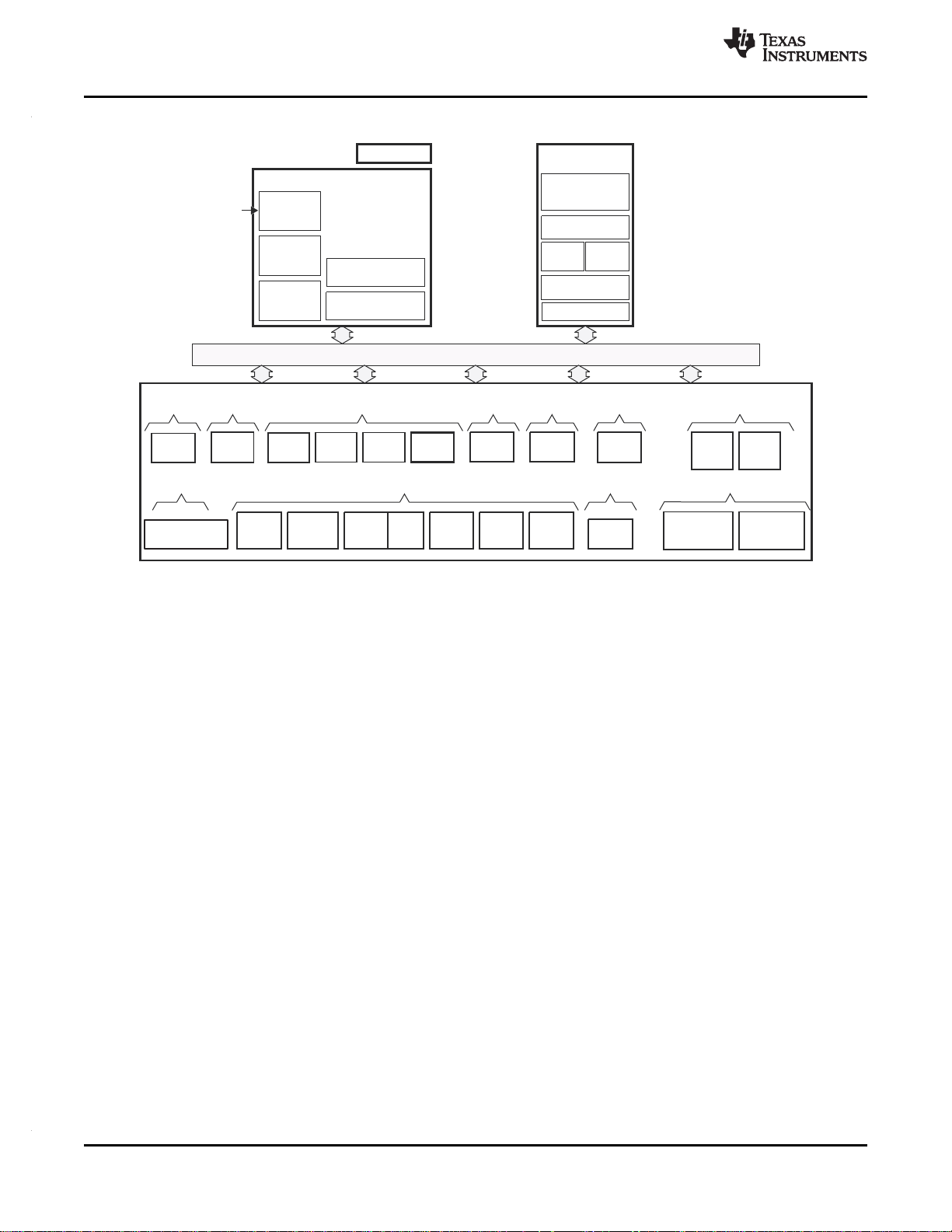
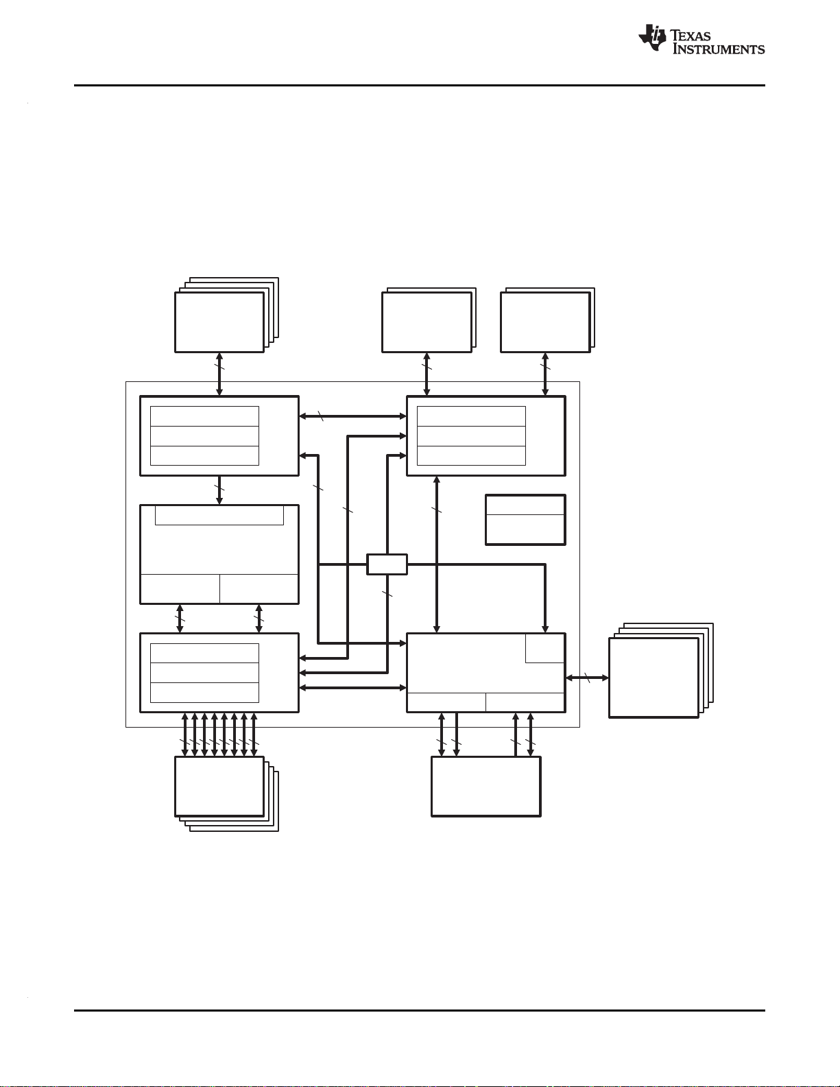
1.4 Functional Block Diagram
www.ti.com
Figure 1-1. Functional Block Diagram
6 TMS320C6748 Fixed/Floating-Point DSP Copyright © 2009–2010, Texas Instruments Incorporated
Submit Documentation Feedback
Product Folder Link(s): TMS320C6748
Page 7
ADVANCEINFORMATION
TMS320C6748
www.ti.com
SPRS590B–JUNE 2009–REVISED AUGUST 2010
1 TMS320C6748 Fixed/Floating-Point DSP ........... 1 6.6 Clock PLLs ......................................... 90
1.1 Features .............................................. 1
1.2 Trademarks .......................................... 4
1.3 Description ........................................... 5
1.4 Functional Block Diagram ............................ 6
2 Revision History ......................................... 8
3 Device Overview ........................................ 9
3.1 Documentation Support .............................. 9
3.2 Device Characteristics ............................... 9
3.3 Device Compatibility ................................ 11
3.4 DSP Subsystem .................................... 12
3.5 Memory Map Summary ............................. 23
3.6 Pin Assignments .................................... 27
3.7 Pin Multiplexing Control ............................ 30
3.8 Terminal Functions ................................. 31
3.9 Unused Pin Configurations ......................... 72
4 Device Configuration ................................. 75
4.1 Boot Modes ......................................... 75
4.2 SYSCFG Module ................................... 75
4.3 Pullup/Pulldown Resistors .......................... 78
5 Device Operating Conditions ....................... 79
5.1 Absolute Maximum Ratings Over Operating
Junction Temperature Range
(Unless Otherwise Noted) ................................. 79
5.2 Recommended Operating Conditions .............. 80
5.3 Notes on Recommended Power-On Hours (POH)
...................................................... 82
5.4 Electrical Characteristics Over Recommended
Ranges of Supply Voltage and Operating Junction
Temperature (Unless Otherwise Noted) ............ 83
6 Peripheral Information and Electrical
Specifications .......................................... 84
6.1 Parameter Information .............................. 84
6.2 Recommended Clock and Control Signal Transition
Behavior ............................................ 85
6.3 Power Supplies ..................................... 85
6.4 Reset ............................................... 86
6.5 Crystal Oscillator or External Clock Input .......... 89
6.7 Interrupts ............................................ 95
6.8 Power and Sleep Controller (PSC) ................. 99
6.9 EDMA ............................................. 104
6.10 External Memory Interface A (EMIFA) ............ 110
6.11 DDR2/mDDR Controller ........................... 121
6.12 Memory Protection Units .......................... 134
6.13 MMC / SD / SDIO (MMCSD0, MMCSD1) ......... 137
6.14 Serial ATA Controller (SATA) ..................... 140
6.15 Multichannel Audio Serial Port (McASP) .......... 145
6.16 Multichannel Buffered Serial Port (McBSP) ....... 154
6.17 Serial Peripheral Interface Ports (SPI0, SPI1) .... 164
6.18 Inter-Integrated Circuit Serial Ports (I2C) ......... 185
6.19 Universal Asynchronous Receiver/Transmitter
(UART) ............................................ 189
6.20 Universal Serial Bus OTG Controller (USB0)
[USB2.0 OTG] ..................................... 191
6.21 Universal Serial Bus Host Controller (USB1)
[USB1.1 OHCI] .................................... 198
6.22 Ethernet Media Access Controller (EMAC) ....... 199
6.23 Management Data Input/Output (MDIO) .......... 207
6.24 LCD Controller (LCDC) ............................ 209
6.25 Host-Port Interface (UHPI) ........................ 224
6.26 Universal Parallel Port (uPP) ...................... 232
6.27 Video Port Interface (VPIF) ....................... 237
6.28 Enhanced Capture (eCAP) Peripheral ............ 243
6.29 Enhanced High-Resolution Pulse-Width Modulator
(eHRPWM) ........................................ 246
6.30 Timers ............................................. 251
6.31 Real Time Clock (RTC) ........................... 253
6.32 General-Purpose Input/Output (GPIO) ............ 256
6.33 Programmable Real-Time Unit Subsystem (PRUSS)
..................................................... 260
6.34 Emulation Logic ................................... 263
7 Mechanical Packaging and Orderable
Information ............................................ 267
7.1 Device Support .................................... 267
7.2 Thermal Data for ZCE Package ................... 269
7.3 Thermal Data for ZWT Package .................. 270
Copyright © 2009–2010, Texas Instruments Incorporated Contents 7
Submit Documentation Feedback
Product Folder Link(s): TMS320C6748
Page 8
ADVANCEINFORMATION
TMS320C6748
SPRS590B–JUNE 2009–REVISED AUGUST 2010
www.ti.com
2 Revision History
NOTE: This is a placeholder for the Revision History Table for future revisions of the document.
This data manual revision history highlights the changes made to the SPRS590A device-specific data
manual to make it an SPRS590B revision.
Table 2-1. Revision History
ADDITIONS/MODIFICATIONS/DELETIONS
Global - Added MPU Content
Global - Replaced all "CLKIN" references with "OSCIN"
Global - Updated td(SCSL_SPC)S min from P to 2P
Global - Made changes in the document to reflect the following detail.
"The DSP L2 ROM is used for boot purposes and cannot be programmed with application code".
Global - Updated the pin map graphic to fix typos.
Global -
• All instances of EMU[0] updated to EMU0
• All instances of EMU[1] updated toEMU1
• All instances of UART1_RTS updated to have an overbar
• All instances of UART2_RTS updated to have an overbar
• All instances of SPI1_SCS[0] updated to have an overbar
• All instances of EMA_CS[4] updated to have an overbar
• All instances of SPI1_ENA updated to have an overbar
• All instances of SATA_TXN updated to have an overbar
• All instances of LCD_AC_ENB_CS updated to have an overbar
• All instances of DDR_CS updated to have an overbar
• All instances of UHPI_HRDY updated to have an overbar
• All instances of UHPI_HDS1 updated to have an overbar
• All instances of UHPI_HCS updated to have an overbar
Added Table 3-3 C674x L1/L2 Memory Protection Registers
Added Section 3.9 Unused Pin Configurations
Added Section 6.6.3- Dynamic Voltage and Frequency Scaling (DVFS)
AddedSection 4.3 Pullup/Pulldown Resistors
Added Section 6.14.3 - SATA Unused Signal Configuration
Added sections -Section 6.14.2 - SATA Interface, Section 6.14.2.1 - SATA Interface Schematic, Section 6.14.2.2 - Compatible SATA
Components and Modes, Section 6.14.2.3 - PCB Stackup Specifications, Section 6.14.2.4 - Routing Specifications, Section 6.14.2.5 Coupling Capacitors, Section 6.14.2.6 - SATA Interface Clock Source requirements,
Updated the Nomenclature Graphic in Section 7.1.2
8 Revision History Copyright © 2009–2010, Texas Instruments Incorporated
Submit Documentation Feedback
Product Folder Link(s): TMS320C6748
Page 9

ADVANCEINFORMATION
TMS320C6748
www.ti.com
3 Device Overview
3.1 Documentation Support
3.1.1 Related Documentation From Texas Instruments
The following documents are available on the Internet at www.ti.com. Tip: Enter the literature number in
the search box provided at www.ti.com.
DSP Reference Guides
SPRUG82 TMS320C674x DSP Cache User's Guide. Explains the fundamentals of memory caches
and describes how the two-level cache-based internal memory architecture in the
TMS320C674x digital signal processor (DSP) can be efficiently used in DSP applications.
Shows how to maintain coherence with external memory, how to use DMA to reduce
memory latencies, and how to optimize your code to improve cache efficiency. The internal
memory architecture in the C674x DSP is organized in a two-level hierarchy consisting of a
dedicated program cache (L1P) and a dedicated data cache (L1D) on the first level.
Accesses by the CPU to the these first level caches can complete without CPU pipeline
stalls. If the data requested by the CPU is not contained in cache, it is fetched from the next
lower memory level, L2 or external memory.
SPRUFE8 TMS320C674x DSP CPU and Instruction Set Reference Guide. Describes the CPU
architecture, pipeline, instruction set, and interrupts for the TMS320C674x digital signal
processors (DSPs). The C674x DSP is an enhancement of the C64x+ and C67x+ DSPs with
added functionality and an expanded instruction set.
SPRS590B–JUNE 2009–REVISED AUGUST 2010
SPRUFK5 TMS320C674x DSP Megamodule Reference Guide. Describes the TMS320C674x digital
signal processor (DSP) megamodule. Included is a discussion on the internal direct memory
access (IDMA) controller, the interrupt controller, the power-down controller, memory
protection, bandwidth management, and the memory and cache.
SPRUFK9 TMS320C674x/OMAP-L1x Processor Peripherals Overview Reference Guide. Provides
an overview and briefly describes the peripherals available on the device.
SPRUGJ7 TMS320C6748 DSP System Reference Guide .
3.2 Device Characteristics
Table 3-1 provides an overview of the device. The table shows significant features of the device, including
the capacity of on-chip RAM, peripherals, and the package type with pin count.
Copyright © 2009–2010, Texas Instruments Incorporated Device Overview 9
Submit Documentation Feedback
Product Folder Link(s): TMS320C6748
Page 10
ADVANCEINFORMATION
TMS320C6748
SPRS590B–JUNE 2009–REVISED AUGUST 2010
HARDWARE FEATURES C6748
DDR2/mDDR Controller
EMIFA
Flash Card Interface MMC and SD cards supported.
EDMA3
Timers
UART 3 (each with RTS and CTS flow control)
SPI 2 (Each with one hardware chip select)
Peripherals
Not all peripherals pins
are available at the
same time (for more
detail, see the Device
Configurations section).
On-Chip Memory
I2C 2 (both Master/Slave)
Multichannel Audio Serial Port [McASP] 1 (each with transmit/receive, FIFO buffer, 16 serializers)
Multichannel Buffered Serial Port [McBSP] 2 (each with transmit/receive, FIFO buffer, 16)
10/100 Ethernet MAC with Management Data I/O 1 (MII or RMII Interface)
eHRPWM
eCAP 3 32-bit capture inputs or 3 32-bit auxiliary PWM outputs
UHPI 1 (16-bit multiplexed address/data)
USB 2.0 (USB0) High-Speed OTG Controller with on-chip OTG PHY
USB 1.1 (USB1) Full-Speed OHCI (as host) with on-chip PHY
General-Purpose Input/Output Port 9 banks of 16-bit
LCD Controller 1
SATA Controller 1 (Support both SATA I and SATAII)
Universal Parallel Port (uPP) 1
Video Port Interface (VPIF) 1 (video in and video out)
PRU Subsystem (PRUSS) 2 Programmable PRU Cores
Size (Bytes) 448KB RAM
Organization
www.ti.com
Table 3-1. Characteristics of C6748
DDR2, 16-bit bus width, up to 150 MHz
Mobile DDR, 16-bit bus width, up to 133 MHz
Asynchronous (8/16-bit bus width) RAM, Flash,
16-bit SDRAM, NOR, NAND
64 independent channels, 16 QDMA channels,
2 channel controllers, 3 transfer controllers
4 64-Bit General Purpose (each configurable as 2 separate
32-bit timers, one configurable as Watch Dog)
4 Single Edge, 4 Dual Edge Symmetric, or
2 Dual Edge Asymmetric Outputs
DSP
32KB L1 Program (L1P)/Cache (up to 32KB)
32KB L1 Data (L1D)/Cache (up to 32KB)
256KB Unified Mapped RAM/Cache (L2)
DSP Memories can be made accessible to EDMA3 and
other peripherals.
ADDITIONAL MEMORY
128KB RAM
C674x CPU ID + CPU
Rev ID
C674x Megamodule
Revision
JTAG BSDL_ID DEVIDR0 Register 0x0B7D_102F
CPU Frequency MHz 674x DSP 375 MHz (1.2V) or 456 MHz (1.3V)
Voltage
Packages
10 Device Overview Copyright © 2009–2010, Texas Instruments Incorporated
Control Status Register (CSR.[31:16]) 0x1400
Revision ID Register (MM_REVID[15:0]) 0x0000
Core (V)
I/O (V) 1.8V or 3.3 V
13 mm x 13 mm, 361-Ball 0.65 mm pitch, PBGA (ZCE)
16 mm x 16 mm, 361-Ball 0.80 mm pitch, PBGA (ZWT)
Submit Documentation Feedback
Product Folder Link(s): TMS320C6748
1.2 V nominal for 375 MHz version
1.3 V nominal for 456 MHz version
Page 11

ADVANCEINFORMATION
TMS320C6748
www.ti.com
SPRS590B–JUNE 2009–REVISED AUGUST 2010
Table 3-1. Characteristics of C6748 (continued)
HARDWARE FEATURES C6748
Product Status
(1) ADVANCE INFORMATION concerns new products in the sampling or preproduction phase of development. Characteristic data and
other specifications are subject to change without notice. PRODUCTION DATA information is current as of publication date. Products
conform to specifications per the terms of the Texas Instruments standard warranty. Production processing does not necessarily include
testing of all parameters.
(1)
Product Preview (PP),
Advance Information (AI),
or Production Data (PD)
375 MHz versions - PD
456 MHz versions - AI
3.3 Device Compatibility
The C674x DSP core is code-compatible with the C6000™ DSP platform and supports features of both
the C64x+ and C67x+ DSP families.
Copyright © 2009–2010, Texas Instruments Incorporated Device Overview 11
Submit Documentation Feedback
Product Folder Link(s): TMS320C6748
Page 12
ADVANCEINFORMATION
Instruction Fetch
C674x
Fixed/Floating Point CPU
Register
File A
Register
File B
Cache Control
Memory Protect
Bandwidth Mgmt
L1P
256
Cache Control
Memory Protect
Bandwidth Mgmt
L1D
64 64
8 x 32
32K Bytes
L1D RAM/
Cache
32K Bytes
L1P RAM/
Cache
256
Cache Control
Memory Protect
Bandwidth Mgmt
L2
256K Bytes
L2 RAM
256
BOOT
ROM
256
CFG
MDMA SDMA
EMC
Power Down
Interrupt
Controller
IDMA
256
256
256
256
256
64
High
Performance
Switch Fabric
64
64 64
Configuration
Peripherals
Bus
32
TMS320C6748
SPRS590B–JUNE 2009–REVISED AUGUST 2010
3.4 DSP Subsystem
The DSP Subsystem includes the following features:
• C674x DSP CPU
• 32KB L1 Program (L1P)/Cache (up to 32KB)
• 32KB L1 Data (L1D)/Cache (up to 32KB)
• 256KB Unified Mapped RAM/Cache (L2)
• Boot ROM (cannot be used for application code)
• Little endian
www.ti.com
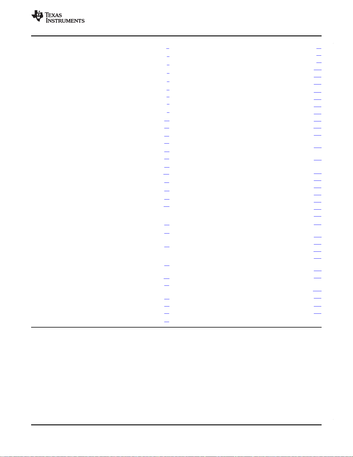
Figure 3-1. C674x Megamodule Block Diagram
12 Device Overview Copyright © 2009–2010, Texas Instruments Incorporated
Product Folder Link(s): TMS320C6748
Submit Documentation Feedback
Page 13

ADVANCEINFORMATION
TMS320C6748
www.ti.com
3.4.1 C674x DSP CPU Description
The C674x Central Processing Unit (CPU) consists of eight functional units, two register files, and two
data paths as shown in Figure 3-2. The two general-purpose register files (A and B) each contain
32 32-bit registers for a total of 64 registers. The general-purpose registers can be used for data or can be
data address pointers. The data types supported include packed 8-bit data, packed 16-bit data, 32-bit
data, 40-bit data, and 64-bit data. Values larger than 32 bits, such as 40-bit-long or 64-bit-long values are
stored in register pairs, with the 32 LSBs of data placed in an even register and the remaining 8 or
32 MSBs in the next upper register (which is always an odd-numbered register).
The eight functional units (.M1, .L1, .D1, .S1, .M2, .L2, .D2, and .S2) are each capable of executing one
instruction every clock cycle. The .M functional units perform all multiply operations. The .S and .L units
perform a general set of arithmetic, logical, and branch functions. The .D units primarily load data from
memory to the register file and store results from the register file into memory.
The C674x CPU combines the performance of the C64x+ core with the floating-point capabilities of the
C67x+ core.
Each C674x .M unit can perform one of the following each clock cycle: one 32 x 32 bit multiply, one 16 x
32 bit multiply, two 16 x 16 bit multiplies, two 16 x 32 bit multiplies, two 16 x 16 bit multiplies with
add/subtract capabilities, four 8 x 8 bit multiplies, four 8 x 8 bit multiplies with add operations, and four
16 x 16 multiplies with add/subtract capabilities (including a complex multiply). There is also support for
Galois field multiplication for 8-bit and 32-bit data. Many communications algorithms such as FFTs and
modems require complex multiplication. The complex multiply (CMPY) instruction takes for 16-bit inputs
and produces a 32-bit real and a 32-bit imaginary output. There are also complex multiplies with rounding
capability that produces one 32-bit packed output that contain 16-bit real and 16-bit imaginary values. The
32 x 32 bit multiply instructions provide the extended precision necessary for high-precision algorithms on
a variety of signed and unsigned 32-bit data types.
SPRS590B–JUNE 2009–REVISED AUGUST 2010
The .L or (Arithmetic Logic Unit) now incorporates the ability to do parallel add/subtract operations on a
pair of common inputs. Versions of this instruction exist to work on 32-bit data or on pairs of 16-bit data
performing dual 16-bit add and subtracts in parallel. There are also saturated forms of these instructions.
The C674x core enhances the .S unit in several ways. On the previous cores, dual 16-bit MIN2 and MAX2
comparisons were only available on the .L units. On the C674x core they are also available on the .S unit
which increases the performance of algorithms that do searching and sorting. Finally, to increase data
packing and unpacking throughput, the .S unit allows sustained high performance for the quad 8-bit/16-bit
and dual 16-bit instructions. Unpack instructions prepare 8-bit data for parallel 16-bit operations. Pack
instructions return parallel results to output precision including saturation support.
Other new features include:
• SPLOOP - A small instruction buffer in the CPU that aids in creation of software pipelining loops where
multiple iterations of a loop are executed in parallel. The SPLOOP buffer reduces the code size
associated with software pipelining. Furthermore, loops in the SPLOOP buffer are fully interruptible.
• Compact Instructions - The native instruction size for the C6000 devices is 32 bits. Many common
instructions such as MPY, AND, OR, ADD, and SUB can be expressed as 16 bits if the C674x
compiler can restrict the code to use certain registers in the register file. This compression is
performed by the code generation tools.
• Instruction Set Enhancement - As noted above, there are new instructions such as 32-bit
multiplications, complex multiplications, packing, sorting, bit manipulation, and 32-bit Galois field
multiplication.
• Exceptions Handling - Intended to aid the programmer in isolating bugs. The C674x CPU is able to
detect and respond to exceptions, both from internally detected sources (such as illegal op-codes) and
from system events (such as a watchdog time expiration).
• Privilege - Defines user and supervisor modes of operation, allowing the operating system to give a
basic level of protection to sensitive resources. Local memory is divided into multiple pages, each with
read, write, and execute permissions.
Copyright © 2009–2010, Texas Instruments Incorporated Device Overview 13
Submit Documentation Feedback
Product Folder Link(s): TMS320C6748
Page 14

ADVANCEINFORMATION
TMS320C6748
SPRS590B–JUNE 2009–REVISED AUGUST 2010
• Time-Stamp Counter - Primarily targeted for Real-Time Operating System (RTOS) robustness, a
free-running time-stamp counter is implemented in the CPU which is not sensitive to system stalls.
For more details on the C674x CPU and its enhancements over the C64x architecture, see the following
documents:
• TMS320C64x/C64x+ DSP CPU and Instruction Set Reference Guide (literature number SPRUFE8)
• TMS320C64x Technical Overview (literature number SPRU395)
www.ti.com
14 Device Overview Copyright © 2009–2010, Texas Instruments Incorporated
Submit Documentation Feedback
Product Folder Link(s): TMS320C6748
Page 15
ADVANCEINFORMATION
src2
src2
.D1
.M1
.S1
.L1
long src
odd dst
src2
src1
src1
src1
src1
even dst
even dst
odd dst
dst1
dst
src2
src2
src2
long src
DA1
ST1b
LD1b
LD1a
ST1a
Data path A
Odd
register
file A
(A1, A3,
A5...A31)
Odd
register
file B
(B1, B3,
B5...B31)
.D2
src1
dst
src2
DA2
LD2a
LD2b
src2
.M2
src1
dst1
.S2
src1
even dst
long src
odd dst
ST2a
ST2b
long src
.L2
even dst
odd dst
src1
Data path B
Control Register
32 MSB
32 LSB
dst2
(A)
32 MSB
32 LSB
2x
1x
32 LSB
32 MSB
32 LSB
32 MSB
dst2
(B)
(B)
(A)
8
8
8
8
32
32
32
32
(C)
(C)
Even
register
file A
(A0, A2,
A4...A30)
Even
register
file B
(B0, B2,
B4...B30)
(D)
(D)
(D)
(D)
A. On .M unit, dst2 is 32 MSB.
B. On .M unit, dst1 is 32 LSB.
C. On C64x CPU .M unit, src2 is 32 bits; on C64x+ CPU .M unit, src2 is 64 bits.
D. On .L and .S units, odd dst connects to odd register files and even dst connects to even register files.
TMS320C6748
www.ti.com
SPRS590B–JUNE 2009–REVISED AUGUST 2010
Figure 3-2. TMS320C674x CPU (DSP Core) Data Paths
Copyright © 2009–2010, Texas Instruments Incorporated Device Overview 15
Submit Documentation Feedback
Product Folder Link(s): TMS320C6748
Page 16
ADVANCEINFORMATION
TMS320C6748
SPRS590B–JUNE 2009–REVISED AUGUST 2010
3.4.2 DSP Memory Mapping
The DSP memory map is shown in .
By default the DSP also has access to most on and off chip memory areas.
Additionally, the DSP megamodule includes the capability to limit access to its internal memories through
its SDMA port; without needing an external MPU unit.
3.4.2.1 External Memories
The DSP has access to the following External memories:
• Asynchronous EMIF / SDRAM / NAND / NOR Flash (EMIFA)
• SDRAM (DDR2)
3.4.2.2 DSP Internal Memories
The DSP has access to the following DSP memories:
• L2 RAM
• L1P RAM
• L1D RAM
3.4.2.3 C674x CPU
The C674x core uses a two-level cache-based architecture. The Level 1 Program cache (L1P) is 32 KB
direct mapped cache and the Level 1 Data cache (L1D) is 32 KB 2-way set associated cache. The Level 2
memory/cache (L2) consists of a 256 KB memory space that is shared between program and data space.
L2 memory can be configured as mapped memory, cache, or a combination of both.
www.ti.com
Table 3-2 shows a memory map of the C674x CPU cache registers for the device.
Table 3-2. C674x Cache Registers
Byte Address Register Name Register Description
0x0184 0000 L2CFG L2 Cache configuration register
0x0184 0020 L1PCFG L1P Size Cache configuration register
0x0184 0024 L1PCC L1P Freeze Mode Cache configuration register
0x0184 0040 L1DCFG L1D Size Cache configuration register
0x0184 0044 L1DCC L1D Freeze Mode Cache configuration register
0x0184 0048 - 0x0184 0FFC - Reserved
0x0184 1000 EDMAWEIGHT L2 EDMA access control register
0x0184 1004 - 0x0184 1FFC - Reserved
0x0184 2000 L2ALLOC0 L2 allocation register 0
0x0184 2004 L2ALLOC1 L2 allocation register 1
0x0184 2008 L2ALLOC2 L2 allocation register 2
0x0184 200C L2ALLOC3 L2 allocation register 3
0x0184 2010 - 0x0184 3FFF - Reserved
0x0184 4000 L2WBAR L2 writeback base address register
0x0184 4004 L2WWC L2 writeback word count register
0x0184 4010 L2WIBAR L2 writeback invalidate base address register
0x0184 4014 L2WIWC L2 writeback invalidate word count register
0x0184 4018 L2IBAR L2 invalidate base address register
0x0184 401C L2IWC L2 invalidate word count register
0x0184 4020 L1PIBAR L1P invalidate base address register
0x0184 4024 L1PIWC L1P invalidate word count register
0x0184 4030 L1DWIBAR L1D writeback invalidate base address register
16 Device Overview Copyright © 2009–2010, Texas Instruments Incorporated
Submit Documentation Feedback
Product Folder Link(s): TMS320C6748
Page 17
ADVANCEINFORMATION
TMS320C6748
www.ti.com
SPRS590B–JUNE 2009–REVISED AUGUST 2010
Table 3-2. C674x Cache Registers (continued)
Byte Address Register Name Register Description
0x0184 4034 L1DWIWC L1D writeback invalidate word count register
0x0184 4038 - Reserved
0x0184 4040 L1DWBAR L1D Block Writeback
0x0184 4044 L1DWWC L1D Block Writeback
0x0184 4048 L1DIBAR L1D invalidate base address register
0x0184 404C L1DIWC L1D invalidate word count register
0x0184 4050 - 0x0184 4FFF - Reserved
0x0184 5000 L2WB L2 writeback all register
0x0184 5004 L2WBINV L2 writeback invalidate all register
0x0184 5008 L2INV L2 Global Invalidate without writeback
0x0184 500C - 0x0184 5027 - Reserved
0x0184 5028 L1PINV L1P Global Invalidate
0x0184 502C - 0x0184 5039 - Reserved
0x0184 5040 L1DWB L1D Global Writeback
0x0184 5044 L1DWBINV L1D Global Writeback with Invalidate
0x0184 5048 L1DINV L1D Global Invalidate without writeback
0x0184 8000 – 0x0184 80FF MAR0 - MAR63 Reserved 0x0000 0000 – 0x3FFF FFFF
0x0184 8100 – 0x0184 817F MAR64 – MAR95
0x0184 8180 – 0x0184 8187 MAR96 - MAR97
0x0184 8188 – 0x0184 818F MAR98 – MAR99
0x0184 8190 – 0x0184 8197 MAR100 – MAR101
0x0184 8198 – 0x0184 819F MAR102 – MAR103
0x0184 81A0 – 0x0184 81FF MAR104 – MAR127 Reserved 0x6800 0000 – 0x7FFF FFFF
0x0184 8200 MAR128
0x0184 8204 – 0x0184 82FF MAR129 – MAR191 Reserved 0x8200 0000 – 0xBFFF FFFF
0x0184 8300 – 0x0184 837F MAR192 – MAR223
0x0184 8380 – 0x0184 83FF MAR224 – MAR255 Reserved 0xE000 0000 – 0xFFFF FFFF
Memory Attribute Registers for EMIFA SDRAM Data (CS0)
External memory addresses 0x4000 0000 – 0x5FFF FFFF
Memory Attribute Registers for EMIFA Async Data (CS2)
External memory addresses 0x6000 0000 – 0x61FF FFFF
Memory Attribute Registers for EMIFA Async Data (CS3)
External memory addresses 0x6200 0000 – 0x63FF FFFF
Memory Attribute Registers for EMIFA Async Data (CS4)
External memory addresses 0x6400 0000 – 0x65FF FFFF
Memory Attribute Registers for EMIFA Async Data (CS5)
External memory addresses 0x6600 0000 – 0x67FF FFFF
Memory Attribute Register for RAM
External memory addresses 0x8000 0000 – 0x8001 FFFF
Reserved 0x8002 0000 – 0x81FF FFFF
Memory Attribute Registers for DDR2 Data (CS2)
External memory addresses 0xC000 0000 – 0xDFFF FFFF
Table 3-3. C674x L1/L2 Memory Protection Registers
HEX ADDRESS RANGE REGISTER ACRONYM DESCRIPTION
0x0184 A000 L2MPFAR L2 memory protection fault address register
0x0184 A004 L2MPFSR L2 memory protection fault status register
0x0184 A008 L2MPFCR L2 memory protection fault command register
0x0184 A00C - 0x0184 A0FF - Reserved
0x0184 A100 L2MPLK0 L2 memory protection lock key bits [31:0]
0x0184 A104 L2MPLK1 L2 memory protection lock key bits [63:32]
0x0184 A108 L2MPLK2 L2 memory protection lock key bits [95:64]
0x0184 A10C L2MPLK3 L2 memory protection lock key bits [127:96]
0x0184 A110 L2MPLKCMD L2 memory protection lock key command register
0x0184 A114 L2MPLKSTAT L2 memory protection lock key status register
0x0184 A118 - 0x0184 A1FF - Reserved
Copyright © 2009–2010, Texas Instruments Incorporated Device Overview 17
Submit Documentation Feedback
Product Folder Link(s): TMS320C6748
Page 18
ADVANCEINFORMATION
TMS320C6748
SPRS590B–JUNE 2009–REVISED AUGUST 2010
Table 3-3. C674x L1/L2 Memory Protection Registers (continued)
HEX ADDRESS RANGE REGISTER ACRONYM DESCRIPTION
0x0184 A200 L2MPPA0
0x0184 A204 L2MPPA1
0x0184 A208 L2MPPA2
0x0184 A20C L2MPPA3
0x0184 A210 L2MPPA4
0x0184 A214 L2MPPA5
0x0184 A218 L2MPPA6
0x0184 A21C L2MPPA7
0x0184 A220 L2MPPA8
0x0184 A224 L2MPPA9
0x0184 A228 L2MPPA10
0x0184 A22C L2MPPA11
0x0184 A230 L2MPPA12
0x0184 A234 L2MPPA13
0x0184 A238 L2MPPA14
0x0184 A23C L2MPPA15
0x0184 A240 L2MPPA16
0x0184 A244 L2MPPA17
0x0184 A248 L2MPPA18
0x0184 A24C L2MPPA19
0x0184 A250 L2MPPA20
0x0184 A254 L2MPPA21
0x0184 A258 L2MPPA22
0x0184 A25C L2MPPA23
0x0184 A260 L2MPPA24
0x0184 A264 L2MPPA25
0x0184 A268 L2MPPA26
0x0184 A26C L2MPPA27
L2 memory protection page attribute register 0 (controls memory address
0x0080 0000 - 0x0080 1FFF)
L2 memory protection page attribute register 1 (controls memory address
0x0080 2000 - 0x0080 3FFF)
L2 memory protection page attribute register 2 (controls memory address
0x0080 4000 - 0x0080 5FFF)
L2 memory protection page attribute register 3 (controls memory address
0x0080 6000 - 0x0080 7FFF)
L2 memory protection page attribute register 4 (controls memory address
0x0080 8000 - 0x0080 9FFF)
L2 memory protection page attribute register 5 (controls memory address
0x0080 A000 - 0x0080 BFFF)
L2 memory protection page attribute register 6 (controls memory address
0x0080 C000 - 0x0080 DFFF)
L2 memory protection page attribute register 7 (controls memory address
0x0080 E000 - 0x0080 FFFF)
L2 memory protection page attribute register 8 (controls memory address
0x0081 0000 - 0x0081 1FFF)
L2 memory protection page attribute register 9 (controls memory address
0x0081 2000 - 0x0081 3FFF)
L2 memory protection page attribute register 10 (controls memory address
0x0081 4000 - 0x0081 5FFF)
L2 memory protection page attribute register 11 (controls memory address
0x0081 6000 - 0x0081 7FFF)
L2 memory protection page attribute register 12 (controls memory address
0x0081 8000 - 0x0081 9FFF)
L2 memory protection page attribute register 13 (controls memory address
0x0081 A000 - 0x0081 BFFF)
L2 memory protection page attribute register 14 (controls memory address
0x0081 C000 - 0x0081 DFFF)
L2 memory protection page attribute register 15 (controls memory address
0x0081 E000 - 0x0081 FFFF)
L2 memory protection page attribute register 16 (controls memory address
0x0082 0000 - 0x0082 1FFF)
L2 memory protection page attribute register 17 (controls memory address
0x0082 2000 - 0x0082 3FFF)
L2 memory protection page attribute register 18 (controls memory address
0x0082 4000 - 0x0082 5FFF)
L2 memory protection page attribute register 19 (controls memory address
0x0082 6000 - 0x0082 7FFF)
L2 memory protection page attribute register 20 (controls memory address
0x0082 8000 - 0x0082 9FFF)
L2 memory protection page attribute register 21 (controls memory address
0x0082 A000 - 0x0082 BFFF)
L2 memory protection page attribute register 22 (controls memory address
0x0082 C000 - 0x0082 DFFF)
L2 memory protection page attribute register 23 (controls memory address
0x0082 E000 - 0x0082 FFFF)
L2 memory protection page attribute register 24 (controls memory address
0x0083 0000 - 0x0083 1FFF)
L2 memory protection page attribute register 25 (controls memory address
0x0083 2000 - 0x0083 3FFF)
L2 memory protection page attribute register 26 (controls memory address
0x0083 4000 - 0x0083 5FFF)
L2 memory protection page attribute register 27 (controls memory address
0x0083 6000 - 0x0083 7FFF)
www.ti.com
18 Device Overview Copyright © 2009–2010, Texas Instruments Incorporated
Submit Documentation Feedback
Product Folder Link(s): TMS320C6748
Page 19
ADVANCEINFORMATION
TMS320C6748
www.ti.com
SPRS590B–JUNE 2009–REVISED AUGUST 2010
Table 3-3. C674x L1/L2 Memory Protection Registers (continued)
HEX ADDRESS RANGE REGISTER ACRONYM DESCRIPTION
0x0184 A270 L2MPPA28
0x0184 A274 L2MPPA29
0x0184 A278 L2MPPA30
0x0184 A27C L2MPPA31
0x0184 A280 L2MPPA32
0x0184 A284 L2MPPA33
0x0184 A288 L2MPPA34
0x0184 A28C L2MPPA35
0x0184 A290 L2MPPA36
0x0184 A294 L2MPPA37
0x0184 A298 L2MPPA38
0x0184 A29C L2MPPA39
0x0184 A2A0 L2MPPA40
0x0184 A2A4 L2MPPA41
0x0184 A2A8 L2MPPA42
0x0184 A2AC L2MPPA43
0x0184 A2B0 L2MPPA44
0x0184 A2B4 L2MPPA45
0x0184 A2B8 L2MPPA46
0x0184 A2BC L2MPPA47
0x0184 A2C0 L2MPPA48
0x0184 A2C4 L2MPPA49
0x0184 A2C8 L2MPPA50
0x0184 A2CC L2MPPA51
0x0184 A2D0 L2MPPA52
0x0184 A2D4 L2MPPA53
0x0184 A2D8 L2MPPA54
0x0184 A2DC L2MPPA55
L2 memory protection page attribute register 28 (controls memory address
0x0083 8000 - 0x0083 9FFF)
L2 memory protection page attribute register 29 (controls memory address
0x0083 A000 - 0x0083 BFFF)
L2 memory protection page attribute register 30 (controls memory address
0x0083 C000 - 0x0083 DFFF)
L2 memory protection page attribute register 31 (controls memory address
0x0083 E000 - 0x0083 FFFF)
L2 memory protection page attribute register 32 (controls memory address
0x0070 0000 - 0x0070 7FFF)
L2 memory protection page attribute register 33 (controls memory address
0x0070 8000 - 0x0070 FFFF)
L2 memory protection page attribute register 34 (controls memory address
0x0071 0000 - 0x0071 7FFF)
L2 memory protection page attribute register 35 (controls memory address
0x0071 8000 - 0x0071 FFFF)
L2 memory protection page attribute register 36 (controls memory address
0x0072 0000 - 0x0072 7FFF)
L2 memory protection page attribute register 37 (controls memory address
0x0072 8000 - 0x0072 FFFF)
L2 memory protection page attribute register 38 (controls memory address
0x0073 0000 - 0x0073 7FFF)
L2 memory protection page attribute register 39 (controls memory address
0x0073 8000 - 0x0073 FFFF)
L2 memory protection page attribute register 40 (controls memory address
0x0074 0000 - 0x0074 7FFF)
L2 memory protection page attribute register 41 (controls memory address
0x0074 8000 - 0x0074 FFFF)
L2 memory protection page attribute register 42 (controls memory address
0x0075 0000 - 0x0075 7FFF)
L2 memory protection page attribute register 43 (controls memory address
0x0075 8000 - 0x0075 FFFF)
L2 memory protection page attribute register 44 (controls memory address
0x0076 0000 - 0x0076 7FFF)
L2 memory protection page attribute register 45 (controls memory address
0x0076 8000 - 0x0076 FFFF)
L2 memory protection page attribute register 46 (controls memory address
0x0077 0000 - 0x0077 7FFF)
L2 memory protection page attribute register 47 (controls memory address
0x0077 8000 - 0x0077 FFFF)
L2 memory protection page attribute register 48 (controls memory address
0x0078 0000 - 0x0078 7FFF)
L2 memory protection page attribute register 49 (controls memory address
0x0078 8000 - 0x0078 FFFF)
L2 memory protection page attribute register 50 (controls memory address
0x0079 0000 - 0x0079 7FFF)
L2 memory protection page attribute register 51 (controls memory address
0x0079 8000 - 0x0079 FFFF)
L2 memory protection page attribute register 52 (controls memory address
0x007A 0000 - 0x007A 7FFF)
L2 memory protection page attribute register 53 (controls memory address
0x007A 8000 - 0x007A FFFF)
L2 memory protection page attribute register 54 (controls memory address
0x007B 0000 - 0x007B 7FFF)
L2 memory protection page attribute register 55 (controls memory address
0x007B 8000 - 0x007B FFFF)
Copyright © 2009–2010, Texas Instruments Incorporated Device Overview 19
Submit Documentation Feedback
Product Folder Link(s): TMS320C6748
Page 20
ADVANCEINFORMATION
TMS320C6748
SPRS590B–JUNE 2009–REVISED AUGUST 2010
Table 3-3. C674x L1/L2 Memory Protection Registers (continued)
HEX ADDRESS RANGE REGISTER ACRONYM DESCRIPTION
0x0184 A2E0 L2MPPA56
0x0184 A2E4 L2MPPA57
0x0184 A2E8 L2MPPA58
0x0184 A2EC L2MPPA59
0x0184 A2F0 L2MPPA60
0x0184 A2F4 L2MPPA61
0x0184 A2F8 L2MPPA62
0x0184 A2FC L2MPPA63
0x0184 A300 - 0x0184 A3FF - Reserved
0x0184 A400 L1PMPFAR L1P memory protection fault address register
0x0184 A404 L1PMPFSR L1P memory protection fault status register
0x0184 A408 L1PMPFCR L1P memory protection fault command register
0x0184 A40C - 0x0184 A4FF - Reserved
0x0184 A500 L1PMPLK0 L1P memory protection lock key bits [31:0]
0x0184 A504 L1PMPLK1 L1P memory protection lock key bits [63:32]
0x0184 A508 L1PMPLK2 L1P memory protection lock key bits [95:64]
0x0184 A50C L1PMPLK3 L1P memory protection lock key bits [127:96]
0x0184 A510 L1PMPLKCMD L1P memory protection lock key command register
0x0184 A514 L1PMPLKSTAT L1P memory protection lock key status register
0x0184 A518 - 0x0184 A5FF - Reserved
0x0184 A600 - 0x0184 A63F - Reserved
0x0184 A640 L1PMPPA16
0x0184 A644 L1PMPPA17
0x0184 A648 L1PMPPA18
0x0184 A64C L1PMPPA19
0x0184 A650 L1PMPPA20
0x0184 A654 L1PMPPA21
0x0184 A658 L1PMPPA22
0x0184 A65C L1PMPPA23
0x0184 A660 L1PMPPA24
0x0184 A664 L1PMPPA25
0x0184 A668 L1PMPPA26
L2 memory protection page attribute register 56 (controls memory address
0x007C 0000 - 0x007C 7FFF)
L2 memory protection page attribute register 57 (controls memory address
0x007C 8000 - 0x007C FFFF)
L2 memory protection page attribute register 58 (controls memory address
0x007D 0000 - 0x007D 7FFF)
L2 memory protection page attribute register 59 (controls memory address
0x007D 8000 - 0x007D FFFF)
L2 memory protection page attribute register 60 (controls memory address
0x007E 0000 - 0x007E 7FFF)
L2 memory protection page attribute register 61 (controls memory address
0x007E 8000 - 0x007E FFFF)
L2 memory protection page attribute register 62 (controls memory address
0x007F 0000 - 0x007F 7FFF)
L2 memory protection page attribute register 63 (controls memory address
0x007F 8000 - 0x007F FFFF)
(1)
L1P memory protection page attribute register 16 (controls memory address
0x00E0 0000 - 0x00E0 07FF)
L1P memory protection page attribute register 17 (controls memory address
0x00E0 0800 - 0x00E0 0FFF)
L1P memory protection page attribute register 18 (controls memory address
0x00E0 1000 - 0x00E0 17FF)
L1P memory protection page attribute register 19 (controls memory address
0x00E0 1800 - 0x00E0 1FFF)
L1P memory protection page attribute register 20 (controls memory address
0x00E0 2000 - 0x00E0 27FF)
L1P memory protection page attribute register 21 (controls memory address
0x00E0 2800 - 0x00E0 2FFF)
L1P memory protection page attribute register 22 (controls memory address
0x00E0 3000 - 0x00E0 37FF)
L1P memory protection page attribute register 23 (controls memory address
0x00E0 3800 - 0x00E0 3FFF)
L1P memory protection page attribute register 24 (controls memory address
0x00E0 4000 - 0x00E0 47FF)
L1P memory protection page attribute register 25 (controls memory address
0x00E0 4800 - 0x00E0 4FFF)
L1P memory protection page attribute register 26 (controls memory address
0x00E0 5000 - 0x00E0 57FF)
www.ti.com
(1) These addresses correspond to the L1P memory protection page attribute registers 0-15 (L1PMPPA0-L1PMPPA15) of the C674x
megamaodule. These registers are not supported for this device.
20 Device Overview Copyright © 2009–2010, Texas Instruments Incorporated
Submit Documentation Feedback
Product Folder Link(s): TMS320C6748
Page 21
ADVANCEINFORMATION
TMS320C6748
www.ti.com
SPRS590B–JUNE 2009–REVISED AUGUST 2010
Table 3-3. C674x L1/L2 Memory Protection Registers (continued)
HEX ADDRESS RANGE REGISTER ACRONYM DESCRIPTION
0x0184 A66C L1PMPPA27
0x0184 A670 L1PMPPA28
0x0184 A674 L1PMPPA29
0x0184 A678 L1PMPPA30
0x0184 A67C L1PMPPA31
0x0184 A67F – 0x0184 ABFF - Reserved
0x0184 AC00 L1DMPFAR L1D memory protection fault address register
0x0184 AC04 L1DMPFSR L1D memory protection fault status register
0x0184 AC08 L1DMPFCR L1D memory protection fault command register
0x0184 AC0C - 0x0184 ACFF - Reserved
0x0184 AD00 L1DMPLK0 L1D memory protection lock key bits [31:0]
0x0184 AD04 L1DMPLK1 L1D memory protection lock key bits [63:32]
0x0184 AD08 L1DMPLK2 L1D memory protection lock key bits [95:64]
0x0184 AD0C L1DMPLK3 L1D memory protection lock key bits [127:96]
0x0184 AD10 L1DMPLKCMD L1D memory protection lock key command register
0x0184 AD14 L1DMPLKSTAT L1D memory protection lock key status register
0x0184 AD18 - 0x0184 ADFF - Reserved
0x0184 AE00 - 0x0184 AE3F - Reserved
0x0184 AE40 L1DMPPA16
0x0184 AE44 L1DMPPA17
0x0184 AE48 L1DMPPA18
0x0184 AE4C L1DMPPA19
0x0184 AE50 L1DMPPA20
0x0184 AE54 L1DMPPA21
0x0184 AE58 L1DMPPA22
0x0184 AE5C L1DMPPA23
0x0184 AE60 L1DMPPA24
0x0184 AE64 L1DMPPA25
0x0184 AE68 L1DMPPA26
0x0184 AE6C L1DMPPA27
0x0184 AE70 L1DMPPA28
0x0184 AE74 L1DMPPA29
L1P memory protection page attribute register 27 (controls memory address
0x00E0 5800 - 0x00E0 5FFF)
L1P memory protection page attribute register 28 (controls memory address
0x00E0 6000 - 0x00E0 67FF)
L1P memory protection page attribute register 29 (controls memory address
0x00E0 6800 - 0x00E0 6FFF)
L1P memory protection page attribute register 30 (controls memory address
0x00E0 7000 - 0x00E0 77FF)
L1P memory protection page attribute register 31 (controls memory address
0x00E0 7800 - 0x00E0 7FFF)
(2)
L1D memory protection page attribute register 16 (controls memory address
0x00F0 0000 - 0x00F0 07FF)
L1D memory protection page attribute register 17 (controls memory address
0x00F0 0800 - 0x00F0 0FFF)
L1D memory protection page attribute register 18 (controls memory address
0x00F0 1000 - 0x00F0 17FF)
L1D memory protection page attribute register 19 (controls memory address
0x00F0 1800 - 0x00F0 1FFF)
L1D memory protection page attribute register 20 (controls memory address
0x00F0 2000 - 0x00F0 27FF)
L1D memory protection page attribute register 21 (controls memory address
0x00F0 2800 - 0x00F0 2FFF)
L1D memory protection page attribute register 22 (controls memory address
0x00F0 3000 - 0x00F0 37FF)
L1D memory protection page attribute register 23 (controls memory address
0x00F0 3800 - 0x00F0 3FFF)
L1D memory protection page attribute register 24 (controls memory address
0x00F0 4000 - 0x00F0 47FF)
L1D memory protection page attribute register 25 (controls memory address
0x00F0 4800 - 0x00F0 4FFF)
L1D memory protection page attribute register 26 (controls memory address
0x00F0 5000 - 0x00F0 57FF)
L1D memory protection page attribute register 27 (controls memory address
0x00F0 5800 - 0x00F0 5FFF)
L1D memory protection page attribute register 28 (controls memory address
0x00F0 6000 - 0x00F0 67FF)
L1D memory protection page attribute register 29 (controls memory address
0x00F0 6800 - 0x00F0 6FFF)
(2) These addresses correspond to the L1D memory protection page attribute registers 0-15 (L1DMPPA0-L1DMPPA15) of the C674x
megamaodule. These registers are not supported for this device.
Copyright © 2009–2010, Texas Instruments Incorporated Device Overview 21
Submit Documentation Feedback
Product Folder Link(s): TMS320C6748
Page 22

ADVANCEINFORMATION
TMS320C6748
SPRS590B–JUNE 2009–REVISED AUGUST 2010
Table 3-3. C674x L1/L2 Memory Protection Registers (continued)
HEX ADDRESS RANGE REGISTER ACRONYM DESCRIPTION
0x0184 AE78 L1DMPPA30
0x0184 AE7C L1DMPPA31
0x0184 AE80 – 0x0185 FFFF - Reserved
L1D memory protection page attribute register 30 (controls memory address
0x00F0 7000 - 0x00F0 77FF)
L1D memory protection page attribute register 31 (controls memory address
0x00F0 7800 - 0x00F0 7FFF)
www.ti.com
22 Device Overview Copyright © 2009–2010, Texas Instruments Incorporated
Submit Documentation Feedback
Product Folder Link(s): TMS320C6748
Page 23
ADVANCEINFORMATION
TMS320C6748
www.ti.com
SPRS590B–JUNE 2009–REVISED AUGUST 2010
3.5 Memory Map Summary
Table 3-4. C6748 Top Level Memory Map
Start End Size DSP Mem Map EDMA Mem Map PRUSS Mem Master LCDC
Address Address Map Peripheral Mem
0x0000 0000 0x0000 0FFF 4K PRUSS Local -
0x0000 1000 0x006F FFFF 0x0070 0000 0x007F FFFF 1024K DSP L2 ROM
0x0080 0000 0x0083 FFFF 256K DSP L2 RAM
0x0084 0000 0x00DF
FFFF
0x00E0 0000 0x00E0 7FFF 32K DSP L1P RAM
0x00E0 8000 0x00EF
FFFF
0x00F0 0000 0x00F0 7FFF 32K DSP L1D RAM
0x00F0 8000 0x017F FFFF
0x0180 0000 0x0180 FFFF 64K DSP Interrupt Controller
0x0181 0000 0x0181 0FFF 4K DSP Powerdown Controller
0x0181 1000 0x0181 1FFF 4K DSP Security ID
0x0181 2000 0x0181 2FFF 4K DSP Revision ID
0x0181 3000 0x0181 FFFF 52K 0x0182 0000 0x0182 FFFF 64K DSP EMC
0x0183 0000 0x0183 FFFF 64K DSP Internal Reserved
0x0184 0000 0x0184 FFFF 64K DSP Memory System
0x0185 0000 0x01BB
FFFF
0x01BC 0000 0x01BC 4K
0FFF
0x01BC 1000 0x01BC 2K
17FF
0x01BC 1800 0x01BC 256
18FF
0x01BC 1900 0x01BF
FFFF
0x01C0 0000 0x01C0 7FFF 32K EDMA3 CC
0x01C0 8000 0x01C0 83FF 1K EDMA3 TC0
0x01C0 8400 0x01C0 87FF 1K EDMA3 TC1
0x01C0 8800 0x01C0
FFFF
0x01C1 0000 0x01C1 0FFF 4K PSC 0
0x01C1 1000 0x01C1 1FFF 4K PLL Controller 0
0x01C1 2000 0x01C1 3FFF
0x01C1 4000 0x01C1 4FFF 4K SYSCFG0
0x01C1 5000 0x01C1
FFFF
0x01C2 0000 0x01C2 0FFF 4K Timer0
0x01C2 1000 0x01C2 1FFF 4K Timer1
0x01C2 2000 0x01C2 2FFF 4K I2C 0
0x01C2 3000 0x01C2 3FFF 4K RTC
(1)
Address
Space
Mem Map Map
(1) The DSP L2 ROM is used for boot purposes and cannot be programmed with application code
Copyright © 2009–2010, Texas Instruments Incorporated Device Overview 23
Submit Documentation Feedback
Product Folder Link(s): TMS320C6748
Page 24
ADVANCEINFORMATION
TMS320C6748
SPRS590B–JUNE 2009–REVISED AUGUST 2010
www.ti.com
Table 3-4. C6748 Top Level Memory Map (continued)
Start End Size DSP Mem Map EDMA Mem Map PRUSS Mem Master LCDC
Address Address Map Peripheral Mem
0x01C2 4000 0x01C3
FFFF
0x01C4 0000 0x01C4 0FFF 4K MMC/SD 0
0x01C4 1000 0x01C4 1FFF 4K SPI 0
0x01C4 2000 0x01C4 2FFF 4K UART 0
0x01C4 3000 0x01CF
FFFF
0x01D0 0000 0x01D0 0FFF 4K McASP 0 Control
0x01D0 1000 0x01D0 1FFF 4K McASP 0 AFIFO Ctrl
0x01D0 2000 0x01D0 2FFF 4K McASP 0 Data
0x01D0 3000 0x01D0
BFFF
0x01D0 C000 0x01D0 4K UART 1
CFFF
0x01D0 D000 0x01D0 4K UART 2
DFFF
0x01D0 E000 0x01D0
FFFF
0x01D1 0000 0x01D1 07FF 2K McBSP0
0x01D1 0800 0x01D1 0FFF 2K McBSP0 FIFO Ctrl
0x01D1 1000 0x01D1 17FF 2K McBSP1
0x01D1 1800 0x01D1 1FFF 2K McBSP1 FIFO Ctrl
0x01D1 2000 0x01DF
FFFF
0x01E0 0000 0x01E0 FFFF 64K USB0
0x01E1 0000 0x01E1 0FFF 4K UHPI
0x01E1 1000 0x01E1 2FFF
0x01E1 3000 0x01E1 3FFF 4K LCD Controller
0x01E1 4000 0x01E1 4FFF 4K Memory Protection Unit 1 (MPU 1)
0x01E1 5000 0x01E1 5FFF 4K Memory Protection Unit 2 (MPU 2)
0x01E1 6000 0x01E1 6FFF 4K UPP
0x01E1 7000 0x01E1 7FFF 4K VPIF
0x01E1 8000 0x01E1 9FFF 8K SATA
0x01E1 A000 0x01E1 4K PLL Controller 1
AFFF
0x01E1 B000 0x01E1 4K MMCSD1
BFFF
0x01E1 C000 0x01E1 FFFF
0x01E2 0000 0x01E2 1FFF 8K EMAC Control Module RAM
0x01E2 2000 0x01E2 2FFF 4K EMAC Control Module Registers
0x01E2 3000 0x01E2 3FFF 4K EMAC Control Registers
0x01E2 4000 0x01E2 4FFF 4K EMAC MDIO port
0x01E2 5000 0x01E2 5FFF 4K USB1
0x01E2 6000 0x01E2 6FFF 4K GPIO
0x01E2 7000 0x01E2 7FFF 4K PSC 1
0x01E2 8000 0x01E2 8FFF 4K I2C 1
0x01E2 9000 0x01E2
BFFF
Mem Map Map
24 Device Overview Copyright © 2009–2010, Texas Instruments Incorporated
Submit Documentation Feedback
Product Folder Link(s): TMS320C6748
Page 25
ADVANCEINFORMATION
TMS320C6748
www.ti.com
SPRS590B–JUNE 2009–REVISED AUGUST 2010
Table 3-4. C6748 Top Level Memory Map (continued)
Start End Size DSP Mem Map EDMA Mem Map PRUSS Mem Master LCDC
Address Address Map Peripheral Mem
0x01E2 C000 0x01E2 4K SYSCFG1
0x01E2 D000 0x01E2 FFFF
0x01E3 0000 0x01E3 7FFF 32K EDMA3 CC1
0x01E3 8000 0x01E3 83FF 1K EDMA3 TC2
0x01E3 8400 0x01EF
0x01F0 0000 0x01F0 0FFF 4K eHRPWM 0
0x01F0 1000 0x01F0 1FFF 4K HRPWM 0
0x01F0 2000 0x01F0 2FFF 4K eHRPWM 1
0x01F0 3000 0x01F0 3FFF 4K HRPWM 1
0x01F0 4000 0x01F0 5FFF
0x01F0 6000 0x01F0 6FFF 4K ECAP 0
0x01F0 7000 0x01F0 7FFF 4K ECAP 1
0x01F0 8000 0x01F0 8FFF 4K ECAP 2
0x01F0 9000 0x01F0 BFFF
0x01F0 C000 0x01F0 4K Timer2
0x01F0 D000 0x01F0 4K Timer3
0x01F0 E000 0x01F0 EFFF 4K SPI1
0x01F0 F000 0x01F0 FFFF
0x01F1 0000 0x01F1 0FFF 4K McBSP0 FIFO Data
0x01F1 1000 0x01F1 1FFF 4K McBSP1 FIFO Data
0x01F1 2000 0x116F FFFF
0x1170 0000 0x117F FFFF 1024K DSP L2 ROM
0x1180 0000 0x1183 FFFF 256K DSP L2 RAM
0x1184 0000 0x11DF
0x11E0 0000 0x11E0 7FFF 32K DSP L1P RAM
0x11E0 8000 0x11EF
0x11F0 0000 0x11F0 7FFF 32K DSP L1D RAM
0x11F0 8000 0x3FFF
0x4000 0000 0x5FFF 512M EMIFA SDRAM data (CS0)
0x6000 0000 0x61FF FFFF 32M EMIFA async data (CS2)
0x6200 0000 0x63FF FFFF 32M EMIFA async data (CS3)
0x6400 0000 0x65FF FFFF 32M EMIFA async data (CS4)
0x6600 0000 0x67FF FFFF 32M EMIFA async data (CS5)
0x6800 0000 0x6800 7FFF 32K EMIFA Control Regs
0x6800 8000 0x7FFF
0x8000 0000 0x8001 FFFF 128K On-chip RAM
0x8002 0000 0xAFFF
0xB000 0000 0xB000 7FFF 32K DDR2 Control Regs
CFFF
FFFF
CFFF
DFFF
(2)
FFFF
FFFF
FFFF
FFFF
FFFF
FFFF
Mem Map Map
(2) The DSP L2 ROM is used for boot purposes and cannot be programmed with application code
Copyright © 2009–2010, Texas Instruments Incorporated Device Overview 25
Submit Documentation Feedback
Product Folder Link(s): TMS320C6748
Page 26
ADVANCEINFORMATION
TMS320C6748
SPRS590B–JUNE 2009–REVISED AUGUST 2010
www.ti.com
Table 3-4. C6748 Top Level Memory Map (continued)
Start End Size DSP Mem Map EDMA Mem Map PRUSS Mem Master LCDC
Address Address Map Peripheral Mem
0xB000 8000 0xBFFF
FFFF
0xC000 0000 0xDFFF 512M DDR2 Data
FFFF
0xE000 0000 0xFFFC
FFFF
0xFFFD 0000 0xFFFD 64K
FFFF
0xFFFE 0000 0xFFFE
DFFF
0xFFFE 0xFFFE 8K
E000 FFFF
0xFFFF 0000 0xFFFF 8K
1FFF
0xFFFF 2000 0xFFFF
FFFF
Mem Map Map
26 Device Overview Copyright © 2009–2010, Texas Instruments Incorporated
Submit Documentation Feedback
Product Folder Link(s): TMS320C6748
Page 27
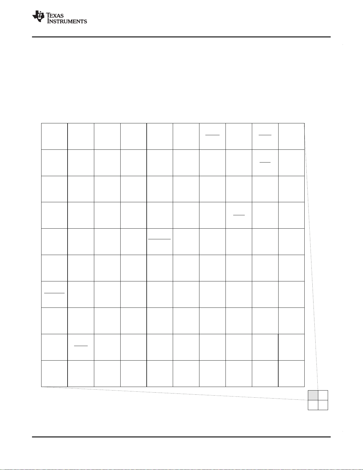
ADVANCEINFORMATION
W
V
U
T
R
P
N
M
L
K
10987654321
10987654321
DVDD3318_C
VP_CLKOUT3/
PRU1_R30[0]/
GP6[1]/
PRU1_R31[1]
SATA_VSS
SATA_RXP
VP_CLKOUT2/
MMCSD1_DAT[2]/
PRU1_R30[2]/
GP6[3]/
PRU1_R31[3]
SATA_RXN
SATA_VDD
SATA_REFCLKN
SATA_REGSATA_REFCLKP SATA_VDD
SATA_VDD SATA_VDDRSATA_VDD
DVDD3318_C
DDR_A[11]
VP_DOUT[15]/
LCD_D[15]/
UPP_XD[7]/
GP7[7]/
BOOT[7]
DV
DD3318_C
DV
DD18
DDR_DVDD18 DDR_DVDD18
DDR_D[15]
DDR_RAS
DDR_CLKPDDR_CLKN
DDR_A[2]DDR_A[10]
V
SS
LCD_AC_ENB_CS/
GP6[0]/
PRU1_R31[28]
DDR_A[13]
DDR_CAS
DDR_A[5]
DDR_CKE
DDR_BA[0]
V
SS
CV
DD
RV
DD
DDR_A[9] DDR_A[1]
DDR_WE
DDR_D[10]
DDR_A[7]
DDR_A[0] DDR_D[12]
DDR_A[12]
DDR_A[3]
DDR_CS
DDR_A[6]
DDR_DQM[1]
SATA_VSS
CV
DD
SATA_VSS
DDR_DVDD18
VP_DOUT[12]/
LCD_D[12]/
UPP_XD[4]/
GP7[4]/
BOOT[4]
DDR_VREF
DDR_BA[1]
DDR_A[8]
DDR_A[4]
DDR_BA[2]
SATA_VSS
W
V
U
T
R
P
N
M
L
K
DDR_D[13]
V
SS
V
SS
V
SS
V
SS
DV
DD18
V
SS
V
SS
V
SS
V
SS
NC
V
SS
V
SS
V
SS
V
SS
CV
DD
CV
DD
V
SS
DDR_DVDD18DDR_DVDD18DDR_DVDD18DDR_DVDD18
DVDD3318_C
VP_DOUT[13]/
LCD_D[13]/
UPP_XD[5]/
GP7[5]/
BOOT[5]
VP_DOUT[14]/
LCD_D[14]/
UPP_XD[6]/
GP7[6]/
BOOT[6]
DDR_DVDD18 DDR_DVDD18 DDR_DVDD18
VP_DOUT[9]/
LCD_D[9]/
UPP_XD[1]/
GP7[1]/
BOOT[1]
VP_DOUT[10]/
LCD_D[10]/
UPP_XD[2]/
GP7[2]/
BOOT[2]
VP_DOUT[11]/
LCD_D[11]/
UPP_XD[3]/
GP7[3]/
BOOT[3]
VP_DOUT[6]/
LCD_D[6]/
UPP_XD[14]/
GP7[14]/
PRU1_R31[14]
VP_DOUT[7]/
LCD_D[7]/
UPP_XD[15]/
GP7[15]/
PRU1_R31[15]
VP_DOUT[8]/
LCD_D[8]/
UPP_XD[0]/
GP7[0]/
BOOT[0]
VP_DOUT[3]/
LCD_D[3]/
UPP_XD[11]/
GP7[11]/
PRU1_R31[11]
VP_DOUT[4]/
LCD_D[4]/
UPP_XD[12]/
GP7[12]/
PRU1_R31[12]
VP_DOUT[5]/
LCD_D[5]/
UPP_XD[13]/
GP7[13]/
PRU1_R31[13]
VP_DOUT[0]/
LCD_D[0]/
UPP_XD[8]/
GP7[8]/
PRU1_R31[8]
VP_DOUT[1]/
LCD_D[1]/
UPP_XD[9]/
GP7[9]/
PRU1_R31[9]
VP_DOUT[2]/
LCD_D[2]/
UPP_XD[10]/
GP7[10]/
PRU1_R31[10]
TMS320C6748
www.ti.com
SPRS590B–JUNE 2009–REVISED AUGUST 2010
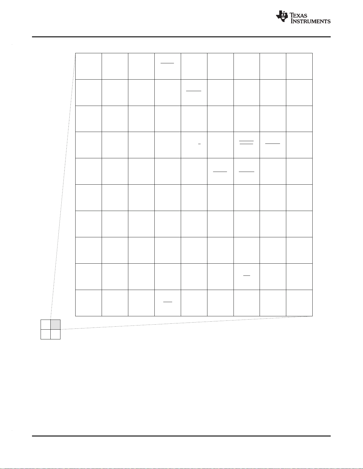
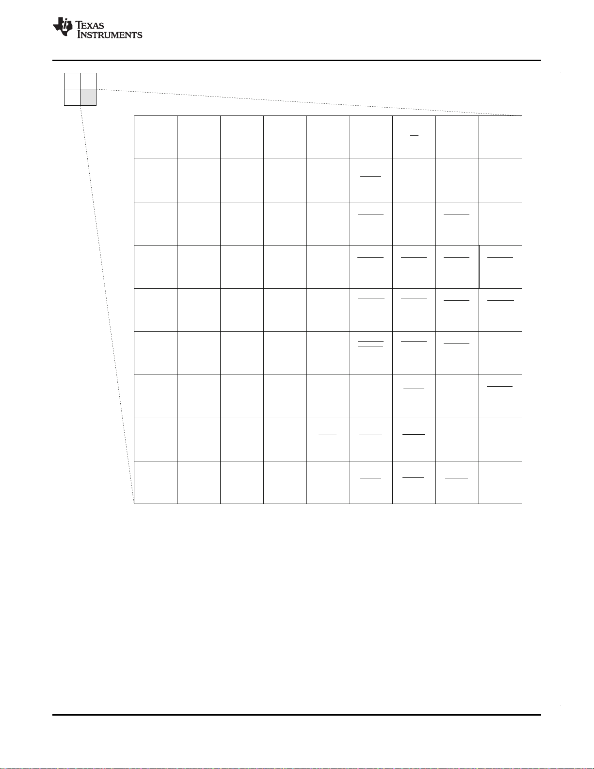
3.6 Pin Assignments
Extensive use of pin multiplexing is used to accommodate the largest number of peripheral functions in
the smallest possible package. Pin multiplexing is controlled using a combination of hardware
configuration at device reset and software programmable register settings.
3.6.1 Pin Map (Bottom View)
The following graphics show the bottom view of the ZCE and ZWT packages pin assignments in four
quadrants (A, B, C, and D). The pin assignments for both packages are identical.
Figure 3-3. Pin Map (Quad A)
Copyright © 2009–2010, Texas Instruments Incorporated Device Overview 27
Submit Documentation Feedback
Product Folder Link(s): TMS320C6748
Page 28
ADVANCEINFORMATION
W
V
U
T
R
P
N
M
L
K
191817161514131211
191817161514131211
USB1_VDD33
DVDD3318_C
CV
DD
USB_CVDD
DVDD3318_C
DDR_DQGATE0
DVDD18
DDR_DQGATE1
DDR_D[9] DDR_D[8]DDR_D[11]
DVDD18
RTC_CVDD
RESET
USB0_DM USB0_DP
VP_DIN[11]/
UHPI_HD[3]/
UPP_D[3]/
PRU0_R30[11]/
PRU0_R31[11]
USB0_VDDA33 USB0_VBUS
USB1_DM
VP_DIN[0]/
UHPI_HD[8]/
UPP_D[8]/
RMII_CRS_DV/
PRU1_R31[29]
VP_DIN[1]/
UHPI_HD[9]/
UPP_D[9]/
RMII_MHZ_50_CLK/
PRU0_R31[23]
VP_DIN[2]/
UHPI_HD[10]/
UPP_D[10]/
RMII_RXER/
PRU0_R31[24]
VP_DIN[4]/
UHPI_HD[12]/
UPP_D[12]/
RMII_RXD[1]/
PRU0_R31[26]
PRU0_R30[28]/
UHPI_HCNTL1/
UPP_CHA_START/
GP6[10]
USB1_DP
PLL0_VDDA
PRU0_R30[30]/
/
PRU1_R30[11]/
GP6[12]
UHPI_HINT
USB0_VDDA18
VP_DIN[5]/
UHPI_HD[13]/
UPP_D[13]/
RMII_TXEN/
PRU0_R31[27]
DDR_D[1]
VP_DIN[7]/
UHPI_HD[15]/
UPP_D[15]/
RMII_TXD[1]/
PRU0_R31[29]
OSCVSS
DDR_D[2]
VP_DIN[6]/
UHPI_HD[14]/
UPP_D[14]/
RMII_TXD[0]/
PRU0_R31[28]
VP_DIN[3]/
UHPI_HD[11]/
UPP_D[11]/
RMII_RXD[0]/
PRU0_R31[25]
VP_DIN[14]_
HSYNC/
UHPI_HD[6]/
UPP_D[6]/
PRU0_R30[14]/
PRU0_R31[14]
EMU1
VP_DIN[8]/
UHPI_HD[0]/
UPP_D[0]/
GP6[5]/
PRU1_R31[0]
USB0_VDDA12
TDI
NC
PRU0_R30[26]/
UHPI_HR /
UPP_CHA_WAIT/
GP6[8]/
PRU1_R31[17]
W
VP_DIN[12]/
UHPI_HD[4]/
UPP_D[4]/
PRU0_R30[12]/
PRU0_R31[12]
RESETOUT
UHPI_HAS//
PRU1_R30[14]/
GP6[15]
RSV2
GP8[0]
OSCOUT
DDR_D[0]
PRU0_R30[27]/
UHPI_HHWIL/
UPP_CHA_ENABLE/
GP6[9]
VP_DIN[13]_
FIELD/
UHPI_HD[5]/
UPP_D[5]/
PRU0_R30[13]/
PRU0_R31[13]
TRST
OSCIN
VP_CLKIN1/
/
PRU1_R30[9]/
GP6[6]/
PRU1_R31[16]
UHPI_HDS1
VP_DIN[15]_
VSYNC/
UHPI_HD[7]/
UPP_D[7]/
PRU0_R30[15]/
PRU0_R31[15]
VP_CLKIN0/
/
PRU1_R30[10]/
GP6[7]/
UPP_2xTXCLK
UHPI_HCS
VP_DIN[10]/
UHPI_HD[2]/
UPP_D[2]/
PRU0_R30[10]/
PRU0_R31[10]
V
SS
DVDD3318_B
PLL0_VSSA
TMS
PRU0_R30[31]/
/
PRU1_R30[12]/
GP6[13]
UHPI_HRDY
NC PLL1_VSSA
PLL1_VDDA
USB1_VDD18 USB0_ID
VP_DIN[9]/
UHPI_HD[1]/
UPP_D[1]/
PRU0_R30[9]/
PRU0_R31[9]
CLKOUT/
/
PRU1_R30[13]/
GP6[14]
UHPI_HDS2
USB0_DRVVBUS
DDR_DQS[0]
PRU0_R30[29]/
UHPI_HCNTL0/
UPP_CHA_CLOCK/
GP6[11]
W
V
U
T
R
P
N
M
L
K
DDR_DQM[0]
DDR_D[3]
DDR_D[4]
DDR_D[6]
DDR_ZP
DDR_D[5]
DDR_D[7]
DDR_D[14]
DDR_DQS[1]
V
SS
V
SS
V
SS
V
SS
V
SS
CV
DD
DVDD3318_C
DVDD3318_C
DVDD3318_C
TMS320C6748
SPRS590B–JUNE 2009–REVISED AUGUST 2010
www.ti.com
Figure 3-4. Pin Map (Quad B)
28 Device Overview Copyright © 2009–2010, Texas Instruments Incorporated
Submit Documentation Feedback
Product Folder Link(s): TMS320C6748
Page 29
ADVANCEINFORMATION
H
G
F
E
D
C
B
A
191817161514131211
191817161514131211
CV
DD
EMA_A[8]/
PRU1_R30[16]/
GP5[8]
EMA_A[14]/
MMCSD0_DAT[7]/
PRU1_R30[22]/
GP5[14]/
PRU1_R31[22]
EMA_A[15]/
MMCSD0_DAT[6]/
PRU1_R30[23]/
GP5[15]/
PRU1_R31[23]
EMA_A[10]/
PRU1_R30[18]/
GP5[10]/
PRU1_R31[18]
EMA_A[9]/
PRU1_R30[17]/
GP5[9]
EMA_A[13]/
PRU0_R30[21]/
PRU1_R30[21] /
GP5[13]/
PRU1_R31[21]
EMA_A[12]/
PRU1_R30[20]/
GP5[12]/
PRU1_R31[20]
EMA_A[16]/
MMCSD0_DAT[5]/
PRU1_R30[24]/
GP4[0]
EMA_A[18]/
MMCSD0_DAT[3]/
PRU1_R30[26]/
GP4[2]
DV
DD3318_B
DV
DD18
EMA_A[6]/
GP5[6]
EMA_A[5]/
GP5[5]
EMA_A[2]/
GP5[2]
EMA_A7/
PRU1_R30[15]/
GP5[7]
EMA_A[4]/
GP5[4]
SPI0_SIMO/
EPWMSYNCO/
GP8[5]/
MII_CRS
SPI0_SCS[5]/
UART0_RXD/
GP8[4]/
MII_RXD[3]
SPI1_SCS[1]/
EPWM1A/
PRU0_R30[7]/
GP2[15]/
TM64P2_IN12
SPI0_SCS[4]/
UART0_TXD/
GP8[3]/
MII_RXD[2]
SPI0_CLK/
EPWM0A/
GP1[8]/
MII_RXCLK
SPI1_SCS[3]/
UART1_RXD/
SATA_LED/
GP1[1]
SPI1_SCS[0]/
EPWM1B/
PRU0_R30[8]/
GP2[14]/
TM64P3_IN12
EMA_OE/
GP3[10]
SPI1_SCS[4]/
UART2_TXD/
I2C1_SDA/
GP1[2]
EMA_A[3]/
GP5[3]
DV
DD18
RTC_VSS
EMA_WAIT[0]/
PRU0_R30[0]/
GP3[8]/
PRU0_R31[0]
EMA_RAS/
PRU0_R30[3]/
GP2[5]/
PRU0_R31[3]
SPI0_SCS[3]
UART0_CTS//
GP8[2]/
MII_RXD[1]/
SATA_MP_SWITCH
SPI0_SCS[0]/
TM64P1_OUT12/
GP1[6]/
MDIO_D/
TM64P1_IN12
SPI0_SOMI/
EPWMSYNCI/
GP8[6]/
MII_RXER
SPI0_SCS[2]
UART0_RTS//
GP8[1]/
MII_RXD[0]/
SATA_CP_DET
SPI1_SCS[7]/
I2C0_SCL/
TM64P2_OUT12/
GP1[5]
SPI1_SIMO/
GP2[10]
SPI1_CLK/
GP2[13]
EMA_CS[3]/
GP3[14]
V
SS
V
SS
SPI1_ENA/
GP2[12]
RTC_XO
EMA_CS[2]/
GP3[15]
EMA_WAIT[1]/
PRU0_R30[1]/
GP2[1]/
PRU0_R31[1]
EMA_A[20]/
MMCSD0_DAT[1]/
PRU1_R30[28]/
GP4[4]
EMA_BA[1]/
GP2[9]
SPI0_ENA/
EPWM0B/
PRU0_R30[6]/
MII_RXDV
EMA_CS[5]/
GP3[12]
SPI1_SCS[5]/
UART2_RXD/
I2C1_SCL/
GP1[3]
EMA_A[0]/
GP5[0]
EMA_BA[0]/
GP2[8]
EMA_A[1]/
GP5[1]
DV
DD3318_B
SPI0_SCS[1]/
TM64P0_OUT12/
GP1[7]/
MDIO_CLK/
TM64P0_IN12
DV
DD3318_A
SPI1_SCS[6]/
I2C0_SDA/
TM64P3_OUT12/
GP1[4]
EMA_CS[0]/
GP2[0]
CV
DD
SPI1_SOMI/
GP2[11]
H
G
F
E
D
C
B
A
J
TDO
TCK
EMU0
RTC_XI
NMI
J
SPI1_SCS[2]/
UART1_TXD/
SATA_CP_POD/
GP1[0]
EMA_A[11]/
PRU1_R30[19]/
GP5[11]/
PRU1_R31[19]
EMA_A[17]/
MMCSD0_DAT[4]/
PRU1_R30[25]
GP4[1]
DV
DD3318_B
DV
DD3318_B
DV
DD18
CV
DD
DV
DD3318_A
DV
DD3318_A
RV
DD
CV
DD
CV
DD
V
SS
CV
DD
DV
DD18
DV
DD3318_B
TMS320C6748
www.ti.com
SPRS590B–JUNE 2009–REVISED AUGUST 2010
Figure 3-5. Pin Map (Quad C)
Copyright © 2009–2010, Texas Instruments Incorporated Device Overview 29
Submit Documentation Feedback
Product Folder Link(s): TMS320C6748
Page 30
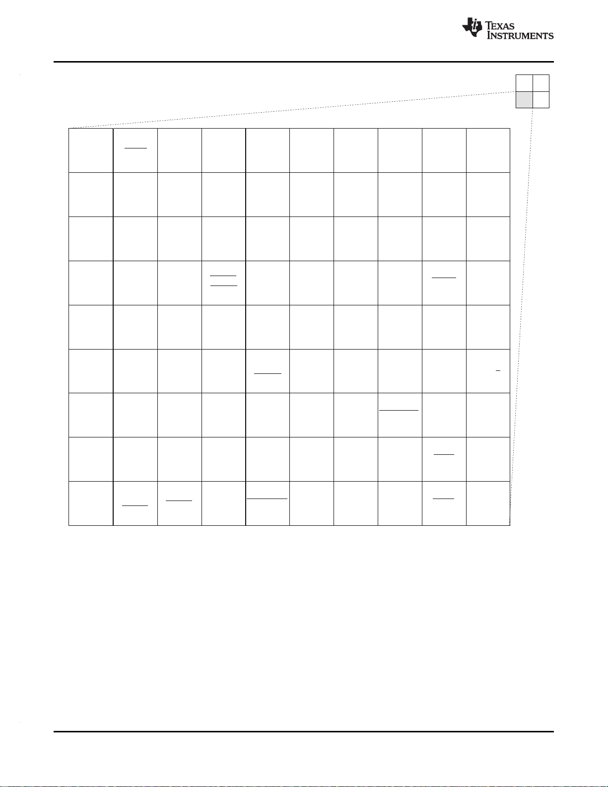
ADVANCEINFORMATION
J
H
G
F
E
D
C
B
A
10987654321
10987654321
EMA_D[15]/
GP3[7]
AXR15/
EPWM0TZ[0]/
ECAP2_APWM2/
GP0[7]
ACLKR/
PRU0_R30[20]/
GP0[15]/
PRU0_R31[22]
ACLKX/
PRU0_R30[19]/
GP0[14]/
PRU0_R31[21]
AHCLKX/
USB_REFCLKIN/
/
GP0[10]/
PRU0_R31[17]
UART1_CTS
AFSX/
GP0[12]/
PRU0_R31[19]
AFSR/
GP0[13]/
PRU0_R31[20]
AXR9/
DX1/
GP0[1]
AXR4/
FSR0/
GP1[12]/
MII_COL
AXR5/
CLKX0/
GP1[13]/
MII_TXCLK
AXR7/
EPWM1TZ[0]/
PRU0_R30[17]
GP1[15]/
PRU0_R31[7]
AXR10/
DR1/
GP0[2]
AXR1/
DX0/
GP1[9]/
MII_TXD[1]
AXR3/
FSX0/
GP1[11]/
MII_TXD[3]
AXR2/
DR0/
GP1[10]/
MII_TXD[2]
MMCSD1_DAT[6]/
LCD_MCLK/
PRU1_R30[6]/
GP8[10]/
PRU1_R31[7]
RTC_ALARM/
/
GP0[8]/
UART2_CTS
DEEPSLEEP
AXR0/
ECAP0_APWM0/
GP8[7]/
MII_TXD[0]/
CLKS0
PRU0_R30[24]/
MMCSD1_CLK/
UPP_CHB_START/
GP8[14]/
PRU1_R31[26]
MMCSD1_DAT[4]/
LCD_VSYNC/
PRU1_R30[4]/
GP8[8]/
PRU1_R31[5]
SATA_VSS
PRU0_R30[22]/
PRU1_R30[8]/
UPP_CHB_WAIT/
GP8[12]/
PRU1_R31[24]
AXR8/
CLKS1/
ECAP1_APWM1/
GP0[0]/
PRU0_R31[8]
AXR12/
FSR1/
GP0[4]
EMA_D[4]/
GP4[12]
AXR14/
CLKR1/
GP0[6]
EMA_WEN_DQM[1]/
GP2[2]
EMA_D[0]/
GP4[8]
EMA_A[19]/
MMCSD0_DAT[2]/
PRU1_R30[27]/
GP4[3]
EMA_D[9]/
GP3[1]
EMA_A_R /
GP3[9]
W
MMCSD0_CLK/
PRU1_R30[31]/
GP4[7]
EMA_D[8]/
GP3[0]
EMA_D[13]/
GP3[5]
VP_CLKIN2/
MMCSD1_DAT[3]/
PRU1_R30[3]/
GP6[4]/
PRU1_R31[4]
VP_CLKIN3/
MMCSD1_DAT[1]/
PRU1_R30[1]/
GP6[2]/
PRU1_R31[2]
AMUTE/
GP0[9]/
PRU0_R31[16]
PRU0_R30[16]/
UART2_RTS/
DV
DD3318_A
DV
DD3318_A
EMA_WE/
GP3[11]
EMA_D[10]/
GP3[2]
EMA_D[3]/
GP4[11]
EMA_SDCKE/
PRU0_R30[4]/
GP2[6]/
PRU0_R31[4]
EMA_D[14]/
GP3[6]
EMA_D[7]/
GP4[15]
EMA_D[1]/
GP4[9]
EMA_A[22]/
MMCSD0_CMD/
PRU1_R30[30]/
GP4[6]
EMA_D[2]/
GP4[10]
EMA_A[21]/
MMCSD0_DAT[0]/
PRU1_R30[29]/
GP4[5]
PRU0_R30[23]/
MMCSD1_CMD/
UPP_CHB_ENABLE/
GP8[13]/
PRU1_R31[25]
AHCLKR/
/
GP0[11]/
PRU0_R31[18]
PRU0_R30[18]/
UART1_RTS
EMA_D[12]/
GP3[4]
EMA_WEN_DQM[0]/
GP2[3]
EMA_CLK/
PRU0_R30[5]/
GP2[7]/
PRU0_R31[5]
AXR6/
CLKR0/
GP1[14]/
MII_TXEN/
PRU0_R31[6]
AXR11/
FSX1/
GP0[3]
EMA_D[6]/
GP4[14]
EMA_D[11]/
GP3[3]
RV
DD
EMA_D[5]/
GP4[13]
MMCSD1_DAT[7]/
LCD_PCLK/
PRU1_R30[7]/
GP8[11]
MMCSD1_DAT[5]/
LCD_HSYNC/
PRU1_R30[5]/
GP8[9]/
PRU1_R31[6]
PRU0_R30[25]/
MMCSD1_DAT[0]/
UPP_CHB_CLOCK/
GP8[15]/
PRU1_R31[27]
AXR13/
CLKX1/
GP0[5]
J
H
G
F
E
D
C
B
A
EMA_CS[4]/
GP3[13]
EMA_CAS/
PRU0_R30[2]/
GP2[4]/
PRU0_R31[2]
DV
DD3318_B
DV
DD3318_B
DV
DD3318_B
DV
DD3318_B
DV
DD18
CV
DD
CV
DD
DV
DD3318_B
DV
DD18
SATA_VSS
DV
DD3318_A
V
SS
V
SS
CV
DD
CV
DD
V
SS
V
SS
CV
DD
SATA_TXP
SATA_TXN
DV
DD3318_C
CV
DD
V
SS
V
SS
TMS320C6748
SPRS590B–JUNE 2009–REVISED AUGUST 2010
www.ti.com
3.7 Pin Multiplexing Control
Device level pin multiplexing is controlled by registers PINMUX0 - PINMUX19 in the SYSCFG module.
For the device family, pin multiplexing can be controlled on a pin-by-pin basis. Each pin that is multiplexed
with several different functions has a corresponding 4-bit field in one of the PINMUX registers.
Pin multiplexing selects which of several peripheral pin functions controls the pin's IO buffer output data
and output enable values only. The default pin multiplexing control for almost every pin is to select 'none'
of the peripheral functions in which case the pin's IO buffer is held tri-stated.
Note that the input from each pin is always routed to all of the peripherals that share the pin; the PINMUX
registers have no effect on input from a pin.
Figure 3-6. Pin Map (Quad D)
Submit Documentation Feedback
Product Folder Link(s): TMS320C6748
30 Device Overview Copyright © 2009–2010, Texas Instruments Incorporated
Page 31

ADVANCEINFORMATION
TMS320C6748
www.ti.com
SPRS590B–JUNE 2009–REVISED AUGUST 2010
3.8 Terminal Functions
Table 3-5 to Table 3-31 identify the external signal names, the associated pin/ball numbers along with the
mechanical package designator, the pin type (I, O, IO, OZ, or PWR), whether the pin/ball has any internal
pullup/pulldown resistors, whether the pin/ball is configurable as an IO in GPIO mode, and a functional pin
description.
3.8.1 Device Reset, NMI and JTAG
Table 3-5. Reset, NMI and JTAG Terminal Functions
SIGNAL
NAME NO.
RESET K14 I IPU B Device reset input
NMI J17 I IPU B Non-Maskable Interrupt
RESETOUT / UHPI_HAS / PRU1_R30[14] /
GP6[15]
TMS L16 I IPU B JTAG test mode select
TDI M16 I IPU B JTAG test data input
TDO J18 O IPU B JTAG test data output
TCK J15 I IPU B JTAG test clock
TRST L17 I IPD B JTAG test reset
EMU0 J16 I/O IPU B Emulation pin
EMU1 K16 I/O IPU B Emulation pin
(1) I = Input, O = Output, I/O = Bidirectional, Z = High impedance, PWR = Supply voltage, GND = Ground, A = Analog signal.
Note: For multiplexed pins where functions have different types (ie., input versus output), the table reflects the pin function direction for
that particular peripheral.
(2) IPD = Internal Pulldown resistor, IPU = Internal Pullup resistor. CP[n] = configurable pull-up/pull-down (where n is the pin group) using
the PUPDENA and PUPDSEL registers in the System Module.
(3) This signal is part of a dual-voltage IO group (A, B or C). These groups can be operated at 3.3V or 1.8V nominal. The three groups can
be operated at independent voltages but all pins withina group will operate at the same voltage. Group A operates at the voltage of
power supply DVDD3318_A. Group B operates at the voltage of power supply DVDD3318_B. Group C operates at the voltage of power
supply DVDD3318_C.
(4) Open drain mode for RESETOUT function.
T17 O
TYPE
(1)
PULL
RESET
(4)
CP[21] C Reset output
JTAG
(2)
POWER
GROUP
(3)
DESCRIPTION
Copyright © 2009–2010, Texas Instruments Incorporated Device Overview 31
Submit Documentation Feedback
Product Folder Link(s): TMS320C6748
Page 32

ADVANCEINFORMATION
TMS320C6748
SPRS590B–JUNE 2009–REVISED AUGUST 2010
www.ti.com
3.8.2 High-Frequency Oscillator and PLL
Table 3-6. High-Frequency Oscillator and PLL Terminal Functions
SIGNAL
NAME NO.
CLKOUT / UHPI_HDS2 /
PRU1_R30[13] / GP6[14]
OSCIN L19 I — — Oscillator input
OSCOUT K19 O — — Oscillator output
OSCVSS L18 GND — — Oscillator ground
PLL0_VDDA L15 PWR — — PLL analog VDD(1.2-V filtered supply)
PLL0_VSSA M17 GND — — PLL analog VSS(for filter)
PLL1_VDDA N15 PWR — — PLL analog VDD(1.2-V filtered supply)
PLL1_VSSA M15 GND — — PLL analog VSS(for filter)
(1) I = Input, O = Output, I/O = Bidirectional, Z = High impedance, PWR = Supply voltage, GND = Ground, A = Analog signal.
Note: For multiplexed pins where functions have different types (ie., input versus output), the table reflects the pin function direction for
that particular peripheral.
(2) IPD = Internal Pulldown resistor; IPU = Internal Pullup resistor; CP[n] = configurable pull-up/pull-down (where n is the pin group) using
the PUPDENA and PUPDSEL registers in the System Module.
(3) This signal is part of a dual-voltage IO group (A, B or C). These groups can be operated at 3.3V or 1.8V nominal. The three groups can
be operated at independent voltages but all pins withina group will operate at the same voltage. Group A operates at the voltage of
power supply DVDD3318_A. Group B operates at the voltage of power supply DVDD3318_B. Group C operates at the voltage of power
supply DVDD3318_C.
T18 O CP[22] C PLL Observation Clock
TYPE
(1)
PULL
1.2-V OSCILLATOR
1.2-V PLL0
1.2-V PLL1
POWER
(2)
GROUP
(3)
DESCRIPTION
32 Device Overview Copyright © 2009–2010, Texas Instruments Incorporated
Submit Documentation Feedback
Product Folder Link(s): TMS320C6748
Page 33

ADVANCEINFORMATION
TMS320C6748
www.ti.com
SPRS590B–JUNE 2009–REVISED AUGUST 2010
3.8.3 Real-Time Clock and 32-kHz Oscillator
Table 3-7. Real-Time Clock (RTC) and 1.2-V, 32-kHz Oscillator Terminal Functions
SIGNAL
NAME NO.
RTC_XI J19 I — — RTC 32-kHz oscillator input
RTC_XO H19 O — — RTC 32-kHz oscillator output
RTC_ALARM / UART2_CTS / GP0[8] / DEEPSLEEP F4 O CP[0] A RTC Alarm
RTC_CVDD L14 PWR — —
RTC_V
ss
(1) I = Input, O = Output, I/O = Bidirectional, Z = High impedance, PWR = Supply voltage, GND = Ground, A = Analog signal.
Note: For multiplexed pins where functions have different types (ie., input versus output), the table reflects the pin function direction for
that particular peripheral.
(2) IPD = Internal Pulldown resistor; IPU = Internal Pullup resistor; CP[n] = configurable pull-up/pull-down (where n is the pin group) using
the PUPDENA and PUPDSEL registers in the System Module. The pull-up and pull-down control of these pins is not active until the
device is out of reset. During reset, all of the pins associated with these registers are weakly pulled down. If the application requires a
pull-up, an external pull-up can be used.
(3) This signal is part of a dual-voltage IO group (A, B or C). These groups can be operated at 3.3V or 1.8V nominal. The three groups can
be operated at independent voltages but all pins withina group will operate at the same voltage. Group A operates at the voltage of
power supply DVDD3318_A. Group B operates at the voltage of power supply DVDD3318_B. Group C operates at the voltage of power
supply DVDD3318_C.
H18 GND — — Oscillator ground
TYPE
(1)
PULL
(2)
POWER
GROUP
(3)
RTC module core power
(isolated from chip CVDD)
DESCRIPTION
3.8.4 DEEPSLEEP Power Control
Table 3-8. DEEPSLEEP Power Control Terminal Functions
SIGNAL
NAME NO.
RTC_ALARM / UART2_CTS / GP0[8] / DEEPSLEEP F4 I CP[0] A DEEPSLEEP power control output
(1) I = Input, O = Output, I/O = Bidirectional, Z = High impedance, PWR = Supply voltage, GND = Ground, A = Analog signal.
Note: For multiplexed pins where functions have different types (ie., input versus output), the table reflects the pin function direction for
that particular peripheral.
(2) IPD = Internal Pulldown resistor; IPU = Internal Pullup resistor; CP[n] = configurable pull-up/pull-down (where n is the pin group) using
the PUPDENA and PUPDSEL registers in the System Module. The pull-up and pull-down control of these pins is not active until the
device is out of reset. During reset, all of the pins associated with these registers are weakly pulled down. If the application requires a
pull-up, an external pull-up can be used.
(3) This signal is part of a dual-voltage IO group (A, B or C). These groups can be operated at 3.3V or 1.8V nominal. The three groups can
be operated at independent voltages but all pins withina group will operate at the same voltage. Group A operates at the voltage of
power supply DVDD3318_A. Group B operates at the voltage of power supply DVDD3318_B. Group C operates at the voltage of power
supply DVDD3318_C.
TYPE
(1)
PULL
(2)
POWER
GROUP
(3)
DESCRIPTION
Copyright © 2009–2010, Texas Instruments Incorporated Device Overview 33
Submit Documentation Feedback
Product Folder Link(s): TMS320C6748
Page 34

ADVANCEINFORMATION
TMS320C6748
SPRS590B–JUNE 2009–REVISED AUGUST 2010
3.8.5 External Memory Interface A (EMIFA)
Table 3-9. External Memory Interface A (EMIFA) Terminal Functions
SIGNAL
NAME NO.
EMA_D[15] / GP3[7] E6 I/O CP[17] B
EMA_D[14] / GP3[6] C7 I/O CP[17] B
EMA_D[13] / GP3[5] B6 I/O CP[17] B
EMA_D[12] / GP3[4] A6 I/O CP[17] B
EMA_D[11] / GP3[3] D6 I/O CP[17] B
EMA_D[10] / GP3[2] A7 I/O CP[17] B
EMA_D[9] / GP3[1] D9 I/O CP[17] B
EMA_D[8] / GP3[0] E10 I/O CP[17] B
EMA_D[7] / GP4[15] D7 I/O CP[17] B
EMA_D[6] / GP4[14] C6 I/O CP[17] B
EMA_D[5] / GP4[13] E7 I/O CP[17] B
EMA_D[4] / GP4[12] B5 I/O CP[17] B
EMA_D[3] / GP4[11] E8 I/O CP[17] B
EMA_D[2] / GP4[10] B8 I/O CP[17] B
EMA_D[1] / GP4[9] A8 I/O CP[17] B
EMA_D[0] / GP4[8] C9 I/O CP[17] B
TYPE
(1)
PULL
(2)
POWER
GROUP
(3)
EMIFA data bus
www.ti.com
DESCRIPTION
(1) I = Input, O = Output, I/O = Bidirectional, Z = High impedance, PWR = Supply voltage, GND = Ground, A = Analog signal.
Note: The pin type shown refers to the input, output or high-impedance state of the pin function when configured as the signal name
highlighted in bold. All multiplexed signals may enter a high-impedance state when the configured function is input-only or the configured
function supports high-Z operation. All GPIO signals can be used as input or output. For multiplexed pins where functions have different
types (ie., input versus output), the table reflects the pin function direction for that particular peripheral.
(2) IPD = Internal Pulldown resistor; IPU = Internal Pullup resistor; CP[n] = configurable pull-up/pull-down (where n is the pin group) using
the PUPDENA and PUPDSEL registers in the System Module. The pull-up and pull-down control of these pins is not active until the
device is out of reset. During reset, all of the pins associated with these registers are weakly pulled down. If the application requires a
pull-up, an external pull-up can be used.
(3) This signal is part of a dual-voltage IO group (A, B or C). These groups can be operated at 3.3V or 1.8V nominal. The three groups can
be operated at independent voltages but all pins withina group will operate at the same voltage. Group A operates at the voltage of
power supply DVDD3318_A. Group B operates at the voltage of power supply DVDD3318_B. Group C operates at the voltage of power
supply DVDD3318_C.
34 Device Overview Copyright © 2009–2010, Texas Instruments Incorporated
Submit Documentation Feedback
Product Folder Link(s): TMS320C6748
Page 35

ADVANCEINFORMATION
TMS320C6748
www.ti.com
SPRS590B–JUNE 2009–REVISED AUGUST 2010
Table 3-9. External Memory Interface A (EMIFA) Terminal Functions (continued)
SIGNAL
NAME NO.
EMA_A[22] / MMCSD0_CMD /
PRU1_R30[30] / GP4[6]
EMA_A[21] / MMCSD0_DAT[0] /
PRU1_R30[29] / GP4[5]
EMA_A[20] / MMCSD0_DAT[1] /
PRU1_R30[28] / GP4[4]
EMA_A[19] / MMCSD0_DAT[2] /
PRU1_R30[27] / GP4[3]
EMA_A[18] / MMCSD0_DAT[3] /
PRU1_R30[26] / GP4[2]
EMA_A[17] / MMCSD0_DAT[4] /
PRU1_R30[25] / GP4[1]
EMA_A[16] / MMCSD0_DAT[5] /
PRU1_R30[24] / GP4[0]
EMA_A[15] / MMCSD0_DAT[6] /
PRU1_R30[23] / GP5[15]
EMA_A[14] / MMCSD0_DAT[7] /
PRU1_R30[22] / GP5[14] / PRU1_R31[22]
EMA_A[13] /PRU0_R30[21] / PRU1_R30[21]
/ GP5[13] / PRU1_R31[21]
EMA_A[12] / PRU1_R30[20] / GP5[12] /
PRU1_R31[20]
EMA_A[11] / PRU1_R30[19] / GP5[11] /
PRU1_R31[19]
EMA_A[10] / PRU1_R30[18] / GP5[10] /
PRU1_R31[18]
EMA_A[9] / PRU1_R30[17] / GP5[9] D12 O CP[19] B
EMA_A[8] / PRU1_R30[16] / GP5[8] A13 O CP[19] B
EMA_A[7] / PRU1_R30[15] / GP5[7] B13 O CP[20] B
EMA_A[6] / GP5[6] E13 O CP[20] B
EMA_A[5] / GP5[5] C13 O CP[20] B
EMA_A[4] / GP5[4] A14 O CP[20] B
EMA_A[3] / GP5[3] D14 O CP[20] B
EMA_A[2] / GP5[2] B14 O CP[20] B
EMA_A[1] / GP5[1] D15 O CP[20] B
EMA_A[0] / GP5[0] C14 O CP[20] B
EMA_BA[0] / GP2[8] C15 O CP[16] B
EMA_BA[1] / GP2[9] A15 O CP[16] B
EMA_CLK / PRU0_R30[5] / GP2[7] /
PRU0_R31[5]
EMA_SDCKE / PRU0_R30[4] / GP2[6] /
PRU0_R31[4]
EMA_RAS / PRU0_R30[3] / GP2[5] /
PRU0_R31[3]
EMA_CAS / PRU0_R30[2] / GP2[4] /
PRU0_R31[2]
EMA_CS[0] / GP2[0] A18 O CP[16] B EMIFA SDRAM Chip Select
EMA_CS[2] / GP3[15] B17 O CP[16] B
EMA_CS[3] / GP3[14] A17 O CP[16] B
EMA_CS[4] / GP3[13] F9 O CP[16] B
EMA_CS[5] / GP3[12] B16 O CP[16] B
EMA_A_RW / GP3[9] D10 O CP[16] B EMIFA Async Read/Write control
A10 O CP[18] B
B10 O CP[18] B
A11 O CP[18] B
C10 O CP[18] B
E11 O CP[18] B
B11 O CP[18] B
E12 O CP[18] B
C11 O CP[19] B
A12 O CP[19] B
D11 O CP[19] B
D13 O CP[19] B
B12 O CP[19] B
C12 O CP[19] B
B7 O CP[16] B EMIFA clock
D8 O CP[16] B EMIFA SDRAM clock enable
A16 O CP[16] B EMIFA SDRAM row address strobe
A9 O CP[16] B EMIFA SDRAM column address strobe
TYPE
(1)
PULL
(2)
POWER
GROUP
(3)
EMIFA address bus
EMIFA bank address
EMIFA Async chip select
DESCRIPTION
Copyright © 2009–2010, Texas Instruments Incorporated Device Overview 35
Submit Documentation Feedback
Product Folder Link(s): TMS320C6748
Page 36

ADVANCEINFORMATION
TMS320C6748
SPRS590B–JUNE 2009–REVISED AUGUST 2010
www.ti.com
Table 3-9. External Memory Interface A (EMIFA) Terminal Functions (continued)
SIGNAL
NAME NO.
EMA_WE / GP3[11] B9 O CP[16] B EMIFA SDRAM write enable
EMA_WEN_DQM[1] / GP2[2] A5 O CP[16] B
EMA_WEN_DQM[0] / GP2[3] C8 O CP[16] B EMIFA write enable/data mask for EMA_D[7:0]
EMA_OE / GP3[10] B15 O CP[16] B EMIFA output enable
EMA_WAIT[0] / PRU0_R30[0] / GP3[8] /
PRU0_R31[0]
EMA_WAIT[1] / PRU0_R30[1] / GP2[1] /
PRU0_R31[1]
B18 I CP[16] B
B19 I CP[16] B
TYPE
(1)
PULL
(2)
POWER
GROUP
(3)
EMIFA write enable/data mask for
EMA_D[15:8]
EMIFA wait input/interrupt
DESCRIPTION
36 Device Overview Copyright © 2009–2010, Texas Instruments Incorporated
Submit Documentation Feedback
Product Folder Link(s): TMS320C6748
Page 37

ADVANCEINFORMATION
TMS320C6748
www.ti.com
SPRS590B–JUNE 2009–REVISED AUGUST 2010
3.8.6 DDR2 Controller (DDR2)
Table 3-10. DDR2 Controller (DDR2) Terminal Functions
SIGNAL
NAME NO.
DDR_D[15] W10 I/O IPD
DDR_D[14] U11 I/O IPD
DDR_D[13] V10 I/O IPD
DDR_D[12] U10 I/O IPD
DDR_D[11] T12 I/O IPD
DDR_D[10] T10 I/O IPD
DDR_D[9] T11 I/O IPD
DDR_D[8] T13 I/O IPD
DDR_D[7] W11 I/O IPD
DDR_D[6] W12 I/O IPD
DDR_D[5] V12 I/O IPD
DDR_D[4] V13 I/O IPD
DDR_D[3] U13 I/O IPD
DDR_D[2] V14 I/O IPD
DDR_D[1] U14 I/O IPD
DDR_D[0] U15 I/O IPD
DDR_A[13] T5 O IPD
DDR_A[12] V4 O IPD
DDR_A[11] T4 O IPD
DDR_A[10] W4 O IPD
DDR_A[9] T6 O IPD
DDR_A[8] U4 O IPD
DDR_A[7] U6 O IPD
DDR_A[6] W5 O IPD
DDR_A[5] V5 O IPD
DDR_A[4] U5 O IPD
DDR_A[3] V6 O IPD
DDR_A[2] W6 O IPD
DDR_A[1] T7 O IPD
DDR_A[0] U7 O IPD
DDR_CLKP W8 O IPD DDR2 clock (positive)
DDR_CLKN W7 O IPD DDR2 clock (negative)
DDR_CKE V7 O IPD DDR2 clock enable
DDR_WE T8 O IPD DDR2 write enable
DDR_RAS W9 O IPD DDR2 row address strobe
DDR_CAS U9 O IPD DDR2 column address strobe
DDR_CS V9 O IPD DDR2 chip select
DDR_DQM[0] W13 O IPD
DDR_DQM[1] R10 O IPD
TYPE
(1)
PULL
(2)
DDR2 SDRAM data bus
DDR2 row/column address
DDR2 data mask outputs
DESCRIPTION
(1) I = Input, O = Output, I/O = Bidirectional, Z = High impedance, PWR = Supply voltage, GND = Ground, A = Analog signal.
Note: The pin type shown refers to the input, output or high-impedance state of the pin function when configured as the signal name
highlighted in bold. All multiplexed signals may enter a high-impedance state when the configured function is input-only or the configured
function supports high-Z operation. All GPIO signals can be used as input or output. For multiplexed pins where functions have different
types (ie., input versus output), the table reflects the pin function direction for that particular peripheral.
(2) IPD = Internal Pulldown resistor; IPU = Internal Pullup resistor; CP[n] = configurable pull-up/pull-down (where n is the pin group) using
the PUPDENA and PUPDSEL registers in the System Module.
Copyright © 2009–2010, Texas Instruments Incorporated Device Overview 37
Submit Documentation Feedback
Product Folder Link(s): TMS320C6748
Page 38

ADVANCEINFORMATION
TMS320C6748
SPRS590B–JUNE 2009–REVISED AUGUST 2010
www.ti.com
Table 3-10. DDR2 Controller (DDR2) Terminal Functions (continued)
SIGNAL
NAME NO.
DDR_DQS[0] T14 I/O IPD
DDR_DQS[1] V11 I/O IPD
DDR_BA[2] U8 O IPD
DDR_BA[1] T9 O IPD DDR2 SDRAM bank address
DDR_BA[0] V8 O IPD
DDR_DQGATE0 R11 O IPD Route to DDR and back to DDR_DQGATE1 with
DDR_DQGATE1 R12 I IPD Route to DDR and back to DDR_DQGATE0 with
DDR_ZP U12 O — of N and P channel outputs. Tie to ground via 50
DDR_VREF R6 I — Note even in the case of mDDR an external resistor
N10, P10, N9,
DDR_DVDD18 PWR — DDR PHY 1.8V power supply pins
P9, R9, P8,
R8, P7, R7,
N6
TYPE
(1)
PULL
(2)
DDR2 data strobe inputs/outputs
DDR2 loopback signal for external DQS gating.
same constraints as used for DDR clock and data.
DDR2 loopback signal for external DQS gating.
same constraints as used for DDR clock and data.
DDR2 reference output for drive strength calibration
ohm resistor @ 5% tolerance.
DDR voltage input for the DDR2/mDDR I/O buffers.
divider connected to this pin is necessary.
DESCRIPTION
38 Device Overview Copyright © 2009–2010, Texas Instruments Incorporated
Submit Documentation Feedback
Product Folder Link(s): TMS320C6748
Page 39

ADVANCEINFORMATION
TMS320C6748
www.ti.com
SPRS590B–JUNE 2009–REVISED AUGUST 2010
3.8.7 Serial Peripheral Interface Modules (SPI)
Table 3-11. Serial Peripheral Interface (SPI) Terminal Functions
SIGNAL
NAME NO.
SPI0
SPI0_CLK / EPWM0A / GP1[8] / MII_RXCLK D19 I/O CP[7] A SPI0 clock
SPI0_ENA / EPWM0B / PRU0_R30[6] / MII_RXDV C17 I/O CP[7] A SPI0 enable
SPI0_SCS[0] / TM64P1_OUT12 / GP1[6] / MDIO_D / TM64P1_IN12 D17 I/O CP[10] A
SPI0_SCS[1] / TM64P0_OUT12 / GP1[7] / MDIO_CLK /
TM64P0_IN12
SPI0_SCS[2] / UART0_RTS / GP8[1] / MII_RXD[0] /SATA_CP_DET D16 I/O CP[9] A
SPI0_SCS[3] / UART0_CTS / GP8[2] / MII_RXD[1] /
SATA_MP_SWITCH
SPI0_SCS[4] / UART0_TXD / GP8[3] / MII_RXD[2] D18 I/O CP[8] A
SPI0_SCS[5] / UART0_RXD / GP8[4] / MII_RXD[3] C19 I/O CP[8] A
SPI0_SIMO / EPWMSYNCO / GP8[5] / MII_CRS C18 I/O/Z CP[7] A
SPI0_SOMI / EPWMSYNCI / GP8[6] / MII_RXER C16 I/O/Z CP[7] A
SPI1_CLK / GP2[13] G19 I/O CP[15] A SPI1 clock
SPI1_ENA / GP2[12] H16 I/O CP[15] A SPI1 enable
SPI1_SCS[0] / EPWM1B / PRU0_R30[8] / GP2[14] / TM64P3_IN12 E19 I/O CP[14] A
SPI1_SCS[1] / EPWM1A / PRU0_R30[7] / GP2[15] / TM64P2_IN12 F18 I/O CP[14] A
SPI1_SCS[2] / UART1_TXD / SATA_CP_POD /GP1[0] F19 I/O CP[13] A
SPI1_SCS[3] / UART1_RXD / SATA_LED /GP1[1] E18 I/O CP[13] A
SPI1_SCS[4] / UART2_TXD / I2C1_SDA /GP1[2] F16 I/O CP[12] A
SPI1_SCS[5] / UART2_RXD / I2C1_SCL /GP1[3] F17 I/O CP[12] A
SPI1_SCS[6] / I2C0_SDA / TM64P3_OUT12 / GP1[4] G18 I/O CP[11] A
SPI1_SCS[7] / I2C0_SCL / TM64P2_OUT12 / GP1[5] G16 I/O CP[11] A
SPI1_SIMO / GP2[10] G17 I/O/Z CP[15] A
SPI1_SOMI / GP2[11] H17 I/O/Z CP[15] A
(1) I = Input, O = Output, I/O = Bidirectional, Z = High impedance, PWR = Supply voltage, GND = Ground, A = Analog signal.
Note: The pin type shown refers to the input, output or high-impedance state of the pin function when configured as the signal name
highlighted in bold. All multiplexed signals may enter a high-impedance state when the configured function is input-only or the configured
function supports high-Z operation. All GPIO signals can be used as input or output. For multiplexed pins where functions have different
types (ie., input versus output), the table reflects the pin function direction for that particular peripheral.
(2) IPD = Internal Pulldown resistor; IPU = Internal Pullup resistor; CP[n] = configurable pull-up/pull-down (where n is the pin group) using
the PUPDENA and PUPDSEL registers in the System Module. The pull-up and pull-down control of these pins is not active until the
device is out of reset. During reset, all of the pins associated with these registers are weakly pulled down. If the application requires a
pull-up, an external pull-up can be used.
(3) This signal is part of a dual-voltage IO group (A, B or C). These groups can be operated at 3.3V or 1.8V nominal. The three groups can
be operated at independent voltages but all pins withina group will operate at the same voltage. Group A operates at the voltage of
power supply DVDD3318_A. Group B operates at the voltage of power supply DVDD3318_B. Group C operates at the voltage of power
supply DVDD3318_C.
E16 I/O CP[10] A
E17 I/O CP[9] A
SPI1
TYPE
(1)
PULL
(2)
POWER
GROUP
(3)
DESCRIPTION
SPI0 chip selects
SPI0 data
slave-in-master-out
SPI0 data
slave-out-master-in
SPI1 chip selects
SPI1 data
slave-in-master-out
SPI1 data
slave-out-master-in
Copyright © 2009–2010, Texas Instruments Incorporated Device Overview 39
Submit Documentation Feedback
Product Folder Link(s): TMS320C6748
Page 40

ADVANCEINFORMATION
TMS320C6748
SPRS590B–JUNE 2009–REVISED AUGUST 2010
www.ti.com
3.8.8 Programmable Real-Time Unit (PRU)
Table 3-12. Programmable Real-Time Unit (PRU) Terminal Functions
SIGNAL
NAME NO.
PRU0 Output Signals
PRU0_R30[31] / UHPI_HRDY / PRU1_R30[12] / GP6[13] R17 O CP[23] C
PRU0_R30[30] / UHPI_HINT / PRU1_R30[11] / GP6[12] R16 O CP[23] C
PRU0_R30[29] / UHPI_HCNTL0 / UPP_CHA_CLOCK / GP6[11] U17 O CP[24] C
PRU0_R30[28] / UHPI_HCNTL1 / UPP_CHA_START / GP6[10] W15 O CP[24] C
PRU0_R30[27] / UHPI_HHWIL / UPP_CHA_ENABLE / GP6[9] U16 O CP[24] C
PRU0_R30[26] / UHPI_HRW / UPP_CHA_WAIT / GP6[8] /
PRU1_R31[17]
PRU0_R30[25] / MMCSD1_DAT[0] / UPP_CHB_CLOCK / GP8[15] /
PRU1_R31[27]
PRU0_R30[24] / MMCSD1_CLK / UPP_CHB_START / GP8[14] /
PRU1_R31[26] PRU0 Output Signals
PRU0_R30[23] / MMCSD1_CMD / UPP_CHB_ENABLE / GP8[13] /
PRU1_R31[25]
PRU0_R30[22] / PRU1_R30[8] / UPP_CHB_WAIT / GP8[12] /
PRU1_R31[24]
EMA_A[13] / PRU0_R30[21] / PRU1_R30[21] / GP5[13] /
PRU1_R31[21]
ACLKR / PRU0_R30[20] / GP0[15] / PRU0_R31[22] A1 O CP[0] A
ACLKX / PRU0_R30[19] / GP0[14] / PRU0_R31[21] B1 O CP[0] A
AHCLKR / PRU0_R30[18] / UART1_RTS / GP0[11] / PRU0_R31[18] A2 O CP[0] A
AXR7 / EPWM1TZ[0] / PRU0_R30[17] / GP1[15] / PRU0_R31[7] D2 O CP[4] A
T15 O CP[24] C
G1 O CP30] C
G2 O CP[30] C
J4 O CP[30] C
G3 O CP[30] C
D11 O CP[19] B
TYPE
(1)
PULL
(2)
POWER
GROUP
(3)
DESCRIPTION
(1) I = Input, O = Output, I/O = Bidirectional, Z = High impedance, PWR = Supply voltage, GND = Ground, A = Analog signal.
Note: The pin type shown refers to the input, output or high-impedance state of the pin function when configured as the signal name
highlighted in bold. All multiplexed signals may enter a high-impedance state when the configured function is input-only or the configured
function supports high-Z operation. All GPIO signals can be used as input or output. For multiplexed pins where functions have different
types (ie., input versus output), the table reflects the pin function direction for that particular peripheral.
(2) IPD = Internal Pulldown resistor; IPU = Internal Pullup resistor; CP[n] = configurable pull-up/pull-down (where n is the pin group) using
the PUPDENA and PUPDSEL registers in the System Module. The pull-up and pull-down control of these pins is not active until the
device is out of reset. During reset, all of the pins associated with these registers are weakly pulled down. If the application requires a
pull-up, an external pull-up can be used.
(3) This signal is part of a dual-voltage IO group (A, B or C). These groups can be operated at 3.3V or 1.8V nominal. The three groups can
be operated at independent voltages but all pins withina group will operate at the same voltage. Group A operates at the voltage of
power supply DVDD3318_A. Group B operates at the voltage of power supply DVDD3318_B. Group C operates at the voltage of power
supply DVDD3318_C.
40 Device Overview Copyright © 2009–2010, Texas Instruments Incorporated
Submit Documentation Feedback
Product Folder Link(s): TMS320C6748
Page 41

ADVANCEINFORMATION
TMS320C6748
www.ti.com
SPRS590B–JUNE 2009–REVISED AUGUST 2010
Table 3-12. Programmable Real-Time Unit (PRU) Terminal Functions (continued)
SIGNAL
NAME NO.
AMUTE / PRU0_R30[16] / UART2_RTS / GP0[9] / PRU0_R31[16] D5 O CP[0] A
VP_DIN[15]_VSYNC / UHPI_HD[7] / UPP_D[7] / PRU0_R30[15] /
PRU0_R31[15]
VP_DIN[14]_HSYNC / UHPI_HD[6] / UPP_D[6] / PRU0_R30[14] /
PRU0_R31[14]
VP_DIN[13]_FIELD / UHPI_HD[5] / UPP_D[5] / PRU0_R30[13] /
PRU0_R31[13]
VP_DIN[12] / UHPI_HD[4] / UPP_D[4] / PRU0_R30[12] /
PRU0_R31[12]
VP_DIN[11] / UHPI_HD[3] / UPP_D[3] / PRU0_R30[11] /
PRU0_R31[11]
VP_DIN[10] / UHPI_HD[2] / UPP_D[2] / PRU0_R30[10] /
PRU0_R31[10]
VP_DIN[9] / UHPI_HD[1] / UPP_D[1] / PRU0_R30[9] / PRU0_R31[9] R15 O CP[27] C
SPI1_SCS[0] / EPWM1B / PRU0_R30[8] / GP2[14] / TM64P3_IN12 E19 O CP[14] A
SPI1_SCS[1] / EPWM1A / PRU0_R30[7] / GP2[15] / TM64P2_IN12 F18 O CP[14] A
SPI0_ENA / EPWM0B / PRU0_R30[6] / MII_RXDV C17 O CP[7] A
EMA_CLK / PRU0_R30[5] / GP2[7] / PRU0_R31[5] B7 O CP[16] B
EMA_SDCKE / PRU0_R30[4] / GP2[6] / PRU0_R31[4] D8 O CP[16] B
EMA_RAS / PRU0_R30[3] / GP2[5] / PRU0_R31[3] A16 O CP[16] B
EMA_CAS / PRU0_R30[2] / GP2[4] / PRU0_R31[2] A9 O CP[16] B
EMA_WAIT[1] / PRU0_R30[1] / GP2[1] / PRU0_R31[1] B19 O CP[16] B
EMA_WAIT[0] / PRU0_R30[0] / GP3[8] / PRU0_R31[0] B18 O CP[16] B
V18 O CP[27] C
V19 O CP[27] C
U19 O CP[27] C
T16 O CP[27] C
R18 O CP[27] C
R19 O CP[27] C
TYPE
(1)
PULL
(2)
POWER
GROUP
(3)
DESCRIPTION
PRU0 Output Signals
Copyright © 2009–2010, Texas Instruments Incorporated Device Overview 41
Submit Documentation Feedback
Product Folder Link(s): TMS320C6748
Page 42

ADVANCEINFORMATION
TMS320C6748
SPRS590B–JUNE 2009–REVISED AUGUST 2010
Table 3-12. Programmable Real-Time Unit (PRU) Terminal Functions (continued)
SIGNAL
NAME NO.
PRU0 Input Signals
VP_DIN[7] / UHPI_HD[15] / UPP_D[15] / RMII_TXD[1] /
PRU0_R31[29]
VP_DIN[6] / UHPI_HD[14] / UPP_D[14] / RMII_TXD[0] /
PRU0_R31[28]
VP_DIN[5] / UHPI_HD[13] / UPP_D[13] / RMII_TXEN /
PRU0_R31[27]
VP_DIN[4] / UHPI_HD[12] / UPP_D[12] / RMII_RXD[1] /
PRU0_R31[26]
VP_DIN[3] / UHPI_HD[11] / UPP_D[11] / RMII_RXD[0] /
PRU0_R31[25]
VP_DIN[2] / UHPI_HD[10] / UPP_D[10] / RMII_RXER /
PRU0_R31[24]
VP_DIN[1] / UHPI_HD[9] / UPP_D[9] / RMII_MHZ_50_CLK /
PRU0_R31[23]
ACLKR / PRU0_R30[20] / GP0[15] / PRU0_R31[22] A1 I CP[0] A
ACLKX / PRU0_R30[19] / GP0[14] / PRU0_R31[21] B1 I CP[0] A
AFSR / GP0[13] / PRU0_R31[20] C2 I CP[0] A
AFSX / GP0[12] / PRU0_R31[19] B2 I CP[0] A
AHCLKR / PRU0_R30[18] / UART1_RTS / GP0[11] / PRU0_R31[18] A2 I CP[0] A
AHCLKX / USB_REFCLKIN / UART1_CTS / GP0[10] /
PRU0_R31[17]
AMUTE / PRU0_R30[16] / UART2_RTS / GP0[9] / PRU0_R31[16] D5 I CP[0] A
VP_DIN[15]_VSYNC / UHPI_HD[7] / UPP_D[7] / PRU0_R30[15] /
PRU0_R31[15]
VP_DIN[14]_HSYNC / UHPI_HD[6] / UPP_D[6] / PRU0_R30[14] /
PRU0_R31[14]
VP_DIN[13]_FIELD / UHPI_HD[5] / UPP_D[5] / PRU0_R30[13] /
PRU0_R31[13]
VP_DIN[12] / UHPI_HD[4] / UPP_D[4] / PRU0_R30[12] /
PRU0_R31[12]
VP_DIN[11] / UHPI_HD[3] / UPP_D[3] / PRU0_R30[11] /
PRU0_R31[11]
VP_DIN[10] / UHPI_HD[2] / UPP_D[2] / PRU0_R30[10] /
PRU0_R31[10]
VP_DIN[9] / UHPI_HD[1] / UPP_D[1] / PRU0_R30[9] / PRU0_R31[9] R15 I CP[27] C
AXR8 / CLKS1 / ECAP1_APWM1 / GP0[0] / PRU0_R31[8] E4 I CP[3] A
AXR7 / EPWM1TZ[0] / PRU0_R30[17] / GP1[15] / PRU0_R31[7] D2 I CP[4] A
AXR6 / CLKR0 / GP1[14] / MII_TXEN / PRU0_R31[6] C1 I CP[5] A
EMA_CLK / PRU0_R30[5] / GP2[7] / PRU0_R31[5] B7 I CP[16] B
EMA_SDCKE / PRU0_R30[4] / GP2[6] / PRU0_R31[4] D8 I CP[16] B
EMA_RAS / PRU0_R30[3] / GP2[5] / PRU0_R31[3] A16 I CP[16] B
EMA_CAS / PRU0_R30[2] / GP2[4] / PRU0_R31[2] A9 I CP[16] B
EMA_WAIT[1] / PRU0_R30[1] / GP2[1] / PRU0_R31[1] B19 I CP[16] B
EMA_WAIT[0] / PRU0_R30[0] / GP3[8] / PRU0_R31[0] B18 I CP[16] B
U18 I CP[26] C
V16 I CP[26] C
R14 I CP[26] C
W16 I CP[26] C
V17 I CP[26] C
W17 I CP[26] C
W18 I CP[26] C
A3 I CP[0] A
V18 I CP[27] C
V19 I CP[27] C
U19 I CP[27] C
T16 I CP[27] C
R18 I CP[27] C
R19 I CP[27] C
TYPE
(1)
PULL
(2)
POWER
GROUP
(3)
DESCRIPTION
PRU0 Input Signals
www.ti.com
42 Device Overview Copyright © 2009–2010, Texas Instruments Incorporated
Submit Documentation Feedback
Product Folder Link(s): TMS320C6748
Page 43

ADVANCEINFORMATION
TMS320C6748
www.ti.com
SPRS590B–JUNE 2009–REVISED AUGUST 2010
Table 3-12. Programmable Real-Time Unit (PRU) Terminal Functions (continued)
SIGNAL
NAME NO.
PRU1 Output Signals
MMCSD0_CLK / PRU1_R30[31] /GP4[7] E9 O CP[18] B
EMA_A[22] / MMCSD0_CMD / PRU1_R30[30] / GP4[6] A10 O CP[18] B
EMA_A[21] / MMCSD0_DAT[0] / PRU1_R30[29] / GP4[5] B10 O CP[18] B
EMA_A[20] / MMCSD0_DAT[1] / PRU1_R30[28] / GP4[4] A11 O CP[18] B
EMA_A[19] / MMCSD0_DAT[2] / PRU1_R30[27] / GP4[3] C10 O CP[18] B
EMA_A[18] / MMCSD0_DAT[3] / PRU1_R30[26] / GP4[2] E11 O CP[18] B
EMA_A[17] / MMCSD0_DAT[4] / PRU1_R30[25] / GP4[1] B11 O CP[18] B
EMA_A[16] / MMCSD0_DAT[5] / PRU1_R30[24] / GP4[0] E12 O CP[18] B
EMA_A[15] / MMCSD0_DAT[6] / PRU1_R30[23] / GP5[15] C11 O CP[19] B
EMA_A[14] / MMCSD0_DAT[7] / PRU1_R30[22] / GP5[14] /
PRU1_R31[22]
EMA_A[13] / PRU0_R30[21] / PRU1_R30[21] / GP5[13] /
PRU1_R31[21]
EMA_A[12] / PRU1_R30[20] / GP5[12] / PRU1_R31[20] D13 O CP[19] B
EMA_A[11] / PRU1_R30[19] / GP5[11] / PRU1_R31[19] B12 O CP[19] B
EMA_A[10] / PRU1_R30[18] / GP5[10] / PRU1_R31[18] C12 O CP[19] B
EMA_A[9] / PRU1_R30[17] / GP5[9] D12 O CP[19] B
EMA_A[8] / PRU1_R30[16] / GP5[8] A13 O CP[19] B
EMA_A[7] / PRU1_R30[15] / GP5[7] B13 O CP[20] B
RESETOUT / UHPI_HAS / PRU1_R30[14] / GP6[15] T17 O CP[21] C
CLKOUT / UHPI_HDS2 / PRU1_R30[13] / GP6[14] T18 O CP[22] C
PRU0_R30[31] / UHPI_HRDY / PRU1_R30[12] / GP6[13] R17 O CP[23] C
PRU0_R30[30] / UHPI_HINT / PRU1_R30[11] / GP6[12] R16 O CP[23] C
VP_CLKIN0 / UHPI_HCS / PRU1_R30[10] / GP6[7] /
UPP_2xTXCLK
VP_CLKIN1 / UHPI_HDS1 / PRU1_R30[9] / GP6[6] / PRU1_R31[16] V15 O CP[25] C
PRU0_R30[22] / PRU1_R30[8] / UPP_CHB_WAIT / GP8[12] /
PRU1_R31[24]
MMCSD1_DAT[7] / LCD_PCLK / PRU1_R30[7] / GP8[11] F1 O CP[31] C
MMCSD1_DAT[6] / LCD_MCLK / PRU1_R30[6] / GP8[10] /
PRU1_R31[7]
MMCSD1_DAT[5] / LCD_HSYNC / PRU1_R30[5] / GP8[9] /
PRU1_R31[6]
MMCSD1_DAT[4] / LCD_VSYNC / PRU1_R30[4] / GP8[8] /
PRU1_R31[5]
VP_CLKIN2 / MMCSD1_DAT[3] / PRU1_R30[3] / GP6[4] /
PRU1_R31[4]
VP_CLKOUT2 / MMCSD1_DAT[2] / PRU1_R30[2] / GP6[3] /
PRU1_R31[3]
VP_CLKIN3 / MMCSD1_DAT[1] / PRU1_R30[1] / GP6[2] /
PRU1_R31[2]
VP_CLKOUT3 / PRU1_R30[0] / GP6[1] / PRU1_R31[1] K4 O CP[30] C
A12 O CP[19] B
D11 O CP[19] B
W14 O CP[25] C
G3 O CP[30] C
F2 O CP[31] C
H4 O CP[31] C
G4 O CP[31] C
H3 O CP[30] C
K3 O CP[30] C
J3 O CP[30] C
TYPE
(1)
PULL
(2)
POWER
GROUP
(3)
DESCRIPTION
PRU1 Output Signals
Copyright © 2009–2010, Texas Instruments Incorporated Device Overview 43
Submit Documentation Feedback
Product Folder Link(s): TMS320C6748
Page 44

ADVANCEINFORMATION
TMS320C6748
SPRS590B–JUNE 2009–REVISED AUGUST 2010
Table 3-12. Programmable Real-Time Unit (PRU) Terminal Functions (continued)
SIGNAL
NAME NO.
PRU1 Input Signals
VP_DIN[0] / UHPI_HD[8] / UPP_D[8] / RMII_CRS_DV /
PRU1_R31[29]
LCD_AC_ENB_CS / GP6[0] / PRU1_R31[28] R5 I CP[31] C
PRU0_R30[25] / MMCSD1_DAT[0] / UPP_CHB_CLOCK / GP8[15] /
PRU1_R31[27]
PRU0_R30[24] / MMCSD1_CLK / UPP_CHB_START / GP8[14] /
PRU1_R31[26]
PRU0_R30[23] / MMCSD1_CMD / UPP_CHB_ENABLE / GP8[13] /
PRU1_R31[25]
PRU0_R30[22] / PRU1_R30[8] / UPP_CHB_WAIT / GP8[12] /
PRU1_R31[24]
MMCSD0_CLK / PRU1_R30[31] /GP4[7] E9 I CP[18] B
EMA_A[22] / MMCSD0_CMD / PRU1_R30[30] / GP4[6] A10 I CP[18] B
EMA_A[21] / MMCSD0_DAT[0] / PRU1_R30[29] / GP4[5] B10 I CP[18] B
EMA_A[20] / MMCSD0_DAT[1] / PRU1_R30[28] / GP4[4] A11 I CP[18] B
EMA_A[19] / MMCSD0_DAT[2] / PRU1_R30[27] / GP4[3] C10 I CP[18] B
EMA_A[18] / MMCSD0_DAT[3] / PRU1_R30[26] / GP4[2] E11 I CP[18] B
PRU0_R30[26] / UHPI_HRW / UPP_CHA_WAIT / GP6[8] /
PRU1_R31[17]
VP_CLKIN1 / UHPI_HDS1 / PRU1_R30[9] / GP6[6] / PRU1_R31[16] V15 I CP[25] C
VP_DOUT[7] / LCD_D[7] / UPP_XD[15] / GP7[15] / PRU1_R31[15] U2 I CP[28] C
VP_DOUT[6] / LCD_D[6] / UPP_XD[14] / GP7[14] / PRU1_R31[14] U1 I CP[28] C
VP_DOUT[5] / LCD_D[5] / UPP_XD[13] / GP7[13] / PRU1_R31[13] V3 I CP[28] C
VP_DOUT[4] / LCD_D[4] / UPP_XD[12] / GP7[12] / PRU1_R31[12] V2 I CP[28] C
VP_DOUT[3] / LCD_D[3] / UPP_XD[11] / GP7[11] / PRU1_R31[11] V1 I CP[28] C
VP_DOUT[2] / LCD_D[2] / UPP_XD[10] / GP7[10] / PRU1_R31[10] W3 I CP[28] C
VP_DOUT[1] / LCD_D[1] / UPP_XD[9] / GP7[9] / PRU1_R31[9] W2 I CP[28] C
VP_DOUT[0] / LCD_D[0] / UPP_XD[8] / GP7[8] / PRU1_R31[8] W1 I CP[28] C
MMCSD1_DAT[6] / LCD_MCLK / PRU1_R30[6] / GP8[10] /
PRU1_R31[7]
MMCSD1_DAT[5] / LCD_HSYNC / PRU1_R30[5] / GP8[9] /
PRU1_R31[6]
MMCSD1_DAT[4] / LCD_VSYNC / PRU1_R30[4] / GP8[8] /
PRU1_R31[5]
VP_CLKIN2 / MMCSD1_DAT[3] / PRU1_R30[3] / GP6[4] /
PRU1_R31[4]
VP_CLKOUT2 / MMCSD1_DAT[2] / PRU1_R30[2] / GP6[3] /
PRU1_R31[3]
VP_CLKIN3 / MMCSD1_DAT[1] / PRU1_R30[1] / GP6[2] /
PRU1_R31[2]
VP_CLKOUT3 / PRU1_R30[0] / GP6[1] / PRU1_R31[1] K4 I CP[30] C
VP_DIN[8] / UHPI_HD[0] / UPP_D[0] / GP6[5] / PRU1_R31[0] P17 I CP[27] C
W19 I CP[26] C
G1 I CP[30] C
G2 I CP[30] C
J4 I CP[30] C
G3 I CP[30] C
T15 I CP[24] C
F2 I CP[31] C
H4 I CP[31] C
G4 I CP[31] C
H3 I CP[30] C
K3 I CP[30] C
J3 I CP[30] C
TYPE
(1)
PULL
(2)
POWER
GROUP
(3)
DESCRIPTION
PRU1 Input Signals
www.ti.com
44 Device Overview Copyright © 2009–2010, Texas Instruments Incorporated
Submit Documentation Feedback
Product Folder Link(s): TMS320C6748
Page 45

ADVANCEINFORMATION
TMS320C6748
www.ti.com
SPRS590B–JUNE 2009–REVISED AUGUST 2010
3.8.9 Enhanced Capture/Auxiliary PWM Modules (eCAP0)
The eCAP Module pins function as either input captures or auxiliary PWM 32-bit outputs, depending upon
how the eCAP module is programmed.
Table 3-13. Enhanced Capture Module (eCAP) Terminal Functions
SIGNAL
NAME NO.
AXR0 / ECAP0_APWM0 / GP8[7] / MII_TXD[0] / CLKS0 F3 I/O CP[6] A
AXR8 / CLKS1 / ECAP1_APWM1 / GP0[0] / PRU0_R31[8] E4 I/O CP[3] A
AXR15 / EPWM0TZ[0] / ECAP2_APWM2 / GP0[7] A4 I/O CP[1] A
(1) I = Input, O = Output, I/O = Bidirectional, Z = High impedance, PWR = Supply voltage, GND = Ground, A = Analog signal.
Note: The pin type shown refers to the input, output or high-impedance state of the pin function when configured as the signal name
highlighted in bold. All multiplexed signals may enter a high-impedance state when the configured function is input-only or the configured
function supports high-Z operation. All GPIO signals can be used as input or output. For multiplexed pins where functions have different
types (ie., input versus output), the table reflects the pin function direction for that particular peripheral.
(2) IPD = Internal Pulldown resistor; IPU = Internal Pullup resistor; CP[n] = configurable pull-up/pull-down (where n is the pin group) using
the PUPDENA and PUPDSEL registers in the System Module. The pull-up and pull-down control of these pins is not active until the
device is out of reset. During reset, all of the pins associated with these registers are weakly pulled down. If the application requires a
pull-up, an external pull-up can be used.
(3) This signal is part of a dual-voltage IO group (A, B or C). These groups can be operated at 3.3V or 1.8V nominal. The three groups can
be operated at independent voltages but all pins withina group will operate at the same voltage. Group A operates at the voltage of
power supply DVDD3318_A. Group B operates at the voltage of power supply DVDD3318_B. Group C operates at the voltage of power
supply DVDD3318_C.
TYPE
eCAP0
eCAP1
eCAP2
(1)
PULL
(2)
POWER
GROUP
(3)
enhanced capture 0 input or
auxiliary PWM 0 output
enhanced capture 1 input or
auxiliary PWM 1 output
enhanced capture 2 input or
auxiliary PWM 2 output
DESCRIPTION
Copyright © 2009–2010, Texas Instruments Incorporated Device Overview 45
Submit Documentation Feedback
Product Folder Link(s): TMS320C6748
Page 46

ADVANCEINFORMATION
TMS320C6748
SPRS590B–JUNE 2009–REVISED AUGUST 2010
www.ti.com
3.8.10 Enhanced Pulse Width Modulators (eHRPWM)
Table 3-14. Enhanced Pulse Width Modulator (eHRPWM) Terminal Functions
SIGNAL
NAME NO.
SPI0_CLK / EPWM0A / GP1[8] / MII_RXCLK D19 I/O CP[7] A
SPI0_ENA / EPWM0B / PRU0_R30[6] / MII_RXDV C17 I/O CP[7] A eHRPWM0 B output
AXR15 / EPWM0TZ[0] / ECAP2_APWM2 / GP0[7] A4 I/O CP[1] A eHRPWM0 trip zone input
SPI0_SOMI / EPWMSYNCI / GP8[6] / MII_RXER C16 I/O CP[7] A eHRPWM0 sync input
SPI0_SIMO / EPWMSYNCO / GP8[5] / MII_CRS C18 I/O CP[7] A eHRPWM0 sync output
SPI1_SCS[1] / EPWM1A / PRU0_R30[7] / GP2[15] / eHRPWM1 A output
TM64P2_IN12 (with high-resolution)
SPI1_SCS[0] / EPWM1B / PRU0_R30[8] / GP2[14] /
TM64P3_IN12
AXR7 / EPWM1TZ[0] / PRU0_R30[17] / GP1[15] /
PRU0_R31[7]
(1) I = Input, O = Output, I/O = Bidirectional, Z = High impedance, PWR = Supply voltage, GND = Ground, A = Analog signal.
Note: The pin type shown refers to the input, output or high-impedance state of the pin function when configured as the signal name
highlighted in bold. All multiplexed signals may enter a high-impedance state when the configured function is input-only or the configured
function supports high-Z operation. All GPIO signals can be used as input or output. For multiplexed pins where functions have different
types (ie., input versus output), the table reflects the pin function direction for that particular peripheral.
(2) IPD = Internal Pulldown resistor; IPU = Internal Pullup resistor; CP[n] = configurable pull-up/pull-down (where n is the pin group) using
the PUPDENA and PUPDSEL registers in the System Module. The pull-up and pull-down control of these pins is not active until the
device is out of reset. During reset, all of the pins associated with these registers are weakly pulled down. If the application requires a
pull-up, an external pull-up can be used.
(3) This signal is part of a dual-voltage IO group (A, B or C). These groups can be operated at 3.3V or 1.8V nominal. The three groups can
be operated at independent voltages but all pins withina group will operate at the same voltage. Group A operates at the voltage of
power supply DVDD3318_A. Group B operates at the voltage of power supply DVDD3318_B. Group C operates at the voltage of power
supply DVDD3318_C.
F18 I/O CP[14] A
E19 I/O CP[14] A eHRPWM1 B output
D2 I/O CP[4] A eHRPWM1 trip zone input
(1)
TYPE
eHRPWM0
eHRPWM1
PULL
(2)
POWER
GROUP
(3)
eHRPWM0 A output
(with high-resolution)
DESCRIPTION
46 Device Overview Copyright © 2009–2010, Texas Instruments Incorporated
Submit Documentation Feedback
Product Folder Link(s): TMS320C6748
Page 47

ADVANCEINFORMATION
TMS320C6748
www.ti.com
SPRS590B–JUNE 2009–REVISED AUGUST 2010
3.8.11 Boot
Table 3-15. Boot Mode Selection Terminal Functions
SIGNAL
NAME NO.
VP_DOUT[15/]/ LCD_D[15]/ UPP_XD[7] /GP7[7] / BOOT[7] P4 I CP[29] C
VP_DOUT[14] / LCD_D[14] / UPP_XD[6] /GP7[6] / BOOT[6] R3 I CP[29] C
VP_DOUT[13] / LCD_D[13] / UPP_XD[5] /GP7[5] / BOOT[5] R2 I CP[29] C
VP_DOUT[12] / LCD_D[12] / UPP_XD[4] / GP7[4] / BOOT[4] R1 I CP[29] C
VP_DOUT[11] / LCD_D[11] / UPP_XD[3] /GP7[3] / BOOT[3] T3 I CP[29] C
VP_DOUT[10] / LCD_D[10] / UPP_XD[2] /GP7[2] / BOOT[2] T2 I CP[29] C
VP_DOUT[9] / LCD_D[9] / UPP_XD[1] /GP7[1] / BOOT[1] T1 I CP[29] C
VP_DOUT[8] / LCD_D[8] / UPP_XD[0] /GP7[0] / BOOT[0] U3 I CP[29] C
(1) Boot decoding is defined in the bootloader application report.
(2) I = Input, O = Output, I/O = Bidirectional, Z = High impedance, PWR = Supply voltage, GND = Ground, A = Analog signal.
Note: The pin type shown refers to the input, output or high-impedance state of the pin function when configured as the signal name
highlighted in bold. All multiplexed signals may enter a high-impedance state when the configured function is input-only or the configured
function supports high-Z operation. All GPIO signals can be used as input or output. For multiplexed pins where functions have different
types (ie., input versus output), the table reflects the pin function direction for that particular peripheral.
(3) IPD = Internal Pulldown resistor; IPU = Internal Pullup resistor; CP[n] = configurable pull-up/pull-down (where n is the pin group) using
the PUPDENA and PUPDSEL registers in the System Module. The pull-up and pull-down control of these pins is not active until the
device is out of reset. During reset, all of the pins associated with these registers are weakly pulled down. If the application requires a
pull-up, an external pull-up can be used.
(4) This signal is part of a dual-voltage IO group (A, B or C). These groups can be operated at 3.3V or 1.8V nominal. The three groups can
be operated at independent voltages but all pins withina group will operate at the same voltage. Group A operates at the voltage of
power supply DVDD3318_A. Group B operates at the voltage of power supply DVDD3318_B. Group C operates at the voltage of power
supply DVDD3318_C.
TYPE
(2)
PULL
(3)
(1)
POWER
GROUP
(4)
DESCRIPTION
Boot Mode Selection Pins
Copyright © 2009–2010, Texas Instruments Incorporated Device Overview 47
Submit Documentation Feedback
Product Folder Link(s): TMS320C6748
Page 48

ADVANCEINFORMATION
TMS320C6748
SPRS590B–JUNE 2009–REVISED AUGUST 2010
www.ti.com
3.8.12 Universal Asynchronous Receiver/Transmitters (UART0, UART1, UART2)
Table 3-16. Universal Asynchronous Receiver/Transmitter (UART) Terminal Functions
SIGNAL
NAME NO.
UART0
SPI0_SCS[5] / UART0_RXD / GP8[4] / MII_RXD[3] C19 I CP[8] A UART0 receive data
SPI0_SCS[4] / UART0_TXD / GP8[3] / MII_RXD[2] D18 O CP[8] A UART0 transmit data
SPI0_SCS[2] / UART0_RTS / GP8[1] / MII_RXD[0] /
SATA_CP_DET
SPI0_SCS[3] / UART0_CTS / GP8[2] / MII_RXD[1] /
SATA_MP_SWITCH
SPI1_SCS[3] / UART1_RXD / SATA_LED / GP1[1] E18 I CP[13] A UART1 receive data
SPI1_SCS[2] / UART1_TXD / SATA_CP_POD / GP1[0] F19 O CP[13] A UART1 transmit data
AHCLKR / PRU0_R30[18] / UART1_RTS /GP0[11] /
PRU0_R31[18]
AHCLKX / USB_REFCLKIN / UART1_CTS / GP0[10] /
PRU0_R31[17]
SPI1_SCS[5] / UART2_RXD / I2C1_SCL /GP1[3] F17 I CP[12] A UART2 receive data
SPI1_SCS[4] / UART2_TXD / I2C1_SDA /GP1[2] F16 O CP[12] A UART2 transmit data
AMUTE / PRU0_R30[16] / UART2_RTS / GP0[9] /
PRU0_R31[16]
RTC_ALARM / UART2_CTS / GP0[8] / DEEPSLEEP F4 I CP[0] A UART2 clear-to-send input
(1) I = Input, O = Output, I/O = Bidirectional, Z = High impedance, PWR = Supply voltage, GND = Ground, A = Analog signal.
Note: The pin type shown refers to the input, output or high-impedance state of the pin function when configured as the signal name
highlighted in bold. All multiplexed signals may enter a high-impedance state when the configured function is input-only or the configured
function supports high-Z operation. All GPIO signals can be used as input or output. For multiplexed pins where functions have different
types (ie., input versus output), the table reflects the pin function direction for that particular peripheral.
(2) IPD = Internal Pulldown resistor; IPU = Internal Pullup resistor; CP[n] = configurable pull-up/pull-down (where n is the pin group) using
the PUPDENA and PUPDSEL registers in the System Module.The pull-up and pull-down control of these pins is not active until the
device is out of reset. During reset, all of the pins associated with these registers are weakly pulled down. If the application requires a
pull-up, an external pull-up can be used.
(3) This signal is part of a dual-voltage IO group (A, B or C). These groups can be operated at 3.3V or 1.8V nominal. The three groups can
be operated at independent voltages but all pins withina group will operate at the same voltage. Group A operates at the voltage of
power supply DVDD3318_A. Group B operates at the voltage of power supply DVDD3318_B. Group C operates at the voltage of power
supply DVDD3318_C.
D16 O CP[9] A UART0 ready-to-send output
E17 I CP[9] A UART0 clear-to-send input
UART1
A2 O CP[0] A UART1 ready-to-send output
A3 I CP[0] A UART1 clear-to-send input
UART2
D5 O CP[0] A UART2 ready-to-send output
TYPE
(1)
PULL
(2)
POWER
GROUP
(3)
DESCRIPTION
48 Device Overview Copyright © 2009–2010, Texas Instruments Incorporated
Submit Documentation Feedback
Product Folder Link(s): TMS320C6748
Page 49

ADVANCEINFORMATION
TMS320C6748
www.ti.com
SPRS590B–JUNE 2009–REVISED AUGUST 2010
3.8.13 Inter-Integrated Circuit Modules(I2C0, I2C1)
Table 3-17. Inter-Integrated Circuit (I2C) Terminal Functions
SIGNAL
NAME NO.
I2C0
SPI1_SCS[6] / I2C0_SDA / TM64P3_OUT12 / GP1[4] G18 I/O CP[11] A I2C0 serial data
SPI1_SCS[7] / I2C0_SCL / TM64P2_OUT12 / GP1[5] G16 I/O CP[11] A I2C0 serial clock
I2C1
SPI1_SCS[4] / UART2_TXD / I2C1_SDA / GP1[2] F16 I/O CP[12] A I2C1 serial data
SPI1_SCS[5] / UART2_RXD / I2C1_SCL / GP1[3] F17 I/O CP[12] A I2C1 serial clock
(1) I = Input, O = Output, I/O = Bidirectional, Z = High impedance, PWR = Supply voltage, GND = Ground, A = Analog signal.
Note: The pin type shown refers to the input, output or high-impedance state of the pin function when configured as the signal name
highlighted in bold. All multiplexed signals may enter a high-impedance state when the configured function is input-only or the configured
function supports high-Z operation. All GPIO signals can be used as input or output. For multiplexed pins where functions have different
types (ie., input versus output), the table reflects the pin function direction for that particular peripheral.
(2) IPD = Internal Pulldown resistor; IPU = Internal Pullup resistor; CP[n] = configurable pull-up/pull-down (where n is the pin group) using
the PUPDENA and PUPDSEL registers in the System Module.The pull-up and pull-down control of these pins is not active until the
device is out of reset. During reset, all of the pins associated with these registers are weakly pulled down. If the application requires a
pull-up, an external pull-up can be used.
(3) This signal is part of a dual-voltage IO group (A, B or C). These groups can be operated at 3.3V or 1.8V nominal. The three groups can
be operated at independent voltages but all pins withina group will operate at the same voltage. Group A operates at the voltage of
power supply DVDD3318_A. Group B operates at the voltage of power supply DVDD3318_B. Group C operates at the voltage of power
supply DVDD3318_C.
TYPE
(1)
PULL
(2)
POWER
GROUP
(3)
DESCRIPTION
Copyright © 2009–2010, Texas Instruments Incorporated Device Overview 49
Submit Documentation Feedback
Product Folder Link(s): TMS320C6748
Page 50

ADVANCEINFORMATION
TMS320C6748
SPRS590B–JUNE 2009–REVISED AUGUST 2010
www.ti.com
3.8.14 Timers
Table 3-18. Timers Terminal Functions
SIGNAL
NAME NO.
TIMER0
SPI0_SCS[1] /TM64P0_OUT12 / GP1[7] / MDIO_CLK / TM64P0_IN12 E16 I CP[10] A Timer0 lower input
SPI0_SCS[1] / TM64P0_OUT12 / GP1[7] / MDIO_CLK / TM64P0_IN12 E16 O CP[10] A
TIMER1 (Watchdog)
SPI0_SCS[0] /TM64P1_OUT12 / GP1[6] / MDIO_D / TM64P1_IN12 D17 I CP[10] A Timer1 lower input
SPI0_SCS[0] / TM64P1_OUT12 / GP1[6] / MDIO_D /TM64P1_IN12 D17 O CP[10] A
TIMER2
SPI1_SCS[1] / EPWM1A / PRU0_R30[7] / GP2[15] / TM64P2_IN12 F18 I CP[14] A Timer2 lower input
SPI1_SCS[7] / I2C0_SCL / TM64P2_OUT12 / GP1[5] G16 O CP[11] A
TIMER3
SPI1_SCS[0] / EPWM1B / PRU0_R30[8] / GP2[14] / TM64P3_IN12 E19 I CP[14] A Timer3 lower input
SPI1_SCS[6] / I2C0_SDA / TM64P3_OUT12 / GP1[4] G18 O CP[11] A
(1) I = Input, O = Output, I/O = Bidirectional, Z = High impedance, PWR = Supply voltage, GND = Ground, A = Analog signal.
Note: The pin type shown refers to the input, output or high-impedance state of the pin function when configured as the signal name
highlighted in bold. All multiplexed signals may enter a high-impedance state when the configured function is input-only or the configured
function supports high-Z operation. All GPIO signals can be used as input or output. For multiplexed pins where functions have different
types (ie., input versus output), the table reflects the pin function direction for that particular peripheral.
(2) IPD = Internal Pulldown resistor; IPU = Internal Pullup resistor; CP[n] = configurable pull-up/pull-down (where n is the pin group) using
the PUPDENA and PUPDSEL registers in the System Module. The pull-up and pull-down control of these pins is not active until the
device is out of reset. During reset, all of the pins associated with these registers are weakly pulled down. If the application requires a
pull-up, an external pull-up can be used.
(3) This signal is part of a dual-voltage IO group (A, B or C). These groups can be operated at 3.3V or 1.8V nominal. The three groups can
be operated at independent voltages but all pins withina group will operate at the same voltage. Group A operates at the voltage of
power supply DVDD3318_A. Group B operates at the voltage of power supply DVDD3318_B. Group C operates at the voltage of power
supply DVDD3318_C.
TYPE
(1)
PULL
(2)
POWER
GROUP
(3)
Timer0 lower
output
Timer1 lower
output
Timer2 lower
output
Timer3 lower
output
DESCRIPTION
50 Device Overview Copyright © 2009–2010, Texas Instruments Incorporated
Submit Documentation Feedback
Product Folder Link(s): TMS320C6748
Page 51

ADVANCEINFORMATION
TMS320C6748
www.ti.com
SPRS590B–JUNE 2009–REVISED AUGUST 2010
3.8.15 Multichannel Audio Serial Ports (McASP)
Table 3-19. Multichannel Audio Serial Ports Terminal Functions
SIGNAL
NAME NO.
McASP0
AXR15 / EPWM0TZ[0] / ECAP2_APWM2 / GP0[7] A4 I/O CP[1] A
AXR14 / CLKR1 / GP0[6] B4 I/O CP[2] A
AXR13 / CLKX1 / GP0[5] B3 I/O CP[2] A
AXR12 / FSR1 / GP0[4] C4 I/O CP[2] A
AXR11 / FSX1 / GP0[3] C5 I/O CP[2] A
AXR10 / DR1 / GP0[2] D4 I/O CP[2] A
AXR9 / DX1 / GP0[1] C3 I/O CP[2] A
AXR8 / CLKS1 / ECAP1_APWM1 / GP0[0] / PRU0_R31[8] E4 I/O CP[3] A
AXR7 / EPWM1TZ[0] / PRU0_R30[17] / GP1[15] /
PRU0_R31[7]
AXR6 / CLKR0 / GP1[14] / MII_TXEN / PRU0_R31[6] C1 I/O CP[5] A
AXR5 / CLKX0 / GP1[13] / MII_TXCLK D3 I/O CP[5] A
AXR4 / FSR0 / GP1[12] / MII_COL D1 I/O CP[5] A
AXR3 / FSX0 / GP1[11] / MII_TXD[3] E3 I/O CP[5] A
AXR2 / DR0 / GP1[10] / MII_TXD[2] E2 I/O CP[5] A
AXR1 / DX0 / GP1[9] / MII_TXD[1] E1 I/O CP[5] A
AXR0 / ECAP0_APWM0 / GP8[7] / MII_TXD[0] / CLKS0 F3 I/O CP[6] A
AHCLKX / USB_REFCLKIN / UART1_CTS / GP0[10] /
PRU0_R31[17]
ACLKX / PRU0_R30[19]/ GP0[14]/ PRU0_R31[21] B1 I/O CP[0] A McASP0 transmit bit clock
AFSX / GP0[12] / PRU0_R31[19] B2 I/O CP[0] A McASP0 transmit frame sync
AHCLKR / PRU0_R30[18] / UART1_RTS /GP0[11] /
PRU0_R31[18]
ACLKR / PRU0_R30[20] / GP0[15] / PRU0_R31[22] A1 I/O CP[0] A McASP0 receive bit clock
AFSR / GP0[13] / PRU0_R31[20] C2 I/O CP[0] A McASP0 receive frame sync
AMUTE / PRU0_R30[16] / UART2_RTS / GP0[9] /
PRU0_R31[16]
(1) I = Input, O = Output, I/O = Bidirectional, Z = High impedance, PWR = Supply voltage, GND = Ground, A = Analog signal.
Note: The pin type shown refers to the input, output or high-impedance state of the pin function when configured as the signal name
highlighted in bold. All multiplexed signals may enter a high-impedance state when the configured function is input-only or the configured
function supports high-Z operation. All GPIO signals can be used as input or output. For multiplexed pins where functions have different
types (ie., input versus output), the table reflects the pin function direction for that particular peripheral.
(2) IPD = Internal Pulldown resistor; IPU = Internal Pullup resistor; CP[n] = configurable pull-up/pull-down (where n is the pin group) using
the PUPDENA and PUPDSEL registers in the System Module. The pull-up and pull-down control of these pins is not active until the
device is out of reset. During reset, all of the pins associated with these registers are weakly pulled down. If the application requires a
pull-up, an external pull-up can be used.
(3) This signal is part of a dual-voltage IO group (A, B or C). These groups can be operated at 3.3V or 1.8V nominal. The three groups can
be operated at independent voltages but all pins withina group will operate at the same voltage. Group A operates at the voltage of
power supply DVDD3318_A. Group B operates at the voltage of power supply DVDD3318_B. Group C operates at the voltage of power
supply DVDD3318_C.
D2 I/O CP[4] A
A3 I/O CP[0] A McASP0 transmit master clock
A2 I/O CP[0] A McASP0 receive master clock
D5 I/O CP[0] A McASP0 mute output
TYPE
(1)
PULL
(2)
POWER
GROUP
(3)
McASP0 serial data
DESCRIPTION
Copyright © 2009–2010, Texas Instruments Incorporated Device Overview 51
Submit Documentation Feedback
Product Folder Link(s): TMS320C6748
Page 52

ADVANCEINFORMATION
TMS320C6748
SPRS590B–JUNE 2009–REVISED AUGUST 2010
www.ti.com
3.8.16 Multichannel Buffered Serial Ports (McBSP)
Table 3-20. Multichannel Buffered Serial Ports (McBSPs) Terminal Functions
SIGNAL
NAME NO.
AXR0 / ECAP0_APWM0 / GP8[7] / MII_TXD[0]
/ CLKS0
AXR6 / CLKR0 / GP1[14] / MII_TXEN /
PRU0_R31[6]
AXR4 / FSR0 / GP1[12] / MII_COL D1 I/O CP[5] A McBSP0 receive frame sync
AXR2 / DR0 / GP1[10] / MII_TXD[2] E2 I CP[5] A McBSP0 receive data
AXR5 / CLKX0 / GP1[13] / MII_TXCLK D3 I/O CP[5] A McBSP0 transmit clock
AXR3 / FSX0 / GP1[11] / MII_TXD[3] E3 I/O CP[5] A McBSP0 transmit frame sync
AXR1 / DX0 / GP1[9] / MII_TXD[1] E1 O CP[5] A McBSP0 transmit data
AXR8 / CLKS1 / ECAP1_APWM1 / GP0[0] /
PRU0_R31[8]
AXR14 / CLKR1 / GP0[6] B4 I/O CP[2] A McBSP1 receive clock
AXR12 / FSR1 / GP0[4] C4 I/O CP[2] A McBSP1 receive frame sync
AXR10 / DR1 / GP0[2] D4 I CP[2] A McBSP1 receive data
AXR13 / CLKX1 / GP0[5] B3 I/O CP[2] A McBSP1 transmit clock
AXR11 / FSX1 / GP0[3] C5 I/O CP[2] A McBSP1 transmit frame sync
AXR9 / DX1 / GP0[1] C3 O CP[2] A McBSP1 transmit data
(1) I = Input, O = Output, I/O = Bidirectional, Z = High impedance, PWR = Supply voltage, GND = Ground, A = Analog signal.
Note: The pin type shown refers to the input, output or high-impedance state of the pin function when configured as the signal name
highlighted in bold. All multiplexed signals may enter a high-impedance state when the configured function is input-only or the configured
function supports high-Z operation. All GPIO signals can be used as input or output. For multiplexed pins where functions have different
types (ie., input versus output), the table reflects the pin function direction for that particular peripheral.
(2) IPD = Internal Pulldown resistor; IPU = Internal Pullup resistor; CP[n] = configurable pull-up/pull-down (where n is the pin group) using
the PUPDENA and PUPDSEL registers in the System Module. The pull-up and pull-down control of these pins is not active until the
device is out of reset. During reset, all of the pins associated with these registers are weakly pulled down. If the application requires a
pull-up, an external pull-up can be used.
(3) This signal is part of a dual-voltage IO group (A, B or C). These groups can be operated at 3.3V or 1.8V nominal. The three groups can
be operated at independent voltages but all pins withina group will operate at the same voltage. Group A operates at the voltage of
power supply DVDD3318_A. Group B operates at the voltage of power supply DVDD3318_B. Group C operates at the voltage of power
supply DVDD3318_C.
F3 I CP[6] A McBSP0 sample rate generator clock input
C1 I/O CP[5] A McBSP0 receive clock
E4 I CP[3] A McBSP1 sample rate generator clock input
TYPE
(1)
McBSP0
McBSP1
PULL
(2)
POWER
GROUP
(3)
DESCRIPTION
52 Device Overview Copyright © 2009–2010, Texas Instruments Incorporated
Submit Documentation Feedback
Product Folder Link(s): TMS320C6748
Page 53

ADVANCEINFORMATION
TMS320C6748
www.ti.com
SPRS590B–JUNE 2009–REVISED AUGUST 2010
3.8.17 Universal Serial Bus Modules (USB0, USB1)
Table 3-21. Universal Serial Bus (USB) Terminal Functions
SIGNAL
NAME NO.
USB0_DM M18 A IPD — USB0 PHY data minus
USB0_DP M19 A IPD — USB0 PHY data plus
USB0_VDDA33 N18 PWR — — USB0 PHY 3.3-V supply
USB0_ID P16 A — —
USB0_VBUS N19 A — — USB0 bus voltage
USB0_DRVVBUS K18 0 IPD B USB0 controller VBUS control output.
AHCLKX / USB_REFCLKIN / UART1_CTS /
GP0[10] / PRU0_R31[17]
USB0_VDDA18 N14 PWR — — USB0 PHY 1.8-V supply input
USB0_VDDA12 N17 A — — USB0 PHY 1.2-V LDO output for bypass cap
USB_CVDD M12 PWR — —
USB1_DM P18 A — — USB1 PHY data minus
USB1_DP P19 A — — USB1 PHY data plus
AHCLKX / USB_REFCLKIN / UART1_CTS /
GP0[10] / PRU0_R31[17]
USB1_VDDA33 P15 PWR — — USB1 PHY 3.3-V supply
USB1_VDDA18 P14 PWR — — USB1 PHY 1.8-V supply
USB_CVDD M12 PWR — —
(1) I = Input, O = Output, I/O = Bidirectional, Z = High impedance, PWR = Supply voltage, GND = Ground, A = Analog signal.
Note: The pin type shown refers to the input, output or high-impedance state of the pin function when configured as the signal name
highlighted in bold. All multiplexed signals may enter a high-impedance state when the configured function is input-only or the configured
function supports high-Z operation. All GPIO signals can be used as input or output. For multiplexed pins where functions have different
types (ie., input versus output), the table reflects the pin function direction for that particular peripheral.
(2) IPD = Internal Pulldown resistor; IPU = Internal Pullup resistor; CP[n] = configurable pull-up/pull-down (where n is the pin group) using
the PUPDENA and PUPDSEL registers in the System Module. The pull-up and pull-down control of these pins is not active until the
device is out of reset. During reset, all of the pins associated with these registers are weakly pulled down. If the application requires a
pull-up, an external pull-up can be used.
(3) This signal is part of a dual-voltage IO group (A, B or C). These groups can be operated at 3.3V or 1.8V nominal. The three groups can
be operated at independent voltages but all pins withina group will operate at the same voltage. Group A operates at the voltage of
power supply DVDD3318_A. Group B operates at the voltage of power supply DVDD3318_B. Group C operates at the voltage of power
supply DVDD3318_C.
A3 I CP[0] A USB_REFCLKIN. Optional clock input
A3 I CP[0] A USB_REFCLKIN. Optional clock input
(1)
TYPE
USB0 2.0 OTG (USB0)
USB1 1.1 OHCI (USB1)
PULL
POWER
(2)
GROUP
(3)
USB0 PHY identification
(mini-A or mini-B plug)
USB0 and USB1 core logic 1.2-V supply
input
USB0 and USB1 core logic 1.2-V supply
input
DESCRIPTION
Copyright © 2009–2010, Texas Instruments Incorporated Device Overview 53
Submit Documentation Feedback
Product Folder Link(s): TMS320C6748
Page 54

ADVANCEINFORMATION
TMS320C6748
SPRS590B–JUNE 2009–REVISED AUGUST 2010
www.ti.com
3.8.18 Ethernet Media Access Controller (EMAC)
Table 3-22. Ethernet Media Access Controller (EMAC) Terminal Functions
SIGNAL
NAME NO.
AXR6 / CLKR0 / GP1[14] / MII_TXEN / PRU0_R31[6] C1 O CP[5] A EMAC MII Transmit enable output
AXR5 / CLKX0 / GP1[13] / MII_TXCLK D3 I CP[5] A EMAC MII Transmit clock input
AXR4 / FSR0 / GP1[12] / MII_COL D1 I CP[5] A EMAC MII Collision detect input
AXR3 / FSX0 / GP1[11] / MII_TXD[3] E3 O CP[5] A
AXR2 / DR0 / GP1[10] / MII_TXD[2] E2 O CP[5] A
AXR1 / DX0 / GP1[9] / MII_TXD[1] E1 O CP[5] A
AXR0 / ECAP0_APWM0 / GP8[7] / MII_TXD[0] /
CLKS0
EPWMSYNCI / GP8[6] / MII_RXER C16 I CP[7] A EMAC MII receive error input
SPI0_SIMO /EPWMSYNCO / GP8[5] / MII_CRS C18 I CP[7] A EMAC MII carrier sense input
SPI0_CLK / EPWM0A / GP1[8] / MII_RXCLK D19 I CP[7] A EMAC MII receive clock input
SPI0_ENA / EPWM0B / PRU0_R30[6] / MII_RXDV C17 I CP[7] A EMAC MII receive data valid input
SPI0_SCS[5] /UART0_RXD / GP8[4] / MII_RXD[3] C19 I CP[8] A
SPI0_SCS[4] /UART0_TXD / GP8[3] / MII_RXD[2] D18 I CP[8] A
SPI0_SCS[3] / UART0_CTS / GP8[2] / MII_RXD[1] /
SATA_MP_SWITCH
SPI0_SCS[2] / UART0_RTS / GP8[1] / MII_RXD[0] /
SATA_CP_DET
(1) I = Input, O = Output, I/O = Bidirectional, Z = High impedance, PWR = Supply voltage, GND = Ground, A = Analog signal.
Note: The pin type shown refers to the input, output or high-impedance state of the pin function when configured as the signal name
highlighted in bold. All multiplexed signals may enter a high-impedance state when the configured function is input-only or the configured
function supports high-Z operation. All GPIO signals can be used as input or output. For multiplexed pins where functions have different
types (ie., input versus output), the table reflects the pin function direction for that particular peripheral.
(2) IPD = Internal Pulldown resistor; IPU = Internal Pullup resistor; CP[n] = configurable pull-up/pull-down (where n is the pin group) using
the PUPDENA and PUPDSEL registers in the System Module. The pull-up and pull-down control of these pins is not active until the
device is out of reset. During reset, all of the pins associated with these registers are weakly pulled down. If the application requires a
pull-up, an external pull-up can be used.
(3) This signal is part of a dual-voltage IO group (A, B or C). These groups can be operated at 3.3V or 1.8V nominal. The three groups can
be operated at independent voltages but all pins withina group will operate at the same voltage. Group A operates at the voltage of
power supply DVDD3318_A. Group B operates at the voltage of power supply DVDD3318_B. Group C operates at the voltage of power
supply DVDD3318_C.
F3 O CP[6] A
E17 I CP[9] A
D16 I CP[9] A
TYPE
MII
(1)
PULL
(2)
POWER
GROUP
(3)
EMAC MII transmit data
EMAC MII receive data
DESCRIPTION
54 Device Overview Copyright © 2009–2010, Texas Instruments Incorporated
Submit Documentation Feedback
Product Folder Link(s): TMS320C6748
Page 55

ADVANCEINFORMATION
TMS320C6748
www.ti.com
Table 3-22. Ethernet Media Access Controller (EMAC) Terminal Functions (continued)
SIGNAL
NAME NO.
VP_DIN[1] / UHPI_HD[9] / UPP_D[9] /
RMII_MHZ_50_CLK / PRU0_R31[23]
VP_DIN[2] / UHPI_HD[10] / UPP_D[10] / RMII_RXER /
PRU0_R31[24]
VP_DIN[3] / UHPI_HD[11] / UPP_D[11] / RMII_RXD[0]
/ PRU0_R31[25]
VP_DIN[4] / UHPI_HD[12] / UPP_D[12] / RMII_RXD[1]
/PRU0_R31[26]
VP_DIN[0] / UHPI_HD[8] / UPP_D[8] / RMII_CRS_DV/
PRU1_R31[29]
VP_DIN[5] / UHPI_HD[13] / UPP_D[13] / RMII_TXEN
/PRU0_R31[27]
VP_DIN[6] / UHPI_HD[14] / UPP_D[14] / RMII_TXD[0]
/ PRU0_R31[28]
VP_DIN[7] / UHPI_HD[15] / UPP_D[15] / RMII_TXD[1]
/ PRU0_R31[29]
SPI0_SCS[0] /TM64P1_OUT12 / GP1[6] / MDIO_D /
TM64P1_IN12
SPI0_SCS[1] /TM64P0_OUT12 / GP1[7] / MDIO_CLK
/ TM64P0_IN12
SPRS590B–JUNE 2009–REVISED AUGUST 2010
(1)
TYPE
RMII
W18 I/O CP[26] C EMAC 50-MHz clock input or output
W17 I CP[26] C EMAC RMII receiver error
V17 I CP[26] C
W16 I CP[26] C
W19 I CP[26] C EMAC RMII carrier sense data valid
R14 O CP[26] C EMAC RMII transmit enable
V16 O CP[26] C
U18 O CP[26] C
MDIO
D17 I/O CP[10] A MDIO serial data
E16 O CP[10] A MDIO clock
PULL
(2)
POWER
GROUP
(3)
EMAC RMII receive data
EMAC RMII transmit data
DESCRIPTION
Copyright © 2009–2010, Texas Instruments Incorporated Device Overview 55
Submit Documentation Feedback
Product Folder Link(s): TMS320C6748
Page 56

ADVANCEINFORMATION
TMS320C6748
SPRS590B–JUNE 2009–REVISED AUGUST 2010
www.ti.com
3.8.19 Multimedia Card/Secure Digital (MMC/SD)
Table 3-23. Multimedia Card/Secure Digital (MMC/SD) Terminal Functions
SIGNAL
NAME NO.
MMCSD0
MMCSD0_CLK / PRU1_R30[31] /GP4[7] E9 O CP[18] B MMCSD0 Clock
EMA_A[22] / MMCSD0_CMD / PRU1_R30[30] / GP4[6] A10 I/O CP[18] B MMCSD0 Command
EMA_A[14] / MMCSD0_DAT[7] / PRU1_R30[22] / GP5[14] /
PRU1_R31[22]
EMA_A[15] / MMCSD0_DAT[6] / PRU1_R30[23] / GP5[15] C11 I/O CP[19] B
EMA_A[16] / MMCSD0_DAT[5] / PRU1_R30[24] / GP4[0] E12 I/O CP[18] B
EMA_A[17] / MMCSD0_DAT[4] / PRU1_R30[25] / GP4[1] B11 I/O CP[18] B
EMA_A[18] / MMCSD0_DAT[3] / PRU1_R30[26] / GP4[2] E11 I/O CP[18] B
EMA_A[19] / MMCSD0_DAT[2] / PRU1_R30[27] / GP4[3] C10 I/O CP[18] B
EMA_A[20] / MMCSD0_DAT[1] / PRU1_R30[28] / GP4[4] A11 I/O CP[18] B
EMA_A[21] / MMCSD0_DAT[0] / PRU1_R30[29] / GP4[5] B10 I/O CP[18] B
PRU0_R30[24] /MMCSD1_CLK / UPP_CHB_START /
GP8[14]/PRU1_R31[26]/
PRU0_R30[23] /MMCSD1_CMD / UPP_CHB_ENABLE /
GP8[13]/PRU1_R31[25]
MMCSD1_DAT[7] / LCD_PCLK / PRU1_R30[7] / GP8[11] F1 I/O CP[31] C
MMCSD1_DAT[6] / LCD_MCLK /PRU1_R30[6] / GP8[10] /
PRU1_R31[7]
MMCSD1_DAT[5] / LCD_HSYNC /PRU1_R30[5] / GP8[9] /
PRU1_R31[6]
MMCSD1_DAT[4] / LCD_VSYNC /PRU1_R30[4] / GP8[8] /
PRU1_R31[5]
VP_CLKIN2 / MMCSD1_DAT[3] / PRU1_R30[3] / GP6[4] /
PRU1_R31[4]
VP_CLKOUT2 / MMCSD1_DAT[2] / PRU1_R30[2] / GP6[3] /
PRU1_R31[3]
VP_CLKIN3 / MMCSD1_DAT[1]/ PRU1_R30[1] / GP6[2] /
PRU1_R31[2]
PRU0_R30[25] / MMCSD1_DAT[0] / UPP_CHB_CLOCK / GP8[15]/
PRU1_R31[27]
(1) I = Input, O = Output, I/O = Bidirectional, Z = High impedance, PWR = Supply voltage, GND = Ground, A = Analog signal.
Note: The pin type shown refers to the input, output or high-impedance state of the pin function when configured as the signal name
highlighted in bold. All multiplexed signals may enter a high-impedance state when the configured function is input-only or the configured
function supports high-Z operation. All GPIO signals can be used as input or output. For multiplexed pins where functions have different
types (ie., input versus output), the table reflects the pin function direction for that particular peripheral.
(2) IPD = Internal Pulldown resistor; IPU = Internal Pullup resistor; CP[n] = configurable pull-up/pull-down (where n is the pin group) using
the PUPDENA and PUPDSEL registers in the System Module. The pull-up and pull-down control of these pins is not active until the
device is out of reset. During reset, all of the pins associated with these registers are weakly pulled down. If the application requires a
pull-up, an external pull-up can be used.
(3) This signal is part of a dual-voltage IO group (A, B or C). These groups can be operated at 3.3V or 1.8V nominal. The three groups can
be operated at independent voltages but all pins withina group will operate at the same voltage. Group A operates at the voltage of
power supply DVDD3318_A. Group B operates at the voltage of power supply DVDD3318_B. Group C operates at the voltage of power
supply DVDD3318_C.
A12 I/O CP[19] B
MMCSD1
G2 O CP[30] C MMCSD1 Clock
J4 I/O CP[30] C MMCSD1 Command
F2 I/O CP[31] C
H4 I/O CP[31] C
G4 I/O CP[31] C
H3 I/O CP[30] C
K3 I/O CP[30] C
J3 I/O CP[30] C
G1 I/O CP[30] C
TYPE
(1)
PULL
(2)
POWER
GROUP
(3)
MMC/SD0 data
MMC/SD1 data
DESCRIPTION
56 Device Overview Copyright © 2009–2010, Texas Instruments Incorporated
Submit Documentation Feedback
Product Folder Link(s): TMS320C6748
Page 57

ADVANCEINFORMATION
TMS320C6748
www.ti.com
SPRS590B–JUNE 2009–REVISED AUGUST 2010
3.8.20 Liquid Crystal Display Controller(LCD)
Table 3-24. Liquid Crystal Display Controller (LCD) Terminal Functions
SIGNAL
NAME NO.
VP_DOUT[15] / LCD_D[15] / UPP_XD[7] / GP7[7] / BOOT[7] P4 I/O CP[29] C
VP_DOUT[14] / LCD_D[14] / UPP_XD[6] / GP7[6] / BOOT[6] R3 I/O CP[29] C
VP_DOUT[13] / LCD_D[13] / UPP_XD[5] / GP7[5] / BOOT[5] R2 I/O CP[29] C
VP_DOUT[12] / LCD_D[12] / UPP_XD[4] / GP7[4] / BOOT[4] R1 I/O CP[29] C
VP_DOUT[11] / LCD_D[11] / UPP_XD[3] / GP7[3] / BOOT[3] T3 I/O CP[29] C
VP_DOUT[10] / LCD_D[10] / UPP_XD[2] / GP7[2] / BOOT[2] T2 I/O CP[29] C
VP_DOUT[9] / LCD_D[9] / UPP_XD[1] / GP7[1] / BOOT[1] T1 I/O CP[29] C
VP_DOUT[8] / LCD_D[8] / UPP_XD[0] / GP7[0] / BOOT[0] U3 I/O CP[29] C
VP_DOUT[7] / LCD_D[7] / UPP_XD[15] / GP7[15] /
PRU1_R31[15]
VP_DOUT[6] / LCD_D[6] / UPP_XD[14] / GP7[14] /
PRU1_R31[14]
VP_DOUT[5] / LCD_D[5] / UPP_XD[13] / GP7[13] /
PRU1_R31[13]
VP_DOUT[4] / LCD_D[4] / UPP_XD[12] / GP7[12] /
PRU1_R31[12]
VP_DOUT[3] / LCD_D[3] / UPP_XD[11] / GP7[11] /
PRU1_R31[11]
VP_DOUT[2] / LCD_D[2] / UPP_XD[10] / GP7[10] /
PRU1_R31[10]
VP_DOUT[1] / LCD_D[1] / UPP_XD[9] / GP7[9] / PRU1_R31[9] W2 I/O CP[28] C
VP_DOUT[0] / LCD_D[0] / UPP_XD[8] / GP7[8] / PRU1_R31[8] W1 I/O CP[28] C
MMCSD1_DAT[7] / LCD_PCLK / PRU1_R30[7] / GP8[11] F1 O CP[31] C LCD pixel clock
MMCSD1_DAT[5] / LCD_HSYNC / PRU1_R30[5] / GP8[9] /
PRU1_R31[6]
MMCSD1_DAT[4] / LCD_VSYNC / PRU1_R30[4] / GP8[8] /
PRU1_R31[5]
LCD_AC_ENB_CS / GP6[0]/ / PRU1_R31[28] R5 O CP[31] C
MMCSD1_DAT[6] / LCD_MCLK / PRU1_R30[6] / GP8[10] /
PRU1_R31[7]
(1) I = Input, O = Output, I/O = Bidirectional, Z = High impedance, PWR = Supply voltage, GND = Ground, A = Analog signal.
Note: The pin type shown refers to the input, output or high-impedance state of the pin function when configured as the signal name
highlighted in bold. All multiplexed signals may enter a high-impedance state when the configured function is input-only or the configured
function supports high-Z operation. All GPIO signals can be used as input or output. For multiplexed pins where functions have different
types (ie., input versus output), the table reflects the pin function direction for that particular peripheral.
(2) IPD = Internal Pulldown resistor; IPU = Internal Pullup resistor; CP[n] = configurable pull-up/pull-down (where n is the pin group) using
the PUPDENA and PUPDSEL registers in the System Module. The pull-up and pull-down control of these pins is not active until the
device is out of reset. During reset, all of the pins associated with these registers are weakly pulled down. If the application requires a
pull-up, an external pull-up can be used.
(3) This signal is part of a dual-voltage IO group (A, B or C). These groups can be operated at 3.3V or 1.8V nominal. The three groups can
be operated at independent voltages but all pins withina group will operate at the same voltage. Group A operates at the voltage of
power supply DVDD3318_A. Group B operates at the voltage of power supply DVDD3318_B. Group C operates at the voltage of power
supply DVDD3318_C.
U2 I/O CP[28] C
U1 I/O CP[28] C
V3 I/O CP[28] C
V2 I/O CP[28] C
V1 I/O CP[28] C
W3 I/O CP[28] C
H4 O CP[31] C LCD horizontal sync
G4 O CP[31] C LCD vertical sync
F2 O CP[31] C LCD memory clock
TYPE
(1)
PULL
POWER
(2)
GROUP
(3)
DESCRIPTION
LCD data bus
LCD AC bias enable chip
select
Copyright © 2009–2010, Texas Instruments Incorporated Device Overview 57
Submit Documentation Feedback
Product Folder Link(s): TMS320C6748
Page 58

ADVANCEINFORMATION
TMS320C6748
SPRS590B–JUNE 2009–REVISED AUGUST 2010
www.ti.com
3.8.21 Serial ATA Controller (SATA)
Table 3-25. Serial ATA Controller (SATA) Terminal Functions
SIGNAL
NAME NO.
SATA_RXP L1 I — — SATA receive data (positive)
SATA_RXN L2 I — — SATA receive data (negative)
SATA_TXP J1 O — — SATA transmit data (positive)
SATA_TXN J2 O — — SATA transmit data (negative)
SATA_REFCLKP N2 I — — SATA PHY reference clock (positive)
SATA_REFCLKN N1 I — — SATA PHY reference clock (negative)
SPI0_SCS[3] / UART0_CTS / GP8[2] /
MII_RXD[1] / SATA_MP_SWITCH
SPI0_SCS[2] / UART0_RTS / GP8[1] /
MII_RXD[0] / SATA_CP_DET
SPI1_SCS[2] / UART1_TXD /
SATA_CP_POD / GP1[0]
SPI1_SCS[3] / UART1_RXD / SATA_LED /
GP1[1]
SATA_REG N3 A — —
SATA_VDDR P3 PWR — — SATA PHY 1.8V internal regulator supply
SATA_VDD PWR — — SATA PHY 1.2V logic supply
SATA_VSS GND — — SATA PHY ground reference
(1) I = Input, O = Output, I/O = Bidirectional, Z = High impedance, PWR = Supply voltage, GND = Ground, A = Analog signal.
Note: The pin type shown refers to the input, output or high-impedance state of the pin function when configured as the signal name
highlighted in bold. All multiplexed signals may enter a high-impedance state when the configured function is input-only or the configured
function supports high-Z operation. All GPIO signals can be used as input or output. For multiplexed pins where functions have different
types (ie., input versus output), the table reflects the pin function direction for that particular peripheral.
(2) IPD = Internal Pulldown resistor; IPU = Internal Pullup resistor; CP[n] = configurable pull-up/pull-down (where n is the pin group) using
the PUPDENA and PUPDSEL registers in the System Module. The pull-up and pull-down control of these pins is not active until the
device is out of reset. During reset, all of the pins associated with these registers are weakly pulled down. If the application requires a
pull-up, an external pull-up can be used.
(3) This signal is part of a dual-voltage IO group (A, B or C). These groups can be operated at 3.3V or 1.8V nominal. The three groups can
be operated at independent voltages but all pins withina group will operate at the same voltage. Group A operates at the voltage of
power supply DVDD3318_A. Group B operates at the voltage of power supply DVDD3318_B. Group C operates at the voltage of power
supply DVDD3318_C.
E17 I CP[9] A SATA mechanical presence switch input
D16 I CP[9] A SATA cold presence detect input
F19 O CP[13] A SATA cold presence power-on output
E18 O CP[13] A SATA LED control output
M2,
P1,
P2,
N4
H1,
H2,
K1,
K2,
L3,
M1
TYPE
(1)
PULL
(2)
POWER
GROUP
(3)
SATA PHY PLL regulator output. Requires an
external 0.1uF filter capacitor.
DESCRIPTION
58 Device Overview Copyright © 2009–2010, Texas Instruments Incorporated
Submit Documentation Feedback
Product Folder Link(s): TMS320C6748
Page 59

ADVANCEINFORMATION
TMS320C6748
www.ti.com
SPRS590B–JUNE 2009–REVISED AUGUST 2010
3.8.22 Universal Host-Port Interface (UHPI)
Table 3-26. Universal Host-Port Interface (UHPI) Terminal Functions
SIGNAL
NAME NO.
VP_DIN[7] / UHPI_HD[15] / UPP_D[15] / RMII_TXD[1] /
PRU0_R31[29]
VP_DIN[6] / UHPI_HD[14] / UPP_D[14] / RMII_TXD[0] /
PRU0_R31[28]
VP_DIN[5] / UHPI_HD[13] / UPP_D[13] / RMII_TXEN /
PRU0_R31[27]
VP_DIN[4] / UHPI_HD[12] / UPP_D[12] / RMII_RXD[1] /
PRU0_R31[26]
VP_DIN[3] / UHPI_HD[11] / UPP_D[11] / RMII_RXD[0] /
PRU0_R31[25]
VP_DIN[2] / UHPI_HD[10] / UPP_D[10] / RMII_RXER /
PRU0_R31[24]
VP_DIN[1] / UHPI_HD[9] / UPP_D[9] / RMII_MHZ_50_CLK /
PRU0_R31[23]
VP_DIN[0] / UHPI_HD[8] / UPP_D[8] / RMII_CRS_DV /
PRU1_R31[29]
VP_DIN[15]_VSYNC / UHPI_HD[7] / UPP_D[7]/PRU0_R30[15] /
PRU0_R31[15]
VP_DIN[14]_HSYNC / UHPI_HD[6] / UPP_D[6]/ PRU0_R30[14] /
PRU0_R31[14]
VP_DIN[13]_FIELD / UHPI_HD[5] / UPP_D[5] / PRU0_R30[13] /
PRU0_R31[13]
VP_DIN[12] / UHPI_HD[4] / UPP_D[4] / PRU0_R30[12] /
PRU0_R31[12]
VP_DIN[11] / UHPI_HD[3] / UPP_D[3] / PRU0_R30[11] /
PRU0_R31[11]
VP_DIN[10] / UHPI_HD[2] / UPP_D[2] / PRU0_R30[10] /
PRU0_R31[10]
VP_DIN[9] / UHPI_HD[1] / UPP_D[1] / PRU0_R30[9] / PRU0_R31[9] R15 I/O CP[27] C
VP_DIN[8] / UHPI_HD[0] / UPP_D[0] / GP6[5] / PRU1_R31[0] P17 I/O CP[27] C
PRU0_R30[29] / UHPI_HCNTL0 / UPP_CHA_CLOCK / GP6[11] U17 I CP[24] C
PRU0_R30[28] / UHPI_HCNTL1 / UPP_CHA_START / GP6[10] W15 I CP[24] C
PRU0_R30[27] / UHPI_HHWIL / UPP_CHA_ENABLE / GP6[9] U16 I CP[24] C
PRU0_R30[26] /UHPI_HRW / UPP_CHA_WAIT /
GP6[8]/PRU1_R31[17]
VP_CLKIN0 / UHPI_HCS / PRU1_R30[10] / GP6[7] / UPP_2xTXCLK W14 I CP[25] C UHPI chip select
VP_CLKIN1 / UHPI_HDS1 / PRU1_R30[9] / GP6[6] / PRU1_R31[16] V15 I CP[25] C
CLKOUT / UHPI_HDS2 / PRU1_R30[13] / GP6[14] T18 I CP[22] C
PRU0_R30[30] / UHPI_HINT / PRU1_R30[11] / GP6[12] R16 O CP[23] C UHPI host interrupt
U18 I/O CP[26] C
V16 I/O CP[26] C
R14 I/O CP[26] C
W16 I/O CP[26] C
V17 I/O CP[26] C
W17 I/O CP[26] C
W18 I/O CP[26] C
W19 I/O CP[26] C
V18 I/O CP[27] C
V19 I/O CP[27] C
U19 I/O CP[27] C
T16 I/O CP[27] C
R18 I/O CP[27] C
R19 I/O CP[27] C
T15 I CP[24] C UHPI read/write
TYPE
(1)
PULL
(2)
POWER
GROUP
(3)
DESCRIPTION
UHPI data bus
UHPI access control
UHPI half-word
identification control
UHPI data strobe
(1) I = Input, O = Output, I/O = Bidirectional, Z = High impedance, PWR = Supply voltage, GND = Ground, A = Analog signal.
Note: The pin type shown refers to the input, output or high-impedance state of the pin function when configured as the signal name
highlighted in bold. All multiplexed signals may enter a high-impedance state when the configured function is input-only or the configured
function supports high-Z operation. All GPIO signals can be used as input or output. For multiplexed pins where functions have different
types (ie., input versus output), the table reflects the pin function direction for that particular peripheral.
(2) IPD = Internal Pulldown resistor; IPU = Internal Pullup resistor; CP[n] = configurable pull-up/pull-down (where n is the pin group) using
the PUPDENA and PUPDSEL registers in the System Module. The pull-up and pull-down control of these pins is not active until the
device is out of reset. During reset, all of the pins associated with these registers are weakly pulled down. If the application requires a
pull-up, an external pull-up can be used.
(3) This signal is part of a dual-voltage IO group (A, B or C). These groups can be operated at 3.3V or 1.8V nominal. The three groups can
be operated at independent voltages but all pins withina group will operate at the same voltage. Group A operates at the voltage of
power supply DVDD3318_A. Group B operates at the voltage of power supply DVDD3318_B. Group C operates at the voltage of power
supply DVDD3318_C.
Copyright © 2009–2010, Texas Instruments Incorporated Device Overview 59
Submit Documentation Feedback
Product Folder Link(s): TMS320C6748
Page 60

ADVANCEINFORMATION
TMS320C6748
SPRS590B–JUNE 2009–REVISED AUGUST 2010
www.ti.com
Table 3-26. Universal Host-Port Interface (UHPI) Terminal Functions (continued)
SIGNAL
NAME NO.
PRU0_R30[31] / UHPI_HRDY / PRU1_R30[12] /GP6[13] R17 O CP[23] C UHPI ready
RESETOUT / UHPI_HAS / PRU1_R30[14] / GP6[15] T17 I CP[21] C UHPI address strobe
TYPE
(1)
PULL
(2)
POWER
GROUP
(3)
DESCRIPTION
60 Device Overview Copyright © 2009–2010, Texas Instruments Incorporated
Submit Documentation Feedback
Product Folder Link(s): TMS320C6748
Page 61

ADVANCEINFORMATION
TMS320C6748
www.ti.com
SPRS590B–JUNE 2009–REVISED AUGUST 2010
3.8.23 Universal Parallel Port (uPP)
Table 3-27. Universal Parallel Port (uPP) Terminal Functions
SIGNAL
NAME NO.
VP_CLKIN0 / UHPI_HCS1 /PRU1_R30[10] / GP6[7] / uPP 2x transmit clock
UPP_2xTXCLK input
PRU0_R30[25] /MMCSD1_DAT[0] / UPP_CHB_CLOCK /
GP8[15]/PRU1_R31[27]
PRU0_R30[24]/ MMCSD1_CLK / UPP_CHB_START / GP8[14] /
PRU1_R31[26]
PRU0_R30[23] / MMCSD1_CMD / UPP_CHB_ENABLE /
GP8[13]/PRU1_R31[25]
PRU0_R30[22] / PRU1_R30[8] / UPP_CHB_WAIT / GP8[12]/
PRU1_R31[24]
PRU0_R30[29] /UHPI_CNTL0 / UPP_CHA_CLOCK / GP6[11] U17 I/O CP[24] C uPP channel A clock
PRU0_R30[28] / UHPI_HCNTL1 / UPP_CHA_START / GP6[10] W15 I/O CP[24] C uPP channel A start
PRU0_R30[27] / UHPI_HHWIL / UPP_CHA_ENABLE / GP6[9] U16 I/O CP[24] C uPP channel A enable
PRU0_R30[26] /UHPI_HRW / UPP_CHA_WAIT / GP6[8] /
PRU1_R31[17]
W14 I CP[25] C
G1 I/O CP[30] C uPP channel B clock
G2 I/O CP[30] C uPP channel B start
J4 I/O CP[30] C uPP channel B enable
G3 I/O CP[30] C uPP channel B wait
T15 I/O CP[24] C uPP channel A wait
TYPE
(1)
PULL
POWER
(2)
GROUP
(3)
DESCRIPTION
(1) I = Input, O = Output, I/O = Bidirectional, Z = High impedance, PWR = Supply voltage, GND = Ground, A = Analog signal.
Note: The pin type shown refers to the input, output or high-impedance state of the pin function when configured as the signal name
highlighted in bold. All multiplexed signals may enter a high-impedance state when the configured function is input-only or the configured
function supports high-Z operation. All GPIO signals can be used as input or output. For multiplexed pins where functions have different
types (ie., input versus output), the table reflects the pin function direction for that particular peripheral.
(2) IPD = Internal Pulldown resistor; IPU = Internal Pullup resistor; CP[n] = configurable pull-up/pull-down (where n is the pin group) using
the PUPDENA and PUPDSEL registers in the System Module. The pull-up and pull-down control of these pins is not active until the
device is out of reset. During reset, all of the pins associated with these registers are weakly pulled down. If the application requires a
pull-up, an external pull-up can be used.
(3) This signal is part of a dual-voltage IO group (A, B or C). These groups can be operated at 3.3V or 1.8V nominal. The three groups can
be operated at independent voltages but all pins withina group will operate at the same voltage. Group A operates at the voltage of
power supply DVDD3318_A. Group B operates at the voltage of power supply DVDD3318_B. Group C operates at the voltage of power
supply DVDD3318_C.
Copyright © 2009–2010, Texas Instruments Incorporated Device Overview 61
Submit Documentation Feedback
Product Folder Link(s): TMS320C6748
Page 62

ADVANCEINFORMATION
TMS320C6748
SPRS590B–JUNE 2009–REVISED AUGUST 2010
Table 3-27. Universal Parallel Port (uPP) Terminal Functions (continued)
SIGNAL
NAME NO.
VP_DOUT[7] / LCD_D[7] / UPP_XD[15] / GP7[15] /
PRU1_R31[15]
VP_DOUT[6] / LCD_D[6] / UPP_XD[14] / GP7[14] /
PRU1_R31[14]
VP_DOUT[5] / LCD_D[5] / UPP_XD[13] / GP7[13] /
PRU1_R31[13]
VP_DOUT[4] / LCD_D[4] / UPP_XD[12] / GP7[12] /
PRU1_R31[12]
VP_DOUT[3] / LCD_D[3] / UPP_XD[11] / GP7[11] /
PRU1_R31[11]
VP_DOUT[2] / LCD_D[2] / UPP_XD[10] / GP7[10] /
PRU1_R31[10]
VP_DOUT[1] / LCD_D[1] / UPP_XD[9] / GP7[9] / PRU1_R31[9] W2 I/O CP[28] C
VP_DOUT[0] / LCD_D[0] / UPP_XD[8] / GP7[8] / PRU1_R31[8] W1 I/O CP[28] C
VP_DOUT[15] / LCD_D[15] / UPP_XD[7] / GP7[7] / BOOT[7] P4 I/O CP[29] C
VP_DOUT[14] / LCD_D[14] / UPP_XD[6] / GP7[6] / BOOT[6] R3 I/O CP[29] C
VP_DOUT[13] / LCD_D[13] / UPP_XD[5] / GP7[5] / BOOT[5] R2 I/O CP[29] C
VP_DOUT[12] / LCD_D[12] / UPP_XD[4] / GP7[4] / BOOT[4] R1 I/O CP[29] C
VP_DOUT[11] / LCD_D[11] / UPP_XD[3] / GP7[3] / BOOT[3] T3 I/O CP[29] C
VP_DOUT[10] / LCD_D[10] / UPP_XD[2] / GP7[2] / BOOT[2] T2 I/O CP[29] C
VP_DOUT[9] / LCD_D[9] / UPP_XD[1] / GP7[1] / BOOT[1] T1 I/O CP[29] C
VP_DOUT[8] / LCD_D[8] / UPP_XD[0] / GP7[0] / BOOT[0] U3 I/O CP[29] C
VP_DIN[7] / UHPI_HD[15] / UPP_D[15] / RMII_TXD[1] /
PRU0_R31[29]
VP_DIN[6] / UHPI_HD[14] / UPP_D[14] / RMII_TXD[0] /
PRU0_R31[28]
VP_DIN[5] / UHPI_HD[13] / UPP_D[13] / RMII_TXEN /
PRU0_R31[27]
VP_DIN[4] / UHPI_HD[12] / UPP_D[12] / RMII_RXD[1] /
PRU0_R31[26]
VP_DIN[3] / UHPI_HD[11] / UPP_D[11] / RMII_RXD[0] /
PRU0_R31[25]
VP_DIN[2] / UHPI_HD[10] / UPP_D[10] / RMII_RXER /
PRU0_R31[24]
VP_DIN[1] / UHPI_HD[9] / UPP_D[9] / RMII_MHZ_50_CLK /
PRU0_R31[23]
VP_DIN[0] / UHPI_HD[8] / UPP_D[8] / RMII_CRS_DV /
PRU1_R31[29]
VP_DIN[15]_VSYNC / UHPI_HD[7] / UPP_D[7]/PRU0_R30[15] /
PRU0_R31[15]
VP_DIN[14]_HSYNC / UHPI_HD[6] / UPP_D[6]/ PRU0_R30[14] /
PRU0_R31[14]
VP_DIN[13]_FIELD / UHPI_HD[5] / UPP_D[5] /PRU0_R30[13] /
PRU0_R31[13]
VP_DIN[12] / UHPI_HD[4] / UPP_D[4]/ PRU0_R30[12] /
PRU0_R31[12]
VP_DIN[11] / UHPI_HD[3] / UPP_D[3]/ PRU0_R30[11] /
PRU0_R31[11]
VP_DIN[10] / UHPI_HD[2] / UPP_D[2]/ PRU0_R30[10] /
PRU0_R31[10]
VP_DIN[9] / UHPI_HD[1] / UPP_D[1]/ PRU0_R30[9] /
PRU0_R31[9]
VP_DIN[8] / UHPI_HD[0] / UPP_D[0] / GP6[5] / PRU1_R31[0] P17 I/O CP[27] C
U2 I/O CP[28] C
U1 I/O CP[28] C
V3 I/O CP[28] C
V2 I/O CP[28] C
V1 I/O CP[28] C
W3 I/O CP[28] C
U18 I/O CP[26] C
V16 I/O CP[26] C
R14 I/O CP[26] C
W16 I/O CP[26] C
V17 I/O CP[26] C
W17 I/O CP[26] C
W18 I/O CP[26] C
W19 I/O CP[26] C
V18 I/O CP[27] C
V19 I/O CP[27] C
U19 I/O CP[27] C
T16 I/O CP[27] C
R18 I/O CP[27] C
R19 I/O CP[27] C
R15 I/O CP[27] C
TYPE
(1)
PULL
POWER
(2)
GROUP
(3)
uPP data bus
www.ti.com
DESCRIPTION
62 Device Overview Copyright © 2009–2010, Texas Instruments Incorporated
Submit Documentation Feedback
Product Folder Link(s): TMS320C6748
Page 63

ADVANCEINFORMATION
TMS320C6748
www.ti.com
SPRS590B–JUNE 2009–REVISED AUGUST 2010
3.8.24 Video Port Interface (VPIF)
Table 3-28. Video Port Interface (VPIF) Terminal Functions
SIGNAL
NAME NO.
VIDEO INPUT
VP_CLKIN0 / UHPI_HCS / PRU1_R30[10] / GP6[7] / VPIF capture channel 0
UPP_2xTXCLK input clock
VP_CLKIN1 / UHPI_HDS1/PRU1_R30[9] / GP6[6] / PRU1_R31[16] V15 I CP[25] C
VP_DIN[15]_VSYNC / UHPI_HD[7] / UPP_D[7] / PRU0_R30[15] /
PRU0_R31[15]
VP_DIN[14]_HSYNC / UHPI_HD[6] / UPP_D[6]/ PRU0_R30[14] /
PRU0_R31[14]
VP_DIN[13]_FIELD / UHPI_HD[5] / UPP_D[5] / PRU0_R30[13] /
PRU0_R31[13]
VP_DIN[12] / UHPI_HD[4] / UPP_D[4]/ PRU0_R30[12] /
PRU0_R31[12]
VP_DIN[11] / UHPI_HD[3] / UPP_D[3]/ PRU0_R30[11] /
PRU0_R31[11]
VP_DIN[10] / UHPI_HD[2] / UPP_D[2] / PRU0_R30[10] /
PRU0_R31[10]
VP_DIN[9] / UHPI_HD[1] / UPP_D[1] / PRU0_R30[9] /
PRU0_R31[9]
VP_DIN[8] / UHPI_HD[0] / UPP_D[0] / GP6[5] / PRU1_R31[0] P17 I CP[27] C
VP_DIN[7] / UHPI_HD[15] / UPP_D[15] / RMII_TXD[1] /
PRU0_R31[29]
VP_DIN[6] / UHPI_HD[14] / UPP_D[14] / RMII_TXD[0] /
PRU0_R31[28]
VP_DIN[5] / UHPI_HD[13] / UPP_D[13] / RMII_TXEN /
PRU0_R31[27]
VP_DIN[4] / UHPI_HD[12] / UPP_D[12] / RMII_RXD[1] /
PRU0_R31[26]
VP_DIN[3] / UHPI_HD[11] / UPP_D[11] / RMII_RXD[0] /
PRU0_R31[25]
VP_DIN[2] / UHPI_HD[10] / UPP_D[10] / RMII_RXER /
PRU0_R31[24]
VP_DIN[1] / UHPI_HD[9] / UPP_D[9] / RMII_MHZ_50_CLK /
PRU0_R31[23]
VP_DIN[0] / UHPI_HD[8] / UPP_D[8] / RMII_CRS_DV /
PRU1_R31[29]
(1) I = Input, O = Output, I/O = Bidirectional, Z = High impedance, PWR = Supply voltage, GND = Ground, A = Analog signal.
Note: The pin type shown refers to the input, output or high-impedance state of the pin function when configured as the signal name
highlighted in bold. All multiplexed signals may enter a high-impedance state when the configured function is input-only or the configured
function supports high-Z operation. All GPIO signals can be used as input or output. For multiplexed pins where functions have different
types (ie., input versus output), the table reflects the pin function direction for that particular peripheral.
(2) IPD = Internal Pulldown resistor; IPU = Internal Pullup resistor; CP[n] = configurable pull-up/pull-down (where n is the pin group) using
the PUPDENA and PUPDSEL registers in the System Module. The pull-up and pull-down control of these pins is not active until the
device is out of reset. During reset, all of the pins associated with these registers are weakly pulled down. If the application requires a
pull-up, an external pull-up can be used.
(3) This signal is part of a dual-voltage IO group (A, B or C). These groups can be operated at 3.3V or 1.8V nominal. The three groups can
be operated at independent voltages but all pins withina group will operate at the same voltage. Group A operates at the voltage of
power supply DVDD3318_A. Group B operates at the voltage of power supply DVDD3318_B. Group C operates at the voltage of power
supply DVDD3318_C.
W14 I CP[25] C
V18 I CP[27] C
V19 I CP[27] C
U19 I CP[27] C
T16 I CP[27] C
R18 I CP[27] C
R19 I CP[27] C
R15 I CP[27] C
U18 I CP[26] C
V16 I CP[26] C
R14 I CP[26] C
W16 I CP[26] C
V17 I CP[26] C
W17 I CP[26] C
W18 I CP[26] C
W19 I CP[26] C
TYPE
(1)
PULL
POWER
(2)
GROUP
(3)
DESCRIPTION
VPIF capture channel 1
input clock
VPIF capture data bus
Copyright © 2009–2010, Texas Instruments Incorporated Device Overview 63
Submit Documentation Feedback
Product Folder Link(s): TMS320C6748
Page 64

ADVANCEINFORMATION
TMS320C6748
SPRS590B–JUNE 2009–REVISED AUGUST 2010
www.ti.com
Table 3-28. Video Port Interface (VPIF) Terminal Functions (continued)
SIGNAL
NAME NO.
VIDEO OUTPUT
VP_CLKIN2 / MMCSD1_DAT[3] / PRU1_R30[3] / GP6[4] / VPIF display channel 2
PRU1_R31[4] input clock
VP_CLKOUT2 / MMCSD1_DAT[2] / PRU1_R30[2] / GP6[3] / VPIF display channel 2
PRU1_R31[3] output clock
VP_CLKIN3 / MMCSD1_DAT[1] / PRU1_R30[1] / GP6[2] / VPIF display channel 3
PRU1_R31[2] input clock
VP_CLKOUT3 / PRU1_R30[0] / GP6[1] / PRU1_R31[1] K4 O CP[30] C
VP_DOUT[15] / LCD_D[15] /UPP_XD[7] / GP7[7] / BOOT[7] P4 O CP[29] C
VP_DOUT[14] / LCD_D[14] / UPP_XD[6] / GP7[6] / BOOT[6] R3 O CP[29] C
VP_DOUT[13] / LCD_D[13] /UPP_XD[5] / GP7[5] / BOOT[5] R2 O CP[29] C
VP_DOUT[12] / LCD_D[12] /UPP_XD[4] / GP7[4] / BOOT[4] R1 O CP[29] C
VP_DOUT[11] / LCD_D[11] /UPP_XD[3] / GP7[3] / BOOT[3] T3 O CP[29] C
VP_DOUT[10] / LCD_D[10] /UPP_XD[2] / GP7[2] / BOOT[2] T2 O CP[29] C
VP_DOUT[9] / LCD_D[9] /UPP_XD[1] / GP7[1] / BOOT[1] T1 O CP[29] C
VP_DOUT[8] / LCD_D[8] /UPP_XD[0] / GP7[0] / BOOT[0] U3 O CP[29] C
VP_DOUT[7] / LCD_D[7] /UPP_XD[15] / GP7[15] / PRU1_R31[15] U2 O CP[28] C
VP_DOUT[6] / LCD_D[6] /UPP_XD[14] / GP7[14] / PRU1_R31[14] U1 O CP[28] C
VP_DOUT[5] / LCD_D[5] /UPP_XD[13] / GP7[13] / PRU1_R31[13] V3 O CP[28] C
VP_DOUT[4] / LCD_D[4] /UPP_XD[12] / GP7[12] / PRU1_R31[12] V2 O CP[28] C
VP_DOUT[3] / LCD_D[3] /UPP_XD[11] / GP7[11] / PRU1_R31[11] V1 O CP[28] C
VP_DOUT[2] / LCD_D[2] /UPP_XD[10] / GP7[10] / PRU1_R31[10] W3 O CP[28] C
VP_DOUT[1] / LCD_D[1] /UPP_XD[9] / GP7[9] / PRU1_R31[9] W2 O CP[28] C
VP_DOUT[0] /LCD_D[0] /UPP_XD[8] / GP7[8] / PRU1_R31[8] W1 O CP[28] C
H3 I CP[30] C
K3 O CP[30] C
J3 I CP[30] C
TYPE
(1)
PULL
POWER
(2)
GROUP
(3)
DESCRIPTION
VPIF display channel 3
output clock
VPIF display data bus
64 Device Overview Copyright © 2009–2010, Texas Instruments Incorporated
Submit Documentation Feedback
Product Folder Link(s): TMS320C6748
Page 65

ADVANCEINFORMATION
TMS320C6748
www.ti.com
SPRS590B–JUNE 2009–REVISED AUGUST 2010
3.8.25 General Purpose Input Output
Table 3-29. General Purpose Input Output Terminal Functions
SIGNAL
NAME NO.
GP0
ACLKR / PRU0_R30[20] / GP0[15] / PRU0_R31[22] A1 I/O CP[0] A
ACLKX / PRU0_R30[19] / GP0[14] / PRU0_R31[21] B1 I/O CP[0] A
AFSR / GP0[13] / PRU0_R31[20] C2 I/O CP[0] A
AFSX / GP0[12] /PRU0_R31[19] B2 I/O CP[0] A
AHCLKR / PRU0_R30[18] / UART1_RTS / GP0[11] /
PRU0_R31[18]
AHCLKX / USB_REFCLKIN / UART1_CTS / GP0[10] /
PRU0_R31[17]
AMUTE / PRU0_R30[16] / UART2_RTS / GP0[9] / PRU0_R31[16] D5 I/O CP[0] A
RTC_ALARM / UART2_CTS / GP0[8] / DEEPSLEEP F4 I/O CP[0] A
AXR15 / EPWM0TZ[0] / ECAP2_APWM2 / GP0[7] A4 I/O CP[1] A
AXR14 / CLKR1 / GP0[6] B4 I/O CP[2] A
AXR13 / CLKX1 / GP0[5] B3 I/O CP[2] A
AXR12 / FSR1 / GP0[4] C4 I/O CP[2] A
AXR11 / FSX1 / GP0[3] C5 I/O CP[2] A
AXR10 / DR1 / GP0[2] D4 I/O CP[2] A
AXR9 / DX1 / GP0[1] C3 I/O CP[2] A
AXR8 / CLKS1 / ECAP1_APWM1 / GP0[0] / PRU0_R31[8] E4 I/O CP[3] A
(1) I = Input, O = Output, I/O = Bidirectional, Z = High impedance, PWR = Supply voltage, GND = Ground, A = Analog signal.
Note: The pin type shown refers to the input, output or high-impedance state of the pin function when configured as the signal name
highlighted in bold. All multiplexed signals may enter a high-impedance state when the configured function is input-only or the configured
function supports high-Z operation. All GPIO signals can be used as input or output. For multiplexed pins where functions have different
types (ie., input versus output), the table reflects the pin function direction for that particular peripheral.
(2) IPD = Internal Pulldown resistor; IPU = Internal Pullup resistor; CP[n] = configurable pull-up/pull-down (where n is the pin group) using
the PUPDENA and PUPDSEL registers in the System Module. The pull-up and pull-down control of these pins is not active until the
device is out of reset. During reset, all of the pins associated with these registers are weakly pulled down. If the application requires a
pull-up, an external pull-up can be used.
(3) This signal is part of a dual-voltage IO group (A, B or C). These groups can be operated at 3.3V or 1.8V nominal. The three groups can
be operated at independent voltages but all pins withina group will operate at the same voltage. Group A operates at the voltage of
power supply DVDD3318_A. Group B operates at the voltage of power supply DVDD3318_B. Group C operates at the voltage of power
supply DVDD3318_C.
A2 I/O CP[0] A
A3 I/O CP[0] A
TYPE
(1)
PULL
POWER
(2)
GROUP
(3)
DESCRIPTION
GPIO Bank 0
Copyright © 2009–2010, Texas Instruments Incorporated Device Overview 65
Submit Documentation Feedback
Product Folder Link(s): TMS320C6748
Page 66

ADVANCEINFORMATION
TMS320C6748
SPRS590B–JUNE 2009–REVISED AUGUST 2010
Table 3-29. General Purpose Input Output Terminal Functions (continued)
SIGNAL
NAME NO.
GP1
AXR7 / EPWM1TZ[0] / PRU0_R30[17] / GP1[15] / PRU0_R31[7] D2 I/O CP[4] A
AXR6 / CLKR0 / GP1[14] / MII_TXEN / PRU0_R31[6] C1 I/O CP[5] A
AXR5 / CLKX0 / GP1[13] / MII_TXCLK D3 I/O CP[5] A
AXR4 / FSR0 / GP1[12] / MII_COL D1 I/O CP[5] A
AXR3 / FSX0 / GP1[11] / MII_TXD[3] E3 I/O CP[5] A
AXR2 / DR0 / GP1[10] / MII_TXD[2] E2 I/O CP[5] A
AXR1 / DX0 / GP1[9] / MII_TXD[1] E1 I/O CP[5] A
SPI0_CLK / EPWM0A / GP1[8] / MII_RXCLK D19 I/O CP[7] A
SPI0_SCS[1] / TM64P0_OUT12 / GP1[7] / MDIO_CLK /
TM64P0_IN12
SPI0_SCS[0] / TM64P1_OUT12 / GP1[6] / MDIO_D
/TM64P1_IN12
SPI1_SCS[7] / I2C0_SCL / TM64P2_OUT12 / GP1[5] G16 I/O CP[11] A
SPI1_SCS[6] / I2C0_SDA / TM64P3_OUT12 / GP1[4] G18 I/O CP[11] A
SPI1_SCS[5] / UART2_RXD / I2C1_SCL / GP1[3] F17 I/O CP[12] A
SPI1_SCS[4] / UART2_TXD / I2C1_SDA / GP1[2] F16 I/O CP[12] A
SPI1_SCS[3] / UART1_RXD / SATA_LED / GP1[1] E18 I/O CP[13] A
SPI1_SCS[2] / UART1_TXD / SATA_CP_POD / GP1[0] F19 I/O CP[13] A
E16 I/O CP[10] A
D17 I/O CP[10] A
TYPE
(1)
PULL
POWER
(2)
GROUP
(3)
GPIO Bank 1
www.ti.com
DESCRIPTION
66 Device Overview Copyright © 2009–2010, Texas Instruments Incorporated
Submit Documentation Feedback
Product Folder Link(s): TMS320C6748
Page 67

ADVANCEINFORMATION
TMS320C6748
www.ti.com
SPRS590B–JUNE 2009–REVISED AUGUST 2010
Table 3-29. General Purpose Input Output Terminal Functions (continued)
SIGNAL
NAME NO.
GP2
SPI1_SCS[1] / EPWM1A / PRU0_R30[7] / GP2[15] / TM64P2_IN12 F18 I/O CP[14] A
SPI1_SCS[0] / EPWM1B / PRU0_R30[8] / GP2[14] / TM64P3_IN12 E19 I/O CP[14] A
SPI1_CLK / GP2[13] G19 I/O CP[15] A
SPI1_ENA / GP2[12] H16 I/O CP[15] A
SPI1_SOMI / GP2[11] H17 I/O CP[15] A
SPI1_SIMO / GP2[10] G17 I/O CP[15] A
EMA_BA[1] / GP2[9] A15 I/O CP[16] B
EMA_BA[0] / GP2[8] C15 I/O CP[16] B
EMA_CLK / PRU0_R30[5] / GP2[7] / PRU0_R31[5] B7 I/O CP[16] B
EMA_SDCKE / PRU0_R30[4] / GP2[6] / PRU0_R31[4] D8 I/O CP[16] B
EMA_RAS / PRU0_R30[3] / GP2[5] / PRU0_R31[3] A16 I/O CP[16] B
EMA_CAS / PRU0_R30[2] / GP2[4] / PRU0_R31[2] A9 I/O CP[16] B
EMA_WEN_DQM[0] / GP2[3] C8 I/O CP[16] B
EMA_WEN_DQM[1] / GP2[2] A5 I/O CP[16] B
EMA_WAIT[1] / PRU0_R30[1] / GP2[1] / PRU0_R31[1] B19 I/O CP[16] B
EMA_CS[0] / GP2[0] A18 I/O CP[16] B
GP3
EMA_CS[2] / GP3[15] B17 I/O CP[16] B
EMA_CS[3] / GP3[14] A17 I/O CP[16] B
EMA_CS[4] / GP3[13] F9 I/O CP[16] B
EMA_CS[5] / GP3[12] B16 I/O CP[16] B
EMA_WE / GP3[11] B9 I/O CP[16] B
EMA_OE / GP3[10] B15 I/O CP[16] B
EMA_A_RW / GP3[9] D10 I/O CP[16] B
EMA_WAIT[0] / PRU0_R30[0] / GP3[8] / PRU0_R31[0] B18 I/O CP[16] B
EMA_D[15] / GP3[7] E6 I/O CP[17] B
EMA_D[14] / GP3[6] C7 I/O CP[17] B
EMA_D[13] / GP3[5] B6 I/O CP[17] B
EMA_D[12] / GP3[4] A6 I/O CP[17] B
EMA_D[11] / GP3[3] D6 I/O CP[17] B
EMA_D[10] / GP3[2] A7 I/O CP[17] B
EMA_D[9] / GP3[1] D9 I/O CP[17] B
EMA_D[8] / GP3[0] E10 I/O CP[17] B
TYPE
(1)
PULL
POWER
(2)
GROUP
(3)
GPIO Bank 2
GPIO Bank 3
DESCRIPTION
Copyright © 2009–2010, Texas Instruments Incorporated Device Overview 67
Submit Documentation Feedback
Product Folder Link(s): TMS320C6748
Page 68

ADVANCEINFORMATION
TMS320C6748
SPRS590B–JUNE 2009–REVISED AUGUST 2010
Table 3-29. General Purpose Input Output Terminal Functions (continued)
SIGNAL
NAME NO.
GP4
EMA_D[7] / GP4[15] D7 I/O CP[17] B
EMA_D[6] / GP4[14] C6 I/O CP[17] B
EMA_D[5] / GP4[13] E7 I/O CP[17] B
EMA_D[4] / GP4[12] B5 I/O CP[17] B
EMA_D[3] / GP4[11] E8 I/O CP[17] B
EMA_D[2] / GP4[10] B8 I/O CP[17] B
EMA_D[1] / GP4[9] A8 I/O CP[17] B
EMA_D[0] / GP4[8] C9 I/O CP[17] B
MMCSD0_CLK / PRU1_R30[31] / GP4[7] E9 I/O CP[18] B
EMA_A[22] / MMCSD0_CMD / PRU1_R30[30] / GP4[6] A10 I/O CP[18] B
EMA_A[21] / MMCSD0_DAT[0] / PRU1_R30[29] / GP4[5] B10 I/O CP[18] B
EMA_A[20] / MMCSD0_DAT[1] / PRU1_R30[28] / GP4[4] A11 I/O CP[18] B
EMA_A[19] / MMCSD0_DAT[2] / PRU1_R30[27] / GP4[3] C10 I/O CP[18] B
EMA_A[18] / MMCSD0_DAT[3] / PRU1_R30[26] / GP4[2] E11 I/O CP[18] B
EMA_A[17] / MMCSD0_DAT[4] / PRU1_R30[25] / GP4[1] B11 I/O CP[18] B
EMA_A[16] / MMCSD0_DAT[5] / PRU1_R30[24] / GP4[0] E12 I/O CP[18] B
GP5
EMA_A[15] / MMCSD0_DAT[6] / PRU1_R30[23] / GP5[15] C11 I/O CP[19] B
EMA_A[14] / MMCSD0_DAT[7] /PRU1_R30[22] / GP5[14] /
PRU1_R31[22]
EMA_A[13] / PRU0_R30[21] / PRU1_R30[21] / GP5[13] /
PRU1_R31[21]
EMA_A[12] / PRU1_R30[20] / GP5[12] / PRU1_R31[20] D13 I/O CP[19] B
EMA_A[11] / PRU1_R30[19] / GP5[11] / PRU1_R31[19] B12 I/O CP[19] B
EMA_A[10] / PRU1_R30[18] / GP5[10] / PRU1_R31[18] C12 I/O CP[19] B
EMA_A[9] / PRU1_R30[17] / GP5[9] D12 I/O CP[19] B
EMA_A[8] / PRU1_R30[16] / GP5[8] A13 I/O CP[19] B
EMA_A[7] / PRU1_R30[15] / GP5[7] B13 I/O CP[20] B
EMA_A[6] / GP5[6] E13 I/O CP[20] B
EMA_A[5] / GP5[5] C13 I/O CP[20] B
EMA_A[4] / GP5[4] A14 I/O CP[20] B
EMA_A[3] / GP5[3] D14 I/O CP[20] B
EMA_A[2] / GP5[2] B14 I/O CP[20] B
EMA_A[1] / GP5[1] D15 I/O CP[20] B
EMA_A[0] / GP5[0] C14 I/O CP[20] B
A12 I/O CP[19] B
D11 I/O CP[19] B
TYPE
(1)
PULL
POWER
(2)
GROUP
(3)
GPIO Bank 4
GPIO Bank 5
www.ti.com
DESCRIPTION
68 Device Overview Copyright © 2009–2010, Texas Instruments Incorporated
Submit Documentation Feedback
Product Folder Link(s): TMS320C6748
Page 69

ADVANCEINFORMATION
TMS320C6748
www.ti.com
SPRS590B–JUNE 2009–REVISED AUGUST 2010
Table 3-29. General Purpose Input Output Terminal Functions (continued)
SIGNAL
NAME NO.
GP6
RESETOUT / UHPI_HAS / PRU1_R30[14] / GP6[15] T17 I/O CP[21] C
CLKOUT / UHPI_HDS2 / PRU1_R30[13] / GP6[14] T18 I/O CP[22] C
PRU0_R30[31] / UHPI_HRDY / PRU1_R30[12] / GP6[13] R17 I/O CP[23] C
PRU0_R30[30] / UHPI_HINT / PRU1_R30[11] / GP6[12] R16 I/O CP[23] C
PRU0_R30[29] / UHPI_HCNTL0 / UPP_CHA_CLOCK / GP6[11] U17 I/O CP[24] C
PRU0_R30[28] / UHPI_HCNTL1 / UPP_CHA_START / GP6[10] W15 I/O CP[24] C
PRU0_R30[27] / UHPI_HHWIL / UPP_CHA_ENABLE / GP6[9] U16 I/O CP[24] C
PRU0_R30[26] / UHPI_HRW / UPP_CHA_WAIT / GP6[8] /
PRU1_R31[17]
VP_CLKIN0 / UHPI_HCS / PRU1_R30[10] / GP6[7] /
UPP_2xTXCLK
VP_CLKIN1 / UHPI_HDS1 / PRU1_R30[9] / GP6[6] /
PRU1_R31[16]
VP_DIN[8] / UHPI_HD[0] / UPP_D[0] / GP6[5] / PRU1_R31[0] P17 I/O CP[27] C
VP_CLKIN2 / MMCSD1_DAT[3] / PRU1_R30[3] / GP6[4] /
PRU1_R31[4]
VP_CLKOUT2 / MMCSD1_DAT[2] / PRU1_R30[2] / GP6[3] /
PRU1_R31[3]
VP_CLKIN3 / MMCSD1_DAT[1] / PRU1_R30[1] / GP6[2] /
PRU1_R31[2]
VP_CLKOUT3 / PRU1_R30[0] / GP6[1] / PRU1_R31[1] K4 I/O CP[30] C
LCD_AC_ENB_CS / GP6[0] / PRU1_R31[28] R5 I/O CP[31] C
VP_DOUT[7] / LCD_D[7] / UPP_XD[15] / GP7[15] / PRU1_R31[15] U2 I/O CP[28] C
VP_DOUT[6] / LCD_D[6] / UPP_XD[14] / GP7[14] / PRU1_R31[14] U1 I/O CP[28] C
VP_DOUT[5] / LCD_D[5] / UPP_XD[13] / GP7[13] / PRU1_R31[13] V3 I/O CP[28] C
VP_DOUT[4] / LCD_D[4] / UPP_XD[12] / GP7[12] / PRU1_R31[12] V2 I/O CP[28] C
VP_DOUT[3] / LCD_D[3] / UPP_XD[11] / GP7[11] / PRU1_R31[11] V1 I/O CP[28] C
VP_DOUT[2] / LCD_D[2] / UPP_XD[10] / GP7[10] / PRU1_R31[10] W3 I/O CP[28] C
VP_DOUT[1] / LCD_D[1] / UPP_XD[9] / GP7[9] / PRU1_R31[9] W2 I/O CP[28] C
VP_DOUT[0] / LCD_D[0] / UPP_XD[8] / GP7[8] /PRU1_R31[8] W1 I/O CP[28] C
VP_DOUT[15/]/ LCD_D[15]/ UPP_XD[7] / GP7[7] / BOOT[7] P4 I/O CP[29] C
VP_DOUT[14] / LCD_D[14] / UPP_XD[6] / GP7[6] / BOOT[6] R3 I/O CP[29] C
VP_DOUT[13] / LCD_D[13] / UPP_XD[5] / GP7[5] / BOOT[5] R2 I/O CP[29] C
VP_DOUT[12] / LCD_D[12] / UPP_XD[4] / GP7[4] / BOOT[4] R1 I/O CP[29] C
VP_DOUT[11] / LCD_D[11] / UPP_XD[3] / GP7[3] / BOOT[3] T3 I/O CP[29] C
VP_DOUT[10] / LCD_D[10] / UPP_XD[2] / GP7[2] / BOOT[2] T2 I/O CP[29] C
VP_DOUT[9] / LCD_D[9] / UPP_XD[1] / GP7[1] / BOOT[1] T1 I/O CP[29] C
VP_DOUT[8] / LCD_D[8] / UPP_XD[0] / GP7[0] / BOOT[0] U3 I/O CP[29] C
T15 I/O CP[24] C
W14 I/O CP[25] C
V15 I/O CP[25] C
H3 I/O CP[30] C
K3 I/O CP[30] C
J3 I/O CP[30] C
GP7
TYPE
(1)
PULL
POWER
(2)
GROUP
(3)
GPIO Bank 6
GPIO Bank 7
DESCRIPTION
Copyright © 2009–2010, Texas Instruments Incorporated Device Overview 69
Submit Documentation Feedback
Product Folder Link(s): TMS320C6748
Page 70

ADVANCEINFORMATION
TMS320C6748
SPRS590B–JUNE 2009–REVISED AUGUST 2010
www.ti.com
Table 3-29. General Purpose Input Output Terminal Functions (continued)
SIGNAL
NAME NO.
GP8
PRU0_R30[25] / MMCSD1_DAT[0]/ UPP_CHB_CLOCK / GP8[15] /
PRU1_R31[27]
PRU0_R30[24] / MMCSD1_CLK / UPP_CHB_START / GP8[14] /
PRU1_R31[26]
PRU0_R30[23] / MMCSD1_CMD / UPP_CHB_ENABLE / GP8[13] /
PRU1_R31[25]
PRU0_R30[22] / PRU1_R30[8] / UPP_CHB_WAIT / GP8[12] /
PRU1_R31[24]
MMCSD1_DAT[7] / LCD_PCLK / PRU1_R30[7] / GP8[11] F1 I/O CP[31] C
MMCSD1_DAT[6] / LCD_MCLK / PRU1_R30[6] / GP8[10] /
PRU1_R31[7]
MMCSD1_DAT[5] / LCD_HSYNC / PRU1_R30[5] / GP8[9] /
PRU1_R31[6]
MMCSD1_DAT[4] / LCD_VSYNC / PRU1_R30[4] / GP8[8] /
PRU1_R31[5]
AXR0 / ECAP0_APWM0 / GP8[7] / MII_TXD[0] / CLKS0 F3 I/O CP[6] A
SPI0_SOMI /EPWMSYNCI / GP8[6] / MII_RXER C16 I/O CP[7] A
SPI0_SIMO / EPWMSYNCO / GP8[5] / MII_CRS C18 I/O CP[7] A
SPI0_SCS[5] / UART0_RXD / GP8[4] / MII_RXD[3] C19 I/O CP[8] A
SPI0_SCS[4] / UART0_TXD / GP8[3] / MII_RXD[2] D18 I/O CP[8] A
SPI0_SCS[3] / UART0_CTS / GP8[2] / MII_RXD[1] /
SATA_MP_SWITCH
SPI0_SCS[2] / UART0_RTS / GP8[1] / MII_RXD[0]
/SATA_CP_DET
(1)
GP8[0]
(1) GP8[0] is initially configured as a reserved function after reset and will not be in a predictable state. This signal will only be stable after
the GPIO configuration for this pin has been completed. Users should carefully consider the system implications of this pin being in an
unknown state after reset.
G1 I/O CP30] C
G2 I/O CP[30] C
J4 I/O CP[30] C
G3 I/O CP[30] C
F2 I/O CP[31] C
H4 I/O CP[31] C
G4 I/O CP[31] C
E17 I/O CP[9] A
D16 I/O CP[9] A
K17 I/O IPD B
TYPE
(1)
PULL
POWER
(2)
GROUP
(3)
DESCRIPTION
GPIO Bank 8
70 Device Overview Copyright © 2009–2010, Texas Instruments Incorporated
Submit Documentation Feedback
Product Folder Link(s): TMS320C6748
Page 71

ADVANCEINFORMATION
TMS320C6748
www.ti.com
3.8.26 Reserved and No Connect
Table 3-30. Reserved and No Connect Terminal Functions
SIGNAL
NAME NO.
RSV2 T19 PWR
NC M3, M14, N16 —
(1) PWR = Supply voltage.
TYPE
SPRS590B–JUNE 2009–REVISED AUGUST 2010
(1)
Reserved. For proper device operation, this pin must be tied either directly to
CVDD or left unconnected (do not connect to ground).
Pin M3 should be left unconnected (do not connect to power or ground)
Pins M14 and N16 may be left unconnected or connected to ground (VSS)
DESCRIPTION
Copyright © 2009–2010, Texas Instruments Incorporated Device Overview 71
Submit Documentation Feedback
Product Folder Link(s): TMS320C6748
Page 72

ADVANCEINFORMATION
TMS320C6748
SPRS590B–JUNE 2009–REVISED AUGUST 2010
www.ti.com
3.8.27 Supply and Ground
Table 3-31. Supply and Ground Terminal Functions
SIGNAL
NAME NO.
E15, G7, G8,
G13, H6, H7,
CVDD (Core supply) H12, H13, J6, PWR Variable (1.3V - 1.0V) core supply voltage pins
RVDD (Internal RAM supply) E5, H14, N7 PWR
DVDD18 (I/O supply) PWR 1.8V I/O supply voltage pins
DVDD3318_A (I/O supply) PWR 1.8V or 3.3-V dual-voltage LVCMOS I/O supply voltage pins, Group A
DVDD3318_B (I/O supply) PWR 1.8V or 3.3-V dual-voltage LVCMOS I/O supply voltage pins, Group B
DVDD3318_C (I/O supply) PWR 1.8V or 3.3-V dual-voltage LVCMOS I/O supply voltage pins, Group C
VSS (Ground) GND Ground pins.
(1) PWR = Supply voltage, GND - Ground.
H10, H11,
J12, K6, K12,
L12, M8, M9,
N8
F14, G6, G10,
G11, G12,
J13, K5, L6,
P13, R13
F5, F15, G5,
G14, G15, H5
E14, F6, F7,
F8, F10, F11,
F12, F13, G9,
J14, K15
J5, K13, L4,
L13, M13,
N13, P5, P6,
P12, R4
A19, H8, H9,
H15, J7, J8,
J9, J10, J11,
K7, K8, K9,
K10, K11, L5,
L7, L8, L9,
L10, L11, M4,
M5, M6, M7,
M10, M11, N5,
N11, N12, P11
TYPE
(1)
1.3V internal ram supply voltage pins (for 456 MHz versions)
1.2V internal ram supply voltage pins (for 375 MHz versions)
DESCRIPTION
3.9 Unused Pin Configurations
All signals multiplexed with multiple functions may be used as an alternate function if a given peripheral is
not used. Unused non-multiplexed signals and some other specific signals should be handled as specified
in the tables below.
If NMI is unused, it should be pulled-high externally through a 10k-ohm resistor to supply DVDD3318_B.
Table 3-32. Unused USB0 and USB1 Signal Configurations
SIGNAL NAME Configuration (When only USB1 is not used)
USB0_DM No Connect Use as USB0 function
USB0_DP No Connect Use as USB0 function
USB0_ID No Connect Use as USB0 function
USB0_VBUS No Connect Use as USB0 function
USB0_DRVVBUS No Connect Use as USB0 function
USB0_VDDA33 No Connect 3.3V
USB0_VDDA18 No Connect 1.8V
USB0_VDDA12 No Connect
72 Device Overview Copyright © 2009–2010, Texas Instruments Incorporated
Configuration (When USB0 and USB1 are not
used)
Internal USB PHY output connected to an external
filter capacitor
Submit Documentation Feedback
Product Folder Link(s): TMS320C6748
Page 73

ADVANCEINFORMATION
TMS320C6748
www.ti.com
SPRS590B–JUNE 2009–REVISED AUGUST 2010
Table 3-32. Unused USB0 and USB1 Signal Configurations (continued)
SIGNAL NAME Configuration (When only USB1 is not used)
USB1_DM No Connect VSS
USB1_DP No Connect VSS
USB1_VDDA33 No Connect No Connect
USB1_VDDA18 No Connect No Connect
USB_REFCLKIN No Connect or other peripheral function Use for USB0 or other peripheral function
USB_CVDD 1.2V 1.2V
Configuration (When USB0 and USB1 are not
used)
Table 3-33. Unused SATA Signal Configuration
SIGNAL NAME Configuration
SATA_RXP No Connect
SATA_RXN No Connect
SATA_TXP No Connect
SATA_TXN No Connect
SATA_REFCLKP No Connect
SATA_REFCLKN No Connect
SATA_MP_SWITCH May be used as GPIO or other peripheral function
SATA_CP_DET May be used as GPIO or other peripheral function
SATA_CP_POD May be used as GPIO or other peripheral function
SATA_LED May be used as GPIO or other peripheral function
SATA_REG No Connect
SATA_VDDR No Connect
SATA_VDD For silicon revision 2.0 and later, this supply may be left unconnected for additional power
SATA_VSS VSS
Prior to silicon revision 2.0, this supply must be connected to a static 1.2V nominal supply.
conservation.
Table 3-34. Unused RTC Signal Configuration
SIGNAL NAME Configuration
RTC_XI May be held high (CVDD) or low
RTC_XO No Connect
RTC_ALARM May be used as GPIO or other peripheral function
RTC_CVDD Connect to CVDD
RTC_VSS VSS
Table 3-35. Unused DDR2/mDDR Controller Signal Configuration
SIGNAL NAME Configuration
DDR_D[15:0] No Connect
DDR_A[13:0] No Connect
DDR_CLKP No Connect
DDR_CLKN No Connect
DDR_CKE No Connect
DDR_WE No Connect
DDR_RAS No Connect
DDR_CAS No Connect
DDS_CS No Connect
(1) To minimize power consumption, the DDR2/mDDR controller input receivers should be placed in power-down mode by setting
VTPIO[14]=1.
Copyright © 2009–2010, Texas Instruments Incorporated Device Overview 73
Submit Documentation Feedback
Product Folder Link(s): TMS320C6748
(1)
Page 74

ADVANCEINFORMATION
TMS320C6748
SPRS590B–JUNE 2009–REVISED AUGUST 2010
Table 3-35. Unused DDR2/mDDR Controller Signal Configuration (continued)
SIGNAL NAME Configuration
DDR_DQM[1:0] No Connect
DDR_DQS[1:0] No Connect
DDR_BA[2:0] No Connect
DDR_DQGATE0 No Connect
DDR_DQGATE1 No Connect
DDR_ZP No Connect
DDR_VREF No Connect
DDR_DVDD18 No Connect
www.ti.com
(1)
74 Device Overview Copyright © 2009–2010, Texas Instruments Incorporated
Submit Documentation Feedback
Product Folder Link(s): TMS320C6748
Page 75

ADVANCEINFORMATION
TMS320C6748
www.ti.com
4 Device Configuration
4.1 Boot Modes
This device supports a variety of boot modes through an internal DSP ROM bootloader . This device does
not support dedicated hardware boot modes; therefore, all boot modes utilize the internal DSP ROM. The
input states of the BOOT pins are sampled and latched into the BOOTCFG register, which is part of the
system configuration (SYSCFG) module, when device reset is deasserted. Boot mode selection is
determined by the values of the BOOT pins.
See Using the TMS320C6748/C6746/C6742 Bootloader (SPRAAT2) for more details on the ROM Boot
Loader.
The following boot modes are supported:
• NAND Flash boot
– 8-bit NAND
• NOR Flash boot
– NOR Direct boot (8-bit or 16-bit)
– NOR Legacy boot (8-bit or 16-bit)
– NOR AIS boot (8-bit or 16-bit)
• HPI Boot
• I2C0/I2C1 Boot
– EEPROM (Master Mode)
– External Host (Slave Mode)
• SPI0/ SPI1 Boot
– Serial Flash (Master Mode)
– SERIAL EEPROM (Master Mode)
– External Host (Slave Mode)
• UART0/UART1/UART2 Boot
– External Host
SPRS590B–JUNE 2009–REVISED AUGUST 2010
4.2 SYSCFG Module
The following system level features of the chip are controlled by the SYSCFG peripheral:
• Readable Device, Die, and Chip Revision ID
• Control of Pin Multiplexing
• Priority of bus accesses different bus masters in the system
• Capture at power on reset the chip BOOT pin values and make them available to software
• Control of the DeepSleep power management function
• Enable and selection of the programmable pin pullups and pulldowns
• Special case settings for peripherals:
– Locking of PLL controller settings
– Default burst sizes for EDMA3 transfer controllers
– Selection of the source for the eCAP module input capture (including on chip sources)
– McASP AMUTEIN selection and clearing of AMUTE status for the McASP
– Control of the reference clock source and other side-band signals for both of the integrated USB
PHYs
– Clock source selection for EMIFA
– DDR2 Controller PHY settings
– SATA PHY power management controls
• Selects the source of emulation suspend signal (from DSP) of peripherals supporting this function.
Copyright © 2009–2010, Texas Instruments Incorporated Device Configuration 75
Submit Documentation Feedback
Product Folder Link(s): TMS320C6748
Page 76

ADVANCEINFORMATION
TMS320C6748
SPRS590B–JUNE 2009–REVISED AUGUST 2010
Many registers are accessible only by a host (DSP) when it is operating in its privileged mode. (ex. from
the kernel, but not from user space code).
Table 4-1. System Configuration (SYSCFG) Module Register Access
BYTE ADDRESS ACRONYM REGISTER DESCRIPTION REGISTER ACCESS
0x01C1 4000 REVID Revision Identification Register —
0x01C1 4008 DIEIDR0 Device Identification Register 0 —
0x01C1 400C DIEIDR1 Device Identification Register 1 —
0x01C1 4010 DIEIDR2 Device Identification Register 2 —
0x01C1 4014 DIEIDR3 Device Identification Register 3 —
0x01C1 4020 BOOTCFG Boot Configuration Register Privileged mode
0x01C1 4038 KICK0R Kick 0 Register Privileged mode
0x01C1 403C KICK1R Kick 1 Register Privileged mode
0x01C1 4044 HOST1CFG Host 1 Configuration Register —
0x01C1 40E0 IRAWSTAT Interrupt Raw Status/Set Register Privileged mode
0x01C1 40E4 IENSTAT Interrupt Enable Status/Clear Register Privileged mode
0x01C1 40E8 IENSET Interrupt Enable Register Privileged mode
0x01C1 40EC IENCLR Interrupt Enable Clear Register Privileged mode
0x01C1 40F0 EOI End of Interrupt Register Privileged mode
0x01C1 40F4 FLTADDRR Fault Address Register Privileged mode
0x01C1 40F8 FLTSTAT Fault Status Register —
0x01C1 4110 MSTPRI0 Master Priority 0 Registers Privileged mode
0x01C1 4114 MSTPRI1 Master Priority 1 Registers Privileged mode
0x01C1 4118 MSTPRI2 Master Priority 2 Registers Privileged mode
0x01C1 4120 PINMUX0 Pin Multiplexing Control 0 Register Privileged mode
0x01C1 4124 PINMUX1 Pin Multiplexing Control 1 Register Privileged mode
0x01C1 4128 PINMUX2 Pin Multiplexing Control 2 Register Privileged mode
0x01C1 412C PINMUX3 Pin Multiplexing Control 3 Register Privileged mode
0x01C1 4130 PINMUX4 Pin Multiplexing Control 4 Register Privileged mode
0x01C1 4134 PINMUX5 Pin Multiplexing Control 5 Register Privileged mode
0x01C1 4138 PINMUX6 Pin Multiplexing Control 6 Register Privileged mode
0x01C1 413C PINMUX7 Pin Multiplexing Control 7 Register Privileged mode
0x01C1 4140 PINMUX8 Pin Multiplexing Control 8 Register Privileged mode
0x01C1 4144 PINMUX9 Pin Multiplexing Control 9 Register Privileged mode
0x01C1 4148 PINMUX10 Pin Multiplexing Control 10 Register Privileged mode
0x01C1 414C PINMUX11 Pin Multiplexing Control 11 Register Privileged mode
0x01C1 4150 PINMUX12 Pin Multiplexing Control 12 Register Privileged mode
0x01C1 4154 PINMUX13 Pin Multiplexing Control 13 Register Privileged mode
0x01C1 4158 PINMUX14 Pin Multiplexing Control 14 Register Privileged mode
0x01C1 415C PINMUX15 Pin Multiplexing Control 15 Register Privileged mode
0x01C1 4160 PINMUX16 Pin Multiplexing Control 16 Register Privileged mode
0x01C1 4164 PINMUX17 Pin Multiplexing Control 17 Register Privileged mode
0x01C1 4168 PINMUX18 Pin Multiplexing Control 18 Register Privileged mode
0x01C1 416C PINMUX19 Pin Multiplexing Control 19 Register Privileged mode
0x01C1 4170 SUSPSRC Suspend Source Register Privileged mode
0x01C1 4174 CHIPSIG Chip Signal Register —
0x01C1 4178 CHIPSIG_CLR Chip Signal Clear Register —
0x01C1 417C CFGCHIP0 Chip Configuration 0 Register Privileged mode
0x01C1 4180 CFGCHIP1 Chip Configuration 1 Register Privileged mode
www.ti.com
76 Device Configuration Copyright © 2009–2010, Texas Instruments Incorporated
Submit Documentation Feedback
Product Folder Link(s): TMS320C6748
Page 77

ADVANCEINFORMATION
TMS320C6748
www.ti.com
SPRS590B–JUNE 2009–REVISED AUGUST 2010
Table 4-1. System Configuration (SYSCFG) Module Register Access (continued)
BYTE ADDRESS ACRONYM REGISTER DESCRIPTION REGISTER ACCESS
0x01C1 4184 CFGCHIP2 Chip Configuration 2 Register Privileged mode
0x01C1 4188 CFGCHIP3 Chip Configuration 3 Register Privileged mode
0x01C1 418C CFGCHIP4 Chip Configuration 4 Register Privileged mode
0x01E2 C000 VTPIO_CTL VTPIO COntrol Register Privileged mode
0x01E2 C004 DDR_SLEW DDR Slew Register Privileged mode
0x01E2 C008 DeepSleep DeepSleep Register Privileged mode
0x01E2 C00C PUPD_ENA Pullup / Pulldown Enable Register Privileged mode
0x01E2 C010 PUPD_SEL Pullup / Pulldown Selection Register Privileged mode
0x01E2 C014 RXACTIVE RXACTIVE Control Register Privileged mode
0x01E2 C018 PWRDN PWRDN Control Register Privileged mode
Copyright © 2009–2010, Texas Instruments Incorporated Device Configuration 77
Submit Documentation Feedback
Product Folder Link(s): TMS320C6748
Page 78

ADVANCEINFORMATION
TMS320C6748
SPRS590B–JUNE 2009–REVISED AUGUST 2010
4.3 Pullup/Pulldown Resistors
Proper board design should ensure that input pins to the device always be at a valid logic level and not
floating. This may be achieved via pullup/pulldown resistors. The device features internal pullup (IPU) and
internal pulldown (IPD) resistors on most pins to eliminate the need, unless otherwise noted, for external
pullup/pulldown resistors.
An external pullup/pulldown resistor needs to be used in the following situations:
• Boot and Configuration Pins: If the pin is both routed out and 3-stated (not driven), an external
pullup/pulldown resistor is strongly recommended, even if the IPU/IPD matches the desired value/state.
• Other Input Pins: If the IPU/IPD does not match the desired value/state, use an external
pullup/pulldown resistor to pull the signal to the opposite rail.
For the boot and configuration pins, if they are both routed out and 3-stated (not driven), it is strongly
recommended that an external pullup/pulldown resistor be implemented. Although, internal
pullup/pulldown resistors exist on these pins and they may match the desired configuration value,
providing external connectivity can help ensure that valid logic levels are latched on these device boot and
configuration pins. In addition, applying external pullup/pulldown resistors on the boot and configuration
pins adds convenience to the user in debugging and flexibility in switching operating modes.
Tips for choosing an external pullup/pulldown resistor:
• Consider the total amount of current that may pass through the pullup or pulldown resistor. Make sure
to include the leakage currents of all the devices connected to the net, as well as any internal pullup or
pulldown resistors.
• Decide a target value for the net. For a pulldown resistor, this should be below the lowest VILlevel of
all inputs connected to the net. For a pullup resistor, this should be above the highest VIHlevel of all
inputs on the net. A reasonable choice would be to target the VOLor VOHlevels for the logic family of
the limiting device; which, by definition, have margin to the VILand VIHlevels.
• Select a pullup/pulldown resistor with the largest possible value; but, which can still ensure that the net
will reach the target pulled value when maximum current from all devices on the net is flowing through
the resistor. The current to be considered includes leakage current plus, any other internal and
external pullup/pulldown resistors on the net.
• For bidirectional nets, there is an additional consideration which sets a lower limit on the resistance
value of the external resistor. Verify that the resistance is small enough that the weakest output buffer
can drive the net to the opposite logic level (including margin).
• Remember to include tolerances when selecting the resistor value.
• For pullup resistors, also remember to include tolerances on the IO supply rail.
• For most systems, a 1-kΩ resistor can be used to oppose the IPU/IPD while meeting the above
criteria. Users should confirm this resistor value is correct for their specific application.
• For most systems, a 20-kΩ resistor can be used to compliment the IPU/IPD on the boot and
configuration pins while meeting the above criteria. Users should confirm this resistor value is correct
for their specific application.
• For more detailed information on input current (II), and the low-/high-level input voltages (VILand VIH)
for the device, see Section 5.2 , Recommended Operating Conditions.
• For the internal pullup/pulldown resistors for all device pins, see the peripheral/system-specific terminal
functions table.
www.ti.com
78 Device Configuration Copyright © 2009–2010, Texas Instruments Incorporated
Submit Documentation Feedback
Product Folder Link(s): TMS320C6748
Page 79

ADVANCEINFORMATION
TMS320C6748
www.ti.com
SPRS590B–JUNE 2009–REVISED AUGUST 2010
5 Device Operating Conditions
5.1 Absolute Maximum Ratings Over Operating Junction Temperature Range (Unless Otherwise Noted)
Supply voltage ranges
Input voltage (VI) ranges
Output voltage (VO) ranges
Clamp Current rails. Limit clamp current that flows through the I/O's internal diode
Operating Junction Temperature ranges,
T
J
Storage temperature range, T
(1) Stresses beyond those listed under "absolute maximum ratings" may cause permanent damage to the device. These are stress ratings
only, and functional operation of the device at these or any other conditions beyond those indicated under "recommended operating
conditions" is not implied. Exposure to absolute-maximum-rated conditions for extended periods may affect device reliability.
(2) All voltage values are with respect to VSS, USB0_VSSA33, USB0_VSSA, PLL0_VSSA, OSCVSS, RTC_VSS
(3) Up to a maximum of 24 hours.
stg
(1)
Core Logic, Variable and Fixed -0.5 V to 1.4 V
(CVDD, RVDD, RTC_CVDD, PLL0_VDDA , PLL1_VDDA ,
SATA_VDD, USB_CVDD )
I/O, 1.8V -0.5 V to 2 V
(USB0_VDDA18, USB1_VDDA18, SATA_VDDR, DDR_DVDD18)
I/O, 3.3V -0.5 V to 3.8V
(DVDD3318_A, DVDD3318_B, DVDD3318_C, USB0_VDDA33,
USB1_VDDA33)
Oscillator inputs (OSCIN, RTC_XI), 1.2V -0.3 V to CVDD + 0.3V
Dual-voltage LVCMOS inputs, 3.3V or 1.8V (Steady State) -0.3V to DVDD + 0.3V
Dual-voltage LVCMOS inputs, operated at 3.3V(Transient) DVDD + 20%
Dual-voltage LVCMOS inputs, operated at 1.8V(Transient) DVDD + 30%
USB 5V Tolerant IOs: 5.25V
(USB0_DM, USB0_DP, USB0_ID, USB1_DM, USB1_DP)
USB0 VBUS Pin 5.50V
Dual-voltage LVCMOS outputs, 3.3V or 1.8V -0.5 V to DVDD + 0.3V
(Steady State)
Dual-voltage LVCMOS outputs, operated at 3.3V(Transient) DVDD + 20%
(Transient) up to 20% of Signal
Dual-voltage LVCMOS outputs, operated at 1.8V(Transient) DVDD + 30%
(Transient) up to 30% of Signal
Input or Output Voltages 0.3V above or below their respective power ±20mA
protection cells.
Commercial (default) 0°C to 90°C
Industrial (D suffix) -40°C to 90°C
Extended (A suffix) -40°C to 105°C
(default) -55°C to 150°C
(2)
(2)
(2)
up to 20% of Signal
up to 30% of Signal
Period
Period
Period
Period
(3)
(3)
Copyright © 2009–2010, Texas Instruments Incorporated Device Operating Conditions 79
Submit Documentation Feedback
Product Folder Link(s): TMS320C6748
Page 80

ADVANCEINFORMATION
TMS320C6748
SPRS590B–JUNE 2009–REVISED AUGUST 2010
www.ti.com
5.2 Recommended Operating Conditions
NAME DESCRIPTION CONDITION MIN NOM MAX UNIT
CVDD 1.3V operating point 1.25 1.3 1.35
RVDD Internal RAM Supply Voltage V
RTC_CVDD
PLL0_VDDA PLL0 Supply Voltage 1.14 1.2 1.32 V
PLL1_VDDA PLL1 Supply Voltage 1.14 1.2 1.32 V
SATA_VDD SATA Core Logic Supply Voltage 1.14 1.2 1.32 V
USB_CVDD USB0, USB1 Core Logic Supply Voltage 1.14 1.2 1.32 V
USB0_VDDA18 USB0 PHY Supply Voltage 1.71 1.8 1.89 V
Supply USB0_VDDA33 USB0 PHY Supply Voltage 3.15 3.3 3.45 V
Voltage
Supply
Ground
Voltage
Input High
Voltage
Input Low
USB USB0_VBUS USB external charge pump input 0 5.25 V
USB1_VDDA18 USB1 PHY Supply Voltage 1.71 1.8 1.89 V
USB1_VDDA33 USB1 PHY Supply Voltage 3.15 3.3 3.45 V
SATA_VDDR SATA PHY Internal Regulator Supply Voltage 1.71 1.8 1.89 V
DDR_DVDD18 DDR2 PHY Supply Voltage 1.71 1.8 1.89 V
DDR_VREF DDR2/mDDR reference voltage V
DDR_ZP Vss V
DVDD3318_A
DVDD3318_B
DVDD3318_C
VSS Core Logic Digital Ground V
PLL0_VSSA PLL0 Ground V
PLL1_VSSA PLL1 Ground V
SATA_VSS SATA PHY Ground 0 0 0 V
OSCVSS
RTC_VSS
USB0_VSSA USB0 PHY Ground V
USB0_VSSA33 USB0 PHY Ground V
V
IH
V
IL
Core Logic Supply Voltage
(variable)
1.2V operating point 1.14 1.2 1.32
1.1V operating point 1.05 1.1 1.16
1.0V operating point 0.95 1.0 1.05
456 MHz versions 1.25 1.3 1.35
(1)
RTC Core Logic Supply Voltage 0.9 1.2 1.32 V
DDR2/mDDR impedance control,
connected via 50Ω resistor to Vss
Power Group A Dual-voltage IO
Supply Voltage
Power Group B Dual-voltage IO
Supply Voltage
Power Group C Dual-voltage IO
Supply Voltage
(2)
Oscillator Ground V
(2)
RTC Oscillator Ground V
High-level input voltage, Dual-voltage I/O, 3.3V
High-level input voltage, Dual-voltage I/O, 1.8V
High-level input voltage, RTC_XI 0.8*RTC_CVDD V
High-level input voltage, OSCIN 0.8*CVDD V
Low-level input voltage, Dual-voltage I/O, 3.3V
Low-level input voltage, Dual-voltage I/O, 1.8V
Low-level input voltage, RTC_XI 0.2*RTC_CVDD V
Low-level input voltage, OSCIN 0.2*CVDD V
375 MHz versions 1.14 1.2 1.32
0.49* 0.5* 0.51*
DDR_DVDD18 DDR_DVDD18 DDR_DVDD18
1.8V operating point 1.71 1.8 1.89 V
3.3V operating point 3.15 3.3 3.45 V
1.8V operating point 1.71 1.8 1.89 V
3.3V operating point 3.15 3.3 3.45 V
1.8V operating point 1.71 1.8 1.89 V
3.3V operating point 3.15 3.3 3.45 V
(3)
(3)
(3)
(3)
2 V
0.65*DVDD V
0.8 V
0.35*DVDD V
V
(1) The RTC provides an option for isolating the RTC_CVDD from the CVDD to reduce current leakage when the RTC is powered
independently. If these power supplies are not isolated (CTRL.SPLITPOWER=0), RTC_CVDD must be equal to or greater than CVDD.
If these power supplies are isolated (CTRL.SPLITPOWER=1), RTC_CVDD may be lower than CVDD.
(2) When an external crystal is used oscillator (OSC_VSS, RTC_VSS) ground must be kept separate from other grounds and connected
directly to the crystal load capacitor ground. These pins are shorted to VSS on the device itself and should not be connected to VSS on
the circuit board. If a crystal is not used and the clock input is driven directly, then the oscillator VSS may be connected to board ground.
(3) These IO specifications apply to the dual-voltage IOs only and do not apply to DDR2/mDDR or SATA interfaces. DDR2/mDDR IOs are
1.8V IOs and adhere to the JESD79-2A standard.
80 Device Operating Conditions Copyright © 2009–2010, Texas Instruments Incorporated
Submit Documentation Feedback
Product Folder Link(s): TMS320C6748
Page 81

ADVANCEINFORMATION
TMS320C6748
www.ti.com
SPRS590B–JUNE 2009–REVISED AUGUST 2010
Recommended Operating Conditions (continued)
NAME DESCRIPTION CONDITION MIN NOM MAX UNIT
Differential
Clock Input 250 mV
Voltage
Transition Time t
Operating CVDD = 1.2V
Frequency operating point
t
F
PLL0_SYSCLK1,6
(4) Whichever is smaller. P = the period of the applied signal. Maintaining transition times as fast as possible is recommended to improve
noise immunity on input signals.
(5) This operating points is not supported on revision 1.x silicon.
(6) This operating point is 300 MHz on revision 1.x silicon.
Differential input voltage, SATA_REFCLKP and
SATA_REFCLKN
Transition time, 10%-90%, All Inputs (unless otherwise
specified in the electrical data sections)
CVDD = 1.3V
operating point
CVDD = 1.2V
Commercial temperature grade
(default)
operating point
CVDD = 1.1V
operating point
CVDD = 1.0V
operating point
CVDD = 1.3V
operating point
Industrial temperature grade
(D suffix)
CVDD = 1.1V
operating point
CVDD = 1.0V
operating point
CVDD = 1.2V
operating point
Extended temperature grade CVDD = 1.1V
(A suffix) operating point
CVDD = 1.0V
operating point
0.25P or 10
0 456
0 375
0 200
0 100
0 456
0 375
0 200
0 100
0 375
0 200
0 100
(4)
(5)
(6)
(5)
(5)
(5)
(6)
(5)
(5)
(6)
(5)
(5)
MHz
MHz
MHz
ns
Copyright © 2009–2010, Texas Instruments Incorporated Device Operating Conditions 81
Submit Documentation Feedback
Product Folder Link(s): TMS320C6748
Page 82

ADVANCEINFORMATION
TMS320C6748
SPRS590B–JUNE 2009–REVISED AUGUST 2010
www.ti.com
5.3 Notes on Recommended Power-On Hours (POH)
The information in the section below is provided solely for your convenience and does not extend or
modify the warranty provided under TI’s standard terms and conditions for TI semiconductor products.
To avoid significant degradation, the device power-on hours (POH) must be limited to the following:
Table 5-1. Recommended Power-On Hours
Silicon Operating Junction Power-On Hours [POH]
Revision Temperature (Tj) (hours)
A 300 MHz 0 to 90 °C 1.2V 100,000
B 300 MHz 0 to 90 °C 1.2V 100,000
B 375 MHz 0 to 90 °C 1.2V 100,000
B 375 MHz -40 to 105 °C 1.2V 75,000
B 456 MHz 0 to 90 °C 1.3V 100,000
B 456 MHz -40 to 90 °C 1.3V 100,000
(1) 100,000 POH can be achieved at this temperature condition if the device operation is limited to 345 MHz
Note: Logic functions and parameter values are not assured out of the range specified in the recommended
operating conditions.
The above notations cannot be deemed a warranty or deemed to extend or modify the warranty under
TI’s standard terms and conditions for TI semiconductor products.
Speed Grade Nominal CVDD Voltage (V)
(1)
82 Device Operating Conditions Copyright © 2009–2010, Texas Instruments Incorporated
Submit Documentation Feedback
Product Folder Link(s): TMS320C6748
Page 83

ADVANCEINFORMATION
TMS320C6748
www.ti.com
SPRS590B–JUNE 2009–REVISED AUGUST 2010
5.4 Electrical Characteristics Over Recommended Ranges of Supply Voltage and
Operating Junction Temperature (Unless Otherwise Noted)
PARAMETER MIN TYP MAX UNIT
V
OH
V
OL
(2)
I
I
I
OH
I
OL
Capacitance
High-level output voltage
(dual-voltage LVCMOS IOs at 3.3V)
High-level output voltage DVDD= 1.65V,
(dual-voltage LVCMOS IOs at 1.8V)
Low-level output voltage
(dual-voltage LVCMOS I/Os at 3.3V)
Low-level output voltage DVDD= 1.65V,
(dual-voltage LVCMOS I/Os at 1.8V) IOL= 2mA
Input current
(dual-voltage LVCMOS I/Os)
Input current (DDR2/mDDR I/Os) -77 -286 mA
High-level output current
(dual-voltage LVCMOS I/Os)
Low-level output current
(dual-voltage LVCMOS I/Os)
Input capacitance (dual-voltage LVCMOS) 3 pF
Output capacitance (dual-voltage LVCMOS) 3 pF
(1)
(1)
(1)
(1)
(1)
(1) These IO specifications apply to the dual-voltage IOs only and do not apply to DDR2/mDDR or SATA interfaces. DDR2/mDDR IOs are
1.8V IOs and adhere to the JESD79-2A standard. USB0 I/Os adhere to the USB2.0 standard. USB1 I/Os adhere to the USB1.1
standard. SATA I/Os adhere to the SATA-I and SATA-II standards.
(2) IIapplies to input-only pins and bi-directional pins. For input-only pins, IIindicates the input leakage current. For bi-directional pins, I
indicates the input leakage current and off-state (Hi-Z) output leakage current.
(3) Applies only to pins with an internal pullup (IPU) or pulldown (IPD) resistor.
TEST
CONDITIONS
DVDD= 3.15V,
IOH= -4 mA
DVDD= 3.15V,
IOH= -100 mA
IOH= -2 mA
DVDD= 3.15V,
IOL= 4mA
DVDD= 3.15V,
IOL= 100 mA
VI= VSS to
DVDD without
opposing
internal resistor
VI= VSS to
DVDD with
opposing 70 310 mA
internal pullup
(3)
resistor
VI= VSS to
DVDD with
opposing
internal
pulldown
(3)
resistor
VI= VSS to
DVDD with
opposing
internal
pulldown
(3)
resistor
2.4 V
2.95 V
DVDD-0.45 V
0.4 V
0.2 V
0.45 V
±9 mA
-75 -270 mA
-6 mA
6 mA
I
Copyright © 2009–2010, Texas Instruments Incorporated Device Operating Conditions 83
Submit Documentation Feedback
Product Folder Link(s): TMS320C6748
Page 84

ADVANCEINFORMATION
TransmissionLine
4.0pF 1.85pF
Z0=50 Ω
(seenote)
Tester PinElectronics
Data SheetTimingReferencePoint
Output
Under
Test
42 Ω 3.5nH
DevicePin
(seenote)
V
ref
V
ref
=VILMAX(orVOLMAX)
V
ref
=VIHMIN(orVOHMIN)
TMS320C6748
SPRS590B–JUNE 2009–REVISED AUGUST 2010
6 Peripheral Information and Electrical Specifications
6.1 Parameter Information
6.1.1 Parameter Information Device-Specific Information
A. The data sheet provides timing at the device pin. For output timing analysis, the tester pin electronics and its
transmission line effects must be taken into account. A transmission line with a delay of 2 ns or longer can be used to
produce the desired transmission line effect. The transmission line is intended as a load only. It is not necessary to
add or subtract the transmission line delay (2 ns or longer) from the data sheet timings.
Input requirements in this data sheet are tested with an input slew rate of < 4 Volts per nanosecond (4 V/ns) at the
device pin and the input signals are driven between 0V and the appropriate IO supply rail for the signal.
Figure 6-1. Test Load Circuit for AC Timing Measurements
www.ti.com
The load capacitance value stated is only for characterization and measurement of AC timing signals. This
load capacitance value does not indicate the maximum load the device is capable of driving.
6.1.1.1 Signal Transition Levels
All input and output timing parameters are referenced to V
For 3.3 V I/O, V
For 1.8 V I/O, V
= 1.65 V.
ref
= 0.9 V.
ref
Figure 6-2. Input and Output Voltage Reference Levels for AC Timing Measurements
All rise and fall transition timing parameters are referenced to VILMAX and VIHMIN for input clocks,
VOLMAX and VOHMIN for output clocks
Figure 6-3. Rise and Fall Transition Time Voltage Reference Levels
for both "0" and "1" logic levels.
ref
84 Peripheral Information and Electrical Specifications Copyright © 2009–2010, Texas Instruments Incorporated
Submit Documentation Feedback
Product Folder Link(s): TMS320C6748
Page 85

ADVANCEINFORMATION
TMS320C6748
www.ti.com
SPRS590B–JUNE 2009–REVISED AUGUST 2010
6.2 Recommended Clock and Control Signal Transition Behavior
All clocks and control signals must transition between VIHand VIL(or between VILand VIH) in a monotonic
manner.
6.3 Power Supplies
6.3.1 Power-on Sequence
The device should be powered-on in the following order:
• 1) RTC (RTC_CVDD) may be powered from an external device (such as a battery) prior to all other
supplies being applied or powered-up at the same time as CVDD. If the RTC is not used, RTC_CVDD
should be connected to CVDD. RTC_CVDD should not be left unpowered while CVDD is powered.
• 2a) All variable 1.3V - 1.0V core logic supplies (CVDD)
• 2b) All static 1.2V logic supplies (RVDD, VDDA_12_PLL0, VDDA_12_PLL1, USB_CVDD ,
SATA_VDD). If voltage scaling is not used on the device, groups 2a) and 2b) can be controlled from
the same power supply and powered up together.
• 3) All static 1.8V IO supplies (DVDD18, DDR_DVDD18, USB0_VDDA18 , USB1_VDDA18 and
SATA_VDDR) and any of the LVCMOS IO supply groups used at 1.8V nominal (DVDD3318_A,
DVDD3318_B, or DVDD3318_C).
• 4) All analog 3.3V PHY supplies (USB0_VDDA33 and USB1_VDDA33; these are not required if both
USB0 and USB1 are not used) and any of the LVCMOS IO supply groups used at 3.3V nominal
(DVDD3318_A, DVDD3318_B, or DVDD3318_C).
There is no specific required voltage ramp rate for any of the supplies as long as the LVCMOS supplies
operated at 3.3V (DVDD3318_A, DVDD3318_B, or DVDD3318_C) never exceed the STATIC 1.8V
supplies by more than 2 volts.
RESET must be maintained active until all power supplies have reached their nominal values.
6.3.2 Power-off Sequence
The power supplies can be powered-off in any order as long as LVCMOS supplies operated at 3.3V
(DVDD3318_A, DVDD3318_B, or DVDD3318_C) never exceed static 1.8V supplies by more than 2 volts.
There is no specific required voltage ramp down rate for any of the supplies (except as required to meet
the above mentioned voltage condition).
Copyright © 2009–2010, Texas Instruments Incorporated Peripheral Information and Electrical Specifications 85
Submit Documentation Feedback
Product Folder Link(s): TMS320C6748
Page 86

ADVANCEINFORMATION
TMS320C6748
SPRS590B–JUNE 2009–REVISED AUGUST 2010
6.4 Reset
6.4.1 Power-On Reset (POR)
A power-on reset (POR) is required to place the device in a known good state after power-up. Power-On
Reset is initiated by bringing RESET and TRST low at the same time. POR sets all of the device internal
logic to its default state. All pins are tri-stated with the exception of RESETOUT which remains active
through the reset sequence. RESETOUT is an output for use by other controllers in the system that
indicates the device is currently in reset.
A summary of the effects of Power-On Reset is given below:
• All internal logic (including emulation logic and the PLL logic) is reset to its default state
• Internal memory is not maintained through a POR
• RESETOUT goes active
• All device pins go to a high-impedance state
• The RTC peripheral is not reset during a POR. A software sequence is required to reset the RTC
A watchdog reset triggers a POR.
6.4.2 Warm Reset
A warm reset provides a limited reset to the device. Warm Reset is initiated by bringing only RESET low
(TRST is maintained high through a warm reset). Warm reset sets certain portions of the device to their
default state while leaving others unaltered. All pins are tri-stated with the exception of RESETOUT which
remains active through the reset sequence. RESETOUT is an output for use by other controllers in the
system that indicates the device is currently in reset.
www.ti.com
A summary of the effects of Warm Reset is given below:
• All internal logic (except for the emulation logic and the PLL logic) is reset to its default state
• Internal memory is maintained through a warm reset
• RESETOUT goes active
• All device pins go to a high-impedance state
• The RTC peripheral is not reset during a warm reset. A software sequence is required to reset the
RTC
86 Peripheral Information and Electrical Specifications Copyright © 2009–2010, Texas Instruments Incorporated
Submit Documentation Feedback
Product Folder Link(s): TMS320C6748
Page 87

ADVANCEINFORMATION
OSCIN
RESET
RESETOUT
BootPins
Config
Power
Supplies
Ramping
PowerSuppliesStable
ClockSourceStable
1
2
3
4
TRST
TMS320C6748
www.ti.com
SPRS590B–JUNE 2009–REVISED AUGUST 2010
6.4.3 Reset Electrical Data Timings
Table 6-1 assumes testing over the recommended operating conditions.
Table 6-1. Reset Timing Requirements (
NO. PARAMETER UNIT
1 t
w(RSTL)
2 t
su(BPV-RSTH)
3 t
h(RSTH-BPV)
t
d(RSTH-RESETOUTH)
4
5 t
d(RSTL-RESETOUTL)
(1) RESETOUT is multiplexed with other pin functions. See the Terminal Functions table, Table 3-5 for details.
(2) For power-on reset (POR), the reset timings in this table refer to RESET and TRST together. For warm reset, the reset timings in this
table refer to RESET only (TRST is held high).
(3) OSCIN cycles.
Pulse width, RESET/TRST low 100 100 100 ns
Setup time, boot pins valid before RESET/TRST high 20 20 20 ns
Hold time, boot pins valid after RESET/TRST high 20 20 20 ns
RESET high to RESETOUT high; Warm reset 14 16 20 cycles
RESET high to RESETOUT high; Power-on Reset 14 16 20
Delay time, RESET/TRST low to RESETOUT low 14 16 20 ns
(1),(2)
)
1.3V, 1.2V 1.1V 1.0V
MIN MAX MIN MAX MIN MAX
(3)
Figure 6-4. Power-On Reset (RESET and TRST active) Timing
Copyright © 2009–2010, Texas Instruments Incorporated Peripheral Information and Electrical Specifications 87
Submit Documentation Feedback
Product Folder Link(s): TMS320C6748
Page 88

ADVANCEINFORMATION
OSCIN
TRST
RESET
RESETOUT
BootPins
Config
PowerSuppliesStable
1
2
3
4
DrivenorHi-Z
5
TMS320C6748
SPRS590B–JUNE 2009–REVISED AUGUST 2010
Figure 6-5. Warm Reset (RESET active, TRST high) Timing
www.ti.com
88 Peripheral Information and Electrical Specifications Copyright © 2009–2010, Texas Instruments Incorporated
Submit Documentation Feedback
Product Folder Link(s): TMS320C6748
Page 89

ADVANCEINFORMATION
C
2
C
1
X
1
OSCOUT
OSCIN
OSCV
SS
ClockInput
toPLL
TMS320C6748
www.ti.com
6.5 Crystal Oscillator or External Clock Input
The device includes two choices to provide an external clock input, which is fed to the on-chip PLLs to
generate high-frequency system clocks. These options are illustrated in Figure 6-6 and Figure 6-7. For
input clock frequencies between 12 and 20 MHz, a crystal with 80 ohm max ESR is recommended. For
input clock frequencies between 20 and 30 MHz, a crystal with 60 ohm max ESR is recommended.
Typical load capacitance values are 10-20 pF, where the load capacitance is the series combination of C1
and C2.
Figure 6-6 illustrates the option that uses on-chip 1.2V oscillator with external crystal circuit. Figure 6-7
illustrates the option that uses an external 1.2V clock input.
SPRS590B–JUNE 2009–REVISED AUGUST 2010
Figure 6-6. On-Chip Oscillator
Table 6-2. Oscillator Timing Requirements
PARAMETER MIN MAX UNIT
f
osc
Oscillator frequency range (OSCIN/OSCOUT) 12 30 MHz
Copyright © 2009–2010, Texas Instruments Incorporated Peripheral Information and Electrical Specifications 89
Submit Documentation Feedback
Product Folder Link(s): TMS320C6748
Page 90

ADVANCEINFORMATION
OSCOUT
OSCIN
OSCV
SS
Clock
Input
toPLL
NC
TMS320C6748
SPRS590B–JUNE 2009–REVISED AUGUST 2010
www.ti.com
Figure 6-7. External 1.2V Clock Source
Table 6-3. OSCIN Timing Requirements for an Externally Driven Clock
PARAMETER MIN MAX UNIT
f
OSCIN
t
c(OSCIN)
t
w(OSCINH)
t
w(OSCINL)
t
t(OSCIN)
t
j(OSCIN)
(1) Whichever is smaller. P = the period of the applied signal. Maintaining transition times as fast as possible is recommended to improve
noise immunity on input signals.
OSCIN frequency range 12 50 MHz
Cycle time, external clock driven on OSCIN 20 ns
Pulse width high, external clock on OSCIN 0.4 t
Pulse width low, external clock on OSCIN 0.4 t
Transition time, OSCIN 0.25P or 10 ns
Period jitter, OSCIN 0.02P ns
c(OSCIN)
c(OSCIN)
(1)
ns
ns
6.6 Clock PLLs
The device has two PLL controllers that provide clocks to different parts of the system. PLL0 provides
clocks (though various dividers) to most of the components of the device. PLL1 provides clocks to the
mDDR/DDR2 Controller and provides an alternate clock source for the ASYNC3 clock domain. This allows
the peripherals on the ASYNC3 clock domain to be immune to frequency scaling operation on PLL0.
The PLL controller provides the following:
• Glitch-Free Transitions (on changing clock settings)
• Domain Clocks Alignment
• Clock Gating
• PLL power down
The various clock outputs given by the controller are as follows:
• Domain Clocks: SYSCLK [1:n]
• Auxiliary Clock from reference clock source: AUXCLK
Various dividers that can be used are as follows:
• Post-PLL Divider: POSTDIV
• SYSCLK Divider: D1, ¼, Dn
Various other controls supported are as follows:
• PLL Multiplier Control: PLLM
• Software programmable PLL Bypass: PLLEN
90 Peripheral Information and Electrical Specifications Copyright © 2009–2010, Texas Instruments Incorporated
Submit Documentation Feedback
Product Folder Link(s): TMS320C6748
Page 91

ADVANCEINFORMATION
0.1
µF
0.01
µF
50R
1.14V-1.32V
50RV
SS
PLLn_VDDA
PLLn_VSSA
FerriteBead:MurataBLM31PG500SN1L orEquivalent
TMS320C6748
www.ti.com
6.6.1 PLL Device-Specific Information
The device DSP generates the high-frequency internal clocks it requires through an on-chip PLL.
The PLL requires some external filtering components to reduce power supply noise as shown in
Figure 6-8.
Figure 6-8. PLL External Filtering Components
The input to the PLL is either from the on-chip oscillator or from an external clock on the OSCIN pin. PLL0
outputs seven clocks that have programmable divider options. PLL1 outputs three clocks that have
programmable divider options. Figure 6-9 illustrates the high-level view of the PLL Topology.
The PLLs are disabled by default after a device reset. They must be configured by software according to
the allowable operating conditions listed in Table 6-4 before enabling the device to run from the PLL by
setting PLLEN = 1.
SPRS590B–JUNE 2009–REVISED AUGUST 2010
Copyright © 2009–2010, Texas Instruments Incorporated Peripheral Information and Electrical Specifications 91
Submit Documentation Feedback
Product Folder Link(s): TMS320C6748
Page 92

ADVANCEINFORMATION
PLLDIV1 (/1)
SYSCLK1
PLLDIV2 (/2)
SYSCLK2
PLLDIV4 (/4)
SYSCLK4
PLLDIV5 (/3)
SYSCLK5
PLLDIV6 (/1)
SYSCLK6
PLLDIV7 (/6)
SYSCLK7
DIV4.5
1
0
EMIFA
Internal
Clock
Source
CFGCHIP3[EMA_CLKSRC]
1
0
PREDIV
PLLM
1
0
Square
Wave
Crystal
PLL1_SYSCLK3
PLLCTL[EXTCLKSRC]
AUXCLK
PLL
PLLDIV3 (/3)
SYSCLK3
DDR2/mDDR
Internal
Clock
Source
PLLDIV2 (/2)
PLLDIV3 (/3)
PLLDIV1 (/1)
0
1
PLLCTL[PLLEN]
POSTDIV
PLLM
PLL
0
1
PLLCTL[PLLEN]
PLLCTL[CLKMODE]
POSTDIV
PLLC0 OBSCLK
(CLKOUT Pin)
DIV4.5
OSCDIV
PLL Controller 0
PLL Controller 1
SYSCLK2
SYSCLK3
SYSCLK1
OSCIN
14h
17h
18h
19h
1Ah
1Bh
1Ch
1Dh
1Eh
SYSCLK1
SYSCLK2
SYSCLK3
SYSCLK4
SYSCLK5
SYSCLK6
SYSCLK7
PLLC1 OBSCLK
OCSEL[OCSRC]
14h
17h
18h
19h
SYSCLK1
SYSCLK2
SYSCLK3
OCSEL[OCSRC]
OSCDIV PLLC1 OBSCLK
TMS320C6748
SPRS590B–JUNE 2009–REVISED AUGUST 2010
www.ti.com
Figure 6-9. PLL Topology
92 Peripheral Information and Electrical Specifications Copyright © 2009–2010, Texas Instruments Incorporated
Product Folder Link(s): TMS320C6748
Submit Documentation Feedback
Page 93

ADVANCEINFORMATION
2000 N
Max PLL Lock Time =
m
where N = Pre-Divider Ratio
M =PLL Multiplier
TMS320C6748
www.ti.com
SPRS590B–JUNE 2009–REVISED AUGUST 2010
Table 6-4. Allowed PLL Operating Conditions (PLL0 and PLL1)
NO. PARAMETER MIN MAX UNIT
1 PLLRST: Assertion time during initialization N/A 1000 N/A ns
Lock time: The time that the application has to
wait for the PLL to acquire lock before setting
2 N/A N/A
PLLEN, after changing PREDIV, PLLM, or cycles
OSCIN
3 PREDIV: Pre-divider value /1 /1 /32 4 PLLREF: PLL input frequency 12 30 MHz
5 PLLM: PLL multiplier values x20 x4 x32
6 PLLOUT: PLL output frequency N/A 300 600 MHz
7 POSTDIV: Post-divider value /1 /1 /32 -
(1) The multiplier values must be chosen such that the PLL output frequency (at PLLOUT) is between 300 and 600 MHz, but the frequency
going into the SYSCLK dividers (after the post divider) cannot exceed the maximum clock frequency defined for the device at a given
voltage operating point.
Default
Value
(1)
(1)
OSCIN
6.6.2 Device Clock Generation
PLL0 is controlled by PLL Controller 0 and PLL1 is controlled by PLL Controller 1. PLLC0 and PLLC1
manage the clock ratios, alignment, and gating for the system clocks to the chip. The PLLCs are
responsible for controlling all modes of the PLL through software, in terms of pre-division of the clock
inputs (PLLC0 only), multiply factors within the PLLs, and post-division for each of the chip-level clocks
from the PLLs outputs. PLLC0 also controls reset propagation through the chip, clock alignment, and test
points.
6.6.3 Dynamic Voltage and Frequency Scaling (DVFS)
Copyright © 2009–2010, Texas Instruments Incorporated Peripheral Information and Electrical Specifications 93
PLLC0 provides clocks for the majority of the system but PLLC1 provides clocks to the mDDR/DDR2
Controller and the ASYNC3 clock domain to provide frequency scaling immunity to a defined set or
peripherals. The ASYNC3 clock domain can either derive its clock from PLL1_SYSCLK2 (for frequency
scaling immunity from PLL0) or from PLL0_SYSCLK2 (for synchronous timing with PLL0) depending on
the application requirements. In addition, some peripherals have specific clock options independent of the
ASYNC clock domain.
The processor supports multiple operating points by scaling voltage and frequency to minimize power
consumption for a given level of processor performance.
Frequency scaling is achieved by modifying the setting of the PLL controllers’ multipliers, post-dividers
(POSTDIV), and system clock dividers (SYSCLKn). Modification of the POSTDIV and SYSCLK values
does not require relocking the PLL and provides lower latency to switch between operating points, but at
the expense of the frequencies being limited by the integer divide values (only the divide values are
altered the PLL multiplier is left unmodified). Non integer divide frequency values can be achieved by
changing both the multiplier and the divide values, but when the PLL multiplier is changed the PLL must
relock, incurring additional latency to change between operating points. Detailed information on modifying
the PLL Controller settings can be found in the TMS320C6748 DSP System Reference Guide -
SPRUGJ7.
Voltage scaling is enabled from outside the device by controlling an external voltage regulator. The
processor may communicate with the regulator using GPIOs, I2C or some other interface. When switching
between voltage-frequency operating points, the voltage must always support the desired frequency.
When moving from a high-performance operating point to a lower performance operating point, the
frequency should be lowered first followed by the voltage. When moving from a low-performance operating
point to a higher performance operating point, the voltage should be raised first followed by the frequency.
Voltage operating points refer to the CVdd voltage at that point. Other static supplies must be maintained
at their nominal voltages at all operating points.
Submit Documentation Feedback
Product Folder Link(s): TMS320C6748
Page 94

ADVANCEINFORMATION
TMS320C6748
SPRS590B–JUNE 2009–REVISED AUGUST 2010
www.ti.com
The maximum voltage slew rate for CVdd supply changes is 1 mV/us.
For additional information on power management solutions from TI for this processor, follow the Power
Management link in the Product Folder on www.ti.com for this processor.
The processor supports multiple clock domains some of which have clock ratio requirements to each
other. SYSCLK1:SYSCLK2:SYSCLK4:SYSCLK6 are synchronous to each other and the SYSCLKn
dividers must always be configured such that the ratio between these domains is 1:2:4:1. The ASYNC and
ASYNC3 clock domains are asynchronous to the other clock domains and have no specific ratio
requirement.
The table below summarizes the maximum internal clock frequencies at each of the voltage operating
points.
Table 6-5. Maximum Internal Clock Frequencies at Each Voltage Operating Point
CLOCK 1.1V 1.0V
SOURCE NOM NOM
PLL0_SYSCLK1 DSP subsystem 456 MHz 375 MHz 200 MHz 100 MHz
PLL0_SYSCLK2 optional clock source for ASYNC3 clock 228 MHz 187.5 MHz 100 MHz 50 MHz
PLL0_SYSCLK3
PLL0_SYSCLK4 SYSCLK4 domain peripherals 114 MHz 93.75 MHz 50 MHz 25 MHz
PLL0_SYSCLK5 Not used on this processor - - - PLL0_SYSCLK6 ARM subsystem 456 MHz 375 MHz 200 MHz 100 MHz
PLL0_SYSCLK7 50 MHz 50 MHz - -
PLL1_SYSCLK1 (memory interface clock is one-half of 300 MHz 300 MHz 300 MHz 266 MHz
PLL1_SYSCLK2 152 MHz 150 MHz 100 MHz 75 MHz
PLL1_SYSCLK3 50 MHz 50 MHz 50 MHz 50 MHz
McASP AUXCLK Bypass clock source for the McASP 50 MHz 50 MHz 50 MHz 50 MHz
PLL0_AUXCLK 48 MHz 48 MHz 48 MHz 48 MHz
ASYNC1 ASYNC Clock Domain (EMIFA) 66.6 MHz 33.3 MHz
ASYNC2 50 MHz 50 MHz 50 MHz 50 MHz
ASYNC3 152 MHz 150 MHz 100 MHz 75 MHz
SYSCLK2 clock domain peripherals and
domain peripherals
Optional clock for ASYNC1 clock
domain
Optional 50 MHz clock source for
EMAC RMII interface
DDR2/mDDR Interface clock source
the value shown)
Optional clock source for ASYNC3
clock domain peripherals
Alternate clock source input to PLL
Controller 0
Bypass clock source for the USB0 and
USB1
ASYNC2 Clock Domain (multiple
peripherals)
ASYNC3 Clock Domain (multiple
peripherals)
CLOCK DOMAIN 1.3V NOM 1.2V NOM
148 MHz (Async mode) 148 MHz (Async mode)
100 MHz (SDRAM mode) 100 MHz (SDRAM mode)
Some interfaces have specific limitations on supported modes/speeds at each operating point. See the
corresponding peripheral sections of this document for more information.
TI provides software components (called the Power Manager) to perform DVFS and abstract the task from
the user. The Power Manager controls changing operating points (both frequency and voltage) and
handles the related tasks involved such as informing/controlling peripherals to provide graceful transitions
between operating points. The Power Manager is bundled as a component of DSP/BIOS.
94 Peripheral Information and Electrical Specifications Copyright © 2009–2010, Texas Instruments Incorporated
Submit Documentation Feedback
Product Folder Link(s): TMS320C6748
Page 95

ADVANCEINFORMATION
TMS320C6748
www.ti.com
SPRS590B–JUNE 2009–REVISED AUGUST 2010
6.7 Interrupts
The device has a large number of interrupts to service the needs of its many peripherals and subsystems.
6.7.1 DSP Interrupts
The C674x DSP interrupt controller combines device events into 12 prioritized interrupts. The source for
each of the 12 CPU interrupts is user programmable and is listed in Table 6-6. Also, the interrupt
controller controls the generation of the CPU exceptions, NMI, and emulation interrupts. Table 6-7
summarizes the C674x interrupt controller registers and memory locations.
Table 6-6. C6748 DSP Interrupts
EVT# Interrupt Name Source
0 EVT0 C674x Int Ctl 0
1 EVT1 C674x Int Ctl 1
2 EVT2 C674x Int Ctl 2
3 EVT3 C674x Int Ctl 3
4 T64P0_TINT12 Timer64P0 - TINT12
5 SYSCFG_CHIPINT2 SYSCFG CHIPSIG Register
6 PRU_EVTOUT0 PRUSS Interrupt
7 EHRPWM0 HiResTimer/PWM0 Interrupt
8 EDMA3_0_CC0_INT1 EDMA3_0 Channel Controller 0 Shadow Region 1 Transfer
9 EMU_DTDMA C674x-ECM
10 EHRPWM0TZ HiResTimer/PWM0 Trip Zone Interrupt
11 EMU_RTDXRX C674x-RTDX
12 EMU_RTDXTX C674x-RTDX
13 IDMAINT0 C674x-EMC
14 IDMAINT1 C674x-EMC
15 MMCSD0_INT0 MMCSD0 MMC/SD Interrupt
16 MMCSD0_INT1 MMCSD0 SDIO Interrupt
17 PRU_EVTOUT1 PRUSS Interrupt
18 EHRPWM1 HiResTimer/PWM1 Interrupt
19 USB0_INT USB0 Interrupt
20 USB1_HCINT USB1 OHCI Host Controller Interrupt
21 USB1_RWAKEUP USB1 Remote Wakeup Interrupt
22 PRU_EVTOUT2 PRUSS Interrupt
23 EHRPWM1TZ HiResTimer/PWM1 Trip Zone Interrupt
24 SATA_INT SATA Controller
25 T64P2_TINTALL Timer64P2 Combined TINT12 and TINT 34 Interrupt
26 EMAC_C0RXTHRESH EMAC - Core 0 Receive Threshold Interrupt
27 EMAC_C0RX EMAC - Core 0 Receive Interrupt
28 EMAC_C0TX EMAC - Core 0 Transmit Interrupt
29 EMAC_C0MISC EMAC - Core 0 Miscellaneous Interrupt
30 EMAC_C1RXTHRESH EMAC - Core 1 Receive Threshold Interrupt
31 EMAC_C1RX EMAC - Core 1 Receive Interrupt
32 EMAC_C1TX EMAC - Core 1 Transmit Interrupt
33 EMAC_C1MISC EMAC - Core 1 Miscellaneous Interrupt
34 UHPI_DSPINT UHPI DSP Interrupt
35 PRU_EVTOUT3 PRUSS Interrupt
36 IIC0_INT I2C0
Completion Interrupt
Copyright © 2009–2010, Texas Instruments Incorporated Peripheral Information and Electrical Specifications 95
Submit Documentation Feedback
Product Folder Link(s): TMS320C6748
Page 96

ADVANCEINFORMATION
TMS320C6748
SPRS590B–JUNE 2009–REVISED AUGUST 2010
Table 6-6. C6748 DSP Interrupts (continued)
EVT# Interrupt Name Source
37 SP0_INT SPI0
38 UART0_INT UART0
39 PRU_EVTOUT5 PRUSS Interrupt
40 T64P1_TINT12 Timer64P1 Interrupt 12
41 GPIO_B1INT GPIO Bank 1 Interrupt
42 IIC1_INT I2C1
43 SPI1_INT SPI1
44 PRU_EVTOUT6 PRUSS Interrupt
45 ECAP0 ECAP0
46 UART_INT1 UART1
47 ECAP1 ECAP1
48 T64P1_TINT34 Timer64P1 Interrupt 34
49 GPIO_B2INT GPIO Bank 2 Interrupt
50 PRU_EVTOUT7 PRUSS Interrupt
51 ECAP2 ECAP2
52 GPIO_B3INT GPIO Bank 3 Interrupt
53 MMCSD1_INT1 MMCSD1 SDIO Interrupt
54 GPIO_B4INT GPIO Bank 4 Interrupt
55 EMIFA_INT EMIFA
56 EDMA3_0_CC0_ERRINT EDMA3_0 Channel Controller 0 Error Interrupt
57 EDMA3_0_TC0_ERRINT EDMA3_0 Transfer Controller 0 Error Interrupt
58 EDMA3_0_TC1_ERRINT EDMA3_0 Transfer Controller 1 Error Interrupt
59 GPIO_B5INT GPIO Bank 5 Interrupt
60 DDR2_MEMERR DDR2 Memory Error Interrupt
61 MCASP0_INT McASP0 Combined RX/TX Interrupts
62 GPIO_B6INT GPIO Bank 6 Interrupt
63 RTC_IRQS RTC Combined
64 T64P0_TINT34 Timer64P0 Interrupt 34
65 GPIO_B0INT GPIO Bank 0 Interrupt
66 PRU_EVTOUT4 PRUSS Interrupt
67 SYSCFG_CHIPINT3 SYSCFG_CHIPSIG Register
68 MMCSD1_INT0 MMCSD1 MMC/SD Interrupt
69 UART2_INT UART2
70 PSC0_ALLINT PSC0
71 PSC1_ALLINT PSC1
72 GPIO_B7INT GPIO Bank 7 Interrupt
73 LCDC_INT LDC Controller
74 PROTERR SYSCFG Protection Shared Interrupt
75 GPIO_B8INT GPIO Bank 8 Interrupt
76 - 77 - Reserved
78 T64P2_CMPINT0 Timer64P2 - Compare Interrupt 0
79 T64P2_CMPINT1 Timer64P2 - Compare Interrupt 1
80 T64P2_CMPINT2 Timer64P2 - Compare Interrupt 2
81 T64P2_CMPINT3 Timer64P2 - Compare Interrupt 3
82 T64P2_CMPINT4 Timer64P2 - Compare Interrupt 4
83 T64P2_CMPINT5 Timer64P2 - Compare Interrupt 5
84 T64P2_CMPINT6 Timer64P2 - Compare Interrupt 6
www.ti.com
96 Peripheral Information and Electrical Specifications Copyright © 2009–2010, Texas Instruments Incorporated
Submit Documentation Feedback
Product Folder Link(s): TMS320C6748
Page 97

ADVANCEINFORMATION
TMS320C6748
www.ti.com
SPRS590B–JUNE 2009–REVISED AUGUST 2010
Table 6-6. C6748 DSP Interrupts (continued)
EVT# Interrupt Name Source
85 T64P2_CMPINT7 Timer64P2 - Compare Interrupt 7
86 T64P3_TINTALL Timer64P3 Combined TINT12 and TINT 34 Interrupt
87 MCBSP0_RINT McBSP0 Receive Interrupt
88 MCBSP0_XINT McBSP0 Transmit Interrupt
89 MCBSP1_RINT McBSP1 Receive Interrupt
90 MCBSP1_XINT McBSP1 Transmit Interrupt
91 EDMA3_1_CC0_INT1 EDMA3_1 Channel Controller 0 Shadow Region 1 Transfer
92 EDMA3_1_CC0_ERRINT EDMA3_1 Channel Controller 0 Error Interrupt
93 EDMA3_1_TC0_ERRINT EDMA3_1 Transfer Controller 0 Error Interrupt
94 UPP_INT uPP Combined Interrupt
95 VPIF_INT VPIF Combined Interrupt
96 INTERR C674x-Int Ctl
97 EMC_IDMAERR C674x-EMC
98 - 112 - Reserved
113 PMC_ED C674x-PMC
114 - 115 - Reserved
116 UMC_ED1 C674x-UMC
117 UMC_ED2 C674x-UMC
118 PDC_INT C674x-PDC
119 SYS_CMPA C674x-SYS
120 PMC_CMPA C674x-PMC
121 PMC_CMPA C674x-PMC
122 DMC_CMPA C674x-DMC
123 DMC_CMPA C674x-DMC
124 UMC_CMPA C674x-UMC
125 UMC_CMPA C674x-UMC
126 EMC_CMPA C674x-EMC
127 EMC_BUSERR C674x-EMC
Completion Interrupt
Copyright © 2009–2010, Texas Instruments Incorporated Peripheral Information and Electrical Specifications 97
Submit Documentation Feedback
Product Folder Link(s): TMS320C6748
Page 98

ADVANCEINFORMATION
TMS320C6748
SPRS590B–JUNE 2009–REVISED AUGUST 2010
Table 6-7. C674x DSP Interrupt Controller Registers
BYTE ADDRESS ACRONYM DESCRIPTION
0x0180 0000 EVTFLAG0 Event flag register 0
0x0180 0004 EVTFLAG1 Event flag register 1
0x0180 0008 EVTFLAG2 Event flag register 2
0x0180 000C EVTFLAG3 Event flag register 3
0x0180 0020 EVTSET0 Event set register 0
0x0180 0024 EVTSET1 Event set register 1
0x0180 0028 EVTSET2 Event set register 2
0x0180 002C EVTSET3 Event set register 3
0x0180 0040 EVTCLR0 Event clear register 0
0x0180 0044 EVTCLR1 Event clear register 1
0x0180 0048 EVTCLR2 Event clear register 2
0x0180 004C EVTCLR3 Event clear register 3
0x0180 0080 EVTMASK0 Event mask register 0
0x0180 0084 EVTMASK1 Event mask register 1
0x0180 0088 EVTMASK2 Event mask register 2
0x0180 008C EVTMASK3 Event mask register 3
0x0180 00A0 MEVTFLAG0 Masked event flag register 0
0x0180 00A4 MEVTFLAG1 Masked event flag register 1
0x0180 00A8 MEVTFLAG2 Masked event flag register 2
0x0180 00AC MEVTFLAG3 Masked event flag register 3
0x0180 00C0 EXPMASK0 Exception mask register 0
0x0180 00C4 EXPMASK1 Exception mask register 1
0x0180 00C8 EXPMASK2 Exception mask register 2
0x0180 00CC EXPMASK3 Exception mask register 3
0x0180 00E0 MEXPFLAG0 Masked exception flag register 0
0x0180 00E4 MEXPFLAG1 Masked exception flag register 1
0x0180 00E8 MEXPFLAG2 Masked exception flag register 2
0x0180 00EC MEXPFLAG3 Masked exception flag register 3
0x0180 0104 INTMUX1 Interrupt mux register 1
0x0180 0108 INTMUX2 Interrupt mux register 2
0x0180 010C INTMUX3 Interrupt mux register 3
0x0180 0140 - 0x0180 0144 - Reserved
0x0180 0180 INTXSTAT Interrupt exception status
0x0180 0184 INTXCLR Interrupt exception clear
0x0180 0188 INTDMASK Dropped interrupt mask register
0x0180 01C0 EVTASRT Event assert register
www.ti.com
98 Peripheral Information and Electrical Specifications Copyright © 2009–2010, Texas Instruments Incorporated
Submit Documentation Feedback
Product Folder Link(s): TMS320C6748
Page 99

ADVANCEINFORMATION
TMS320C6748
www.ti.com
SPRS590B–JUNE 2009–REVISED AUGUST 2010
6.8 Power and Sleep Controller (PSC)
The Power and Sleep Controllers (PSC) are responsible for managing transitions of system power on/off,
clock on/off, resets (device level and module level). It is used primarily to provide granular power control
for on chip modules (peripherals and CPU). A PSC module consists of a Global PSC (GPSC) and a set of
Local PSCs (LPSCs). The GPSC contains memory mapped registers, PSC interrupts, a state machine for
each peripheral/module it controls. An LPSC is associated with every module that is controlled by the PSC
and provides clock and reset control.
The PSC includes the following features:
• Provides a software interface to:
– Control module clock enable/disable
– Control module reset
– Control CPU local reset
• Supports IcePick emulation features: power, clock and reset
PSC0 controls 16 local PSCs.
PSC1 controls 32 local PSCs.
Table 6-8. Power and Sleep Controller (PSC) Registers
PSC0 BYTE PSC1 BYTE
ADDRESS ADDRESS
0x01C1 0000 0x01E2 7000 REVID Peripheral Revision and Class Information Register
0x01C1 0018 0x01E2 7018 INTEVAL Interrupt Evaluation Register
0x01C1 0040 0x01E2 7040 MERRPR0 Module Error Pending Register 0 (module 0-15) (PSC0)
0x01C1 0050 0x01E2 7050 MERRCR0 Module Error Clear Register 0 (module 0-15) (PSC0)
0x01C1 0060 0x01E2 7060 PERRPR Power Error Pending Register
0x01C1 0068 0x01E2 7068 PERRCR Power Error Clear Register
0x01C1 0120 0x01E2 7120 PTCMD Power Domain Transition Command Register
0x01C1 0128 0x01E2 7128 PTSTAT Power Domain Transition Status Register
0x01C1 0200 0x01E2 7200 PDSTAT0 Power Domain 0 Status Register
0x01C1 0204 0x01E2 7204 PDSTAT1 Power Domain 1 Status Register
0x01C1 0300 0x01E2 7300 PDCTL0 Power Domain 0 Control Register
0x01C1 0304 0x01E2 7304 PDCTL1 Power Domain 1 Control Register
0x01C1 0400 0x01E2 7400 PDCFG0 Power Domain 0 Configuration Register
0x01C1 0404 0x01E2 7404 PDCFG1 Power Domain 1 Configuration Register
0x01C1 0800 0x01E2 7800 MDSTAT0 Module 0 Status Register
0x01C1 0804 0x01E2 7804 MDSTAT1 Module 1 Status Register
0x01C1 0808 0x01E2 7808 MDSTAT2 Module 2 Status Register
0x01C1 080C 0x01E2 780C MDSTAT3 Module 3 Status Register
0x01C1 0810 0x01E2 7810 MDSTAT4 Module 4 Status Register
0x01C1 0814 0x01E2 7814 MDSTAT5 Module 5 Status Register
0x01C1 0818 0x01E2 7818 MDSTAT6 Module 6 Status Register
0x01C1 081C 0x01E2 781C MDSTAT7 Module 7 Status Register
0x01C1 0820 0x01E2 7820 MDSTAT8 Module 8 Status Register
0x01C1 0824 0x01E2 7824 MDSTAT9 Module 9 Status Register
0x01C1 0828 0x01E2 7828 MDSTAT10 Module 10 Status Register
0x01C1 082C 0x01E2 782C MDSTAT11 Module 11 Status Register
0x01C1 0830 0x01E2 7830 MDSTAT12 Module 12 Status Register
0x01C1 0834 0x01E2 7834 MDSTAT13 Module 13 Status Register
ACRONYM REGISTER DESCRIPTION
Module Error Pending Register 0 (module 0-31) (PSC1)
Module Error Clear Register 0 (module 0-31) (PSC1)
Copyright © 2009–2010, Texas Instruments Incorporated Peripheral Information and Electrical Specifications 99
Submit Documentation Feedback
Product Folder Link(s): TMS320C6748
Page 100

ADVANCEINFORMATION
TMS320C6748
SPRS590B–JUNE 2009–REVISED AUGUST 2010
Table 6-8. Power and Sleep Controller (PSC) Registers (continued)
PSC0 BYTE PSC1 BYTE
ADDRESS ADDRESS
0x01C1 0838 0x01E2 7838 MDSTAT14 Module 14 Status Register
0x01C1 083C 0x01E2 783C MDSTAT15 Module 15 Status Register
- 0x01E2 7840 MDSTAT16 Module 16 Status Register
- 0x01E2 7844 MDSTAT17 Module 17 Status Register
- 0x01E2 7848 MDSTAT18 Module 18 Status Register
- 0x01E2 784C MDSTAT19 Module 19 Status Register
- 0x01E2 7850 MDSTAT20 Module 20 Status Register
- 0x01E2 7854 MDSTAT21 Module 21 Status Register
- 0x01E2 7858 MDSTAT22 Module 22 Status Register
- 0x01E2 785C MDSTAT23 Module 23 Status Register
- 0x01E2 7860 MDSTAT24 Module 24 Status Register
- 0x01E2 7864 MDSTAT25 Module 25 Status Register
- 0x01E2 7868 MDSTAT26 Module 26 Status Register
- 0x01E2 786C MDSTAT27 Module 27 Status Register
- 0x01E2 7870 MDSTAT28 Module 28 Status Register
- 0x01E2 7874 MDSTAT29 Module 29 Status Register
- 0x01E2 7878 MDSTAT30 Module 30 Status Register
- 0x01E2 787C MDSTAT31 Module 31 Status Register
0x01C1 0A00 0x01E2 7A00 MDCTL0 Module 0 Control Register
0x01C1 0A04 0x01E2 7A04 MDCTL1 Module 1 Control Register
0x01C1 0A08 0x01E2 7A08 MDCTL2 Module 2 Control Register
0x01C1 0A0C 0x01E2 7A0C MDCTL3 Module 3 Control Register
0x01C1 0A10 0x01E2 7A10 MDCTL4 Module 4 Control Register
0x01C1 0A14 0x01E2 7A14 MDCTL5 Module 5 Control Register
0x01C1 0A18 0x01E2 7A18 MDCTL6 Module 6 Control Register
0x01C1 0A1C 0x01E2 7A1C MDCTL7 Module 7 Control Register
0x01C1 0A20 0x01E2 7A20 MDCTL8 Module 8 Control Register
0x01C1 0A24 0x01E2 7A24 MDCTL9 Module 9 Control Register
0x01C1 0A28 0x01E2 7A28 MDCTL10 Module 10 Control Register
0x01C1 0A2C 0x01E2 7A2C MDCTL11 Module 11 Control Register
0x01C1 0A30 0x01E2 7A30 MDCTL12 Module 12 Control Register
0x01C1 0A34 0x01E2 7A34 MDCTL13 Module 13 Control Register
0x01C1 0A38 0x01E2 7A38 MDCTL14 Module 14 Control Register
0x01C1 0A3C 0x01E2 7A3C MDCTL15 Module 15 Control Register
- 0x01E2 7A40 MDCTL16 Module 16 Control Register
- 0x01E2 7A44 MDCTL17 Module 17 Control Register
- 0x01E2 7A48 MDCTL18 Module 18 Control Register
- 0x01E2 7A4C MDCTL19 Module 19 Control Register
- 0x01E2 7A50 MDCTL20 Module 20 Control Register
- 0x01E2 7A54 MDCTL21 Module 21 Control Register
- 0x01E2 7A58 MDCTL22 Module 22 Control Register
- 0x01E2 7A5C MDCTL23 Module 23 Control Register
- 0x01E2 7A60 MDCTL24 Module 24 Control Register
- 0x01E2 7A64 MDCTL25 Module 25 Control Register
- 0x01E2 7A68 MDCTL26 Module 26 Control Register
- 0x01E2 7A6C MDCTL27 Module 27 Control Register
- 0x01E2 7A70 MDCTL28 Module 28 Control Register
ACRONYM REGISTER DESCRIPTION
www.ti.com
100 Peripheral Information and Electrical Specifications Copyright © 2009–2010, Texas Instruments Incorporated
Submit Documentation Feedback
Product Folder Link(s): TMS320C6748
 Loading...