

Page 1

TMS320C6747 DSP
Universal Serial Bus (USB)
OHCI Host Controller
User's Guide
Literature Number: SPRUFM8
September 2008
Page 2

2 SPRUFM8 – September 2008
Submit Documentation Feedback
Page 3

Contents
Preface ........................................................................................................................................ 6
1 Introduction ......................................................................................................................... 7
1.1 Purpose of the Peripheral ................................................................................................ 7
2 Architecture ........................................................................................................................ 8
2.1 USB1 Module Clock and Reset ........................................................................................ 8
2.2 USB1 Module Open Host Controller Interface Functionality ........................................................ 9
2.3 USB1 Module Differences From OHCI Specification for USB ...................................................... 9
2.4 Implementation of OHCI Specification for USB ...................................................................... 10
2.5 OHCI Interrupts .......................................................................................................... 11
2.6 USB Host Controller Access to System Memory .................................................................... 11
2.7 Physical Addressing ..................................................................................................... 11
3 Registers ........................................................................................................................... 12
3.1 OHCI Revision Number Register (HCREVISION)................................................................... 13
3.2 HC Operating Mode Register (HCCONTROL) ...................................................................... 13
3.3 HC Command and Status Register (HCCOMMANDSTATUS) .................................................... 15
3.4 HC Interrupt and Status Register (HCINTERRUPTSTATUS) ..................................................... 16
3.5 HC Interrupt Enable Register (HCINTERRUPTENABLE) .......................................................... 17
3.6 HC Interrupt Disable Register (HCINTERRUPTDISABLE) ........................................................ 18
3.7 HC HCAA Address Register (HCHCCA) ............................................................................. 19
3.8 HC Current Periodic Register (HCPERIODCURRENTED) ........................................................ 19
3.9 HC Head Control Register (HCCONTROLHEADED) ............................................................... 20
3.10 HC Current Control Register (HCCONTROLCURRENTED) ...................................................... 21
3.11 HC Head Bulk Register (HCBULKHEADED) ........................................................................ 22
3.12 HC Current Bulk Register (HCBULKCURRENTED) ................................................................ 22
3.13 HC Head Done Register (HCDONEHEAD) .......................................................................... 23
3.14 HC Frame Interval Register (HCFMINTERVAL) .................................................................... 23
3.15 HC Frame Remaining Register (HCFMREMAINING) .............................................................. 24
3.16 HC Frame Number Register (HCFMNUMBER) ..................................................................... 24
3.17 HC Periodic Start Register (HCPERIODICSTART) ................................................................. 25
3.18 HC Low-Speed Threshold Register (HCLSTHRESHOLD) ......................................................... 26
3.19 HC Root Hub A Register (HCRHDESCRIPTORA) .................................................................. 27
3.20 HC Root Hub B Register (HCRHDESCRIPTORB) .................................................................. 28
3.21 HC Root Hub Status Register (HCRHSTATUS) ..................................................................... 29
3.22 HC Port 1 Status and Control Register (HCRHPORTSTATUS1) ................................................. 30
3.23 HC Port 2 Status and Control Register (HCRHPORTSTATUS2) ................................................. 32
SPRUFM8 – September 2008 Table of Contents 3
Submit Documentation Feedback
Page 4

www.ti.com
List of Figures
1 Relationships Between Virtual Address Physical Address ............................................................ 11
2 OHCI Revision Number Register (HCREVISION) ..................................................................... 13
3 HC Operating Mode Register (HCCONTROL) ......................................................................... 13
4 HC Command and Status Register (HCCOMMANDSTATUS) ....................................................... 15
5 HC Interrupt and Status Register (HCINTERRUPTSTATUS) ........................................................ 16
6 HC Interrupt Enable Register (HCINTERRUPTENABLE) ............................................................ 17
7 HC Interrupt Disable Register (HCINTERRUPTDISABLE) ........................................................... 18
8 HC HCAA Address Register (HCHCCA) ................................................................................ 19
9 HC Current Periodic Register (HCPERIODCURRENTED) ........................................................... 19
10 HC Head Control Register (HCCONTROLHEADED) ................................................................. 20
11 HC Current Control Register (HCCONTROLCURRENTED) ......................................................... 21
12 HC Head Bulk Register (HCBULKHEADED) ........................................................................... 22
13 HC Current Bulk Register (HCBULKCURRENTED) ................................................................... 22
14 HC Head Done Register (HCDONEHEAD) ............................................................................. 23
15 HC Frame Interval Register (HCFMINTERVAL) ....................................................................... 23
16 HC Frame Remaining Register (HCFMREMAINING) ................................................................. 24
17 HC Frame Number Register (HCFMNUMBER) ........................................................................ 24
18 HC Periodic Start Register (HCPERIODICSTART) .................................................................... 25
19 HC Low-Speed Threshold Register (HCLSTHRESHOLD) ........................................................... 26
20 HC Root Hub A Register (HCRHDESCRIPTORA) .................................................................... 27
21 HC Root Hub B Register (HCRHDESCRIPTORB) .................................................................... 28
22 HC Root Hub Status Register (HCRHSTATUS) ....................................................................... 29
23 HC Port 1 Status and Control Register (HCRHPORTSTATUS1) .................................................... 30
24 HC Port 2 Status and Control Register (HCRHPORTSTATUS2) .................................................... 32
List of Figures4 SPRUFM8 – September 2008
Submit Documentation Feedback
Page 5

www.ti.com
List of Tables
1 USB Host Controller Registers ........................................................................................... 12
2 OHCI Revision Number Register (HCREVISION) Field Descriptions ............................................... 13
3 HC Operating Mode Register (HCCONTROL) Field Descriptions ................................................... 14
4 HC Command and Status Register (HCCOMMANDSTATUS) Field Descriptions ................................ 15
5 HC Interrupt and Status Register (HCINTERRUPTSTATUS) Field Descriptions.................................. 16
6 HC Interrupt Enable Register (HCINTERRUPTENABLE) Field Descriptions ...................................... 17
7 HC Interrupt Disable Register (HCINTERRUPTDISABLE) Field Descriptions ..................................... 18
8 HC HCAA Address Register (HCHCCA) Field Descriptions .......................................................... 19
9 HC Current Periodic Register (HCPERIODCURRENTED) Field Descriptions ..................................... 19
10 HC Head Control Register (HCCONTROLHEADED) Field Descriptions ........................................... 20
11 HC Current Control Register (HCCONTROLCURRENTED) Field Descriptions ................................... 21
12 HC Head Bulk Register (HCBULKHEADED) Field Descriptions ..................................................... 22
13 HC Current Bulk Register (HCBULKCURRENTED) Field Descriptions ............................................ 22
14 HC Head Done Register (HCDONEHEAD) Field Descriptions ...................................................... 23
15 HC Frame Interval Register (HCFMINTERVAL) Field Descriptions ................................................. 23
16 HC Frame Remaining Register (HCFMREMAINING) Field Descriptions ........................................... 24
17 HC Frame Number Register (HCFMNUMBER) Field Descriptions .................................................. 24
18 HC Periodic Start Register (HCPERIODICSTART) Field Descriptions ............................................. 25
19 HC Low-Speed Threshold Register (HCLSTHRESHOLD) Field Descriptions ..................................... 26
20 HC Root Hub A Register (HCRHDESCRIPTORA) Field Descriptions .............................................. 27
21 HC Root Hub B Register (HCRHDESCRIPTORB) Field Descriptions .............................................. 28
22 HC Root Hub Status Register (HCRHSTATUS) Field Descriptions ................................................. 29
23 HC Port 1 Status and Control Register (HCRHPORTSTATUS1) Field Descriptions ............................. 30
24 HC Port 2 Status and Control Register (HCRHPORTSTATUS2) Field Descriptions ............................. 32
SPRUFM8 – September 2008 List of Tables 5
Submit Documentation Feedback
Page 6

About This Manual
This document describes the universal serial bus OHCI host controller.
Notational Conventions
This document uses the following conventions.
• Hexadecimal numbers are shown with the suffix h. For example, the following number is 40
hexadecimal (decimal 64): 40h.
• Registers in this document are shown in figures and described in tables.
– Each register figure shows a rectangle divided into fields that represent the fields of the register.
Each field is labeled with its bit name, its beginning and ending bit numbers above, and its
read/write properties below. A legend explains the notation used for the properties.
– Reserved bits in a register figure designate a bit that is used for future device expansion.
Related Documentation From Texas Instruments
The following documents describe the TMS320C6745/C6747 DSP. Copies of these documents are
available on the Internet at www.ti.com . Tip: Enter the literature number in the search box provided at
www.ti.com.
The current documentation that describes the DSP, related peripherals, and other technical collateral, is
available in the C6000 DSP product folder at: www.ti.com/c6000 .
SPRUFE8 — TMS320C674x DSP CPU and Instruction Set Reference Guide. Describes the CPU
architecture, pipeline, instruction set, and interrupts for the TMS320C674x digital signal processors
(DSPs). The C674x DSP is an enhancement of the C64x+ and C67x+ DSPs with added
functionality and an expanded instruction set.
Preface
SPRUFM8 – September 2008
Read This First
SPRUFK4 — TMS320C6745/C6747 DSP System Reference Guide. Describes the System-on-Chip
(SoC) including the DSP subsystem, system memory, device clocking, phase-locked loop controller
(PLLC), power and sleep controller (PSC), power management, and system configuration module.
SPRUFK5 — TMS320C674x DSP Megamodule Reference Guide. Describes the TMS320C674x digital
signal processor (DSP) megamodule. Included is a discussion on the internal direct memory access
(IDMA) controller, the interrupt controller, the power-down controller, memory protection, bandwidth
management, and the memory and cache.
SPRUFK9 — TMS320C6745/C6747 DSP Peripherals Overview Reference Guide. Provides an
overview and briefly describes the peripherals available on the TMS320C6745/C6747 DSP.
SPRUG82 — TMS320C674x DSP Cache User's Guide. Explains the fundamentals of memory caches
and describes how the two-level cache-based internal memory architecture in the TMS320C674x
digital signal processor (DSP) can be efficiently used in DSP applications. Shows how to maintain
coherence with external memory, how to use DMA to reduce memory latencies, and how to
optimize your code to improve cache efficiency. The internal memory architecture in the C674x
DSP is organized in a two-level hierarchy consisting of a dedicated program cache (L1P) and a
dedicated data cache (L1D) on the first level. Accesses by the CPU to the these first level caches
can complete without CPU pipeline stalls. If the data requested by the CPU is not contained in
cache, it is fetched from the next lower memory level, L2 or external memory.
6 Preface SPRUFM8 – September 2008
Submit Documentation Feedback
Page 7

1 Introduction
This document describes the universal serial bus OHCI host controller.
1.1 Purpose of the Peripheral
The USB OHCI host controller (HC) is a single port controller that communicates with USB devices at the
USB low-speed (1.5M bit-per-second maximum) and full-speed (12M bit-per-second maximum) data rates.
It is compatible with the Universal Serial Bus Specification Revision 2.0 and the Open HCI—Open Host
Controller Interface Specification for USB, Release 1.0a, available through the Compaq Computer
Corporation web site, and hereafter called the OHCI Specification for USB. It is assumed that users of the
USB host controller are already familiar with the USB Specification and OHCI Specification for USB.
The USB host controller implements the register set and makes use of the memory data structures
defined in the OHCI Specification for USB. These registers and data structures are the mechanisms by
which a USB host controller driver software package can control the USB host controller. The OHCI
Specification for USB also defines how the USB host controller implementation must interact with those
registers and data structures in system memory.
To reduce processor software and interrupt overhead, the USB host controller generates USB traffic
based on data structures and data buffers stored in system memory. The USB host controller accesses
these data structures without direct intervention by the processor using its bus master port. These data
structures and data buffers can be located in internal or external system RAM.
The USB host controller provides an interrupt to both the ARM and DSP.
User's Guide
SPRUFM8 – September 2008
Universal Serial Bus OHCI Host Controller
SPRUFM8 – September 2008 Universal Serial Bus OHCI Host Controller 7
Submit Documentation Feedback
Page 8

Architecture
2 Architecture
2.1 USB1 Module Clock and Reset
The USB1 module requires that several different clocks are present before it can be accessed:
1. Internal system bus clocks for accesses by the ARM or DSP (Device SYSCLK2 and SYSCLK4)
2. Local bus clock to the USB Host controller (derived from SYSCLK4)
3. USB bus side 48-MHz reference clock must be present. Several options are available to source this
clock.
2.1.1 Internal System Bus Clocks Needed by the USB1 Module
The internal system bus clocks SYSCLK2 and SYSCLK4 are normally configured during the device reset
process; as the device PLL controller is initialized. The USB host controller operates in the SYSCLK4
domain but SYSCLK2 since most of the device level bus infrastructure operates on the SYSCLK2 domain.
Normally one or both of the host CPU clock domains (SYSCLK6 for the ARM and SYSCLK1 for the DSP)
will be enabled as well.
2.1.2 USB1 Module Local Bus Clock and Local Reset
The USB Host Controller actually operates from a local (gated) version of SYSCLK4. This allows the
module be put into a low power state when not in use. The module also has its own local reset that is
asserted during a device level reset and remains asserted until released by software. Additionally software
can at any time assert a hardware reset on the USB Host Controller individually, causing it to reinitialize
without affecting any of the other peripherals on the device.
Both the local clock and local reset of the USB Host Controller are under the control of the device level
Power Sleep Controller 1 (PSC1) module. This module controls many local power sleep controller
modules, and local power sleep controller 2 (LPSC2) of PSC1 controls the USB OHCI Host Controller.
www.ti.com
2.1.3 USB1 Module Bus 48-MHz Reference Clock
This device includes an integrated USB 1.1 Phy for the OHCI Host Controller's Root Hub (Port 0). This
Phy requires a 48-MHz reference clock for proper operation. Two options are available to provide this
reference clock:
• Use the reference clock generated by the USB0 module integrated high-speed phy. The high-speed
phy includes a phase locked loop (PLL) that is capable of generating a 48-MHz reference clock from
multiple different input clock options. This method is probably the most convenient as it does not
require an externally sourced clock, and the PLL in the USB0 module has flexibility in the frequency of
its input clock. However when using this option, the USB0 phy must be operating in order to use the
USB1 OHCI host controller. (This does not mean that the USB0 module must be running, only that its
phy needs to be configured properly and enabled).
• Provide the 48 MHz clock externally, on the USB_REFCLKIN pin.
For details on device level configuration of the 48-MHz reference clock, see the device clocking chapter in
the TMS320C6745/C6747 DSP System Reference Guide (SPRUFK4 ).
The USB host controller completes its reset after the host controller clock is transitioned from disabled to
enabled and the host controller reset is removed. After system software turns on the clock to the USB host
controller and removes it from reset, it is necessary to wait until the USB host controller internal reset
completes. To ensure that the USB host controller has completely reset, system software must wait until
reads of both the HCREVISION register and the HCHCCA register return their correct reset default
values.
Universal Serial Bus OHCI Host Controller8 SPRUFM8 – September 2008
Submit Documentation Feedback
Page 9

www.ti.com
2.2 USB1 Module Open Host Controller Interface Functionality
2.2.1 OHCI Controller Overview
The Open HCI—Open Host Controller Interface Specification for USB, Release 1.0a defines a set of
registers and data structures stored in system memory that control how a USB host controller interfaces to
system software. This specification, in conjunction with the Universal Serial Bus Specification Version 2.0,
defines most of the USB functionality that the USB host controller provides.
The OHCI Specification for USB focuses on two main aspects of the USB host controller hardware
implementation: its register set and the memory data structures that define the appearance of USB bus
activity. Other topics include interrupt generation, USB host controller state, USB frame management, and
the hardware methods used to process the lists of data structures in system memory.
This document does not duplicate the information presented in the OHCI Specification for USB or the USB
Specification. USB host controller users can refer to the USB Specification and the OHCI Specification for
USB for detailed discussions of USB requirements and OHCI controller operation.
2.3 USB1 Module Differences From OHCI Specification for USB
The USB1 Module OHCI compatible host controller implementation does not implement every aspect of
the functionality defined in the OHCI Specification for USB. The differences focus on power switching,
overcurrent reporting, and the OHCI ownership change interrupt. Other restrictions are imposed by the
effects of the pin multiplexing options.
Architecture
2.3.1 Power Switching Output Pins Not Supported
The device does not provide pins that can be controlled directly by the USB host controller OHCI port
power control features. The OHCI RHPORTSTATUS register port power control bits can be programmed
by the USB host controller driver software, but this does not have any direct effect on any VBUS switching
implemented on the board.
You can use software control of GPIO pins or other implementation-specific control mechanisms to control
VBUS switching.
2.3.2 Overcurrent Protection Input Pins Not Supported
The device does not provide any pins that allow the USB host controller OHCI RHPORTSTATUS
overcurrent protection status bits to be directly controlled by external hardware.
You can use software monitoring of GPIO pins or other implementation-specific control mechanisms to
report port overcurrent information to the USB host controller driver.
2.3.3 No Ownership Change Interrupt
The USB host controller does not implement the OHCI ownership change interrupt.
SPRUFM8 – September 2008 Universal Serial Bus OHCI Host Controller 9
Submit Documentation Feedback
Page 10

Architecture
2.4 Implementation of OHCI Specification for USB
2.4.1 USB Host Controller Endpoint Descriptor (ED) List Head Pointers
The OHCI Specification for USB provides a specific sequence of operations for the host controller driver to
perform when setting up the host controller. Failure to follow that sequence can result in malfunction. As a
specific example, the HCCONTROLHEADED and HCBULKHEADED pointer registers and the 32
HCCAINTERRUPTTABLE pointers must all point to valid physical addresses of valid endpoint descriptors.
The USB host controller does not check HCCONTROLHEADED registers, HCBULKHEADED registers, or
the values in the 32 HCCAINTERRUPTTABLE pointers before using them to access EDs. In particular if
any of these pointers are NULL when the corresponding list enable bit is set, the USB host controller
attempts to access using the physical address of 0, which is not a valid memory region for the USB
controller to access.
2.4.2 OHCI USB Suspend State
The USB host controller ignores upstream traffic from downstream devices for about 3 ms after the host
controller state (HCCONTROL.HCFS) changes from USB resume state to USB operational state. If any
TDs cause generation of downstream packets during that time, the downstream packets are sent, but
downstream device responses are ignored. Any such TDs are aborted with completion codes marked as
Device Not Responding. TDs on any of the lists (periodic, control, bulk, and isochronous) can cause such
an occurrence.
The USB specification requires that system software must provide a 10-ms resume recovery time
(TRSMRCY) after a bus segment transitions from resume signaling to normal operational mode. During
that time, only start of frame packets are to be sent on the bus segment. The system software should
disable all list enable bits (HCCONTROL.PLE, HCCONTROL.IE, HCCONTROL.CLE, and
HCCONTROL.BLE) and then wait for at least 1 ms before setting the host controller into USB suspend
state (via HCCONTROL.HCFS). When restoring from suspend, system software must set the host
controller into USB resume state, and wait for the host controller to transition into USB operational state.
System software must then wait 10 ms before enabling the host controller list enable bits.
When the host controller has been placed into the USB suspend state under software control, but is
brought out by a remote wake-up, system software must monitor the HCRHPORTSTATUS[x].PSS and
HCRHPORTSTATUS[x].PSSC bits. The HCRHPORTSTATUS[x].PSS bit changes to 0 only after
completion of resume signaling on the bus segment, and completion of the 3-ms period (packets from
downstream devices are ignored).
When using port-specific suspend, it is not necessary to disable the host controller lists, as long as there
are no active EDs and TDs directed toward devices that are downstream of the suspended port. For
port-specific suspend operations, the host controller does not issue a root hub status change interrupt
(HCRHPORTSTATUS[n].PSSC bit = 1 and HCRHPORTSTATUS[n].PSS = 0), until the end of the
approximately 3-ms delay after the resume signaling completes.
When using port-specific suspend, system software must ensure that there are no active EDs for devices
that are downstream of the suspended port before setting the port into suspend mode. While the port is in
suspend or being resumed, system software must not enable any EDs for any devices downstream of the
suspended port. Once the root hub status change interrupt occurs as a result of the suspended port PSS
bit changing to 0, EDs can be enabled for devices downstream of the operational port.
www.ti.com
10 Universal Serial Bus OHCI Host Controller SPRUFM8 – September 2008
Submit Documentation Feedback
Page 11

Processor
physical
address
Processor
virtual
address
Processor
MMU
00000000h
FFFFFFFFh
www.ti.com
2.5 OHCI Interrupts
The USB1 host controller can be controlled either by the ARM or the DSP. It has the ability to interrupt
either processor.
2.6 USB Host Controller Access to System Memory
The USB1 module needs to access system memory to read and write the OHCI data structures and data
buffers associated with USB traffic. The switch fabric allows the USB host controller to access system
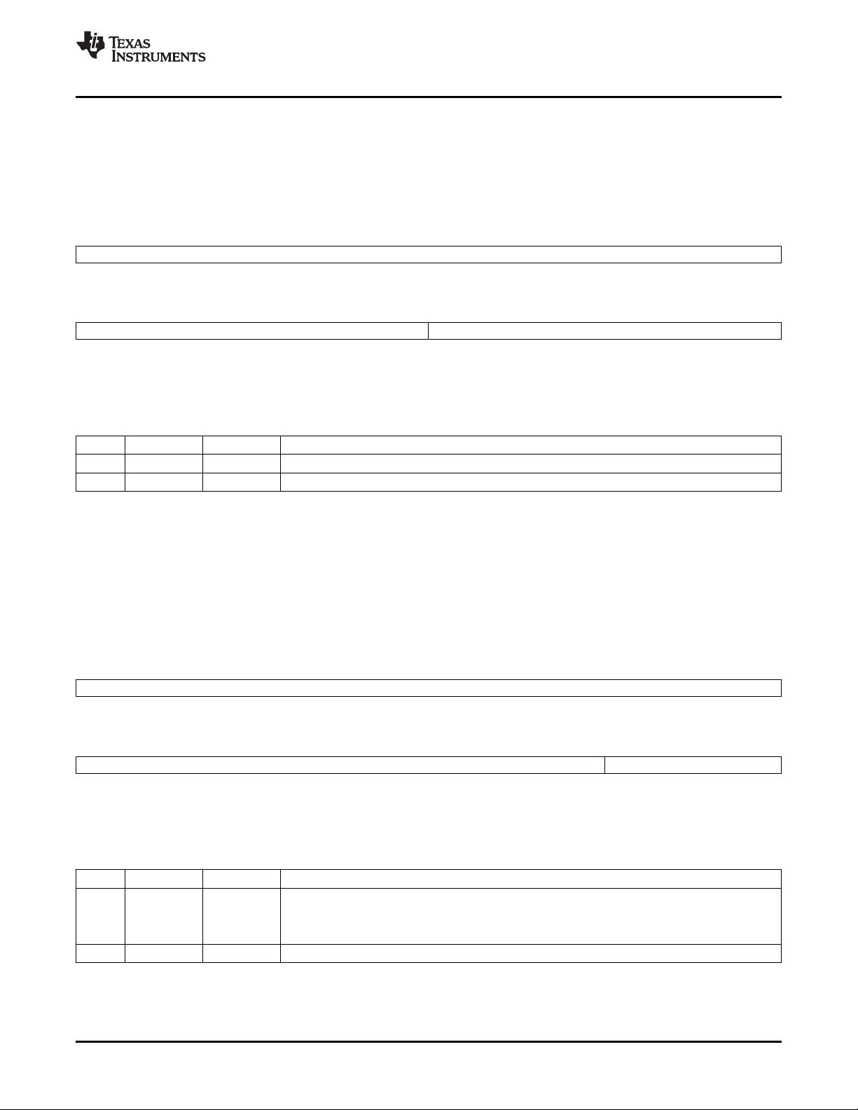
memory, as shown in .
2.7 Physical Addressing
Transactions on the internal bus use physical addresses, so all system memory accesses initiated by the
USB host controller must use physical addresses. The ARM CPU can be configured to use virtual
addressing. In this case, ARM side software manipulates virtual addresses that may or may not be
identical to physical addresses. When virtual addressing is used, system software must perform the
appropriate virtual address to physical address and physical address to virtual address conversions when
manipulating the USB host controllers data structures and pointers to those data structures.
Figure 1 shows the ARM virtual address to physical address conversion.
Figure 1. Relationships Between Virtual Address Physical Address
Architecture
SPRUFM8 – September 2008 Universal Serial Bus OHCI Host Controller 11
Submit Documentation Feedback
Page 12

Registers
www.ti.com
3 Registers
Most of the host controller (HC) registers are OHCI operational registers, defined by the OHCI
Specification for USB. Four additional registers not specified by the OHCI Specification for USB provide
additional information about the USB host controller state. USB host controller registers can be accessed
in user and supervisor modes.
To enhance code reusability with possible future versions of the USB host controller, reads and writes to
reserved USB host controller register addresses are to be avoided. Unless otherwise specified, when
writing registers that have reserved bits, read-modify-write operations must be used so that the reserved
bits are written with their previous values.
The USB host controller registers are listed in Table 1 .
Table 1. USB Host Controller Registers
Address Acronym Register Description Section
01E2 5000h HCREVISION OHCI Revision Number Register Section 3.1
01E2 5004h HCCONTROL HC Operating Mode Register Section 3.2
01E2 5008h HCCOMMANDSTATUS HC Command and Status Register Section 3.3
01E2 500Ch HCINTERRUPTSTATUS HC Interrupt and Status Register Section 3.4
01E2 5010h HCINTERRUPTENABLE HC Interrupt Enable Register Section 3.5
01E2 5014h HCINTERRUPTDISABLE HC Interrupt Disable Register Section 3.6
01E2 5018h HCHCCA HC HCAA Address Register
01E2 501Ch HCPERIODCURRENTED HC Current Periodic Register
01E2 5020h HCCONTROLHEADED HC Head Control Register
01E2 5024h HCCONTROLCURRENTED HC Current Control Register
01E2 5028h HCBULKHEADED HC Head Bulk Register
01E2 502Ch HCBULKCURRENTED HC Current Bulk Register
01E2 5030h HCDONEHEAD HC Head Done Register
01E2 5034h HCFMINTERVAL HC Frame Interval Register Section 3.14
01E2 5038h HCFMREMAINING HC Frame Remaining Register Section 3.15
01E2 503Ch HCFMNUMBER HC Frame Number Register Section 3.16
01E2 5040h HCPERIODICSTART HC Periodic Start Register Section 3.17
01E2 5044h HCLSTHRESHOLD HC Low-Speed Threshold Register Section 3.18
01E2 5048h HCRHDESCRIPTORA HC Root Hub A Register Section 3.19
01E2 504Ch HCRHDESCRIPTORB HC Root Hub B Register Section 3.20
01E2 5050h HCRHSTATUS HC Root Hub Status Register Section 3.21
01E2 5054h HCRHPORTSTATUS1 HC Port 1 Status and Control Register
01E2 5058h HCRHPORTSTATUS2 HC Port 2 Status and Control Register
(1)
(1)
(1)
(1)
(1)
(1)
(1)
(2)
(3)
Section 3.7
Section 3.8
Section 3.9
Section 3.10
Section 3.11
Section 3.12
Section 3.13
Section 3.22
Section 3.23
(1)
Restrictions apply to the physical addresses used in these registers (see Section 2.7 ).
(2)
Connected to the integrated USB1.1 phy pins (USB1_DM, USB1_DP).
(3)
Although the controller implements two ports, the second port cannot be used.
Universal Serial Bus OHCI Host Controller12 SPRUFM8 – September 2008
Submit Documentation Feedback
Page 13

www.ti.com
3.1 OHCI Revision Number Register (HCREVISION)
The OHCI revision number register (HCREVISION) is shown in Figure 2 and described in Table 2 .
Figure 2. OHCI Revision Number Register (HCREVISION)
31 16
Reserved
R-0
15 8 7 0
Reserved REV
R-0 R-10h
LEGEND: R = Read only; - n = value after reset
Table 2. OHCI Revision Number Register (HCREVISION) Field Descriptions
Bit Field Value Description
31-8 Reserved 0 Reserved
7-0 REV 10h OHCI revision number.
Registers
3.2 HC Operating Mode Register (HCCONTROL)
The HC operating mode register (HCCONTROL) controls the operating mode of the USB host controller.
HCCONTROL is shown in Figure 3 and described in Table 3 .
Figure 3. HC Operating Mode Register (HCCONTROL)
31 16
Reserved
R-0
15 11 10 9 8 7 6 5 4 3 2 1 0
Reserved RWE RWC IR HCFS BLE CLE IE PLE CBSR
R-0 R/W-0 R/W-0 R/W-0 R/W-0 R/W-0 R/W-0 R/W-0 R/W-0 R/W-0
LEGEND: R/W = Read/Write; R = Read only; - n = value after reset
SPRUFM8 – September 2008 Universal Serial Bus OHCI Host Controller 13
Submit Documentation Feedback
Page 14

Registers
Table 3. HC Operating Mode Register (HCCONTROL) Field Descriptions
Bit Field Value Description
31-11 Reserved 0 Reserved
10 RWE 0-1 Remote wake-up enable.
9 RWC 0-1 Remote wake-up connected.
8 IR 0 Interrupt routing. The USB host controller does not provide an SMI interrupt. This bit must be 0 to allow
the USB host controller interrupt to propagate to the MPU level 2 interrupt controller.
7-6 HCFS 0-3h Host controller functional state. A transition to USB operational causes SOF generation to begin in 1
ms. The USB host controller can automatically transition from USB suspend to USB resume, if a
downstream resume is received. The USB host controller enters USB suspend after a software reset.
The USB host controller enters USB reset after a hardware reset. The USB reset state resets the root
hub and causes downstream signaling of USB reset.
0 USB reset
1h USB resume
2h USB operational
3h USB suspend
5 BLE Bulk list enable.
0 The bulk ED list is not processed in the next 1 ms frame. The host controller driver can modify the bulk
ED list. If the driver removes the ED pointed to by the HC current bulk register (HCBULKCURRENTED)
from the ED list, it must update HCBULKCURRENTED to point to a current ED before it reenables the
bulk list.
1 Enables processing of the bulk ED list. The HC head bulk register (HCBULKHEADED) must be 0 or
point to a valid ED before setting this bit. The HC current bulk register (HCBULKCURRENTED) must be
0 or point to a valid ED before setting this bit.
4 CLE Control list enable.
0 The control ED list is not processed in the next 1 ms frame. The host controller driver can modify the
control ED list. If the driver removes the ED pointed to by the HC current control register
(HCCONTROLCURRENTED) from the ED list, it must update HCCONTROLCURRENTED to point to a
current ED before it reenables the control list.
1 Enables processing of the control ED list. The HC head control register (HCCONTROLHEADED) must
be 0 or point to a valid ED before setting this bit. The HC current control register
(HCCONTROLCURRENTED) must be 0 or point to a valid ED before setting this bit.
3 IE Isochronous enable.
0 Isochronous EDs are not processed. The USB host controller checks this bit every time it finds an
isochronous ED in the periodic list.
1 Enables processing of isochronous EDs in the next frame, if not in the current frame.
2 PLE Periodic list enable.
0 Periodic ED lists are not processed. Periodic list processing is disabled beginning with the next frame.
1 Enables processing of the periodic ED lists. Periodic list processing begins in the next frame.
1-0 CBSR 0-3h Control/bulk service ratio. Specifies the ratio between control and bulk EDs processed in a frame.
0 1 control ED per bulk ED.
1h 2 control EDs per bulk ED.
2h 3 control EDs per bulk ED.
3h 4 control EDs per bulk ED.
www.ti.com
Universal Serial Bus OHCI Host Controller14 SPRUFM8 – September 2008
Submit Documentation Feedback
Page 15

www.ti.com
3.3 HC Command and Status Register (HCCOMMANDSTATUS)
The HC command and status register (HCCOMMANDSTATUS) shows the current state of the host
controller and accepts commands from the host controller driver. HCCOMMANDSTATUS is shown in
Figure 4 and described in Table 4 .
Figure 4. HC Command and Status Register (HCCOMMANDSTATUS)
31 18 17 16
Reserved SOC
R-0 R-0
15 4 3 2 1 0
Reserved OCR BLF CLF HCR
R-0 R/W-0 R/W-0 R/W-0 R/W-0
LEGEND: R/W = Read/Write; R = Read only; - n = value after reset
Table 4. HC Command and Status Register (HCCOMMANDSTATUS) Field Descriptions
Bit Field Value Description
31-18 Reserved 0 Reserved
17-16 SOC 0-3h Scheduling overrun count. Counts the number of times a scheduling overrun occurs. This count is
incremented even if the host controller driver has not acknowledged any previous pending scheduling
overrun interrupt.
15-4 Reserved 0 Reserved
3 OCR 0-1 Ownership change request. The host controller driver sets this bit to gain ownership of the host
controller. The processor does not support SMI interrupts, so no ownership change interrupt occurs.
2 BLF 0-1 Bulk list filled. The host controller driver must set this bit if it modifies the bulk list to include new TDs. If
the HC current bulk register (HCBULKCURRENTED) is 0, the USB host controller does not begin
processing bulk list EDs unless this bit is set. When the USB host controller sees this bit set and begins
processing the bulk list, it clears this bit to 0.
1 CLF 0-1 Control list filled. The host controller driver must set this bit if it modifies the control list to include new
TDs. If the HC head control register (HCCONTROLHEADED) is 0, the USB host controller does not
begin processing control list EDs unless this bit is set. When the USB host controller sees this bit set
and begins processing the control list, it clears this bit to 0.
0 HCR Host controller reset.
0 No effect.
1 Initiates a software reset of the USB host controller. This transitions the USB host controller to the USB
suspend state. This resets most USB host controller OHCI registers. OHCI register accesses must not
be attempted until a read of this bit returns a 0. A write of 1 to this bit does not reset the root hub and
does not signal USB reset to downstream USB functions.
Registers
SPRUFM8 – September 2008 Universal Serial Bus OHCI Host Controller 15
Submit Documentation Feedback
Page 16

Registers
3.4 HC Interrupt and Status Register (HCINTERRUPTSTATUS)
The HC interrupt and status register (HCINTERRUPTSTATUS) reports the status of the USB host
controller internal interrupt sources. HCINTERRUPTSTATUS is shown in Figure 5 and described in
Table 5 .
Figure 5. HC Interrupt and Status Register (HCINTERRUPTSTATUS)
31 30 29 16
Rsvd OC Reserved
R-0 R-0 R-0
15 7 6 5 4 3 2 1 0
Reserved RHSC FNO UE RD SF WDH SO
R-0 R/W1C-0 R/W1C-0 R/W1C-0 R/W1C-0 R/W1C-0 R/W1C-0 R/W1C-0
LEGEND: R/W = Read/Write; R = Read only; W1C = Write 1 to clear (writing 0 has no effect); - n = value after reset
Table 5. HC Interrupt and Status Register (HCINTERRUPTSTATUS) Field Descriptions
Bit Field Value Description
31 Reserved 0 Reserved
30 OC 0-1 Ownership change.
29-7 Reserved 0 Reserved
6 RHSC Root hub status change. A write of 1 clears this bit; a write of 0 has no effect.
0 A root hub status change has not occurred.
1 A root hub status change has occurred.
5 FNO Frame number overflow. A write of 1 clears this bit; a write of 0 has no effect.
0 A frame number overflow has not occurred.
1 A frame number overflow has occurred.
4 UE Unrecoverable error. A write of 1 clears this bit; a write of 0 has no effect.
0 An unrecoverable error has not occurred.
1 An unrecoverable error has occurred on the OCPI bus, or that an isochronous TD PSW field condition
code was not set to Not Accessed when the USB host controller attempted to perform a transfer using
that PSW/offset pair.
3 RD Resume detected. A write of 1 clears this bit; a write of 0 has no effect.
0 A downstream device has not issued a resume request.
1 A downstream device has issued a resume request.
2 SF Start of frame. A write of 1 clears this bit; a write of 0 has no effect.
0 A SOF has not been issued.
1 A SOF has been issued.
1 WDH Write done head. The host controller driver must read the value from the HC head done register
(HCDONEHEAD) before writing 1 to this bit. A write of 1 clears this bit; a write of 0 has no effect.
0 USB host controller has not updated the HC head done register (HCDONEHEAD).
1 USB host controller has updated the HC head done register (HCDONEHEAD).
0 SO Scheduling overrun. A write of 1 clears this bit; a write of 0 has no effect.
0 A scheduling overrun has not occurred.
1 A scheduling overrun has occurred.
www.ti.com
16 Universal Serial Bus OHCI Host Controller SPRUFM8 – September 2008
Submit Documentation Feedback
Page 17

www.ti.com
3.5 HC Interrupt Enable Register (HCINTERRUPTENABLE)
The HC interrupt enable register (HCINTERRUPTENABLE) enables various OHCI interrupt sources to
generate interrupts to the level 2 interrupt controller. HCINTERRUPTENABLE is shown in Figure 6 and
described in Table 6 .
Figure 6. HC Interrupt Enable Register (HCINTERRUPTENABLE)
31 30 29 16
MIE OC Reserved
R/W1S-0 R-0 R-0
15 7 6 5 4 3 2 1 0
Reserved RHSC FNO UE RD SF WDH SO
R-0 R/W1S-0 R/W1S-0 R/W1S-0 R/W1S-0 R/W1S-0 R/W1S-0 R/W1S-0
LEGEND: R/W = Read/Write; R = Read only; W1S = Write 1 to set (writing 0 has no effect); - n = value after reset
Table 6. HC Interrupt Enable Register (HCINTERRUPTENABLE) Field Descriptions
Bit Field Value Description
31 MIE Master interrupt enable. A write of 1 sets this bit; a write of 0 has no effect. A write of 1 to the
corresponding bit in the HC interrupt disable register (HCINTERRUPTDISABLE) clears this bit.
0 OHCI interrupt sources are ignored and USB host controller interrupts are not propagated to the level 2
interrupt controller.
1 Allows other enabled OHCI interrupt sources to propagate to the level 2 interrupt controller.
30 OC 0-1 Ownership change.
29-7 Reserved 0 Reserved
6 RHSC Root hub status change. A write of 1 sets this bit; a write of 0 has no effect. A write of 1 to the
corresponding bit in the HC interrupt disable register (HCINTERRUPTDISABLE) clears this bit.
0 Root hub status change interrupts do not propagate.
1 When MIE is 1, allows root hub status change interrupts to propagate to the level 2 interrupt controller.
5 FNO Frame number overflow. A write of 1 sets this bit; a write of 0 has no effect. A write of 1 to the
corresponding bit in the HC interrupt disable register (HCINTERRUPTDISABLE) clears this bit.
0 Frame number overflow interrupts do not propagate.
1 When MIE is 1, allows frame number overflow interrupts to propagate to the level 2 interrupt controller.
4 UE Unrecoverable error. A write of 1 sets this bit; a write of 0 has no effect. A write of 1 to the
corresponding bit in the HC interrupt disable register (HCINTERRUPTDISABLE) clears this bit.
0 Unrecoverable error interrupts do not propagate.
1 When MIE is 1, allows unrecoverable error interrupts to propagate to the level 2 interrupt controller.
3 RD Resume detected. A write of 1 sets this bit; a write of 0 has no effect. A write of 1 to the corresponding
bit in the HC interrupt disable register (HCINTERRUPTDISABLE) clears this bit.
0 Resume detected interrupts do not propagate.
1 When MIE is 1, allows resume detected interrupts to propagate to the level 2 interrupt controller.
2 SF Start of frame. A write of 1 sets this bit; a write of 0 has no effect. A write of 1 to the corresponding bit in
the HC interrupt disable register (HCINTERRUPTDISABLE) clears this bit.
0 Start of frame interrupts do not propagate.
1 When MIE is 1, allows start of frame interrupts to propagate to the level 2 interrupt controller.
1 WDH Write done head. A write of 1 sets this bit; a write of 0 has no effect. A write of 1 to the corresponding
bit in the HC interrupt disable register (HCINTERRUPTDISABLE) clears this bit.
0 Write done head interrupts do not propagate.
1 When MIE is 1, allows write done head interrupts to propagate to the level 2 interrupt controller.
0 SO Scheduling overrun. A write of 1 sets this bit; a write of 0 has no effect. A write of 1 to the corresponding
bit in the HC interrupt disable register (HCINTERRUPTDISABLE) clears this bit.
0 Scheduling overrun interrupts do not propagate.
1 When MIE is 1, allows scheduling overrun interrupts to propagate to the level 2 interrupt controller.
Registers
SPRUFM8 – September 2008 Universal Serial Bus OHCI Host Controller 17
Submit Documentation Feedback
Page 18

Registers
3.6 HC Interrupt Disable Register (HCINTERRUPTDISABLE)
The HC interrupt disable register (HCINTERRUPTDISABLE) is used to clear bits in the HC interrupt
enable register (HCINTERRUPTENABLE). HCINTERRUPTDISABLE is shown in Figure 7 and described
in Table 7 .
Figure 7. HC Interrupt Disable Register (HCINTERRUPTDISABLE)
31 30 29 16
MIE OC Reserved
R/W-0 R-0 R-0
15 7 6 5 4 3 2 1 0
Reserved RHSC FNO UE RD SF WDH SO
R-0 R/W-0 R/W-0 R/W-0 R/W-0 R/W-0 R/W-0 R/W-0
LEGEND: R/W = Read/Write; R = Read only; - n = value after reset
Table 7. HC Interrupt Disable Register (HCINTERRUPTDISABLE) Field Descriptions
Bit Field Value Description
31 MIE Master interrupt enable. Read always returns 0.
0 No effect.
1 Clears the MIE bit in the HC interrupt enable register (HCINTERRUPTENABLE).
30 OC 0-1 Ownership change.
29-7 Reserved 0 Reserved
6 RHSC Root hub status change. Read always returns 0.
0 No effect.
1 Clears the RHSC bit in the HC interrupt enable register (HCINTERRUPTENABLE).
5 FNO Frame number overflow. Read always returns 0.
0 No effect.
1 Clears the FNO bit in the HC interrupt enable register (HCINTERRUPTENABLE).
4 UE Unrecoverable error. Read always returns 0.
0 No effect.
1 Clears the UE bit in the HC interrupt enable register (HCINTERRUPTENABLE).
3 RD Resume detected. Read always returns 0.
0 No effect.
1 Clears the RD bit in the HC interrupt enable register (HCINTERRUPTENABLE).
2 SF Start of frame. Read always returns 0.
0 No effect.
1 Clears the SF bit in the HC interrupt enable register (HCINTERRUPTENABLE).
1 WDH Write done head. Read always returns 0.
0 No effect.
1 Clears the WDH bit in the HC interrupt enable register (HCINTERRUPTENABLE).
0 SO Scheduling overrun. Read always returns 0.
0 No effect.
1 Clears the SO bit in the HC interrupt enable register (HCINTERRUPTENABLE).
www.ti.com
Universal Serial Bus OHCI Host Controller18 SPRUFM8 – September 2008
Submit Documentation Feedback
Page 19
www.ti.com
3.7 HC HCAA Address Register (HCHCCA)
The HC HCAA address register (HCHCCA) defines the physical address of the beginning of the HCCA.
HCHCCA is shown in Figure 8 and described in Table 8 .
Figure 8. HC HCAA Address Register (HCHCCA)
31 16
HCCA
R/W-0
15 8 7 0
HCCA Reserved
R/W-0 R-0
LEGEND: R/W = Read/Write; R = Read only; - n = value after reset
Table 8. HC HCAA Address Register (HCHCCA) Field Descriptions
Bit Field Value Description
31-8 HCCA 0-FF FFFFh Physical address of the beginning of the HCCA.
7-0 Reserved 0 Reserved
Registers
3.8 HC Current Periodic Register (HCPERIODCURRENTED)
The HC current periodic register (HCPERIODCURRENTED) defines the physical address of the next
endpoint descriptor (ED) on the periodic ED list. HCPERIODCURRENTED is shown in Figure 9 and
described in Table 9 .
Figure 9. HC Current Periodic Register (HCPERIODCURRENTED)
31 16
PCED
R-0
15 4 3 0
PCED Reserved
R-0 R-0
LEGEND: R = Read only; - n = value after reset
Table 9. HC Current Periodic Register (HCPERIODCURRENTED) Field Descriptions
Bit Field Value Description
31-4 PCED 0-FFF FFFFh Physical address of the current ED on the periodic ED list. This field represents bits 31-4 of the
3-0 Reserved 0 Reserved
physical address of the next ED on the periodic ED list. EDs are assumed to begin on a 16-byte
aligned address, so bits 3-0 of this pointer are assumed to be 0. For the restrictions on physical
addresses, see Section 2.7 .
SPRUFM8 – September 2008 Universal Serial Bus OHCI Host Controller 19
Submit Documentation Feedback
Page 20

Registers
3.9 HC Head Control Register (HCCONTROLHEADED)
The HC head control register (HCCONTROLHEADED) defines the physical address of the head endpoint
descriptor (ED) on the control ED list. HCCONTROLHEADED is shown in Figure 10 and described in
Table 10 .
Figure 10. HC Head Control Register (HCCONTROLHEADED)
31 16
CHED
R/W-0
15 4 3 0
CHED Reserved
R/W-0 R-0
LEGEND: R/W = Read/Write; R = Read only; - n = value after reset
Table 10. HC Head Control Register (HCCONTROLHEADED) Field Descriptions
Bit Field Value Description
31-4 CHED 0-FFF FFFFh Physical address of the head ED on the control ED list. This field represents bits 31-4 of the
physical address of the head ED on the control ED list. EDs are assumed to begin on a 16-byte
aligned address, so bits 3-0 of this pointer are assumed to be 0. For the restrictions on physical
addresses, see Section 2.7 .
3-0 Reserved 0 Reserved
www.ti.com
20 Universal Serial Bus OHCI Host Controller SPRUFM8 – September 2008
Submit Documentation Feedback
Page 21

www.ti.com
3.10 HC Current Control Register (HCCONTROLCURRENTED)
The HC current control register (HCCONTROLCURRENTED) defines the physical address of the next
endpoint descriptor (ED) on the control ED list. HCCONTROLCURRENTED is shown in Figure 11 and
described in Table 11 .
Figure 11. HC Current Control Register (HCCONTROLCURRENTED)
31 16
CCED
R/W-0
15 4 3 0
CCED Reserved
R/W-0 R-0
LEGEND: R/W = Read/Write; R = Read only; - n = value after reset
Table 11. HC Current Control Register (HCCONTROLCURRENTED) Field Descriptions
Bit Field Value Description
31-4 CCED 0-FFF FFFFh Physical address of the current ED on the control ED list. This field represents bits 31-4 of the
physical address of the next ED on the control ED list. EDs are assumed to begin on a 16-byte
aligned address, so bits 3-0 of this pointer are assumed to be 0. For the restrictions on physical
addresses, see Section 2.7 .
A value of 0 indicates that the USB host controller has reached the end of the control ED list
without finding any transfers to process. This register is automatically updated by the USB host
controller.
3-0 Reserved 0 Reserved
Registers
SPRUFM8 – September 2008 Universal Serial Bus OHCI Host Controller 21
Submit Documentation Feedback
Page 22

Registers
3.11 HC Head Bulk Register (HCBULKHEADED)
The HC head bulk register (HCBULKHEADED) defines the physical address of the head endpoint
descriptor (ED) on the bulk ED list. HCBULKHEADED is shown in Figure 12 and described in Table 12 .
Figure 12. HC Head Bulk Register (HCBULKHEADED)
31 16
BHED
R/W-0
15 4 3 0
BHED Reserved
R/W-0 R-0
LEGEND: R/W = Read/Write; R = Read only; - n = value after reset
Table 12. HC Head Bulk Register (HCBULKHEADED) Field Descriptions
Bit Field Value Description
31-4 BHED 0-FFF FFFFh Physical address of the head ED on the bulk ED list. This field represents bits 31-4 of the physical
address of the head ED on the bulk ED list. EDs are assumed to begin on a 16-byte aligned
address, so bits 3-0 of this pointer are assumed to be 0. For the restrictions on physical
addresses, see Section 2.7 .
3-0 Reserved 0 Reserved
www.ti.com
3.12 HC Current Bulk Register (HCBULKCURRENTED)
The HC current bulk register (HCBULKCURRENTED) defines the physical address of the next endpoint
descriptor (ED) on the bulk ED list. HCBULKCURRENTED is shown in Figure 13 and described in
Table 13 .
Figure 13. HC Current Bulk Register (HCBULKCURRENTED)
31 16
BCED
R/W-0
15 4 3 0
BCED Reserved
R/W-0 R-0
LEGEND: R/W = Read/Write; R = Read only; - n = value after reset
Table 13. HC Current Bulk Register (HCBULKCURRENTED) Field Descriptions
Bit Field Value Description
31-4 BCED 0-FFF FFFFh Physical address of the current ED on the bulk ED list. This field represents bits 31-4 of the
3-0 Reserved 0 Reserved
physical address of the next ED on the bulk ED list. EDs are assumed to begin on a 16-byte
aligned address, so bits 3-0 of this pointer are assumed to be 0. For the restrictions on physical
addresses, see Section 2.7 .
A value of 0 indicates that the USB host controller has reached the end of the bulk ED list without
finding any transfers to process. This register is automatically updated by the USB host controller.
Universal Serial Bus OHCI Host Controller22 SPRUFM8 – September 2008
Submit Documentation Feedback
Page 23

www.ti.com
3.13 HC Head Done Register (HCDONEHEAD)
The HC head done register (HCDONEHEAD) defines the physical address of the current head of the done
TD queue. HCDONEHEAD is shown in Figure 14 and described in Table 14 .
Figure 14. HC Head Done Register (HCDONEHEAD)
31 16
DH
R-0
15 4 3 0
DH Reserved
R-0 R-0
LEGEND: R = Read only; - n = value after reset
Table 14. HC Head Done Register (HCDONEHEAD) Field Descriptions
Bit Field Value Description
31-4 DH 0-FFF FFFFh Physical address of the last TD that has added to the done queue. This field represents bits 31-4
of the physical address of the top TD on the done TD queue. TDs are assumed to begin on a
16-byte aligned address, so bits 3-0 of this pointer are assumed to be 0.
A value of 0 indicates that there are no TDs on the done queue. This register is automatically
updated by the USB host controller.
3-0 Reserved 0 Reserved
Registers
3.14 HC Frame Interval Register (HCFMINTERVAL)
The HC frame interval register (HCFMINTERVAL) defines the number of 12-MHZ clock pulses in each
USB frame. HCFMINTERVAL is shown in Figure 15 and described in Table 15 .
Figure 15. HC Frame Interval Register (HCFMINTERVAL)
31 30 16
FIT FSMPS
R/W-0 R/W-0
15 14 13 0
Reserved FRAMEINTERVAL
R-0 R/W-2EDFh
LEGEND: R/W = Read/Write; R = Read only; - n = value after reset
Table 15. HC Frame Interval Register (HCFMINTERVAL) Field Descriptions
Bit Field Value Description
31 FIT 0-1 Frame interval toggle. The host controller driver must toggle this bit any time it changes
30-16 FSMPS 0-7FFFh Largest data packet. Largest data packet size allowed for full-speed packets, in bit times.
15-14 Reserved 0 Reserved
13-0 FRAMEINTERVAL 0-3FFFh Frame interval. Number of 12-MHZ clocks in the USB frame. Nominally, this is set to
the frame interval field.
11,999 (2EDFh) to give a 1-ms frame. The host controller driver can make minor changes
to this field to attempt to manually synchronize with another clock source.
SPRUFM8 – September 2008 Universal Serial Bus OHCI Host Controller 23
Submit Documentation Feedback
Page 24

Registers
3.15 HC Frame Remaining Register (HCFMREMAINING)
The HC frame remaining register (HCFMREMAINING) reports the number of full-speed bit times
remaining in the current frame. HCFMREMAINING is shown in Figure 16 and described in Table 16 .
Figure 16. HC Frame Remaining Register (HCFMREMAINING)
31 30 16
FRT Reserved
R-0 R-0
15 14 13 0
Reserved FR
R-0 R-0
LEGEND: R = Read only; - n = value after reset
Table 16. HC Frame Remaining Register (HCFMREMAINING) Field Descriptions
Bit Field Value Description
31 FRT 0-1 Frame remaining toggle. This bit is loaded with the frame interval toggle bit every time the USB
host controller loads the frame interval field into the frame remaining field.
30-14 Reserved 0 Reserved
13-0 FR 0-3FFFh Frame remaining. The number of full-speed bit times remaining in the current frame. This field is
automatically reloaded with the frame interval (FI) value in the HC frame interval register
(HCFMINTERVAL) at the beginning of every frame.
www.ti.com
3.16 HC Frame Number Register (HCFMNUMBER)
The HC frame number register (HCFMNUMBER) reports the current USB frame number. HCFMNUMBER
is shown in Figure 17 and described in Table 17 .
Figure 17. HC Frame Number Register (HCFMNUMBER)
31 16
Reserved
R-0
15 0
FN
R-0
LEGEND: R = Read only; - n = value after reset
Table 17. HC Frame Number Register (HCFMNUMBER) Field Descriptions
Bit Field Value Description
31-16 Reserved 0 Reserved
15-0 FN 0-FFFFh Frame number. This field reports the current USB frame number. It is incremented when the frame
remaining field is reloaded with the frame interval (FI) value in the HC frame interval register
(HCFMINTERVAL). Frame number automatically rolls over from FFFFh to 0. After frame number is
incremented, its new value is written to the HCCA and the USB host controller sets the SOF
interrupt status bit and begins processing the ED lists.
Universal Serial Bus OHCI Host Controller24 SPRUFM8 – September 2008
Submit Documentation Feedback
Page 25

www.ti.com
3.17 HC Periodic Start Register (HCPERIODICSTART)
The HC periodic start register (HCPERIODICSTART) defines the position within the USB frame where
endpoint descriptors (EDs) on the periodic list have priority over EDs on the bulk and control lists.
HCPERIODICSTART is shown in Figure 18 and described in Table 18 .
Figure 18. HC Periodic Start Register (HCPERIODICSTART)
31 16
Reserved
R-0
15 14 13 0
Reserved PS
R-0 R/W-0
LEGEND: R/W = Read/Write; R = Read only; - n = value after reset
Table 18. HC Periodic Start Register (HCPERIODICSTART) Field Descriptions
Bit Field Value Description
31-14 Reserved 0 Reserved
13-0 PS 0-3FFFh Periodic start. The host controller driver must program this value to be about 10% less than the
frame interval (FI) value in the HC frame interval register (HCFMINTERVAL), so that control and
bulk EDs have priority for the first 10% of the frame; then periodic EDs have priority for the
remaining 90% of the frame.
Registers
SPRUFM8 – September 2008 Universal Serial Bus OHCI Host Controller 25
Submit Documentation Feedback
Page 26

Registers
3.18 HC Low-Speed Threshold Register (HCLSTHRESHOLD)
The HC low-speed threshold register (HCLSTHRESHOLD) defines the latest time in a frame that the USB
host controller can begin a low-speed packet. HCLSTHRESHOLD is shown in Figure 19 and described in
Table 19 .
Figure 19. HC Low-Speed Threshold Register (HCLSTHRESHOLD)
31 16
Reserved
R-0
15 14 13 0
Reserved LST
R-0 R/W-628h
LEGEND: R/W = Read/Write; R = Read only; - n = value after reset
Table 19. HC Low-Speed Threshold Register (HCLSTHRESHOLD) Field Descriptions
Bit Field Value Description
31-14 Reserved 0 Reserved
13-0 LST 0-3FFFh Low-speed threshold. This field defines the number of full-speed bit times in the frame after which
the USB host controller cannot start an 8-byte low-speed packet. The USB host controller only
begins a low-speed transaction if the frame remaining (FR) value in the HC frame remaining
register (HCFMREMAINING) is greater than the low-speed threshold.
The host controller driver must set this field to a value that ensures that an 8-byte low-speed TD
completes before the end of the frame. When set, the host controller driver must not change the
value.
www.ti.com
Universal Serial Bus OHCI Host Controller26 SPRUFM8 – September 2008
Submit Documentation Feedback
Page 27

www.ti.com
3.19 HC Root Hub A Register (HCRHDESCRIPTORA)
The HC root hub A register (HCRHDESCRIPTORA) defines several aspects of the USB host controller
root hub functionality. HCRHDESCRIPTORA is shown in Figure 20 and described in Table 20 .
Figure 20. HC Root Hub A Register (HCRHDESCRIPTORA)
31 24 16
POTPG Reserved
R/W-Ah R-0
15 13 12 11 10 9 8 7 0
Reserved NOCP OCPM DT NPS PSM NDP
R-0 R/W-1 R/W-0 R-0 R/W-1 R/W-0 R-3h
LEGEND: R/W = Read/Write; R = Read only; - n = value after reset
Table 20. HC Root Hub A Register (HCRHDESCRIPTORA) Field Descriptions
Bit Field Value Description
31-24 POTPG 0-FFh Power-on to power-good time. Defines the minimum amount of time (2 ms × POTPG) between the USB
host controller turning on power to a downstream port and when the USB host can access the
downstream device. This field has no effect on USB host controller operation. After turning on power to
a port, the USB host controller driver must delay the amount of time implied by POTPG before
attempting to reset an attached downstream device. The required amount of time is
implementation-specific and must be calculated based on the amount of time the VBUS supply takes to
provide valid VBUS to a worst-case downstream USB function controller. The implementation-specific
value must be computed and then written to this register before the USB host controller driver is
initialized. Because the device does not provide a direct control from the USB host controller to switch
VBUS on and off, this value must take into account any delays caused by other methods of controlling
VBUS externally. This field has no relationship to the OTG controller register bits that relate to VBUS.
System software can update this register to simplify host controller driver and/or OTG driver coding.
23-13 Reserved 0 Reserved
12 NOCP 1 No overcurrent protection. Because the device does not provide signals to allow connection of external
overcurrent indication signals to the USB host controller, this bit defaults to 1 that indicates that the USB
host controller does not implement overcurrent protection inputs. This bit has no relationship to the OTG
controller register bits that relate to VBUS.
11 OCPM 0 Overcurrent protection mode. Because the device does not provide host controller overcurrent
protection input signals, this bit has no effect. This bit has no relationship to the OTG controller register
bits that relate to VBUS.
10 DT 0 Device type. This bit is always 0, which indicates that the USB host controller implemented is not a
compound device.
9 NPS 1 No power switching. Because the device does not provide connections from the USB host controller to
control external VBUS switching, this bit defaults to 1 that indicates that VBUS power switching is not
supported and that power is available to all downstream ports when the USB host controller is powered.
This bit has no relationship to the OTG controller register bits that relate to VBUS. System software can
update this register to simplify host controller driver and/or OTG driver coding.
8 PSM 0 Power switching mode. Because the device does not provide signals from the USB host controller to
control external VBUS switching, this bit defaults to 0 that indicates that all ports are powered at the
same time.
7-0 NDP 0-FFh Number of downstream ports. The USB signal multiplexing mode and top-level pin multiplexing features
can place the device in a mode where 0, 1, 2, or 3 of the USB host controller downstream ports are
usable. This register reports three ports, regardless of USB signal multiplexing mode and top-level pin
multiplexing mode.
Registers
SPRUFM8 – September 2008 Universal Serial Bus OHCI Host Controller 27
Submit Documentation Feedback
Page 28

Registers
3.20 HC Root Hub B Register (HCRHDESCRIPTORB)
The HC root hub B register (HCRHDESCRIPTORB) defines several aspects of the USB host controller
root hub functionality. HCRHDESCRIPTORB is shown in Figure 21 and described in Table 21 .
Note: The device does not provide connections from the USB host controller to pins to provide
external port power switching. Systems that implement port power switching must use other
mechanisms to control port power.
Figure 21. HC Root Hub B Register (HCRHDESCRIPTORB)
31 20 19 18 17 16
PPCM[15-4] PPCM[3] PPCM[2] PPCM[1] PPCM[0]
R/W-0 R/W-0 R/W-0 R/W-0 R/W-0
15 4 3 2 1 0
DR[15-4] DR[3] DR[2] DR[1] DR[0]
R/W-0 R/W-0 R/W-0 R/W-0 R/W-0
LEGEND: R/W = Read/Write; - n = value after reset
Table 21. HC Root Hub B Register (HCRHDESCRIPTORB) Field Descriptions
Bit Field Value Description
31-20 PPCM[15-4] 0 Port power control mask. PPCM[15] through PPCM[4] are reserved.
19 PPCM[3] Port power control mask. PPCM[3] is the port power control mask for downstream port 3. Defines
whether downstream port 3 has port power controlled by the global power control. System software can
update these bits to simplify host controller driver and/or OTG driver coding.
0 Global power control is implemented for downstream port 3.
1 Per-port power control is implemented for downstream port 3.
18 PPCM[2] Port power control mask. PPCM[2] is the port power control mask for downstream port 2. Defines
whether downstream port 2 has port power controlled by the global power control. System software can
update these bits to simplify host controller driver and/or OTG driver coding.
0 Global power control is implemented for downstream port 2.
1 Per-port power control is implemented for downstream port 2.
17 PPCM[1] Port power control mask. PPCM[1] is the port power control mask for downstream port 1. Defines
whether downstream port 1 has port power controlled by the global power control. System software can
update these bits to simplify host controller driver and/or OTG driver coding.
0 Global power control is implemented for downstream port 1.
1 Per-port power control is implemented for downstream port 1.
16 PPCM[0] 0 Port power control mask. PPCM[0] is reserved.
15-4 DR[15-4] 0 Device removable. DR[15] through DR[4] are reserved.
3 DR[3] Device removable. DR[3] is the device removable bit for downstream port 3. Defines whether
downstream port 3 has a removable or nonremovable device.
0 Downstream port 3 may have a removable device attached.
1 Downstream port 3 has a nonremovable device attached.
2 DR[2] Device removable. DR[2] is the device removable bit for downstream port 2. Defines whether
downstream port 2 has a removable or nonremovable device.
0 Downstream port 2 may have a removable device attached.
1 Downstream port 2 has a nonremovable device attached.
1 DR[1] Device removable. DR[1] is the device removable bit for downstream port 1. Defines whether
downstream port 1 has a removable or nonremovable device.
0 Downstream port 1 may have a removable device attached.
1 Downstream port 1 has a nonremovable device attached.
0 DR[0] 0 Device removable. DR[0] is reserved.
www.ti.com
Universal Serial Bus OHCI Host Controller28 SPRUFM8 – September 2008
Submit Documentation Feedback
Page 29

www.ti.com
3.21 HC Root Hub Status Register (HCRHSTATUS)
The HC root hub status register (HCRHSTATUS) reports the USB host controller root hub status.
HCRHSTATUS is shown in Figure 22 and described in Table 22 .
Figure 22. HC Root Hub Status Register (HCRHSTATUS)
31 30 18 17 16
CRWE Reserved OCIC LPSC
R/W-0 R-0 R/W-0 R/W-0
15 14 2 1 0
DRWE Reserved OCI LPS
R/W-0 R-0 R-0 R/W-0
LEGEND: R/W = Read/Write; R = Read only; - n = value after reset
Table 22. HC Root Hub Status Register (HCRHSTATUS) Field Descriptions
Bit Field Value Description
31 CRWE Clear remote wake-up enable.
0 No effect..
1 Clears the device remote wake-up enable bit.
30-18 Reserved 0 Reserved
17 OCIC Overcurrent indication change. This bit is automatically set when the overcurrent indicator bit changes.
This bit has no relationship to the OTG controller register bits that relate to VBUS. System software can
update this register to simplify host controller driver and/or OTG driver coding.
0 No effect.
1 Clears this bit.
16 LPSC 0 Local power status change. Because the root hub does not support the local power status feature, this
bit defaults to 0 and has no effect. This bit has no relationship to the OTG controller register bits that
relate to VBUS. System software can update this register to simplify host controller driver and/or OTG
driver coding.
15 DRWE Device remote wake-up enable.
When 1, this bit enables a connect status change event to be treated as a resume event, which causes
a transition from USB suspend to USB resume state and sets the resume detected interrupt status bit.
When 0, connect status change events do not cause a transition from USB suspend to USB resume
state and the resume detected interrupt is not changed.
0 A write of 0 has no effect.
1 A write of 1 sets the device remote wake-up enable bit.
14-2 Reserved 0 Reserved
1 OCI 0 Overcurrent indicator. Because the device does not provide signals for external hardware to report
overcurrent status to the USB host controller, this bit is always 0. This bit has no relationship to the
OTG controller register bits that relate to VBUS.
0 LPS 0 Local power status. Because the root hub does not support the local power status feature, this bit
defaults to 0 and has no effect. This bit has no relationship to the OTG controller register bits that relate
to VBUS. System software can update this register to simplify host controller driver and/or OTG driver
coding.
Registers
SPRUFM8 – September 2008 Universal Serial Bus OHCI Host Controller 29
Submit Documentation Feedback
Page 30

Registers
3.22 HC Port 1 Status and Control Register (HCRHPORTSTATUS1)
The HC port 1 status and control register (HCRHPORTSTATUS1) reports and controls the state of USB
host port 1. HCRHPORTSTATUS1 is shown in Figure 23 and described in Table 23 .
Figure 23. HC Port 1 Status and Control Register (HCRHPORTSTATUS1)
31 21 20 19 18 17 16
Reserved PRSC OCIC PSSC PESC CSC
R-0 R/W1C-0 R/W-0 R/W1C-0 R/W1C-0 R/W1C-0
15 10 9 8
Reserved LSDA/CPP PPS/SPP
R-0 R/W-0 R/W-1
7 5 4 3 2 1 0
Reserved PRS/SPR POCI/CSS PSS/SPS PES/SPE CCS/CPE
R-0 R/W-0 R/W-0 R/W-0 R/W-0 R/W-0
LEGEND: R/W = Read/Write; R = Read only; W1C = Write 1 to clear (writing 0 has no effect); - n = value after reset
Table 23. HC Port 1 Status and Control Register (HCRHPORTSTATUS1) Field Descriptions
Bit Field Value Description
31-21 Reserved 0 Reserved
20 PRSC Port 1 reset status change. A write of 1 clears this bit; a write of 0 has no effect.
0 Port 1 port reset status bit has not changed.
1 Port 1 port reset status bit has changed.
19 OCIC 0 Port 1 overcurrent indicator change. Because the device does not provide inputs for signaling
external overcurrent indication to the USB host controller, this bit is always 0. Overcurrent
monitoring, if required, must be handled through some other mechanism. This bit has no
relationship to the OTG controller register bits that relate to VBUS.
18 PSSC Port 1 suspend status change. A write of 1 clears this bit; a write of 0 has no effect.
0 Port 1 port suspend status has not changed.
1 Port 1 port suspend status has changed. Suspend status is considered to have changed only after
the resume pulse, low-speed EOP, and 3-ms synchronization delays have been completed.
17 PESC Port 1 enable status change. A write of 1 clears this bit; a write of 0 has no effect.
0 Port 1 port enable status has not changed.
1 Port 1 port enable status has changed.
16 CSC Port 1 connect status change. If the DR[1] bit in the HC root hub B register (HCRHDESCRIPTORB)
is set to 1 to indicate a nonremovable USB device on port 1, this bit is set only after a root hub
reset to inform the system that the device is attached. A write of 1 clears this bit; a write of 0 has no
effect.
0 Port 1 current connect status has not changed.
1 Port 1 current connect status has changed due to a connect or disconnect event. If current connect
status is 0 when a set port reset, set port enable, or set port suspend write occurs, then this bit is
set.
15-10 Reserved 0 Reserved
9 LSDA/CPP Port 1 low-speed device attached/clear port power. This bit is valid only when port 1 current
connect status is 1. The host controller driver can write a 1 to this bit to clear the port 1 port power
status bit; a write of 0 has no effect. The USB host controller does not control external port power
using OHCI mechanisms, so, if required, USB host port power must be controlled through other
means. This bit has no relationship to the OTG controller register bits that relate to VBUS. System
software can update this register to simplify host controller driver and/or OTG driver coding.
0 Full-speed device is attached to port 1.
1 Low-speed device is attached to port 1.
www.ti.com
30 Universal Serial Bus OHCI Host Controller SPRUFM8 – September 2008
Submit Documentation Feedback
Page 31

www.ti.com
Table 23. HC Port 1 Status and Control Register (HCRHPORTSTATUS1) Field Descriptions (continued)
Bit Field Value Description
8 PPS/SPP Port 1 port power status/set port power. The host controller driver can write a 1 to this bit to set the
port 1 port power status bit; a write of 0 has no effect. The device does not provide signals from the
USB host controller to control external port power, so if required, USB host port power control
signals must be controlled through other means. Software can track the current power state using
the port power status bit and other power control bits, but those bits have no direct effect on
external port power control. This bit has no relationship to the OTG controller register bits that relate
to VBUS. System software can update this register to simplify host controller driver and/or OTG
driver coding.
0 Port 1 power is disabled.
1 Port 1 power is enabled.
7-5 Reserved 0 Reserved
4 PRS/SPR Port 1 port reset status/set port reset. A write of 1 to this bit sets the port 1 port reset status bit and
causes the USB host controller to begin signaling USB reset to port 1; a write of 0 has no effect.
0 USB reset is not being sent to port 1.
1 Port 1 is signaling the USB reset.
3 POCI/CSS Port 1 port overcurrent indicator/clear suspend status. A write of 1 to this bit when port 1 port
suspend status is 1 causes resume signaling on port 1; a write of 1 when port 1 port suspend
status is 0 has no effect; a write of 0 has no effect. The device does not provide inputs for signaling
external overcurrent indication to the USB host controller. Overcurrent monitoring, if required, must
be handled through some other mechanism.
0 Port 1 port overcurrent condition has not occurred.
1 Port 1 port overcurrent condition has occurred.
2 PSS/SPS Port 1 port suspend status/set port suspend. A write of 1 to this bit when port 1 current connect
status is 1 sets the port 1 port suspend status bit and places port 1 in USB suspend state; a write of
1 when port 1 current connect status is 0 sets the connect status change to inform the USB host
controller driver software of an attempt to suspend a disconnected device; a write of 0 has no
effect. This bit is cleared automatically at the end of the USB resume sequence and also at the end
of the USB reset sequence.
0 Port 1 is not in the USB suspend state.
1 Port 1 is in the USB suspend state or is in the resume sequence.
1 PES/SPE Port 1 port enable status/set port enable. A write of 1 to this bit when port 1 current connect status
is 1 sets the port 1 port enable status bit; a write of 1 when port 1 current connect status is 0 has no
effect; a write of 0 has no effect. This bit is automatically set at completion of port 1 USB reset, if it
was not already set before the USB reset completed; and this bit is automatically set at the end of a
USB suspend, if the port was not enabled when the USB resume completed.
0 Port 1 is disabled.
1 Port 1 is enabled.
0 CCS/CPE Port 1 current connection status/clear port enable. If the DR[1] bit in the HC root hub B register
(HCRHDESCRIPTORB) is set to 1 to indicate a nonremovable USB device on port 1, this bit is set
after a root hub reset to inform the system that the device is attached. A write of 1 clears this bit; a
write of 0 has no effect.
0 No USB device is attached to port 1.
1 USB device is attached to port 1.
Registers
SPRUFM8 – September 2008 Universal Serial Bus OHCI Host Controller 31
Submit Documentation Feedback
Page 32

Registers
3.23 HC Port 2 Status and Control Register (HCRHPORTSTATUS2)
The HC port 2 status and control register (HCRHPORTSTATUS2) reports and controls the state of USB
host port 2. HCRHPORTSTATUS2 is shown in Figure 24 and described in Table 24 .
Figure 24. HC Port 2 Status and Control Register (HCRHPORTSTATUS2)
31 21 20 19 18 17 16
Reserved PRSC OCIC PSSC PESC CSC
R-0 R/W1C-0 R/W-0 R/W1C-0 R/W1C-0 R/W-0
15 10 9 8
Reserved LSDA/CPP PPS/SPP
R-0 R/W-0 R/W-1
7 5 4 3 2 1 0
Reserved PRS/SPR POCI/CSS PSS/SPS PES/SPE CCS/CPE
R-0 R/W-0 R/W-0 R/W-0 R/W-0 R/W-0
LEGEND: R/W = Read/Write; R = Read only; W1C = Write 1 to clear (writing 0 has no effect); - n = value after reset
Table 24. HC Port 2 Status and Control Register (HCRHPORTSTATUS2) Field Descriptions
Bit Field Value Description
31-21 Reserved 0 Reserved
20 PRSC Port 2 reset status change. A write of 1 clears this bit; a write of 0 has no effect.
0 Port 2 port reset status bit has not changed.
1 Port 2 port reset status bit has changed.
19 OCIC 0 Port 2 overcurrent indicator change. Because the device does not provide inputs for signaling
external overcurrent indication to the USB host controller, this bit is always 0. Overcurrent
monitoring, if required, must be handled through some other mechanism. This bit has no
relationship to the OTG controller register bits that relate to VBUS.
18 PSSC Port 2 suspend status changed. A write of 1 clears this bit; a write of 0 has no effect.
0 Port 2 port suspend status has not changed.
1 Port 2 port suspend status has changed. Suspend status is considered to have changed only after
the resume pulse, low-speed EOP, and 3-ms synchronization delays have been completed.
17 PESC Port 2 enable status change. A write of 1 clears this bit; a write of 0 has no effect.
0 Port 2 port enable status has not changed.
1 Port 2 port enable status has changed.
16 CSC Port 2 connect status change. If the DR[2] bit in the HC root hub B register (HCRHDESCRIPTORB)
is set to 1 to indicate a nonremovable USB device on port 2, this bit is set only after a root hub
reset to inform the system that the device is attached. A write of 1 clears this bit; a write of 0 has no
effect.
0 Port 2 current connect status has not changed.
1 Port 2 current connect status has changed due to a connect or disconnect event. If current connect
status is 0 when a set port reset, set port enable, or set port suspend write occurs, then this bit is
set.
15-10 Reserved 0 Reserved
9 LSDA/CPP Port 2 low-speed device attached/clear port power. This bit indicates, when read as 1, that a
low-speed device is attached to port 2. A 0 in this bit indicates a full-speed device. This bit is valid
only when port 2 current connect status is 1. The USB host controller does not control external port
power using OHCI mechanisms, so, if required, USB host port power must be controlled through
other means.
0 A write of 0 to this bit has no effect.
1 The host controller driver can write a 1 to this bit to clear the port 2 port power status.
www.ti.com
32 Universal Serial Bus OHCI Host Controller SPRUFM8 – September 2008
Submit Documentation Feedback
Page 33

www.ti.com
Table 24. HC Port 2 Status and Control Register (HCRHPORTSTATUS2) Field Descriptions (continued)
Bit Field Value Description
8 PPS/SPP Port 2 port power status/set port power. This bit indicates, when read as 1, that the port 2 power is
enabled. When read as 0, port 2 power is not enabled. The device does not provide signals from
the USB host controller to control external port power, so, if required, USB host port power control
signals must be controlled through other means. Software can track the current power state using
the port power status bit and other power control bits, but those bits have no direct effect on
external port power control. This bit has no relationship to the OTG controller register bits that relate
to VBUS. System software can update this register to simplify host controller driver and/or OTG
driver coding.
0 A write of 0 has no effect.
1 A write of 1 to this bit sets the port 2 port power status bit.
7-5 Reserved 0 Reserved
4 PRS/SPR Port 2 port reset status/set port reset. When read as 1, indicates that port 2 is sending a USB reset.
When read as 0, USB reset is not being sent to port 2.
0 A write of 0 to this bit has no effect.
1 A write of 1 to this bit sets the port 2 port reset status bit and causes the USB host controller to
begin signaling USB reset to port 2.
3 POCI/CSS Port 2 port overcurrent indicator/clear suspend status. When read as 1, indicates that a port 2 port
overcurrent condition has occurred. When 0, no port 2 port overcurrent condition has occurred. The
device does not provide inputs for signaling external overcurrent indication to the USB host
controller. Overcurrent monitoring, if required, must be handled through some other mechanism.
This bit has no relationship to the OTG controller register bits that relate to VBUS.
0 A write of 0 has no effect.
1 A write of 1 to this bit when port 2 port suspend status is 1 causes resume signaling on port 2. A
write of 1 when port 2 port suspend status is 0 has no effect.
2 PSS/SPS Port 2 port suspend status/set port suspend. When read as 1, indicates that port 2 is in the USB
suspend state, or is in the resume sequence. When 0, indicates that port 2 is not in the USB
suspend state. This bit is cleared automatically at the end of the USB resume sequence and also at
the end of the USB reset sequence.
0 A write of 0 to this bit has no effect.
1 If port 2 current connect status is 1, a write of 1 to this bit sets the port 2 port suspend status bit
and places port 2 in USB suspend state. If current connect status is 0, a write of 1 instead sets
connect status change to inform the USB host controller driver software of an attempt to suspend a
disconnected device.
1 PES/SPE Port 2 port enable status/set port enable. When read as 1, indicates that port 2 is enabled. When
read as 0, this bit indicates that port 2 is not enabled. This bit is automatically set at completion of
port 2 USB reset if it was not already set before the USB reset completed and is automatically set
at the end of a USB suspend if the port was not enabled when the USB resume completed.
0 A write of 0 has no effect.
1 A write of 1 to this bit when port 2 current connect status is 1 sets the port 2 port enable status bit.
A write of 1 when port 2 current connect status is 0 has no effect.
0 CCS/CPE Port 2 current connection status/clear port enable. When read as 1, indicates that port 2 currently
has a USB device attached. When 0, indicates that no USB device is attached to port 2. This bit is
set to 1 after root hub reset if the HCRHDESCRIPTORB.DR[2] bit is set to indicate a
non-removable device on port 2.
0 A write of 0 to this bit has no effect.
1 A write of 1 to this bit clears the port 2 port enable bit.
Registers
SPRUFM8 – September 2008 Universal Serial Bus OHCI Host Controller 33
Submit Documentation Feedback
Page 34

IMPORTANT NOTICE
Texas Instruments Incorporated and its subsidiaries (TI) reserve the right to make corrections, modifications, enhancements, improvements,
and other changes to its products and services at any time and to discontinue any product or service without notice. Customers should
obtain the latest relevant information before placing orders and should verify that such information is current and complete. All products are
sold subject to TI’s terms and conditions of sale supplied at the time of order acknowledgment.
TI warrants performance of its hardware products to the specifications applicable at the time of sale in accordance with TI’s standard
warranty. Testing and other quality control techniques are used to the extent TI deems necessary to support this warranty. Except where
mandated by government requirements, testing of all parameters of each product is not necessarily performed.
TI assumes no liability for applications assistance or customer product design. Customers are responsible for their products and
applications using TI components. To minimize the risks associated with customer products and applications, customers should provide
adequate design and operating safeguards.
TI does not warrant or represent that any license, either express or implied, is granted under any TI patent right, copyright, mask work right,
or other TI intellectual property right relating to any combination, machine, or process in which TI products or services are used. Information
published by TI regarding third-party products or services does not constitute a license from TI to use such products or services or a
warranty or endorsement thereof. Use of such information may require a license from a third party under the patents or other intellectual
property of the third party, or a license from TI under the patents or other intellectual property of TI.
Reproduction of TI information in TI data books or data sheets is permissible only if reproduction is without alteration and is accompanied
by all associated warranties, conditions, limitations, and notices. Reproduction of this information with alteration is an unfair and deceptive
business practice. TI is not responsible or liable for such altered documentation. Information of third parties may be subject to additional
restrictions.
Resale of TI products or services with statements different from or beyond the parameters stated by TI for that product or service voids all
express and any implied warranties for the associated TI product or service and is an unfair and deceptive business practice. TI is not
responsible or liable for any such statements.
TI products are not authorized for use in safety-critical applications (such as life support) where a failure of the TI product would reasonably
be expected to cause severe personal injury or death, unless officers of the parties have executed an agreement specifically governing
such use. Buyers represent that they have all necessary expertise in the safety and regulatory ramifications of their applications, and
acknowledge and agree that they are solely responsible for all legal, regulatory and safety-related requirements concerning their products
and any use of TI products in such safety-critical applications, notwithstanding any applications-related information or support that may be
provided by TI. Further, Buyers must fully indemnify TI and its representatives against any damages arising out of the use of TI products in
such safety-critical applications.
TI products are neither designed nor intended for use in military/aerospace applications or environments unless the TI products are
specifically designated by TI as military-grade or "enhanced plastic." Only products designated by TI as military-grade meet military
specifications. Buyers acknowledge and agree that any such use of TI products which TI has not designated as military-grade is solely at
the Buyer's risk, and that they are solely responsible for compliance with all legal and regulatory requirements in connection with such use.
TI products are neither designed nor intended for use in automotive applications or environments unless the specific TI products are
designated by TI as compliant with ISO/TS 16949 requirements. Buyers acknowledge and agree that, if they use any non-designated
products in automotive applications, TI will not be responsible for any failure to meet such requirements.
Following are URLs where you can obtain information on other Texas Instruments products and application solutions:
Products Applications
Amplifiers amplifier.ti.com Audio www.ti.com/audio
Data Converters dataconverter.ti.com Automotive www.ti.com/automotive
DSP dsp.ti.com Broadband www.ti.com/broadband
Clocks and Timers www.ti.com/clocks Digital Control www.ti.com/digitalcontrol
Interface interface.ti.com Medical www.ti.com/medical
Logic logic.ti.com Military www.ti.com/military
Power Mgmt power.ti.com Optical Networking www.ti.com/opticalnetwork
Microcontrollers microcontroller.ti.com Security www.ti.com/security
RFID www.ti-rfid.com Telephony www.ti.com/telephony
RF/IF and ZigBee® Solutions www.ti.com/lprf Video & Imaging www.ti.com/video
Mailing Address: Texas Instruments, Post Office Box 655303, Dallas, Texas 75265
Copyright © 2008, Texas Instruments Incorporated
Wireless www.ti.com/wireless
 Loading...