

Page 1

TMS320C6474
www.ti.com
SPRS552F–OCTOBER 2008–REVISED JULY 2010
TMS320C6474 Multicore Digital Signal Processor
1 Features
12
• Key Features
– High-Performance Multicore DSP (C6474)
– Instruction Cycle Time: 0.83 ns (1.2-GHz
• 1.2-GHz Device: -40°C to 95°C
• 1-GHz Device: -40°C to 100°C
• 3 TMS320C64x+™ DSP Cores
Device); 1 ns (1-GHz Device); 1.18 ns – Dedicated SPLOOP Instructions
(850-MHz Device)
– Clock Rate: 1 GHz to 1.2 GHz (1.2-GHz
Device); 1 GHz (1-GHz Device); 850 MHz
(850-MHz Device)
– Commercial Temperature and Extended
Temperature
– 3 TMS320C64x+™ DSP Cores; Six RSAs for
CDMA Processing (2 per core)
– Enhanced VCP2/TCP2
– Frame Synchronization Interface
– 16-/32-Bit DDR2-667 Memory Controller
– EDMA3 Controller
– Antenna Interface
– Two 1x Serial RapidIO® Links, v1.2
Compliant
– One 1.8-V Inter-Integrated Circuit (I2C) Bus
– Two 1.8-V McBSPs
– 1000 Mbps Ethernet MAC (EMAC)
– Six 64-Bit General-Purpose Timers
– 16 General-Purpose I/O (GPIO) Pins
– Compact Instructions (16-Bit)
– Exception Handling
• TMS320C64x+ Megamodule L1 Memory
Architecture
– 256 K-Bit (32 K-Byte) L1P Program Cache
[Direct Mapped]
– 256 K-Bit (32 K-Byte) L1D Data Cache
[2-Way Set-Associative]
– 512 K-Bit (64 K-Byte) L3 ROM
• Enhanced VCP2
– Supports Over 694 7.95-Kbps AMR
• Enhanced Turbo Decoder Coprocessor (TCP2)
– Supports up to Eight 2-Mbps 3 GPP
(6 Iterations)
• Endianness: Little Endian, Big Endian
• Frame Synchronization Interface
– Time Alignment Between Internal
Subsystems, External Devices/System
– OBSAI RP1 Compliant for Frame Burst Data
– Alternate Interfaces for non-RP1 and
– Internal Semaphore Module non-UMTS Systems
– System PLL and PLL Controller/DDR PLL • 16-/32-Bit DDR2-667 Memory Controller
and PLL Controller, Dedicated to DDR2
Memory Controller
• High-Performance Multicore DSP (C6474)
– Instruction Cycle Time:
• 1.2-GHz Device: 0.83-ns
• 1-GHz Device: 1-ns
• EDMA3 Controller (64 Independent Channels)
• Antenna Interface
– 6 Configurable Links (Full Duplex)
– Supports OBSAI RP3 Protocol, v1.0:
768-Mbps, 1.536-, 3.072-Gbps Link Rates
– Supports CPRI Protocol V2.0: 614.4-Mbps,
• 850-MHz Device: 1.18 ns 1.2288-, 2.4576-Gbps Link Rates
– Clock Rate: – Clock Input Independent or Shared with CPU
• 1.2-GHz Device: 1 GHz to 1.2 GHz
• 1-GHz Device: 1 GHz
• 850-MHz Device: 850 MHz
– Eight 32-Bit Instructions/Cycle
– Commercial Temperature:
• 1.2-GHz Device: 0°C to 95°C
• 850-MHZ and 1-GHz Device: 0°C to 100°C
– Extended Temperature:
(Selectable at Boot-Time)
• Two 1x Serial RapidIO® Links, v1.2 Compliant
– 1.25-, 2.5-, 3.125-Gbps Link Rates
– Message Passing and DirectIO Support
– Error Management Extensions and
Congestion Control
• One 1.8-V Inter-Integrated Circuit (I2C) Bus
• Two 1.8-V McBSPs
(1)
1
Please be aware that an important notice concerning availability, standard warranty, and use in critical applications of Texas
Instruments semiconductor products and disclaimers thereto appears at the end of this data sheet.
2All trademarks are the property of their respective owners.
PRODUCTION DATA information is current as of publication date.
Products conform to specifications per the terms of the Texas
Instruments standard warranty. Production processing does not
necessarily include testingof all parameters.
(1)
Note: Advance Information is presented in this document for
the C6474 1.2-GHz extended temperature device.
Copyright © 2008–2010, Texas Instruments Incorporated
Page 2

A
B
C
D
E
F
G
H
J
K
L
M
N
P
R
T
U
V
W
Y
AA
AB
AC
AD
AE
AF
AG
2
1 3456789101112131415161718192021222324252627
TMS320C6474
SPRS552F–OCTOBER 2008–REVISED JULY 2010
• 1000 Mbps Ethernet MAC (EMAC) – 32 General Purpose Semaphore Resources
– IEEE 802.3 Compliant • System PLL and PLL Controller
– Supports SGMII, v1.8 Compliant • DDR PLL and PLL Controller, Dedicated to
– 8 Independent Transmit (TX) and 8
DDR2 Memory Controller
Independent Receive (RX) Channels • IEEE-1149.1 and IEEE-1149.6 (JTAG™)
• Six 64-Bit General-Purpose Timers
– Configurable up to Twelve 32-Bit Timers
– Configurable in a Watchdog Timer mode
• 16 General-Purpose I/O (GPIO) Pins
• Internal Semaphore Module
– Software Method to Control Access to
Shared Resources
Boundary-Scan-Compatible
• 561-Pin Ball Grid Array (BGA) Packages (CUN,
GUN, or ZUN Suffix), 0.8-mm Ball Pitch
• 0.065-mm/7-Level Cu Metal Process (CMOS)
• SmartReflex™ Class 0 - 0.9-V to 1.2-V Adaptive
Core Voltage
• 1.8-V, 1.1-V I/Os
1.1 CUN/GUN/ZUN BGA Package (Bottom View)
The devices are designed for a package temperature range of 0°C to 100°C (commercial temperature
range; 1-GHz device), -40°C to 100°C (extended temperature range; 1-GHz device), 0°C to 95°C
(commercial temperature range; 850-MHz and 1.2-GHz device), and -40°C to 95°C (extended temperature
range; 1.2-GHz device). A heatsink is required so that this range is not exceeded.
NOTE
Advance Information is presented in this document for the C6474 1.2-GHz extended
temperature device.
www.ti.com
2 Features Copyright © 2008–2010, Texas Instruments Incorporated
Figure 1-1. CUN/GUN/ZUN 561-Pin BGA Package (Bottom View)
Submit Documentation Feedback
Product Folder Link(s) :TMS320C6474
Page 3

TMS320C6474
www.ti.com
1.2 Description
The TMS320C64x+ DSPs (including the TMS320C6474 device) are the highest-performance multicore
DSP generation in the TMS320C6000™ DSP platform.
The C6474 device is based on the third-generation high-performance, advanced VelociTI™
very-long-instruction-word (VLIW) architecture developed by Texas Instruments (TI).
The C64x+™ devices are upward code-compatible from previous devices that are part of the C6000™
DSP platform.
1.2.1 Core Processor
Based on 65-nm process technology and 3.6 GHz of total raw DSP processing power with performance of
up to 28,800 million instructions per second (MIPS) [or 28,800 16-bit MMACs per cycle], the C6474 device
offers cost-effective solutions to high-performance DSP programming challenges with three independent
DSP subsystems. The DSP possesses the operational flexibility of high-speed controllers and numerical
capability of array processors.
The C64x+ DSP core employs eight functional units, two register files, and two data paths. Like the earlier
C6000 devices, two of these functional units are multipliers or .M units. Each C64x+ .M unit doubles the
multiply throughput versus the C64x core by performing four 16-bit x 16-bit multiply-accumulates (MACs)
every clock cycle. Thus, eight 16-bit x 16-bit MACs can be executed every cycle on the C64x+ core. At
a1.2-GHz rate, this means 9600 16-bit MMACs can occur every microsecond. Moreover, each multiplier
on the C64x+ core can compute one 32-bit x 32-bit MAC or four 8-bit x 8-bit MACs every clock cycle.
SPRS552F–OCTOBER 2008–REVISED JULY 2010
The C6474 DSP integrates a large amount of on-chip memory organized as a three-level memory system.
The level-1 data memories on the device are 32 KB each. This memory can be configured as mapped
RAM, cache, or some combination of the two. When configured as cache, L1 program (L1P) is a
direct-mapped cache where as L1 data (L1D) is a two-way set associative cache. The level-3 (L3) ROM is
64 KB in the device. The C64x+ megamodule also has a 32-bit peripheral configuration (CFG) port, an
internal DMA (IDMA) controller, a system component with reset/boot control, and a free-running 32-bit
timer for time stamp.
The C64x+ DSP core has a complete set of development tools which includes: a new C compiler, an
assembly optimizer to simplify programming and scheduling, and a Windows® debugger interface for
visibility into source code execution.
The DMA switch fabric provides enhanced on-chip connectivity between the DSP cores and the
peripherals and accelerators.
1.2.2 Peripherals
The peripheral set includes: an inter-integrated circuit bus module (I2C); two multichannel buffered serial
ports (McBSPs) each at 100 Mbps; six 64-bit general-purpose timers (also configurable as twelve 32-bit
timers); 16 general-purpose input/output ports (GPIO) with programmable interrupt/event generation
modes; a 1000-Mbps Ethernet media access controller (EMAC), which provides an efficient interface
between the C6474 DSP core processor and the network; a management data input/output (MDIO)
module (also part of EMAC), which controls PHY configuration and status monitoring; a frame
synchronization (FSYNC) module, which synchronizes DMA transactions; a semaphore hardware block
(Semaphore), which allows access to shared resources with unique interrupts to each of the cores to
identify when that core has acquired the resource; and a 16-/32-bit DDR2 SDRAM interface.
The I2C port allows the DSP to easily control peripheral devices and communicate with a host processor.
Copyright © 2008–2010, Texas Instruments Incorporated Features 3
Submit Documentation Feedback
Product Folder Link(s) :TMS320C6474
Page 4

TMS320C6474
SPRS552F–OCTOBER 2008–REVISED JULY 2010
The device includes two Serial RapidIO® (SRIO) with link rates of 1.25 Gbps, 2.5 Gbps or 3.125 Gbps.
This high-bandwidth peripheral is used for point-to-point inter-device communication and may connect the
TCI6487/8 device to other DSPs, ASICs, or switches on the same board or across the backplane. This
dramatically improves system performance and reduces system cost for applications that include multiple
DSPs on a board such as video and telecom infrastructures and medical/imaging. The SRIO also provides
alarm, interrupt, and messaging events.
The device includes the SerDes-based antenna interface (AIF) capable of up to 3.072 Gbps operation per
link. The AIF comprises six high-speed serial links, compliant to OBSAI RP3 and CPRI standards. The
antenna interface is used to connect the backplane for antenna data transmission and reception. Each link
of the AIF includes a differential receive and transmit signal pair.
1.2.3 Accelerators
The device has two high-performance embedded coprocessors [enhanced Viterbi Decoder Coprocessor
(VCP2) and enhanced turbo decoder coprocessor (TCP2)] that significantly speed up channel-decoding
operations on-chip. The VCP2 operating at CPU clock divided-by-3 can decode over 694 7.95-Kbps
adaptive multi-rate (AMR) [K=9, R=1/3] voice channels. The VCP2 supports constraint lengths K = 5, 6, 7,
8, and 9, rates R = 3/4, 1/2, 1/3, and 1/5, and flexible polynomials, while generating hard decisions or soft
decisions. The TCP2 operating at CPU clock divided-by-3 can decode up to fifty 384-Kbps or eight
2-Mbps turbo encoded channels (assuming 6 iterations). The TCP2 implements the max*log-map
algorithm and is designed to support all polynomials and rates required by third-generation partnership
projects (3 GPP and 3 GPP2), with fully programmable frame length and turbo interleaver. Decoding
parameters such as the number of iterations and stopping criteria are also programmable.
Communications between the VCP2/TCP2 and the CPU are carried out through the EDMA3 controller.
www.ti.com
4 Features Copyright © 2008–2010, Texas Instruments Incorporated
Submit Documentation Feedback
Product Folder Link(s) :TMS320C6474
Page 5
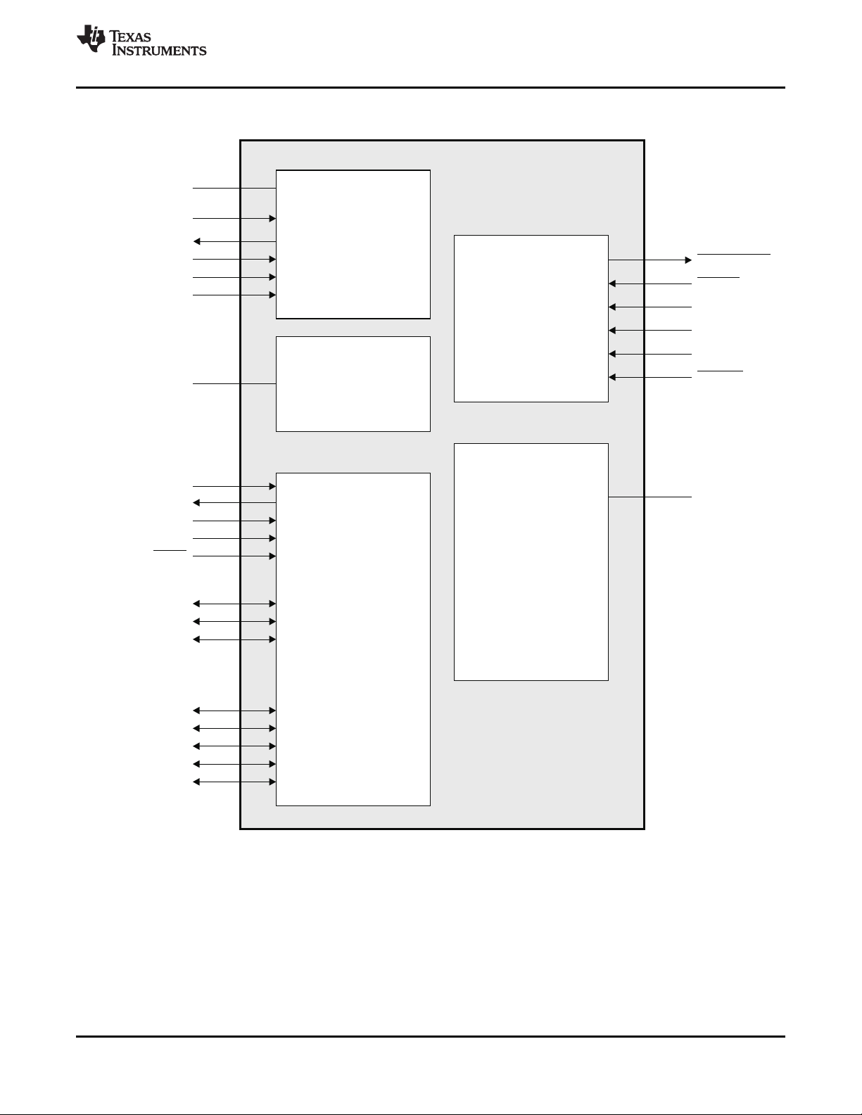
DSP Subsystem 2
C64x+ Megamodule
Power Control
System
L1P Memory Controller (Memory Protect/Bandwidth Mgmt)
Instruction Fetch
EDMA 3.0
A Register File
A31 - A16
A15 - A0
B Register File
B31 - B16
B15 - B0
.L1
.S1
.M1
xx
xx
.D1
C64x+ DSP Core
Interrupt Exception Controller
L2 Memory Controller
(Memory Protect/
Bandwidth Mgmt)
Internal DMA
(DMA)
32K Bytes
L1P SRAM/Cache
Direct-Mapped
32K Bytes Total
L1D SRAM/Cache 2-Way
Set Associative
PLL1 and
PLL1 Controller
Semaphore
Power-Down and Device
Configuration Logic
L3 ROM
Boot Configuration
Sw itc he d C entra l R es ou rce ( SC R)
DDR2 Memory
Controller
PLL2
Serial RapidIO
(2x)
TCP2
VCP2
McBSP0
EMAC
10/100/1000
SGMII
MDIO
Timer [0-5]
I2C
GPIO16
FSYNC
Antenna
Interface
32
DDR2 SDRAM
L1 Data Memory Controller (Memory Protect/Bandwidth Mgmt)
DSP Subsystem 1
DSP Subsystem 0
2
McBSP1
16
.D2
.M2
xx
xx
.S2
.L2
16-/32-bit
Instruction Dispatch
Instruction Decode
Control Registers
SPLOOP Buffer
In-Circuit Emulation
www.ti.com
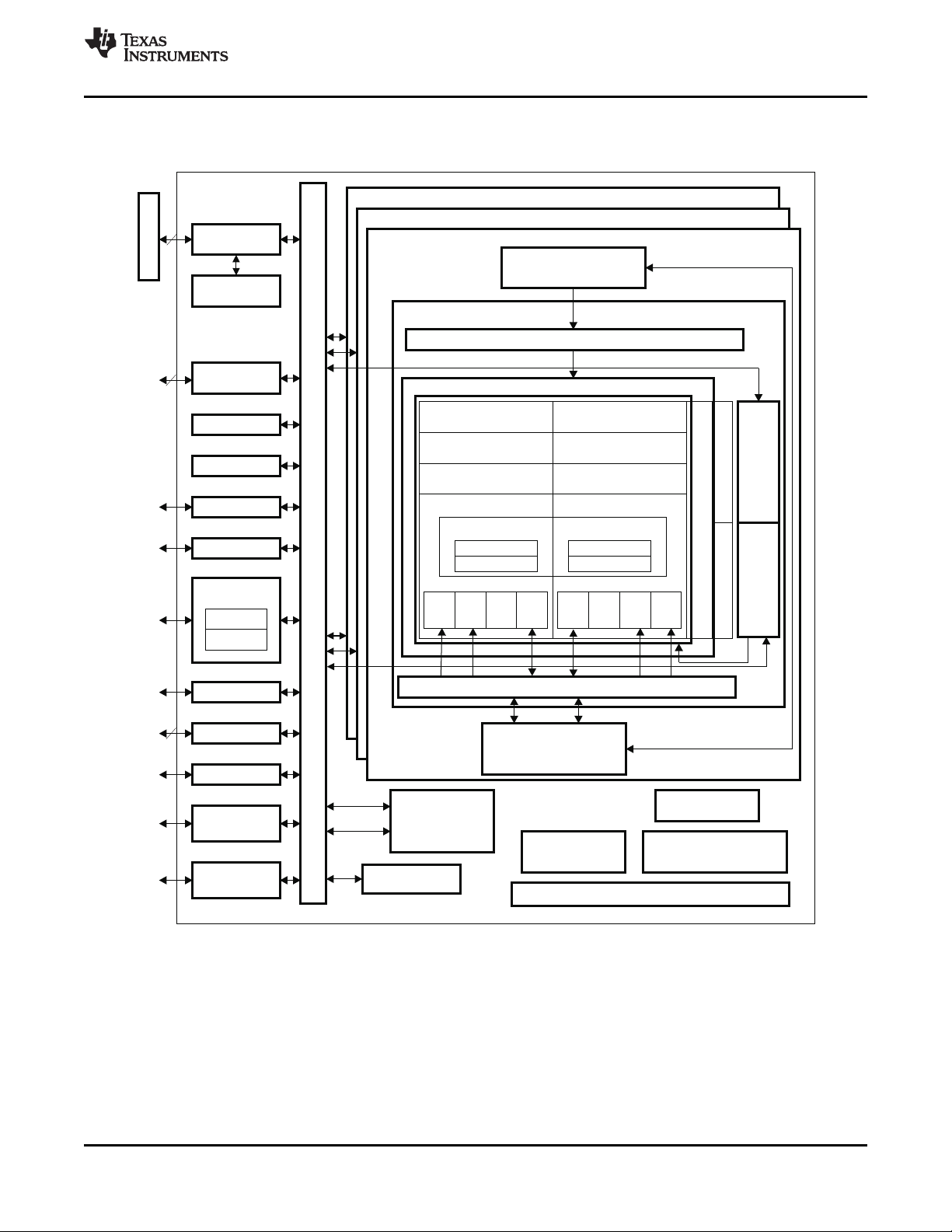
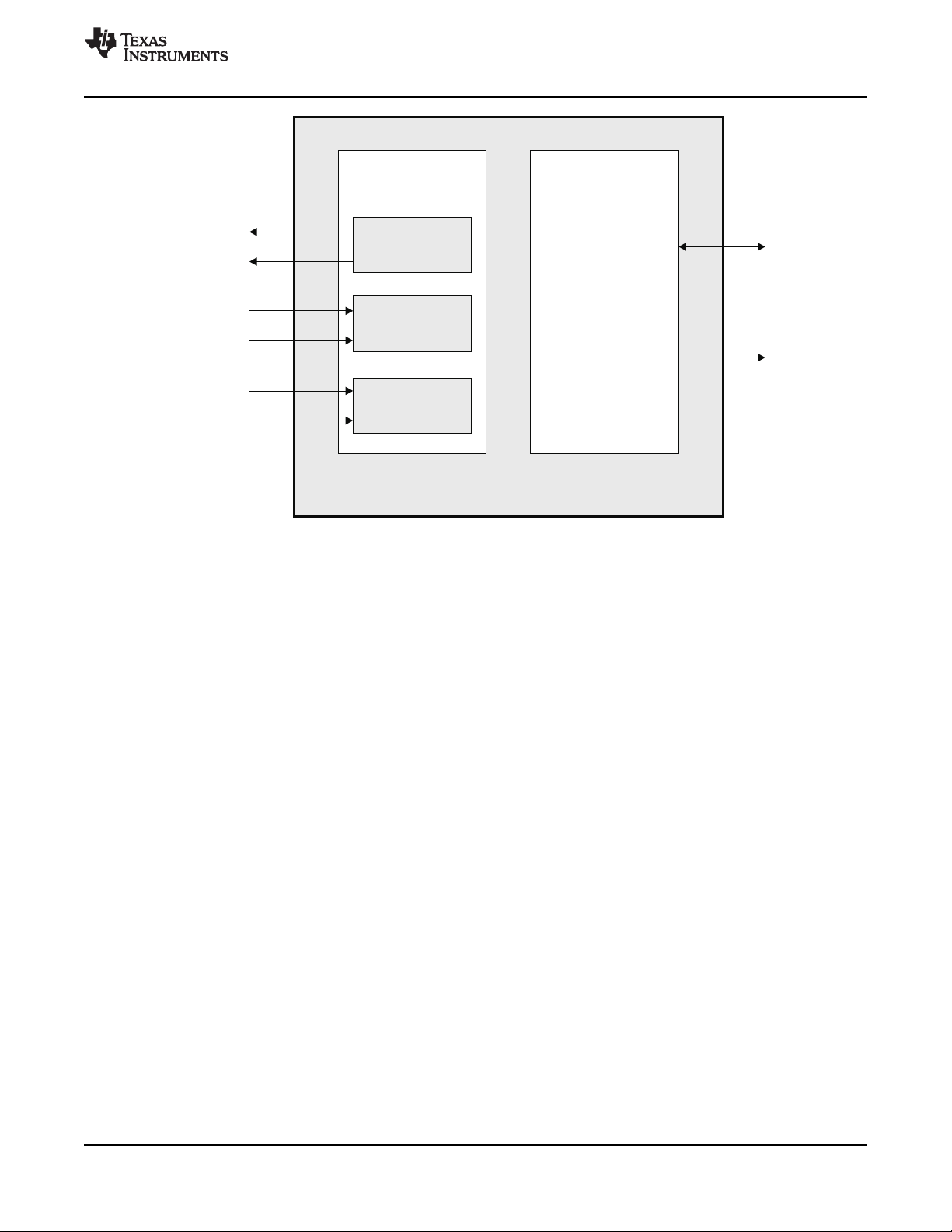
1.3 C6474 Functional Block Diagram
Figure 1-2 shows the functional block diagram of the C6474 device.
TMS320C6474
SPRS552F–OCTOBER 2008–REVISED JULY 2010
Figure 1-2. Functional Block Diagram
Copyright © 2008–2010, Texas Instruments Incorporated Features 5
Submit Documentation Feedback
Product Folder Link(s) :TMS320C6474
Page 6

TMS320C6474
SPRS552F–OCTOBER 2008–REVISED JULY 2010
www.ti.com
1 Features ................................................... 1
1.1 CUN/GUN/ZUN BGA Package (Bottom View) ....... 2
1.2 Description ........................................... 3
1.3 C6474 Functional Block Diagram .................... 5
Revision History .............................................. 7
2 Device Overview ........................................ 8
2.1 Device Characteristics ............................... 8
2.2 CPU (DSP Core) Description ........................ 9
2.3 Memory Map Summary ............................. 12
2.4 Boot Sequence ..................................... 15
2.5 Pin Assignments .................................... 17
2.6 Signal Groups Description .......................... 21
2.7 Terminal Functions ................................. 26
2.8 Development ........................................ 41
3 Device Configuration ................................. 45
3.1 Device Configuration at Device Reset .............. 45
3.2 Peripheral Selection After Device Reset ........... 45
3.3 Device State Control Registers ..................... 46
3.4 Device Status Register Descriptions ............... 47
3.5 Inter-DSP Interrupt Registers (IPCGR0-IPCGR2
and IPCAR0-IPCAR2) .............................. 49
3.6 JTAG ID (JTAGID) Register Description ........... 50
3.7 Debugging Considerations ......................... 50
4 System Interconnect .................................. 51
4.1 Internal Buses, Switch Fabrics, and
Bridges/Gaskets .................................... 51
4.2 Data Switch Fabric Connections ................... 52
4.3 Configuration Switch Fabric ........................ 55
4.4 Priority Allocation ................................... 57
5 C64x+ Megamodule ................................... 58
5.1 Megamodule Diagram .............................. 58
5.2 Memory Architecture ............................... 59
5.3 Memory Protection ................................. 61
5.4 Bandwidth Management ............................ 62
5.5 Power-Down Control ............................... 63
5.6 Megamodule Resets ................................ 63
5.7 Megamodule Revision .............................. 63
5.8 C64X+ Megamodule Register Description(s) ....... 64
6 Device Operating Conditions ....................... 72
6.1 Absolute Maximum Ratings Over Operating Case
Temperature Range (Unless Otherwise Noted) .... 72
6.2 Recommended Operating Conditions .............. 73
6.3 Electrical Characteristics Over Recommended
Ranges of Supply Voltage and Operating Case
Temperature (Unless Otherwise Noted) ............ 74
7 Peripheral Information and Electrical
Specifications .......................................... 75
7.1 Parameter Information .............................. 75
7.2 Recommended Clock and Control Signal Transition
Behavior ............................................ 76
7.3 Power Supplies ..................................... 76
7.4 Peripheral IDs (PIDs) ............................... 79
7.5 Enhanced Direct Memory Access (EDMA3)
Controller ........................................... 80
7.6 Interrupts .......................................... 104
7.7 Reset Controller ................................... 112
7.8 PLL1 and PLL1 Controller ......................... 117
7.9 PLL2 and PLL2 Controller ......................... 130
7.10 DDR2 Memory Controller ......................... 132
7.11 I2C Peripheral ..................................... 135
7.12 Multichannel Buffered Serial Port (McBSP) ....... 140
7.13 Ethernet MAC (EMAC) ............................ 149
7.14 Management Data Input/Output (MDIO) .......... 156
7.15 Timers ............................................. 158
7.16 Enhanced Viterbi-Decoder Coprocessor (VCP2)
..................................................... 167
7.17 Enhanced Turbo Decoder Coprocessor (TCP2)
..................................................... 169
7.18 Serial RapidIO (SRIO) Port ....................... 171
7.19 General Purpose Input/Output (GPIO) ............ 183
7.20 Emulation Features and Capability ............... 184
7.21 Semaphore ........................................ 188
7.22 Antenna Interface Subsystem ..................... 191
7.23 Frame Synchronization ............................ 203
8 Mechanical Data ...................................... 207
8.1 Thermal Data ...................................... 207
8.2 Packaging Information ............................ 207
6 Contents Copyright © 2008–2010, Texas Instruments Incorporated
Submit Documentation Feedback
Product Folder Link(s) :TMS320C6474
Page 7
TMS320C6474
www.ti.com
Revision History
NOTE: Page numbers for previous revisions may differ from page numbers in the current version.
This data manual revision history highlights the technical changes made to the data manual in this
revision.
Scope: Applicable updates to the C64x device family, specifically relating to the TMS320C6474 device,
have been incorporated.
C6474 Revision History
SEE ADDITIONS/MODIFICATIONS/DELETIONS
Section 7.3.1 Power-Supply Sequencing:
Added Footnote (1) to Table 7-1, Timing Requirements for Power Supply Ramping
Modified Figure 7-4, Power-Supply Timing
Section 7.7.2 Warm Reset:
Added last paragraph
SPRS552F–OCTOBER 2008–REVISED JULY 2010
Copyright © 2008–2010, Texas Instruments Incorporated Contents 7
Submit Documentation Feedback
Product Folder Link(s) :TMS320C6474
Page 8
TMS320C6474
SPRS552F–OCTOBER 2008–REVISED JULY 2010
2 Device Overview
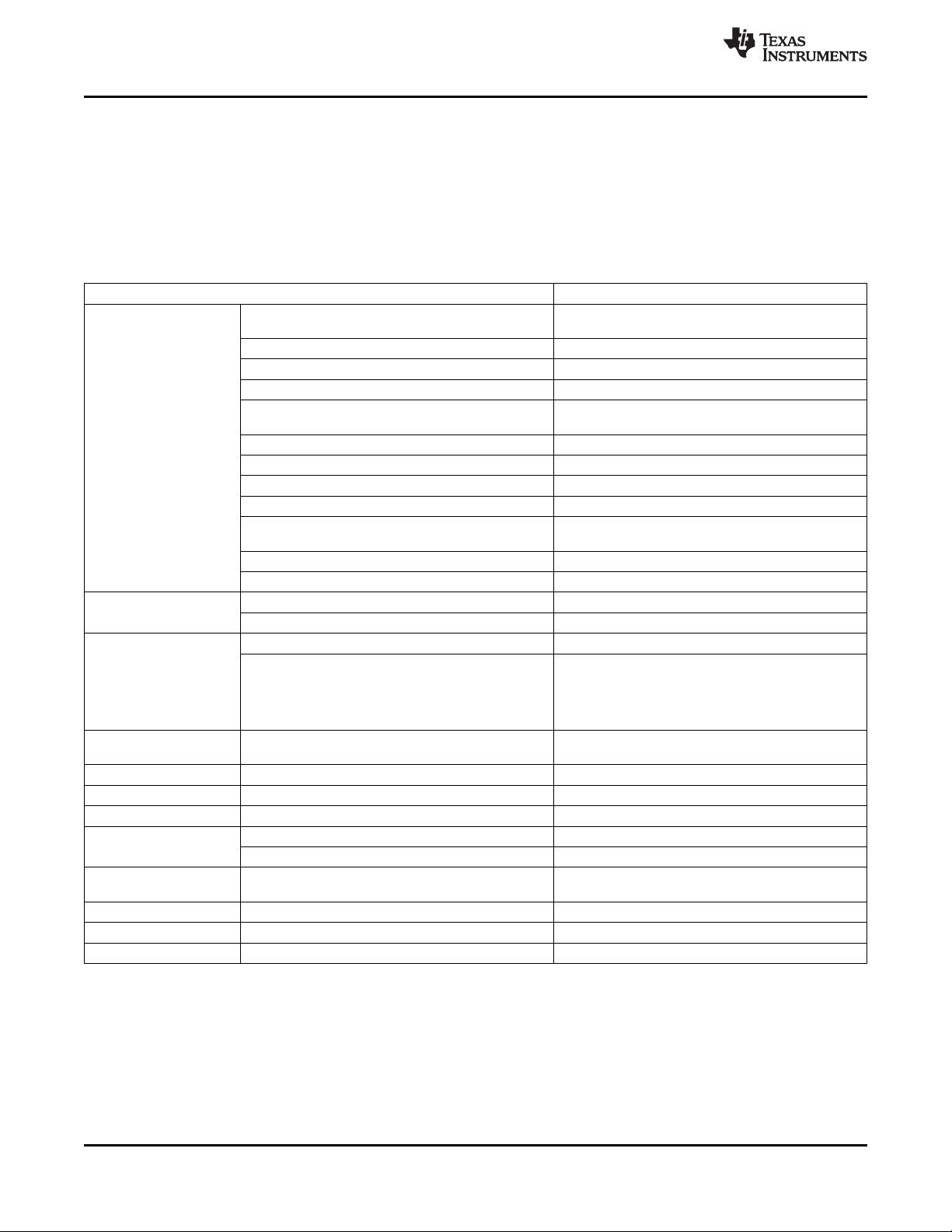
2.1 Device Characteristics
Table 2-1 provides an overview of the C6474 DSP. The tables show significant features of the C6474
device, including the capacity of on-chip RAM, the peripherals, the CPU frequency, and the package type
with pin count.
Table 2-1. Characteristics of the C6474 Processor
HARDWARE FEATURES C6474
Peripherals DDR2 Memory Controller (32-bit bus width) [1.8 V I/O]
Not all peripherals pins (clock memory = DDRREFCLK(N|P)
are available at the same
time.
(For more detail, see
Section 3, Device
Configuration)
Decoder Coprocessors VCP2 (clock source = CPU/3 clock frequency) 1
On-Chip Memory Size (Bytes) 3200 KB
CPU Megamodule Revision ID Register
Revision ID (MM_REVID. [15:0]) 0x0181 2000)
JTAG Device_ID JTAG Register (address location: 0x0288 0814) For details, see Section 3.6
Frequency MHz 850 - 1200 (850 MHz to 1.2 GHz)
Cycle Time ns 1.18 ns - 0.83 ns (850 MHz to 1.2 GHz CPU)
Voltage Core (V) 0.9-V to 1.2-V SmartReflex
PLL1 and PLL1 Controller CLKIN1 Frequency Multiplier
Options
PLL2 DDR Clock X10
BGA Package 23 X 23 mm 561-Pin Flip-Chip with BGA CUN/GUN/ZUN
Process Technology mm 0.065 mm
(1) A heatsink and implementation of the SmartReflex solution is required for proper device operation. For more details on SmartReflex, see
Section 7.3.4.
EDMA3 (64 independent channels [CPU/3 clock rate] 1
High-speed 1x Serial RapidIO Port (2 lanes) 1
I2C 1
McBSPs
(internal or external clock source up to 100 Mbps)
1000 Ethernet MAC (EMAC) 1
Management Data Input/Output (MDIO) 1
Antenna Interface (AIF) 1
Frame Synchronization (FSYNC) 1
64-bit Timers (Configurable)
(internal clock source CPU/6 clock frequency)
SYSCLKOUT 1
General Purpose Input/Output Port (GPIO) 16
TCP2 (clock source = CPU/3 clock frequency) 1
Organization 32KB L1P Program Cache (SRAM/Cache)
32KB L1D Data Cache (SRAM/Cache)
3072KB Total L2 Unified Memory SRAM/Cache
I/O (V) 1.8 V, 1.1 V
6 64-bit or 12 32-bit
32KB Data Memory Controller
Bypass (x1), (x4 to x32)
1
2
64KB L3 ROM
0x0
(1)
www.ti.com
1.1 V
8 Device Overview Copyright © 2008–2010, Texas Instruments Incorporated
Submit Documentation Feedback
Product Folder Link(s) :TMS320C6474
Page 9

TMS320C6474
www.ti.com
Table 2-1. Characteristics of the C6474 Processor (continued)
HARDWARE FEATURES C6474
Product Status
Device Part Numbers (For more details on C64x+ DSP part numbering, see
(1) PRODUCTION DATA information is current as of publication date. Products conform to specifications per the terms of Texas
Instruments standard warranty. Production processing does not necessarily include testing of all parameters. Note: Advance Information
is presented in this document for the C6474 1.2-GHz extended temperature device.
(1)
Product Preview (PP), Advance Information (AI), or
Production Data (PD)
Figure 2-11)
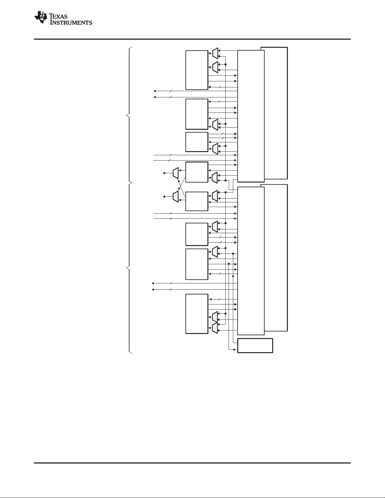
2.2 CPU (DSP Core) Description
The C64x+ central processing unit (CPU) consists of eight functional units, two register files, and two data
paths as shown in Figure 2-1. The two general-purpose register files (A and B) each contain 32 (thirty-two)
32-bit registers for a total of 64 registers. The general-purpose registers can be used for data or can be
data address pointers. The data types supported include packed 8-bit data, 32-bit data, 40-bit data, and
64-bit data. Values larger than 32 bits, such as 40-bit-long or 64-bit-long values are stored in register
pairs, with the 32 LSBs of data placed in an even register and the remaining 8 or 32 MSBs in the next
upper register (which is always an odd-numbered register).
The eight functional units (.M1, .L1, .D1, .S1, .M2, .L2, .D2, and .S2) are each capable of executing one
instruction every clock cycle. The .M functional units perform all multiply operations. The .S and .L units
perform a general set of arithmetic, logical, and branch functions. The .D units primarily load data from
memory to the register file and store results from the register file into memory.
SPRS552F–OCTOBER 2008–REVISED JULY 2010
PD
TMS320C6474CUN/GUN/ZUN
The C64x+ CPU extends the performance of the C64x core through enhancements and new features.
Each C64x+ .M unit can perform one of the following each clock cycle: one 32 x 32 bit multiply, two 16 x
16 bit multiplies, two 16 x 32 bit multiplies, four 8 x 8 bit multiplies, four 8 x 8 multiplies with add
operations and four 16 x 16 multiplies with add/subtract capabilities (including a complex multiply). There
is also support for Galois filed multiplication for 8-bit and 32-bit data. Many communications algorithms
such FFTs and modems require complex multiplication. The complex multiply (CMPY) instruction takes
four 16-bit inputs and produces a 32-bit real and a 32-bit imaginary output. There are also complex
multiplies with rounding capability that produces one 32-bit packed output that contain 16-bit real and
16-bit imaginary values. The 32 x 32 bit multiply instructions provide the extended precision necessary for
audio and other high-precision algorithms on a variety of signed and unsigned 32-bit data types.
The .L or arithmetic logic unit now incorporates the ability to do parallel add/subtract operations on a pair
of common inputs. Versions of this instruction exist to work on 32-bit data or on pairs of 16-bit data
performing dual 16-bit add and subtracts in parallel. There are also saturated forms of these instructions.
The C64x+ core enhances the .S unit in several ways. In the C64x core, dual 16-bit MIN2 and MAX2
comparisons were only available on the .L units. On the C64X+ core, they are also available on the .S unit
which increases the performance of algorithms that do searching and sorting. Finally, to increase data
packing and unpacking throughput, the .S unit allows sustained high performance for the quad 8-bit/16-bit
and dual 16-bit instructions. Unpack instructions prepare 8-bit data for parallel 16-bit operations. Pack
instructions return parallel results to output precision including saturation support.
Other new features include:
• SPLOOP - a small instruction buffer in the CPU that aids in creation of software pipelining loops where
multiple iterations of a loop are executed in parallel. The SPLOOP buffer reduces the code size
associated with software pipelining. Furthermore, loops in the SPLOOP buffer are fully interruptible.
• Compact Instructions - The native instruction size of the C6000 devices is 32 bits. Many common
instructions such as MPY, AND, OR, ADD, and SUB can be expressed as 16 bits if the C64x+
compiler can restrict the code to use certain registers in the register file. This compression is
performed by the code generation tools.
Copyright © 2008–2010, Texas Instruments Incorporated Device Overview 9
Submit Documentation Feedback
Product Folder Link(s) :TMS320C6474
Page 10

TMS320C6474
SPRS552F–OCTOBER 2008–REVISED JULY 2010
• Instruction Set Enhancements - As noted above, there are new instructions such as 32-bit
multiplications, complex multiplications, packing, sorting, bit manipulation, and 32-bit Galois field
multiplication.
• Exception Handling - Intended to aid the programmer in isolating bugs. The C64x+ CPU is able to
detect and respond to exceptions, both from internally detected sources (such as illegal op-codes) and
from system events (such as watchdog time expiration).
• Privilege - Defines user and supervisor modes of operation, allowing the operating system to give a
basic level of protection to sensitive resources. Local memory is divided into multiple pages, each with
read, write, and execute permissions.
• Time-Stamp Counter - Primarily targeted for real-time operating system (RTOS) robustness, a
free-running time-stamp counter is implemented in the CPU that is not sensitive to system stalls.
For more details on the C64x+ CPU and its enhancements over the C64x architecture, see the following
documents:
• TMS320C64x/C64x+ DSP CPU and Instruction Set Reference Guide (literature number SPRU732)
• TMS320C64x+ DSP Cache User's Guide (literature number SPRU862)
• TMS320C64x+ Megamodule Reference Guide (literature number SPRU871)
• TMS320C64X to TMS320C64x+ CPU Migration Guide (literature number SPRAA84)
www.ti.com
10 Device Overview Copyright © 2008–2010, Texas Instruments Incorporated
Submit Documentation Feedback
Product Folder Link(s) :TMS320C6474
Page 11
src2
src2
.D1
.M1
.S1
.L1
longsrc
odddst
src2
src1
src1
src1
src1
evendst
evendst
odddst
dst1
dst
src2
src2
src2
longsrc
DA1
ST1b
LD1b
LD1a
ST1a
Datapath A
Odd
register
fileA
(A1, A3,
A5...A31)
Odd
register
fileB
(B1,B3,
B5...B31)
.D2
src1
dst
src2
DA2
LD2a
LD2b
src2
.M2
src1
dst1
.S2
src1
evendst
longsrc
odddst
ST2a
ST2b
longsrc
.L2
evendst
odddst
src1
Data pathB
Control Register
32MSB
32LSB
dst2
(A)
32MSB
32LSB
2x
1x
32LSB
32MSB
32LSB
32MSB
dst2
(B)
(B)
(A)
8
8
8
8
32
32
32
32
(C)
(C)
Even
register
file A
(A0, A2,
A4...A30)
Even
register
fileB
(B0,B2,
B4...B30)
(D)
(D)
(D)
(D)
www.ti.com
TMS320C6474
SPRS552F–OCTOBER 2008–REVISED JULY 2010
A. On .M unit, dst2 is 32 MB.
B. On .M unit, dst1 is 32 LSB.
C. On 64x+ CPU .M unit, src2 is 32 bits; on C64x+ CPU .M unit, src2 is 64 bits.
D. On .L and .S units, odd dst connects to odd register files and even dst connects to even register files.
Copyright © 2008–2010, Texas Instruments Incorporated Device Overview 11
Figure 2-1. TMS320C64x+TM CPU (DSP Core) Data Path
Submit Documentation Feedback
Product Folder Link(s) :TMS320C6474
Page 12
TMS320C6474
SPRS552F–OCTOBER 2008–REVISED JULY 2010
2.3 Memory Map Summary
Table 2-2 shows the memory map address of the C6474 device. For more information about the registers
in these address ranges, click on the links in the table. The external memory configuration register
address ranges in the C6474 device begin at the hex address location 0x7000 for DDR2 Memory
Controller.
Table 2-2. Memory Map Summary
HEX ADDRESS RANGE MEMORY BLOCK DESCRIPTION
START END C64x+ MEGAMODULE CORE0 C64x+ MEGAMODULE CORE1 C64x+ MEGAMODULE CORE 2
0000 0000 007F FFFF 8M Reserved
0080 0000 0087 FFFF 512K
0088 0000 008F FFFF 512K
009 00000 0097 FFFF 512K Reserved
0098 0000 009F FFFF 512K Reserved
00A0 0000 00DF FFFF 4M Reserved
00E0 0000 00E0 7FFF 32K L1PSRAM
00E0 8000 00EF FFFF 1M - 32K Reserved
00F0 0000 00F0 7FFF 32K L1D SRAM
00F0 8000 00FF FFFF 1M - 32K Reserved
0100 0000 01BF FFFF 4M C64x+ Megamodule Registers
01C0 0000 027F FFFF 12.5M Reserved
0280 0000 0280 03FF 1K Frame Synchronization (FSYNC)
0280 0400 0287 FFFF 511K Reserved
0288 0000 0288 00FF 256 Chip Interrupt Controller0 (CIC0)
0288 0100 0288 01FF 256 Chip Interrupt Controller1 (CIC1)
0288 0200 0288 02FF 256 Chip Interrupt Controller2 (CIC2)
0288 0300 0288 03FF 256 Chip Interrupt Controller3 (CIC3)
0288 0400 0288 0403 4 DSP Trace Formatter1 (DTF1)
0288 0404 0288 0407 4 DSP Trace Formatter2 (DTF2)
0288 0408 0288 040B 4 DSP Trace Formatter3 (DTF3)
0288 040C 0288 07FF 1K- 6 Reserved
0288 0800 0288 0BFF 1K CFGC
0288 0900 0288 0903 4B IPCGR0
0288 0904 0288 0907 4B IPCGR1
0288 0908 0288 090B 4B IPCGR2
0288 090C 0288 093F 52B Reserved
0288 0940 0288 0943 4B IPCAR0
0288 0944 0288 0947 4B IPCAR1
0288 0948 0288 094B 4B IPCAR2
0288 0C00 028B FFFF 253K Reserved
028C 0000 028C 00FF 256 McBSP0
028C 0100 028C FFFF 64K - 256 Reserved
028D 0000 208D 00FF 256 McBSP1
028D 0100 028D FFFF 64K - 256 Reserved
028E 0000 028F FFFF 128K Reserved
0290 0000 0290003F 64 Timer Pin Manager (TPMGR)
0290 0040 0290 FFFF 64K - 64 Reserved
0291 0000 0291003F 64 Timer0
0291 0040 0291 FFFF 64K - 64 Reserved
0292 0000 0292003F 64 Timer1
0292 0040 0292 FFFF 64K - 64 Reserved
0293 0000 0293003F 64 Timer2
0293 0040 0293 FFFF 64K - 64 Reserved
0294 0000 0294003F 64 Timer3
0294 0040 0294 FFFF 64K - 64 Reserved
SIZE
Internal RAM
L2 SRAM
Control Registers onCFG SCR
www.ti.com
12 Device Overview Copyright © 2008–2010, Texas Instruments Incorporated
Submit Documentation Feedback
Product Folder Link(s) :TMS320C6474
Page 13
www.ti.com
TMS320C6474
SPRS552F–OCTOBER 2008–REVISED JULY 2010
HEX ADDRESS RANGE MEMORY BLOCK DESCRIPTION
START END C64x+ MEGAMODULE CORE0 C64x+ MEGAMODULE CORE1 C64x+ MEGAMODULE CORE 2
0295 0000 0295003F 64 Timer4
0295 0040 0295 FFFF 64K - 64 Reserved
0296 0000 0296003F 64 Timer5
0296 0040 0296 FFFF 256K - 64 Reserved
029A 0000 029A 01FF 512 PLLController 1 (Main)
029A 0200 029B FFFF 128K - 512 Reserved
029C 0000 029C 01FF 512 Reserved
029C 0200 029C 02FF 256K - 512 Reserved
02A0 0000 02A0 7FFF 32K EDMA3 Channel Controller(TPCC)
02A0 8000 02A1 FFFF 96K Reserved
02A2 0000 02A2 7FFF 32K EDMA3 Transfer Controller0 (TPTC0)
02A2 8000 02A2 FFFF 32K EDMA3 Transfer Controller 1 (TPTC1)
02A3 0000 02A3 7FFF 32K EDMA3 Transfer Controller2 (TPTC2)
02A3 8000 02A3 FFFF 32K EDMA3 Transfer Controller 3 (TPTC3)
02A4 0000 02A4 7FFF 32K EDMA3 Transfer Controller4 (TPTC4)
02A4 8000 02A4 FFFF 32K EDMA3 Transfer Controller 5 (TPTC5)
02A5 0000 02A7 FFFF 192K Reserved
02A8 0000 02A8 00FF 256 Reserved
02A8 0100 02AB FFFF 256K -256 Reserved
02AC 0000 02AC 0FFF 4K Power/Sleep Controller (PSC)
02AC 1000 02AC 3FFF 12K Reserved
02AC 4000 02AC 40FF 256 Reserved
02AC 4100 02AC FFFF 48K - 256 Reserved
02AD 0000 02AD 7FFF 32K Embedded Trace Buffer0 (ETB0)
02AD 8000 02AD FFFF 32K Embedded TraceBuffer 1 (ETB1)
02AE 0000 02AE 7FFF 32K Embedded Trace Buffer 2 (ETB2)
02AE 8000 02AF FFFF 96K Reserved
02B0 0000 02B0 00FF 256 GPIO
02B0 0100 02B0 1FFF 8K - 256 Reserved
02B0 2000 02B0 23FF 1K Reserved
02B0 2400 02B0 3FFF 7K Reserved
02B0 4000 02B0 407F 128 I2C Data andControl
02B0 4080 02B3 FFFF 256K - 128 Reserved
02B4 0000 02B4 07FF 2K Semaphore
02B4 0800 02B7 FFFF 254K Reserved
02B8 0000 02B8 00FF 256 VCP2 Control
02B8 0100 02B8 FFFF 128K - 256 Reserved
02BA 0000 02BA 00FF 256 TCP2 Control
02BA 0100 02BB FFFF 128K - 256 Reserved
02BC 0000 02BF FFFF 256K Antenna Interface Control
02C0 0000 02C0 03FF 1K Reserved
02C0 0400 02C3 FFFF 255K Reserved
02C4 0000 02C4 00FF 256 SMGII Control
02C4 0100 02C7 FFFF 256K - 256 Reserved
02C8 0000 02C8 07FF 2K EMAC Control
02C8 0800 02C8 0FFF 2K Reserved
02C8 1000 02C8 10FF 256 EMAC Interrupt Controller
02C8 1100 02C8 17FF 2K - 256 Reserved
02C8 1800 02C8 18FF 256 MDIO
02C8 1900 02C8 FFFF 2K- 256 Reserved
02C8 2000 02C8 3FFF 8K EMAC Descriptor Memory
02C8 4000 02CF FFFF 496K Reserved
02D0 0000 02D2 0FFF 132K RapidIO
02D2 1000 02D3 FFFF 124K Reserved
02D4 0000 02D7 FFFF 256K Reserved
02D8 0000 02DB FFFF 256K Reserved
SIZE
Copyright © 2008–2010, Texas Instruments Incorporated Device Overview 13
Submit Documentation Feedback
Product Folder Link(s) :TMS320C6474
Page 14
TMS320C6474
SPRS552F–OCTOBER 2008–REVISED JULY 2010
www.ti.com
HEX ADDRESS RANGE MEMORY BLOCK DESCRIPTION
START END C64x+ MEGAMODULE CORE0 C64x+ MEGAMODULE CORE1 C64x+ MEGAMODULE CORE 2
02DC 0000 02DF FFFF 256K Reserved
02E0 0000 02E0 3FFF 16K RapidIO Descriptor Memory
02E0 4000 02EF FFFF 1M - 16K Reserved
02F0 0000 02F0 FFFF 64K Reserved
02F1 0000 02F1 FFFF 64K Reserved
02F2 0000 02F3 FFFF 128K Reserved
02F4 0000 02F5 FFFF 128K Reserved
02F6 0000 02FF FFFF 576K Reserved
0300 0000 03FF FFFF 16M Reserved
0400 0000 0FFF FFFF 192M Reserved
1000 0000 107F FFFF 8M Reserved
1080 0000 1087 FFFF 512K
1088 0000 108F FFFF 512K
1090 0000 1097 FFFF 512K Reserved
1098 0000 109F FFFF 512K Reserved
10A0 0000 10DF FFFF 4M Reserved
10E0 0000 10E0 7FFF 32K C64x+ Megamodule Core0 L1P SRAM
10E0 8000 10EF FFFF 1M - 32K Reserved
10F0 0000 10F0 7FFF 32K C64x+ Megamodule Core 0 L1D SRAM
10F0 8000 10FF FFFF 1M - 32K Reserved
1100 0000 117F FFFF 8M Reserved
1180 0000 1187 FFFF 512K
1188 0000 118F FFFF 512K
1190 0000 1197 FFFF 512K Reserved
1198 0000 119F FFFF 512K Reserved
11A0 0000 11DF FFFF 4M Reserved
11E0 0000 11E0 7FFF 32K C64x+ Megamodule Core1 L1P SRAM
11E0 8000 11EF FFFF 1M - 32K Reserved
11F0 0000 11F0 7FFF 32K C64x+ Megamodule Core 1 L1D SRAM
11F0 8000 11FF FFFF 1M - 32K Reserved
1200 0000 127F FFFF 8M Reserved
1280 0000 1287 FFFF 512K
1288 0000 128F FFFF 512K
1290 0000 1297 FFFF 512K Reserved
1298 0000 129F FFFF 512K Reserved
12A0 0000 12DF FFFF 4M Reserved
12E0 0000 12E0 7FFF 32K C64x+ Megamodule Core2 L1P SRAM
12E0 8000 12EF FFFF 1M - 32K Reserved
12F0 0000 12F0 7FFF 32K C64x+ Megamodule Core 2 L1D SRAM
12F0 8000 12FF FFFF 1M - 32K Reserved
1300 0000 1FFF FFFF 208M Reserved
2000 0000 2FFF FFFF 256M Reserved
3000 0000 3000 00FF 256 McBSP0 Data
3000 0100 33FF FFFF 64M - 256 Reserved
3400 0000 3400 00FF 256 McBSP1 Data
3400 0100 3BFF FFFF 128M - 256 Reserved
3C00 0000 3C00 FFFF 64K L3 ROM
3C01 0000 3FFF FFFF 64M - 64K Reserved
4000 0000 4FFF FFFF 256M Reserved
5000 0000 500F FFFF 1M TCP2 Data
5010 0000 57FF FFFF 127M Reserved
5800 0000 5800 FFFF 64K VCP2 Data
5801 0000 5FFF FFFF 128M 64K Reserved
SIZE
Reserved
Global Ram
C64x+ Megamodule Core0 L2 RAM
C64x+ Megamodule Core1 L2 SRAM
C64x+ Megamodule Core2 L2 SRAM
Data Space onEDMA SCR
14 Device Overview Copyright © 2008–2010, Texas Instruments Incorporated
Submit Documentation Feedback
Product Folder Link(s) :TMS320C6474
Page 15
www.ti.com
TMS320C6474
SPRS552F–OCTOBER 2008–REVISED JULY 2010
HEX ADDRESS RANGE MEMORY BLOCK DESCRIPTION
START END C64x+ MEGAMODULE CORE0 C64x+ MEGAMODULE CORE1 C64x+ MEGAMODULE CORE 2
6000 0000 603F FFFF 4M Reserved
6040 0000 6FFF FFFF 252M Reserved
7000 0000 7000 00FF 256 DDR2 EMIF Configuration
7000 0100 7FFF FFFF 256M - 256 Reserved
8000 0000 9FFF FFFF 512M DDR2EMIF Data
A000 0000 AFFF FFFF 256M AIF Data
B000 0000 BFFF FFFF 256m Reserved
C000 0000 CFFF FFFF 256m Reserved
D000 0000 DFFF FFFF 256m Reserved
E000 0000 EFFF FFFF 256m Reserved
F000 0000 FFFF FFFF 256m Reserved
SIZE
2.4 Boot Sequence
The boot sequence is a process by which the DSP's internal memory is loaded with program and data
sections. The DSP's internal registers are programmed with predetermined values. The boot sequence is
started automatically after each power-on reset, warm reset, and system reset. A local reset to an
individual C64x+ Megamodule should not affect the state of the hardware boot controller on the device.
For more details on the initiators of the resets, see Section 7.7, Reset Controller.
The C6474 device supports several boot processes begins execution at the ROM base address, which
contains the bootloader code necessary to support various device boot modes. The boot processes are
software driven; using the BOOTMODE[3:0] device configuration inputs to determine the software
configuration that must be completed.
2.4.1 Boot Modes Supported
The device supports several boot processes, which leverage the internal boot ROM. Most boot processes
are software driven, using the BOOTMODE[3:0] device configuration inputs to determine the software
configuration that must be completed. From a hardware perspective, there are three possible boot modes:
• No Boot (BOOTMODE[3:0] = 0000b)
With no boot, the CPU executes directly from the internal L2 RAM located at address 0x80 0000.
Note: Device operations are undefined if invalid code is located at address 0x80 0000. This boot mode
is a hardware boot mode.
• Public ROM Boot
The C64x+ Megamodule Core 0 is released from reset and begins executing from the L3 ROM base
address. C64x+ Megamodule Core 0 is responsible for performing the boot process (e.g., from I2C
ROM, Ethernet, or RapidIO), after which C64x+ Megamodule Core 0 brings the other C64x+
megamodule cores out of reset by setting to 1 the EVTPULSE4 bit (bit 4) of the C64x+ Megamodule
Core 0's EVTASRT register. This process is valid only once: writing 1, then writing 1 again will not
bring Core 1 and 2 out of reset again. Then, the C64x+ Megamodule Core 0 begins execution from the
entry address defined in the boot table. The C64x+ Megamodule Core 1 and 2 begin execution from
their L2 RAMs' base address.
The boot process performed by C64x+ Megamodule Core 0 in public ROM boot is determined by the
BOOTMODE[3:0] value in the DEVSTAT register. C64x+ Megamodule Core 0 reads this value, and then
executes the associated boot process in software.
Copyright © 2008–2010, Texas Instruments Incorporated Device Overview 15
Submit Documentation Feedback
Product Folder Link(s) :TMS320C6474
Page 16
TMS320C6474
SPRS552F–OCTOBER 2008–REVISED JULY 2010
Table 2-3. C6474 Supported Boot Modes
MODE NAME BOOTMODE[3:0] DESCRIPTION
No Boot 0000b No Boot (BOOTMODE[3:0] = 0000b)
I2C Master Boot A 0001b Slave I2C address is 0x50. C64x+ Megamodule Core 0 configures I2C, acts as a
I2C Master Boot B 0010b Similar to I2C boot A except the slave I2C address is 0x51.
I2C Slave Boot 0011 The C64x+ Megamodule Core 0 configures I2C and acts as a slave and will accept
EMAC Master Boot 0100b TI Ethernet Boot, C64x+ Megamodule Core 0 configures EMAC0 and EDMA, if
EMAC Slave Boot 0101b
EMAC Forced-Mode Boot 0110b
Reserved 0111b Reserved
Serial RapidIO Boot (Config 0) 1000b The C64x+ Megamodule Core 0 configures the SRIO and an external host loads the
Serial RapidIO Boot (Config 1) 1001b
Serial RapidIO Boot (Config 2) 1010b
Serial RapidIO Boot (Config 3) 1011b
master to the I2C bus and copies data from an I2C EEPROM or a device acting as an
I2C slave to the DSP using a predefined boot table format. The destination address
and length are contained within the boot table. After boot table copy is complete, the
C64x+ Megamodule Core 0 brings the other C64x+ Megamodule Cores out of reset
by setting to 1 the EVTPULSE4 bit (bit 4) of the C64x+ Megamodule Core EVTASRT
register.
data and code section packets through the I2C interface. It is required that an I2C
master in present in the system.
required, and brings the code image into the internal on-chip memory via the protocol
defined by the boot method (EMAC bootloader). After initializing the on-chip memory
to the known state, C64x+ Megamodule Core 0 brings the other C64x+ Megamodule
Cores out of reset.
application via SRIO peripheral, using directIO protocol. A doorbell interrupt is used to
indicate that the code has been loaded. For more details on the Serial RapidIO
configurations, see Table 2-4.
www.ti.com
C64x+ Megamodule Core 0 configures Serial RapidIO and EDMA, if required, and brings the code image
into the internal on-chip memory via the protocol defined by the boot method (SRIO bootloader) and then
C64x+ Megamodule Core 0 brings the other C64x+ Megamodule Cores out of reset. Note that SRIO boot
modes are only supported on port 0.
Table 2-4. Serial RapidIO (SRIO) Supported Boot Modes
SRIO BOOT MODE SERDES CLOCK LINK RATE BOOTMODE[3:0]
Bootmode 8 - Config 0 125 MHz 1.25 Gbps 1000b
Bootmode 9 - Config 1 125 MHz 3.125 Gbps 1001b
Bootmode 10 - Config 2 156.25 MHz 1.25 Gbps 1010b
Bootmode 11 - Config 3 156.25 MHz 3.125 Gbps 1011b
All the other BOOTMODE[3:0] modes are reserved.
2.4.2 Second-Level Bootloaders
Any of the boot modes can be used to download a second-level bootloader. A second-level bootloader
allows for any level of customization to current boot methods as well as the definition of a completely
customized boot.
16 Device Overview Copyright © 2008–2010, Texas Instruments Incorporated
Submit Documentation Feedback
Product Folder Link(s) :TMS320C6474
Page 17
AE
AD
AC
AB
AA
Y
W
V
U
T
R
13121110987654321
131211109876
5
4321
AF
AG
14
14
AE
AD
AC
AB
AA
Y
W
V
U
T
R
AF
AG
RSV04
AIF_V
DDT11
V
SS
AIFTXN4
AIFTXP4
ALTCORE
CLKN
V
SS
AIFRXN5
AIFRXP5
V
SS
V
SS
AIF_V
DDT11
AIF_V
DDA11
V
SS
AIF_V
DDT11
SYSCLKN
V
SS
V
SS
AIFRXP4
AIFRXN4
FRAME
BURSTN
V
SS
AIFTXP5
AIFTXN5
RSV02
DV
DD18
V
SS
V
SS
V
SS
V
SS
CV
DDMON
DV
DD18MON
ALTFSYNC
CLK
CORECLK
SEL
ALTFSYNC
PULSE
RSV06
SYSCLK
OUT
FSYNC
CLKP
V
SS
DV
DD18
DV
DD18
AV
DD118
V
SS
ALTCORE
CLKP
RSV07 SYSCLKP
V
SS
V
SS
V
SS
RESETSTAT
DV
DD18
V
SS
V
SS
V
SS
RSV23
POR
V
SS
V
SS
TRT
SMFRAME
CLK
XWRST
DV
DD18
V
SS
GP15 TRTCLK
DV
DD18
GP12 GP11
V
SS
GP13
V
SS
V
SS
GP14
GP10
DV
DD18
V
SS
V
SS
GP08
GP07DV
DD18
CV
DD
V
SS
CV
DD
V
SS
CV
DD
V
SS
FSYNC
CLKN
FRAME
BURSTP
V
SS
DV
DD18
TMS
GP02
TRST
TDO
TCK
DV
DD18
GP05
GP06
TDI V
SS
V
SS
CV
DD
V
SS
CV
DD
V
SS
CV
DD
EMU10
DV
DD18
EMU15
V
SS
GP03
GP01
DV
DD18
DV
DD18
GP04
EMU00
V
SS
EMU01 EMU07
EMU11
GP00
GP09
CV
DD
V
SS
CV
DD
V
SS
CV
DD
V
SS
V
SS
CV
DD
V
SS
CV
DD
V
SS
CV
DD
CV
DD
V
SS
CV
DD
V
SS
CV
DD
V
SS
www.ti.com
SPRS552F–OCTOBER 2008–REVISED JULY 2010
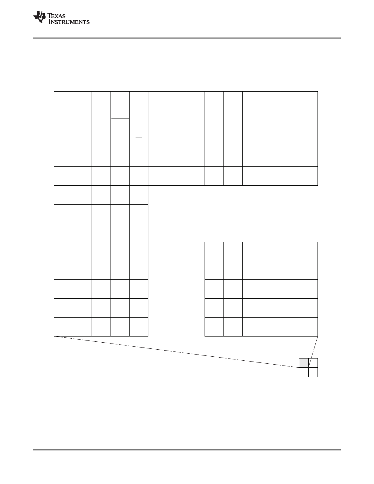
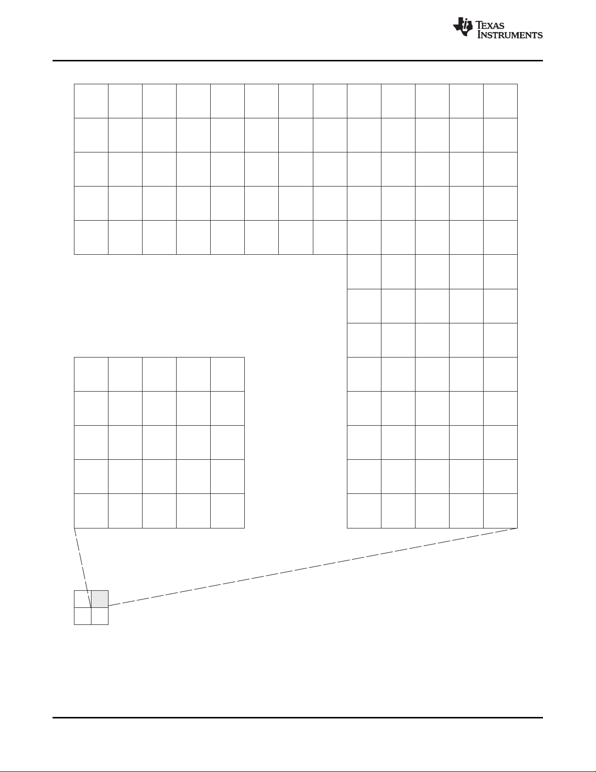
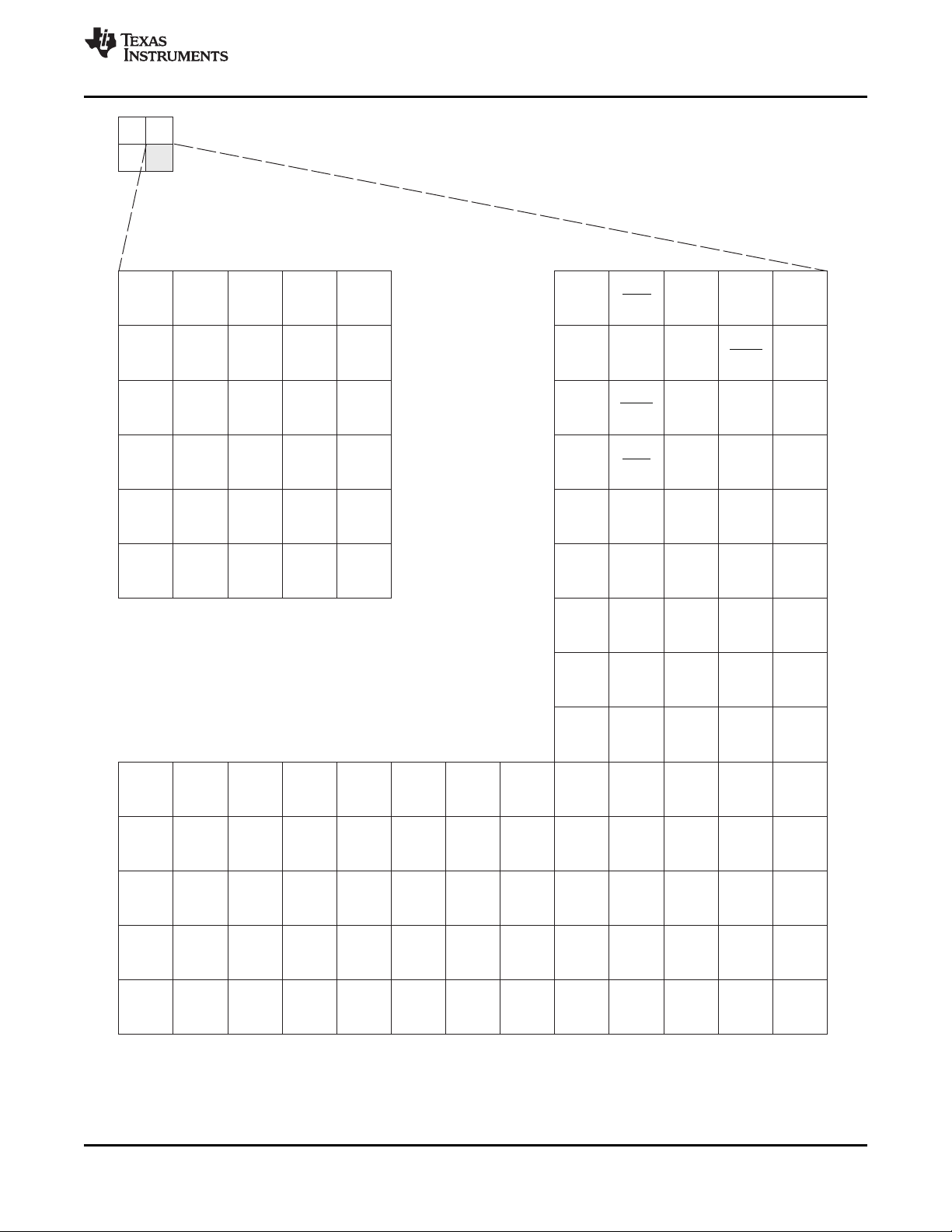
2.5 Pin Assignments
2.5.1 Pin Map
Figure 2-2 through Figure 2-5 show the C6474 pin assignments in four quadrants (A, B, C, and D).
TMS320C6474
Figure 2-2. C6474 Pin Map (Bottom View) [Quadrant A]
Copyright © 2008–2010, Texas Instruments Incorporated Device Overview 17
Submit Documentation Feedback
Product Folder Link(s) :TMS320C6474
Page 18
AE
AD
AC
AB
AA
Y
W
V
U
T
R
26252423222120
19
18171615
26
2524
2322212019
18
17
1615
AF
AG
27
27
AE
AD
AC
AB
AA
Y
W
V
U
T
R
AF
AG
AV
DD218
RSV05
RSV24
AIF_V
DDD11
DV
DD18
V
SS
RSV08
RSV09 V
SS
V
SS
DV
DD18
DDRD12
DDRD10
DDRD08
DDRSLRATE
DDRDQM1 DDRD15
DDRD13 DDRD14
DDRREF
CLKN
DDRREF
CLKP
DDRDQS1N DDRDQS1P
DDRD11
V
SS
V
SS
AIFRXP2 AIFRXN2
V
SS
AIFRXN1
AIF_V
DDT11
AIFRXP0
RSV01 V
SS
AIFTXP1
V
SS
AIF_V
DDT11
AIFRXP1 V
SS
V
SS
AIFRXN0
AIFTXN0 AIFTXP0
AIF_V
DDT11
AIFTXN2 AIFTXP2
V
SS
V
SS
V
SS
AIFRXN3
AIFRXP3
AIF_V
DDR18
AIFTXP3
AIFTXN3
V
SS
AIF_V
DDA11
V
SS
AIF_V
DDT11
AIF_V
DDA11
DDRRCV
ENIN0
DV
DD18
V
SS
DDRRCV
ENOUT0
V
SS
DV
DD18
DDRD05DDRD06
DDRD04
DDRD02
V
SS
DDRDQS0PDDRDQS0N
DV
DD18
DV
DD18
DDRDQM0
DDRD01
DDRD03
DDRD00
AIFTXN1
V
SS
AIF_V
DDA11
V
SS
AIF_V
DDD11
V
SS
V
SS
AIF_V
DDD11
V
SS
AIF_V
DDD11
AIF_V
DDD11
V
SS
AIF_V
DDD11
V
SS
V
SS
DDRCLK
OUTN0
DDRCLK
OUTP0
DV
DD18
V
SS
CV
DD
CV
DD
V
SS
V
SS
AIF_V
DDD11
V
SS
CV
DD
CV
DD
CV
DD
V
SS
V
SS
V
SS
CV
DD
CV
DD
V
SS
DDRD07
DV
DD18
V
SS
DDRBA2
DDRA07
DDRA12
V
SS
DDRCKE
DDRBA0
V
REFSSTL
V
SS
DV
DD18
V
SS
DDRBA1
DDRA03
DDRA09
DDRD09
AIF_V
DDR18
TMS320C6474
SPRS552F–OCTOBER 2008–REVISED JULY 2010
www.ti.com
Figure 2-3. C6474 Pin Map (Bottom View) [Quadrant B]
18 Device Overview Copyright © 2008–2010, Texas Instruments Incorporated
Submit Documentation Feedback
Product Folder Link(s) :TMS320C6474
Page 19
M
L
K
J
H
G
F
E
D
C
B
26252423222120
19
18171615
N
P
27
M
L
K
J
H
G
F
E
D
C
B
N
PV
SS
DDRWE
DDRA10
DV
DD18
V
SS
DV
DD18
RSV03
DDRA01
DDRCAS
DDRA05
V
SS
DDRODT
DDRA00
DDRA13
V
SS
DDRRAS
DDRA02
DV
DD18
V
SS
DV
DD18
DDRCE
DDRA04
DDRA06
DDRA11
V
SS
CV
DD
V
SS
CV
DD
V
SS
CV
DD
V
SS
CV
DD
V
SS
CV
DD
V
SS
V
SS
SGR_V
DDD11
V
SS
CV
DD
DDRCLK
OUTP1
V
SS
DV
DD18
DDRCLK
OUTN1
DV
DD18
V
SS
DDRD30DDRD29
DDRD31
DDRD28
DV
DD18
DDRDQS3NDDRDQS3P
V
SS
V
SS
DDRD24
DDRD25
DDRD26
DDRD27
V
SS
SGR_V
DDA11
DV
DD18
V
SS
V
SS
SGR_V
DDT11
V
SS
DV
DD18
DV
DD18
DDRRCV
ENIN1
DDRRCV
ENOUT1
V
SS
DV
DD18
V
SS
V
SS
V
SS
V
SS
V
SS
SGR_V
DDA11
DX0
MDIO
V
SS
RSV18
MDCLK
V
SS
SGR_V
DDT11
SGMIIRXN
SGMIIRXP
DDRDQM3
V
SS
DDRD19
DDRD17
DDRD21
DDRD22
RSV26
V
SS
DDRDQS2N
DDRDQS2P
DDRD23
V
SS
DDRDQM2
DDRD16
DDRD18
DDRD20
DDRA08
CV
DD
SGR_V
DDD11
V
SS
CV
DD
V
SS
V
SS
CV
DD
V
SS
CV
DD
V
SS
CV
DD
CV
DD
V
SS
CV
DD
V
SS
A
26
2524
2322212019
18
17
1615
27
A
SGMIITXP
DV
DD18
SGR_V
DDR18
SGMIITXN V
SS
DV
DD18
CLKR1
CLKS1
V
SS
DV
DD18
CLKS0
DR1
RSV25
DX1
FSR1
FSR0
CLKX1
CLKR0
CLKX0
FSX1
FSX0
DR0
www.ti.com
TMS320C6474
SPRS552F–OCTOBER 2008–REVISED JULY 2010
Figure 2-4. C6474 Pin Map (Bottom View) [Quadrant C]
Copyright © 2008–2010, Texas Instruments Incorporated Device Overview 19
Submit Documentation Feedback
Product Folder Link(s) :TMS320C6474
Page 20

M
L
K
J
H
G
F
E
D
C
B
121110987
6
5
4321
N
P
13
H
G
F
E
D
C
B
V
SS
DV
DD18
EMU16 EMU13
V
SS
DV
DD18
V
SS
EMU03 EMU09 EMU02
EMU06
RSV12
EMU14
RSV11 RSV10
V
SS
VCNTL2
VCNTL3
V
SS
DV
DD18
V
SS
RSV13VCNTL0
VCNTL1
V
SS
TIMO0
RSV14 TIMO1
V
SS
RSV21
DV
DD18
RSV22
V
SS
V
SS
TIMI0 SCL
DV
DD18
SGR_V
DDT11
V
SS
SGR_V
DDA11
V
SS
SGR_V
DDT11
V
SS
V
SS
V
SS
V
SS
V
SS
SDA RSV27
V
SS
TIMI1
V
SS
RSV28
V
SS
V
SS
V
SS
V
SS
DV
DD18
RIOSGMII
CLKN
V
SS
V
SS
SGR_V
DDA11
V
SS
RIOSGMII
CLKP
RIOTXP0 RIOTXN0
SGR_V
DDR18
RIOTXN1
V
SS
V
SS
V
SS
RSV17
SGR_V
DDT11
DV
DD18
NMI2
NMI1
RSV29
NMI0
EMU05
EMU04
EMU18
EMU08
V
SS
DV
DD18
DV
DD18
V
SS
EMU12
EMU17
A
12
1110
9
8
765
4
3
21
13
A
DV
DD18
DV
DD18
V
SS
V
SS
V
SS
RIORXN0
RIORXP0
V
SS
RIORXP1
RIORXN1
RSV19
RSV15
V
SS
SGR_V
DDT11
RSV16
V
SS
V
SS
V
SS
RSV20
V
SS
V
SS
V
SS
14
M
L
K
N
P
J
V
SS
CV
DD
V
SS
CV
DD
V
SS
CV
DD
V
SS
CV
DD
V
SS
CV
DD
V
SS
V
SS
CV
DD
V
SS
SGR_V
DDD11
SGR_V
DDD11
V
SS
CV
DD
V
SS
V
SS
CV
DD
V
SS
CV
DD
V
SS
CV
DD
CV
DD
V
SS
CV
DD
V
SS
CV
DD
CV
DD
V
SS
SGR_V
DDD11
V
SS
CV
DD
V
SS
V
SS
V
SS
RIOTXP1
V
SS
14
V
SS
TMS320C6474
SPRS552F–OCTOBER 2008–REVISED JULY 2010
www.ti.com
Figure 2-5. C6474 Pin Map (Bottom View) [Quadrant D]
20 Device Overview Copyright © 2008–2010, Texas Instruments Incorporated
Submit Documentation Feedback
Product Folder Link(s) :TMS320C6474
Page 21
Resetand
Interrupts
IEEEStandard
1149.1
(JTAG)
Emulation
Reserved
AV
DD218
TMS
RESETSTAT
RSV
Control/Status
SYSCLKP
SYSCLKN
SYSCLKOUT
CORECLKSEL
ALTCORECLKP
ALTCORECLKN
Clock/PLL1
and
PLL Controller
Clock/PLL2
TDO
TDI
TCK
TRST
·
EMU00
EMU01
EMU02
·
·
EMU14
EMU15
EMU16
EMU17
EMU18
RESET
NMI0
NMI1
NMI2
XWRST
AV
DD118
www.ti.com
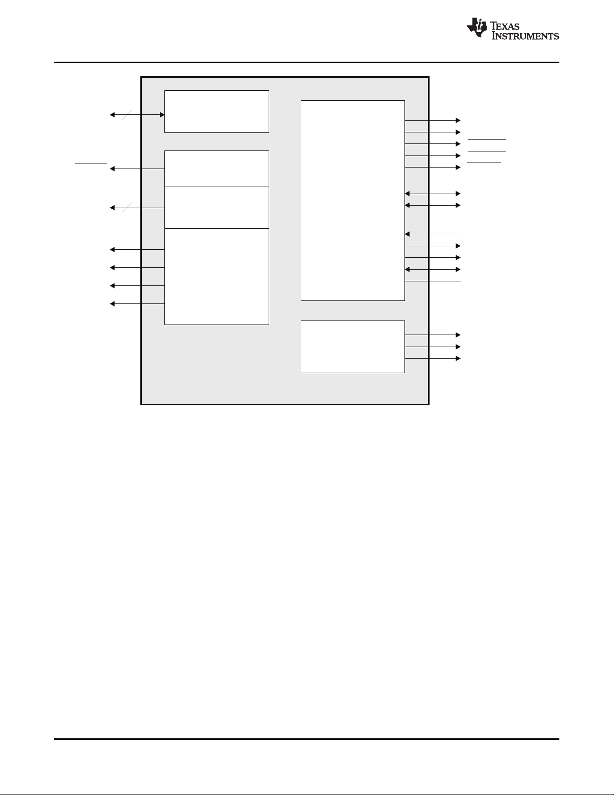
2.6 Signal Groups Description
TMS320C6474
SPRS552F–OCTOBER 2008–REVISED JULY 2010
Figure 2-6. CPU and Peripheral Signals
Copyright © 2008–2010, Texas Instruments Incorporated Device Overview 21
Submit Documentation Feedback
Product Folder Link(s) :TMS320C6474
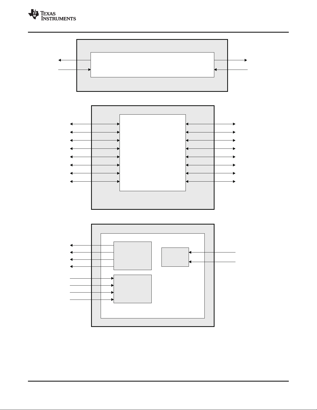
Page 22
DDRD[31:0]
DDRCE
DDRA[13:0]
14
DDRDQM0
DDRDQM1
DDRDQM2
DDRDQM3
Data
MemoryMap
Address
ByteEnables
DDRCLKOUTP
DDRCLKOUTN
DDRCAS
DDRRAS
DDRWE
DDRDQSP[3:0]
DDRDQSN[3:0]
DDRRCVENIN[2:0]
DDRRCVENOUT[2:0]
DDRODT
DDRSLRATE
V
REFSSTL
DDRBA0
DDRBA1
DDRBA2
External
Memory
Controller
Bank Address
DDRMemoryController(32-bitDataBus)
32
TMS320C6474
SPRS552F–OCTOBER 2008–REVISED JULY 2010
www.ti.com
Figure 2-7. DDR Memory Controller Peripheral Signals
22 Device Overview Copyright © 2008–2010, Texas Instruments Incorporated
Submit Documentation Feedback
Product Folder Link(s) :TMS320C6474
Page 23
TIMI0
TIMO0
GP00
GP01
GP02
GP03
GP04
GP05
GP06
GP07
RIOTXN0
RIOTXP0
RIOTXN1
RIOTXP1
RIORXN0
RIORXP0
RIORXN1
RIORXP1
Transmit
Receive
Clock
RapidIO
RIOSGMIICLKP
(A)
RIOSGMIICLKN
(A)
GP08
GP09
GP10
GP11
GP12
GP13
GP14
GP15
GPIO
General-PurposeInput/Output0(GPIO)Port
TIMO1
TIMI1
TimerPinManager
Timers(64-Bit)
www.ti.com
TMS320C6474
SPRS552F–OCTOBER 2008–REVISED JULY 2010
A. Reference Clock to drive RapidIO and SGMII.
Figure 2-8. Timers/GPIO/RapidIO Peripheral Signals
Copyright © 2008–2010, Texas Instruments Incorporated Device Overview 23
Submit Documentation Feedback
Product Folder Link(s) :TMS320C6474
Page 24
CLKX1
FSX1
DX1
CLKR1
FSR1
DR1
CLKS1
CLKX0
FSX0
DX0
CLKR0
FSR0
DR0
CLKS0
McBSP1
Clock
Receive
Transmit
McBSP0
Clock
Receive
Transmit
MultichannelBufferedSerialPorts
(McBSPs)
FRAMEBURSTN
FRAMEBURSTP
ALTFSYNCPULSE
TRT
FSYNCCLKN
FSYNCCLKP
ALTFSYNCCLK
TRTCLK
SMFRAMECLK
FSYNC Clock
FrameSynchroniztion(FSYNC)
AIFTXN[5:0]
AIFTXP[5:0]
AIFRXN[5:0]
AIFRXP[5:0]
SCL
SDA
Transmit
SCL
Receive
AntennaInterface(AIF)
I2C
TMS320C6474
SPRS552F–OCTOBER 2008–REVISED JULY 2010
www.ti.com
Figure 2-9. McBSP/FSYNC/AIF/I2C Peripheral Signals
24 Device Overview Copyright © 2008–2010, Texas Instruments Incorporated
Submit Documentation Feedback
Product Folder Link(s) :TMS320C6474
Page 25
SGMIITXN
SGMIITXP
SGMIIRXN
SGMIIRXP
RIOSGMIICLKN
(A)
RIOSGMIICLKP
(A)
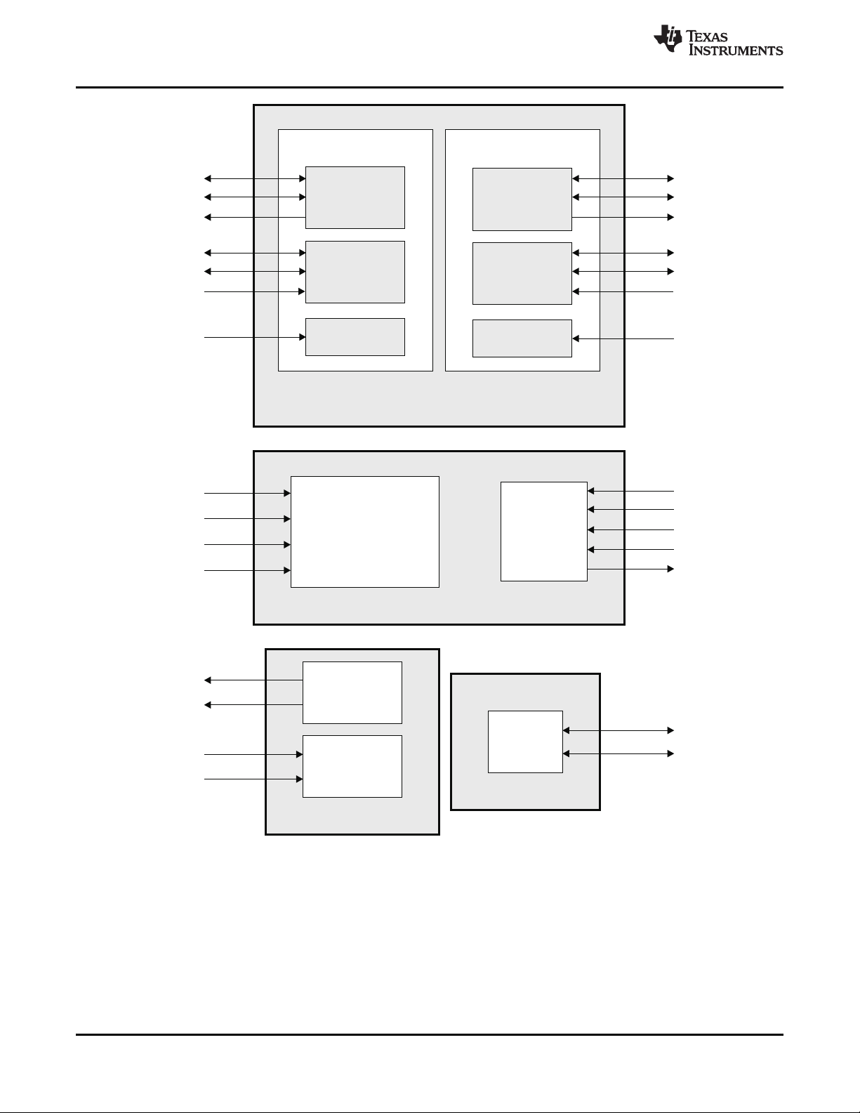
EthernetMAC
(EMAC)
SGMII
Transmit
SGMII
Receive
SGMII
Clock
MDIO
EthernetMAC(EMAC)andMDIO
MDIO
MDCLK
www.ti.com
TMS320C6474
SPRS552F–OCTOBER 2008–REVISED JULY 2010
A. Reference Clock to drive RapidIO and SGMII.
Figure 2-10. EMAC/MDIO [SGMII] Peripheral Signals
Copyright © 2008–2010, Texas Instruments Incorporated Device Overview 25
Submit Documentation Feedback
Product Folder Link(s) :TMS320C6474
Page 26
TMS320C6474
SPRS552F–OCTOBER 2008–REVISED JULY 2010
2.7 Terminal Functions
The terminal functions table (Table 2-5) identifies the external signal names, the pin type (I, O, O/Z, or
I/O/Z), whether the pin has any internal pullup/pulldown resistors, and the signal function description.
Table 2-5. Terminal Functions
SIGNAL
NAME NO.
AIFRXN0 AF22 I
AIFRXP0 AF21 I
AIFRXN1 AG20 I
AIFRXP1 AG21 I
AIFRXN2 AG18 I
AIFRXP2 AG17 I
AIFRXN3 AE17 I
AIFRXP3 AE18 I
AIFRXN4 AE14 I
AIFRXP4 AE13 I
AIFRXN5 AF12 I
AIFRXP5 AF13 I
AIFTXN0 AE21 O
AIFTXP0 AE22 O
AIFTXN1 AD21 O
AIFTXP1 AD20 O
AIFTXN2 AF16 O
AIFTXP2 AF17 O
AIFTXN3 AD17 O
AIFTXP3 AD16 O
AIFTXN4 AG13 O
AIFTXP4 AG14 O
AIFTXN5 AD13 O
AIFTXP5 AD12 O
NMI0 J4 I IPD Non-maskable interrupts. NMI0, NMI1, and NMI2 pins are mapped to C64x+
NMI1 J2 I IPD
NMI2 J1 I IPD
XWRST AD5 I Warm Reset
RESETSTAT AF4 O Reset Status Output
POR AE5 I Power-on Reset
SYSCLKP AE9 I
SYSCLKN AE10 I
ALTCORECLKN AF10 I
ALTCORECLKP AF9 I
DDRREFCLKN AD23 I
DDRREFCLKP AD24 I
SYSCLKOUT AD6 O/Z IPD
TYPE
(1)
IPD/IPU
(2)
ANTENNA INTERFACE
Antenna Interface Receive Data (6 links)
Antenna Interface Transmit Data (6 links)
CLOCK/RESETS
Megamodule Core 0, C64x+ Megamodule Core 1, and C64x+ Megamodule Core
2, respectively. NMIs are edge-driven (rising edge). Any noise on the NMI pin
may trigger an NMI interrupt; therefore, if the NMI pin is not used, it is
recommended that the NMI pin be grounded rather than relying on the IPD.
System Clock Input to Antenna Interface and main PLL (Main PLL optional vs
ALTCORECLK)
Alternate Core Clock Input to main PLL (vs SYSCLK)
DDR Reference Clock Input to DDR PLL
System Clock Output to be used as a general purpose output clock for debug
purposes
SIGNAL DESCRIPTION
www.ti.com
(1) I = Input, O = Output, Z = High impedance, S = Supply voltage, GND = Ground, A = Analog signal
(2) IPD = internal pulldown, IPU = internal pullup. All internal pullups and pulldowns are 100 mA.
26 Device Overview Copyright © 2008–2010, Texas Instruments Incorporated
Submit Documentation Feedback
Product Folder Link(s) :TMS320C6474
Page 27
www.ti.com
Table 2-5. Terminal Functions (continued)
SIGNAL
NAME NO.
CORECLKSEL AF7 I
RIOSGMIICLKN D9 I
RIOSGMIICLKP C9 I
DDRDQM0 W24 O/Z
DDRDQM1 AE24 O/Z
DDRDQM2 B24 O/Z
DDRDQM3 H24 O/Z
DDRCE L24 O/Z DDR2 EMIF Chip Enable
DDRBA0 T25 O/Z
DDRBA1 R25 O/Z DDR Bank Address
DDRBA2 U25 O/Z
DDRA00 K25 O/Z
DDRA01 N25 O/Z
DDRA02 M25 O/Z
DDRA03 R26 O/Z
DDRA04 L25 O/Z
DDRA05 N27 O/Z
DDRA06 L26 O/Z
DDRA07 U26 O/Z
DDRA08 K26 O/Z
DDRA09 R27 O/Z
DDRA10 P25 O/Z
DDRA11 L27 O/Z
DDRA12 U27 O/Z
DDRA13 K27 O/Z
DDRCLKOUTP0 V25 O/Z
DDRCLKOUTN0 V24 O/Z
DDRCLKOUTP1 J25 O/Z
DDRCLKOUTN1 J24 O/Z
TYPE
(1)
(2)
IPD/IPU
Core Clock Select to select between SYSCLK(N|P) and ALTCORECCLK to the
main PLL
RapidIO/SGMII Reference Clock to drive the RapidIO and SGMII SERDES
DDR MEMORY CONTROLLER
DDR2 EMIF Data Masks
DDR2 EMIF Address Bus
DDR2 EMIF Output Clocks to drive SDRAMs (one clock pair per SDRAM)
TMS320C6474
SPRS552F–OCTOBER 2008–REVISED JULY 2010
SIGNAL DESCRIPTION
Copyright © 2008–2010, Texas Instruments Incorporated Device Overview 27
Submit Documentation Feedback
Product Folder Link(s) :TMS320C6474
Page 28
TMS320C6474
SPRS552F–OCTOBER 2008–REVISED JULY 2010
Table 2-5. Terminal Functions (continued)
SIGNAL
NAME NO.
DDRD00 W27 I/O/Z
DDRD01 W25 I/O/Z
DDRD02 Y27 I/O/Z
DDRD03 W26 I/O/Z
DDRD04 AA27 I/O/Z
DDRD05 AA26 I/O/Z
DDRD06 AA25 I/O/Z
DDRD07 AA24 I/O/Z
DDRD08 AC27 I/O/Z
DDRD09 AC26 I/O/Z
DDRD10 AC25 I/O/Z
DDRD11 AD27 I/O/Z
DDRD12 AC24 I/O/Z
DDRD13 AE26 I/O/Z
DDRD14 AE27 I/O/Z
DDRD15 AE25 I/O/Z
DDRD16 B25 I/O/Z
DDRD17 D25 I/O/Z
DDRD18 B26 I/O/Z
DDRD19 D24 I/O/Z
DDRD20 B27 I/O/Z
DDRD21 D26 I/O/Z
DDRD22 D27 I/O/Z
DDRD23 C27 I/O/Z
DDRD24 F24 I/O/Z
DDRD25 F25 I/O/Z
DDRD26 F26 I/O/Z
DDRD27 F27 I/O/Z
DDRD28 G27 I/O/Z
DDRD29 H25 I/O/Z
DDRD30 H26 I/O/Z
DDRD31 H27 I/O/Z
DDRCAS N26 O/Z DDR2 EMIF Column Address Strobe
DDRRAS M24 O/Z DDR2 Row Address Strobe
DDRWE P24 O/Z DDR2 EMIF Write Enable
DDRCKE T24 O/Z DDR2 EMIF Clock Enable
DDRDQS0P Y26 I/O/Z
DDRDQS0N Y25 I/O/Z
DDRDQS1P AD26 I/O/Z
DDRDQS1N AD25 I/O/Z
DDRDQS2P C26 I/O/Z
DDRDQS2N C25 I/O/Z
DDRDQS3P G25 I/O/Z
DDRDQS3N G26 I/O/Z
TYPE
(1)
IPD/IPU
(2)
DDR2 EMIF Data Bus
DDR2 EMIF Data Strobe
SIGNAL DESCRIPTION
www.ti.com
28 Device Overview Copyright © 2008–2010, Texas Instruments Incorporated
Submit Documentation Feedback
Product Folder Link(s) :TMS320C6474
Page 29
TMS320C6474
www.ti.com
Table 2-5. Terminal Functions (continued)
SIGNAL
NAME NO.
DDRRCVENIN0 AB25 I
DDRRCVENOUT0 AB24 O/Z
DDRRCVENIN1 E24 I
DDRRCVENOUT1 E25 O/Z
DDRODT K24 O/Z Bits 1:0 are the ODT status, these bits are Read/Write:
DDRSLRATE AE23 I DDR2 Slew rate control
V
REFSSTL
T26 A Reference Voltage Input for SSTL18 buffers used by DDR2 EMIF (V
TCK W4 I IPU JTAG Clock Input
TDI V4 I IPU JTAG Data Input
TDO W3 O/Z JTAG Data Output
TMS W1 I IPU JTAG Test Mode Input
TRST W2 I IPD JTAG Reset
EMU00 R4 I/O/Z IPU
EMU01 R2 I/O/Z IPU
EMU02 N3 I/O/Z IPU
EMU03 N1 I/O/Z IPU
EMU04 M2 I/O/Z IPU
EMU05 M1 I/O/Z IPU
EMU06 N4 I/O/Z IPU
EMU07 R3 I/O/Z IPU
EMU08 M4 I/O/Z IPU
EMU09 N2 I/O/Z IPU Emulation and Trace Port
EMU10 R1 I/O/Z IPU
EMU11 T2 I/O/Z IPU
EMU12 L3 I/O/Z IPU
EMU13 P4 I/O/Z IPU
EMU14 K2 I/O/Z IPU
EMU15 T1 I/O/Z IPU
EMU16 P3 I/O/Z IPU
EMU17 L4 I/O/Z IPU
EMU18 M3 I/O/Z IPU
FSYNCCLKN AD8 I Frame Sync Interface Clock used to drive the frame synchronization interface
FSYNCCLKP AD7 I
SMFRAMECLK AD4 O/Z IPD Frame Sync Clock Output
FRAMEBURSTN AD10 I
FRAMEBURSTP AD9 I
ALTFSYNCCLK AF6 I IPD Alternate Frame Sync Clock Input (vs FSYNCCLK(N|P)
ALTFSYNCPULSE AE6 I IPD Alternate Frame Sync Input (vs FRAMEBURST (N|P)
TRT AD3 I IPD Multi-standard Frame Synchronization Tick
TRTCLK AC4 I IPD Multi-standard Frame Synchronization Clock
TYPE
(1)
(2)
IPD/IPU
DDR2 EMIF Data Strobe Gate Input/Outputs to help meet DDR Timing
DDR2 EMIF On-Die Termination Outputs used to set termination on the
SDRAMs
The DDR2 ODT control register is found at 0x7000 00F0
00 - no termination
01- half termination
11 - full termination
JTAG EMULATION
FRAME SYNCHRONIZATION (FSYNC)
(OBSAI RP1 clock)
Frame Burst to drive frame indicators to the frame synchronization module
(OBSAI RP1)
SPRS552F–OCTOBER 2008–REVISED JULY 2010
SIGNAL DESCRIPTION
DDS18/2
)
Copyright © 2008–2010, Texas Instruments Incorporated Device Overview 29
Submit Documentation Feedback
Product Folder Link(s) :TMS320C6474
Page 30
TMS320C6474
SPRS552F–OCTOBER 2008–REVISED JULY 2010
Table 2-5. Terminal Functions (continued)
SIGNAL
NAME NO.
GP00 T3 I/O/Z IPD
GP01 U4 I/O/Z IPD
GP02 V1 I/O/Z IPD
GP03 U3 I/O/Z IPD
GP04 T4 I/O/Z IPU
GP05 V2 I/O/Z IPD
GP06 V3 I/O/Z IPD
GP07 Y3 I/O/Z IPD
GP08 Y4 I/O/Z IPD
GP09 AA2 I/O/Z IPD
GP10 AA3 I/O/Z IPD
GP11 AB4 I/O/Z IPD
GP12 AB3 I/O/Z IPD
GP13 AB2 I/O/Z IPD
GP14 AA4 I/O/Z IPD
GP15 AC3 I/O/Z IPD
SCL E4 I/O/Z I2C Clock (open drain)
SDA D4 I/O/Z I2C Data (open drain)
CLKS0 D20 I IPD McBSP0 Module Clock
CLKR0 B20 I/O/Z IPD McBSP0 Receive Clock
CLKX0 C20 I/O/Z IPD McBSP0 Transmit Clock
DR0 A20 I IPD McBSP0 Receive Data
DX0 D19 O/Z IPD McBSP0 Transmit Data
FSR0 B21 I/O/Z IPD McBSP0 Receive Frame Sync
FSX0 A21 I/O/Z IPD McBSP0 Transmit Frame Sync
CLKS1 A25 I IPD McBSP1 Module Clock
CLKR1 A24 I/O/Z IPD McBSP1 Receive Clock
CLKX1 C22 I/O/Z IPD McBSP1 Transmit Clock
DR1 D21 I IPD McBSP1 Receive Data
DX1 B22 O/Z IPD McBSP1 Transmit Data
FSR1 C21 I/O/Z IPD McBSP1 Receive Frame Sync
FSX1 A22 I/O/Z IPD McBSP1 Transmit Frame Sync
VCNTL0 G3 O
VCNTL1 G2 O
VCNTL2 H4 O
VCNTL3 H3 O
RIORXN0 A9 I
RIORXP0 A10 I
RIORXN1 A13 I
RIORXP1 A12 I
(1)
TYPE
GENERAL PURPOSE INPUT/OUTPUT (GPIO)
MULTICHANNEL BUFFERED SERIAL PORT (McBSP)
IPD/IPU
(2)
General Purpose Input/Output
GPIO[3:0] are mapped to BOOTMODE[3:0]
(see Section 2.4.1, Boot Modes Supported)
GPIO4 is mapped to LENDIAN
0 = Big Endian
1 = Little Endian (default)
GPIO5 is mapped to L2_CONFIG is a reserved bootstrap pin and should be
pulled up to DV
during bootstrap
GPIO[7:6] are not multiplexed
GPIO[11:8] are mapped to DEVNUM[3:0]
(see Section 2.4.1, Boot Modes Supported)
GPIO[15:12] are not multiplexed
MISCELLANEOUS
Voltage Control Outputs to variable core power supply (open-drain buffers)
Note: These pins must be externally pulled up. For more infomation, see the
TMS320C6474 Hardware Design Guide application report (literature number
SPRAAW7).
SERIAL RAPIDIO (SRIO)
Serial RapidIO Receive Data (2 links)
DD18
I2C
www.ti.com
SIGNAL DESCRIPTION
30 Device Overview Copyright © 2008–2010, Texas Instruments Incorporated
Submit Documentation Feedback
Product Folder Link(s) :TMS320C6474
Page 31

www.ti.com
Table 2-5. Terminal Functions (continued)
SIGNAL
NAME NO.
RIOTXN0 C11 O
RIOTXP0 C10 O
RIOTXN1 C13 O
RIOTXP1 C14 O
SGMIIRXN C16 I
SGMIIRXP C17 I
SGMIITXN A16 O
SGMIITXP A15 O
MDIO B19 I/O/Z IPU MDIO Data
MDCLK C19 O IPD MDIO Clock
TIMI0 E3 I IPD
TIMI1 C4 I IPD
TIMO0 F2 O/Z IPD
TIMO1 F4 O/Z IPD
RSV01 AE19 A Reserved, unconnected
RSV02 AD14 A Reserved, unconnected
RSV03 N24 A Reserved, 45.3-Ω 1% resistor to GND
RSV04 AG10 A Reserved, unconnected
RSV05 AG24 A Reserved, unconnected
RSV06 AE7 O Reserved, unconnected
RSV07 AE8 O Reserved, unconnected
RSV08 AF24 O Reserved, unconnected
RSV09 AF25 O Reserved, unconnected
RSV10 K4 I/O/Z IPU Reserved, unconnected
RSV11 K3 I/O/Z IPU Reserved, unconnected
RSV12 K1 I/O/Z IPU Reserved, unconnected
RSV13 G4 O/Z IPD Reserved, unconnected
RSV14 F3 O/Z IPD Reserved, unconnected
RSV15 D7 A Reserved, GND connection
RSV16 C7 A Reserved, unconnected
RSV17 B12 A Reserved, unconnected
RSV18 B18 A Reserved, unconnected
RSV19 D6 I/O/Z IPU Reserved, unconnected
RSV20 C6 I/O/Z IPU Reserved, unconnected
RSV21 E6 Reserved, CVDDconnection
RSV22 E7 Reserved, CVDDconnection
RSV23 AE4 O/Z IPD Reserved, unconnected
RSV24 AG25 O/Z IPD Reserved, unconnected
RSV25 D22 A Reserved, GND connection
RSV26 C23 A Reserved, GND connection
RSV27 D5 A Reserved, unconnected
RSV28 C5 A Reserved, unconnected
TYPE
(1)
MANAGEMENT DATA INPUT/OUTPUT (MDIO)
(2)
IPD/IPU
Serial RapidIO Transmit data (2 links)
ETHERNET MAC (EMAC) AND SGMII
Ethernet MAC SGMII Receive Data
Ethernet MAC SGMII Transmit Data
TIMERS
Timer Inputs
Timer Outputs
RESERVED
SIGNAL DESCRIPTION
TMS320C6474
SPRS552F–OCTOBER 2008–REVISED JULY 2010
Copyright © 2008–2010, Texas Instruments Incorporated Device Overview 31
Submit Documentation Feedback
Product Folder Link(s) :TMS320C6474
Page 32

TMS320C6474
SPRS552F–OCTOBER 2008–REVISED JULY 2010
Table 2-5. Terminal Functions (continued)
SIGNAL
NAME NO.
RSV29 J3 Reserved, DV
J11 S
J17 S
J19 S
J9 S
K10 S
K18 S
L11 S
L13 S
L15 S
L17 S
L19 S
L9 S
M10 S
M12 S
M14 S
M16 S
M18 S
N11 S
CV
DD
N13 S 0.9 - 1.2-V Core Supply Voltage
N15 S
N17 S
N19 S
N9 S
P10 S
P12 S
P14 S
P16 S
P18 S
R11 S
R13 S
R15 S
R17 S
R19 S
R9 S
T10 S
T12 S
T14 S
TYPE
(1)
IPD/IPU
(2)
SUPPLY VOLTAGE PINS
DD18
www.ti.com
SIGNAL DESCRIPTION
connection
32 Device Overview Copyright © 2008–2010, Texas Instruments Incorporated
Submit Documentation Feedback
Product Folder Link(s) :TMS320C6474
Page 33

www.ti.com
SIGNAL
NAME NO.
CV
DD
AIF_V
DDA11
SGR_V
DDA11
AV
DD218
AV
DD118
AIF _V
DDD11
SGR_V
DDD11
CV
DDMON
AIF_V
DDR18
SGR_V
DDR18
SPRS552F–OCTOBER 2008–REVISED JULY 2010
Table 2-5. Terminal Functions (continued)
(1)
TYPE
T16 S
T18 S
U11 S
U13 S
U15 S
U19 S
U9 S 0.9 - 1.2-V Core Supply Voltage
V10 S
V12 S
V14 S
W11 S
W13 S
W9 S
AC12 A
AC15 A
AC18 A
AC21 A
D12 A
D18 A
E11 A
E15 A
AG23 A
AG9 A
AG26 S
U17 S
V16 S
V18 S 1.1-V AIF Serdes Digital Supply
W15 S
W17 S
W19 S
J13 S
J15 S
K12 S 1.1-V SRIO/SGMII Serdes Digital Supply
K14 S
K16 S
AG6 S 0.9 - 1.2-V CVDDSupply Monitor
AD19 S
AD15 S
C12 S
A18 S
IPD/IPU
(2)
SIGNAL DESCRIPTION
1.1-V AIF Serdes Analog Supply
1.1-V SRIO/SGMII Serdes Analog Supply
1.8-V PLL Supply
1.8-V AIF Serdes Regulator Supply
1.8-V SRIO/SGMII Serdes Regulator Supply
TMS320C6474
Copyright © 2008–2010, Texas Instruments Incorporated Device Overview 33
Submit Documentation Feedback
Product Folder Link(s) :TMS320C6474
Page 34

TMS320C6474
SPRS552F–OCTOBER 2008–REVISED JULY 2010
Table 2-5. Terminal Functions (continued)
SIGNAL
NAME NO.
DV
DD18
A1 S
A19 S
A23 S
A27 S
A5 S
AA23 S
AA5 S
AB26 S
AC1 S
AC23 S
AC5 S
AC7 S
AC9 S
AF5 S
AG1 S
AG27 S
AG8 S
E1 S
E19 S
E21 S
E23 S
E27 S 1.8-V I/O Supply
E5 S
G23 S
G5 S
H2 S
J23 S
J27 S
J5 S
L1 S
L23 S
L5 S
M26 S
N23 S
N5 S
P2 S
P26 S
R23 S
R5 S
U1 S
U23 S
U5 S
V26 S
TYPE
(1)
IPD/IPU
www.ti.com
(2)
SIGNAL DESCRIPTION
34 Device Overview Copyright © 2008–2010, Texas Instruments Incorporated
Submit Documentation Feedback
Product Folder Link(s) :TMS320C6474
Page 35

www.ti.com
SIGNAL
NAME NO.
DV
DD18
DV
DD18MON
AIF_V
DDT11
SGR_V
DDT11
Table 2-5. Terminal Functions (continued)
(1)
TYPE
W23 S
W5 S
Y2 S
Y24 S
AG7 S 1.8-V DV
AC11 S
AC14 S
AC17 S
AC20 S 1.1-V AIF Serdes Termination Supply
AF15 S
AF19 S
AG11 S
B13 S
B17 S
B8 S
E13 S
E17 S
E9 S
IPD/IPU
(2)
SIGNAL DESCRIPTION
1.8-V I/O Supply
Supply Monitor
DD18
1.1-V SRIO/SGMII Serdes Termination Supply
TMS320C6474
SPRS552F–OCTOBER 2008–REVISED JULY 2010
Copyright © 2008–2010, Texas Instruments Incorporated Device Overview 35
Submit Documentation Feedback
Product Folder Link(s) :TMS320C6474
Page 36

TMS320C6474
SPRS552F–OCTOBER 2008–REVISED JULY 2010
Table 2-5. Terminal Functions (continued)
SIGNAL
NAME NO.
V
SS
A11
A14
A17
A2
A26
A3
A4
A6
A7
A8
AA1
AB1
AB23
AB27
AB5
AC10
AC13
AC16
AC19
AC2
AC22
AC6 GND Ground
AC8
AD1
AD11
AD18
AD2
AD22
AE1
AE11
AE12
AE15
AE16
AE2
AE20
AE3
AF1
AF11
AF14
AF18
AF2
AF20
AF23
TYPE
(1)
IPD/IPU
(2)
www.ti.com
SIGNAL DESCRIPTION
GROUND PINS
36 Device Overview Copyright © 2008–2010, Texas Instruments Incorporated
Submit Documentation Feedback
Product Folder Link(s) :TMS320C6474
Page 37

www.ti.com
SIGNAL
NAME NO.
V
SS
Table 2-5. Terminal Functions (continued)
(1)
TYPE
AF26
AF27
AF3
AF8
AG12
AG15
AG16
AG19
AG2
AG22
AG3
AG4
AG5
B1
B10
B11
B14
B15
B16
B2
B23
B3 GND Ground
B4
B5
B6
B7
B9
C1
C15
C18
C2
C24
C3
C8
D1
D10
D11
D13
D14
D15
D16
D17
D2
IPD/IPU
(2)
TMS320C6474
SPRS552F–OCTOBER 2008–REVISED JULY 2010
SIGNAL DESCRIPTION
Copyright © 2008–2010, Texas Instruments Incorporated Device Overview 37
Submit Documentation Feedback
Product Folder Link(s) :TMS320C6474
Page 38

TMS320C6474
SPRS552F–OCTOBER 2008–REVISED JULY 2010
Table 2-5. Terminal Functions (continued)
SIGNAL
NAME NO.
V
SS
D23
D3
D8
E10
E12
E14
E16
E18
E2
E20
E22
E26
E8
F1
F23
F5
G1
G24
H1
H23
H5
J10 GND Ground
J12
J14
J16
J18
J26
K11
K13
K15
K17
K19
K23
K5
K9
L10
L12
L14
L16
L18
L2
M11
M13
TYPE
(1)
IPD/IPU
www.ti.com
(2)
SIGNAL DESCRIPTION
38 Device Overview Copyright © 2008–2010, Texas Instruments Incorporated
Submit Documentation Feedback
Product Folder Link(s) :TMS320C6474
Page 39

www.ti.com
SIGNAL
NAME NO.
V
SS
Table 2-5. Terminal Functions (continued)
(1)
TYPE
M15
M17
M19
M23
M27
M5
M9
N10
N12
N14
N16
N18
P1
P11
P13
P15
P17
P19
P23
P27
P5
P9 GND Ground
R10
R12
R14
R16
R18
R24
T11
T13
T15
T17
T19
T23
T27
T5
T9
U10
U12
U14
U16
U18
U2
IPD/IPU
(2)
TMS320C6474
SPRS552F–OCTOBER 2008–REVISED JULY 2010
SIGNAL DESCRIPTION
Copyright © 2008–2010, Texas Instruments Incorporated Device Overview 39
Submit Documentation Feedback
Product Folder Link(s) :TMS320C6474
Page 40

TMS320C6474
SPRS552F–OCTOBER 2008–REVISED JULY 2010
Table 2-5. Terminal Functions (continued)
SIGNAL
NAME NO.
V
SS
U24
V11
V13
V15
V17
V19
V23
V27
V5
V9
W10
W12
W14
W16
W18
Y1
Y23
Y5
(1)
TYPE
GND Ground
IPD/IPU
www.ti.com
(2)
SIGNAL DESCRIPTION
40 Device Overview Copyright © 2008–2010, Texas Instruments Incorporated
Submit Documentation Feedback
Product Folder Link(s) :TMS320C6474
Page 41

TMS320C6474
www.ti.com
2.8 Development
2.8.1 Development Support
In case the customer would like to develop their own features and software on the C6474 device, TI offers
an extensive line of development tools for the TMS320C6000 DSP platform, including tools to evaluate the
performance of the processors, generate code, develop algorithm implementations, and fully integrate and
debug software and hardware modules. The tool's support documentation is electronically available within
the Code Composer Studio™ Integrated Development Environment (IDE). The following products support
development of C6000 DSP-based applications:
Software Development Tools: Code Composer Studio Integrated Development Environment (IDE):
including Editor C/C++/Assembly Code Generation, and Debug plus additional development tools
Scalable, Real-Time Foundation Software (DSP/BIOS™), which provides the basic run-time target
software needed to support any DSP application.
Hardware Development Tools: Extended Development System (XDS™) Emulator (supports C6000 DSP
multiprocessor system debug) Evaluation Module (EVM).
2.8.2 Device Support
2.8.2.1 Device and Development-Support Tool Nomenclature
To designate the stages in the product development cycle, TI assigns prefixes to the part numbers of all
DSP devices and support tools. Each DSP commercial family member has one of three prefixes: TMX,
TMP, or TMS (e.g., TMS320C6474ZUN). Texas Instruments recommends two of three possible prefix
designators for its support tools: TMDX and TMDS. These prefixes represent evolutionary stages of
product development from engineering prototypes (TMX/TMDX) through fully qualified production
devices/tools (TMS/TMDS).
SPRS552F–OCTOBER 2008–REVISED JULY 2010
Device development evolutionary flow:
• TMX: Experimental device that is not necessarily representative of the final device's electrical
specifications.
• TMP: Final silicon die that conforms to the device's electrical specifications but has not completed
quality and reliability verification.
• TMS: Fully qualified production device.
Support tool development evolutionary flow:
• TMDX: Development-support product that has not yet completed Texas Instruments internal
qualification testing.
• TMDS: Fully qualified development-support product .
TMX and TMP devices and TMDX development-support tools are shipped with against the following
disclaimer:
"Developmental product is intended for internal evaluation purposes."
TMS devices and TMDS development-support tools have been characterized fully, and the quality and
reliability of the device have been demonstrated fully. TI's standard warranty applies.
Predictions show that prototype devices (TMX or TMP) have a greater failure rate than the standard
production devices. Texas Instruments recommends that these devices not be used in any production
system because their expected end-use failure rate still is undefined. Only qualified production devices are
to be used.
Copyright © 2008–2010, Texas Instruments Incorporated Device Overview 41
Submit Documentation Feedback
Product Folder Link(s) :TMS320C6474
Page 42

C64x+ DSP:
C6474
PREFIX
TMS 320
C6474
ZUN
TMX = Experimental device
TMS = Qualified device
DEVICE FAMILY
320 = TMS320 DSP familyä
PACKAGE TYPE
(B)
CUN = 561-pin plastic BGA (lead-free die bump and solder balls)
GUN = 561-pin plastic BGA (leaded [Pb] solder balls)
ZUN = 561-pin plastic BGA (lead-free solder balls and leaded [Pb] die bumps)
DEVICE
DEVICE SPEED RANGE
Blank = 1 GHz
2 = 1.2 GHz
8 = 850 MHz
( )
TEMPERATURE RANGE
Blank = 0 C to 100 C (default commercial temperature; 850-MHz and 1-GHz device)
Blank = 0°C to 95°C (default commercial temperature; 1.2-GHz device)
A = -40°C to 100°C (extended temperature; 1-GHz device)
A = (extended temperature; 1.2-GHz device)
° °
-40°C to 95°C
( )
( )
SILICON REVISION
(A)
F = Silicon Revision 2.1
TMS320C6474
SPRS552F–OCTOBER 2008–REVISED JULY 2010
TI device nomenclature also includes a suffix with the device family name. This suffix indicates the
package type (for example, ZUN), the temperature range (for example, Blank is the default commercial
temperature range), and the device speed range in megahertz (for example, Blank is 1000 [1 GHz]).
Figure 2-11 provides a legend for reading the complete device name for any TMS320C64x+ DSP
generation member. For device part numbers and further ordering information for TMS320C6474 in the
CUN, GUN, or ZUN package type, see the TI website (www.ti.com) or contact your TI sales
representative.
A. Silicon revision correlates to the lot trace code found on the second line of the package marking. For more
information, see the TMS320C6474 Digital Signal Processor Silicon Errata (literature number SPRZ283).
B. BGA = Ball Grid Array
Figure 2-11. TMS320C64x+™ DSP Device Nomenclature (including TMS320C6474 DSP)
www.ti.com
2.8.2.2 Documentation Support
42 Device Overview Copyright © 2008–2010, Texas Instruments Incorporated
The following documents describe the TMS320C6474 multicore digital signal processor. Copies of these
documents are available on the Internet at www.ti.com. Tip: Enter the literature number in the search box
provided at www.ti.com.
SPRU732 TMS320C64x/C64x+ DSP CPU and Instruction Set Reference Guide. Describes the CPU
architecture, pipeline, instruction set, and interrupts for the TMS320C64x and TMS320C64x+
digital signal processors (DSPs) of the TMS320C6000 DSP family. The C64x/C64x+ DSP
generation comprises fixed-point devices in the C6000 DSP platform. The C64x+ DSP is an
enhancement of the C64x DSP with added functionality and an expanded instruction set.
SPRU871 TMS320C64x+ DSP Megamodule Reference Guide. Describes the TMS320C64x+ digital
signal processor (DSP) megamodule. Included is a discussion on the internal direct memory
access (IDMA) controller, the interrupt controller, the power-down controller, memory
protection, bandwidth management, and the memory and cache.
SPRAA84 TMS320C64x to TMS320C64x+ CPU Migration Guide. Describes migrating from the Texas
Instruments TMS320C64x digital signal processor (DSP) to the TMS320C64x+ DSP. The
objective of this document is to indicate differences between the two cores. Functionality in
the devices that is identical is not included.
SPRU889 High-Speed DSP Systems Design Reference Guide. Provides recommendations for
meeting the many challenges of high-speed DSP system design. These recommendations
include information about DSP audio, video, and communications systems for the C5000 and
C6000 DSP platforms.
SPRUG08 TMS320C6474 DSP Ethernet Media Access Controller (EMAC)/ Management Data
Input/Output (MDIO) User's Guide. This document provides a functional description of the
Ethernet Media Access Controller (EMAC) and Physical layer (PHY) device Management
Data Input/Output (MDIO) module integrated with the TMS320C6474 digital signal
Submit Documentation Feedback
Product Folder Link(s) :TMS320C6474
Page 43

TMS320C6474
www.ti.com
processors (DSPs).
SPRUG09 TMS320C6474 DSP Software-Programmable Phase-Locked Loop (PLL) Controller
User's Guide. This document describes the operation of the software-programmable
phase-locked loop (PLL) controller in the TMS320C6474 digital signal processors (DSPs).
SPRUG10 TMS320C6474 DSP PSC User's Guide. This document describes the Power/Sleep
Controller (PSC) for the TMS320C6474 digital signal processors (DSPs).
SPRUG11 TMS320C6474 DSP Enhanced DMA (EDMA3) Controller User's Guide. This document
describes the Enhanced DMA (EDMA3) Controller on the TMS320C6474 digital signal
processors (DSPs).
SPRUG12 TMS320C6474 DSP Antenna Interface User's Guide. This document describes the
Antenna Interface module on the TMS320C6474 digital signal processors (DSPs).
SPRUG13 TMS320C6474 DSP Frame Synchronization User's Guide. This document describes the
reference guide for Frame Synchronization module on the TMS320C6474 digital signal
processors (DSPs).
SPRUG14 TMS320C6474 DSP Semaphore User's Guide. This document describes the usage of the
semaphore and some of the CSL calls used to configure/use the Semaphore module on the
TMS320C6474 digital signal processors (DSPs).
SPRUG16 TMS320C6474 DSP General-Purpose Input/Output (GPIO) User's Guide. This document
describes the general-purpose input/output (GPIO) peripheral in the digital signal processors
(DSPs) of the TMS320C6474 DSP family.
SPRS552F–OCTOBER 2008–REVISED JULY 2010
SPRUG17 TMS320C6474 DSP Multichannel Buffered Serial Port (McBSP) Reference Guide. This
document describes the operation of the multichannel buffered serial port (McBSP) in the
digital signal processors (DSPs) of the TMS320C6474 device.
SPRUG18 TMS320C6474 DSP 64-Bit Timer User’s Guide. This document provides an overview of the
64-bit timer in the TMS320C6474 digital signal processors (DSPs).
SPRUG19 TMS320C6474 DSP DDR2 Memory Controller User's Guide. This document describes the
DDR2 memory controller in the TMS320C6474 digital signal processors (DSPs).
SPRUG20 TMS320C6474 DSP Viterbi-Decoder Coprocessor 2 (VCP2) Reference Guide. This
document describes the operation and programming of the VCP2 in the TMS320C6474
digital signal processors (DSPs).
SPRUG21 TMS320C6474 DSP Turbo-Decoder Coprocessor 2 (TCP2) Reference Guide. This
document describes the operation and programming of the TCP2 in the TMS320C6474
digital signal processors (DSPs).
SPRUG22 TMS320C6474 DSP Inter-Integrated Circuit (I2C) Module User's Guide. This document
describes the inter-integrated circuit (I2C) module in the TMS320C6474 digital signal
processors (DSPs).
SPRUG23 TMS320C6474 DSP Serial RapidIO (SRIO) User's Guide. This document describes the
Serial RapidIO (SRIO) on the TMS320C6474 digital signal processors (DSPs).
SPRUEC6 TMS320C645x/C647x DSP Bootloader User's Guide. This document describes the
features of the on-chip Bootloader provided with the TMS320C645x/C647x digital signal
processors (DSPs).
SPRUFK6 TMS320C6474 DSP Chip Interrupt Controller (CIC) User's Guide. This document
describes the system event routing using the chip interrupt controller (CIC) for the
TMS320C6474 digital signal processors (DSPs).
SPRAAW5 TMS320C6474 Module Throughput. This document provides information on the
TMS320C6474 module throughput.
Copyright © 2008–2010, Texas Instruments Incorporated Device Overview 43
Submit Documentation Feedback
Product Folder Link(s) :TMS320C6474
Page 44

TMS320C6474
SPRS552F–OCTOBER 2008–REVISED JULY 2010
SPRAAW7 TMS320C6474 Hardware Design Guide. This document describes hardware system design
considerations for the TMS320C6474 DSP.
SPRAAW8 TMS320C6474 DDR2 Implementation Guidelines. This document provides implementation
instructions for the DDR2 interface contained on the TMS320C6474 DSP.
SPRAAW9 TMS320C6474 SERDES Implementation Guidelines. This document contains
implementation instructions for the three serializer/deserializer (SERDES) based interfaces
on the TMS320C6474 DSP.
SPRAAX3 TMS320C6474 Power Consumption Summary. This document discusses the power
consumption of the Texas Instruments TMS320C6474 digital signal processor (DSP).
SPRAB25 How to Approach Inter-Core Communication on TMS320C6474. This document
discusses the of handling the three cores that are present on the TMS320C6474 DSP along
with what features are supported and how can they be used, how the cores communicate
effectively with each other, and how board-level scalability is allowed.
www.ti.com
44 Device Overview Copyright © 2008–2010, Texas Instruments Incorporated
Submit Documentation Feedback
Product Folder Link(s) :TMS320C6474
Page 45

TMS320C6474
www.ti.com
3 Device Configuration
On the C6474 device, certain device configurations (like boot mode, pin multiplexing, and endianness) are
selected at device reset. The status of the peripherals (enabled/disabled) is determined after device reset.
By default, the peripherals on the device are disabled and must be enabled by software before being
used.
3.1 Device Configuration at Device Reset
Table 3-1 describes the C6474 device. The logic level is latched at reset to determine the device
configuration. The logic level can be set by using external pullup/pulldown resistors or by using some
control device to intelligently drive these pins. When using a control device, take care to avoid contention
on the lines when the device is out of reset. The are sampled during power-on reset and are driven after
the reset is removed. To avoid contention, the control device must stop driving the of the DSP.
NOTE
If a configuration pin must be routed out from the device, the internal pullup/pulldown
(IPU/IPD) resistor should not be relied upon; TI recommends the use of an external
pullup/pulldown resistor.
Table 3-1. Device Configuration Pins
SPRS552F–OCTOBER 2008–REVISED JULY 2010
CONFIGURATION
PIN
BOOTMODE[3:0] 0000b Boot Mode Selection
LENDIAN 1b Device Endian Mode
DEVNUM[3:0] 0000b Device number
CORECLKSEL 0b Core Clock Select
DEFAULT IPU/IPD FUNCTIONAL DESCRIPTION
0 Big Endian
1 Little Endian
0 SYSCLK is shared between the Antenna Interface and the input to PLLCTL1.
1 ALTCORECLK is used as the input to PLLCTL1 and SYSCLK is used only for the
Antenna Interface.
3.2 Peripheral Selection After Device Reset
Several of the peripherals on the C6474 device are controlled by the Power/Sleep Controller (PSC). By
default the AIF, SRIO, TCP, and VCP are held in reset and clock-gated. The memories in these modules
are also in a low-leakage sleep mode. Software will be required to turn these memories on then enable
the modules (turn on clocks and de-assert reset) before these modules can be used.
If one of the above modules is used in the selected boot mode, the ROM code will automatically enable
the used module.
All other modules come up enabled by default and there is no special software sequence to enable.
For more detailed information on the PSC usage, see the TMS320C6474 DSP Power/Sleep Controller
(PSC) User's Guide (literature number SPRUG10).
Copyright © 2008–2010, Texas Instruments Incorporated Device Configuration 45
Submit Documentation Feedback
Product Folder Link(s) :TMS320C6474
Page 46

TMS320C6474
SPRS552F–OCTOBER 2008–REVISED JULY 2010
3.3 Device State Control Registers
The C6474 device has a set of registers that are used to control the status of its peripherals. These
registers are shown in Table 3-2.
Table 3-2. Device State Control Registers
ADDRESS START ADDRESS END SIZE ACRONYM DESCRIPTION
0288 0800 0288 0803 4B DEVCFG1 The first register with the parameters is set through
software to configure different components on the device
0288 0804 0288 0807 4B DEVSTAT Stores all parameters latched from configuration pins or
configured through the DEVCFG register
0288 0808 0288 080B 4B DSP_BOOT_ADDR0 The boot address for C64x+ Megamodule Core 0
0288 080C 0288 080F 4B DSP_BOOT_ADDR1 The boot address for C64x+ Megamodule Core 1
0288 0810 0288 0813 4B DSP_BOOT_ADDR2 The boot address for C64x+ Megamodule Core 2
0288 0814 0288 0817 4B DEVID Parameters for DSP device IDs also referred to as JTAG
or BSDL IDs. These must be readable by the
configuration bus so that this can be accessed via JTAG
and CPU
0288 0818 0288 0827 16B Reserved
0288 0828 0288 082B 4B Reserved
0288 082C 0288 082F 4B Reserved
0288 0830 0288 0833 4B Reserved
0288 0834 0288 083B 8B EFUSE_MAC Required for EMAC boot
0288 083C 0288 083F 4B PRI_ALLOC Priority Allocation Register
0288 0840 0288 08FF 192B Reserved N/A
0288 0900 0288 0903 4B IPCGR0 Register provided to facilitate inter-DSP interrupts and
utilized by hosts or C64x+ Megamodules to generate
interrupts to other DSPs
0288 0904 0288 0907 4B IPCGR1 Register provided to facilitate inter-DSP interrupts and
utilized by hosts or C64x+ Megamodules to generate
interrupts to other DSPs
0288 0908 0288 090B 4B IPCGR2 Register provided to facilitate inter-DSP interrupts and
utilized by hosts or C64x+ Megamodules to generate
interrupts to other DSPs
0288 090C 0288 093F 52B Reserved N/A
0288 0940 0288 0943 4B IPCAR0 Register provided to facilitate inter-DSP interrupts and
utilized by hosts or C64x+ Megamodules to generate
interrupts to other DSPs
0288 0944 0288 0947 4B IPCAR1 Register provided to facilitate inter-DSP interrupts and
utilized by hosts or C64x+ Megamodules to generate
interrupts to other DSPs
0288 0948 0288 094B 4B IPCAR2 Register provided to facilitate inter-DSP interrupts and
utilized by hosts or C64x+ Megamodules to generate
interrupts to other DSPs
www.ti.com
46 Device Configuration Copyright © 2008–2010, Texas Instruments Incorporated
Submit Documentation Feedback
Product Folder Link(s) :TMS320C6474
Page 47

TMS320C6474
www.ti.com
3.4 Device Status Register Descriptions
The device status register depicts the device configuration selected upon device reset. Once set, these
bits remain set until a device reset.
Figure 3-1 shows the device configuration register 1 and Table 3-3 describes the parameters that are set
through software to configure different components on the device. The configuration is done through the
device configuration DEVCFG register, which is one-time writeable through software. The register is reset
on all hard resets and is locked after the first write.
31 3 2 1 0
Reserved CLKS1 CLKS0 SYSCLKOUTEN
R-00000000000000000000000000000 R/W-0 R/W-0 R/W-1
LEGEND: R/W = Read/Write; R = Read only; -n = value after reset
Figure 3-1. Device Configuration Register (DEVCFG)
Table 3-3. Device Configuration Register (DEVCFG) Field Descriptions
Bit Field Value Description
31:3 Reserved Reserved
2 CLKS1 McBSP1 CLKS Select
0 CLKS1 device pin
1 chip_clks from Main.PLL
1 CLKS0 McBSP0 CLKS Select
0 CLKS0 device pin
1 chip_clks from Main.PLL
0 SYSCLKOUTEN SYSCLKOUT Enable
0 No Clock Output
1 Clock output Enabled
SPRS552F–OCTOBER 2008–REVISED JULY 2010
Copyright © 2008–2010, Texas Instruments Incorporated Device Configuration 47
Submit Documentation Feedback
Product Folder Link(s) :TMS320C6474
Page 48

TMS320C6474
SPRS552F–OCTOBER 2008–REVISED JULY 2010
31 16
Reserved
R-0
15 10 9 8
Reserved DEVNUM
R-0
7 6 5 2 1 0
DEVNUM BOOTMODE Reserved LENDIAN
LEGEND: R/W = Read/Write; R = Read only; -n = value after reset
Figure 3-2. Device Configuration Status Register (DEVSTAT)
Table 3-4. Device Configuration Status Register Field Descriptions
Bit Field Value Description
31:10 Reserved Reserved
9:6 DEVNUM Device number
5:2 BOOTMODE Determines the boot method for the device. For more information on bootmode, see Section 2.4.
0000 No Boot
0001 I2C Master Boot (Slave Address 0x50)
0010 I2C Master Boot (Slave Address 0x51)
0011 I2C Slave Boot
0100 EMAC Master Boot
0101 EMAC Slave Boot
0110 EMAC Forced Mode Boot
0111 Reserved
1000 RapidIO Boot (Configuration 0)
1001 RapidIO Boot (Configuration 1)
1010 RapidIO Boot (Configuration 2)
1011 RapidIO Boot (Configuration 3)
11xx Reserved
1 Reserved Reserved
0 LENDIAN Device Endian mode. Shows the status of whether the system is operating in Big Endian mode or
Little Endian mode.
0 Big Endian mode
1 Little Endian mode
www.ti.com
48 Device Configuration Copyright © 2008–2010, Texas Instruments Incorporated
Submit Documentation Feedback
Product Folder Link(s) :TMS320C6474
Page 49

TMS320C6474
www.ti.com
3.5 Inter-DSP Interrupt Registers (IPCGR0-IPCGR2 and IPCAR0-IPCAR2)
The IPCGRn (IPCGR0 thru IPCGR2) and IPCARn (IPCAR0 thru IPCAR2) registers facilitate inter-DSP
interrupts. This can be utilized by external hosts or C64x+ megamodules to generate interrupts to other
DSPs. A write of 1 to the IPCG field of IPCGRn register generates an interrupt pulse to C64x+
Megamodulen (n = 0-2). These registers also provide a source ID, by which up to 28 different sources of
interrupts can be identified.
31 30 29 28 27 26 25 24 23 22 21 20 19 18 17 16
SRCS27 SRCS26 SRCS25 SRCS24 SRCS23 SRCS22 SRCS21 SRCS20 SRCS19 SRCS18 SRCS17 SRCS16 SRCS15 SRCS14 SRCS13 SRCS12
R/W-0 R/W-0 R/W-0 R/W-0 R/W-0 R/W-0 R/W-0 R/W-0 R/W-0 R/W-0 R/W-0 R/W-0 R/W-0 R/W-0 R/W-0 R/W-0
15 14 13 12 11 10 9 8 7 6 5 4 3 1 0
SRCS11 SRCS10 SRCS9 SRCS8 SRCS7 SRCS6 SRCS5 SRCS4 SRCS3 SRCS2 SRCS1 SRCS0 Reserved IPCG
R/W- R/W-0 R/W-0 R/W-0 R/W-0 R/W-0 R/W-0 R/W-0 R/W-0 R/W-0 R/W-0 R/W-0 R-000 R/W-0
0
LEGEND: R/W = Read/Write; R = Read only; -n = value after reset
Figure 3-3. IPC Generation Registers (IPCGR0-IPCGR2)
Table 3-5. IPC Generation Registers (IPCGR0-IPCGR2) Field Descriptions
Bit Field Value Description
31:4 SRCS[27:0] Write:
0 No effect
1 Set register bit
Read:
Returns current value of internal register bit
3:1 Reserved Reserved
0 IPCG Write:
0 No effect
1 Create an inter-DSP interrupt pulse to the corresponding C64x+ megamodule (C64x+
Megamodule0 for IPCGR0, etc.)
Read:
Returns 0, no effect
SPRS552F–OCTOBER 2008–REVISED JULY 2010
Copyright © 2008–2010, Texas Instruments Incorporated Device Configuration 49
Submit Documentation Feedback
Product Folder Link(s) :TMS320C6474
Page 50

TMS320C6474
SPRS552F–OCTOBER 2008–REVISED JULY 2010
31 30 29 28 27 26 25 24 23 22 21 20 19 18 17 16
SRCC27 SRCC26 SRCC25 SRCC24 SRCC23 SRCC22 SRCC21 SRCC20 SRCC19 SRCC18 SRCC17 SRCC16 SRCC15 SRCC14 SRCC13 SRCC12
R/W-0 R/W-0 R/W-0 R/W-0 R/W-0 R/W-0 R/W-0 R/W-0 R/W-0 R/W-0 R/W-0 R/W-0 R/W-0 R/W-0 R/W-0 R/W-0
15 14 13 12 11 10 9 8 7 6 5 4 3 0
SRCC11 SRCC10 SRCC9 SRCC8 SRCC7 SRCC6 SRCC5 SRCC4 SRCC3 SRCC2 SRCC1 SRCC0 Reserved
R/W- R/W-0 R/W-0 R/W-0 R/W-0 R/W-0 R/W-0 R/W-0 R/W-0 R/W-0 R/W-0 R/W-0 R-0000
0
LEGEND: R/W = Read/Write; R = Read only; -n = value after reset
Figure 3-4. IPC Acknowledgment Registers (IPCAR0-IPCAR2)
Table 3-6. IPC Acknowledgment Registers (IPCAR0-IPCAR2) Field Descriptions
Bit Field Value Description
31:4 SRCC[27:0] Write:
0 No effect
1 Clear register bit
Read:
Returns current value of internal register bit
3:0 Reserved Reserved
3.6 JTAG ID (JTAGID) Register Description
www.ti.com
The JTAG ID register is a read-only register that identifies to the customer the JTAG/Device ID. For the
C6474 device, the JTAG ID register resides at address location 0x0288 0814. For the actual register bit
names and their associated bit field descriptions, see Figure 3-5 and Table 3-7.
31 28 27 12 11 1 0
VARIANT PART NUMBER MANUFACTURER
(4-bit) (16-bit) (11-bit)
R-n R-0000 0000 1001 0010b R-000 0001 0111b R-1
LEGEND: R = Read only; -n = value after reset
Figure 3-5. JTAG ID (JTAGID) Register
Table 3-7. JTAG ID (JTAGID) Register Field Descriptions
Bit Field Value Description
31:28 VARIANT Variant (4-Bit) value. The value of this field depends on the silicon revision being used.
Note: the VARIANT filed may be invalid if no CLKIN1 signal is applied.
27:12 PART NUMBER Part Number (16-Bit) value. C6474 value: 0000 0000 1001 0010b.
11:1 MANUFACTURER Manufacturer (11-Bit) value. C6474 value: 000 0001 0111b.
0 LSB LSB value. This bit is read as 1 for C6474.
3.7 Debugging Considerations
It is recommended that external connections be provided to device configuration pins. Although internal
pullup/pulldown resistors exist on these pins, providing external connectivity adds convenience to the user
in debugging and flexibility in switching operating modes.
LSB
For the internal pullup/pulldown resistors for all device pins, see Table 2-5.
50 Device Configuration Copyright © 2008–2010, Texas Instruments Incorporated
Submit Documentation Feedback
Product Folder Link(s) :TMS320C6474
Page 51

TMS320C6474
www.ti.com
4 System Interconnect
On the C6474 device, the C64x+ Megamodule, the EDMA3 transfer controllers, and the system
peripherals are interconnected through two switch fabrics. The switch fabrics allow for low-latency,
concurrent data transfers between master peripherals and slave peripherals. Through a switch fabric the
CPU can send data to the Viterbi co-processor (VCP2) without affecting a data transfer through the DDR2
memory controller. The switch fabrics also allow for seamless arbitration between the system masters
when accessing system slaves.
4.1 Internal Buses, Switch Fabrics, and Bridges/Gaskets
Two types of buses exist in the C6474 device: data buses and configuration buses. Some C6474
peripherals have both a data bus and a configuration bus interface, while others only have one type of
interface. Furthermore, the bus interface width and speed varies from peripheral to peripheral.
Configuration buses are mainly used to access the register space of a peripheral and the data buses are
used mainly for data transfers. However, in some cases, the configuration bus is also used to transfer
data. For example, data is transferred to the VCP2 and TCP2 via their configuration bus interface.
Similarly, the data bus can also be used to access the register space of a peripheral. For example, the
DDR2 memory controller registers are accessed through their data bus interface.
The C64x+ megamodule, the EDMA3 transfer controllers, and the various system peripherals can be
classified into two categories: masters and slaves. Masters are capable of initiating read and write
transfers in the system and do not rely on the EDMA3 for their data transfers. Slaves on the other hand
rely on the EDMA3 to perform transfers to and from them. Examples of masters include the EDMA3
transfer controllers, SRIO, and EMAC. Examples of slaves include the McBSP and I2C.
SPRS552F–OCTOBER 2008–REVISED JULY 2010
The C6474 device contains two switch fabrics through which masters and slaves communicate. The data
switch fabric, known as the data switched central resource (SCR), is a high-throughput interconnect
mainly used to move data across the system (for more information, see Section 4.3). The SCR adds no
latency and allows seamless arbitration (i.e., no dead cycles inserted by the fabric) between the masters
and slaves. The data SCR connects masters to slaves via 128-bit data buses (SCR B) and 64-bit data
buses (SCR A) running at a CPU/3 frequency (CPU/3 is generated from PLL1 controller). Peripherals that
have a 128-bit data bus interface running at this speed can connect directly to the data SCR; other
peripherals require a bridge.
The configuration switch fabric, also known as the configuration switch central resource (SCR) is mainly
used by the C64x+ Megamodule to access peripheral registers (for more information, see Section 4.4).
The configuration SCR connects C64x+ Megamodule to slaves via 32-bit configuration buses running at a
CPU/3 frequency (CPU/3 is generated from PLL1 controller). As with the data SCR, some peripherals
require the use of a bridge to interface to the configuration SCR. Note that the data SCR also connects to
the configuration SCR.
Bridges and gaskets are required to perform a variety of functions. For the purpose of this document,
bridges and gaskets can be considered as identical. Within the switch fabric infrastructure, gaskets are
simpler than bridges in that they only modify control signals to convert protocols. Bridges perform a variety
of functions:
• Conversion between configuration bus and data bus.
• Width conversion between peripheral bus width and SCR bus width.
• Frequency conversion between peripheral bus frequency and SCR bus frequency.
For more information on the common bus architecture and its throughput in the C6474 device, see the
TMS320C6474 Common Bus Architecture Throughput application report (literature number SPRAAX6)
and the TMS320C6474 Module Throughput application report (literature number SPRAAW5).
Copyright © 2008–2010, Texas Instruments Incorporated System Interconnect 51
Submit Documentation Feedback
Product Folder Link(s) :TMS320C6474
Page 52

TMS320C6474
SPRS552F–OCTOBER 2008–REVISED JULY 2010
4.2 Data Switch Fabric Connections
Figure 4-1 shows the DMA switch fabric, including the EDMA3, connection between slaves and masters
through the data switched central resource (SCR). Masters are shown on the right and slaves on the left.
The number of master ports for the EDMA is 2x the number of TPTCs implemented because each TPTC
has a read port and a write port.
www.ti.com
52 System Interconnect Copyright © 2008–2010, Texas Instruments Incorporated
Submit Documentation Feedback
Product Folder Link(s) :TMS320C6474
Page 53

EMAC
M
M
M
M S
S
S
S
M
M
M
S
S
S
S
S
x6
S
M
S
x6
M
S
M
S
M
M
M
64
64
32
64
128
64
64
64
128
128
128
64
64
32
32
64
M
32
S
S
M
M
M
M
128
128
64
64
32
M
S
S
128
S
64
32
S
M
128
64
S
128
M
M S
S
x6
x6
128
128
64
64
64
64
M
32
S
S
M
32
64
32
S
64
64
64
Chipevents
Channel
Controller
(CC)
64channels
Transfer
Controller
(TC)
3channels
Bridge
6
Bridge
7
Bridge
25
Bridge
16
Bridge
17
Bridge
5
RapidIO
RapidIO
CPPI
C64x+
Megamodule
Core1
C64x+
Megamodule
Core2
C64x+
Megamodule
Core3
Bridge
4
Bridge
3
Bridge
2
SCRB
64-bit
VBUSM
Transfer
Controller
(TC)
3channels
SCR A
128-bit
VBUSM
Bridge
22
Bridge
23
Bridge
24
AIFRead
AIFWrite
C64x+
Megamodule
Core1
C64x+
Megamodule
Core2
C64x+
Megamodule
Core3
Bridge
9
SCRC
32-bit
VBUSP
ROM
DDR2
EMIF
MCBSPs
(2)
Bridge
28
Bridge
12
Bridge
11
Bridge
29
Bridge
10
SCRD
(CFG)
VCP
TCP
www.ti.com
TMS320C6474
SPRS552F–OCTOBER 2008–REVISED JULY 2010
Copyright © 2008–2010, Texas Instruments Incorporated System Interconnect 53
Figure 4-1. Switched Central Resource Block Diagram
Product Folder Link(s) :TMS320C6474
Submit Documentation Feedback
Page 54

TMS320C6474
SPRS552F–OCTOBER 2008–REVISED JULY 2010
Not all masters on the C6474 DSP may connect to slaves. Allowed connections are summarized in
Table 4-1 and Table 4-2.
SCR A is the main 128-bit switch fabric, which includes the slave ports of all C64x+ Megamodules. There
are three dedicated, 128-bit TPTC channels for internal memory-to-memory transfers, though the channels
can be used to access anything on SCR B as well. Note that any module accessing these particular
C64x+ Megamodules ports, including the EDMA, must use the global addresses, not the local addresses.
The Antenna Interface (AIF) is connected to the SCR via a special bridge that separates the read and
write interfaces into individual ports. The AIF is fully accessible to TPTC channels 3, 4, and 5, allowing
antenna data to be transferred between the AIF and any DSP memory.
Two of the SCR slave ports are driven by masters from SCR B, allowing data to be transferred between
the device peripherals and L2 memory.
Table 4-1. SCR A Connection Matrix
www.ti.com
SCR B (Br4) SCR B (Br5) AIF (Br22) MEGAMODULE MEGAMODULE MEGAMODULE
SCR B (Br2) N N Y Y Y Y
SCR B (Br3) N N Y Y Y Y
TPTC3-RM Y N Y Y Y Y
TPTC3-WM Y N Y Y Y Y
TPTC4-RM N Y Y Y Y Y
TPTC4-WM N Y Y Y Y Y
TPTC5-RM N Y Y Y Y Y
TPTC5-WM N Y Y Y Y Y
C64x+ C64x+ C64x+
CORE 0 CORE 1 CORE 2
SCR B is a secondary, 64-bit switch fabric, primarily dedicated to slave peripherals that require servicing
by the TPDMA. Additionally, master peripherals that are sub-128 bit are connected to this switch fabric.
There are two master ports on the SCR that allow masters to send commands to any of the slaves on
SCR A. There are three TPTC channels directly connected to SCR B to service the slave peripherals.
The Ethernet MAC (EMAC) is connected to the switch fabric with a pair of bridges to convert from VBUSP
to VBUSM (Br 6), along with a change in the bus width and frequency (Br 7). The Br 7 handles a majority
of this conversion, with the Br 6 bridge serving as a protocol-conversion gasket.
The RapidIO CPPI port is connected to the switch fabric similarly to the EMAC connection. This enables
RapidIO to use L2 or DDR2 for buffer descriptors. RapidIO is connected directly to the switch fabric and
can master any memory.
The DDR EMIF is also directly connected as a slave, allowing any master full access to the external
memory space.
54 System Interconnect Copyright © 2008–2010, Texas Instruments Incorporated
Submit Documentation Feedback
Product Folder Link(s) :TMS320C6474
Page 55

TMS320C6474
www.ti.com
Table 4-2. SCR B Connection Matrix
TCP VCP SCR D SCR C SCR A SCR A
(Br12) (Br11) (Br10) (Br9) (Br2) (Br3)
TPTC0-RM Y Y Y N N Y Y N
TPTC0-WM Y Y Y N N Y Y N
TPTC1-RM N N N Y Y Y N Y
TPTC1-WM N N N Y Y Y N Y
TPTC2-RM Y Y Y Y Y Y Y N
TPTC2-WM Y Y Y Y Y Y Y N
EMAC (Br7) N N N N N Y N Y
RapidIO N N Y N N Y N Y
RapidIO CPPI (Br17) N N N N N Y N Y
SCR A (Br4) N N Y Y Y Y N N
SCR A (Br5) N N Y Y Y Y N N
C64x+ Megamodule Core 0 Y Y N Y Y Y N Y
C64x+ Megamodule Core 1 Y Y N Y Y Y N Y
C64x+ Megamodule Core 2 Y Y N Y Y Y N Y
The SCR C connection matrix allows for the master to SCR B to access any of the 32-bit slaves on the
switch fabric, plus the boot ROM. The SCR C switch connections between SCR B (Br9) to McBSP0 and
McBSP1 are required.
SPRS552F–OCTOBER 2008–REVISED JULY 2010
L3 ROM DDR2
4.3 Configuration Switch Fabric
Figure 4-2 shows the connections between the C64x+ Megamodules and the configuration switched
central resource (SCR).
Copyright © 2008–2010, Texas Instruments Incorporated System Interconnect 55
Submit Documentation Feedback
Product Folder Link(s) :TMS320C6474
Page 56

S
S
M
M
S
M
S
M
M
S
M
S
M
S
S
S
S
TCP
VCP
S
S
S
S
S
S
S
S
S
S
2
6
2
6
S
S
M
M
S
3
S
S
M
M
M
C64x+
Megamodule
Core0
C64x+
Megamodule
Core1
SCRB
(see
Figure4-1)
C64x+
Megamodule
Core2
SCRD
32-bit
VBUSP
Bridge
15
SCRF
32-bit
VBUSP
SCRG
32-bit
VBUSP
AIF
RapidIO
RapidIO
CPPI
S
Bridge
14
Bridge
13
SCRE
32-bit
VBUSP
TPTCs
(6)
E
D
M
A
3
TPCC
Bridge
20
ETB(3)
Semaphore
FSYNC
CFGC/CIC/
DTF
GPIO
S
McBSPs
(2)
I2C
GPSC
PLL Ctrls
(2)
TPMGR
Timer64s
(6)
T
i
m
e
r
MDIO
CP-GMAC
Ethernet
CPPI
SGMII
Wrapper
EMIC
E
M
A
C
S
Reserved
TMS320C6474
SPRS552F–OCTOBER 2008–REVISED JULY 2010
www.ti.com
Figure 4-2. Configuration Switched Central Resource Block Diagram
Product Folder Link(s) :TMS320C6474
Submit Documentation Feedback
56 System Interconnect Copyright © 2008–2010, Texas Instruments Incorporated
Page 57

TMS320C6474
www.ti.com
4.4 Priority Allocation
On the C6474 device, each of the masters is assigned a priority via the Priority Allocation Register
(PRI_ALLOC), see Figure 4-3. User-programmable priority registers allow software configuration of the
data traffic through the SCR. The priority is enforced when several masters in the system vie for the same
endpoint. The PRI value of 000b has the highest priority, while the PRI value 111b has the lowest priority.
A chip-level register must be provided to set these values for masters that do not have their own register
internally.
The configuration SCR port on the data SCR is considered a single endpoint meaning priority will be
enforced when multiple masters try to access the configuration SCR. Priority is also enforced on the
configuration SCR side when a master (through the data SCR) tries to access the same endpoint as the
C64x+ Megamodule.
The 4-Byte PRI_ALLOC register address range is 0288 083C - 0288 083F.
31 6 5 3 2 0
Reserved RapidIO CPPI EMAC
RW, +00 0000 0000 0000 0000 0000 0000 RW, +001 RW, +001
Figure 4-3. Priority Allocation Register (PRI_ALLOC)
All other master peripherals are not present in the PRI_ALLOC register, as they have their own registers
to program their priorities and do not need a default priority setting. For more information on the default
priority values in these peripheral registers, see the device-compatible peripheral reference guides. TI
recommends that these priority registers be reprogrammed upon initial use.
SPRS552F–OCTOBER 2008–REVISED JULY 2010
Copyright © 2008–2010, Texas Instruments Incorporated System Interconnect 57
Submit Documentation Feedback
Product Folder Link(s) :TMS320C6474
Page 58

32KB L1P
Memory Controller (PMC) with
Memory Protect/Bandwidth Mgmt
C64x+ DSP Core
Instruction Fetch
16-/32-bit Instruction Dispatch
Control Registers
In-Circuit Emulation
Instruction Decode
Data Path A Data Path B
A31 - A16
A15 - A0
A Register File B Register File
B31 - B16
B15 - B0
Boot
Controller
LPSC
PLLC
GPSC
.L1
.S1
.M1
xxxx.D1 .D2
.M2
xx
xx
.S2
.L2
32KB L1D
DMA Switch
Fabric
CFG Switch
Fabric
L2 Cache/
SRAM
1024 KB
Interrupt and Exception Controller
Unified Memory
Controller (UMC)
External Memory
Controller (EMC)
Data Memory Controller (DMC) with
Memory Protect/Bandwidth Mgmt
TMS320C6474
SPRS552F–OCTOBER 2008–REVISED JULY 2010
5 C64x+ Megamodule
5.1 Megamodule Diagram
The C64x+ Megamodule consists of several components - the C64x+ CPU and associated C64x+
Megamodule core, level-one and level-two memories (L1P, L1D, L2), data trace formatter (DTF),
embedded trace buffer (ETB), the interrupt controller, power-down controller, external memory controller
and a dedicated power/sleep controller (LPSC). The C64x+ Megamodule also provides support for
memory protection and bandwidth management (for resources local to the C64x+ Megamodule).
Figure 5-1 provides a block diagram of the C64x+ Megamodule.
www.ti.com
Figure 5-1. C64x+ Megamodule Block Diagram
58 C64x+ Megamodule Copyright © 2008–2010, Texas Instruments Incorporated
Submit Documentation Feedback
Product Folder Link(s) :TMS320C6474
Page 59

L1P Mode Bits
000 001 010 011 100 L1P Memory
Block Base
Address
00E0 0000
1/2
SRAM
16K bytes
00E0 4000
3/4
SRAM
8K bytes
00E0 6000
7/8
SRAM
4K bytes
00E0 7000
All
SRAM
dm
cache
direct
mapped
cache
direct
mapped
cache
direct
mapped
cache
4K bytes
00E0 8000
TMS320C6474
www.ti.com
5.2 Memory Architecture
The C6474 device contains a 3MB level-2 memory (L2) total, a 32KB level-1 program memory (L1P) per
core, and a 32KB level-1 data memory (L1D) per core. All memory has a unique location in the memory
map and can be directly accessed by any master on the device.
The L1P memory configuration for the device is as follows:
• Region 0 size is 0K bytes (disabled).
• Region 1 size is 32K bytes with no wait states.
The L1D memory configuration for the device is as follows:
• Region 0 size is 0K bytes (disabled).
• Region 1 size is 32K bytes with no wait states.
After core reset, L1P and L1D cache are configured as all cache by default. The L1P and L1D cache can
be reconfigured via software through the L1PMODE field of the L1P Configuration Register (L1PMODE)
and the L1DMODE field of the L1D Configuration Register (L1DCFG) of the C64x+ Megamodule. L1D is a
two-way set-associative cache while L1P is a direct-mapped cache.
L1P and L1D are configured as memory-mapped SRAM, rather than only unmapped cache. Though
all-cache is the default configuration after device reset, the amount of cache for L1P and L1D may be
programmed to be 0Kb, 4Kb, 8Kb, 16Kb, or 32Kb. All additional L1P or L1D memory space is
memory-mapped SRAM. Figure 5-2 provides the memory mapping of L1P. Figure 5-2 provides the
memory mapping of L1D. L1P SRAM and L1D SRAM begin at the same address regardless of the SRAM
size configured.
SPRS552F–OCTOBER 2008–REVISED JULY 2010
Figure 5-2. TMS320C6474 L1P Memory Configurations
Copyright © 2008–2010, Texas Instruments Incorporated C64x+ Megamodule 59
Submit Documentation Feedback
Product Folder Link(s) :TMS320C6474
Page 60

L1D Mode Bits
000 001 010 011 100 L1D Memory
Block Base
Address
00F0 0000
1/2
SRAM
16K bytes
00F0 4000
3/4
SRAM
8K bytes
00F0 6000
7/8
SRAM
4K bytes
00F0 7000
All
SRAM
Cache
Cache
Cache
Cache
4K bytes
00F0 8000
L2ModeBits
010 011 100 L2Memory
BlockBase Address
00800000
75%
SRAM
768Kbytes
87.5%
SRAM
128Kbytes
008C0000
93.75%
SRAM
64Kbytes
008E0000
32Kbytes
008F0000
Cache
6.25%
Cache
12.5%
Cache
25%
008F8000
32Kbytes
000 001
96.875%
SRAM
100%
All
SRAM
Cache
3.125%
TMS320C6474
SPRS552F–OCTOBER 2008–REVISED JULY 2010
Figure 5-3. TMS320C6474 L1D Memory Configurations
www.ti.com
Each core has 1024K bytes of local L2 RAM, with up to 256KB configurable as cache. The following figure
provides the possible memory maps for the local L2. The L2 memory is typically shared across the two
unified memory access ports (UMAP0 and UMAP1). The L2 SRAM begins at the same address.
All memory on the device has a unique location in the memory (see Section 2.3, Memory Map Summary).
Global addresses that are accessible to all masters in the system are in all memory local to the
processors. Additionally, local memory can be accessed directly by the associated processor through
Figure 5-4. L2 Memory Configuration 1024KB
aliased addresses, where the eight MSBs are masked to zero. The aliasing is handled within the C64x+
Megamodule and allows for common code to be run unmodified on multiple cores. For example, address
60 C64x+ Megamodule Copyright © 2008–2010, Texas Instruments Incorporated
Submit Documentation Feedback
Product Folder Link(s) :TMS320C6474
Page 61

TMS320C6474
www.ti.com
location 0x10800000 is the global base address for C64x+ Megamodule Core 0's L2 memory. C64x+
Megamodule Core 0 can access this location by either using 0x10800000 or 0x00800000. Any other
master on the device must use 0x10800000 only. Conversely, 0x00800000 can by used by any of the
three cores as their own L2 base addresses. For C64x+ Megamodule Core 0, as mentioned this is
equivalent to 0x10800000, for C64x+ Megamodule Core 1 this is equivalent to 0x11800000, and for
C64x+ Megamodule Core 2 this is equivalent to 0x12800000. Local addresses should only be used for
shared code or data, allowing a single image to be included in memory. Any code/data targeted to a
specific core, or a memory region allocated during run-time by a particular core should always use the
global address only.
5.3 Memory Protection
Memory protection allows an operating system to define who or what is authorized to access L1D, L1P,
and L2 memory. To accomplish this, the L1D, L1P, and L2 memories are divided into pages. There are 16
pages of L1P (2KB each), 16 pages of L1D (2KB each), and up to 64 pages of L2. The L1D, L1P, and L2
memory controllers in the C64x+ Megamodule are equipped with a set of registers that specify the
permissions for each memory page. For L2, the number of protection pages and their sizes depend on the
L2 configuration of the device, as defined in the previous section. The actual sizes are listed in Table 5-1.
Table 5-1. L2 Memory Protection Page Sizes
ADDRESS RANGE
0x0080 0000 - 0x0087 FFFF 32 KB 32 KB 32 KB
0x0088 0000 - 0x008F FFFF 32 KB 32 KB 32 KB
0x0090 0000 - 0x0097 FFFF N/A N/A N/A
0x0098 0000 - 0x009F FFFF N/A N/A N/A
C64x+ MEGAMODULE C64x+ MEGAMODULE C64x+ MEGAMODULE
CORE 0 CORE 1 CORE 2
SPRS552F–OCTOBER 2008–REVISED JULY 2010
Table 5-2 shows the memory addresses used to access the L2 memory. Cells in normal font should be
used by the software for memory accesses. The L2 addresses are common between all three cores,
allowing for the same code to be run unmodified on each. Cells in italic (N/A) are not accessible. Memory
protection pages are 1/32nd of the size of each UMAP. The memory protection sizes are constant across
all three cores.
Table 5-2. L2 Memory Address Ranges
ADDRESS RANGE
0x0080 0000 - 0x0087 FFFF UMAP 0 UMAP 0 UMAP 0
0x0088 0000 - 0x008F FFFF UMAP 0 UMAP 0 UMAP 0
0x0090 0000 - 0x0097 FFFF N/A N/A N/A
0x0098 0000 - 0x009F FFFF N/A N/A N/A
C64x+ MEGAMODULE C64x+ MEGAMODULE C64x+ MEGAMODULE
CORE 0 CORE 1 CORE 2
Each page may be assigned with fully orthogonal user and supervisor read, write, and execute
permissions. Additionally, a page may be marked as either (or both) locally or globally accessible. A local
access is one initiated by the CPU, while a global access is initiated by a DMA (either IDMA or DMA
access by any C64x+ Megamodule or master peripheral).
The CPU and each of the system masters on the device are all assigned a privilege ID (see Table 5-3).
The AIDx (x=0,1,2,3,4,5) and LOCAL bits of the memory protection page attribute registers specify the
memory page protection scheme as listed in Table 5-4.
Whenever the CPU is the initiator of a memory transaction, the privilege mode (user or supervisor) in
which the CPU is running at that time is carried with those transactions. This includes EDMA3 transfers
that are programmed by the CPU. Other system masters (EMAC, RapidIO) are always in user mode.
Copyright © 2008–2010, Texas Instruments Incorporated C64x+ Megamodule 61
Submit Documentation Feedback
Product Folder Link(s) :TMS320C6474
Page 62

TMS320C6474
SPRS552F–OCTOBER 2008–REVISED JULY 2010
Table 5-3. Available Memory Page Protection Scheme with Privilege ID
PRIVID MODULE PRIVILEGE MODE DESCRIPTION
0 Inherited from CPU
1 Inherited from CPU
2 Inherited from CPU
3 User EMAC
4 User RapidIO and RapidIO CPPI
(1) Also applies to EDMA3 transfers that are programmed by the CPU.
Table 5-4. Available Memory Page Protection Scheme with AIDx and Local Bits
AIDx BIT LOCAL BIT DESCRIPTION
(x=0,1,2,3,4,5)
0 0 No access to memory page is permitted.
0 1 Only direct access by CPU is permitted
1 0
1 1 All accesses permitted
Only accesses by system masters and IDMA are permitted (includes EDMA and IDMA
accesses initiated by the CPU)
Faults are handled by software in an interrupt (or exception, programmable within each C64x+
Megamodule interrupt controller) service routine. A CPU or DMA access to a page without the proper
permissions will:
• Block the access - reads return zero, writes are voided.
• Capture the initiator in a status register - ID, address, and access type are stored.
• Signal event to CPU interrupt controller.
(1)
C64x+ Megamodule Core 0
(1)
C64x+ Megamodule Core 1
(1)
C64x+ Megamodule Core 2
www.ti.com
The software is responsible for taking corrective action to respond to the event and resetting the error
status in the memory controller.
5.4 Bandwidth Management
When multiple requesters contend for a single C64x+ Megamodule resource, the conflict is solved by
granting access to the highest priority requestor. The following four resources are managed by the
Bandwidth Management control hardware:
• Level 1 Program (L1P) SRAM/Cache
• Level 1 Data (L1D) SRAM/Cache
• Level 2 (L2) SRAM/Cache
• Memory-mapped registers configuration bus
The priority level for operations initiated within the C64x+ Megamodule; e.g., CPU-initiated transfers,
user-programmed cache coherency operations, and IDMA-initiated transfers, are declared through
registers in the C64x+ Megamodule. The priority level for operations initiated outside the C64x+
Megamodule by system peripherals is declared through the Priority Allocation Register (PRI_ALLOC), see
Section 4.4. System peripherals with no fields in PRI_ALLOC have their own registers to program their
priorities.
Table 5-5 shows the default priorities of all masters in the device.
62 C64x+ Megamodule Copyright © 2008–2010, Texas Instruments Incorporated
Submit Documentation Feedback
Product Folder Link(s) :TMS320C6474
Page 63

www.ti.com
TMS320C6474
SPRS552F–OCTOBER 2008–REVISED JULY 2010
Table 5-5. C6474 Default Master Priorities
MASTER (0 = Highest priority, PRIORITY CONTROL
EDMA3TCx 0 QUEPRI.PRIQx (EDMA3 register)
SRIO (Data Access) 0 PER_SET_CNTL.CBA_TRANS_PRI (SRIO
SRIO (Descriptor Access) 1 PRI_ALLOC.SRIO_CPPI
EMAC 1 PRI_ALLOC.EMAC
C64x+ Megamodule (MDMA port) 7 MDMAARBE.PRI (C64x+ Megamodule
C64x+ Megamodule (CPU Arbitration control 1 CPUARBU (C64x+ Megamodule register)
to L2)
C64x+ Megamodule (IDMA channel 1) 0 IDMA1_COUNT (C64x+ Megamodule
DEFAULT MASTER PRIORITIES
7 = Lowest priority)
register)
register)
register)
5.5 Power-Down Control
The C64x+ Megamodule supports the ability to power-down various parts of the C64x+ Megamodule. The
power-down controller (PDC) of the C64x+ Megamodule can be used to power down L1P, the cache
control hardware, the CPU, and the entire C64x+ Megamodule. These power-down features can be used
to design systems for lower overall system power requirements. Note that the device does not support
power-down modes for the L2 memory at this time.
5.6 Megamodule Resets
Table 5-6 shows the reset types supported on the device and if the resetting affects the Megamodule
globally or just locally.
Table 5-6. Megamodule Reset (Global or Local)
RESET TYPE GLOBAL RESET LOCAL RESET
Power-On Y Y
Warm Y Y
System Y Y
CPU N Y
5.7 Megamodule Revision
The version and revision of the C64x+ Megamodule can be read from the Megamodule Revision ID
Register (MM_REVID) located at address 0181 2000h. The MM_REVID register is shown in Figure 5-5
and described in Table 5-7. The C64x+ Megamodule revision is dependant on the silicon revision being
used.
Figure 5-5. Megamodule Revision ID Register (MM_REVID) [Hex Address: 0181 2000h]
31 16 15 0
VERSION REVISION
R-3h R-n
LEGEND: R/W = Read/Write; R = Read only; -n = value after reset
(1) The C64x+ Megamodule revision is dependent on the silicon revision being used.
(1)
Copyright © 2008–2010, Texas Instruments Incorporated C64x+ Megamodule 63
Submit Documentation Feedback
Product Folder Link(s) :TMS320C6474
Page 64

TMS320C6474
SPRS552F–OCTOBER 2008–REVISED JULY 2010
Table 5-7. Megamodule Revision ID Register (MM_REVID) Field Descriptions
BIT FIELD VALUE DESCRIPTION
31:16 VERSION 3H Version of the C64x+ Megamodule implemented on the device. This field is always read as 3h.
15:0 REVISION Revision of the C64x+ Megamodule version implemented on the device. The C64x+ Megamodule
revision is dependent on the silicon revision being used.
5.8 C64X+ Megamodule Register Description(s)
In some applications, some specific addresses may need to be read from their physical locations each
time they are accessed (e.g., a status register within FPGA).
The L2 controller offers registers that control whether certain ranges of memory are cacheable and
whether one or more requestors are actually permitted to access these ranges. The registers are referred
to as memory attribute registers (MARs). A list of MARs is provided in Table 5-12.
Table 5-8. Megamodule Interrupt Registers
HEX ADDRESS ACRONYM REGISTER NAME
0180 0000 EVTFLAG0 Event Flag Register 0 (Events [31:0])
0180 0004 EVTFLAG1 Event Flag Register 1
0180 0008 EVTFLAG2 Event Flag Register 2
0180 000C EVTFLAG3 Event Flag Register 3
0180 0010 - 0180 001C - Reserved
0180 0020 EVTSET0 Event Set Register 0 (Events [31:0])
0180 0024 EVTSET1 Event Set Register 1
0180 0028 EVTSET2 Event Set Register 2
0180 002C EVTSET3 Event Set Register 3
0180 0030 - 0180 003C - Reserved
0180 0040 EVTCLR0 Event Clear Register 0 (Events [31:0])
0180 0044 EVTCLR1 Event Clear Register 1
0180 0048 EVTCLR2 Event Clear Register 2
0180 004C EVTCLR3 Event Clear Register 3
0180 0050 - 0180 007C - Reserved
0180 0080 EVTMASK0 Event Mask Register 0 (Events [31:0])
0180 0084 EVTMASK1 Event Mask Register 1
0180 0088 EVTMASK2 Event Mask Register 2
0180 008C EVTMASK3 Event Mask Register 3
0180 0090 - 0180 009C - Reserved
0180 00A0 MEVFLAG0 Masked Event Flag Status Register 0 (Events [31:0])
0180 00A4 MEVFLAG1 Masked Event Flag Status Register 1
0180 00A8 MEVFLAG2 Masked Event Flag Status Register 2
0180 00AC MEVFLAG3 Masked Event Flag Status Register 3
0180 00B0 - 0180 00BC - Reserved
0180 00C0 EXPMASK0 Exception Mask Register 0 (Events [31:0])
0180 00C4 EXPMASK1 Exception Mask Register 1
0180 00C8 EXPMASK2 Exception Mask Register 2
0180 00CC EXPMASK3 Exception Mask Register 3
0180 00D0 - 0180 00DC - Reserved
0180 00E0 MEXPFLAG0 Masked Exception Flag Register 0(Events [31:0])
0180 00E4 MEXPFLAG1 Masked Exception Flag Register 1
0180 00E8 MEXPFLAG2 Masked Exception Flag Register 2
0180 00EC MEXPFLAG3 Masked Exception Flag Register 3
www.ti.com
64 C64x+ Megamodule Copyright © 2008–2010, Texas Instruments Incorporated
Submit Documentation Feedback
Product Folder Link(s) :TMS320C6474
Page 65

TMS320C6474
www.ti.com
Table 5-8. Megamodule Interrupt Registers (continued)
HEX ADDRESS ACRONYM REGISTER NAME
0180 00F0 - 0180 00FC - Reserved
0180 0100 - Reserved
0180 0104 INTMUX1 Interrupt Multiplexer Register 1
0180 0108 INTMUX2 Interrupt Multiplexer Register 2
0180 010C INTMUX3 Interrupt Multiplexer Register 3
0180 0110 - 0180 013C - Reserved
0180 0140 AEGMUX0 Advanced Event Generator Mux Register 0
0180 0144 AEGMUX1 Advanced Event Generator Mux Register 1
0180 0148 - 0180 017C - Reserved
0180 0180 INTXSTAT Interrupt Exception Status Register
0180 0184 INTXCLER Interrupt Exception Clear Register
0180 0188 INTDMASK Dropped Interrupt Mask Register
0180 0188 - 0180 01BC - Reserved
0180 01C0 EVTASRT Event Asserting Register (boot complete register)
0180 01C4 - 0180 FFFF - Reserved
(1) Only bit 4 is used, all other bits are reserved. Bit 4 is write only and has the default 0. After boot is complete, bit 4 is set to 1 and Cores
1 and 2 are released out of reset and start executing their codes.
SPRS552F–OCTOBER 2008–REVISED JULY 2010
(1)
Table 5-9. Megamodule Power-Down Control Registers
HEX ADDRESS ACRONYM REGISTER NAME
0181 0000 PDCCMD Power-Down Controller Command Register
0181 0004 - 0181 1FFF - Reserved
Table 5-10. Megamodule Revision Register
HEX ADDRESS ACRONYM REGISTER NAME
0181 2000 MM_REVID Megamodule Revision ID Register
0181 2004 - 0181 2FFF - Reserved
Table 5-11. Megamodule IDMA Registers
HEX ADDRESS ACRONYM REGISTER NAME
0182 0000 IDMA0STAT IDMA Channel 0 Status Register
0182 0004 IDMA0MASK IDMA Channel 0 Mask Register
0182 0008 IDMA0SCR IDMA Channel 0 Source Address Register
0182 000C IDMA0DST IDMA Channel 0 Destination Address Register
0182 0010 IDMA0CNT IDMA Channel 0 Count Register
0182 0014 - 0182 00FC - Reserved
0182 0100 IDMA1STAT IDMA Channel 1 Status Register
0182 0104 - Reserved
0182 0108 IDMA1SRC IDMA Channel 1 Source Address Register
0182 010C IDMA1DST IDMA Channel 1 Destination Address Register
0182 0110 IDMA1CNT IDMA Channel 1 Count Register
0182 0114 - 0182 017C - Reserved
0182 0180 - Reserved
0182 0184 - 0182 01FC - Reserved
Copyright © 2008–2010, Texas Instruments Incorporated C64x+ Megamodule 65
Submit Documentation Feedback
Product Folder Link(s) :TMS320C6474
Page 66

TMS320C6474
SPRS552F–OCTOBER 2008–REVISED JULY 2010
Table 5-12. Megamodule Cache Configuration Registers
HEX ADDRESS ACRONYM REGISTER NAME
0184 0000 - 0184 001F - Reserved
0184 0020 L1PCFG L1P Configuration Register
0184 0024 L1PCC L1P Cache Control Register
0184 0028 - 0184 003F - Reserved
0184 0040 L1DCFG L1D Configuration Register
0184 0044 L1DCC L1D Cache Control Register
0184 0048 - 0184 0FFF - Reserved
0184 1000 - 0184 104F - See Table 5-15, CPU Megamodule Bandwidth Management Registers
0184 1050 - 0184 3FFF - Reserved
0184 4000 L2WBAR L2 Writeback Base Address Register - for Block Writebacks
0184 4004 L2WWC L2 Writeback Word Count Register
0184 4008 - 0184 400C - Reserved
0184 4010 L2WIBAR L2 Writeback and Invalidate Base Address Register - for Block Writebacks
0184 4014 L2WIWC L2 Writeback and Invalidate Word Count Register
0184 4018 L2IBAR L2 Invalidate Base Address Register
0184 401C L2IWC L2 Invalidate Word Count Register
0184 4020 L1PIBAR L1P Invalidate Base Address Register
0184 4024 L1PIWC L1P Invalidate Word Count Register
0184 4030 L1DWIBAR L1D Writeback and Invalidate Base Address Register
0184 4034 L1DWIWC L1D Writeback and Invalidate Word Count Register
0184 4038 - Reserved
0184 4040 L1DWBAR L1D Writeback Base Address Register - for Block Writebacks
0184 4044 L1DWWC L1D Writeback Word Count Register
0184 4048 L1DIBAR L1D Invalidate Base Address Register
0184 404C L1DIWC L1D Invalidate Word Count Register
0184 4050 - 0184 4FFF - Reserved
0184 5000 L2WB L2 Global Writeback Register
0184 5004 L2WBINV L2 Global Writeback and Invalidate Register
0184 5008 L2INV L2 Global Invalidate Register
0184 500C - 0184 5024 - Reserved
0184 5028 L1PINV L1P Global Invalidate Register
0184 502C - 0184 503C - Reserved
0184 5040 L1DWB L1D Global Writeback Register
0184 5044 L1DWBINV L1D Global Writeback and Invalidate Register
0184 5048 L1DINV L1D Global Invalidate Register
0184 504C - 0184 5FFF - Reserved
0184 6000 - 0184 640F - See Table 5-13, Megamodule Error Detection Correct Registers
0184 6400 - 0184 7FFF - Reserved
0184 8000 - 0184 803C - Reserved
0184 8040 MAR16 Controls the Global L2 Locations 1000 0000 - 10FF FFFF
0184 8044 MAR17 Controls the Global L2 Locations 1100 0000 - 11FF FFFF
0184 8048 MAR18 Controls the Global L2 Locations 1200 0000 - 12FF FFFF
0184 804C - 0184 81FC - Reserved
0184 8200 MAR128 Controls DDR2 CE0 Range 8000 0000 - 80FF FFFF
0184 8204 MAR129 Controls DDR2 CE0 Range 8100 0000 - 81FF FFFF
0184 8208 MAR130 Controls DDR2 CE0 Range 8200 0000 - 82FF FFFF
0184 820C MAR131 Controls DDR2 CE0 Range 8300 0000 - 83FF FFFF
www.ti.com
66 C64x+ Megamodule Copyright © 2008–2010, Texas Instruments Incorporated
Submit Documentation Feedback
Product Folder Link(s) :TMS320C6474
Page 67

www.ti.com
Table 5-12. Megamodule Cache Configuration Registers (continued)
HEX ADDRESS ACRONYM REGISTER NAME
0184 8210 MAR132 Controls DDR2 CE0 Range 8400 0000 - 84FF FFFF
0184 8214 MAR133 Controls DDR2 CE0 Range 8500 0000 - 85FF FFFF
0184 8218 MAR134 Controls DDR2 CE0 Range 8600 0000 - 86FF FFFF
0184 821C MAR135 Controls DDR2 CE0 Range 8700 0000 - 87FF FFFF
0184 8220 MAR136 Controls DDR2 CE0 Range 8800 0000 - 88FF FFFF
0184 8224 MAR137 Controls DDR2 CE0 Range 8900 0000 - 89FF FFFF
0184 8228 MAR138 Controls DDR2 CE0 Range 8A00 0000 - 8AFF FFFF
0184 822C MAR139 Controls DDR2 CE0 Range 8B00 0000 - 8BFF FFFF
0184 8230 MAR140 Controls DDR2 CE0 Range 8C00 0000 - 8CFF FFFF
0184 8234 MAR141 Controls DDR2 CE0 Range 8D00 0000 - 8DFF FFFF
0184 8238 MAR142 Controls DDR2 CE0 Range 8E00 0000 - 8EFF FFFF
0184 823C MAR143 Controls DDR2 CE0 Range 8F00 0000 - 8FFF FFFF
0184 8240 MAR144 Controls DDR2 CE0 Range 9000 0000 - 90FF FFFF
0184 8244 MAR145 Controls DDR2 CE0 Range 9100 0000 - 91FF FFFF
0184 8248 MAR146 Controls DDR2 CE0 Range 9200 0000 - 92FF FFFF
0184 824C MAR147 Controls DDR2 CE0 Range 9300 0000 - 93FF FFFF
0184 8250 MAR148 Controls DDR2 CE0 Range 9400 0000 - 94FF FFFF
0184 8254 MAR149 Controls DDR2 CE0 Range 9500 0000 - 95FF FFFF
0184 8258 MAR150 Controls DDR2 CE0 Range 9600 0000 - 96FF FFFF
0184 825C MAR151 Controls DDR2 CE0 Range 9700 0000 - 97FF FFFF
0184 8260 MAR152 Controls DDR2 CE0 Range 9800 0000 - 98FF FFFF
0184 8264 MAR153 Controls DDR2 CE0 Range 9900 0000 - 99FF FFFF
0184 8268 MAR154 Controls DDR2 CE0 Range 9A00 0000 - 9AFF FFFF
0184 826C MAR155 Controls DDR2 CE0 Range 9B00 0000 - 9BFF FFFF
0184 8270 MAR156 Controls DDR2 CE0 Range 9C00 0000 - 9CFF FFFF
0184 8274 MAR157 Controls DDR2 CE0 Range 9D00 0000 - 9DFF FFFF
0184 8278 MAR158 Controls DDR2 CE0 Range 9E00 0000 - 9EFF FFFF
0184 827C MAR159 Controls DDR2 CE0 Range 9F00 0000 - 9FFF FFFF
0184 8280 - 0184 837C - Reserved
0184 8380 - 0184 83BC - Reserved
0184 83C0 - 0184 83FC - Reserved
TMS320C6474
SPRS552F–OCTOBER 2008–REVISED JULY 2010
Table 5-13. Megamodule Error Detection Correct Registers
HEX ADDRESS ACRONYM REGISTER NAME
0184 6000 - Reserved
0184 6004 L2EDSTAT L2 Error Detection Status Register
0184 6008 L2EDCMD L2 Error Detection Command Register
0184 600C L2EDADDR L2 Error Detection Address Register
0184 6010 L2EDEN0 L2 Error Detection Enable Map 0 Register
0184 6014 L2EDEN1 L2 Error Detection Enable Map 1 Register
0184 6018 L2EDCPEC L2 Error Detection - Correctable Parity Error Count Register
0184 601C L2EDNPEC L2 Error Detection - Non-correctable Parity Error Count Register
0184 6020 - 0184 6400 - Reserved
0184 6404 L1Pedstat L1P Error Detection Status Register
0184 6408 L1PEDCMD L1P Error Detection Command Register
0184 640C L1PEDADDR L1P Error Detection Address Register
Copyright © 2008–2010, Texas Instruments Incorporated C64x+ Megamodule 67
Submit Documentation Feedback
Product Folder Link(s) :TMS320C6474
Page 68

TMS320C6474
SPRS552F–OCTOBER 2008–REVISED JULY 2010
Table 5-14. Megamodule L1/L2 Memory Protection Registers
HEX ADDRESS ACRONYM REGISTER NAME
0184 A000 L2MPFAR L2 Memory Protection Fault Address Register
0184 A004 L2MPFSR L2 Memory Protection Fault Status Register
0184 A008 L2MPFCR L2 memory protection Fault Command Register
0184 A00C - 0184 A0FF - Reserved
0184 A100 L2MPLKO L2 Memory Protection Lock Key Bits [31:0]
0184 A104 L2MPLK1 L2 Memory Protection Lock Key Bits [63:32]
0184 A108 L2MPLK2 L2 Memory Protection Lock Key Bits [95:64]
0184 A10C L2MPLK3 L2 Memory Protection Lock Key Bits [127:96]
0184 A110 L2MPLKCMD L2 Memory Protection Lock Key Command Register
0184 A114 L2MPLKSTAT L2 Memory Protection Lock Key Status Register
0184 A118 - 0184 A1FF - Reserved
0184 A200 L2MPPA0 L2 Memory Protection Page Attribute Register 0
0184 A204 L2MPPA1 L2 Memory Protection Page Attribute Register 1
0184 A208 L2MPPA2 L2 Memory Protection Page Attribute Register 2
0184 A20C L2MPPA3 L2 Memory Protection Page Attribute Register 3
0184 A210 L2MPPA4 L2 Memory Protection Page Attribute Register 4
0184 A214 L2MPPA5 L2 Memory Protection Page Attribute Register 5
0184 A218 L2MPPA6 L2 Memory Protection Page Attribute Register 6
0184 A21C L2MPPA7 L2 Memory Protection Page Attribute Register 7
0184 A220 L2MPPA8 L2 Memory Protection Page Attribute Register 8
0184 A224 L2MPPA9 L2 Memory Protection Page Attribute Register 9
0184 A228 L2MPPA10 L2 Memory Protection Page Attribute Register 10
0184 A22C L2MPPA11 L2 Memory Protection Page Attribute Register 11
0184 A230 L2MPPA12 L2 Memory Protection Page Attribute Register 12
0184 A234 L2MPPA13 L2 Memory Protection Page Attribute Register 13
0184 A238 L2MPPA14 L2 Memory Protection Page Attribute Register 14
0184 A23C L2MPPA15 L2 Memory Protection Page Attribute Register 15
0184 A240 L2MPPA16 L2 Memory Protection Page Attribute Register 16
0184 A244 L2MPPA17 L2 Memory Protection Page Attribute Register 17
0184 A248 L2MPPA18 L2 Memory Protection Page Attribute Register 18
0184 A24C L2MPPA19 L2 Memory Protection Page Attribute Register 19
0184 A250 L2MPPA20 L2 Memory Protection Page Attribute Register 20
0184 A254 L2MPPA21 L2 Memory Protection Page Attribute Register 21
0184 A258 L2MPPA22 L2 Memory Protection Page Attribute Register 22
0184 A25C L2MPPA23 L2 Memory Protection Page Attribute Register 23
0184 A260 L2MPPA24 L2 Memory Protection Page Attribute Register 24
0184 A264 L2MPPA25 L2 Memory Protection Page Attribute Register 25
0184 A268 L2MPPA26 L2 Memory Protection Page Attribute Register 26
0184 A26C L2MPPA27 L2 Memory Protection Page Attribute Register 27
0184 A270 L2MPPA28 L2 Memory Protection Page Attribute Register 28
0184 A274 L2MPPA29 L2 Memory Protection Page Attribute Register 29
0184 A278 L2MPPA30 L2 Memory Protection Page Attribute Register 30
0184 A27C L2MPPA31 L2 Memory Protection Page Attribute Register 31
0184 A280 L2MPPA32 L2 Memory Protection Page Attribute Register 32
0184 A284 L2MPPA33 L2 Memory Protection Page Attribute Register 33
0184 A288 L2MPPA34 L2 Memory Protection Page Attribute Register 34
www.ti.com
(1)
(1) The default value of all L2MPPAn registers is 0x0000 FFFF.
68 C64x+ Megamodule Copyright © 2008–2010, Texas Instruments Incorporated
Submit Documentation Feedback
Product Folder Link(s) :TMS320C6474
Page 69

www.ti.com
Table 5-14. Megamodule L1/L2 Memory Protection Registers (continued)
HEX ADDRESS ACRONYM REGISTER NAME
0184 A28C L2MPPA35 L2 Memory Protection Page Attribute Register 35
0184 A290 L2MPPA36 L2 Memory Protection Page Attribute Register 36
0184 A294 L2MPPA37 L2 Memory Protection Page Attribute Register 37
0184 A298 L2MPPA38 L2 Memory Protection Page Attribute Register 38
0184 A29C L2MPPA39 L2 Memory Protection Page Attribute Register 39
0184 A2A0 L2MPPA40 L2 Memory Protection Page Attribute Register 40
0184 A2A4 L2MPPA41 L2 Memory Protection Page Attribute Register 41
0184 A2A8 L2MPPA42 L2 Memory Protection Page Attribute Register 42
0184 A2AC L2MPPA43 L2 Memory Protection Page Attribute Register 43
0184 A2B0 L2MPPA44 L2 Memory Protection Page Attribute Register 44
0184 A2B4 L2MPPA45 L2 Memory Protection Page Attribute Register 45
0184 A2B8 L2MPPA46 L2 Memory Protection Page Attribute Register 46
0184 A2BC L2MPPA47 L2 Memory Protection Page Attribute Register 47
0184 A2C0 L2MPPA48 L2 Memory Protection Page Attribute Register 48
0184 A2C4 L2MPPA49 L2 Memory Protection Page Attribute Register 49
0184 A2C8 L2MPPA50 L2 Memory Protection Page Attribute Register 50
0184 A2CC L2MPPA51 L2 Memory Protection Page Attribute Register 51
0184 A2D0 L2MPPA52 L2 Memory Protection Page Attribute Register 52
0184 A2D4 L2MPPA53 L2 Memory Protection Page Attribute Register 53
0184 A2D8 L2MPPA54 L2 Memory Protection Page Attribute Register 54
0184 A2DC L2MPPA55 L2 Memory Protection Page Attribute Register 55
0184 A2E0 L2MPPA56 L2 Memory Protection Page Attribute Register 56
0184 A2E4 L2MPPA57 L2 Memory Protection Page Attribute Register 57
0184 A2E8 L2MPPA58 L2 Memory Protection Page Attribute Register 58
0184 A2EC L2MPPA59 L2 Memory Protection Page Attribute Register 59
0184 A2F0 L2MPPA60 L2 Memory Protection Page Attribute Register 60
0184 A2F4 L2MPPA61 L2 Memory Protection Page Attribute Register 61
0184 A2F8 L2MPPA62 L2 Memory Protection Page Attribute Register 62
0184 A2FC L2MPPA63 L2 Memory Protection Page Attribute Register 63
0184 A300 - 0184 A3FF - Reserved
0184 A400 L1PMPFAR L1 Program (L1P) Memory Protection Fault Address Register
0184 A404 L1PMPFSR L1P Memory Protection Fault Status Register
0184 A408 L1PMPFCR L1P Memory Protection Fault Command Register
0184 A40C - 0184 A4FF - Reserved
0184 A500 L1PMPLK0 L1P Memory Protection Lock Key Bits [31:0]
0184 A504 L1PMPLK1 L1P Memory Protection Lock Key Bits [63:32]
0184 A508 L1PMPLK2 L1P Memory Protection Lock Key Bits [95:64]
0184 A50C L1PMPLK3 L1P Memory Protection Lock Key Bits [127:96]
0184 A510 L1PMPLKCMD L1P Memory Protection Lock Key Command Register
0184 A514 L1PMPLKSTAT L1P Memory Protection Lock Key Status Register
0184 A518 - 0184 A5FF - Reserved
0184 A600 - 0184 A63C
0184 A640 L1PMPPA16 L1P Memory Protection Page Attribute Register 16
0184 A644 L1PMPPA17 L1P Memory Protection Page Attribute Register 17
0184 A648 L1PMPPA18 L1P Memory Protection Page Attribute Register 18
(2)
- Reserved
TMS320C6474
SPRS552F–OCTOBER 2008–REVISED JULY 2010
(2) These addresses correspond to the L1P memory protection page attribute registers 0-15 (L1PMPPA0-L1PMPPA15) of the C64x+
megamodule. These registers are not supported for the C6474 device. The default value after the device reset for registers L1PMPPA16
to L1PMPPA31 is 0x0000 FFFF.
Copyright © 2008–2010, Texas Instruments Incorporated C64x+ Megamodule 69
Submit Documentation Feedback
Product Folder Link(s) :TMS320C6474
Page 70

TMS320C6474
SPRS552F–OCTOBER 2008–REVISED JULY 2010
Table 5-14. Megamodule L1/L2 Memory Protection Registers (continued)
HEX ADDRESS ACRONYM REGISTER NAME
0184 A64C L1PMPPA19 L1P Memory Protection Page Attribute Register 19
0184 A650 L1PMPPA20 L1P Memory Protection Page Attribute Register 20
0184 A654 L1PMPPA21 L1P Memory Protection Page Attribute Register 21
0184 A658 L1PMPPA22 L1P Memory Protection Page Attribute Register 22
0184 A65C L1PMPPA23 L1P Memory Protection Page Attribute Register 23
0184 A660 L1PMPPA24 L1P Memory Protection Page Attribute Register 24
0184 A664 L1PMPPA25 L1P Memory Protection Page Attribute Register 25
0184 A668 L1PMPPA26 L1P Memory Protection Page Attribute Register 26
0184 A66C L1PMPPA27 L1P Memory Protection Page Attribute Register 27
0184 A670 L1PMPPA28 L1P Memory Protection Page Attribute Register 28
0184 A674 L1PMPPA29 L1P Memory Protection Page Attribute Register 29
0184 A678 L1PMPPA30 L1P Memory Protection Page Attribute Register 30
0184 A67C L1PMPPA31 L1P Memory Protection Page Attribute Register 31
0184 A680 - 0184 ABFF - Reserved
0184 AC00 L1DMPFAR L1 Data (L1D) Memory Protection Fault Address Register
0184 AC04 L1DMPFSR L1D Memory Protection Fault Status Register
0184 AC08 L1DMPFCR L1D Memory Protection Fault Command Register
0184 AC0C - 0184 ACFF - Reserved
0184 AD00 L1DMPLK0 L1D Memory Protection Lock Key Bits [31:0]
0184 AD04 L1DMPLK1 L1D Memory Protection Lock Key Bits [63:32]
0184 AD08 L1DMPLK2 L1D Memory Protection Lock Key Bits [95:64]
0184 AD0C L1DMPLK3 L1D Memory Protection Lock Key Bits [127:96]
0184 AD10 L1DMPLKCMD L1D Memory Protection Lock Key Command Register
0184 AD14 L1DMPLKSTAT L1D Memory Protection Lock Key Status Register
0184 AD18 - 0184 ADFF - Reserved
0184 AE00 - 0184 AE3C
0184 AE40 L1DMPPA16 L1D Memory Protection Page Attribute Register 16
0184 AE44 L1DMPPA17 L1D Memory Protection Page Attribute Register 17
0184 AE48 L1DMPPA18 L1D Memory Protection Page Attribute Register 18
0184 AE4C L1DMPPA19 L1D Memory Protection Page Attribute Register 19
0184 AE50 L1DMPPA20 L1D Memory Protection Page Attribute Register 20
0184 AE54 L1DMPPA21 L1D Memory Protection Page Attribute Register 21
0184 AE58 L1DMPPA22 L1D Memory Protection Page Attribute Register 22
0184 AE5C L1DMPPA23 L1D Memory Protection Page Attribute Register 23
0184 AE60 L1DMPPA24 L1D Memory Protection Page Attribute Register 24
0184 AE64 L1DMPPA25 L1D Memory Protection Page Attribute Register 25
0184 AE68 L1DMPPA26 L1D Memory Protection Page Attribute Register 26
0184 AE6C L1DMPPA27 L1D Memory Protection Page Attribute Register 27
0184 AE70 L1DMPPA28 L1D Memory Protection Page Attribute Register 28
0184 AE74 L1DMPPA29 L1D Memory Protection Page Attribute Register 29
0184 AE78 L1DMPPA30 L1D Memory Protection Page Attribute Register 30
0184 AE7C L1DMPPA31 L1D Memory Protection Page Attribute Register 31
0184 AE80 - 0185 FFFF - Reserved
(3) These addresses correspond to the L1D memory protection page attribute registers 0-15 (L1DMPPA0-L1DMPPA15) of the C64x+
megamodule. These registers are not supported for the C6474 device. The default value after the device reset for registers L1DMPPA16
to L1DMPPA31 is 0x0000 FFF6.
(3)
- Reserved
www.ti.com
70 C64x+ Megamodule Copyright © 2008–2010, Texas Instruments Incorporated
Submit Documentation Feedback
Product Folder Link(s) :TMS320C6474
Page 71

www.ti.com
Table 5-15. CPU Megamodule Bandwidth Management Registers
HEX ADDRESS ACRONYM REGISTER NAME
0182 0200 EMCCPUARBE EMC CPU Arbitration Control Register
0182 0204 EMCIDMAARBE EMC IDMA Arbitration Control Register
0182 0208 EMCSDMAARBE EMC Slave DMA Arbitration Control Register
0182 020C EMCMDMAARBE EMC Master DMA Arbitration Control Register
0182 0210 - 0182 02FF - Reserved
0184 1000 L2DCPUARBU L2D CPU Arbitration Control Register
0184 1004 L2DIDMAARBU L2D IDMA Arbitration Control Register
0184 1008 L2DSDMAARBU L2D Slave DMA Arbitration Control Register
0184 100C L2DUCARBU L2D User Coherence Arbitration Control Register
0184 1010 - 0184 103F - Reserved
0184 1040 L1DCPUARBD L1D CPU Arbitration Control Register
0184 1044 L1DIDMAARBD L1D IDMA Arbitration Control Register
0184 1048 L1DSDMAARBD L1D Slave DMA Arbitration Control Register
0184 104C L1DUCARBD L1D User Coherence Arbitration Control Register
TMS320C6474
SPRS552F–OCTOBER 2008–REVISED JULY 2010
Copyright © 2008–2010, Texas Instruments Incorporated C64x+ Megamodule 71
Submit Documentation Feedback
Product Folder Link(s) :TMS320C6474
Page 72

TMS320C6474
SPRS552F–OCTOBER 2008–REVISED JULY 2010
6 Device Operating Conditions
Based on JESD22-C101C (Field-Induced Charged-Device Model Test Method for
Electrostatic-Discharge-Withstand Thresholds of Microelectronic Components), the TMS320C6474
device's charged-device model (CDM) sensitivity classification is Class II (200 to <500 V). Specifically,
DDR memory interface and SERDES pins conform to ±200-V level. All other pins conform to ±500 V.
www.ti.com
6.1 Absolute Maximum Ratings Over Operating Case Temperature Range (Unless Otherwise Noted)
Supply voltage range
(2)
:
(1)
CV
DD
DV
DD11
DV
DD18
V
REFSSTL
AIF_V
AIF_V
SGR_V
SGR_V
AV
DD118
(3)
DDA11
DDR18
DDA11
DDR18
, AV
, AIF_V
, SGR_V
DD218
DDD11
DDD11
, AIF_V
, SGR_V
DDT11
DDT11
0.49 * DV
-0.3 V - 1.35 V
-0.3 V to 1.35 V
-0.3 V to 2.45 V
to 0.51 * DV
DD18
-0.3 V to 1.35 V
-0.3 V to 2.45 V
-0.3 V to 1.35 V
-0.3 V to 2.45 V
-0.3 V to 2.45 V
DD18
VSSGround 0 V
1.8-V Single-Ended I/Os -0.3 V to DV
DD18
+ 0.3 V
DDR2 -0.3 V to 2.45 V
I2C/VCNTL -0.3 V to 2.45 V
Input voltage (VI) range:
Output voltage (VO) range:
Frame Sync Differential Clocks -0.3 V to DV
SYSCLK, CORECLK, DDR REFCLK, SRIO/EMAC
REFCLK
SERDES -0.3 V to DV
1.8-V Single-Ended I/Os -0.3 V to DV
+ 0.3 V
DD18
-0.3 V to 1.35 V
+ 0.3 V
DD11
+ 0.3 V
DD18
DDR2 -0.3 V to 2.45 V
I2C/VCNTL -0.3 V to 2.45 V
SERDES -0.3 V to DV
DD11
+ 0.3 V
850-MHz and 1-GHz device commercial temperature 0°C to 100°C
Operating case temperature range, TC:
Storage temperature range, T
: -65°C to 150°C
stg
1.2-GHz device commercial temperature 0°C to 95°C
1-GHz device extended temperature -40°C to 100°C
1.2-GHz device extended temperature
(5)
-40°C to 95°C
(1) Stresses beyond those listed under "absolute maximum ratings" may cause permanent damage to the device. These are stress ratings
only, and functional operation of the device at these or any other conditions beyond those indicated under "recommended operating
conditions" is not implied. Exposure to absolute-maximum-rated conditions for extended periods may affect device reliability.
(2) All voltage values are with respect to V
(3) There is no pin named DV
SGR_V
(4) A heatsink is required for proper device operation.
, and SGR_V
DDD11
DD11
DDT11
SS.
available on the device. DV
pins.
represents the AIF_V
DD11
DDA11
, AIF_V
DDD11
, AIF_V
DDT11
, SGR_V
DDA11
,
(5) Advance Information is presented in this document for the C6474 1.2-GHz extended temperature device.
(4)
(4)
(4)
(4)
72 Device Operating Conditions Copyright © 2008–2010,TexasInstrumentsIncorporated
Submit Documentation Feedback
Product Folder Link(s) :TMS320C6474
Page 73

www.ti.com
TMS320C6474
SPRS552F–OCTOBER 2008–REVISED JULY 2010
6.2 Recommended Operating Conditions
(1)(2)
MIN NOM MAX UNIT
CV
DD
DV
DD11
DV
DD18
V
REFSSTL
AIF_V
AIF_V
AIF_V
AIF_V
SGR_V
SGR_V
SGR_V
SGR_V
AV
DD118
AV
DD218
V
SS
V
I
V
ID
V
IH
V
IL
DDA11
DDD11
DDR18
DDT11
DDA11
DDD11
DDR18
DDT11
Supply core voltage (scalable)
1.1-V supply core I/O voltage 1.045 1.1 1.155 V
1.8-V supply I/O voltage 1.71 1.8 1.89 V
DDR2 reference voltage 0.49 * DV
AIF SERDES analog supply 1.045 1.1 1.155 V
AIF SERDES digital supply 1.045 1.1 1.155 V
AIF SERDES regulator supply 1.71 1.8 1.89 V
AIF SERDES termination supply 1.045 1.1 1.155 V
SRIO/SGMII SERDES analog supply 1.045 1.1 1.155 V
SRIO/SGMII SERDES digital supply 1.045 1.1 1.155 V
SRIO/SGMII SERDES regulator supply 1.71 1.8 1.89 V
SRIO/SGMII SERDES termination supply 1.045 1.1 1.155 V
PLL1 analog supply 1.71 1.8 1.89 V
PLL2 analog supply 1.71 1.8 1.89 V
Ground 0 0 0 V
Input voltage at PADP or PADN 0 2 V
Input frequency 30 625 MHz
Peak-to-peak differential input voltage 250 2000 mV
High-level input voltage
Low-level input voltage
(1)
1.8-V Single
Ended I/Os
(3)
I2C/VCNTL,
SmartReflex
DDR2 EMIF V
1.8-V Single
(3)
Ended I/Os
DDR2 EMIF -0.3 V
I2C/VCNTL 0.3 * DV
CVDD- (0.03CVDD) 0.9 - 1.2 CVDD+ (0.03CVDD) V
DD18
0.65 * DV
0.7 * DV
REFSSTL
DD18
DD18
+ 0.125 DV
0.5 * DV
DD18
0.51 * DV
DD18
0.35 * DV
REFSSTL
DD18
+ 0.3 V
DD18
- 0.1 V
DD18
V
V
V
V
V
1.2-GHz device
(commercial 0 95
temperature)
1.2-GHz device
(extended -40 95
temperature)
T
C
Operating case temperature °C
850-MHz and
1.0-GHz device
(commercial
(4)
0 100
temperature)
1.0-GHz device
(extended -40 100
temperature)
(1) A heatsink and implementation of the SmartReflex solution is required for proper device operation. For more details on SmartReflex, see
Section 7.3.4.
(2) All SERDES I/Os comply with the XAUI Electical Specification, IEEE 802.3ae-2002.
(3) All differential clock inputs comply with the Frame Sync Differential Clocks Electrical Specification, IEEE 1596.3-1996 and all SERDES
I/Os comply with the XAUI Electical Specification, IEEE 802.3ae-2002.
(4) Advance Information is presented in this document for the C6474 1.2-GHz extended temperature device.
Copyright © 2008–2010, Texas Instruments Incorporated Device Operating Conditions 73
Submit Documentation Feedback
Product Folder Link(s) :TMS320C6474
Page 74

TMS320C6474
SPRS552F–OCTOBER 2008–REVISED JULY 2010
6.3 Electrical Characteristics Over Recommended Ranges of Supply Voltage and
Operating Case Temperature (Unless Otherwise Noted)
PARAMETER TEST CONDITIONS
1.8-V Single Ended
V
High-level
OH
output voltage DDR2 1.4
I/Os
IO= I
OH
I2C/VCNTL 0.1 * DVdd18
1.8-V Single Ended
V
Low-level output
OL
voltage DDR2 0.4
I/Os
IO= I
OL
I2C/VCNTL IO= 3 mA, pulled up to 1.8 V 0.4
No IPD/IPU -5 5
1.8-V Single Ended
Input current
(2)
I
I
[DC]
I/Os
I2C/VCNTL -20 20 mA
Internal pullup -169 -100 -47 mA
Internal pulldown 49 100 160
0.1 * DV
DV
DD18
V < VI< 0.9 *
DD18
V
EMU[18:00],
GPIO[15:0], TIMO[1:0]
SYSCLKOUT, TDO,
CLKR0, CLKX0, DX0,
I
output current mA
OH
[DC]
High-level
FSR0, FSX0, CLKR1, -6
CLKX1, DX1, FSR1,
FSX1
RESETSTAT,
SMFRAMECLK, MDIO, -4
MDCLK
DDR2 4
EMU[18:00],
GPIO[15:0], TIM[1:0]
SYSCLKOUT, TDO,
CLKR0, CLKX0, DX0,
FSR0, FSX0, CLKR1, 6
CLKX1, DX1, FSR1,
FSX1
OL
Low-level output
current [DC]
I
RESETSTAT,
SMFRAMECLK, MDIO, 4
MDCLK
DDR2 -4
Off-state output 1.8-V Single Ended
(3)
I
OZ
current [DC] I/Os
(1) For test conditions shown as MIN, MAX, or TYP, use the appropriate value specified in the recommended operating conditions table.
(2) IIapplies to input-only pins and bi-directional pins. For input-only pins, IIindicates the input leakage current. For bi-directional pins, I
includes input leakage current and off-state (hi-Z) output leakage current.
(3) IOZapplies to output-only pins, indicating off-state (hi-Z) output leakage current.
(1)
DV
MIN TYP MAX UNIT
- 0.45
DD18
-20 20 mA
www.ti.com
0.45
-8
8
mA
V
V
I
74 Peripheral Information and Electrical Specifications Copyright © 2008–2010, Texas Instruments Incorporated
Submit Documentation Feedback
Product Folder Link(s) :TMS320C6474
Page 75

TransmissionLine
DDR2OutputTestLoad
Z0=50 W
DataSheetTiming
ReferencePoint
DevicePin
(A)
Device
4pf
TransmissionLine
OutputTestLoadExcludingDDR2
Z0=50 W
Device
5pf
Vref=0.9V
V =V MIN(orV MIN)
ref IH OH
V =V MAX(orV MAX)
ref IL OL
www.ti.com
7 Peripheral Information and Electrical Specifications
7.1 Parameter Information
TMS320C6474
SPRS552F–OCTOBER 2008–REVISED JULY 2010
A. The data sheet provides timing at the device pin. For output analysis, the transmission line and associated parasitics
B. This figure represents all outputs, except differential or I2C.
The load capacitance value stated is for characterization and measurement of AC timing signals. This load
capacitance value does not indicate the maximum load the device is capable of driving.
7.1.1 1.8 V Signal Transition Levels
All input and output timing parameters are referenced to 0.9 V for both "0" and "1" logic levels.
All rise and fall transition timing parameters are reference to VILMAX and VIHMIN for input clocks.
(vias, multiple nodes, etc.) must also be taken into account. The transmission line delay varies depending on the trace
length. An approximate range for output delays can vary from 176 ps to 2 ns depending on the end product design.
For recommended transmission line lengths, see the appropriate application notes, user's guides, and design guides.
A transmission line delay of 2 ns was used for all output measurements, except the DDR2 which was evaluated using
a 528-ps delay.
Figure 7-1. Test Load Circuit for AC Timing Measurements
Figure 7-2. Input and Output Voltage Reference Levels for AC Timing Measurements
Figure 7-3. Rise and Fall Transition Time Voltage Reference Levels
Copyright © 2008–2010, Texas Instruments Incorporated Peripheral Information and Electrical Specifications 75
Submit Documentation Feedback
Product Folder Link(s) :TMS320C6474
Page 76

DV
DD18
V
REFSSTL
CV
DD11
DV
DD11
POR
3
4
TMS320C6474
SPRS552F–OCTOBER 2008–REVISED JULY 2010
7.2 Recommended Clock and Control Signal Transition Behavior
All clocks and control signals must transition between VIHand VIL(or between VILand VIH) in a monotonic
manner.
7.3 Power Supplies
7.3.1 Power-Supply Sequencing
Power supply sequencing must be followed as seen in Figure 7-4.
Table 7-1. Timing Requirements for Power Supply Ramping
(see Figure 7-4)
NO. PARAMETERS MIN MAX UNIT
3 t
su(DVDD18-DVDD11)
4 t
h(DVDD11-POR)
(1) Stable means that the voltage is valid as per Section 6.2, Recommended Operating Conditions.
Setup Time, DV
DV
and CV
DD11
Hold time, POR low after CV
and VREFSSTL supply stable before 0.5 200 ms
DD18
supplies stable
DD11
DD11
(1)
and DV
supplies stable
DD11
(1)
100 ms
www.ti.com
Figure 7-4. Power-Supply Timing
For more information on power-supply sequencing, see the TMS320C6474 Hardware Design Guide
application report (literature number SPRAAW7)
7.3.2 Power-Supply Decoupling
In order to properly decouple the supply planes from system noise, place as many capacitors (caps) as
possible close to the DSP. These caps need to be close to the DSP, no more than 1.25 cm maximum
distance to be effective. Physically smaller caps are better, such as 0402, but need to be evaluated from a
yield/manufacturing point-of-view. Parasitic inductance limits the effectiveness of the decoupling
capacitors, therefore physically smaller capacitors should be used while maintaining the largest available
capacitance value. As with the selection of any component, verification of capacitor availability over the
product's production lifetime should be considered.
7.3.3 Power-Down Operation
One of the power goals for the C6474 device is to reduce power dissipation due to unused peripherals.
There are different ways to power down peripherals on the C6474 device.
76 Peripheral Information and Electrical Specifications Copyright © 2008–2010, Texas Instruments Incorporated
Submit Documentation Feedback
Product Folder Link(s) :TMS320C6474
Page 77

TMS320C6474
www.ti.com
Some peripherals can be statically powered down at device reset through the device configuration pins
(see Section 3.1, Device Configuration at Device Reset). Once in a static power-down state, the peripheral
is held in reset and its clock is turned off. Peripherals cannot be enabled once they are in a static
power-down state. To take a peripheral out of the static power-down state, a device reset must be
executed with a different configuration pin setting.
After device reset, all peripherals on the C6474 device are in a disabled state and must be enabled by
software before being used. It is possible to enable only the peripherals needed by the application while
keeping the rest disabled. Note that peripherals in a disabled state are held in reset with their clocks
gated. For more information on how to enable peripherals, see Section 3.2, Peripheral Selection After
Device Reset.
Peripherals used for booting, like I2C, are automatically enabled after device reset. It is possible to disable
peripherals used for booting after the boot process is complete. This, too, results in gating of the clock(s)
to the powered-down peripheral. Once a peripheral is powered-down, it must remain powered down until
the next device reset.
The C64x+ Megamodule also allows for software-driven power-down management for all of the C64x+
Megamodule components through its Power-Down Controller (PDC). The CPU can power-down part or
the entire C64x+ Megamodule through the power-down controller based on its own execution thread or in
response to an external stimulus from a host or global controller. More information on the power-down
features of the C64x+ Megamodule can be found in the TMS320C64x+ Megamodule Reference Guide
(literature number SPRU871).
SPRS552F–OCTOBER 2008–REVISED JULY 2010
Table 7-2 lists the Power/Sleep Controller (PSC) registers.
Table 7-2. Power/Sleep Controller Registers
HEX ADDRESS ACRONYM REGISTER NAME
02AC 0000 PID Peripheral Revision and Class Information
02AC 0120 PTCMD Power Domain Transition Command Register
02AC 0128 PTSTAT Power Domain Transition Status Register
02AC 0200 PDSTAT Power Domain Status Register
02AC 0300 PDCTL0 Power Domain Control Register 0 (AlwaysOn)
02AC 0304 PDCTL1 Power Domain Control Register 1 (Antenna Interface)
02AC 0308 PDCTL2 Power Domain Control Register 2 (Serial RapidIO)
02AC 030C - Reserved
02AC 0310 PDCTL4 Power Domain Control Register 4 (TCP)
02AC 0314 PDCTL5 Power Domain Control Register 5 (VCP)
02AC 0800 - Reserved
02AC 0804 - Reserved
02AC 0808 - Reserved
02AC 080C MDSTAT3 Module Status Register 3 (C64x+ Core 0)
02AC 0810 MDSTAT4 Module Status Register 4 (C64x+ Core 1)
02AC 0814 MDSTAT5 Module Status Register 5 (C64x+ Core 2)
02AC 0818 MDSTAT6 Module Status Register 6 (Antenna Interface)
02AC 081C MDSTAT7 Module Status Register 7 (Serial RapidIO)
02AC 0820 - Reserved
02AC 0824 MDSTAT9 Module Status Register 9 (TCP)
02AC 0828 MDSTAT10 Module Status Register 10 (VCP)
02AC 082C MDSTAT11 Module Status Register 11 (Never Gated)
02AC 0A00 - Reserved
02AC 0A04 - Reserved
02AC 0A08 - Reserved
Copyright © 2008–2010, Texas Instruments Incorporated Peripheral Information and Electrical Specifications 77
Submit Documentation Feedback
Product Folder Link(s) :TMS320C6474
Page 78

TMS320C6474
SPRS552F–OCTOBER 2008–REVISED JULY 2010
Table 7-2. Power/Sleep Controller Registers (continued)
HEX ADDRESS ACRONYM REGISTER NAME
02AC 0A0C MDCTL3 Module Control Register 3 (C64x+ Core 0)
02AC 0A10 MDCTL4 Module Control Register 4 (C64x+ Core 1)
02AC 0A14 MDCTL5 Module Control Register 5 (C64x+ Core 2)
02AC 0A18 MDCTL6 Module Control Register 6 (Antenna Interface)
02AC 0A1C MDCTL7 Module Control Register 7 (Serial RapidIO)
02AC 0A20 - Reserved
02AC 0A24 MDCTL9 Module Control Register 9 (TCP)
02AC 0A28 MDCTL10 Module Control Register 10 (VCP)
02AC 0A2C MDCTL11 Module Control Register 11 (Never Gated)
7.3.4 SmartReflex
Increasing the device complexity increases its power consumption and with the smaller transistor
structures responsible for higher achievable clock rates and increased performance, comes an inevitable
penalty, increasing the leakage currents. Leakage currents are present in any active circuit, independently
of clock rates and usage scenarios. This static power consumption is mainly determined by transistor type
and process technology. Higher clock rates also increase dynamic power, the power used when
transistors switch. The dynamic power depends mainly on a specific usage scenario, clock rates, and I/O
activity.
www.ti.com
Texas Instruments' SmartReflex™ technology is used to decrease both static and dynamic power
consumption while maintaining the device performance. SmartReflex in the C6474 device is a feature that
allows the core voltage to be optimized based on the process corner of the device. This requires a voltage
regulator for each C6474 device.
To guarantee maximizing performance and minimizing power consumption of the device, SmartReflex is
required to be implemented whenever the C6474 device is used.
The voltage selection is done using 4 VCNTL pins which are used to select the output voltage of the core
voltage regulator. For complete information on SmartReflex, see the TMS320C6474 Hardware Design
Guide application report (literature number SPRAAW7).
78 Peripheral Information and Electrical Specifications Copyright © 2008–2010, Texas Instruments Incorporated
Submit Documentation Feedback
Product Folder Link(s) :TMS320C6474
Page 79

TMS320C6474
www.ti.com
7.4 Peripheral IDs (PIDs)
The peripheral ID is a unique ID for each peripheral module. It represents the module version details.
Table 7-3 shows the PIDs for each peripheral module.
Table 7-3. C6474 Modules Peripheral IDs
SPRS552F–OCTOBER 2008–REVISED JULY 2010
SR NO. MODULE
1 EDMA TC0 0x02A20000 0x40003300 0x40003300 0x40003300
2 EDMA TC1 0x02A28000 0x40003300 0x40003300 0x40003300
3 EDMA TC2 0x02A30000 0x40003300 0x40003300 0x40003300
4 EDMA TC3 0x02A38000 0x40003300 0x40003300 0x40003300
5 EDMA TC4 0x02A40000 0x40003300 0x40003300 0x40003300
6 EDMA TC5 0x02A48000 0x40003300 0x40003300 0x40003300
7 EDMA CC 0x02A00000 0x40015300 0x40015340 0x40015340
8 DDR2 0x70000000 0x0031031b 0x0031031b 0x0031031b
9 McBSP0 0x028C0058 0x00020103 0x00020103 0x00020103
10 McBSP1 0x028D0058 0x00020103 0x00020103 0x00020103
11 I2C PID1 0x02B04034 0x00000106 0x00000106 0x00000106
12 I2C PID2 0x02B04038 0x00000005 0x00000005 0x00000005
13 Timer64_0 0x02910000 0x00010701 0x00010701 0x00010701
14 Timer64_1 0x02920000 0x00010701 0x00010701 0x00010701
15 Timer64_2 0x02930000 0x00010701 0x00010701 0x00010701
16 Timer64_3 0x02940000 0x00010701 0x00010701 0x00010701
17 Timer64_4 0x02950000 0x00010701 0x00010701 0x00010701
18 Timer64_5 0x02960000 0x00010701 0x00010701 0x00010701
19 PLL CTRL 0x029A0000 0x0001080d 0x0001080d 0x0001080d
20 PSC 0x02AC0000 0x44821105 0x44821105 0x44821105
21 GPIO 0x02B00000 0x44830105 0x44830105 0x44830105
22 SRIO 0x02D00000 0x44A43102 0x44A43102 0x44A43102
23 AIF 0x02BC0000 0x4800200C 0x4800200C 0x4800200C
24 FSYNC 0x02800000 0x48010900 0x48010900 0x48010900
25 - Not used Not used Not used Not used
26 TCP3 0x02BA0000 0x00021105 0x00021105 0x00021105
27 EMAC TX 0x02C80000 0x000C0A0B 0x000C0A0B 0x000C0A0B
28 EMAC RX 0x02C80010 0x000C0A0B 0x000C0A0B 0x000C0A0B
29 MDIO 0X02C81800 0x00070104 0x00070104 0x00070104
30 SGMII 0x02C40000 0x002c0100 0x002C0100 0x002C0100
31 EMAC Control Module 0x02C81000 0x002d0102 0x002d0102 0x002d0102
32 SEM 0x02B40000 0x48020100 0x48020100 0x48020100
33 VCP 0x02B80000 0x00011107 0x00011107 0x00011107
MEMORY MAPPED
ADDRESS
PG1.2 PG1.3 PG2.0
PID
Copyright © 2008–2010, Texas Instruments Incorporated Peripheral Information and Electrical Specifications 79
Submit Documentation Feedback
Product Folder Link(s) :TMS320C6474
Page 80

TMS320C6474
SPRS552F–OCTOBER 2008–REVISED JULY 2010
7.5 Enhanced Direct Memory Access (EDMA3) Controller
The primary purpose of the EDMA3 is to service user-programmed data transfers between two
memory-mapped slave endpoints on the device. The EDMA3 services software-driven paging transfers
(e.g., data movement between external memory and internal memory), performs sorting or subframe
extraction of various data structures, services event driven peripherals such as a McBSP port, and
offloads data transfers from the device CPU.
The EDMA3 includes the following features:
• Fully orthogonal transfer description
– 3 transfer dimensions: array (multiple bytes), frame (multiple arrays), and block (multiple frames)
– Single event can trigger transfer of array, frame, or entire block
– Independent indexes on source and destination
• Flexible transfer definition:
– Increment or FIFO transfer addressing modes
– Linking mechanism allows for ping-pong buffering, circular buffering, and repetitive/continuous
transfers, all with no CPU intervention
– Chaining allows multiple transfers to execute with one event
• 256 PaRAM entries
– Used to define transfer context for channels
– Each PaRAM entry can be used as a DMA entry, QDMA entry, or link entry
• 64 DMA channels
– Manually triggered (CPU writes to channel controller register), external event triggered, and chain
triggered (completion of one transfer triggers another)
• 8 Quick DMA (QDMA) channels
– Used for software-driven transfers
– Triggered upon writing to a single PaRAM set entry
• 6 transfer controllers and 6 event queues with programmable system-level priority
• Interrupt generation for transfer completion and error conditions
• Debug visibility
– Queue watermarking/threshold allows detection of maximum usage of event queues
– Error and status recording to facilitate debug
www.ti.com
Each of the transfer controllers has a direct connection to the switched central resource (SCR). Table 4-1
lists the peripherals that can be accessed by the transfer controllers.
80 Peripheral Information and Electrical Specifications Copyright © 2008–2010, Texas Instruments Incorporated
Submit Documentation Feedback
Product Folder Link(s) :TMS320C6474
Page 81

TMS320C6474
www.ti.com
7.5.1 EDMA3 Channel Synchronization Events
The EDMA3 supports up to 64 DMA channels that can be used to service system peripherals and to move
data between system memories. DMA channels can be triggered by synchronization events generated by
system peripherals. Table 7-4 lists the source of the synchronization event associated with each of the
DMA channels. The association of each synchronization event and DMA channel is fixed and cannot be
reprogrammed. Additional events are available to the EDMA3 via an external interrupt controller. For more
details on Chip Interrupt Controller 3 (CIC3), see Section 7.6.2.
SPRS552F–OCTOBER 2008–REVISED JULY 2010
Table 7-4. EDMA3 Channel Synchronization Events
EVENT CHANNEL EVENT EVENT DESCRIPTION
0 TINT0L Timer Interrupt Low
1 TINT0H Timer Interrupt High
2 TINT1L Timer Interrupt Low
3 TINT1H Timer Interrupt High
4 TINT2L Timer Interrupt Low
5 TINT2H Timer Interrupt High
6 CIC3_EVT0 CIC_EVT_o [0] from Chip Interrupt Controller
7 CIC3_EVT1 CIC_EVT_o [1] from Chip Interrupt Controller
8 CIC3_EVT2 CIC_EVT_o [2] from Chip Interrupt Controller
9 CIC3_EVT3 CIC_EVT_o [3] from Chip Interrupt Controller
10 CIC3_EVT4 CIC_EVT_o [4] from Chip Interrupt Controller
11 CIC3_EVT5 CIC_EVT_o [5] from Chip Interrupt Controller
12 XEVT0 McBSP 0 Transmit Event
13 REVT0 McBSP 0 Receive Event
14 XEVT1 McBSP 1 Transmit Event
15 REVT1 McBSP 1Receive Event
16 FSEVT4 Frame Synchronization Event 4
17 FSEVT5 Frame Synchronization Event 5
18 FSEVT6 Frame Synchronization Event 6
19 FSEVT7 Frame Synchronization Event 7
20 FSEVT8 Frame Synchronization Event 8
21 FSEVT9 Frame Synchronization Event 9
22 FSEVT10 Frame Synchronization Event 10
23 FSEVT11 Frame Synchronization Event 11
24 FSEVT12 Frame Synchronization Event 12
25 FSEVT13 Frame Synchronization Event 13
26 CIC3_EVT6 CIC_EVT_o [6] from Chip Interrupt Controller
27 CIC3_EVT7 CIC_EVT_o [7] from Chip Interrupt Controller
28 VCPREVT VCP Receive Event
29 VCPXEVT VCP Transmit Event
30 TCPREVT TCP Receive Event
31 TCPXEVT TCP Transmit Event
32 SEMINT0 Semaphore Interrupt 0
33 SEMINT1 Semaphore Interrupt 1
34 SEMINT2 Semaphore Interrupt 2
35 - Reserved
36 AIF_EVT0 AIF CPU Interrupt 0
37 AIF_EVT1 AIF CPU Interrupt 1
(1)
(1) In addition to the events shown in this table, each of the 64 channels can also be synchronized with the manual event set or transfer
completion events.
Copyright © 2008–2010, Texas Instruments Incorporated Peripheral Information and Electrical Specifications 81
Submit Documentation Feedback
Product Folder Link(s) :TMS320C6474
Page 82

TMS320C6474
SPRS552F–OCTOBER 2008–REVISED JULY 2010
Table 7-4. EDMA3 Channel Synchronization Events (continued)
EVENT CHANNEL EVENT EVENT DESCRIPTION
38 AIF_EVT2 AIF CPU Interrupt 2
39 AIF_EVT3 AIF CPU Interrupt 3
40 AIF_PSEVT1 Packet Switched Transfer Event 1
41 AIF_PSEVT3 Packet Switched Transfer Event 3
42 AIF_PSEVT5 Packet Switched Transfer Event 5
43 CIC3_EVT8 CIC_EVT_o [8] from Chip Interrupt Controller
44 IREVT I2C Receive Event
45 IXEVT I2C Transmit Event
46 CIC3_EVT9 CIC_EVT_o [9] from Chip Interrupt Controller
47 CIC3_EVT10 CIC_EVT_o [10] from Chip Interrupt Controller
48 CIC3_EVT11 CIC_EVT_o [11] from Chip Interrupt Controller
49 CIC3_EVT12 CIC_EVT_o [12 from Chip Interrupt Controller
50 CIC3_EVT13 CIC_EVT_o [13] from Chip Interrupt Controller
51 CIC3_EVT14 CIC_EVT_o [14] from Chip Interrupt Controller
52 CIC3_EVT15 CIC_EVT_o [15] from Chip Interrupt Controller
53 GPINT5 GPIO Event 5
54 GPINT6 GPIO Event 6
55 GPINT7 GPIO Event 7
56 GPINT8 GPIO Event 8
57 GPINT9 GPIO Event 9
58 GPINT10 GPIO Event 10
59 GPINT11 GPIO Event 11
60 GPINT12 GPIO Event 12
61 GPINT13 GPIO Event 13
62 GPINT14 GPIO Event 14
63 GPINT15 GPIO Event 15
www.ti.com
7.5.2 EDMA3 Peripheral Register Description(s)
Table 7-5. EDMA3 Registers
HEX ADDRESS ACRONYM REGISTER NAME
02A0 0000 PID Peripheral ID Register
02A0 0004 CCCFG EDMA3CC Configuration Register
02A0 0008 - 02A0 00FC - Reserved
02A0 0100 DCHMAP0 DMA Channel 0 Mapping Register
02A0 0104 DCHMAP1 DMA Channel 1 Mapping Register
02A0 0108 DCHMAP2 DMA Channel 2 Mapping Register
02A0 010C DCHMAP3 DMA Channel 3 Mapping Register
02A0 0110 DCHMAP4 DMA Channel 4 Mapping Register
02A0 0114 DCHMAP5 DMA Channel 5 Mapping Register
02A0 0118 DCHMAP6 DMA Channel 6 Mapping Register
02A0 011C DCHMAP7 DMA Channel 7 Mapping Register
02A0 0120 DCHMAP8 DMA Channel 8 Mapping Register
02A0 0124 DCHMAP9 DMA Channel 9 Mapping Register
02A0 0128 DCHMAP10 DMA Channel 10 Mapping Register
02A0 012C DCHMAP11 DMA Channel 11 Mapping Register
02A0 0130 DCHMAP12 DMA Channel 12 Mapping Register
82 Peripheral Information and Electrical Specifications Copyright © 2008–2010, Texas Instruments Incorporated
Submit Documentation Feedback
Product Folder Link(s) :TMS320C6474
Page 83

www.ti.com
Table 7-5. EDMA3 Registers (continued)
HEX ADDRESS ACRONYM REGISTER NAME
02A0 0134 DCHMAP13 DMA Channel 13 Mapping Register
02A0 0138 DCHMAP14 DMA Channel 14 Mapping Register
02A0 013C DCHMAP15 DMA Channel 15 Mapping Register
02A0 0140 DCHMAP16 DMA Channel 16 Mapping Register
02A0 0144 DCHMAP17 DMA Channel 17 Mapping Register
02A0 0148 DCHMAP18 DMA Channel 18 Mapping Register
02A0 014C DCHMAP19 DMA Channel 19 Mapping Register
02A0 0150 DCHMAP20 DMA Channel 20 Mapping Register
02A0 0154 DCHMAP21 DMA Channel 21 Mapping Register
02A0 0158 DCHMAP22 DMA Channel 22 Mapping Register
02A0 015C DCHMAP23 DMA Channel 23 Mapping Register
02A0 0160 DCHMAP24 DMA Channel 24 Mapping Register
02A0 0164 DCHMAP25 DMA Channel 25 Mapping Register
02A0 0168 DCHMAP26 DMA Channel 26 Mapping Register
02A0 016C DCHMAP27 DMA Channel 27 Mapping Register
02A0 0170 DCHMAP28 DMA Channel 28 Mapping Register
02A0 0174 DCHMAP29 DMA Channel 29 Mapping Register
02A0 0178 DCHMAP30 DMA Channel 30 Mapping Register
02A0 017C DCHMAP31 DMA Channel 31 Mapping Register
02A0 0180 DCHMAP32 DMA Channel 32 Mapping Register
02A0 0184 DCHMAP33 DMA Channel 33 Mapping Register
02A0 0188 DCHMAP34 DMA Channel 34 Mapping Register
02A0 018C DCHMAP35 DMA Channel 35 Mapping Register
02A0 0190 DCHMAP36 DMA Channel 36 Mapping Register
02A0 0194 DCHMAP37 DMA Channel 37 Mapping Register
02A0 0198 DCHMAP38 DMA Channel 38 Mapping Register
02A0 019C DCHMAP39 DMA Channel 39 Mapping Register
02A0 01A0 DCHMAP40 DMA Channel 40 Mapping Register
02A0 01A4 DCHMAP41 DMA Channel 41 Mapping Register
02A0 01A8 DCHMAP42 DMA Channel 42 Mapping Register
02A0 01AC DCHMAP43 DMA Channel 43 Mapping Register
02A0 01B0 DCHMAP44 DMA Channel 44 Mapping Register
02A0 01B4 DCHMAP45 DMA Channel 45 Mapping Register
02A0 01B8 DCHMAP46 DMA Channel 46 Mapping Register
02A0 01BC DCHMAP47 DMA Channel 47 Mapping Register
02A0 01C0 DCHMAP48 DMA Channel 48 Mapping Register
02A0 01C4 DCHMAP49 DMA Channel 49 Mapping Register
02A0 01C8 DCHMAP50 DMA Channel 50 Mapping Register
02A0 01CC DCHMAP51 DMA Channel 51 Mapping Register
02A0 01D0 DCHMAP52 DMA Channel 52 Mapping Register
02A0 01D4 DCHMAP53 DMA Channel 53 Mapping Register
02A0 01D8 DCHMAP54 DMA Channel 54 Mapping Register
02A0 01DC DCHMAP55 DMA Channel 55 Mapping Register
02A0 01E0 DCHMAP56 DMA Channel 56 Mapping Register
02A0 01E4 DCHMAP57 DMA Channel 57 Mapping Register
02A0 01E8 DCHMAP58 DMA Channel 58 Mapping Register
02A0 01EC DCHMAP59 DMA Channel 59 Mapping Register
TMS320C6474
SPRS552F–OCTOBER 2008–REVISED JULY 2010
Copyright © 2008–2010, Texas Instruments Incorporated Peripheral Information and Electrical Specifications 83
Submit Documentation Feedback
Product Folder Link(s) :TMS320C6474
Page 84

TMS320C6474
SPRS552F–OCTOBER 2008–REVISED JULY 2010
Table 7-5. EDMA3 Registers (continued)
HEX ADDRESS ACRONYM REGISTER NAME
02A0 01F0 DCHMAP60 DMA Channel 60 Mapping Register
02A0 01F4 DCHMAP61 DMA Channel 61 Mapping Register
02A0 01F8 DCHMAP62 DMA Channel 62 Mapping Register
02A0 01FC DCHMAP63 DMA Channel 63 Mapping Register
02A0 0200 QCHMAP0 QDMA Channel 0 Mapping Register
02A0 0204 QCHMAP1 QDMA Channel 1 Mapping Register
02A0 0208 QCHMAP2 QDMA Channel 2 Mapping Register
02A0 020C QCHMAP3 QDMA Channel 3 Mapping Register
02A0 0210 QCHMAP4 QDMA Channel 4 Mapping Register
02A0 0214 QCHMAP5 QDMA Channel 5 Mapping Register
02A0 0218 QCHMAP6 QDMA Channel 6 Mapping Register
02A0 021C QCHMAP7 QDMA Channel 7 Mapping Register
02A0 0220 - 02A0 023C - Reserved
02A0 0240 DMAQNUM0 DMA Queue Number Register 0
02A0 0244 DMAQNUM1 DMA Queue Number Register 1
02A0 0248 DMAQNUM2 DMA Queue Number Register 2
02A0 024C DMAQNUM3 DMA Queue Number Register 3
02A0 0250 DMAQNUM4 DMA Queue Number Register 4
02A0 0254 DMAQNUM5 DMA Queue Number Register 5
02A0 0258 DMAQNUM6 DMA Queue Number Register 6
02A0 025C DMAQNUM7 DMA Queue Number Register 7
02A0 0260 QDMAQNUM QDMA Queue Number Register
02A0 0264 - 02A0 027C - Reserved
02A0 0280 QUETCMAP Queue to TC Mapping Register
02A0 0284 QUEPRI Queue Priority Register
02A0 0288 - 02A0 02FC - Reserved
02A0 0300 EMR Event Missed Register
02A0 0304 EMRH Event Missed Register High
02A0 0308 EMCR Event Missed Clear Register
02A0 030C EMCRH Event Missed Clear Register High
02A0 0310 QEMR QDMA Event Missed Register
02A0 0314 QEMCR QDMA Event Missed Clear Register
02A0 0318 CCERR EDMA3CC Error Register
02A0 031C CCERRCLR EDMA3CC Error Clear Register
02A0 0320 EEVAL Error Evaluate Register
02A0 0324 - 02A0 033C - Reserved
02A0 0340 DRAE0 DMA Region Access Enable Register for Region 0
02A0 0344 DRAEH0 DMA Region Access Enable Register High for Region 0
02A0 0348 DRAE1 DMA Region Access Enable Register for Region 1
02A0 034C DRAEH1 DMA Region Access Enable Register High for Region 1
02A0 0350 DRAE2 DMA Region Access Enable Register for Region 2
02A0 0354 DRAEH2 DMA Region Access Enable Register High for Region 2
02A0 0358 DRAE3 DMA Region Access Enable Register for Region 3
02A0 035C DRAEH3 DMA Region Access Enable Register High for Region 3
02A0 0360 DRAE4 DMA Region Access Enable Register for Region 4
02A0 0364 DRAEH4 DMA Region Access Enable Register High for Region 4
02A0 0368 DRAE5 DMA Region Access Enable Register for Region 5
www.ti.com
84 Peripheral Information and Electrical Specifications Copyright © 2008–2010, Texas Instruments Incorporated
Submit Documentation Feedback
Product Folder Link(s) :TMS320C6474
Page 85

www.ti.com
Table 7-5. EDMA3 Registers (continued)
HEX ADDRESS ACRONYM REGISTER NAME
02A0 036C DRAEH5 DMA Region Access Enable Register High for Region 5
02A0 0370 DRAE6 DMA Region Access Enable Register for Region 6
02A0 0374 DRAEH6 DMA Region Access Enable Register High for Region 6
02A0 0378 DRAE7 DMA Region Access Enable Register for Region 7
02A0 037C DRAEH7 DMA Region Access Enable Register High for Region 7
02A0 0380 QRAE0 QDMA Region Access Enable Register for Region 0
02A0 0384 QRAE1 QDMA Region Access Enable Register for Region 1
02A0 0388 QRAE2 QDMA Region Access Enable Register for Region 2
02A0 038C QRAE3 QDMA Region Access Enable Register for Region 3
02A0 0390 QRAE4 QDMA Region Access Enable Register for Region 4
02A0 0394 QRAE5 QDMA Region Access Enable Register for Region 5
02A0 0398 QRAE6 QDMA Region Access Enable Register for Region 6
02A0 039C QRAE7 QDMA Region Access Enable Register for Region 7
02A0 0400 Q0E0 Event Queue 0 Entry Register 0
02A0 0404 Q0E1 Event Queue 0 Entry Register 1
02A0 0408 Q0E2 Event Queue 0 Entry Register 2
02A0 040C Q0E3 Event Queue 0 Entry Register 3
02A0 0410 Q0E4 Event Queue 0 Entry Register 4
02A0 0414 Q0E5 Event Queue 0 Entry Register 5
02A0 0418 Q0E6 Event Queue 0 Entry Register 6
02A0 041C Q0E7 Event Queue 0 Entry Register 7
02A0 0420 Q0E8 Event Queue 0 Entry Register 8
02A0 0424 Q0E9 Event Queue 0 Entry Register 9
02A0 0428 Q0E10 Event Queue 0 Entry Register 10
02A0 042C Q0E11 Event Queue 0 Entry Register 11
02A0 0430 Q0E12 Event Queue 0 Entry Register 12
02A0 0434 Q0E13 Event Queue 0 Entry Register 13
02A0 0438 Q0E14 Event Queue 0 Entry Register 14
02A0 043C Q0E15 Event Queue 0 Entry Register 15
02A0 0440 Q1E0 Event Queue 1 Entry Register 0
02A0 0444 Q1E1 Event Queue 1 Entry Register 1
02A0 0448 Q1E2 Event Queue 1 Entry Register 2
02A0 044C Q1E3 Event Queue 1 Entry Register 3
02A0 0450 Q1E4 Event Queue 1 Entry Register 4
02A0 0454 Q1E5 Event Queue 1 Entry Register 5
02A0 0458 Q1E6 Event Queue 1 Entry Register 6
02A0 045C Q1E7 Event Queue 1 Entry Register 7
02A0 0460 Q1E8 Event Queue 1 Entry Register 8
02A0 0464 Q1E9 Event Queue 1 Entry Register 9
02A0 0468 Q1E10 Event Queue 1 Entry Register 10
02A0 046C Q1E11 Event Queue 1 Entry Register 11
02A0 0470 Q1E12 Event Queue 1 Entry Register 12
02A0 0474 Q1E13 Event Queue 1 Entry Register 13
02A0 0478 Q1E14 Event Queue 1 Entry Register 14
02A0 047C Q1E15 Event Queue 1 Entry Register 15
02A0 0480 Q2E0 Event Queue 2 Entry Register 0
02A0 0484 Q2E1 Event Queue 2 Entry Register 1
TMS320C6474
SPRS552F–OCTOBER 2008–REVISED JULY 2010
Copyright © 2008–2010, Texas Instruments Incorporated Peripheral Information and Electrical Specifications 85
Submit Documentation Feedback
Product Folder Link(s) :TMS320C6474
Page 86

TMS320C6474
SPRS552F–OCTOBER 2008–REVISED JULY 2010
Table 7-5. EDMA3 Registers (continued)
HEX ADDRESS ACRONYM REGISTER NAME
02A0 0488 Q2E2 Event Queue 2 Entry Register 2
02A0 048C Q2E3 Event Queue 2 Entry Register 3
02A0 0490 Q2E4 Event Queue 2 Entry Register 4
02A0 0494 Q2E5 Event Queue 2 Entry Register 5
02A0 0498 Q2E6 Event Queue 2 Entry Register 6
02A0 049C Q2E7 Event Queue 2 Entry Register 7
02A0 04A0 Q2E8 Event Queue 2 Entry Register 8
02A0 04A4 Q2E9 Event Queue 2 Entry Register 9
02A0 04A8 Q2E10 Event Queue 2 Entry Register 10
02A0 04AC Q2E11 Event Queue 2 Entry Register 11
02A0 04B0 Q2E12 Event Queue 2 Entry Register 12
02A0 04B4 Q2E13 Event Queue 2 Entry Register 13
02A0 04B8 Q2E14 Event Queue 2 Entry Register 14
02A0 04BC Q2E15 Event Queue 2 Entry Register 15
02A0 04C0 Q3E0 Event Queue 3 Entry Register 0
02A0 04C4 Q3E1 Event Queue 3 Entry Register 1
02A0 04C8 Q3E2 Event Queue 3 Entry Register 2
02A0 04CC Q3E3 Event Queue 3 Entry Register 3
02A0 04D0 Q3E4 Event Queue 3 Entry Register 4
02A0 04D4 Q3E5 Event Queue 3 Entry Register 5
02A0 04D8 Q3E6 Event Queue 3 Entry Register 6
02A0 04DC Q3E7 Event Queue 3 Entry Register 7
02A0 04E0 Q3E8 Event Queue 3 Entry Register 8
02A0 04E4 Q3E9 Event Queue 3 Entry Register 9
02A0 04E8 Q3E10 Event Queue 3 Entry Register 10
02A0 04EC Q3E11 Event Queue 3 Entry Register 11
02A0 04F0 Q3E12 Event Queue 3 Entry Register 12
02A0 04F4 Q3E13 Event Queue 3 Entry Register 13
02A0 04F8 Q3E14 Event Queue 3 Entry Register 14
02A0 04FC Q3E15 Event Queue 3 Entry Register 15
02A0 0500 Q4E0 Event Queue 4 Entry Register 0
02A0 0504 Q4E1 Event Queue 4 Entry Register 1
02A0 0508 Q4E2 Event Queue 4 Entry Register 2
02A0 050C Q4E3 Event Queue 4 Entry Register 3
02A0 0510 Q4E4 Event Queue 4 Entry Register 4
02A0 0514 Q4E5 Event Queue 4 Entry Register 5
02A0 0518 Q4E6 Event Queue 4 Entry Register 6
02A0 051C Q4E7 Event Queue 4 Entry Register 7
02A0 0520 Q4E8 Event Queue 4 Entry Register 8
02A0 0524 Q4E9 Event Queue 4 Entry Register 9
02A0 0528 Q4E10 Event Queue 4 Entry Register 10
02A0 052C Q4E11 Event Queue 4 Entry Register 11
02A0 0530 Q4E12 Event Queue 4 Entry Register 12
02A0 0534 Q4E13 Event Queue 4 Entry Register 13
02A0 0538 Q4E14 Event Queue 4 Entry Register 14
02A0 053C Q4E15 Event Queue 4 Entry Register 15
02A0 0540 Q5E0 Event Queue 5 Entry Register 0
www.ti.com
86 Peripheral Information and Electrical Specifications Copyright © 2008–2010, Texas Instruments Incorporated
Submit Documentation Feedback
Product Folder Link(s) :TMS320C6474
Page 87

www.ti.com
Table 7-5. EDMA3 Registers (continued)
HEX ADDRESS ACRONYM REGISTER NAME
02A0 0544 Q5E1 Event Queue 5 Entry Register 1
02A0 0548 Q5E2 Event Queue 5 Entry Register 2
02A0 054C Q5E3 Event Queue 5 Entry Register 3
02A0 0550 Q5E4 Event Queue 5 Entry Register 4
02A0 0554 Q5E5 Event Queue 5 Entry Register 5
02A0 0558 Q5E6 Event Queue 5 Entry Register 6
02A0 055C Q5E7 Event Queue 5 Entry Register 7
02A0 0560 Q5E8 Event Queue 5 Entry Register 8
02A0 0564 Q5E9 Event Queue 5 Entry Register 9
02A0 0568 Q5E10 Event Queue 5 Entry Register 10
02A0 056C Q5E11 Event Queue 5 Entry Register 11
02A0 0570 Q5E12 Event Queue 5 Entry Register 12
02A0 0574 Q5E13 Event Queue 5 Entry Register 13
02A0 0578 Q5E14 Event Queue 5 Entry Register 14
02A0 057C Q5E15 Event Queue 5 Entry Register 15
02A0 0580 - 02A0 05FC - Reserved
02A0 0600 QSTAT0 Queue Status Register 0
02A0 0604 QSTAT1 Queue Status Register 1
02A0 0608 QSTAT2 Queue Status Register 2
02A0 060C QSTAT3 Queue Status Register 3
02A0 0610 QSTAT4 Queue Status Register 4
02A0 0614 QSTAT5 Queue Status Register 5
02A0 0618 - 02A0 061C - Reserved
02A0 0620 QWMTHRA Queue Watermark Threshold A Register
02A0 0624 QWMTHRB Queue Watermark Threshold B Register
02A0 0628 - 02A0 063C - Reserved
02A0 0640 CCSTAT EDMA3CC Status Register
02A0 0644 - 02A0 06FC - Reserved
02A0 0700 - 02A0 07FC - Reserved
02A0 0800 MPFAR Memory Protection Fault Address Register
02A0 0804 MPFSR Memory Protection Fault Status Register
02A0 0808 MPFCR Memory Protection Fault Command Register
02A0 080C MPPA0 Memory Protection Page Attribute Register 0
02A0 0810 MPPA1 Memory Protection Page Attribute Register 1
02A0 0814 MPPA2 Memory Protection Page Attribute Register 2
02A0 0818 MPPA3 Memory Protection Page Attribute Register 3
02A0 081C MPPA4 Memory Protection Page Attribute Register 4
02A0 0820 MPPA5 Memory Protection Page Attribute Register 5
02A0 0824 MPPA6 Memory Protection Page Attribute Register 6
02A0 0828 MPPA7 Memory Protection Page Attribute Register 7
02A0 082C - 02A0 0FFC - Reserved
02A0 1000 ER Event Register
02A0 1004 ERH Event Register High
02A0 1008 ECR Event Clear Register
02A0 100C ECRH Event Clear Register High
02A0 1010 ESR Event Set Register
02A0 1014 ESRH Event Set Register High
TMS320C6474
SPRS552F–OCTOBER 2008–REVISED JULY 2010
Copyright © 2008–2010, Texas Instruments Incorporated Peripheral Information and Electrical Specifications 87
Submit Documentation Feedback
Product Folder Link(s) :TMS320C6474
Page 88

TMS320C6474
SPRS552F–OCTOBER 2008–REVISED JULY 2010
Table 7-5. EDMA3 Registers (continued)
HEX ADDRESS ACRONYM REGISTER NAME
02A0 1018 CER Chained Event Register
02A0 101C CERH Chained Event Register High
02A0 1020 EER Event Enable Register
02A0 1024 EERH Event Enable Register High
02A0 1028 EECR Event Enable Clear Register
02A0 102C EECRH Event Enable Clear Register High
02A0 1030 EESR Event Enable Set Register
02A0 1034 EESRH Event Enable Set Register High
02A0 1038 SER Secondary Event Register
02A0 103C SERH Secondary Event Register High
02A0 1040 SECR Secondary Event Clear Register
02A0 1044 SECRH Secondary Event Clear Register High
02A0 1048 - 02A0 104C - Reserved
02A0 1050 IER Interrupt Enable Register
02A0 1054 IERH Interrupt Enable High Register
02A0 1058 IECR Interrupt Enable Clear Register
02A0 105C IECRH Interrupt Enable Clear High Register
02A0 1060 IESR Interrupt Enable Set Register
02A0 1064 IESRH Interrupt Enable Set High Register
02A0 1068 IPR Interrupt Pending Register
02A0 106C IPRH Interrupt Pending High Register
02A0 1070 ICR Interrupt Clear Register
02A0 1074 ICRH Interrupt Clear High Register
02A0 1078 IEVAL Interrupt Evaluate Register
02A0 107C - Reserved
02A0 1080 QER QDMA Event Register
02A0 1084 QEER QDMA Event Enable Register
02A0 1088 QEECR QDMA Event Enable Clear Register
02A0 108C QEESR QDMA Event Enable Set Register
02A0 1090 QSER QDMA Secondary Event Register
02A0 1094 QSECR QDMA Secondary Event Clear Register
02A0 1098 - 02A0 1FFF - Reserved
Shadow Region 0 Channel Registers
02A0 2000 ER Event Register
02A0 2004 ERH Event Register High
02A0 2008 ECR Event Clear Register
02A0 200C ECRH Event Clear Register High
02A0 2010 ESR Event Set Register
02A0 2014 ESRH Event Set Register High
02A0 2018 CER Chained Event Register
02A0 201C CERH Chained Event Register Hig
02A0 2020 EER Event Enable Register
02A0 2024 EERH Event Enable Register High
02A0 2028 EECR Event Enable Clear Register
02A0 202C EECRH Event Enable Clear Register High
02A0 2030 EESR Event Enable Set Register
02A0 2034 EESRH Event Enable Set Register High
www.ti.com
88 Peripheral Information and Electrical Specifications Copyright © 2008–2010, Texas Instruments Incorporated
Submit Documentation Feedback
Product Folder Link(s) :TMS320C6474
Page 89

www.ti.com
Table 7-5. EDMA3 Registers (continued)
HEX ADDRESS ACRONYM REGISTER NAME
02A0 2038 SER Secondary Event Register
02A0 203C SERH Secondary Event Register High
02A0 2040 SECR Secondary Event Clear Register
02A0 2044 SECRH Secondary Event Clear Register High
02A0 2048 - 02A0 204C - Reserved
02A0 2050 IER Interrupt Enable Register
02A0 2054 IERH Interrupt Enable Register High
02A0 2058 IECR Interrupt Enable Clear Register
02A0 205C IECRH Interrupt Enable Clear Register High
02A0 2060 IESR Interrupt Enable Set Register
02A0 2064 IESRH Interrupt Enable Set Register High
02A0 2068 IPR Interrupt Pending Register
02A0 206C IPRH Interrupt Pending Register High
02A0 2070 ICR Interrupt Clear Register
02A0 2074 ICRH Interrupt Clear Register High
02A0 2078 IEVAL Interrupt Evaluate Register
02A0 207C - Reserved
02A0 2080 QER QDMA Event Register
02A0 2084 QEER QDMA Event Enable Register
02A0 2088 QEECR QDMA Event Enable Clear Register
02A0 208C QEESR QDMA Event Enable Set Register
02A0 2090 QSER QDMA Secondary Event Register
02A0 2094 QSECR QDMA Secondary Event Clear Register
02A0 2098 - 02A0 21FF - Reserved
Shadow Region 1 Channel Registers
02A0 2200 ER Event Register
02A0 2204 ERH Event Register High
02A0 2208 ECR Event Clear Register
02A0 220C ECRH Event Clear Register High
02A0 2210 ESR Event Set Register
02A0 2214 ESRH Event Set Register High
02A0 2218 CER Chained Event Register
02A0 221C CERH Chained Event Register Hig
02A0 2220 EER Event Enable Register
02A0 2224 EERH Event Enable Register High
02A0 2228 EECR Event Enable Clear Register
02A0 222C EECRH Event Enable Clear Register High
02A0 2230 EESR Event Enable Set Register
02A0 2234 EESRH Event Enable Set Register High
02A0 2238 SER Secondary Event Register
02A0 223C SERH Secondary Event Register High
02A0 2240 SECR Secondary Event Clear Register
02A0 2244 SECRH Secondary Event Clear Register High
02A0 2248 - 02A0 224C - Reserved
02A0 2250 IER Interrupt Enable Register
02A0 2254 IERH Interrupt Enable Register High
02A0 2258 IECR Interrupt Enable Clear Register
TMS320C6474
SPRS552F–OCTOBER 2008–REVISED JULY 2010
Copyright © 2008–2010, Texas Instruments Incorporated Peripheral Information and Electrical Specifications 89
Submit Documentation Feedback
Product Folder Link(s) :TMS320C6474
Page 90

TMS320C6474
SPRS552F–OCTOBER 2008–REVISED JULY 2010
Table 7-5. EDMA3 Registers (continued)
HEX ADDRESS ACRONYM REGISTER NAME
02A0 225C IECRH Interrupt Enable Clear Register High
02A0 2260 IESR Interrupt Enable Set Register
02A0 2264 IESRH Interrupt Enable Set Register High
02A0 2268 IPR Interrupt Pending Register
02A0 226C IPRH Interrupt Pending Register High
02A0 2270 ICR Interrupt Clear Register
02A0 2274 ICRH Interrupt Clear Register High
02A0 2278 IEVAL Interrupt Evaluate Register
02A0 227C - Reserved
02A0 2280 QER QDMA Event Register
02A0 2284 QEER QDMA Event Enable Register
02A0 2288 QEECR QDMA Event Enable Clear Register
02A0 228C QEESR QDMA Event Enable Set Register
02A0 2290 QSER QDMA Secondary Event Register
02A0 2294 QSECR QDMA Secondary Event Clear Register
02A0 2298 - 02A0 23FF - Reserved
Shadow Region 2 Channel Registers
02A0 2400 ER Event Register
02A0 2404 ERH Event Register High
02A0 2408 ECR Event Clear Register
02A0 240C ECRH Event Clear Register High
02A0 2410 ESR Event Set Register
02A0 2414 ESRH Event Set Register High
02A0 2418 CER Chained Event Register
02A0 241C CERH Chained Event Register Hig
02A0 2420 EER Event Enable Register
02A0 2424 EERH Event Enable Register High
02A0 2428 EECR Event Enable Clear Register
02A0 242C EECRH Event Enable Clear Register High
02A0 2430 EESR Event Enable Set Register
02A0 2434 EESRH Event Enable Set Register High
02A0 2438 SER Secondary Event Register
02A0 243C SERH Secondary Event Register High
02A0 2440 SECR Secondary Event Clear Register
02A0 2444 SECRH Secondary Event Clear Register High
02A0 2448 - 02A0 244C - Reserved
02A0 2450 IER Interrupt Enable Register
02A0 2454 IERH Interrupt Enable Register High
02A0 2458 IECR Interrupt Enable Clear Register
02A0 245C IECRH Interrupt Enable Clear Register High
02A0 2460 IESR Interrupt Enable Set Register
02A0 2464 IESRH Interrupt Enable Set Register High
02A0 2468 IPR Interrupt Pending Register
02A0 246C IPRH Interrupt Pending Register High
02A0 2470 ICR Interrupt Clear Register
02A0 2474 ICRH Interrupt Clear Register High
02A0 2478 IEVAL Interrupt Evaluate Register
www.ti.com
90 Peripheral Information and Electrical Specifications Copyright © 2008–2010, Texas Instruments Incorporated
Submit Documentation Feedback
Product Folder Link(s) :TMS320C6474
Page 91

www.ti.com
Table 7-5. EDMA3 Registers (continued)
HEX ADDRESS ACRONYM REGISTER NAME
02A0 247C - Reserved
02A0 2480 QER QDMA Event Register
02A0 2484 QEER QDMA Event Enable Register
02A0 2488 QEECR QDMA Event Enable Clear Register
02A0 248C QEESR QDMA Event Enable Set Register
02A0 2490 QSER QDMA Secondary Event Register
02A0 2494 QSECR QDMA Secondary Event Clear Register
02A0 2498 - 02A0 25FF - Reserved
Shadow Region 3 Channel Registers
02A0 2600 ER Event Register
02A0 2604 ERH Event Register High
02A0 2608 ECR Event Clear Register
02A0 260C ECRH Event Clear Register High
02A0 2610 ESR Event Set Register
02A0 2614 ESRH Event Set Register High
02A0 2618 CER Chained Event Register
02A0 261C CERH Chained Event Register Hig
02A0 2620 EER Event Enable Register
02A0 2624 EERH Event Enable Register High
02A0 2628 EECR Event Enable Clear Register
02A0 262C EECRH Event Enable Clear Register High
02A0 2630 EESR Event Enable Set Register
02A0 2634 EESRH Event Enable Set Register High
02A0 2638 SER Secondary Event Register
02A0 263C SERH Secondary Event Register High
02A0 2640 SECR Secondary Event Clear Register
02A0 2644 SECRH Secondary Event Clear Register High
02A0 2648 - 02A0 264C - Reserved
02A0 2650 IER Interrupt Enable Register
02A0 2654 IERH Interrupt Enable Register High
02A0 2658 IECR Interrupt Enable Clear Register
02A0 265C IECRH Interrupt Enable Clear Register High
02A0 2660 IESR Interrupt Enable Set Register
02A0 2664 IESRH Interrupt Enable Set Register High
02A0 2668 IPR Interrupt Pending Register
02A0 266C IPRH Interrupt Pending Register High
02A0 2670 ICR Interrupt Clear Register
02A0 2674 ICRH Interrupt Clear Register High
02A0 2678 IEVAL Interrupt Evaluate Register
02A0 267C - Reserved
02A0 2680 QER QDMA Event Register
02A0 2684 QEER QDMA Event Enable Register
02A0 2688 QEECR QDMA Event Enable Clear Register
02A0 268C QEESR QDMA Event Enable Set Register
02A0 2690 QSER QDMA Secondary Event Register
02A0 2694 QSECR QDMA Secondary Event Clear Register
02A0 2698 - 02A0 27FF - Reserved
TMS320C6474
SPRS552F–OCTOBER 2008–REVISED JULY 2010
Copyright © 2008–2010, Texas Instruments Incorporated Peripheral Information and Electrical Specifications 91
Submit Documentation Feedback
Product Folder Link(s) :TMS320C6474
Page 92

TMS320C6474
SPRS552F–OCTOBER 2008–REVISED JULY 2010
Table 7-5. EDMA3 Registers (continued)
HEX ADDRESS ACRONYM REGISTER NAME
Shadow Region 4 Channel Registers
02A0 2800 ER Event Register
02A0 2804 ERH Event Register High
02A0 2808 ECR Event Clear Register
02A0 280C ECRH Event Clear Register High
02A0 2810 ESR Event Set Register
02A0 2814 ESRH Event Set Register High
02A0 2818 CER Chained Event Register
02A0 281C CERH Chained Event Register Hig
02A0 2820 EER Event Enable Register
02A0 2824 EERH Event Enable Register High
02A0 2828 EECR Event Enable Clear Register
02A0 282C EECRH Event Enable Clear Register High
02A0 2830 EESR Event Enable Set Register
02A0 2834 EESRH Event Enable Set Register High
02A0 2838 SER Secondary Event Register
02A0 283C SERH Secondary Event Register High
02A0 2840 SECR Secondary Event Clear Register
02A0 2844 SECRH Secondary Event Clear Register High
02A0 2848 - 02A0 284C - Reserved
02A0 2850 IER Interrupt Enable Register
02A0 2854 IERH Interrupt Enable Register High
02A0 2858 IECR Interrupt Enable Clear Register
02A0 285C IECRH Interrupt Enable Clear Register High
02A0 2860 IESR Interrupt Enable Set Register
02A0 2864 IESRH Interrupt Enable Set Register High
02A0 2868 IPR Interrupt Pending Register
02A0 286C IPRH Interrupt Pending Register High
02A0 2870 ICR Interrupt Clear Register
02A0 2874 ICRH Interrupt Clear Register High
02A0 2878 IEVAL Interrupt Evaluate Register
02A0 287C - Reserved
02A0 2880 QER QDMA Event Register
02A0 2884 QEER QDMA Event Enable Register
02A0 2888 QEECR QDMA Event Enable Clear Register
02A0 288C QEESR QDMA Event Enable Set Register
02A0 2890 QSER QDMA Secondary Event Register
02A0 2894 QSECR QDMA Secondary Event Clear Register
02A0 2898 - 02A0 29FF - Reserved
Shadow Region 5 Channel Registers
02A0 2A00 ER Event Register
02A0 2A04 ERH Event Register High
02A0 2A08 ECR Event Clear Register
02A0 2A0C ECRH Event Clear Register High
02A0 2A10 ESR Event Set Register
02A0 2A14 ESRH Event Set Register High
02A0 2A18 CER Chained Event Register
www.ti.com
92 Peripheral Information and Electrical Specifications Copyright © 2008–2010, Texas Instruments Incorporated
Submit Documentation Feedback
Product Folder Link(s) :TMS320C6474
Page 93

www.ti.com
Table 7-5. EDMA3 Registers (continued)
HEX ADDRESS ACRONYM REGISTER NAME
02A0 2A1C CERH Chained Event Register Hig
02A0 2A20 EER Event Enable Register
02A0 2A24 EERH Event Enable Register High
02A0 2A28 EECR Event Enable Clear Register
02A0 2A2C EECRH Event Enable Clear Register High
02A0 2A30 EESR Event Enable Set Register
02A0 2A34 EESRH Event Enable Set Register High
02A0 2A38 SER Secondary Event Register
02A0 2A3C SERH Secondary Event Register High
02A0 2A40 SECR Secondary Event Clear Register
02A0 2A44 SECRH Secondary Event Clear Register High
02A0 2A48 - 02A0 2A4C - Reserved
02A0 2A50 IER Interrupt Enable Register
02A0 2A54 IERH Interrupt Enable Register High
02A0 2A58 IECR Interrupt Enable Clear Register
02A0 2A5C IECRH Interrupt Enable Clear Register High
02A0 2A60 IESR Interrupt Enable Set Register
02A0 2A64 IESRH Interrupt Enable Set Register High
02A0 2A68 IPR Interrupt Pending Register
02A0 2A6C IPRH Interrupt Pending Register High
02A0 2A70 ICR Interrupt Clear Register
02A0 2A74 ICRH Interrupt Clear Register High
02A0 2A78 IEVAL Interrupt Evaluate Register
02A0 2A7C - Reserved
02A0 2A80 QER QDMA Event Register
02A0 2A84 QEER QDMA Event Enable Register
02A0 2A88 QEECR QDMA Event Enable Clear Register
02A0 2A8C QEESR QDMA Event Enable Set Register
02A0 2A90 QSER QDMA Secondary Event Register
02A0 2A94 QSECR QDMA Secondary Event Clear Register
02A0 2A98 - 02A0 2BFF - Reserved
Shadow Region 6 Channel Registers
02A0 2C00 ER Event Register
02A0 2C04 ERH Event Register High
02A0 2C08 ECR Event Clear Register
02A0 2C0C ECRH Event Clear Register High
02A0 2C10 ESR Event Set Register
02A0 2C14 ESRH Event Set Register High
02A0 2C18 CER Chained Event Register
02A0 2C1C CERH Chained Event Register Hig
02A0 2C20 EER Event Enable Register
02A0 2C24 EERH Event Enable Register High
02A0 2C28 EECR Event Enable Clear Register
02A0 2C2C EECRH Event Enable Clear Register High
02A0 2C30 EESR Event Enable Set Register
02A0 2C34 EESRH Event Enable Set Register High
02A0 2C38 SER Secondary Event Register
TMS320C6474
SPRS552F–OCTOBER 2008–REVISED JULY 2010
Copyright © 2008–2010, Texas Instruments Incorporated Peripheral Information and Electrical Specifications 93
Submit Documentation Feedback
Product Folder Link(s) :TMS320C6474
Page 94

TMS320C6474
SPRS552F–OCTOBER 2008–REVISED JULY 2010
Table 7-5. EDMA3 Registers (continued)
HEX ADDRESS ACRONYM REGISTER NAME
02A0 2C3C SERH Secondary Event Register High
02A0 2C40 SECR Secondary Event Clear Register
02A0 2C44 SECRH Secondary Event Clear Register High
02A0 2C48 - 02A0 2C4C - Reserved
02A0 2C50 IER Interrupt Enable Register
02A0 2C54 IERH Interrupt Enable Register High
02A0 2C58 IECR Interrupt Enable Clear Register
02A0 2C5C IECRH Interrupt Enable Clear Register High
02A0 2C60 IESR Interrupt Enable Set Register
02A0 2C64 IESRH Interrupt Enable Set Register High
02A0 2C68 IPR Interrupt Pending Register
02A0 2C6C IPRH Interrupt Pending Register High
02A0 2C70 ICR Interrupt Clear Register
02A0 2C74 ICRH Interrupt Clear Register High
02A0 2C78 IEVAL Interrupt Evaluate Register
02A0 2C7C - Reserved
02A0 2C80 QER QDMA Event Register
02A0 2C84 QEER QDMA Event Enable Register
02A0 2C88 QEECR QDMA Event Enable Clear Register
02A0 2C8C QEESR QDMA Event Enable Set Register
02A0 2C90 QSER QDMA Secondary Event Register
02A0 2C94 QSECR QDMA Secondary Event Clear Register
02A0 2C98 - 02A0 2DFF - Reserved
Shadow Region 7 Channel Registers
02A0 2E00 ER Event Register
02A0 2E04 ERH Event Register High
02A0 2E08 ECR Event Clear Register
02A0 2E0C ECRH Event Clear Register High
02A0 2E10 ESR Event Set Register
02A0 2E14 ESRH Event Set Register High
02A0 2E18 CER Chained Event Register
02A0 2E1C CERH Chained Event Register Hig
02A0 2E20 EER Event Enable Register
02A0 2E24 EERH Event Enable Register High
02A0 2E28 EECR Event Enable Clear Register
02A0 2E2C EECRH Event Enable Clear Register High
02A0 2E30 EESR Event Enable Set Register
02A0 2E34 EESRH Event Enable Set Register High
02A0 2E38 SER Secondary Event Register
02A0 2E3C SERH Secondary Event Register High
02A0 2E40 SECR Secondary Event Clear Register
02A0 2E44 SECRH Secondary Event Clear Register High
02A0 2E48 - 02A0 2E4C - Reserved
02A0 2E50 IER Interrupt Enable Register
02A0 2E54 IERH Interrupt Enable Register High
02A0 2E58 IECR Interrupt Enable Clear Register
02A0 2E5C IECRH Interrupt Enable Clear Register High
www.ti.com
94 Peripheral Information and Electrical Specifications Copyright © 2008–2010, Texas Instruments Incorporated
Submit Documentation Feedback
Product Folder Link(s) :TMS320C6474
Page 95

www.ti.com
Table 7-5. EDMA3 Registers (continued)
HEX ADDRESS ACRONYM REGISTER NAME
02A0 2E60 IESR Interrupt Enable Set Register
02A0 2E64 IESRH Interrupt Enable Set Register High
02A0 2E68 IPR Interrupt Pending Register
02A0 2E6C IPRH Interrupt Pending Register High
02A0 2E70 ICR Interrupt Clear Register
02A0 2E74 ICRH Interrupt Clear Register High
02A0 2E78 IEVAL Interrupt Evaluate Register
02A0 2E7C - Reserved
02A0 2E80 QER QDMA Event Register
02A0 2E84 QEER QDMA Event Enable Register
02A0 2E88 QEECR QDMA Event Enable Clear Register
02A0 2E8C QEESR QDMA Event Enable Set Register
02A0 2E90 QSER QDMA Secondary Event Register
02A0 2E94 QSECR QDMA Secondary Event Clear Register
02A0 2E98 - 02A0 2FFF - Reserved
TMS320C6474
SPRS552F–OCTOBER 2008–REVISED JULY 2010
Copyright © 2008–2010, Texas Instruments Incorporated Peripheral Information and Electrical Specifications 95
Submit Documentation Feedback
Product Folder Link(s) :TMS320C6474
Page 96

TMS320C6474
SPRS552F–OCTOBER 2008–REVISED JULY 2010
Table 7-6. EDMA3 Parameter RAM
HEX ADDRESS ACRONYM REGISTER NAME
02A0 4000 - 02A0 401F Parameter Set 0
02A0 4020 - 02A0 403F Parameter Set 1
02A0 4040 - 02A0 405F Parameter Set 2
02A0 4060 - 02A0 407F Parameter Set 3
02A0 4080 - 02A0 409F Parameter Set 4
02A0 40A0 - 02A0 40BF Parameter Set 5
02A0 40C0 - 02A0 40DF Parameter Set 6
02A0 40E0 - 02A0 40FF Parameter Set 7
02A0 4100 - 02A0 411F Parameter Set 8
02A0 4120 - 02A0 413F Parameter Set 9
... ...
02A0 47E0 - 02A0 47FF Parameter Set 63
02A0 4800 - 02A0 481F Parameter Set 64
02A0 4820 - 02A0 483F Parameter Set 65
... ...
02A0 5FC0 - 02A0 5FDF Parameter Set 254
02A0 5FE0 - 02A0 5FFF Parameter Set 255
www.ti.com
Table 7-7. EDMA3 Transfer Controller 0 Registers
HEX ADDRESS RANGE ACRONYM REGISTER NAME
02A2 0000 PID Peripheral Identification Register
02A2 0004 TCCFG EDMA3TC Configuration Register
02A2 0008 - 02A2 00FC - Reserved
02A2 0100 TCSTAT EDMA3TC Channel Status Register
02A2 0104 - 02A2 011C - Reserved
02A2 0120 ERRSTAT Error Register
02A2 0124 ERREN Error Enable Register
02A2 0128 ERRCLR Error Clear Register
02A2 012C ERRDET Error Details Register
02A2 0130 ERRCMD Error Interrupt Command Register
02A2 0134 - 02A2 013C - Reserved
02A2 0140 RDRATE Read Rate Register
02A2 0144 - 02A2 023C - Reserved
02A2 0240 SAOPT Source Active Options Register
02A2 0244 SASRC Source Active Source Address Register
02A2 0248 SACNT Source Active Count Register
02A2 024C SADST Source Active Destination Address Register
02A2 0250 SABIDX Source Active Source B-Index Register
02A2 0254 SAMPPRXY Source Active Memory Protection Proxy Register
02A2 0258 SACNTRLD Source Active Count Reload Register
02A2 025C SASRCBREF Source Active Source Address B-Reference Register
02A2 0260 SADSTBREF Source Active Destination Address B-Reference Register
02A2 0264 - 02A2 027C - Reserved
02A2 0280 DFCNTRLD Destination FIFO Set Count Reload
02A2 0284 DFSRCBREF Destination FIFO Set Destination Address B Reference Register
02A2 0288 DFDSTBREF Destination FIFO Set Destination Address B Reference Register
02A2 028C - 02A2 02FC - Reserved
96 Peripheral Information and Electrical Specifications Copyright © 2008–2010, Texas Instruments Incorporated
Submit Documentation Feedback
Product Folder Link(s) :TMS320C6474
Page 97

www.ti.com
Table 7-7. EDMA3 Transfer Controller 0 Registers (continued)
HEX ADDRESS RANGE ACRONYM REGISTER NAME
02A2 0300 DFOPT0 Destination FIFO Options Register 0
02A2 0304 DFSRC0 Destination FIFO Source Address Register 0
02A2 0308 DFCNT0 Destination FIFO Count Register 0
02A2 030C DFDST0 Destination FIFO Destination Address Register 0
02A2 0310 DFBIDX0 Destination FIFO BIDX Register 0
02A2 0314 DFMPPRXY0 Destination FIFO Memory Protection Proxy Register 0
02A2 0318 - 02A2 033C - Reserved
02A2 0340 DFOPT1 Destination FIFO Options Register 1
02A2 0344 DFSRC1 Destination FIFO Source Address Register 1
02A2 0348 DFCNT1 Destination FIFO Count Register 1
02A2 034C DFDST1 Destination FIFO Destination Address Register 1
02A2 0350 DFBIDX1 Destination FIFO BIDX Register 1
02A2 0354 DFMPPRXY1 Destination FIFO Memory Protection Proxy Register 1
02A2 0358 - 02A2 037C - Reserved
02A2 0380 DFOPT2 Destination FIFO Options Register 2
02A2 0384 DFSRC2 Destination FIFO Source Address Register 2
02A2 0388 DFCNT2 Destination FIFO Count Register 2
02A2 038C DFDST2 Destination FIFO Destination Address Register 2
02A2 0390 DFBIDX2 Destination FIFO BIDX Register 2
02A2 0394 DFMPPRXY2 Destination FIFO Memory Protection Proxy Register 2
02A2 0398 - 02A2 03BC - Reserved
02A2 03C0 DFOPT3 Destination FIFO Options Register 3
02A2 03C4 DFSRC3 Destination FIFO Source Address Register 3
02A2 03C8 DFCNT3 Destination FIFO Count Register 3
02A2 03CC DFDST3 Destination FIFO Destination Address Register 3
02A2 03D0 DFBIDX3 Destination FIFO BIDX Register 3
02A2 03D4 DFMPPRXY3 Destination FIFO Memory Protection Proxy Register 3
02A2 03D8 - 02A2 7FFC - Reserved
TMS320C6474
SPRS552F–OCTOBER 2008–REVISED JULY 2010
Table 7-8. EDMA3 Transfer Controller 1 Registers
HEX ADDRESS RANGE ACRONYM REGISTER NAME
02A2 8000 PID Peripheral Identification Register
02A2 8004 TCCFG EDMA3TC Configuration Register
02A2 8008 - 02A2 80FC - Reserved
02A2 8100 TCSTAT EDMA3TC Channel Status Register
02A2 8104 - 02A2 811C - Reserved
02A2 8120 ERRSTAT Error Register
02A2 8124 ERREN Error Enable Register
02A2 8128 ERRCLR Error Clear Register
02A2 812C ERRDET Error Details Register
02A2 8130 ERRCMD Error Interrupt Command Register
02A2 8134 - 02A2 813C - Reserved
02A2 8140 RDRATE Read Rate Register
02A2 8144 - 02A2 823C - Reserved
02A2 8240 SAOPT Source Active Options Register
02A2 8244 SASRC Source Active Source Address Register
02A2 8248 SACNT Source Active Count Register
Copyright © 2008–2010, Texas Instruments Incorporated Peripheral Information and Electrical Specifications 97
Submit Documentation Feedback
Product Folder Link(s) :TMS320C6474
Page 98

TMS320C6474
SPRS552F–OCTOBER 2008–REVISED JULY 2010
Table 7-8. EDMA3 Transfer Controller 1 Registers (continued)
HEX ADDRESS RANGE ACRONYM REGISTER NAME
02A2 824C SADST Source Active Destination Address Register
02A2 8250 SABIDX Source Active Source B-Index Register
02A2 8254 SAMPPRXY Source Active Memory Protection Proxy Register
02A2 8258 SACNTRLD Source Active Count Reload Register
02A2 825C SASRCBREF Source Active Source Address B-Reference Register
02A2 8260 SADSTBREF Source Active Destination Address B-Reference Register
02A2 8264 - 02A2 827C - Reserved
02A2 8280 DFCNTRLD Destination FIFO Set Count Reload
02A2 8284 DFSRCBREF Destination FIFO Set Destination Address B Reference Register
02A2 8288 DFDSTBREF Destination FIFO Set Destination Address B Reference Register
02A2 828C - 02A2 82FC - Reserved
02A2 8300 DFOPT0 Destination FIFO Options Register 0
02A2 8304 DFSRC0 Destination FIFO Source Address Register 0
02A2 8308 DFCNT0 Destination FIFO Count Register 0
02A2 830C DFDST0 Destination FIFO Destination Address Register 0
02A2 8310 DFBIDX0 Destination FIFO BIDX Register 0
02A2 8314 DFMPPRXY0 Destination FIFO Memory Protection Proxy Register 0
02A2 8318 - 02A2 833C - Reserved
02A2 8340 DFOPT1 Destination FIFO Options Register 1
02A2 8344 DFSRC1 Destination FIFO Source Address Register 1
02A2 8348 DFCNT1 Destination FIFO Count Register 1
02A2 834C DFDST1 Destination FIFO Destination Address Register 1
02A2 8350 DFBIDX1 Destination FIFO BIDX Register 1
02A2 8354 DFMPPRXY1 Destination FIFO Memory Protection Proxy Register 1
02A2 8358 - 02A2 837C - Reserved
02A2 8380 DFOPT2 Destination FIFO Options Register 2
02A2 8384 DFSRC2 Destination FIFO Source Address Register 2
02A2 8388 DFCNT2 Destination FIFO Count Register 2
02A2 838C DFDST2 Destination FIFO Destination Address Register 2
02A2 8390 DFBIDX2 Destination FIFO BIDX Register 2
02A2 8394 DFMPPRXY2 Destination FIFO Memory Protection Proxy Register 2
02A2 8398 - 02A2 83BC - Reserved
02A2 83C0 DFOPT3 Destination FIFO Options Register 3
02A2 83C4 DFSRC3 Destination FIFO Source Address Register 3
02A2 83C8 DFCNT3 Destination FIFO Count Register 3
02A2 83CC DFDST3 Destination FIFO Destination Address Register 3
02A2 83D0 DFBIDX3 Destination FIFO BIDX Register 3
02A2 83D4 DFMPPRXY3 Destination FIFO Memory Protection Proxy Register 3
02A2 83D8 - 02A2 FFFC - Reserved
www.ti.com
98 Peripheral Information and Electrical Specifications Copyright © 2008–2010, Texas Instruments Incorporated
Submit Documentation Feedback
Product Folder Link(s) :TMS320C6474
Page 99

www.ti.com
Table 7-9. EDMA3 Transfer Controller 2 Registers
HEX ADDRESS RANGE ACRONYM REGISTER NAME
02A3 0000 PID Peripheral Identification Register
02A3 0004 TCCFG EDMA3TC Configuration Register
02A3 0008 - 02A3 00FC - Reserved
02A3 0100 TCSTAT EDMA3TC Channel Status Register
02A3 0104 - 02A3 011C - Reserved
02A3 0120 ERRSTAT Error Register
02A3 0124 ERREN Error Enable Register
02A3 0128 ERRCLR Error Clear Register
02A3 012C ERRDET Error Details Register
02A3 0130 ERRCMD Error Interrupt Command Register
02A3 0134 - 02A3 013C - Reserved
02A3 0140 RDRATE Read Rate Register
02A3 0144 - 02A3 023C - Reserved
02A3 0240 SAOPT Source Active Options Register
02A3 0244 SASRC Source Active Source Address Register
02A3 0248 SACNT Source Active Count Register
02A3 024C SADST Source Active Destination Address Register
02A3 0250 SABIDX Source Active Source B-Index Register
02A3 0254 SAMPPRXY Source Active Memory Protection Proxy Register
02A3 0258 SACNTRLD Source Active Count Reload Register
02A3 025C SASRCBREF Source Active Source Address B-Reference Register
02A3 0260 SADSTBREF Source Active Destination Address B-Reference Register
02A3 0264 - 02A3 027C - Reserved
02A3 0280 DFCNTRLD Destination FIFO Set Count Reload
02A3 0284 DFSRCBREF Destination FIFO Set Destination Address B Reference Register
02A3 0288 DFDSTBREF Destination FIFO Set Destination Address B Reference Register
02A3 028C - 02A3 02FC - Reserved
02A3 0300 DFOPT0 Destination FIFO Options Register 0
02A3 0304 DFSRC0 Destination FIFO Source Address Register 0
02A3 0308 DFCNT0 Destination FIFO Count Register 0
02A3 030C DFDST0 Destination FIFO Destination Address Register 0
02A3 0310 DFBIDX0 Destination FIFO BIDX Register 0
02A3 0314 DFMPPRXY0 Destination FIFO Memory Protection Proxy Register 0
02A3 0318 - 02A3 033C - Reserved
02A3 0340 DFOPT1 Destination FIFO Options Register 1
02A3 0344 DFSRC1 Destination FIFO Source Address Register 1
02A3 0348 DFCNT1 Destination FIFO Count Register 1
02A3 034C DFDST1 Destination FIFO Destination Address Register 1
02A3 0350 DFBIDX1 Destination FIFO BIDX Register 1
02A3 0354 DFMPPRXY1 Destination FIFO Memory Protection Proxy Register 1
02A3 0358 - 02A3 037C - Reserved
02A3 0380 DFOPT2 Destination FIFO Options Register 2
02A3 0384 DFSRC2 Destination FIFO Source Address Register 2
02A3 0388 DFCNT2 Destination FIFO Count Register 2
02A3 038C DFDST2 Destination FIFO Destination Address Register 2
02A3 0390 DFBIDX2 Destination FIFO BIDX Register 2
02A3 0394 DFMPPRXY2 Destination FIFO Memory Protection Proxy Register 2
TMS320C6474
SPRS552F–OCTOBER 2008–REVISED JULY 2010
Copyright © 2008–2010, Texas Instruments Incorporated Peripheral Information and Electrical Specifications 99
Submit Documentation Feedback
Product Folder Link(s) :TMS320C6474
Page 100

TMS320C6474
SPRS552F–OCTOBER 2008–REVISED JULY 2010
Table 7-9. EDMA3 Transfer Controller 2 Registers (continued)
HEX ADDRESS RANGE ACRONYM REGISTER NAME
02A3 0398 - 02A3 03BC - Reserved
02A3 03C0 DFOPT3 Destination FIFO Options Register 3
02A3 03C4 DFSRC3 Destination FIFO Source Address Register 3
02A3 03C8 DFCNT3 Destination FIFO Count Register 3
02A3 03CC DFDST3 Destination FIFO Destination Address Register 3
02A3 03D0 DFBIDX3 Destination FIFO BIDX Register 3
02A3 03D4 DFMPPRXY3 Destination FIFO Memory Protection Proxy Register 3
02A3 03D8 - 02A3 7FFC - Reserved
Table 7-10. EDMA3 Transfer Controller 3 Registers
HEX ADDRESS RANGE ACRONYM REGISTER NAME
02A3 8000 PID Peripheral Identification Register
02A3 8004 TCCFG EDMA3TC Configuration Register
02A3 8008 - 02A3 80FC - Reserved
02A3 8100 TCSTAT EDMA3TC Channel Status Register
02A3 8104 - 02A3 811C - Reserved
02A3 8120 ERRSTAT Error Register
02A3 8124 ERREN Error Enable Register
02A3 8128 ERRCLR Error Clear Register
02A3 812C ERRDET Error Details Register
02A3 8130 ERRCMD Error Interrupt Command Register
02A3 8134 - 02A3 813C - Reserved
02A3 8140 RDRATE Read Rate Register
02A3 8144 - 02A3 823C - Reserved
02A3 8240 SAOPT Source Active Options Register
02A3 8244 SASRC Source Active Source Address Register
02A3 8248 SACNT Source Active Count Register
02A3 824C SADST Source Active Destination Address Register
02A3 8250 SABIDX Source Active Source B-Index Register
02A3 8254 SAMPPRXY Source Active Memory Protection Proxy Register
02A3 8258 SACNTRLD Source Active Count Reload Register
02A3 825C SASRCBREF Source Active Source Address B-Reference Register
02A3 8260 SADSTBREF Source Active Destination Address B-Reference Register
02A3 8264 - 02A3 827C - Reserved
02A3 8280 DFCNTRLD Destination FIFO Set Count Reload
02A3 8284 DFSRCBREF Destination FIFO Set Destination Address B Reference Register
02A3 8288 DFDSTBREF Destination FIFO Set Destination Address B Reference Register
02A3 828C - 02A3 82FC - Reserved
02A3 8300 DFOPT0 Destination FIFO Options Register 0
02A3 8304 DFSRC0 Destination FIFO Source Address Register 0
02A3 8308 DFCNT0 Destination FIFO Count Register 0
02A3 830C DFDST0 Destination FIFO Destination Address Register 0
02A3 8310 DFBIDX0 Destination FIFO BIDX Register 0
02A3 8314 DFMPPRXY0 Destination FIFO Memory Protection Proxy Register 0
02A3 8318 - 02A3 833C - Reserved
02A3 8340 DFOPT1 Destination FIFO Options Register 1
02A3 8344 DFSRC1 Destination FIFO Source Address Register 1
www.ti.com
100 Peripheral Information and Electrical Specifications Copyright © 2008–2010, Texas Instruments Incorporated
Submit Documentation Feedback
Product Folder Link(s) :TMS320C6474
 Loading...