

Page 1

TMS320C642x DSP
Phase-Locked Loop Controller (PLLC)
User's Guide
Literature Number: SPRUES0B
December 2007
Page 2

2 SPRUES0B – December 2007
Submit Documentation Feedback
Page 3

Contents
Preface ............................................................................................................................... 5
1 Device Clocking .......................................................................................................... 6
1.1 Overview .......................................................................................................... 6
1.2 Clock Domains ................................................................................................... 6
2 PLL Controller ........................................................................................................... 11
2.1 PLL Module ...................................................................................................... 11
2.2 PLL1 Control .................................................................................................... 12
2.3 PLL2 Control .................................................................................................... 16
2.4 PLL Controller Registers ....................................................................................... 21
Appendix A Revision History ............................................................................................. 34
SPRUES0B – December 2007 Table of Contents 3
Submit Documentation Feedback
Page 4

List of Figures
1 Overall Clocking Diagram ................................................................................................... 7
2 PLL1 Structure in the TMS320C642x DSP ............................................................................. 12
3 PLL2 Structure in the TMS320C642x DSP ............................................................................. 16
4 Peripheral ID Register (PID) .............................................................................................. 22
5 Reset Type Status Register (RSTYPE) ................................................................................. 22
6 PLL Control Register (PLLCTL) .......................................................................................... 23
7 PLL Multiplier Control Register (PLLM) ................................................................................. 24
8 PLL Controller Divider 1 Register (PLLDIV1) ........................................................................... 24
9 PLL Controller Divider 2 Register (PLLDIV2) .......................................................................... 25
10 PLL Controller Divider 3 Register (PLLDIV3) .......................................................................... 25
11 Oscillator Divider 1 Register (OSCDIV1) ................................................................................ 26
12 Bypass Divider Register (BPDIV) ........................................................................................ 27
13 PLL Controller Command Register (PLLCMD) ......................................................................... 28
14 PLL Controller Status Register (PLLSTAT) ............................................................................. 28
15 PLL Controller Clock Align Control Register (ALNCTL) ............................................................... 29
16 PLLDIV Ratio Change Status Register (DCHANGE) .................................................................. 30
17 Clock Enable Control Register (CKEN) ................................................................................. 31
18 Clock Status Register (CKSTAT) ........................................................................................ 32
19 SYSCLK Status Register (SYSTAT) ..................................................................................... 33
List of Tables
1 System Clock Modes and Fixed Ratios for Core Clock Domains ..................................................... 6
2 Example PLL1 Frequencies and Dividers (25 MHZ Clock Input)...................................................... 8
3 Example PLL2 Frequencies (Core Voltage = 1.2V) ..................................................................... 9
4 Example PLL2 Frequencies (Core Voltage = 1.05V) ................................................................... 9
5 Peripheral I/O Domain Clock ............................................................................................. 10
6 System PLLC1 Output Clocks ............................................................................................ 13
7 DDR PLLC2 Output Clocks ............................................................................................... 17
8 PLL and Reset Controller List ............................................................................................ 21
9 PLL and Reset Controller Registers ..................................................................................... 21
10 Peripheral ID Register (PID) Field Descriptions ........................................................................ 22
11 Reset Type Status Register (RSTYPE) Field Descriptions ........................................................... 22
12 PLL Control Register (PLLCTL) Field Descriptions .................................................................... 23
13 PLL Multiplier Control Register (PLLM) Field Descriptions ........................................................... 24
14 PLL Controller Divider 1 Register (PLLDIV1) Field Descriptions .................................................... 24
15 PLL Controller Divider 2 Register (PLLDIV2) Field Descriptions .................................................... 25
16 PLL Controller Divider 3 Register (PLLDIV3) Field Descriptions .................................................... 25
17 Oscillator Divider 1 Register (OSCDIV1) Field Descriptions ......................................................... 26
18 Bypass Divider Register (BPDIV) Field Descriptions .................................................................. 27
19 PLL Controller Command Register (PLLCMD) Field Descriptions................................................... 28
20 PLL Controller Status Register (PLLSTAT) Field Descriptions ....................................................... 28
21 PLL Controller Clock Align Control Register (ALNCTL) Field Descriptions ........................................ 29
22 PLLDIV Ratio Change Status Register (DCHANGE) Field Descriptions ........................................... 30
23 Clock Enable Control Register (CKEN) Field Descriptions ........................................................... 31
24 Clock Status Register (CKSTAT) Field Descriptions .................................................................. 32
25 SYSCLK Status Register (SYSTAT) Field Descriptions .............................................................. 33
A-1 Document Revision History ............................................................................................... 34
4 List of Figures SPRUES0B – December 2007
Submit Documentation Feedback
Page 5
About This Manual
Describes the operation of the phase-locked loop controller (PLLC) in the TMS320C642x Digital Signal
Processor (DSP).
Notational Conventions
This document uses the following conventions.
• Hexadecimal numbers are shown with the suffix h. For example, the following number is 40
hexadecimal (decimal 64): 40h.
• Registers in this document are shown in figures and described in tables.
– Each register figure shows a rectangle divided into fields that represent the fields of the register.
Each field is labeled with its bit name, its beginning and ending bit numbers above, and its
read/write properties below. A legend explains the notation used for the properties.
– Reserved bits in a register figure designate a bit that is used for future device expansion.
Related Documentation From Texas Instruments
The following documents describe the TMS320C642x Digital Signal Processor (DSP). Copies of these
documents are available on the Internet at www.ti.com . Tip: Enter the literature number in the search box
provided at www.ti.com.
The current documentation that describes the C642x DSP, related peripherals, and other technical
collateral, is available in the C6000 DSP product folder at: www.ti.com/c6000 .
SPRUEM3 — TMS320C642x DSP Peripherals Overview Reference Guide. Provides an overview and
briefly describes the peripherals available on the TMS320C642x Digital Signal Processor (DSP).
Preface
SPRUES0B – December 2007
Read This First
SPRAA84 — TMS320C64x to TMS320C64x+ CPU Migration Guide. Describes migrating from the
Texas Instruments TMS320C64x digital signal processor (DSP) to the TMS320C64x+ DSP. The
objective of this document is to indicate differences between the two cores. Functionality in the
devices that is identical is not included.
SPRU732 — TMS320C64x/C64x+ DSP CPU and Instruction Set Reference Guide. Describes the CPU
architecture, pipeline, instruction set, and interrupts for the TMS320C64x and TMS320C64x+ digital
signal processors (DSPs) of the TMS320C6000 DSP family. The C64x/C64x+ DSP generation
comprises fixed-point devices in the C6000 DSP platform. The C64x+ DSP is an enhancement of
the C64x DSP with added functionality and an expanded instruction set.
SPRU871 — TMS320C64x+ DSP Megamodule Reference Guide. Describes the TMS320C64x+ digital
signal processor (DSP) megamodule. Included is a discussion on the internal direct memory access
(IDMA) controller, the interrupt controller, the power-down controller, memory protection, bandwidth
management, and the memory and cache.
SPRUES0B – December 2007 Preface 5
Submit Documentation Feedback
Page 6
1 Device Clocking
1.1 Overview
User's Guide
SPRUES0B – December 2007
Phase-Locked Loop Controller (PLLC)
The C642x DSP requires one primary reference clock. The primary reference clock can be either crystal
input or driven by external oscillators. A 15 to 30 MHZ crystal at the MXI/CLKIN pin is recommended for
the system PLLs, which generate the clocks for the DSP, peripherals, and DMA.
For detailed specifications on clock frequency and voltage requirements, see the device-specific data
manual.
There are two clocking modes:
• PLL Bypass Mode - power saving (device defaults to this mode)
• PLL Mode - PLL multiplies input clock up to the desired operating frequency
The clock of the major chip components must be programmed to operate at fixed ratios of the primary
system/DSP clock frequency within each mode, as shown in Table 1 . The C642x DSP clocking
architecture is shown in Figure 1 .
1.2 Clock Domains
1.2.1 Core Domains
Table 1. System Clock Modes and Fixed Ratios for Core Clock Domains
Components Core Clock Domain Fixed Ratio vs. DSP frequency
DSP CLKDIV1 1:1
EDMA CLKDIV3 1:3
Peripherals (CLKDIV3 domain) CLKDIV3 1:3
Peripherals (CLKDIV6 domain) CLKDIV6 1:6
The core domains refer to the clock domains for all of the internal processing elements of the C642x DSP,
such as the DSP/EDMA/peripherals, etc. All internal communications between DSP and modules operate
at core domain clock frequencies. All of the core clock domains are synchronous to each other, come from
a single PLL (PLL1), have aligned clock edges, and have fixed divide by ratio requirements, as shown in
Table 1 and Figure 1 . It is user's responsibility to ensure the fixed divide ratios between these core clock
domains are achieved.
The DSP is in the CLKDIV1 domain and receives the PLL1 frequency directly (PLLDIV1 of PLL controller
1 (PLLC1) set to divide by 1), or receives the divided-down PLL1 frequency (PLLDIV1 of PLLC1 set to
divide by 2, 3, etc.). The DSP has internal clock dividers that it uses to create the DSP ÷ 3 clock frequency
to communicate with other components on-chip.
Modules in the CLKDIV3 domain (for example, EDMA, CLKDIV3 domain peripherals) must run at 1/3 the
DSP frequency.
6 Phase-Locked Loop Controller (PLLC) SPRUES0B – December 2007
Submit Documentation Feedback
Page 7
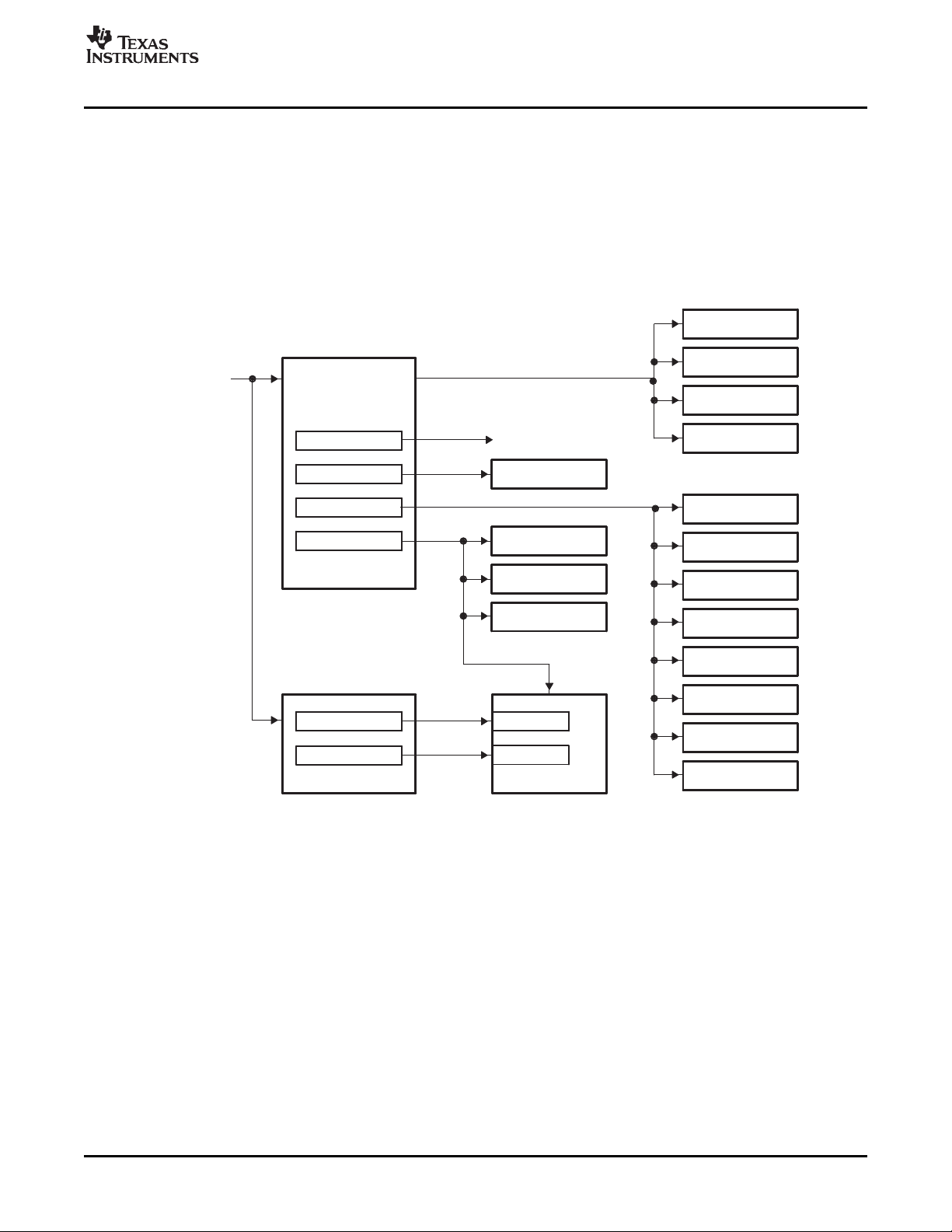
www.ti.com
DSP Subsystem
SYSCLK1
SYSCLK3
SCR
EDMA
DDR2 PHY
DDR2 VTP
DDR2 Mem Ctlr
PLLDIV1 (/2)
BPDIV
PLL Controller 2
PLL Controller 1
PLLDIV2 (/3)
PLLDIV3 (/6)
PLLDIV1 (/1)
SYSCLK2
UARTs (x2)
I2C
Timers (x3)
PWMs (x3)
EMAC
EMIFA
VLYNQ
HPI
McASP0
McBSP0
GPIO
McBSP1
PCI
MXI/CLKIN
(15−30 MHz)
OSCDIV1 (/1)
OBSCLK
(CLKOUT0 Pin)
AUXCLK
Device Clocking
Modules in the CLKDIV6 domain (for example, CLKDIV6 domain peripherals) must run at 1/6 the DSP
frequency.
Modules in the CLKIN domain (for example, UART, Timer, I2C, PWM) run at the MXI/CLKIN frequency,
asynchronous to the DSP. There is no fixed ratio requirement between these peripherals frequencies and
the DSP frequency.
Refer to device-specific data manual for the core clock domain for each peripheral.
Figure 1. Overall Clocking Diagram
SPRUES0B – December 2007 Phase-Locked Loop Controller (PLLC) 7
Submit Documentation Feedback
Page 8
www.ti.com
Device Clocking
1.2.2 Core Frequency Flexibility
The core frequency domain clocks are supplied by the PLL controller 1 (PLLC1). These domain clocks are
flexible, to a degree, within the limitations specified in the device-specific data manual. All of the following
frequency ranges and multiplier/divider ratios in the data manual must be adhered to:
• Input clock frequency range (MXI/CLKIN)
• PLL1 multiplier (PLLM) range
• PLL1 output (PLLOUT) frequency range based on the core voltage (1.05V or 1.2V) of the device
• Maximum device speed
• PLLC1's SYSCLK3:SYSCLK2:SYSCLK1 frequency ratio must be fixed to 1:3:6. For example, if
SYSCLK1 is at 600 MHZ, SYSCLK2 must be at 200 MHZ, and SYSCLK3 must be at 100 MHZ.
As specified in the data manual, the PLLs can be driven by any input ranging from 15 to 30 MHZ.
Table 2 shows some example PLL1 multiplier and divider settings assuming MXI/CLKIN frequency of 25
MHZ. The Applicable to Device Core Voltage column indicates whether the setting is allowed for a given
device core voltage. For example, the last row in Table 2 (PLL1 multiplier 24 for a 25 MHZ clock input)
only applies to devices with a core voltage 1.2V to meet the PLL1 output (PLLOUT) frequency range
required in the data manual. In addition, you must ensure the SYSCLK1 frequency does not exceed the
speed grade of the device. For example, for a device rated at 400 MHZ speed grade, SYSCLK1 must not
exceed 400 MHZ.
PLL1 PLLOUT Freq Freq Freq
Multiplier Freq (MHZ) Divider
16 400.0 1 400.0 3 133.3 6 66.7 Y Y
17 425.0 1 425.0 3 141.7 6 70.8 Y Y
18 450.0 1 450.0 3 150.0 6 75.0 Y Y
19 475.0 1 475.0 3 158.3 6 79.2 Y Y
20 500.0 1 500.0 3 166.7 6 83.3 Y Y
21 525.0 1 525.0 3 175.0 6 87.5 Y 22 550.0 1 550.0 3 183.3 6 91.7 Y 23 575.0 1 575.0 3 191.7 6 95.8 Y 24 600.0 1 600.0 3 200.0 6 100.0 Y
24 600.0 2 300.0 6 100.0 12 50.0 Y -
Table 2. Example PLL1 Frequencies and Dividers (25 MHZ Clock Input)
CLKDIV1 Domain CLKDIV3 Domain CLKDIV6 Domain Applicable to Device
(SYSCLK1) (SYSCLK2) (SYSCLK3) Core Voltage
PLL1
(1)
(MHZ) Divider
(1)
(MHZ) Divider
(1)
(MHZ) 1.2V 1.05V
(1)
The RATIO bit in PLLDIV n is programmed as Divider - 1. For example, for a SYSCLK1 divider of 1, you should program
PLLDIV1.RATIO = 0, PLLDIV2.RATIO = 2, PLLDIV3.RATIO = 5.
8 Phase-Locked Loop Controller (PLLC) SPRUES0B – December 2007
Submit Documentation Feedback
Page 9
www.ti.com
1.2.3 DDR2/EMIF Clock
The DDR2 interface has a dedicated clock driven from PLL2. This is a separate clock system from the
PLL1 clocks provided to other components of the system. This dedicated clock allows the reduction of the
core clock rates to save power while maintaining the required minimum clock rate (125 MHZ) for DDR2.
PLL2 must be configured to output a 2 × clock to the DDR2 PHY interface.
All of the following frequency ranges and multiplier/divider ratios in the device-specific data manual must
be adhered to when configuring PLL2:
• Input clock frequency range (MXI/CLKIN)
• PLL2 multiplier (PLLM) range
• PLL2 output (PLLOUT) frequency range based on core voltage (1.05V or 1.2V) of the device
Table 3 and Table 4 show some PLL2/DDR2 clock rates assuming a MXI/CLKIN frequency of 25 MHZ.
PLL2 Multiplier (MHZ) Divider
Table 3. Example PLL2 Frequencies (Core Voltage = 1.2V)
PLL2 PLLOUT Freq SYSCLK1
20 500.0 2 250.0 125.0
21 525.0 2 262.5 131.3
22 550.0 2 275.0 137.5
23 575.0 2 287.5 143.8
24 600.0 2 300.0 150.0
25 625.0 2 312.5 156.3
26 650.0 2 325.0 162.5
30 750.0 3 250.0 125.0
31 775.0 3 258.3 129.2
32 800.0 3 266.7 133.3
(1)
PHY [2 × clock] (MHZ) DDR2 Clock (MHZ)
Device Clocking
(1)
The RATIO bit in PLLDIV n is programmed as Divider - 1. For example, for SYSCLK1 divider of 3, you should program
PLLDIV1.RATIO = 2.
Table 4. Example PLL2 Frequencies (Core Voltage = 1.05V)
PLL2 Multiplier (MHZ) Divider
20 500.0 2 250.0 125.0
21 525.0 2 262.5 131.3
22 550.0 2 275.0 137.5
23 575.0 2 287.5 143.8
24 600.0 2 300.0 150.0
25 625.0 2 312.5 156.3
26 650.0 2 325.0 162.5
(1)
The RATIO bit in PLLDIV n is programmed as Divider - 1. For example, for SYSCLK1 divider of 3, you should program
PLLDIV1.RATIO = 2.
PLL2 PLLOUT Freq SYSCLK1
(1)
PHY [2 × clock] (MHZ) DDR2 Clock (MHZ)
SPRUES0B – December 2007 Phase-Locked Loop Controller (PLLC) 9
Submit Documentation Feedback
Page 10
www.ti.com
Device Clocking
1.2.4 I/O Domains
The I/O domains refer to the frequencies of the peripherals that communicate through device pins. In
many cases, there are frequency requirements for a peripheral pin interface that are set by an outside
standard and must be met. It is not necessarily possible to obtain these frequencies from the on-chip clock
generation circuitry, so the frequencies must be obtained from external sources and are asynchronous to
the core frequency domain by definition.
Table 5 lists peripherals with external I/O interface, and their I/O domain clock/frequency. It also shows the
core clock domain as a reference to show the core clock used for internal communications. See section
Section 1.2.1 for more details on core clock domains. See device-specific data manual for the exact I/O
clock frequency supported on the device.
Table 5. Peripheral I/O Domain Clock
Peripheral Frequency Internal Clock Source External Clock Source Core Clock Domain
I/O Domain Clock
DDR2 125-166 MHZ PLLC2 SYSCLK1 — CLKDIV3
PCI 33 MHZ — PCICLK CLKDIV3
EMAC (MII) 25 MHZ — MTXCLK, MRXCLK CLKDIV6
EMAC (RMII) 50 MHZ — RMREFCLK CLKDIV6
VLYNQ up to 80 MHZ PLLC1 SYSCLK3 VLYNQ_CLOCK CLKDIV6
McBSP up to 40 MHZ PLLC1 SYSCLK3 CLKS, CLKX, CLKR CLKDIV6
McASP up to 40 MHZ PLLC1 SYSCLK3 AHCLKX, AHCLKR, CLKDIV6
GPIO NA (asynchronous — — CLKDIV6
interface)
EMIFA NA (asynchronous — — CLKDIV6
interface)
HPI NA (asynchronous — — CLKDIV6
interface)
I2C up to 400 kHz MXI/CLKIN SCL CLKIN
Timer output up to 1/2 CLKIN MXI/CLKIN TINP0L (Timer 0), CLKIN
frequency TINP1L (Timer 1)
input up to 1/4 CLKIN
frequency
Watchdog Timer NA MXI/CLKIN — CLKIN
PWM NA — — CLKIN
UART NA — — CLKIN
I/O (External) Domain Clock Source Options
ACLKX, ACLKR
10 Phase-Locked Loop Controller (PLLC) SPRUES0B – December 2007
Submit Documentation Feedback
Page 11

www.ti.com
2 PLL Controller
2.1 PLL Module
PLL Controller
The C642x DSP has two PLLs (PLL1 and PLL2) that provide clocks to different parts of the system. PLL1
provides clocks (though various dividers) to most of the components of the C642x DSP. PLL2 is dedicated
to the DDR2 port. The reference clock is the 15 to 30 MHZ crystal or 1.8V LVCMOS-compatible clock
input, as mentioned in the data manual.
The PLL controller provides the following:
• Glitch-Free Transitions (on changing clock settings)
• Domain Clocks Alignment
• Clock Gating
• PLL power down
The various clock outputs given by the controller are as follows:
• Domain Clocks: SYSCLK[1: n]
• Auxiliary Clock from reference clock source: AUXCLK
• Bypass Domain clock: SYSCLKBP
• Observe Clock: OBSCLK
Various dividers that can be used on the C642x DSP are as follows:
• PLL Controller Dividers (for SYSCLK[1: n]): PLLDIV1, ..., PLLDIV n
• Bypass Divider (for SYSCLKBP): BPDIV
• Oscillator Divider (for OBSCLK): OSCDIV1
Various other controls supported are as follows:
• PLL Multiplier Control: PLLM
• Software-programmable PLL Bypass: PLLEN
SPRUES0B – December 2007 Phase-Locked Loop Controller (PLLC) 11
Submit Documentation Feedback
Page 12

www.ti.com
PLLDIV1(/1)
PLLDIV3(/6)
PLLDIV2(/3)
SYSCLK1
(CLKDIV1Domain)
SYSCLK3
(CLKDIV6Domain)
SYSCLK2
(CLKDIV3Domain)
1
0
PLLM
PLL
0
1
CLKMODE
CLKIN
OSCIN
PLLEN
AUXCLK
(CLKINDomain)
OSCDIV1
OBSCLK
(CLKOUT0Pin)
PLLOUT
PLL Controller
2.2 PLL1 Control
PLL1 supplies the primary C642x DSP system clock. Software controls the PLL1 operation through the
system PLL controller 1 (PLLC1) registers. The registers used in PLLC1 are listed in Section 2.4 . Figure 2
shows the customization of PLL1 in the C642x DSP. The domain clocks are distributed to the core clock
domains (discussed in Section 1.2.1 ) and the rest of the device as follows:
• SYSCLK1: CLKDIV1 Domain
• SYSCLK2: CLKDIV3 Domain
• SYSCLK3: CLKDIV6 Domain
• AUXCLK: CLKIN Domain
• OBSCLK: CLKOUT0 pin
The PLL1 multiplier is controlled by the PLLM bit of the PLL multiplier control register (PLLM). The PLL1
output clock may be divided-down for slower device operation using the PLLC1 SYSCLK dividers
PLLDIV1, PLLDIV2, and PLLDIV3.
You are responsible to adhere to the PLLC1 frequency ranges and multiplier/divider ratios specified in the
data manual. See also Section 1.2.1 and Section 1.2.2 .
At power-up, PLL1 is powered-down and disabled, and must be powered-up by software through the PLL1
PLLPWRDN bit in the PLL control register (PLLCTL). By default, the system operates in bypass mode and
the system clock is provided directly from the input reference clock (MXI/CLKIN pin). Once the PLL is
powered-up and locked, software can switch the device to PLL mode operation by setting the PLLEN bit in
PLLCTL to 1. If the boot mode of the device is set to fast boot (FASTBOOT = 1), the bootloader code in
the Boot ROM will follow the previous process to power-up and lock the PLL, and switch the device to PLL
mode to speed up the boot process. Therefore, coming out of a fast boot, the device is operating in PLL
mode.
Figure 2. PLL1 Structure in the TMS320C642x DSP
12 Phase-Locked Loop Controller (PLLC) SPRUES0B – December 2007
Submit Documentation Feedback
Page 13

www.ti.com
2.2.1 Device Clock Generation
PLLC1 generates several clocks from the PLL1 output clock for use by the various processors and
modules. These are summarized in Table 6 . SYSCLK1, SYSCLK2, and SYSCLK3 must maintain a fixed
frequency ratio requirement, no matter what reference clock (PLL or bypass) or PLL frequency is used.
PLLC1 Output Clock Used by Default Divider
SYSCLK1 DSP /1
SYSCLK2 SCR, EDMA, CLKDIV3 Domain peripherals /3
SYSCLK3 CLKDIV6 Domain peripherals /6
AUXCLK CLKIN Domain peripherals NA
OBSCLK CLKOUT0 source /1
2.2.2 Steps for Changing PLL1/Core Domain Frequency
Refer to the appropriate subsection on how to program the PLL1/Core Domain clocks:
• If the PLL is powered down (PLLPWRDN bit in PLLCTL is set to 1), follow the full PLL initialization
procedure in Section 2.2.2.1 to initialize the PLL.
• If the PLL is not powered down (PLLPWRDN bit in PLLCTL is cleared to 0), follow the sequence in
Section 2.2.2.2 to change the PLL multiplier.
• If the PLL is already running at a desired multiplier and you only want to change the SYSCLK dividers,
follow the sequence in Section 2.2.2.3 .
Note that the PLL is powered down after the following device-level global resets:
• Power-on Reset ( POR)
• Warm Reset ( RESET)
• Max Reset
PLL Controller
Table 6. System PLLC1 Output Clocks
2.2.2.1 Initialization to PLL Mode from PLL Power Down
If the PLL is powered down (PLLPWRDN bit in PLLCTL is set to 1), you must follow the procedure below
to change PLL1 frequencies. The recommendation is to stop all peripheral operation before changing the
PLL1 frequency, with the exception of the C64x+ DSP and DDR2. The C64x+ DSP must be operational to
program the PLL controller. DDR2 operates off of the clock from PLLC2.
1. Select the clock mode by programming the CLKMODE bit in PLLCTL.
2. Before changing the PLL frequency, switch to PLL bypass mode:
a. Clear the PLLENSRC bit in PLLCTL to 0 to allow PLLCTL.PLLEN to take effect.
b. Clear the PLLEN bit in PLLCTL to 0 (select PLL bypass mode).
c. Wait for 4 MXI cycles to ensure PLLC switches to bypass mode properly.
3. Clear the PLLRST bit in PLLCTL to 0 (reset PLL)
4. Set the PLLDIS bit in PLLCTL to 1 (disable PLL output).
5. Clear the PLLPWRDN bit in PLLCTL to 0 to bring the PLL out of power-down mode.
6. Clear the PLLDIS bit in PLLCTL to 0 (enable the PLL) to allow PLL outputs to start toggling. Note that
the PLLC is still at PLL bypass mode; therefore, the toggling PLL output does not get propagated to
the rest of the device.
7. Wait for PLL stabilization time. See the device-specific data manual for PLL stabilization time.
8. Program the required multiplier value in PLLM.
SPRUES0B – December 2007 Phase-Locked Loop Controller (PLLC) 13
Submit Documentation Feedback
Page 14

www.ti.com
PLL Controller
9. If necessary, program PLLDIV1, PLLDIV2, and PLLDIV3 registers to change the SYSCLK1, SYSCLK2,
and SYSCLK3 divide values:
a. Check for the GOSTAT bit in PLLSTAT to clear to 0 to indicate that no GO operation is currently in
progress.
b. Program the RATIO field in PLLDIV1, PLLDIV2, and PLLDIV3 with the desired divide factors. Note
that the dividers must maintain a 1:3:6 ratio to satisfy the CLKDIV1, CLKDIV3, CLKDIV6 clock
domain requirements. See the device-specific data manual for more details on Clock Domains. In
addition, in this step make sure you leave the PLLDIV1.D1EN, PLLDIV2.D2EN, and
PLLDIV3.D3EN bits set (default).
c. Set the GOSET bit in PLLCMD to 1 to initiate a new divider transition. During this transition,
SYSCLK1, SYSCLK2, and SYSCLK3 are paused momentarily.
d. Wait for N number of PLLDIV n source clock cycles to ensure divider changes have completed. See
Section 2.2.2.3 for the formula on calculating the number of cycles N.
e. Wait for the GOSTAT bit in PLLSTAT to clear to 0.
10. Wait for PLL to reset properly. See the device-specific data manual for PLL reset time.
11. Set the PLLRST bit in PLLCTL to 1 to bring the PLL out of reset.
12. Wait for PLL to lock. See the device-specific data manual for PLL lock time.
13. Set the PLLEN bit in PLLCTL to 1 to remove the PLL from bypass mode.
2.2.2.2 Changing PLL Multiplier
If the PLL is not powered down (PLLPWRDN bit in PLLCTL is cleared to 0) and the PLL stabilization time
is previously met (step 7 in Section 2.2.2.1 ), follow this procedure to change PLL1 multiplier. The
recommendation is to stop all peripheral operation before changing the PLL multiplier, with the exception
of the C64x+ DSP and DDR2. The C64x+ DSP must be operational to program the PLL controller. DDR2
operates off of the clock from PLLC2.
1. Before changing the PLL frequency, switch to PLL bypass mode:
a. Clear the PLLENSRC bit in PLLCTL to 0 to allow PLLCTL.PLLEN to take effect.
b. Clear the PLLEN bit in PLLCTL to 0 (select PLL bypass mode).
c. Wait for 4 MXI cycles to ensure PLLC switches to bypass mode properly.
2. Clear the PLLRST bit in PLLCTL to 0 (reset PLL).
3. Clear the PLLDIS bit in PLLCTL to 0 (enable the PLL) to allow PLL outputs to start toggling. Note that
the PLLC is still at PLL bypass mode; therefore, the toggling PLL output does not get propagated to
the rest of the device.
4. Program the required multiplier value in PLLM.
5. If necessary, program PLLDIV1, PLLDIV2, and PLLDIV3 registers to change the SYSCLK1, SYSCLK2,
and SYSCLK3 divide values:
a. Check for the GOSTAT bit in PLLSTAT to clear to 0 to indicate that no GO operation is currently in
progress.
b. Program the RATIO field in PLLDIV1, PLLDIV2, and PLLDIV3 with the desired divide factors. Note
that the dividers must maintain a 1:3:6 ratio to satisfy the CLKDIV1, CLKDIV3, CLKDIV6 clock
domain requirements. See the device-specific data manual for more details on Clock Domains. In
addition, in this step make sure you leave the PLLDIV1.D1EN, PLLDIV2.D2EN, and
PLLDIV3.D3EN bits set (default).
c. Set the GOSET bit in PLLCMD to 1 to initiate a new divider transition. During this transition,
SYSCLK1, SYSCLK2, and SYSCLK3 are paused momentarily.
d. Wait for N number of PLLDIV n source clock cycles to ensure divider changes have completed. See
Section 2.2.2.3 for the formula on calculating the number of cycles N.
e. Wait for the GOSTAT bit in PLLSTAT to clear to 0.
6. Wait for PLL to reset properly. See the device-specific data manual for PLL reset time.
7. Set the PLLRST bit in PLLCTL to 1 to bring the PLL out of reset.
8. Wait for PLL to lock. See the device-specific data manual for PLL lock time.
9. Set the PLLEN bit in PLLCTL to 1 to remove the PLL from bypass mode.
Phase-Locked Loop Controller (PLLC)14 SPRUES0B – December 2007
Submit Documentation Feedback
Page 15

www.ti.com
2.2.2.3 Changing SYSCLK Dividers
This section discusses the software sequence to change the SYSCLK dividers. The SYSCLK divider
change sequence is also referred to as GO operation, as it involves hitting the GO bit (GOSET bit in
PLLCMD) to initiate the divider change. The recommendation is to stop all peripheral operation before
changing the SYSCLK dividers, with the exception of the C64x+ DSP and DDR2. The C64x+ DSP must
be operational to program the PLL controller. DDR2 operates off of the clock from PLLC2.
1. Check for the GOSTAT bit in PLLSTAT to clear to 0 to indicate that no GO operation is currently in
progress.
2. Program the RATIO field in PLLDIV1, PLLDIV2, and PLLDIV3 with the desired divide factors. Note that
the dividers must maintain a 1:3:6 ratio to satisfy the CLKDIV1, CLKDIV3, CLKDIV6 clock domain
requirements. See the device-specific data manual for more details on Clock Domains. In addition, in
this step make sure you leave the PLLDIV1.D1EN, PLLDIV2.D2EN, and PLLDIV3.D3EN bits set
(default).
3. Set the GOSET bit in PLLCMD to 1 to initiate a new divider transition. During this transition, SYSCLK1,
SYSCLK2, and SYSCLK3 are paused momentarily.
4. Wait for N number of PLLDIV n source clock cycles to ensure divider changes have completed. See the
following formula for calculating the number of cycles N.
5. Wait for the GOSTAT bit in PLLSTAT to clear to 0.
The following formula should be used to calculate the number of PLLDIV n source clock cycles:
N = (2 × Least Common Multiple [LCM] of all the old SYSCLK divide values) + 50 cycles overhead
Example 1. Calculating Number of Clock Cycles N
PLL Controller
This example calculates the number of clock cycles N.
• Settings before divider change:
– PLLDIV1.RATIO = 0 (divide-by-1)
– PLLDIV2.RATIO = 2 (divide-by-3)
– PLLDIV3.RATIO = 5 (divide-by-6)
• New divider settings:
– PLLDIV1.RATIO = 1 (divide-by-2)
– PLLDIV2.RATIO = 5 (divide-by-6)
– PLLDIV3.RATIO = 11 (divide-by-12)
The least common multiple between the old divider values of /1, /3, and /6 is /6; therefore, the number
of cycles N is:
N = (2 × 6) + 50 cycles overhead = 62 PLLDIV n source clock cycles
If PLLC1 is in PLL mode (PLLCTL.PLLEN = 1), the PLLDIV n source clock is the PLL1 output clock. If
PLLC1 is in PLL bypass mode (PLLCTL.PLLEN = 0), the PLLDIV n source clock is the device clock
source MXI/CLKIN.
SPRUES0B – December 2007 Phase-Locked Loop Controller (PLLC) 15
Submit Documentation Feedback
Page 16

www.ti.com
PLLDIV1 (/2)
1
0
PLLM
PLL
0
1
BPDIV
CLKMODE
CLKIN
OSCIN
PLLEN
PLL2_SYSCLK1
(DDR2 PHY)
PLL2_SYSCLKBP
(DDR2 VTP)
PLLOUT
PLL Controller
2.3 PLL2 Control
PLL2 provides the clock from which the DDR2 memory controller clocks are derived. The DDR PLL
controller 2 (PLLC2) controls PLL2, which accepts the clock from the oscillator and also generates the
various frequency clocks needed. Figure 3 shows the customization of PLL2 in the C642x DSP. The PLL2
clocks are distributed to the device as follows:
• SYSCLK1: DDR2 PHY
• SYSCLKBP: DDR2 VTP
PLL2 supplies the DDR2 memory controller clock. Software controls the PLL2 operation through the DDR
PLL controller 2 (PLLC2) registers. The registers used in PLLC2 are listed in Section 2.4 . The PLL2
multiplier is controlled by the PLLM bit of the PLL multiplier control register (PLLM). The PLL2 multiplier
may be modified by software (for example, to tune the DDR interface for best performance).
The PLL2 output clock must be divided-down to the DDR operating range using the SYSCLK1 divider.
At power-up, PLL2 is powered-down and disabled, and must be powered-up by software through the PLL2
PLLPWRDN bit in the PLL control register (PLLCTL). By default, the system operates in bypass mode and
the DDR clock is provided directly from the input reference clock. Once the PLL is powered-up and locked,
software can switch the device to PLL mode operation by setting the PLLEN bit in PLLCTL to 1.
Figure 3. PLL2 Structure in the TMS320C642x DSP
16 Phase-Locked Loop Controller (PLLC) SPRUES0B – December 2007
Submit Documentation Feedback
Page 17

www.ti.com
2.3.1 Device Clock Generation
PLLC2 generates clocks from the PLL2 output clock for use by the DDR2 memory controller. These are
summarized in Table 7 .
Output Clock Used by Default Divider
SYSCLK1 DDR Phy /2
SYSCLKBP DDR VTP Controller /2
The SYSCLK1 output clock divider value defaults to /2. Assuming a 25 MHZ MXI/CLKIN and the PLL2
default multiplier of × 20, this results in a 250 MHZ DDR Phy clock (125 MHZ DDR2). It can be modified by
software (RATIO bit in PLLDIV1) in combination with other PLL multipliers to achieve the desired DDR
clock rate.
2.3.2 Steps for Changing PLL2 Frequency
The PLLC2 is programmed similarly to the PLLC1. Refer to the appropriate subsection on how to program
the PLL2 clocks:
• If the PLL is powered down (PLLPWRDN bit in PLLCTL is set to 1), follow the full PLL initialization
procedure in Section 2.3.2.2 to initialize the PLL.
• If the PLL is not powered down (PLLPWRDN bit in PLLCTL is cleared to 0), follow the sequence in
Section 2.3.2.3 to change the PLL multiplier.
• If the PLL is already running at a desired multiplier and you only want to change the SYSCLK dividers,
follow the sequence in Section 2.3.2.4 .
Note that the PLL is powered down after the following device-level global resets:
• Power-on Reset ( POR)
• Warm Reset ( RESET)
• Max Reset
PLL Controller
Table 7. DDR PLLC2 Output Clocks
In addition, note that the PLL2 frequency directly affects the DDR2 memory controller. The DDR2 memory
controller requires special sequences to be followed before and after you change the PLL2 frequency. You
must follow the additional considerations for the DDR2 memory controller in Section 2.3.2.1 in order to not
corrupt DDR2 operation.
2.3.2.1 DDR2 Considerations When Modifying PLL2 Frequency
Before changing PLL2 and/or PLLC2 frequency, you must take into account the DDR2 memory controller
requirements. If the DDR2 memory controller is used in the system, follow the additional steps in this
section to change PLL2 and/or PLLC2 frequency without corrupting DDR2 operation.
• If the DDR2 memory controller is in reset when you desire to change the PLL2 frequency, follow the
steps in Example 2 .
• If the DDR2 memory controller is already out of reset when you desire to change the PLL2 frequency,
follow the steps in Example 3 .
SPRUES0B – December 2007 Phase-Locked Loop Controller (PLLC) 17
Submit Documentation Feedback
Page 18

www.ti.com
PLL Controller
Example 2. PLL2 Frequency Change Steps When DDR2 Memory Controller is In Reset
This example discusses the steps to change the PLL2 frequency when the DDR2 memory controller is
in reset. Note that the DDR2 memory controller is in reset after these device-level global resets:
power-on reset, warm reset, max reset.
1. Leave the DDR2 memory controller in reset.
2. Program the PLL2 clocks by following the steps in the appropriate section: Section 2.3.2.2 ,
Section 2.3.2.3 , or Section 2.3.2.4 . (Discussion in Section 2.3.2 explains which is the appropriate
subsection).
3. Initialize the DDR2 memory controller. The steps for DDR2 memory controller initialization are found
in the TMS320C642x DSP DDR2 Memory Controller User's Guide (SPRUEM4 ).
Example 3. PLL2 Frequency Change Steps When DDR2 Memory Controller is Out of Reset
This example discusses the steps to change the PLL2 frequency when the DDR2 memory controller is
already out of reset.
1. Stop DDR2 memory controller accesses and purge any outstanding requests.
2. Put the DDR2 memory in self-refresh mode and stop the DDR2 memory controller clock. The DDR2
memory controller clock shut down sequence is in the TMS320C642x DSP DDR2 Memory
Controller User's Guide (SPRUEM4 ).
3. Program the PLL2 clocks by following the steps in the appropriate section: Section 2.3.2.2 ,
Section 2.3.2.3 , or Section 2.3.2.4 . (Discussion in Section 2.3.2 explains which is the appropriate
subsection).
4. Re-enable the DDR2 memory controller clock. The DDR2 memory controller clock on sequence is in
the TMS320C642x DSP DDR2 Memory Controller User's Guide (SPRUEM4 ).
2.3.2.2 Initialization to PLL Mode from PLL Power Down
If the PLL is powered down (PLLPWRDN bit in PLLCTL is set to 1), you must follow the procedure below
to change PLL2 frequencies.
1. Select the clock mode by programming the CLKMODE bit in PLLCTL.
2. Before changing the PLL frequency, switch to PLL bypass mode:
a. Clear the PLLENSRC bit in PLLCTL to 0 to allow PLLCTL.PLLEN to take effect.
b. Clear the PLLEN bit in PLLCTL to 0 (select PLL bypass mode).
c. Wait for 4 MXI cycles to ensure PLLC switches to bypass mode properly.
3. Clear the PLLRST bit in PLLCTL to 0 (reset PLL)
4. Set the PLLDIS bit in PLLCTL to 1 (disable PLL output).
5. Clear the PLLPWRDN bit in PLLCTL to 0 to bring the PLL out of power-down mode.
6. Clear the PLLDIS bit in PLLCTL to 0 (enable the PLL) to allow PLL outputs to start toggling. Note that
the PLLC is still at PLL bypass mode; therefore, the toggling PLL output does not get propagated to
the rest of the device.
7. Wait for PLL stabilization time. See the device-specific data manual for PLL stabilization time.
18 Phase-Locked Loop Controller (PLLC) SPRUES0B – December 2007
Submit Documentation Feedback
Page 19

www.ti.com
8. Program the required multiplier value in PLLM.
9. If necessary, program PLLDIV1 register to change the SYSCLK1 divide value:
a. Check for the GOSTAT bit in PLLSTAT to clear to 0 to indicate that no GO operation is currently in
progress.
b. Program the RATIO field in PLLDIV1 with the desired divide factor. In this step make sure you
leave the PLLDIV1.D1EN bit set (default).
c. Set the GOSET bit in PLLCMD to 1 to initiate a new divider transition. During this transition,
SYSCLK1 is paused momentarily.
d. Wait for N number of PLLDIV n source clock cycles to ensure divider changes have completed. See
Section 2.3.2.4 for the formula on calculating the number of cycles N.
e. Wait for the GOSTAT bit in PLLSTAT to clear to 0.
10. Wait for PLL to reset properly. See the device-specific data manual for PLL reset time.
11. Set the PLLRST bit in PLLCTL to 1 to bring the PLL out of reset.
12. Wait for PLL to lock. See the device-specific data manual for PLL lock time.
13. Set the PLLEN bit in PLLCTL to 1 to remove the PLL from bypass mode.
For information on initializing the DDR2 memory controller, see the TMS320C642x DSP DDR2 Memory
Controller User's Guide (SPRUEM4 ).
2.3.2.3 Changing PLL Multiplier
If the PLL is not powered down (PLLPWRDN bit in PLLCTL is cleared to 0) and the PLL stabilization time
is previously met (step 7 in Section 2.3.2.2 ), follow this procedure to change PLL2 multiplier.
1. Before changing the PLL frequency, switch to PLL bypass mode:
a. Clear the PLLENSRC bit in PLLCTL to 0 to allow PLLCTL.PLLEN to take effect.
b. Clear the PLLEN bit in PLLCTL to 0 (select PLL bypass mode).
c. Wait for 4 MXI cycles to ensure PLLC switches to bypass mode properly.
2. Clear the PLLRST bit in PLLCTL to 0 (reset PLL).
3. Clear the PLLDIS bit in PLLCTL to 0 (enable the PLL) to allow PLL outputs to start toggling. Note that
the PLLC is still at PLL bypass mode; therefore, the toggling PLL output does not get propagated to
the rest of the device.
4. Program the required multiplier value in PLLM.
5. If necessary, program PLLDIV1 register to change the SYSCLK1 divide value:
a. Check for the GOSTAT bit in PLLSTAT to clear to 0 to indicate that no GO operation is currently in
progress.
b. Program the RATIO field in PLLDIV1 with the desired divide factor. In this step make sure you
leave the PLLDIV1.D1EN bit set (default).
c. Set the GOSET bit in PLLCMD to 1 to initiate a new divider transition. During this transition,
SYSCLK1 is paused momentarily.
d. Wait for N number of PLLDIV n source clock cycles to ensure divider changes have completed. See
Section 2.3.2.4 for the formula on calculating the number of cycles N.
e. Wait for the GOSTAT bit in PLLSTAT to clear to 0.
6. Wait for PLL to reset properly. See the device-specific data manual for PLL reset time.
7. Set the PLLRST bit in PLLCTL to 1 to bring the PLL out of reset.
8. Wait for PLL to lock. See the device-specific data manual for PLL lock time.
9. Set the PLLEN bit in PLLCTL to 1 to remove the PLL from bypass mode.
PLL Controller
SPRUES0B – December 2007 Phase-Locked Loop Controller (PLLC) 19
Submit Documentation Feedback
Page 20

www.ti.com
PLL Controller
2.3.2.4 Changing SYSCLK Dividers
This section discusses the software sequence to change the SYSCLK dividers. The SYSCLK divider
change sequence is also referred to as GO operation, as it involves hitting the GO bit (GOSET bit in
PLLCMD) to initiate the divider change.
1. Check for the GOSTAT bit in PLLSTAT to clear to 0 to indicate that no GO operation is currently in
progress.
2. Program the RATIO field in PLLDIV1 with the desired divide factor. In this step make sure you leave
the PLLDIV1.D1EN bit set (default).
3. Set the GOSET bit in PLLCMD to 1 to initiate a new divider transition. During this transition, SYSCLK1
is paused momentarily.
4. Wait for N number of PLLDIV n source clock cycles to ensure divider changes have completed. See the
following formula for calculating the number of cycles N.
5. Wait for the GOSTAT bit in PLLSTAT to clear to 0.
The following formula should be used to calculate the number of PLLDIV n source clock cycles:
N = (2 × old SYSCLK1 divide value) + 50 cycles overhead
Example 4. Calculating Number of Clock Cycles N
This example calculates the number of clock cycles N.
• Settings before divider change:
– PLLDIV1.RATIO = 1 (divide-by-2)
• New divider settings:
– PLLDIV1.RATIO = 2 (divide-by-3)
Therefore, the number of cycles N is:
N = (2 × 2) + 50 cycles overhead = 54 PLLDIV n source clock cycles
If PLLC2 is in PLL mode (PLLCTL.PLLEN = 1), the PLLDIV n source clock is the PLL2 output clock. If
PLLC2 is in PLL bypass mode (PLLCTL.PLLEN = 0), the PLLDIV n source clock is the device clock
source MXI/CLKIN.
20 Phase-Locked Loop Controller (PLLC) SPRUES0B – December 2007
Submit Documentation Feedback
Page 21

www.ti.com
2.4 PLL Controller Registers
Table 8 lists the base address and end address for the PLL controllers. Table 9 lists the memory-mapped
registers for the PLL and reset controller. See the device-specific data manual for the memory address of
these registers.
Offset Acronym Register Description Section
00h PID Peripheral ID Register Section 2.4.1
E4h RSTYPE
100h PLLCTL PLL Control Register Section 2.4.3
110h PLLM PLL Multiplier Control Register Section 2.4.4
118h PLLDIV1 PLL Controller Divider 1 Register (SYSCLK1) Section 2.4.5
11Ch PLLDIV2
120h PLLDIV3
124h OSCDIV1
12Ch BPDIV
138h PLLCMD PLL Controller Command Register Section 2.4.10
13Ch PLLSTAT PLL Controller Status Register Section 2.4.11
140h ALNCTL PLL Controller Clock Align Control Register Section 2.4.12
144h DCHANGE PLLDIV Ratio Change Status Register Section 2.4.13
148h CKEN
14Ch CKSTAT Clock Status Register Section 2.4.15
150h SYSTAT SYSCLK Status Register Section 2.4.16
Table 8. PLL and Reset Controller List
PLL and Reset Controller Base Address End Address Size
PLLC1 1C4 0800h 1C4 0BFFh 400h
PLLC2 1C4 0C00h 1C4 0FFFh 400h
Table 9. PLL and Reset Controller Registers
(1)
(1)
(1)
(1)
(2)
(1)
Reset Type Status Register Section 2.4.2
PLL Controller Divider 2 Register (SYSCLK2) Section 2.4.6
PLL Controller Divider 3 Register (SYSCLK3) Section 2.4.7
Oscillator Divider 1 Register (OBSCLK) Section 2.4.8
Bypass Divider Register Section 2.4.9
Clock Enable Control Register Section 2.4.14
PLL Controller
(1)
not supported for PLL2.
(2)
not supported for PLL1.
SPRUES0B – December 2007 Phase-Locked Loop Controller (PLLC) 21
Submit Documentation Feedback
Page 22

www.ti.com
PLL Controller
2.4.1 Peripheral ID Register (PID)
The peripheral ID register (PID) is shown in Figure 4 and described in Table 10 .
Figure 4. Peripheral ID Register (PID)
31 24 23 16
Reserved TYPE
R-0 R-1h
15 8 7 0
CLASS REV
R-8h R-Dh
LEGEND: R = Read only; - n = value after reset
Table 10. Peripheral ID Register (PID) Field Descriptions
Bit Field Value Description
31-24 Reserved 0 Reserved
23-16 TYPE Peripheral type
1h PLLC
15-8 CLASS Peripheral class
8h Current class
7-0 REV Peripheral revision
Dh Current revision
2.4.2 Reset Type Status Register (RSTYPE)
The reset type status register (RSTYPE) is shown in Figure 5 and described in Table 11 . It latches cause
of the last reset. Although the reset value of all bits is 0 after coming out of reset, one bit is set to 1 to
indicate the cause of the reset.
Figure 5. Reset Type Status Register (RSTYPE)
31 16
Reserved
R-0
15 3 2 1 0
Reserved MRST XWRST POR
R-0 R-0 R-0 R-0
LEGEND: R = Read only; - n = value after reset
Table 11. Reset Type Status Register (RSTYPE) Field Descriptions
Bit Field Value Description
31-3 Reserved 0 Reserved
2 MRST 0-1 Maximum reset. If 1, maximum reset was the reset to occur that is of highest priority.
1 XWRST 0-1 External warm reset. If 1, warm reset ( RESET) was the last reset to occur that is of highest priority.
0 POR 0-1 Power on reset. If 1, power on reset ( POR) was the last reset to occur that is of highest priority.
Phase-Locked Loop Controller (PLLC)22 SPRUES0B – December 2007
Submit Documentation Feedback
Page 23

www.ti.com
PLL Controller
2.4.3 PLL Control Register (PLLCTL)
The PLL control register (PLLCTL) is shown in Figure 6 and described in Table 12 .
Figure 6. PLL Control Register (PLLCTL)
31 16
Reserved
R-0
15 9 8 7 6 5 4 3 2 1 0
Reserved CLKMODE Reserved PLLENSRC PLLDIS PLLRST Rsvd PLLPWRDN PLLEN
R-0 R/W-0 R-1h R/W-1 R/W-1 R/W-0 R-0 R/W-1 R/W-0
LEGEND: R/W = Read/Write; R = Read only; - n = value after reset
Table 12. PLL Control Register (PLLCTL) Field Descriptions
Bit Field Value Description
31-9 Reserved 0 Reserved
8 CLKMODE Reference clock selection
0 Internal oscillator. If the device reference clock source is a crystal at MXI/CLKIN pin, the internal
oscillator must be selected as the clock source.
1 CLKIN square wave. This mode applies if the device reference clock source is a square wave at
MXI/CLKIN pin. When this mode is selected, the PLLC turns off the internal oscillator's bias resistor
to save power.
7-6 Reserved 1 Reserved
5 PLLENSRC 0 This bit must be cleared to 0 before PLLEN will have any effect.
4 PLLDIS Asserts DISABLE to PLL.
0 PLL disable is de-asserted.
1 PLL disable is asserted. PLL output is disabled and not toggling.
3 PLLRST Asserts RESET to PLL if supported.
0 PLL reset is asserted. See device-specific data manual for the PLL reset time required.
1 PLL reset is not asserted.
2 Reserved 0 Reserved
1 PLLPWRDN PLL power-down. After powering up the PLL (PLLPWRDN 1 to 0 transition), you must wait for the
0 PLLEN PLL mode enable.
PLL to stabilize. See device-specific data manual for the PLL stabilization time.
0 PLL operational.
1 PLL power-down.
0 Bypass mode
1 PLL mode, not bypassed
SPRUES0B – December 2007 Phase-Locked Loop Controller (PLLC) 23
Submit Documentation Feedback
Page 24

www.ti.com
PLL Controller
2.4.4 PLL Multiplier Control Register (PLLM)
The PLL multiplier control register (PLLM) is shown in Figure 7 and described in Table 13 .
Figure 7. PLL Multiplier Control Register (PLLM)
31 16
Reserved
R-0
15 5 4 0
Reserved PLLM
R-0 R/W-10h or 13h
LEGEND: R/W = Read/Write; R = Read only; - n = value after reset
(1)
For PLLC1, PLLM defaults to 10h (PLL multiply by 17); For PLLC2, PLLM defaults to 13h (PLL multiply by 20).
(1)
Table 13. PLL Multiplier Control Register (PLLM) Field Descriptions
Bit Field Value Description
31-5 Reserved 0 Reserved
4-0 PLLM 0-1Fh PLL multiplier select. Multiplier value = PLLM + 1. For example, PLLM = 16 (10h) means multiply by 17.
See device-specific data manual for valid multiplier values for each PLL.
2.4.5 PLL Controller Divider 1 Register (PLLDIV1)
The PLL controller divider 1 register (PLLDIV1) is shown in Figure 8 and described in Table 14 . Divider 1
controls divider for SYSCLK1.
Figure 8. PLL Controller Divider 1 Register (PLLDIV1)
31 16
Reserved
R-0
15 14 5 4 0
D1EN Reserved RATIO
R/W-0 R-0 R/W-0 or 1
LEGEND: R/W = Read/Write; R = Read only; - n = value after reset
(1)
For PLLC1, RATIO defaults to 0 (PLL1 divide by 1); for PLLC2, RATIO defaults to 1 (PLL2 divide by 2).
(1)
Table 14. PLL Controller Divider 1 Register (PLLDIV1) Field Descriptions
Bit Field Value Description
31-16 Reserved 0 Reserved
15 D1EN Divider 1 enable.
0 Divider 1 is disabled.
1 Divider 1 is enabled.
14-5 Reserved 0 Reserved
4-0 RATIO 0-1Fh Divider ratio. Divider value = RATIO + 1. For example, RATIO = 0 means divide by 1.
24 Phase-Locked Loop Controller (PLLC) SPRUES0B – December 2007
Submit Documentation Feedback
Page 25

www.ti.com
PLL Controller
2.4.6 PLL Controller Divider 2 Register (PLLDIV2)
The PLL controller divider 2 register (PLLDIV2) is shown in Figure 9 and described in Table 15 . Divider 2
controls divider for SYSCLK2. PLLDIV2 is not used on PLLC2.
Figure 9. PLL Controller Divider 2 Register (PLLDIV2)
31 16
Reserved
R-0
15 14 5 4 0
D2EN Reserved RATIO
R/W-1 R-0 R/W-2h
LEGEND: R/W = Read/Write; R = Read only; - n = value after reset
Table 15. PLL Controller Divider 2 Register (PLLDIV2) Field Descriptions
Bit Field Value Description
31-16 Reserved 0 Reserved
15 D2EN Divider 2 enable.
0 Divider 2 is disabled.
1 Divider 2 is enabled.
14-5 Reserved 0 Reserved
4-0 RATIO 0-1Fh Divider ratio. Divider value = RATIO + 1. For example, RATIO = 0 means divide by 1.
2.4.7 PLL Controller Divider 3 Register (PLLDIV3)
The PLL controller divider 3 register (PLLDIV3) is shown in Figure 10 and described in Table 16 . Divider 3
controls divider for SYSCLK3. PLLDIV3 is not used on PLLC2.
Figure 10. PLL Controller Divider 3 Register (PLLDIV3)
31 16
Reserved
R-0
15 14 5 4 0
D3EN Reserved RATIO
R/W-1 R-0 R/W-5h
LEGEND: R/W = Read/Write; R = Read only; - n = value after reset
Table 16. PLL Controller Divider 3 Register (PLLDIV3) Field Descriptions
Bit Field Value Description
31-16 Reserved 0 Reserved
15 D3EN Divider 3 enable.
0 Divider 3 is disabled.
1 Divider 3 is enabled.
14-5 Reserved 0 Reserved
4-0 RATIO 0-1Fh Divider ratio. Divider value = RATIO + 1. For example, RATIO = 0 means divide by 1.
SPRUES0B – December 2007 Phase-Locked Loop Controller (PLLC) 25
Submit Documentation Feedback
Page 26

www.ti.com
PLL Controller
2.4.8 Oscillator Divider 1 Register (OSCDIV1)
The oscillator divider 1 register (OSCDIV1) is shown in Figure 11 and described in Table 17 . The oscillator
divider 1 controls divider for OBSCLK, dividing down from the MXI/CLKIN clock. For PLLC1, the OBSCLK
is connected to CLKOUT0 pin. OSCDIV1 only applies to PLLC1, and should not be used on PLLC2.
Figure 11. Oscillator Divider 1 Register (OSCDIV1)
31 16
Reserved
R-0
15 14 5 4 0
OD1EN Reserved RATIO
R/W-1 R-0 R/W-0
LEGEND: R/W = Read/Write; R = Read only; - n = value after reset
Table 17. Oscillator Divider 1 Register (OSCDIV1) Field Descriptions
Bit Field Value Description
31-16 Reserved 0 Reserved
15 OD1EN Oscillator divider 1 enable.
0 Oscillator divider 1 is disabled.
1 Oscillator divider 1 is enabled. For OBSCLK to toggle, both the OD1EN bit and the OBSEN bit in the
clock enable control register (CKEN) must be set to 1.
14-5 Reserved 0 Reserved
4-0 RATIO 0-1Fh Divider ratio. Divider value = RATIO + 1. For example, RATIO = 0 means divide by 1.
26 Phase-Locked Loop Controller (PLLC) SPRUES0B – December 2007
Submit Documentation Feedback
Page 27

www.ti.com
2.4.9 Bypass Divider Register (BPDIV)
The bypass divider register (BPDIV) is shown in Figure 12 and described in Table 18 . Bypass divider
controls divider for SYSCLKBP, dividing down from the MXI/CLKIN clock. BPDIV is not used for PLLC1.
Figure 12. Bypass Divider Register (BPDIV)
31 16
Reserved
R-0
15 14 5 4 0
BPDEN Reserved RATIO
R/W-1 R-0 R/W-1
LEGEND: R/W = Read/Write; R = Read only; - n = value after reset
Table 18. Bypass Divider Register (BPDIV) Field Descriptions
Bit Field Value Description
31-16 Reserved 0 Reserved
15 BPDEN Bypass divider enable.
0 Bypass divider is disabled.
1 Bypass divider is enabled.
14-5 Reserved 0 Reserved
4-0 RATIO 0-1Fh Divider ratio. Divider value = RATIO + 1. For example, RATIO = 0 means divide by 1.
PLL Controller
SPRUES0B – December 2007 Phase-Locked Loop Controller (PLLC) 27
Submit Documentation Feedback
Page 28

www.ti.com
PLL Controller
2.4.10 PLL Controller Command Register (PLLCMD)
The PLL controller command register (PLLCMD) is shown in Figure 13 and described in Table 19 .
PLLCMD contains the command bit for the GO operation. Writes of 1 initiate command. Writes of 0 clear
the bit, but have no effect.
Figure 13. PLL Controller Command Register (PLLCMD)
31 16
Reserved
R-0
15 1 0
Reserved GOSET
R-0 R/W-0
LEGEND: R/W = Read/Write; R = Read only; - n = value after reset
Table 19. PLL Controller Command Register (PLLCMD) Field Descriptions
Bit Field Value Description
31-1 Reserved 0 Reserved
0 GOSET GO bit for SYSCLKx loading new dividers and phase alignment.
0 Clear bit (no effect).
1 Initiate SYSCLKx phase alignment.
2.4.11 PLL Controller Status Register (PLLSTAT)
The PLL controller status register (PLLSTAT) is shown in Figure 14 and described in Table 20 .
Figure 14. PLL Controller Status Register (PLLSTAT)
31 16
Reserved
R-0
15 3 2 1 0
Reserved STABLE Reserved GOSTAT
R-0 R-0 R-0 R-0
LEGEND: R = Read only; - n = value after reset
Table 20. PLL Controller Status Register (PLLSTAT) Field Descriptions
Bit Field Value Description
31-3 Reserved 0 Reserved
2 STABLE OSC counter done, oscillator assumed to be stable. By the time the device comes out of reset, this bit
1 Reserved 0 Reserved
0 GOSTAT Status of GO operation.
should become 1.
0 No
1 Yes
0 GO operation is not in progress.
1 GO operation is in progress.
Phase-Locked Loop Controller (PLLC)28 SPRUES0B – December 2007
Submit Documentation Feedback
Page 29

www.ti.com
2.4.12 PLL Controller Clock Align Control Register (ALNCTL)
The PLL controller clock align control register (ALNCTL) is shown in Figure 15 and described in Table 21 .
ALNCTL indicates which SYSCLKs need to be aligned for proper device operation. You should not modify
ALNCTL from its default settings.
Figure 15. PLL Controller Clock Align Control Register (ALNCTL)
31 16
Reserved
R-0
15 3 2 1 0
Reserved ALN3 ALN2 ALN1
R/W-0h or 3h
(1)
R/W-0 or 1
(2)
R/W-0 or 1
(3)
LEGEND: R/W = Read/Write; R = Read only; - n = value after reset
(1)
For PLLC1, this reserved field defaults to 3h; for PLLC2, this reserved field defaults to 0h. User must not oppose the default value.
(2)
For PLLC1, ALN3 defaults to 1; for PLLC2, ALN3 is reserved and defaults to 0.
(3)
For PLLC1, ALN2 defaults to 1; for PLLC2, ALN2 is reserved and defaults to 0.
(4)
For PLLC1, ALN1 defaults to 1; for PLLC2, ALN1 defaults to 0.
Table 21. PLL Controller Clock Align Control Register (ALNCTL) Field Descriptions
Bit Field Value Description
31-3 Reserved 0 Reserved. User must not oppose the default value.
2 ALN3 SYSCLK3 needs to be aligned to others selected in this register. Not applicable on PLLC2 (this bit is
1 ALN2 SYSCLK2 needs to be aligned to others selected in this register. Not applicable on PLLC2 (This bit is
0 ALN1 SYSCLK1 needs to be aligned to others selected in this register.
reserved).
0 SYSCLK3 does not need to be aligned.
1 SYSCLK3 does need to be aligned.
reserved).
0 SYSCLK2 does not need to be aligned.
1 SYSCLK2 does need to be aligned.
0 SYSCLK1 does not need to be aligned.
1 SYSCLK1 does need to be aligned.
PLL Controller
R/W-0 or 1
(4)
SPRUES0B – December 2007 Phase-Locked Loop Controller (PLLC) 29
Submit Documentation Feedback
Page 30

www.ti.com
PLL Controller
2.4.13 PLLDIV Ratio Change Status Register (DCHANGE)
The PLLDIV ratio change status register (DCHANGE) is shown in Figure 16 and described in Table 22 .
DCHANGE indicates if the SYSCLK divide ratio has been modified.
Figure 16. PLLDIV Ratio Change Status Register (DCHANGE)
31 16
Reserved
R-0
15 3 2 1 0
LEGEND: R = Read only; - n = value after reset
(1)
For PLLC2, SYS3 is reserved and defaults to 0.
Reserved SYS3 SYS2 SYS1
R-0 R-0
(1)
R-0 R-0
Table 22. PLLDIV Ratio Change Status Register (DCHANGE) Field Descriptions
Bit Field Value Description
31-3 Reserved 0 Reserved
2 SYS3 SYSCLK3 divide ratio is modified. Not applicable on PLLC2 (this bit is reserved).
0 SYSCLK3 divide ratio is not modified.
1 SYSCLK3 divide ratio is modified.
1 SYS2 SYSCLK2 divide ratio is modified.
0 SYSCLK2 divide ratio is not modified.
1 SYSCLK2 divide ratio is modified.
0 SYS1 SYSCLK1 divide ratio is modified.
0 SYSCLK1 divide ratio is not modified.
1 SYSCLK1 divide ratio is modified.
30 Phase-Locked Loop Controller (PLLC) SPRUES0B – December 2007
Submit Documentation Feedback
Page 31

www.ti.com
2.4.14 Clock Enable Control Register (CKEN)
The clock enable control register (CKEN) is shown in Figure 17 and described in Table 23 . CKEN
provides clock enable control for miscellaneous output clocks. CKEN is only applicable to PLLC1, not
PLLC2.
Figure 17. Clock Enable Control Register (CKEN)
31 16
Reserved
R-0
15 2 1 0
Reserved OBSEN AUXEN
R-0 R/W-1 R/W-1
LEGEND: R/W = Read/Write; R = Read only; - n = value after reset
Table 23. Clock Enable Control Register (CKEN) Field Descriptions
Bit Field Value Description
31-2 Reserved 0 Reserved
1 OBSEN OBSCLK enable. Actual OBSCLK status is shown in the clock status register (CKSTAT).
0 OBSCLK is disabled.
1 OBSCLK is enabled. For OBSCLK to toggle, both the OBSEN bit and the OD1EN bit in the oscillator
divider 1 register (OSCDIV1) must be set to 1.
0 AUXEN AUXCLK enable. Actual AUXCLK status is shown in the clock status register (CKSTAT).
0 AUXCLK is disabled.
1 AUXCLK is enabled.
PLL Controller
SPRUES0B – December 2007 Phase-Locked Loop Controller (PLLC) 31
Submit Documentation Feedback
Page 32

www.ti.com
PLL Controller
2.4.15 Clock Status Register (CKSTAT)
The clock status register (CKSTAT) is shown in Figure 18 and described in Table 24 . CKSTAT shows
clock status for all clocks, except SYSCLK n.
Figure 18. Clock Status Register (CKSTAT)
31 16
Reserved
R-0
15 4 3 2 1 0
Reserved BPON Rsvd OBSON AUXON
R-0 R-1 R-0 R-0 or 1
LEGEND: R = Read only; - n = value after reset
(1)
For PLLC1, OBSON defaults to 1; for PLLC2, OBSON is reserved and defaults to 0.
(2)
For PLLC1, AUXON defaults to 1; for PLLC2, AUXON is reserved and defaults to 0.
Table 24. Clock Status Register (CKSTAT) Field Descriptions
Bit Field Value Description
31-4 Reserved 0 Reserved
3 BPON SYSCLKBP on status. SYSCLKBP is controlled in the bypass divider register (BPDIV).
0 SYSCLKBP is off.
1 SYSCLKBP is on.
2 Reserved 0 Reserved
1 OBSON OBSCLK on status. OBSCLK is controlled in the oscillator divider 1 register (OSCDIV1) and by the
0 AUXON AUXCLK on status. AUXCLK is controlled by the AUXEN bit in the clock enable control register
OBSEN bit in the clock enable control register (CKEN). Not applicable on PLLC2 (this bit is reserved).
0 OBSCLK is off.
1 OBSCLK is on.
(CKEN). Not applicable on PLLC2 (this bit is reserved).
0 AUXCLK is off.
1 AUXCLK is on.
(1)
R-0 or 1
(2)
32 Phase-Locked Loop Controller (PLLC) SPRUES0B – December 2007
Submit Documentation Feedback
Page 33

www.ti.com
2.4.16 SYSCLK Status Register (SYSTAT)
The SYSCLK status register (SYSTAT) is shown in Figure 19 and described in Table 25 . Indicates
SYSCLK on/off status. Actual default is determined by actual clock on/off status, which depends on the
D[n]EN bit in PLLDIV[n] default.
Figure 19. SYSCLK Status Register (SYSTAT)
31 16
Reserved
R-0
15 3 2 1 0
Reserved SYS3ON SYS2ON SYS1ON
R-0 R-0 or 1
LEGEND: R = Read only; - n = value after reset
(1)
For PLLC1, SYS3ON defaults to 1; for PLLC2, SYS3ON is reserved and defaults to 0.
(2)
For PLLC1, SYS2ON defaults to 1; for PLLC2, SYS2ON is reserved and defaults to 1.
(1)
R-1
Table 25. SYSCLK Status Register (SYSTAT) Field Descriptions
Bit Field Value Description
31-3 Reserved 0 Reserved
2 SYS3ON SYSCLK3 on status. SYSCLK3 is controlled in the PLL controller divider 3 register (PLLDIV3). Not
1 SYS2ON SYSCLK2 on status. SYSCLK2 is controlled in the PLL controller divider 2 register (PLLDIV2). Not
0 SYS1ON SYSCLK1 on status. SYSCLK1 is controlled in the PLL controller divider 1 register (PLLDIV1).
applicable on PLLC2 (this bit is reserved).
0 SYSCLK3 is off.
1 SYSCLK3 is on.
applicable on PLLC2 (this bit is reserved).
0 SYSCLK2 is off.
1 SYSCLK2 is on.
0 SYSCLK1 is off.
1 SYSCLK1 is on.
PLL Controller
(2)
R-1
SPRUES0B – December 2007 Phase-Locked Loop Controller (PLLC) 33
Submit Documentation Feedback
Page 34

www.ti.com
Appendix A
Appendix A Revision History
Table A-1 lists the changes made since the previous version of this document.
Reference Additions/Modifications/Deletions
Table 13 Changed Value range of PLLM bit.
Table A-1. Document Revision History
34 Revision History SPRUES0B – December 2007
Submit Documentation Feedback
Page 35

IMPORTANT NOTICE
Texas Instruments Incorporated and its subsidiaries (TI) reserve the right to make corrections, modifications, enhancements,
improvements, and other changes to its products and services at any time and to discontinue any product or service without notice.
Customers should obtain the latest relevant information before placing orders and should verify that such information is current and
complete. All products are sold subject to TI’s terms and conditions of sale supplied at the time of order acknowledgment.
TI warrants performance of its hardware products to the specifications applicable at the time of sale in accordance with TI’s
standard warranty. Testing and other quality control techniques are used to the extent TI deems necessary to support this
warranty. Except where mandated by government requirements, testing of all parameters of each product is not necessarily
performed.
TI assumes no liability for applications assistance or customer product design. Customers are responsible for their products and
applications using TI components. To minimize the risks associated with customer products and applications, customers should
provide adequate design and operating safeguards.
TI does not warrant or represent that any license, either express or implied, is granted under any TI patent right, copyright, mask
work right, or other TI intellectual property right relating to any combination, machine, or process in which TI products or services
are used. Information published by TI regarding third-party products or services does not constitute a license from TI to use such
products or services or a warranty or endorsement thereof. Use of such information may require a license from a third party under
the patents or other intellectual property of the third party, or a license from TI under the patents or other intellectual property of TI.
Reproduction of TI information in TI data books or data sheets is permissible only if reproduction is without alteration and is
accompanied by all associated warranties, conditions, limitations, and notices. Reproduction of this information with alteration is an
unfair and deceptive business practice. TI is not responsible or liable for such altered documentation. Information of third parties
may be subject to additional restrictions.
Resale of TI products or services with statements different from or beyond the parameters stated by TI for that product or service
voids all express and any implied warranties for the associated TI product or service and is an unfair and deceptive business
practice. TI is not responsible or liable for any such statements.
TI products are not authorized for use in safety-critical applications (such as life support) where a failure of the TI product would
reasonably be expected to cause severe personal injury or death, unless officers of the parties have executed an agreement
specifically governing such use. Buyers represent that they have all necessary expertise in the safety and regulatory ramifications
of their applications, and acknowledge and agree that they are solely responsible for all legal, regulatory and safety-related
requirements concerning their products and any use of TI products in such safety-critical applications, notwithstanding any
applications-related information or support that may be provided by TI. Further, Buyers must fully indemnify TI and its
representatives against any damages arising out of the use of TI products in such safety-critical applications.
TI products are neither designed nor intended for use in military/aerospace applications or environments unless the TI products are
specifically designated by TI as military-grade or "enhanced plastic." Only products designated by TI as military-grade meet military
specifications. Buyers acknowledge and agree that any such use of TI products which TI has not designated as military-grade is
solely at the Buyer's risk, and that they are solely responsible for compliance with all legal and regulatory requirements in
connection with such use.
TI products are neither designed nor intended for use in automotive applications or environments unless the specific TI products
are designated by TI as compliant with ISO/TS 16949 requirements. Buyers acknowledge and agree that, if they use any
non-designated products in automotive applications, TI will not be responsible for any failure to meet such requirements.
Following are URLs where you can obtain information on other Texas Instruments products and application solutions:
Products Applications
Amplifiers amplifier.ti.com Audio www.ti.com/audio
Data Converters dataconverter.ti.com Automotive www.ti.com/automotive
DSP dsp.ti.com Broadband www.ti.com/broadband
Interface interface.ti.com Digital Control www.ti.com/digitalcontrol
Logic logic.ti.com Military www.ti.com/military
Power Mgmt power.ti.com Optical Networking www.ti.com/opticalnetwork
Microcontrollers microcontroller.ti.com Security www.ti.com/security
RFID www.ti-rfid.com Telephony www.ti.com/telephony
Low Power www.ti.com/lpw Video & Imaging www.ti.com/video
Wireless
Wireless www.ti.com/wireless
Mailing Address: Texas Instruments, Post Office Box 655303, Dallas, Texas 75265
Copyright © 2007, Texas Instruments Incorporated
 Loading...