


TMS320C242
ADVANCE
INFORMATION
DSP CONTROLLER
SPRS063B – DECEMBER 1997 – REVISED DECEMBER 1999
D High-Performance Static CMOS Technology
D Includes the T320C2xx Core CPU
– Object-Compatible With the TMS320C2xx
– Source-Code-Compatible With
TMS320C25
– Upwardly Compatible With TMS320C5x
– 50-ns Instruction Cycle Time
D Pin Compatible to Emulation Device
TMS320F241 (64-Pin/68-Pin)
D Code Compatible to Emulation Devices
TMS320F243 and TMS320F241
D Commercial and Industrial Temperature
Available
D Memory
– 544 Words x 16 Bits of On-Chip
Data/Program Dual-Access RAM
(DARAM)
– 4K Words x 16 Bits of On-chip
Program ROM
D Event-Manager Module
– Eight Compare/Pulse-Width Modulation
(PWM) Channels
– Two 16-Bit General-Purpose Timers With
Six Modes, Including Continuous Upand
Up/Down Counting
– Three 16-Bit Full Compare Units With
Deadband
– Three Capture Units (Two With
Quadrature Encoder-Pulse Interface
Capability)
D Single 10-Bit Analog-to-Digital Converter
(ADC) Module With 8 Multiplexed Input
Channels
D 26 Individually Programmable, Multiplexed
General-Purpose I/O (GPIO) Pins
D Phase-Locked-Loop (PLL)-Based Clock
D Watchdog (WD) Timer Module
D Serial Communications Interface (SCI)
D Five External Interrupts (Power Drive
Protection, Reset, NMI, and Two Maskable
Interrupts)
D Three Power-Down Modes for Low-Power
Operation
D Scan-Based Emulation
D Development Tools Available:
– Texas Instruments (TI) ANSI C
Compiler, Assembler/Linker, and
C-Source Debugger
– Full Range of Emulation Products
– Self-Emulation (XDS510)
– Third-Party Digital Motor Control and
Fuzzy-Logic Development Support
D 68-Pin PLCC FN Package
D 64-Pin QFP PG Package
description
The TMS320C242 device is a member of the ’24x family of digital signal processor (DSP) controllers based on
the TMS320C2xx generation of 16-bit fixed-point DSPs. The TMS320F241 device is fully compatible with the
’C242 to allow emulation during prototype development. (These two devices share similar core and
peripherals.) This new family is optimized for digital motor /motion control applications. The DSP controllers
combine the enhanced TMS320 architectural design of the ’C2xx core CPU for low-cost, high-performance
processing capabilities and several advanced peripherals optimized for motor/motion control applications.
These peripherals include the event manager module, which provides general-purpose timers and PWM
registers to generate PWM outputs, and a single,10-bit analog-to-digital converter (ADC), which can perform
conversion within 1 µs.
Please be aware that an important notice concerning availability, standard warranty, and use in critical applications of
Texas Instruments semiconductor products and disclaimers thereto appears at the end of this data sheet.
TI and XDS510 are trademarks of Texas Instruments Incorporated.
ADVANCE INFORMATION concerns new products in the sampling or
preproduction phase of development. Characteristic data and other
specifications are subject to change without notice.
POST OFFICE BOX 1443 • HOUSTON, TEXAS 77251–1443
Copyright 1999, Texas Instruments Incorporated
1

TMS320C242
ADV ANCE
INFORMATION
DSP CONTROLLER
SPRS063B – DECEMBER 1997 – REVISED DECEMBER 1999
Table of Contents
Description 1. . . . . . . . . . . . . . . . . . . . . . . . . . . . . . . . . . . . .
Device Features 3. . . . . . . . . . . . . . . . . . . . . . . . . . . . . . . . .
FN Package, 68-Pin PLCC, ’C242 4. . . . . . . . . . . . . . . . .
PG Package, 64-Pin QFP, ’242 5. . . . . . . . . . . . . . . . . . . .
Terminal Functions - ’C242 PG and FN Packages 6. . . .
Functional Block Diagram 9. . . . . . . . . . . . . . . . . . . . . . . .
Architectural Overview 10. . . . . . . . . . . . . . . . . . . . . . . . . .
System-Level Functions 10. . . . . . . . . . . . . . . . . . . . . . . . .
Device Memory Map 10. . . . . . . . . . . . . . . . . . . . . . . . . . .
Memory Map 1 1. . . . . . . . . . . . . . . . . . . . . . . . . . . . . . . . .
Peripheral Memory Map 12. . . . . . . . . . . . . . . . . . . . . . . .
Digital I/O and Shared Pin Functions 13. . . . . . . . . . . . .
Digital I/O Control Registers 15. . . . . . . . . . . . . . . . . . . .
Device Reset and Interrupts 15. . . . . . . . . . . . . . . . . . . .
Clock Generation 23. . . . . . . . . . . . . . . . . . . . . . . . . . . . .
Low-Power Modes 23. . . . . . . . . . . . . . . . . . . . . . . . . . . .
Functional Block Diagram
’24x Legend for the Internal Hardware 27. . . . . . . . . . .
’C242 DSP Core CPU 28. . . . . . . . . . . . . . . . . . . . . . . . . . .
Internal Memory 29. . . . . . . . . . . . . . . . . . . . . . . . . . . . . . . .
Peripherals 30. . . . . . . . . . . . . . . . . . . . . . . . . . . . . . . . . . . .
Event-Manager (EV2) Module 30. . . . . . . . . . . . . . . . . .
Analog-to-Digital Converter (ADC) Module 34. . . . . . . .
A/D Overview 34. . . . . . . . . . . . . . . . . . . . . . . . . . . . . . . . .
Serial Communications Interface (SCI) Module 36. . . .
Watchdog (WD) Timer Module 38. . . . . . . . . . . . . . . . . .
of the ’24x DSP CPU 26. . . .
Scan-Based Emulation 40. . . . . . . . . . . . . . . . . . . . . . . . . .
Development Support 40. . . . . . . . . . . . . . . . . . . . . . . . . . .
Nomenclature 42. . . . . . . . . . . . . . . . . . . . . . . . . . . . . . . .
Documentation Support 43. . . . . . . . . . . . . . . . . . . . . . . . .
Absolute Maximum Ratings 44. . . . . . . . . . . . . . . . . . . . . .
Recommended Operating Conditions 44. . . . . . . . . . . . .
Electrical Characteristics 44. . . . . . . . . . . . . . . . . . . . . . . .
Parameter Measurement Information 45. . . . . . . . . . . . . .
Signal Transition Levels 45. . . . . . . . . . . . . . . . . . . . . . . .
Timing Parameter Symbology 46. . . . . . . . . . . . . . . . . . .
General Notes on Timing Parameters 46. . . . . . . . . . . .
Clock Characteristics and Timings 47. . . . . . . . . . . . . . . .
Clock Options 47. . . . . . . . . . . . . . . . . . . . . . . . . . . . . . . .
Ext Reference Crystal/Clock w/PLL Circuit Enabled 48
Low-Power Mode Timings 49. . . . . . . . . . . . . . . . . . . . . .
RS
Timings 50. . . . . . . . . . . . . . . . . . . . . . . . . . . . . . . . . . .
XF, BIO
Timing Event Manager Interface 52. . . . . . . . . . . . . . . . . .
PWM Timings 52. . . . . . . . . . . . . . . . . . . . . . . . . . . . . . . .
Capture and QEP Timings 53. . . . . . . . . . . . . . . . . . . . . .
Interrupt Timings 54. . . . . . . . . . . . . . . . . . . . . . . . . . . . . .
General-Purpose Input/Output Timings 55. . . . . . . . . . .
10-Bit Dual Analog-to-Digital Converter (ADC) 56. . . . . .
ADC Operating Frequency 56. . . . . . . . . . . . . . . . . . . . .
ADC Input Pin Circuit 57. . . . . . . . . . . . . . . . . . . . . . . . . .
Internal ADC Module Timings 58. . . . . . . . . . . . . . . . . . .
Register File Compilation 59. . . . . . . . . . . . . . . . . . . . . . . .
Mechanical Data 64. . . . . . . . . . . . . . . . . . . . . . . . . . . . . . .
, and MP/MC Timings 51. . . . . . . . . . . . . . . . . . .
2
POST OFFICE BOX 1443 • HOUSTON, TEXAS 77251–1443
TMS320C242
C
POWER
CYCLE
INTERFACE
()
()
DEVICES
CHANNELS
PIN COUNT
FN 68 PLCC
ADVANCE
INFORMATION
DSP CONTROLLER
SPRS063B – DECEMBER 1997 – REVISED DECEMBER 1999
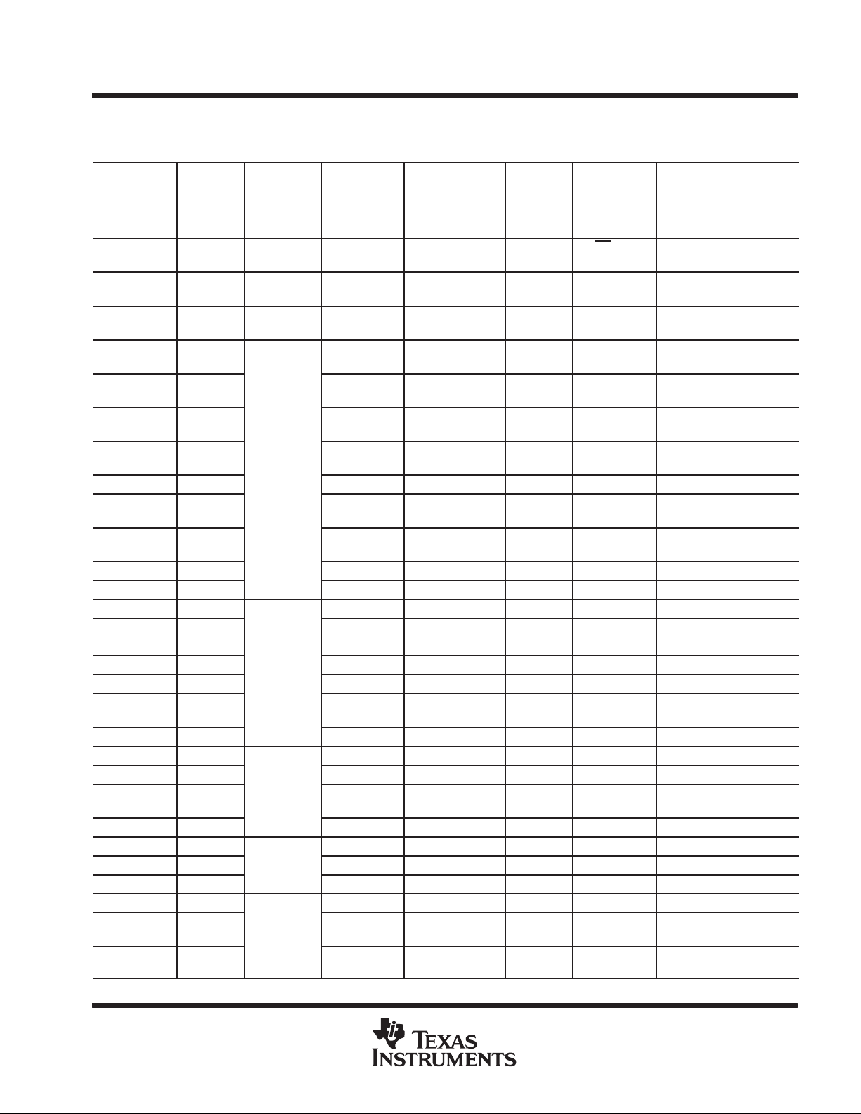
device features
Table 1 and Table 2 provide a comparison of the features of the ’C242 to the ’F241. See the functional block
diagram for the ’C242 peripherals and memory.
Table 1. Hardware Features of the TMS320x24x DSP Controllers
ON-CHIP MEMORY (WORDS)
TMS320x24x
DEVICES
TMS320C242
TMS320F241
DATA SPACE
(B1 RAM - 256 WORDS)
(B2 RAM - 32 WORDS)
288 256 – 5 50
RAM
CONFIGURABLE
DATA/PROG SPACE
(B0 RAM)
EXTERNAL
MEMORY
INTERFA
E
Table 2. Device Specifications of the TMS320x24x DSP Controllers
POWER CYCLE
SUPPLY
(V)
TIME
(ns)
ON-CHIP MEMORY (WORDS)
TMS320x24x
DEVICES
TMS320C242 4K –
TMS320F241 – 8K
ROM
PROG PROG
FLASH
EEPROM
ADC
CHANNELS
8
PERIPHERALS
CAN SPI
– –
√ √
GPIO
26
PACKAGE
TYPE
FN 68-PLCC
PG 64-PQFP
POST OFFICE BOX 1443 • HOUSTON, TEXAS 77251–1443
3
TMS320C242
ADVANCE
INFORMATION
DSP CONTROLLER
SPRS063B – DECEMBER 1997 – REVISED DECEMBER 1999
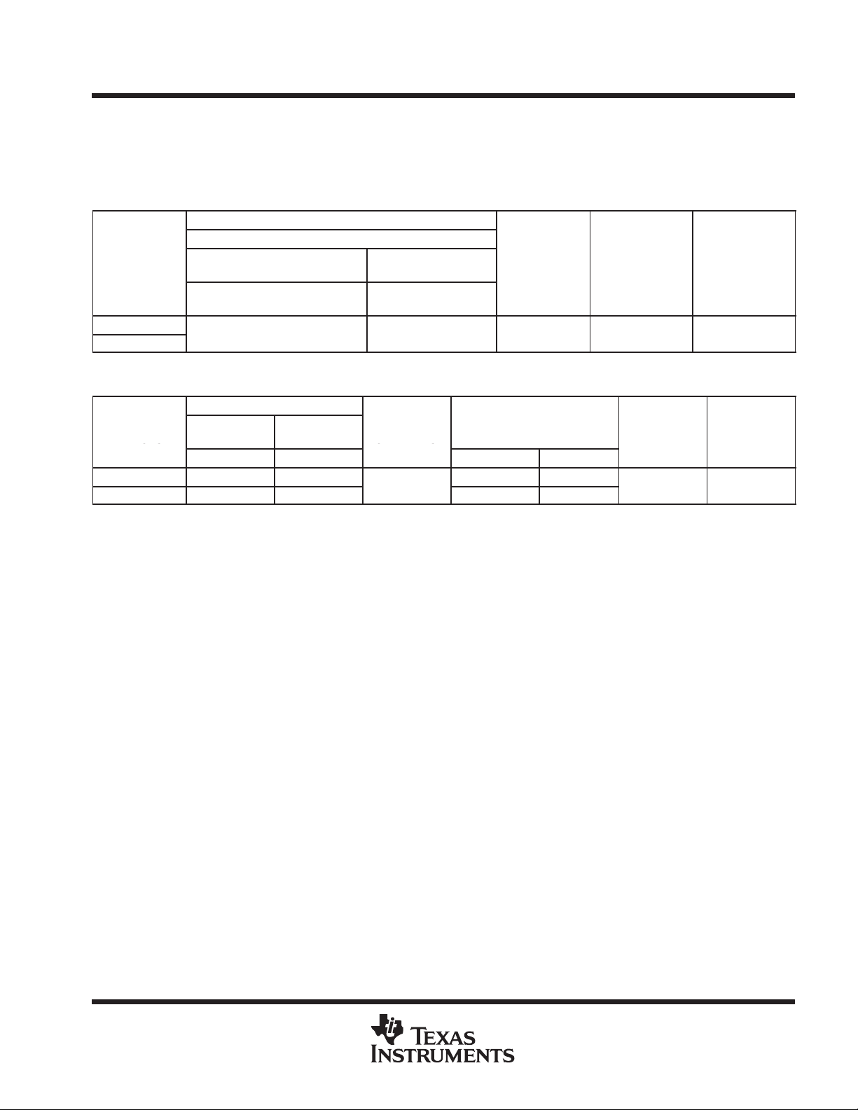
pinouts
IOPC7
IOPC6
CLKOUT/IOPD0
CAP3/IOPA5
CAP2/QEP1/IOPA4
CAP1/QEP0/IOPA3
V
DD
V
SS
T2CMP/T2PWM/IOPB5
T1CMP/T1PWM/IOPB4
V
SSA
V
CCA
ADCIN07
V
REFHI
V
REFLO
ADCIN06
ADCIN05
PDPINT
35 36 37 38 3927
†
TCLKIN/IOPB7
TDIR/IOPB6
XINT1/IOPA2
SSO
XINT2/ADCSOC/IOPD1
NMI
40 41 42 43
DDO
V
WDDIS
V
60
59
58
57
56
55
54
53
52
51
50
49
48
47
46
45
44
PMT
IOPC5
IOPC4
IOPC3
IOPC2
SCIRXD/IOPA1
SCITXD/IOPA0
/IOPC1
BIO
V
DD
V
SS
XF/IOPC0
EMU1
EMU0
XTAL2
XTAL1/CLKIN
V
DDO
V
SSO
FN PACKAGE
(TOP VIEW)
DDO
SSO
PWM1/IOPA6
V
V
87654321686766659 64636261
10
11
12
13
14
15
16
17
18
19
20
21
22
23
24
25
26
28 29 30 31 32 33 34
PWM2/IOPA7
PWM3/IOPB0
PWM4/IOPB1
PWM5/IOPB2
PWM6/IOPB3
TMS320C242
(68-Pin PLCC)
4
NC
ADCIN04
†
NC = No connection, DNC = Do not connect
RS
TDI
SSO
DNC
V
ADCIN01
ADCIN02
ADCIN03
POST OFFICE BOX 1443 • HOUSTON, TEXAS 77251–1443
ADCIN00
TCK
TDO
TMS
V
TRST
SS
DDO
V
SSO
V
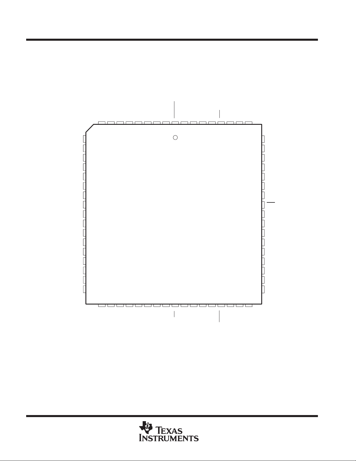
pinouts (continued)
ADVANCE
INFORMATION
XINT2/ADCSOC/IOPD1
XINT1/IOPA2
TDIR/IOPB6
TCLKIN/IOPB7
PWM6/IOPB3
PWM5/IOPB2
PWM4/IOPB1
PWM3/IOPB0
PWM2/IOPA7
PWM1/IOPA6
WDDIS
NMI
PDPINT
SPRS063B – DECEMBER 1997 – REVISED DECEMBER 1999
PG PACKAGE
(TOP VIEW)
SSO
DDO
PMT
IOPC5
IOPC4
IOPC3
IOPC2
V
V
51 50 494847 46 45 44 43 42 41 4039 38 37 36 35 34 33
52
53
54
55
56
57
58
59
60
61
62
63
64
1 2 3 4 5 6 7 8 9 10 11 1213 14 15 16 17 18 19
SCIRXD/IOPA1
TMS320C242
(64-Pin QFP)
†
DD
SCITXD/IOPA0
BIO/IOPC1
XF/IOPC0
VSSV
EMU1
EMU0
XTAL2
SSO
DDO
XTAL1/CLKIN
V
V
32
31
30
29
28
27
26
25
24
23
22
21
20
TMS320C242
DSP CONTROLLER
TRST
TMS
TDO
TDI
TCK
RS
V
SSO
DNC
ADCIN00
ADCIN01
ADCIN02
ADCIN03
ADCIN04
SSO
DDO
V
V
IOPC7
†
NC = No connection, DNC = Do not connect
IOPC6
CAP3/IOPA5
CLKOUT/IOPD0
CAP2/QEP1/IOPA4
CAP1/QEP0/IOPA3
VDDV
SS
SSA
CCA
V
V
T2CMP/T2PWM/IOPB5
T1CMP/T1PWM/IOPB4
REFHI
REFLO
V
V
ADCIN07
ADCIN06
ADCIN05
POST OFFICE BOX 1443 • HOUSTON, TEXAS 77251–1443
5
TMS320C242
NAME
TYPE
†
‡
DESCRIPTION
I
ADVANCE
INFORMATION
DSP CONTROLLER
SPRS063B – DECEMBER 1997 – REVISED DECEMBER 1999
Terminal Functions - ’C242 PG and FN Packages
WDDIS 52 63 I I
ADCIN00 24 32
ADCIN01 23 31
ADCIN02 22 30
ADCIN03 21 29
ADCIN04 20 28
ADCIN05 19 26
ADCIN06 18 25
ADCIN07 15 22
V
CCA
V
SSA
V
REFHI
V
REFLO
T1CMP/T1PWM/
T2CMP/T2PWM/
TDIR/
TCLKIN/
CAP1/QEP0/
CAP2/QEP1/
CAP3/
PWM1/
PWM2/
PWM3/
PWM4/
PWM5/
PWM6/IOPB3 59 2 I/O/Z Compare/PWM output pin #6 or GPIO
PDPINT 58 1 I I
†
I = input, O = output, Z = high impedance
‡
The reset state indicates the state of the pin at reset. If the pin is an input, indicated by an I, its state is determined by user design. If the pin is
an output, its level at reset is indicated.
§
These pins are internally pulled high. However, these pins are not pulled high in the emulation devices (’F243/’F241).
NOTE:
64-PIN
NAME
IOPB4
IOPB5
IOPB6
IOPB7
IOPA3
IOPA4
IOPA5
IOPA6
IOPA7
IOPB0
IOPB1
IOPB2
Bold, italicized pin names
QFP
NO. NO.
14 21 – –
13 20 – – Analog ground reference for ADC
16 23 – – ADC analog high-voltage reference input
17 24 – – ADC analog low-voltage reference input
12 19 I/O/Z Timer 1 compare output/general-purpose bidirectional digital I/O (GPIO).
11 18 I/O/Z Timer 2 compare output/GPIO
56 67 I/O
57 68 I/O
8 15 I/O Capture input #1/quadrature encoder pulse input #0/GPIO
7 14 I/O
6 13 I/O
64 7 I/O/Z Compare/PWM output pin #1 or GPIO
63 6 I/O/Z Compare/PWM output pin #2 or GPIO
62 5 I/O/Z Compare/PWM output pin #3 or GPIO
61 4 I/O/Z Compare/PWM output pin #4 or GPIO
60 3 I/O/Z Compare/PWM output pin #5 or GPIO
68-PIN
PLCC
indicate pin function after reset.
TYPE
ANALOG-TO-DIGITAL CONVERTER (ADC) INPUTS
RESET
†
STATE
INTERFACE CONTROL SIGNALS
Watchdog disable. Note that on ROM devices, only the WDDIS function
is valid. If the input is low, the watchdog timer cannot be disabled in the
software. If the input is high, the watchdog timer can be disabled in the
software through the WDDIS bit in the WDCR register.
I I Analog inputs to the ADC
Analog supply voltage for ADC (5 V). V
digital supply voltage.
EVENT MANAGER
Counting direction for GP timer/GPIO. If TDIR=1, upward counting is
selected. If TDIR=0, downward counting is selected.
External clock input for GP timer/GPIO. Note that timer can also use
the internal device clock.
Capture input #2/quadrature encoder pulse input #1/GPIO
Capture input #3/GPIO
Power drive protection interrupt input. This interrupt, when activated, puts
the PWM output pins in the high-impedance state, should motor
drive/power converter abnormalities, such as overvoltage or overcurrent,
etc., arise. PDPINT
edge, this pin must be held low for two clock cycles for the core to
recognize the interrupt.
DESCRIPTION
must be isolated from
CCA
is a falling-edge-sensitive interrupt. After the falling
6
POST OFFICE BOX 1443 • HOUSTON, TEXAS 77251–1443
SPRS063B – DECEMBER 1997 – REVISED DECEMBER 1999
NAME
TYPE
†
‡
DESCRIPTION
ADVANCE
INFORMATION
Terminal Functions - ’C242 PG and FN Packages (Continued)
TMS320C242
DSP CONTROLLER
64-PIN
NAME
IOPC2
IOPC3
IOPC4
IOPC5
IOPC6
IOPC7
SCITXD/
SCIRXD/
RS 27 35 I/O I
NMI
XINT1/
XINT2/ADCSOC/
XF
BIO/
PMT 49 60 I I Do not connect. Reserved for test.
XTAL1/CLKIN 35 46 I I
XTAL2 36 47 O O
†
‡
§
NOTE:
IOPA0
IOPA1
§
IOPA2
IOPD1
§
/IOPC0
§
IOPC1
I = input, O = output, Z = high impedance
The reset state indicates the state of the pin at reset. If the pin is an input, indicated by an I, its state is determined by user design. If the pin is
an output, its level at reset is indicated.
These pins are internally pulled high. However, these pins are not pulled high in the emulation devices (’F243/’F241).
Bold, italicized pin names
QFP
NO. NO.
68-PIN
PLCC
45 56 I/O GPIO
46 57 I/O GPIO
47 58 I/O
48 59 I/O
4 11 I/O GPIO
3 10 I/O GPIO
SERIAL COMMUNICATIONS INTERFACE (SCI) AND BIT I/O PINS
43 54 I/O
44 55 I/O
INTERRUPT, EXTERNAL ACCESS, AND MISCELLANEOUS SIGNALS
53 64 I I
55 66 I/O I
54 65 I/O I
39 50 I/O O – 1
42 53 I/O I
indicate pin function after reset.
TYPE
RESET
†
STATE
BIT I/O PINS
I
I
CLOCK SIGNALS
DESCRIPTION
GPIO
GPIO
SCI asynchronous serial port transmit data or GPIO
SCI asynchronous serial port receive data or GPIO
Device reset. RS causes the ’C242 to terminate execution and sets
PC=0. After RS
zero of program memory. RS
status bits. When the watchdog timer overflows, it initiates a system reset
pulse that is reflected on the RS
Nonmaskable interrupt. When NMI is activated, the device is interrupted
regardless of the state of the INTM bit of the status register. NMI
(falling) edge- and low-level-sensitive. T o be recognized by the core, this
pin must be kept low for at least one clock cycle after the falling edge.
External user interrupt 1 or GPIO. Both XINT1 and XINT2 are edgesensitive. T o be recognized by the core, these pins must be kept low/high
for at least one clock cycle after the edge. The edge polarity is
programmable.
External user interrupt 2. External “start-of-conversion” input for
ADC/GPIO. Both XINT1 and XINT2 are edge-sensitive. To be
recognized by the core, these pins must be kept low/high for at least one
clock cycle after the edge. The edge polarity is programmable.
External flag output (latched software-programmable signal). XF is a
general-purpose output pin. It is set/reset by the SETC XF/CLRC XF
instruction. This pin is configured as an external flag output by all device
resets. It can be used as a GPIO, if not used as XF.
Branch control input. BIO is polled by the BCND pma,BIO instruction. If
is low, a branch is executed. If BIO is not used, it should be pulled
BIO
high. This pin is configured as a branch control input by all device resets.
It can be used as a GPIO, if not used as a branch control input.
PLL oscillator input pin. Crystal input to PLL/clock source input to
PLL. XTAL1/CLKIN is tied to one side of a reference crystal.
Crystal output. PLL oscillator output pin. XTAL2 is tied to one side of a
reference crystal. This pin goes in the high-impedance state when
EMU1/OFF
is brought to a high level, execution begins at location
is active low.
affects (sets to zero) various registers and
pin. This pulse is eight clock cycles wide.
is
POST OFFICE BOX 1443 • HOUSTON, TEXAS 77251–1443
7
TMS320C242
NAME
TYPE
†
‡
DESCRIPTION
V
SS
Digital logic ground reference
V
SSO
Digital logic and buffer ground reference
ADVANCE
INFORMATION
DSP CONTROLLER
SPRS063B – DECEMBER 1997 – REVISED DECEMBER 1999
Terminal Functions - ’C242 PG and FN Packages (Continued)
CLKOUT
TCK 28 36 I I JTAG test clock with internal pullup
TDI 29 37 I I
TDO 30 38 O O
TMS 31 39 I I
TRST 32 40 I I
EMU0 37 48 I/O I
EMU1 38 49 I/O I
V
DD
V
DDO
V
SS
V
SSO
NC – 27 No internal connection made to this pin
DNC 25 33 – – Do not connect. Reserved for test.
†
I = input, O = output, Z = high impedance
‡
The reset state indicates the state of the pin at reset. If the pin is an input, indicated by an I, its state is determined by user design. If the pin is
an output, its level at reset is indicated.
§
These pins are internally pulled high. However, these pins are not pulled high in the emulation devices (’F243/’F241).
NOTE:
64-PIN
NAME
/IOPD0 5 12 I/O O
Bold, italicized pin names
QFP
NO. NO.
68-PIN
PLCC
9 16 – –
41 52 – –
– 42 – –
1 8 – –
34 45 – –
51 62 – –
– 41 – –
10 17 – –
40 51 – –
– 43 – –
2 9 – –
26 34 – –
33 44 – –
50 61 – –
indicate pin function after reset.
†
TYPE
CLOCK SIGNALS (CONTINUED)
RESET
STATE
Clock output. This pin outputs the CPU clock (CLKOUT) only. This pin can
be used as a GPIO, if it is not used as a clock output pin.
TEST SIGNALS
JTAG test data input (TDI) with internal pullup. TDI is clocked into the
selected register (instruction or data) on a rising edge of TCK.
JTAG scan out, test data output (TDO). The contents of the selected
register (instruction or data) is shifted out of TDO on the falling edge of
TCK.
JTAG test-mode select (TMS) with internal pullup. This serial control
input is clocked into the TAP controller on the rising edge of TCK.
JTAG test reset with internal pulldown. TRST, when driven high, gives
the scan system control of the operations of the device. If this signal is
not connected or driven low, the device operates in its functional mode,
and the test reset signals are ignored.
Emulator I/O pin 0 with internal pullup. When TRST is driven high, this pin
is used as an interrupt to or from the emulator system and is defined as
input/output through the JTAG scan.
Emulator I/O pin 1 with internal pullup. When TRST is driven high, this pin
is used as an interrupt to or from the emulator system and is defined as
input/output through JTAG scan.
SUPPLY SIGNALS
Digital logic supply voltage (5 V)
Digital logic and buffer supply voltage (5 V)
Digital logic ground reference
Digital logic and buffer ground reference
NO CONNECT
DESCRIPTION
8
POST OFFICE BOX 1443 • HOUSTON, TEXAS 77251–1443
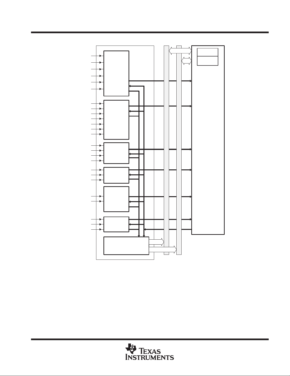
functional block diagram of the ’24x DSP controller
ÁÁÁÁ
ÁÁÁÁ
ÁÁÁÁ
ÁÁÁÁ
ÁÁÁÁ
Á
ADVANCE
INFORMATION
Data Bus
TMS320C242
DSP CONTROLLER
SPRS063B – DECEMBER 1997 – REVISED DECEMBER 1999
Interrupts
Initialization
Program Bus
Program
Controller
ROM
Instruction
Register
ARAU
Status/
Control
Registers
Auxiliary
Registers
Memory
Mapped
Registers
DARAM
B0
Input
Shifter
ALU
Accumulator
Output
Shifter
DARAM
B1/B2
Multiplier
TREG
PREG
Product
Shifter
’C2xx
CPU
Test/
Emulation
Event
Manager
General-
Purpose
Timers
Compare
Units
Capture/
Quadrature
Encoder
Pulse (QEP)
7
2
8
3
Interrupts
4
2
General-
Purpose
I/O Pins
Clock
16
Module
Single 10-Bit
Analog-
to-Digital
Converter
26
POST OFFICE BOX 1443 • HOUSTON, TEXAS 77251–1443
Serial-
Communications
Interface
28
PDPINT
16
Peripheral Bus
Watchdog
Timer
9

TMS320C242
ADVANCE
INFORMATION
DSP CONTROLLER
SPRS063B – DECEMBER 1997 – REVISED DECEMBER 1999
architectural overview
The functional block diagram provides a high-level description of each component in the ’C242 DSP controllers.
The TMS320x24x devices are composed of three main functional units: a ’C2xx DSP core, internal memory,
and peripherals. In addition to these three functional units, there are several system-level features of the ’C242
that are distributed. These system features include the memory map, device reset, interrupts, digital
input/output (I/O), clock generation, and low-power operation.
system-level functions
device memory map
The ’C242 device implements three separate address spaces for program memory, data memory, and
I/O space. On the ’C242, the first 96 (0–5Fh) data memory locations are either allocated for memory-mapped
registers or reserved. This memory-mapped register space contains various control and status registers,
including those for the CPU.
All the on-chip peripherals of the ’C242 devices are mapped into data memory space. Access to these registers
is made by the CPU instructions addressing their data memory locations. Figure 1 shows the ’C242 memory
map.
10
POST OFFICE BOX 1443 • HOUSTON, TEXAS 77251–1443
ADVANCE
INFORMATION
memory map
Hex
0000
003F
0040
0FBF
0FC0
0FFF
1000
FDFF
FE00
FEFF
FF00
FFFF
Program
Interrupt Vectors
User Code in ROM
Reserved
Reserved
Reserved
On-Chip DARAM
B0† (CNF = 1)
Reserved (CNF = 0)
†
TMS320C242
DSP CONTROLLER
SPRS063B – DECEMBER 1997 – REVISED DECEMBER 1999
Hex
0000
005F
0060
007F
0080
01FF
0200
02FF
0300
03FF
0400
6FFF
7000
73FF
7400
743F
7440
77FF
7800
7FFF
8000
FFFF
Data
Memory-Mapped
Registers/Reserved
Addresses
On-Chip
DARAM B2
Reserved
On-Chip DARAM
(B0)‡ (CNF = 0)
Reserved (CNF = 1)
On-Chip
DARAM (B1)
Illegal
Peripheral Memory-
Mapped Registers
(System,WD, ADC,
SCI, I/O,
Interrupts)
Peripheral
Memory-Mapped
Registers
(Event Manager)
Illegal
Illegal
Illegal
§
On-Chip ROM, (4K)
†
When CNF = 1, addresses FE00h–FEFFh and FF00h–FFFFh are mapped to the same physical block (B0) in program-memory space. For
example, a write to FE00h will have the same effect as a write to FF00h. For simplicity, addresses FE00h–FEFFh are referred to as reserved
when CNF = 1.
‡
When CNF = 0, addresses 0100h–01FFh and 0200h–02FFh are mapped to the same physical block (B0) in data-memory space. For example,
a write to 0100h will have the same effect as a write to 0200h. For simplicity , addresses 0100h–01FFh are referred to as reserved.
§
Addresses 0300h–03FFh and 0400h–04FFh are mapped to the same physical block (B1) in data-memory space. For example, a write to 0400h
has the same effect as a write to 0300h. For simplicity, addresses 0400h–04FFh are referred to as illegal.
NOTE A: There is no external memory space for program, data, global data, or I/O in the ’C242. The GREG register is reserved in the ’C242.
Figure 1. TMS320C242 Memory Map
POST OFFICE BOX 1443 • HOUSTON, TEXAS 77251–1443
11
TMS320C242
ADVANCE
INFORMATION
DSP CONTROLLER
SPRS063B – DECEMBER 1997 – REVISED DECEMBER 1999
peripheral memory map
The system and peripheral control register frame contains all the data, status, and control bits to operate the
system and peripheral modules on the device (excluding the event manager). The register frame is mapped
in the data memory space.
Hex
Reserved
Interrupt-Mask Register
0000
0003
0004
Hex
0000
005F
0060
007F
0080
01FF
0200
02FF
0300
03FF
0400
07FF
0800
6FFF
7000
73FF
7400
743F
7440
77FF
7800
7FFF
8000
Memory-Mapped Registers
and Reserved
On-Chip DARAM B2
Reserved
On-Chip DARAM B0
On-Chip DARAM B1
Reserved
Illegal
Peripheral Frame 1 (PF1)
Peripheral Frame 2 (PF2)
Reserved
Illegal
Global-Memory Allocation
Register
Interrupt Flag Register
Emulation Registers
and Reserved
Illegal
System Configuration and
Control Registers
Watchdog Timer Registers
ADC Control Registers
Reserved
SCI
Illegal
External-Interrupt Registers
Illegal
Digital-I/O Control Registers
Illegal
Reserved
Illegal
0005
0006
0007
005F
7000–700F
7010–701F
7020–702F
7030–703F
7040–704F
7050–705F
7060–706F
7070–707F
7080–708F
7090–709F
70A0–70FF
7100–722F
7230–73FF
12
FFFF
Reserved/
Illegal
Capture & QEP Registers
Interrupt Mask, Vector and
Figure 2. Peripheral Memory Map for ’C242
POST OFFICE BOX 1443 • HOUSTON, TEXAS 77251–1443
General-Purpose
Timer Registers
Compare, PWM, and
Deadband Registers
Flag Registers
Reserved
7400–7408
7411–7419
7420–7429
742C–7431
7432–743F
TMS320C242
ADVANCE
INFORMATION
DSP CONTROLLER
SPRS063B – DECEMBER 1997 – REVISED DECEMBER 1999
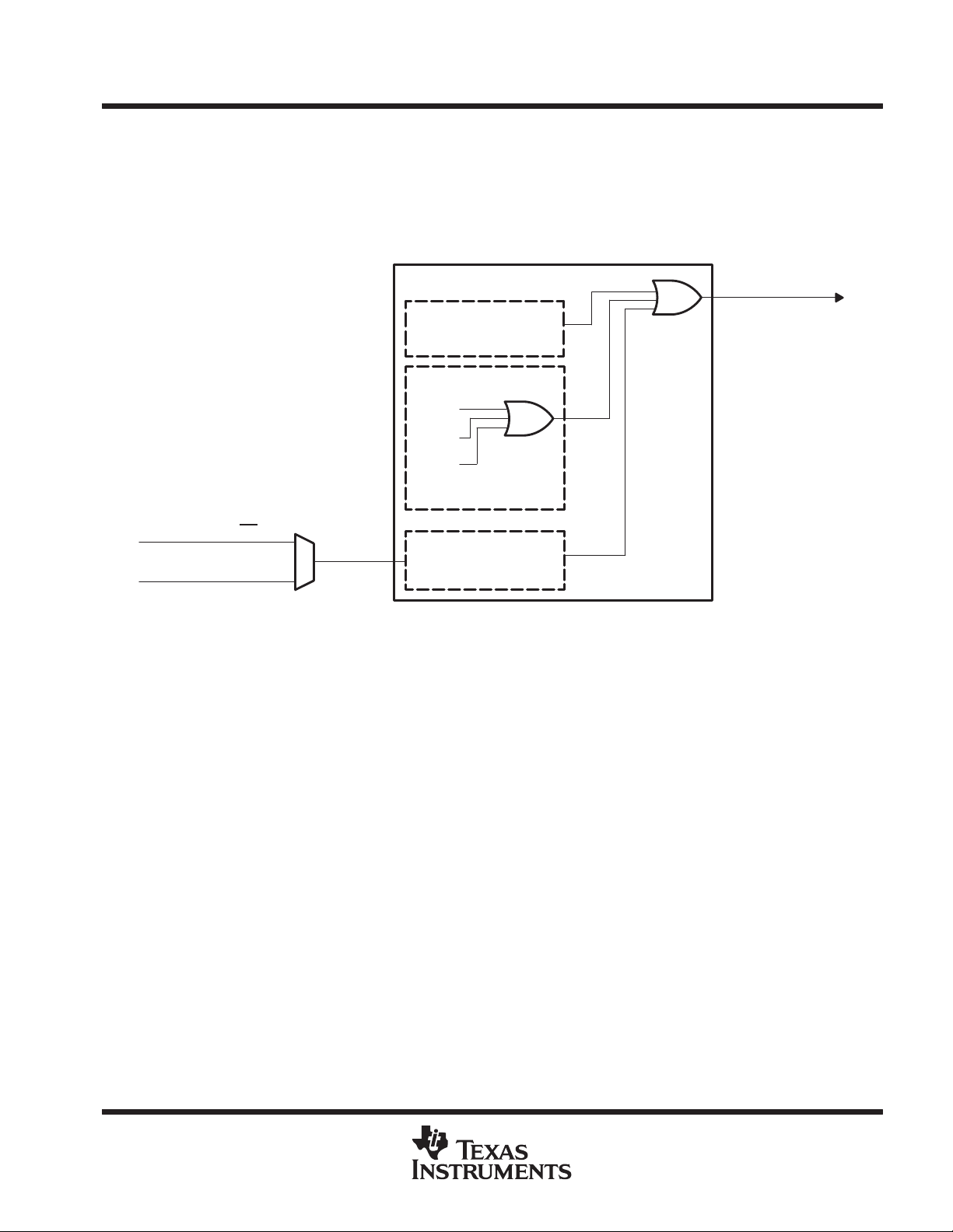
digital I/O and shared pin functions
The ’C242 has a total of 26 general-purpose, bidirectional, digital I/O (GPIO) pins –most of which are shared
between primary functions and I/O. Twenty (20) I/O pins of the ’C242 are shared with other functions. The digital
I/O ports module provides a flexible method for controlling both dedicated I/O and shared pin functions. All I/O
and shared pin functions are controlled using eight 16-bit registers. These registers are divided into two types:
D Output Control Registers — used to control the multiplexer selection that chooses between the primary
function of a pin or the general-purpose I/O function.
D Data and Control Registers — used to control the data and data direction of bidirectional I/O pins.
description of shared I/O pins
The control structure for shared I/O pins is shown in Figure 3, where each pin has three bits that define its
operation:
D Mux control bit — this bit selects between the primary function (1) and I/O function (0) of the pin.
D I/O direction bit — if the I/O function is selected for the pin (mux control bit is set to 0), this bit determines
whether the pin is an input (0) or an output (1).
D I/O data bit — if the I/O function is selected for the pin (mux control bit is set to 0) and the direction selected
is an input, data is read from this bit; if the direction selected is an output, data is written to this bit.
The mux control bit, I/O direction bit, and I/O data bit are in the I/O control registers.
IOP Data Bit
(Read/Write)
In Out
IOP DIR Bit
0 = Input
1 = Output
Primary
Function
or I/O Pin
Primary
Function
01
Pin
Note:
When the MUX control bit = 1, the primary
function is selected in all cases except
for the following pins:
1. XF/IOPC0 (0 = Primary Function)
/IOPC1 (0 = Primary Function)
2. BIO
3. CLKOUT/IOPD0 (0 = Primary Function)
MUX Control Bit
0 = I/O Function
1 = Primary Function
Figure 3. Shared Pin Configuration
A summary of shared pin configurations and associated bits is shown in Table 3.
POST OFFICE BOX 1443 • HOUSTON, TEXAS 77251–1443
13
TMS320C242
MUX CONTROL
ADVANCE
INFORMATION
DSP CONTROLLER
SPRS063B – DECEMBER 1997 – REVISED DECEMBER 1999
description of shared I/O pins (continued)
68-PIN
PLCC
56
57
58
59
10
†
Valid only if the I/O function is selected on the pin
‡
If the GPIO pin is configured as an output, these bits can be written to. If the pin is configured as an input, these bits are read from.
§
If the DIR bit is 0, the GPIO pin functions as an input. For a value of 1, the pin is configured as an output.
¶
Dedicated I/O pins
Table 3. Shared Pin Configurations
PIN NO.
64-PIN
QFP
54 43 OCRA.0 SCITXD IOPA0 PADATDIR 0 8
55 44 OCRA.1 SCIRXD IOPA1 PADATDIR 1 9
66 55 OCRA.2 XINT1 IOPA2 PADATDIR 2 10
15 8 OCRA.3 CAP1/QEP0 IOPA3 PADATDIR 3 11
14 7 OCRA.4 CAP2/QEP1 IOPA4 PADATDIR 4 12
13 6 OCRA.5 CAP3 IOPA5 PADATDIR 5 13
7 64 OCRA.6 PWM1 IOPA6 PADATDIR 6 14
6 63 OCRA.7 PWM2 IOPA7 PADATDIR 7 15
5 62 OCRA.8 PWM3 IOPB0 PBDATDIR 0 8
4 61 OCRA.9 PWM4 IOPB1 PBDATDIR 1 9
3 60 OCRA.10 PWM5 IOPB2 PBDATDIR 2 10
2 59 OCRA.11 PWM6 IOPB3 PBDATDIR 3 11
19 12 OCRA.12 T1PWM/T1CMP IOPB4 PBDATDIR 4 12
18 11 OCRA.13 T2PWM/T2CMP IOPB5 PBDATDIR 5 13
67 56 OCRA.14 TDIR IOPB6 PBDATDIR 6 14
68 57 OCRA.15 TCLKIN IOPB7 PBDATDIR 7 15
50 39 OCRB.0 IOPC0 XF PCDATDIR 0 8
53 42 OCRB.1 IOPC1 BIO PCDATDIR 1 9
¶
45
¶
46
¶
47
¶
48
¶
11
12 5 OCRB.8 IOPD0 CLKOUT PDDATDIR 0 8
65 54 OCRB.9 XINT2/ADCSOC IOPD1 PDDATDIR 1 9
4
¶
3
¶
¶
¶
¶
¶
¶
MUX CONTROL
REGISTER
(name.bit #)
OCRB.2 – IOPC2 PCDATDIR 2 10
OCRB.3 – IOPC3 PCDATDIR 3 11
OCRB.4 – IOPC4 PCDATDIR 4 12
OCRB.5 – IOPC5 PCDATDIR 5 13
OCRB.6 – IOPC6 PCDATDIR 6 14
OCRB.7 – IOPC7 PCDATDIR 7 15
PIN FUNCTION SELECTED I/O PORT DATA AND DIRECTION
(OCRx.n = 1) (OCRx.n = 0) REGISTER
PORT A
PORT B
PORT C
PORT D
DATA BIT
‡
NO.
†
DIR BIT
NO.
§
14
POST OFFICE BOX 1443 • HOUSTON, TEXAS 77251–1443
TMS320C242
ADV ANCE
INFORMATION
DSP CONTROLLER
SPRS063B – DECEMBER 1997 – REVISED DECEMBER 1999
digital I/O control registers
Table 4 lists the registers available in the digital I/O module. As with other ’C242 peripherals, the registers are
memory-mapped to the data space.
Table 4. Addresses of Digital I/O Control Registers
ADDRESS REGISTER NAME
7090h OCRA I/O mux control register A
7092h OCRB I/O mux control register B
7098h PADATDIR I/O port A data and direction register
709Ah PBDATDIR I/O port B data and direction register
709Ch PCDATDIR I/O port C data and direction register
709Eh PDDATDIR I/O port D data and direction register
device reset and interrupts
The TMS320x24x software-programmable interrupt structure supports flexible on-chip and external interrupt
configurations to meet real-time interrupt-driven application requirements. The ’C242 recognizes three types of
interrupt sources:
D Reset (hardware- or software-initiated) is unarbitrated by the CPU and takes immediate priority over any
other executing functions. All maskable interrupts are disabled until the reset service routine enables them.
The ’C242 device has two sources of reset: an external reset pin and a watchdog timer timeout (reset).
D Hardware-generated interrupts are requested by external pins or by on-chip peripherals. There are two
types:
–
External interrupts
XINT2, PDPINT , and NMI. The first three can be masked both by dedicated enable bits and by the C PU’s
interrupt mask register (IMR), which can mask each maskable interrupt line at the DSP core. NMI, which
is not maskable, takes priority over peripheral interrupts and software-generated interrupts. It can be
locked out only by an already executing NMI
Peripheral interrupts
–
SCI, WD, and ADC. They can be masked both by enable bits for each eve nt in each perip heral and by the
CPU’s IMR, which can mask each maskable interrupt line at the DSP core.
are generated by one of four external pins corresponding to the interrupts XINT1,
or a reset.
are initiated internally by these on-chip peripheral modules: the event manager,
D Software-generated interrupts for the ’C242 include:
The INTR instruction.
–
operand indicates the interrupt vector location to which the CPU branches. This instruction globally
disables maskable interrupts (sets the INTM bit to 1).
–
The NMI instruction.
used for the nonmaskable hardware interrupt NMI. NMI can be initiated by driving the NMI
executing an NMI instruction. This instruction globally disables maskable interrupts.
–
The TRAP instruction.
TRAP instruction does
branches to the interrupt service routine, that routine can be interrupted by the maskable hardware
interrupts.
This instruction allows initialization of any ’C242 interrupt with software. Its
This instruction forces a branch to interrupt vector location 24h, the same location
pin low or by
This instruction forces the CPU to branch to interrupt vector location 22h. The
not
disable maskable interrupts (INTM is not set to 1); therefore, when the CPU
–
An emulator trap.
This interrupt can be generated with either an INTR instruction or a TRAP instruction.
POST OFFICE BOX 1443 • HOUSTON, TEXAS 77251–1443
15

TMS320C242
ADVANCE
INFORMATION
DSP CONTROLLER
SPRS063B – DECEMBER 1997 – REVISED DECEMBER 1999
reset
The reset operation ensures an orderly startup sequence for the device. There are two possible causes of a
reset, as shown in Figure 4.
Reset
Watchdog Timer Reset
External Reset (RS) Pin Active
Figure 4. Reset Signals
The two possible reset signals are generated as follows:
D Watchdog timer reset. A watchdog-timer-generated reset occurs if the watchdog timer overflows or an
improper value is written to either the watchdog key register or the watchdog control register. (Note that
when the device is powered on, the watchdog timer is automatically active.) The watchdog timer reset is
reflected on the external RS
pin also.
D Reset pin active. To generate an external reset pulse on the RS pin, a low-level pulse duration of at least
one CPUCLK cycle is necessary to ensure that the device recognizes the reset signal.
Signal
System Reset
hardware-generated interrupts
Once watchdog reset is activated, the external RS
cycles. This allows the TMS320x24x device to reset external system components.
The occurrence of a reset condition causes the TMS320x24x to terminate program execution and affects
various registers and status bits. During a reset, RAM contents remain unchanged, and all control bits that are
affected by a reset are initialized to their reset state.
The ’24x CPU supports one nonmaskable interrupt (NMI) and six maskable prioritized interrupt requests. The
’24x devices have many peripherals, and each peripheral is capable of generating one or more interrupts in
response to many events. The ’24x CPU does not have sufficient interrupt requests to handle all these
peripheral interrupt requests; therefore, a centralized interrupt controller is provided to arbitrate the interrupt
requests from all the different sources. Throughout this section, refer to Figure 5 .
pin is driven (active) low for a minimum of eight CPUCLK
16
POST OFFICE BOX 1443 • HOUSTON, TEXAS 77251–1443
hardware-generated interrupts (continued)
ADVANCE
INFORMATION
TMS320C242
DSP CONTROLLER
SPRS063B – DECEMBER 1997 – REVISED DECEMBER 1999
PDPINT
ADCINT
XINT1
XINT2
RXINT
TXINT
CMP1INT
CMP2INT
CMP3INT
TPINT1
TCINT1
TUFINT1
TOFINT1
TPINT2
TCINT2
TUFINT2
TOFINT2
CAPINT1
CAPINT2
CAPINT3
Level 1
IRQ GEN
Level 2
IRQ GEN
Level 3
IRQ GEN
Level 4
IRQ GEN
PIE
IMR
IFR
INT1
INT2
CPU
INT3
INT4
RXINT
TXINT
ADCINT
XINT1
XINT2
Peripheral Interrupt Requests
(PIRQs)
Level 5
IRQ GEN
Level 6
IRQ GEN
PIVR & logic
PIRQR#
PIACK#
Data
Bus
Addr
Bus
INT5
INT6
IACK
Figure 5. Peripheral Interrupt Expansion Block Diagram
interrupt hierarchy
The number of interrupt requests available is expanded by having two levels of hierarchy in the interrupt request
system. There are two levels of hierarchy in both the interrupt request/acknowledge hardware and in the
interrupt service routine software.
POST OFFICE BOX 1443 • HOUSTON, TEXAS 77251–1443
17

TMS320C242
ADVANCE
INFORMATION
DSP CONTROLLER
SPRS063B – DECEMBER 1997 – REVISED DECEMBER 1999
interrupt request structure
1. At the lower level of the hierarchy , the peripheral interrupt requests (PIRQs) from several peripherals to the
interrupt controller are ORed together to generate a request to the CPU. There is an interrupt flag bit and
an interrupt enable bit located in the peripheral for each event that can cause a peripheral interrupt request.
There is also one PIRQ for each event. If an interrupt-causing event occurs in a peripheral, and the
corresponding interrupt enable bit is set, the interrupt request from the peripheral to the interrupt controller
is asserted. This interrupt request simply reflects the status of the peripheral’s interrupt flag gated with the
interrupt enable bit. When the interrupt flag is cleared, the interrupt request is cleared. Some peripherals
have the capability to make either a high-priority or a low-priority interrupt request. If a peripheral has this
capability , the value of its interrupt priority bit is transmitted to the interrupt controller . The interrupt request
continues to be asserted until it is either automatically cleared by an interrupt acknowledge or cleared by
software.
2. At the upper level of the hierarchy, the ORed PIRQs generate interrupt (INT) requests to the CPU. The
request to the ’24x CPU is a low-going pulse of 2 CPU clock cycles. The Peripheral Interrupt Expansion
(PIE) controller generates an INT pulse when any of the PIRQs controlling that INT go active. If any of the
PIRQs capable of asserting that CPU interrupt request are still active in the cycle following an interrupt
acknowledge for that INT, another INT pulse is generated in the PIE. Each INT request is followed by an
interrupt acknowledge from the CPU, which helps to clear the interrupt-causing flag in the PIE. The interrupt
controller defines which CPU interrupt requests get asserted by which peripheral interrupt requests, and
the relative priority of each peripheral interrupt request. Thus, priority is determined by the interrupt
controller and is not part of any of the peripherals. Table 5 lists interrupt source priority and vectors.
18
POST OFFICE BOX 1443 • HOUSTON, TEXAS 77251–1443
interrupt request structure (continued)
INT2
INT3
0008h
000Ah
ADVANCE
INFORMATION
Table 5. ’C242 Interrupt Source Priority and Vectors
TMS320C242
DSP CONTROLLER
SPRS063B – DECEMBER 1997 – REVISED DECEMBER 1999
CPU
INTERRUPT
NAME
Reset 1
Reserved 2
NMI 3
PDPINT 4 0.0 0020h Y EV
ADCINT 5 0.1 0004h Y ADC
XINT1 6 0.2 0001h Y
XINT2 7
Reserved 8
RXINT 9 0.5 0006h Y SCI
TXINT 10 0.6 0007h Y SCI
Reserved 11
Reserved 12
CMP1INT 13 0.9 0021h Y EV Compare 1 interrupt
CMP2INT 14 0.10 0022h Y EV Compare 2 interrupt
CMP3INT 15 0.11 0023h Y EV Compare 3 interrupt
TPINT1 16
TCINT1 17
TUFINT1 18 0.14 0029h Y EV
TOFINT1 19 0.15 002Ah Y EV Timer 1 overflow interrupt
TPINT2 20 1.0 002Bh Y EV Timer 2 period interrupt
TCINT2 21
TUFINT2 22
TOFINT2 23 1.3 002Eh Y EV Timer 2 overflow interrupt
CAPINT1 24
CAPINT2 25
CAPINT3 26
Reserved 27
RXINT 28
TXINT 29
OVERALL
PRIORITY
INTERRUPT
AND
VECTOR
ADDRESS
RSN
0000h
–
0026h
NMI
0024h
INT1
0002h
INT2
0004h
INT3
0006h
INT4
INT5
BIT
POSITION IN
PIRQRx AND
PIACKRx
0.3 0011h Y
0.12 0027h Y EV Timer 1 period interrupt
0.13 0028h Y EV Timer 1 PWM interrupt
1.1 002Ch Y EV Timer 2 PWM interrupt
1.2 002Dh Y EV
1.4 0033h Y EV Capture 1 interrupt
1.5 0034h Y EV Capture 2 interrupt
1.6 0035h Y EV Capture 3 interrupt
1.8 0006h Y SCI
1.9 0007h Y SCI
PERIPHERAL
INTERRUPT
VECTOR
(PIV)
N/A N
N/A N CPU Emulator Trap
N/A N
MASKABLE?
SOURCE
PERIPHERAL
MODULE
RS pin,
Watchdog
Nonmaskable
Interrupt
External
Interrupt Logic
External
Interrupt Logic
Reset from pin, watchdog
timeout
Nonmaskable interrupt
Power device protection
interrupt pin
ADC interrupt in
high-priority mode
External interrupt pins in
high priority
External interrupt pins in
high priority
SCI receiver interrupt in
high-priority mode
SCI transmitter interrupt
in high-priority mode
Timer 1 underflow
interrupt
Timer 2 underflow
interrupt
SCI receiver interrupt
(low-priority mode)
SCI transmitter interrupt
(low-priority mode)
DESCRIPTION
POST OFFICE BOX 1443 • HOUSTON, TEXAS 77251–1443
19
TMS320C242
INT5
000Ch
ADVANCE
INFORMATION
DSP CONTROLLER
SPRS063B – DECEMBER 1997 – REVISED DECEMBER 1999
interrupt request structure (continued)
Table 5.’C242 Interrupt Source Priority and Vectors (Continued)
†
interrupt acknowledge
CPU
INTERRUPT
NAME
Reserved 30
Reserved 31
ADCINT 32 1.12 0004h Y ADC
XINT1 33
XINT2 34
Reserved 000Eh N/A Y CPU Analysis interrupt
TRAP N/A 0022h N/A N/A CPU TRAP instruction
Phantom
Interrupt
Vector
INT8 through
INT16
INT20 through
INT31
Refer to the
and Peripherals User’s Guide Volume 2
OVERALL
PRIORITY
N/A N/A 0000h N/A CPU
N/A
N/A
TMS320C24x CPU System and Instruction Set, Volume 1
INTERRUPT
AND
VECTOR
ADDRESS
INT5
000Ah
INT6
000Ch
0010h through
0020h
00028h through
0603Fh
(SPRU276) for more information.
BIT
POSITION
IN
PIRQRx
AND
PIACKRx
1.13 0001h Y
1.14 0011h Y
PERIPHERAL
INTERRUPT
VECTOR
(PIV)
N/A N/A CPU
N/A N/A CPU
(SPRU160); and the
MASKABLE?
TMS320F243,F241,C242 DSP Controllers System
SOURCE
PERIPHERAL
MODULE
External
Interrupt Logic
External
Interrupt Logic
DESCRIPTION
ADC interrupt
(low-priority)
External interrupt pins
(low-priority mode)
External interrupt pins
(low-priority mode)
Phantom interrupt
vector
Software
p
Interrupt
†
Vectors
When the CPU asserts its interrupt acknowledge, it simultaneously puts a value on the memory interface
program address bus, which corresponds to the CPU interrupt being acknowledged (it does this because it is
fetching the CPU interrupt vector from program memory , each INT has a vector stored in a dedicated program
memory address). This value is shown in Table 5, column 3, CPU Interrupt and Vector Address. The PIE
controller uses the CPU interrupt acknowledge to generate its internal signals to clear the current interrupt
request.
interrupt vectors
20
When the CPU receives an interrupt request (INT), it does not know which peripheral PIRQ caused the INT
request. T o enable the CPU to distinguish among the PIRQs, a unique interrupt vector is generated in response
to a CPU interrupt acknowledge signal. This vector (PIV) is loaded into the Peripheral Interrupt Vector Register
(PIVR) in the PIE controller. The CPU reads this PIV vector value from PIVR and branches to the respective
Interrupt Service Routine (SISR). The PIVs are all implemented as hard-coded values on the ’C242, according
to Table 5, column 5.
In effect, there are two vector tables: a CPU vector table and a user-specified peripheral vector table. The CPU’s
vector table, which starts at 0000h, is used to get to the General Interrupt Service Routine (GISR) in response
to a CPU interrupt request (INT). A user-specified peripheral vector table is employed to get to the
Event-Specific Interrupt Service Routine (SISR), corresponding to the event which caused the peripheral
interrupt request (PIRQ). The code in the GISR should read the Peripheral Interrupt Vector Register (PIVR) after
saving any necessary context, and use this value PIV to generate a branch to the SISR. There is one SISR for
every interrupt request from a peripheral to the interrupt controller. The SISR performs the actions required in
response to the peripheral interrupt request.
POST OFFICE BOX 1443 • HOUSTON, TEXAS 77251–1443

TMS320C242
ADVANCE
INFORMATION
DSP CONTROLLER
SPRS063B – DECEMBER 1997 – REVISED DECEMBER 1999
interrupt vectors (continued)
phantom interrupt vector
The phantom interrupt vector is an interrupt system integrity feature. If the CPU’s interrupt acknowledge is
asserted, but there is no associated peripheral interrupt request asserted, the phantom vector is used so that
this fault is handled in a controlled manner. One way the phantom interrupt vector could be required is if the CPU
executes a software interrupt instruction with an argument corresponding to a peripheral interrupt (usually
INT1–INT6). The other way would be if a peripheral made an interrupt request, but its interrupt request flag was
cleared by software before the CPU acknowledged the request. In this case, there may be no peripheral
interrupt request asserted to the interrupt controller, so the controller would not know which peripheral interrupt
vector to load into the PIVR. In these situations, the phantom interrupt vector is loaded into the PIVR in lieu of
a peripheral interrupt vector.
nonmaskable interrupts
The PIE controller does not support expansion of nonmaskable interrupts. This is because an ISR must read
the peripheral interrupt vector from the PIVR before interrupts are re-enabled. All interrupts (INT1 – INT6) are
automatically disabled when the CPU branches to each of the respective vectors. If the PIVR is not read before
interrupts are re-enabled (INTM = 0), another interrupt would be acknowledged and a new peripheral interrupt
vector would be loaded into the PIVR, causing permanent loss of the original peripheral interrupt vector. Since,
by their very nature, nonmaskable interrupts cannot be masked, they cannot be included in the interrupt
expansion controller because they could cause the loss of peripheral interrupt vectors.
interrupt operation sequence
1. An interrupt-generating event occurs in a peripheral. The interrupt flag (IF) bit corresponding to that event
is set in a register in the peripheral. If the appropriate interrupt enable (IE) bit is set, the peripheral generates
an interrupt request to the PIE controller by asserting its PIRQ. If the interrupt is not enabled in the peripheral
register, the IF remains set until cleared by software. If the interrupt is enabled at a later time, and the
interrupt flag is still set, the PIRQ will immediately be asserted. The interrupt flag (IF) in the peripheral
register should be cleared by software only . If the IF bit is not cleared after the respective interrupt service,
future interrupts will not be recognized.
2. If no unacknowledged CPU interrupt request of the same priority level has previously been sent, the
peripheral interrupt request, PIRQ, causes the PIE controller to generate a CPU interrupt request pulse.
This pulse is active low for 2 CPU clock cycles.
3. The interrupt request to the CPU sets the corresponding flag in the CPU’s interrupt flag register , IFR. If the
CPU interrupt has been enabled (by setting the appropriate bit in the CPU’s Interrupt Mask Register , IMR),
the CPU stops what it is doing. It then masks all other maskable interrupts by setting the INTM bit, saves
some context, clears the respective IFR bit, and starts executing the General Interrupt Service Routine
(GISR) for that interrupt priority level. The CPU generates an interrupt acknowledge automatically, which
is accompanied by a value on the Program Address Bus (P AB) that corresponds to the interrupt priority level
being responded to. These values are shown in Table 5, column 3.
4. The PIE controller decodes the P AB value and generates an internal peripheral interrupt acknowledge to
load the PIV into the PIVR. The appropriate peripheral interrupt vector (or the phantom interrupt vector),
is referenced from the table stored in the PIE controller.
5. When the GISR has completed any necessary context saves, it reads the PIVR and uses the interrupt vector
as a target (or to generate a target) for a branch to the Event-Specific Interrupt Service Routine (SISR) for
the interrupt event which occurred in the peripheral. Interrupts
been read; otherwise, its contents can get overwritten by a subsequent interrupt.
must not
be re-enabled until the PIVR has
POST OFFICE BOX 1443 • HOUSTON, TEXAS 77251–1443
21

TMS320C242
ADVANCE
INFORMATION
DSP CONTROLLER
SPRS063B – DECEMBER 1997 – REVISED DECEMBER 1999
external interrupts
The ’C242 device has four external interrupts. These interrupts include:
D XINT1. The XINT1 control register (at 7070h) provides control and status for this interrupt. XINT1 can be used
as a high-priority (Level 1) or low-priority (Level 6) maskable interrupt or as a general-purpose I/O pin. XINT1
can also be programmed to trigger an interrupt on either the rising or the falling edge.
D XINT2. The XINT2 control register (at 7071h) provides control and status for this interrupt. XINT2 can be used
as a high-priority (Level 1) or low-priority (Level 6) maskable interrupt or a general-purpose I/O pin. XINT2 can
also be programmed to trigger an interrupt on either the rising or the falling edge.
D NMI. This is a nonmaskable external interrupt.
D PDPINT. This interrupt is provided for safe operation of power converters and motor drives controlled by
the ’C242. This maskable interrupt can put the timers and PWM output pins in high-impedance states and
inform the CPU in case of motor drive abnormalities such as overvoltage, overcurrent, and excessive
temperature rise. PDPINT
Table 6 is a summary of the external interrupt capability of the ’C242.
is a Le vel 1 interrupt.
Table 6. External Interrupt Types and Functions
EXTERNAL
INTERRUPT
XINT1 XINT1CR 7070h
XINT2 XINT2CR 7071h
NMI — — No
PDPINT EVIMRA 742Ch
CONTROL
REGISTER
NAME
CONTROL
REGISTER
ADDRESS
MASKABLE?
Yes
(Level 1 or 6)
Yes
(Level 1 or 6)
Yes
(Level 1)
22
POST OFFICE BOX 1443 • HOUSTON, TEXAS 77251–1443

TMS320C242
ADVANCE
INFORMATION
DSP CONTROLLER
SPRS063B – DECEMBER 1997 – REVISED DECEMBER 1999
clock generation
The ’C242 device has an on-chip, (x4) PLL-based clock module. This module provides all the necessary
clocking signals for the device, as well as control for low-power mode entry. The only external component
necessary for this module is a fundamental crystal. The “times 4” (x4) option for the ’C242 PLL is fixed and
cannot be changed.
The PLL-based clock module provides two modes of operation:
D Crystal-operation
This mode allows the use of a 5-MHz external reference crystal/resonator to provide the time base to the
device.
D External clock source operation
This mode allows the internal oscillator to be bypassed. The device clocks are generated from an external
clock source input on the XTAL1/CLKIN pin. In this case, an external oscillator clock is connected to the
XTAL1/CLKIN pin.
The clock module includes two external pins:
1. XTAL1/CLKIN clock source/crystal input
2. XTAL2 output to crystal
XTAL1/CLKIN
XTAL
OSC
XTAL2
Figure 6. PLL Clock Module Block Diagram
x4
PLL
CPUCLK
low-power modes
The ’24x has an IDLE instruction. When executed, the IDLE instruction stops the clocks to all circuits in the CPU,
but the clock output from the CPU continues to run. With this instruction, the CPU clocks can be shut down to
save power while the peripherals (clocked with CLKOUT) continue to run. The CPU exits the IDLE state if it is
reset, or, if it receives an interrupt request.
clock domains
All ’24x-based devices have two clock domains:
1. CPU clock domain – consists of the clock for most of the CPU logic
2. System clock domain – consists of the peripheral clock (which is derived from CLKOUT of the CPU) and
the clock for the interrupt logic in the CPU.
When the CPU goes into IDLE mode, the CPU clock domain is stopped while the system clock domain continues
to run. This mode is also known as IDLE1 mode. The ’24x CPU also contains support for a second IDLE mode,
IDLE2. By asserting IDLE2 to the ’24x CPU, both the CPU clock domain and the system clock domain are
stopped, allowing further power savings. A third low-power mode, HAL T mode, the deepest, is possible if the
oscillator and WDCLK are also shut down when in IDLE2 mode.
POST OFFICE BOX 1443 • HOUSTON, TEXAS 77251–1443
23

TMS320C242
ADVANCE
INFORMATION
DSP CONTROLLER
SPRS063B – DECEMBER 1997 – REVISED DECEMBER 1999
clock domains (continued)
Two control bits, LPM(1) and LPM(0), specify which of the three possible low-power modes is entered when
the IDLE instruction is executed (see Table 7). These bits are located in the System Control and Status Register
(SCSR) described in the
Volume 2
(literature number SPRU276).
TMS320F243,F241,C242 DSP Controllers System and Peripherals User’s Guide
Table 7. Low-Power Modes Summary
wakeup from low-power modes
reset
external interrupts
LOW-POWER MODE
CPU running normally XX On On On On On —
IDLE1 – (LPM0) 00 Off On On On On
IDLE2 – (LPM1) 01 Off Off On On On
HALT – (LPM2)
{PLL/OSC power down}
LPMx BITS
SCSR[13:12]
1X Of f Off Off Off Off Reset Only
CPU
CLOCK
DOMAIN
SYSTEM
CLOCK
DOMAIN
WDCLK
STATUS
PLL
STATUS
OSC
STATUS
EXIT
CONDITION
Peripheral Interrupt,
External Interrupt,
Reset
Wakeup Interrupts,
External Interrupt,
Reset
A reset (from any source) causes the device to exit any of the IDLE modes. If the device is halted, the reset will
first start the oscillator, and there can be a delay while the oscillator powers up before clocks are generated to
initiate the CPU reset sequence.
The external interrupts, XINTx, can cause the device to exit any of the low-power modes, except HAL T. If the
device is in IDLE2 mode, the synchronous logic connected to the external interrupt pins is bypassed with
combinatorial logic which recognizes the interrupt on the pin, starts the clocks, and then allows the clocked logic
to generate an interrupt request to the PIE controller . Note that in Table 7, external interrupts include PDPINT
.
24
POST OFFICE BOX 1443 • HOUSTON, TEXAS 77251–1443
TMS320C242
ADVANCE
INFORMATION
DSP CONTROLLER
SPRS063B – DECEMBER 1997 – REVISED DECEMBER 1999
wakeup interrupts
Certain peripherals can have the capability to start the device clocks and then generate an interrupt in response
to certain external events, for example, activity on a communication line.
peripheral interrupts
All peripheral interrupts, if enabled locally and globally, can cause the device to exit IDLE1 mode.
External Reset (RS pin)
M
Watchdog Timer Module
(Wake-up Signal)
†
The CPU can exit HALT mode (LPM2) with a RESET only.
U
X
Figure 7. Waking Up the Device From Power Down
Peripheral
Interrupts
NMI
XINT1
XINT2
External-Interrupt Logic
Reset Logic
Reset
Signal
Wake-up Signal
to CPU
†
POST OFFICE BOX 1443 • HOUSTON, TEXAS 77251–1443
25

TMS320C242
ADVANCE
INFORMATION
DSP CONTROLLER
SPRS063B – DECEMBER 1997 – REVISED DECEMBER 1999
functional block diagram of the ’24x DSP CPU
Program Bus
XINT[1–2]
16
XF
RS
Data Bus
Memory Map
2
Register
IMR (16)
IFR (16)
GREG (16)
3
Control
MUXMUX
ARP(3)
ARB(3)
ROM
4K
16
MUX
NPAR
PAR MSTACK
16
16
DP(9)
MUX
MUX
Data
DARAM
B2 (32 × 16)
B1 (256 × 16)
16
Data Bus
MUX
Stack 8 × 16
Program Control
(PCTRL)
16
16
Data Bus
16
MUX
16
16
TREG0(16)
Multiplier
PREG(32)
PSCALE (–6,ā0,ā1,ā4)
MUX
CALU(32)
32
ACCL(16)ACCH(16)C
32
OSCALE (0–7)
16
MUX
32
3232
32
9
7
LSB
from
IR
9
16
ISCALE (0–16)
32
16
Program Bus
1616
16
Program Bus
XTAL2
CLKOUT
XTAL1/
CLKIN
16
PC
NMI
16
16
16
1616
3
AR0(16)
AR1(16)
AR2(16)
ARAU(16)
MUX
Data/Prog
DARAM
B0 (256 × 16)
MUX
16
AR3(16)
AR4(16)
AR5(16)
AR6(16)
AR7(16)
3
3
NOTES: A. Symbol descriptions appear in Table 8 and Table 9.
B. For clarity, the data and program buses are shown as single buses although they include address and data bits.
26
POST OFFICE BOX 1443 • HOUSTON, TEXAS 77251–1443

ADVANCE
INFORMATION
SPRS063B – DECEMBER 1997 – REVISED DECEMBER 1999
’24x legend for the internal hardware functional block diagram
Table 8. Legend for the ’24x Internal Hardware Functional Block Diagram
SYMBOL NAME DESCRIPTION
ACC Accumulator
ARAU
AUX
REGS
BR
C Carry
CALU
DARAM Dual-Access RAM
DP
GREG
IMR
IFR
INT# Interrupt Traps A total of 32 interrupts by way of hardware and/or software are available.
ISCALE
MPY Multiplier
MSTACK Micro Stack
MUX Multiplexer Multiplexes buses to a common input
NPAR
OSCALE
PAR
PC Program Counter
PCTRL
Auxiliary Register
Arithmetic Unit
Auxiliary Registers
0–7
Bus Request
Signal
Central Arithmetic
Logic Unit
Data Memory
Page Pointer
Global Memory
Allocation
Register
Interrupt Mask
Register
Interrupt Flag
Register
Input Data-Scaling
Shifter
Next Program
Address Register
Output
Data-Scaling
Shifter
Program Address
Register
Program
Controller
32-bit register that stores the results and provides input for subsequent CALU operations. Also includes shift
and rotate capabilities
An unsigned, 16-bit arithmetic unit used to calculate indirect addresses using the auxiliary registers as inputs
and outputs
These 16-bit registers are used as pointers to anywhere within the data space address range. They are
operated upon by the ARAU and are selected by the auxiliary register pointer (ARP). AR0 can also be used
as an index value for AR updates of more than one and as a compare value to AR.
BR is asserted during access of the external global data memory space. READY is asserted to the device
when the global data memory is available for the bus transaction. BR
address space by up to 32K words.
Register carry output from CALU. C is fed back into the CALU for extended arithmetic operation. The C bit
resides in status register 1 (ST1), and can be tested in conditional instructions. C is also used in accumulator
shifts and rotates.
32-bit-wide main arithmetic logic unit for the TMS320C2xx core. The CALU executes 32-bit operations in a
single machine cycle. CALU operates on data coming from ISCALE or PSCALE with data from ACC, and
provides status results to PCTRL.
If the on-chip RAM configuration control bit (CNF) is set to 0, the reconfigurable data dual-access RAM
(DARAM) block B0 is mapped to data space; otherwise, B0 is mapped to program space. Blocks B1 and B2
are mapped to data memory space only, at addresses 0300–03FF and 0060–007F, respectively. Blocks 0
and 1 contain 256 words, while Block 2 contains 32 words.
The 9-bit DP register is concatenated with the seven least significant bits (LSBs) of an instruction word to
form a direct memory address of 16 bits. DP can be modified by the LST and LDP instructions.
GREG specifies the size of the global data memory space. This register is reserved in the ’C242 as there
is no external memory interface on this device.
IMR individually masks or enables the seven interrupts.
The 7-bit IFR indicates that the TMS320C2xx has latched an interrupt from one of the seven maskable
interrupts.
16- to 32-bit barrel left-shifter. ISCALE shifts incoming 16-bit data 0 to16 positions left, relative to the 32-bit
output within the fetch cycle; therefore, no cycle overhead is required for input scaling operations.
16 × 16-bit multiplier to a 32-bit product. MPY executes multiplication in a single cycle. MPY operates either
signed or unsigned 2s-complement arithmetic multiply.
MSTACK provides temporary storage for the address of the next instruction to be fetched when program
address-generation logic is used to generate sequential addresses in data space.
NPAR holds the program address to be driven out on the PAB on the next cycle.
16- to 32-bit barrel left-shifter. OSCALE shifts the 32-bit accumulator output 0 to 7 bits left for quantization
management and outputs either the 16-bit high- or low-half of the shifted 32-bit data to the data-write data
bus (DWEB).
PAR holds the address currently being driven on P AB for as many cycles as it takes to complete all memory
operations scheduled for the current bus cycle.
PC increments the value from NPAR to provide sequential addresses for instruction-fetching and sequential
data-transfer operations.
PCTRL decodes instruction, manages the pipeline, stores status, and decodes conditional operations.
can be used to extend the data memory
TMS320C242
DSP CONTROLLER
POST OFFICE BOX 1443 • HOUSTON, TEXAS 77251–1443
27
TMS320C242
ADVANCE
INFORMATION
DSP CONTROLLER
SPRS063B – DECEMBER 1997 – REVISED DECEMBER 1999
’24x legend for the internal hardware functional block diagram (continued)
Table 8. Legend for the ’24x Internal Hardware Functional Block Diagram (Continued)
SYMBOL NAME DESCRIPTION
PREG Product Register 32-bit register holds results of 16 × 16 multiply
0-, 1-, or 4-bit left shift, or 6-bit right shift of multiplier product. The left-shift options are used to manage the
PSCALE
STACK Stack
TREG
Product-Scaling
Shifter
Temporary
Register
’C242 DSP core CPU
The TMS320x24x devices use an advanced Harvard-type architecture that maximizes processing power by
maintaining two separate memory bus structures — program and data — for full-speed execution. This multiple
bus structure allows data and instructions to be read simultaneously. Instructions support data transfers
between program memory and data memory . This architecture permits coefficients that are stored in program
memory to be read in RAM, thereby eliminating the need for a separate coefficient ROM. This, coupled with a
four-deep pipeline, allows the ’C242 to execute most instructions in a single cycle.
additional sign bits resulting from the 2s-complement multiply. The right-shift option is used to scale down
the number to manage overflow of product accumulation in the CALU. PSCALE resides in the path from the
32-bit product shifter and from either the CALU or the data-write data bus (DWEB), and requires no cycle
overhead.
STACK is a block of memory used for storing return addresses for subroutines and interrupt-service
routines, or for storing data. The ’C24x stack is 16-bit wide and eight-level deep.
16-bit register holds one of the operands for the multiply operations. TREG holds the dynamic shift count
for the LACT, ADDT, and SUBT instructions. TREG holds the dynamic bit position for the BITT instruction.
status and control registers
ST0
ST1
Please refer to the TMS320F243/F241 datasheet (SPRS064), specifically the ’F243/241 DSP core CPU
section; the
TMS320F243,F241,C242 DSP Controllers System and Peripherals User’s Guide Volume 2
TMS320C24x CPU System and Instruction Set, Volume 1
(SPRU160); and the
(literature number
SPRU276) for more information regarding the CPU, input scaling shifter , multiplier , central arithmetic logic unit,
accumulator, auxiliary registers, and the auxiliary-register arithmetic unit.
Two status registers, ST0 and ST1, contain the status of various conditions and modes. These registers can
be stored into data memory and loaded from data memory , thus allowing the status of the machine to be saved
and restored for subroutines.
The load status register (LST) instruction is used to write to ST0 and ST1. The store status register (SST)
instruction is used to read from ST0 and ST1 — except for the INTM bit, which is not affected by the LST
instruction. The individual bits of these registers can be set or cleared when using the SETC and CLRC
instructions. Figure 8 shows the organization of status registers ST0 and ST1, indicating all status bits contained
in each. Several bits in the status registers are reserved and are read as logic 1s. Table 9 lists status register
field definitions.
15 13 12 11 10 9 8 0
ARP OV OVM 1 INTM DP
15 13 12 11 10 9 8 7 6 5 4 3 2 1 0
ARB CNF TC SXM C 1 1 1 1 XF 1 1 PM
28
Figure 8. Status and Control Register Organization
POST OFFICE BOX 1443 • HOUSTON, TEXAS 77251–1443

ADVANCE
INFORMATION
status and control registers (continued)
Table 9. Status Register Field Definitions
FIELD FUNCTION
ARB
ARP
C
CNF
DP
INTM
OV
OVM
PM
SXM
TC
XF
Auxiliary register pointer buffer . When the ARP is loaded into ST0, the old ARP value is copied to the ARB except during an LST
instruction. When the ARB is loaded by way of an LST #1 instruction, the same value is also copied to the ARP.
Auxiliary register (AR) pointer. ARP selects the AR to be used in indirect addressing. When the ARP is loaded, the old ARP value
is copied to the ARB register. ARP can be modified by memory-reference instructions when using indirect addressing, and by the
LARP, MAR, and LST instructions. The ARP is also loaded with the same value as ARB when an LST #1 instruction is executed.
Carry bit. C is set to 1 if the result of an addition generates a carry, or reset to 0 if the result of a subtraction generates a borrow.
Otherwise, C is reset after an addition or set after a subtraction, except if the instruction is ADD or SUB with a 16-bit shift. In these
cases, the ADD can only set and the SUB only reset the carry bit, but cannot affect it otherwise. The single-bit shift and rotate
instructions also affect C, as well as the SETC, CLRC, and LST #1 instructions. Branch instructions have been provided to branch
on the status of C. C is set to 1 on a reset.
On-chip RAM configuration control bit. If CNF is set to 0, the reconfigurable data dual-access RAM blocks are mapped to data
space; otherwise, they are mapped to program space. The CNF can be modified by the SETC CNF, CLRC CNF, and LST #1
instructions. RS
Data memory page pointer. The 9-bit DP register is concatenated with the seven LSBs of an instruction word to form a direct
memory address of 16 bits. DP can be modified by the LST and LDP instructions.
Interrupt mode bit. When INTM is set to 0, all unmasked interrupts are enabled. When set to 1, all maskable interrupts are disabled.
INTM is set and reset by the SETC INTM and CLRC INTM instructions. RS
and NMI interrupts. Note that INTM is unaffected by the LST instruction. This bit is set to 1 by reset. It is also set to 1 when
RS
a maskable interrupt trap is taken.
Overflow flag bit. As a latched overflow signal, OV is set to 1 when overflow occurs in the arithmetic logic unit (ALU). Once an
overflow occurs, the OV remains set until a reset, BCND/D on OV/NOV, or LST instructions clear OV.
Overflow mode bit. When OVM is set to 0, overflowed results overflow normally in the accumulator. When set to 1, the accumulator
is set to either its most positive or negative value upon encountering an overflow. The SETC and CLRC instructions set and reset
this bit, respectively. LST can also be used to modify the OVM.
Product shift mode. If these two bits are 00, the multiplier’s 32-bit product is loaded into the ALU with no shift. If PM = 01, the PREG
output is left-shifted one place and loaded into the ALU, with the LSB zero-filled. If PM = 10, PREG output is left-shifted by four
bits and loaded into the ALU, with the LSBs zero-filled. PM = 11 produces a right shift of six bits, sign-extended. Note that the PREG
contents remain unchanged. The shift takes place when transferring the contents of the PREG to the ALU. PM is loaded by the
SPM and LST #1 instructions. PM is cleared by RS
Sign-extension mode bit. SXM = 1 produces sign extension on data as it is passed into the accumulator through the scaling shifter.
SXM = 0 suppresses sign extension. SXM does not affect the definitions of certain instructions; for example, the ADDS instruction
suppresses sign extension regardless of SXM. SXM is set by the SETC SXM and reset by the CLRC SXM instructions, and can
be loaded by the LST #1 instruction. SXM is set to 1 by reset.
T est/control flag bit. TC is affected by the BIT, BITT, CMPR, LST #1, and NORM instructions. TC is set to a 1 if a bit tested b y BIT
or BITT is a 1, if a compare condition tested by CMPR exists between AR (ARP) and AR0, if the exclusive-OR function of the two
most significant bits (MSBs) of the accumulator is true when tested by a NORM instruction. The conditional branch, call, and return
instructions can execute based on the condition of TC.
XF pin status bit. XF indicates the state of the XF pin, a general-purpose output pin. XF is set by the SETC XF and reset by the
CLRC XF instructions. XF is set to 1 by reset.
sets the CNF to 0.
.
TMS320C242
DSP CONTROLLER
SPRS063B – DECEMBER 1997 – REVISED DECEMBER 1999
also sets INTM. INTM has no effect on the unmaskable
internal memory
The TMS320C242 device is configured with the following memory modules:
D Dual-access random-access memory (DARAM)
D Mask ROM
POST OFFICE BOX 1443 • HOUSTON, TEXAS 77251–1443
29

TMS320C242
ADVANCE
INFORMATION
DSP CONTROLLER
SPRS063B – DECEMBER 1997 – REVISED DECEMBER 1999
dual-access RAM (DARAM)
There are 544 words × 16 bits of DARAM on the ’C242 device. The ’C242 DARAM allows writes to and reads
from the RAM in the same cycle. The DARAM is configured in three blocks: block 0 (B0), block 1 (B1), and
block 2 (B2). Block 1 contains 256 words and Block 2 contains 32 words, and both blocks are located only in
data memory space. Block 0 contains 256 words, and can be configured to reside in either data or program
memory space. The SETC CNF (configure B0 as data memory) and CLRC CNF (configure B0 as program
memory) instructions allow dynamic configuration of the memory maps through software.
When using on-chip RAM, or high-speed external memory , the ’C242 runs at full speed with no wait states. The
ability of the DARAM to allow two accesses to be performed in one cycle, coupled with the parallel nature of
the ’C242 architecture, enables the device to perform three concurrent memory accesses in any given machine
cycle. Externally , the READY line can be used to interface the ’C242 to slower, less expensive external memory .
Downloading programs from slow off-chip memory to on-chip RAM can speed processing while cutting system
costs.
ROM
The ’C242 device contains 4K words of mask-programmable ROM located in program memory space.
Customers can arrange to have this ROM programmed with contents unique to any particular application.
peripherals
event-manager (EV2) module
The integrated peripherals of the TMS320x24x are described in the following subsections:
D Event-manager (EV2) module
D Analog-to-digital converter (ADC) module
D Serial communications interface (SCI) module
D Watchdog (WD) timer module
The event-manager module includes general-purpose (GP) timers, full compare/PWM units, capture units, and
quadrature-encoder pulse (QEP) circuits. Figure 9 shows the functions of the event manager.
30
POST OFFICE BOX 1443 • HOUSTON, TEXAS 77251–1443

event-manager (EV2) module (continued)
ADVANCE
INFORMATION
’24x DSP Core
Data Bus ADDR Bus Reset
INT2,3,4
TMS320C242
DSP CONTROLLER
SPRS063B – DECEMBER 1997 – REVISED DECEMBER 1999
Clock
16
16
16
16
16
16
16
16
16
EV Control Registers
and Control Logic
GP Timer 1
Compare
GP Timer 1
Full-Compare
Units
GP Timer 2
Compare
GP Timer 2
3
Output
Logic
Prescaler
T1CON[8,9,10]T1CON[4,5]
SVPWM
33 3
State
Machine
Output
Logic
Deadband
Units
Output
Logic
Prescaler
ADC Start of
Conversion
T1CMP/
T1PWM
TDIR
TCLKIN
CLKOUT
PWM1
PWM6
T2CMP/
T2PWM
TCLKIN
CLKOUT
16
16
16
16
MUX
Capture Units
T2CON[4,5]
TDIR
QEP
Circuit
2
T2CON[8,9,10]
ClockDIR
2
Figure 9. Event-Manager Block Diagram
CAPCON[14,13]
2
CAP1/QEP1
CAP2/QEP2
CAP3
POST OFFICE BOX 1443 • HOUSTON, TEXAS 77251–1443
31

TMS320C242
ADVANCE
INFORMATION
DSP CONTROLLER
SPRS063B – DECEMBER 1997 – REVISED DECEMBER 1999
general-purpose (GP) timers
There are two GP timers on the TMS320x24x. The GP timer x (for x = 1 or 2) includes:
D A 16-bit timer, up-/down-counter, TxCNT, for reads or writes
D A 16-bit timer-compare register, TxCMPR (double-buffered with shadow register), for reads or writes
D A 16-bit timer-period register, TxPR (double-buffered with shadow register), for reads or writes
D A 16-bit timer-control register,TxCON, for reads or writes
D Selectable internal or external input clocks
D A programmable prescaler for internal or external clock inputs
full-compare units
programmable deadband generator
D Control and interrupt logic, for four maskable interrupts:
interrupts
underflow, overflow, timer compare
, and
period
D A selectable direction input pin (TDIR) (to count up or down when directional up- / down-count mode is
selected)
The GP timers can be operated independently or synchronized with each other. The compare register
associated with each GP timer can be used for compare function and PWM-waveform generation. There are
three continuous modes of operations for each GP timer in up- or up /down-counting operations. Internal or
external input clocks with programmable prescaler is used for each GP timer. GP timers also provide the time
base for the other event-manager submodules: GP timer 1 for all the compares and PWM circuits, GP timer 2/1
for the capture units and the quadrature-pulse counting operations.
Double-buffering of the period and compare registers allows programmable change of the timer (PWM) period
and the compare/PWM pulse width as needed.
There are three full-compare units on TMS320x24x. These compare units use GP timer1 as the time base and
generate six outputs for compare and PWM-waveform generation using programmable deadband circuit. The
state of each of the six outputs is configured independently. The compare registers of the compare units are
double-buffered, allowing programmable change of the compare/PWM pulse widths as needed.
The deadband generator circuit includes three 8-bit counters and an 8-bit compare register. Desired deadband
values (from 0 to 24 ms) can be programmed into the compare register for the outputs of the three compare units.
The deadband generation can be enabled/disabled for each compare unit output individually. The
deadband-generator circuit produces two outputs (with or without deadband zone) for each compare unit output
signal. The output states of the deadband generator are configurable and changeable as needed by way of the
double-buffered ACTR register.
PWM waveform generation
32
Up to 8 PWM waveforms (outputs) can be generated simultaneously by TMS320x24x: three independent pairs
(six outputs) by the three full-compare units with
the GP-timer compares.
POST OFFICE BOX 1443 • HOUSTON, TEXAS 77251–1443
programmable deadbands
, and two independent PWMs by

TMS320C242
ADVANCE
INFORMATION
DSP CONTROLLER
SPRS063B – DECEMBER 1997 – REVISED DECEMBER 1999
PWM characteristics
Characteristics of the PWMs are as follows:
D 16-bit registers
D Programmable deadband for the PWM output pairs, from 0 to 24 ms
D Minimum deadband width of 50 ns
D Change of the PWM carrier frequency for PWM frequency wobbling as needed
D Change of the PWM pulse widths within and after each PWM period as needed
D External-maskable power and drive-protection interrupts
D Pulse-pattern-generator circuit, for programmable generation of asymmetric, symmetric, and four-space
vector PWM waveforms
D Minimized CPU overhead using auto-reload of the compare and period registers
capture unit
The capture unit provides a logging function for different events or transitions. The values of the GP timer 2
counter are captured and stored in the two-level FIFO stacks when selected transitions are detected on capture
input pins, CAPx for x = 1, 2, or 3. The capture unit of the TMS320x24x consists of three capture circuits.
D Capture units include the following features:
– One 16-bit capture control register, CAPCON (R/W)
– One 16-bit capture FIFO status register, CAPFIFO
– Selection of GP Timer 2 as the time base
– Three 16-bit 2-level-deep FIFO stacks, one for each capture unit
– Three Schmitt-triggered capture input pins CAP1, CAP2, and CAP3, one input pin per each capture
unit. [All inputs are synchronized with the device (CPU) clock. In order for a transition to be captured, the
input must hold at its current level to meet two rising edges of the device clock. The input pins CAP1 and
CAP2 can also be used as QEP inputs to the QEP circuit.]
– User-specified transition (rising edge, falling edge, or both edges) detection
– Three maskable interrupt flags, one for each capture unit
quadrature-encoder pulse (QEP) circuit
Two capture inputs (CAP1 and CAP2) can be used to interface the on-chip QEP circuit with a quadrature
encoder pulse. Full synchronization of these inputs is performed on-chip. Direction or leading-quadrature pulse
sequence is detected, and GP timer 2 is incremented or decremented by the rising and falling edges of the two
input signals (four times the frequency of either input pulse).
POST OFFICE BOX 1443 • HOUSTON, TEXAS 77251–1443
33

TMS320C242
ADVANCE
INFORMATION
DSP CONTROLLER
SPRS063B – DECEMBER 1997 – REVISED DECEMBER 1999
analog-to-digital converter (ADC) module
A simplified functional block diagram of the ADC module is shown in Figure 10. The ADC module consists of
a 10-bit ADC with a built-in sample-and-hold (S/H) circuit. A total of 8 analog input channels is available on the
’C242. Eight analog inputs are provided by way of an 8-to-1 analog multiplexer. Maximum total conversion time
for each ADC unit is 1 ms. Reference voltage for the ADC module is 0–5 V and is supplied externally.
Functions of the ADC module include:
D The ADC unit can perform single or continuous S / H and conversion operations. When in continuous
conversion mode, the ADC generates two results every 1700 ns (with a 20-MHz clock and a prescale factor
of 1). These two results can be two separate analog inputs.
D Two 2-level-deep FIFO result registers
D Conversion can be started by software, an external signal transition on a device pin (ADCSOC), or by
certain event manager events.
D The ADC control register is double-buffered (with a shadow register) and can be written to at any time. A
new conversion can start either immediately or when the previous conversion process is completed.
D In single-conversion mode, at the end of each conversion, an interrupt flag is set and the peripheral interrupt
request (PIRQ) is generated if it is unmasked/enabled.
A/D overview
D The result of previous conversions stored in data registers will be lost when a third result is stored in the
2-level-deep data FIFO.
The “pseudo” dual ADC is based around a 10-bit string/capacitor converter with the switched capacitor string
providing an inherent S/H function. (Note: There is only one converter with only one inherent S/H circuit.) This
peripheral behaves as though there are two analog converters, ADC #1 and ADC #2, but in fact, it uses only
one converter. This feature makes the A/D software compatible with the C240’ s A/D and also allows two values
(e.g., voltage and current) to be converted almost simultaneoulsy with one conversion request. V
pins must be connected to 5 V and analog ground, respectively. Standard isolation techniques must be used
while applying power to the ADC module.
The ADC module, shown in Figure 10, has the following features:
CCA
and V
SSA
D Up to 8 analog inputs, ADCIN00–ADCIN07. The results from converting the inputs ADCIN00–ADCIN07 are
placed in one of the ADCFIFO results registers (see T able 10). The digital value of the input analog voltage
is derived by:
Digital Value + 1023
Input Analog Voltage * V
V
* V
REFHI
REFLO
REFLO
D Almost simultaneous measurement of two analog inputs, 1700 ns apart
D Single conversion and continuous conversion modes
D Conversion can be started by software, an internal event, and/or an external event.
D V
REFHI
and V
(high- and low-voltage) reference inputs
REFLO
D Two-level-deep digital result registers that contain the digital vaules of completed conversions
D Two programmable ADC module control registers (see Table 10)
D Programmable clock prescaler
D Interrupt or polled operation
34
POST OFFICE BOX 1443 • HOUSTON, TEXAS 77251–1443

A/D overview (continued)
ADVANCE
INFORMATION
ADCIN00
ADCIN01
Analog
Switch
Analog
Switch
Control
Registers
Program
Clock
Prescaler
TMS320C242
DSP CONTROLLER
SPRS063B – DECEMBER 1997 – REVISED DECEMBER 1999
Data Reg. 1
2-Level-Deep
FIFO
Control
Logic
(ADCFIFO1)
Data Reg. 2
2-Level-Deep
FIFO
(ADCFIFO2)
ADCIN02
ADCIN07
Analog
Switch
Analog
Switch
V
REFHIVREFLO
ADC
CLK
VRT
VRB
Start EOC
Timing
and
Control
Logic
5-Bit
Resistor
String
Capacitor
Successive
Approximation
Register
MACRO
5-Bit
Array
V
AIN
CCA
OUT[9:0]
ADC
Comparator
V
SSA
Figure 10. ’C242 Pseudo Dual Analog-to-Digital Converter (ADC) Module
Table 10. Addresses of ADC Registers
ADDRESS OFFSET NAME DESCRIPTION
7032h ADCTRL1 ADC Control Register 1
7034h ADCTRL2 ADC Control Register 2
7036h ADCFIFO1 ADC 2-Level-Deep Data Register FIFO for Pseudo ADC #1
7038h ADCFIFO2 ADC 2-Level-Deep Data Register FIFO for Pseudo ADC #2
POST OFFICE BOX 1443 • HOUSTON, TEXAS 77251–1443
35

TMS320C242
ADVANCE
INFORMATION
DSP CONTROLLER
SPRS063B – DECEMBER 1997 – REVISED DECEMBER 1999
shadowed bits
Many of the control register bits are described as “shadowed”. This means that changing the value of one of
these bits does not take effect until the current conversion is complete.
serial communications interface (SCI) module
The ’C242 device includes a serial communications interface (SCI) module. The SCI module supports digital
communications between the CPU and other asynchronous peripherals that use the standard
non-return-to-zero (NRZ) format. The SCI receiver and transmitter are double-buffered, and each has its own
separate enable and interrupt bits. Both can be operated independently or simultaneously in the full-duplex
mode. To ensure data integrity, the SCI checks received data for break detection, parity , overrun, and framing
errors. The bit rate is programmable to over 65 000 different speeds through a 16-bit baud-select register.
Features of the SCI module include:
D Two external pins
– SCITXD: SCI transmit-output pin
– SCIRXD: SCI receive-input pin
NOTE: Both pins can be used as GPIO if not used for SCI.
D Baud rate programmable to 64K different rates
– Up to 1250 Kbps at 20-MHz CPUCLK
D Data word format
– One start bit
– Data word length programmable from one to eight bits
– Optional even/odd/no parity bit
– One or two stop bits
D Four error-detection flags: parity, overrun, framing, and break detection
D Two wake-up multiprocessor modes: idle-line and address bit
D Half- or full-duplex operation
D Double-buffered receive and transmit functions
D Transmitter and receiver operations can be accomplished through interrupt-driven or polled algorithms with
status flags.
– Transmitter: TXRDY flag (transmitter-buffer register is ready to receive another character) and
TX EMPTY flag (transmitter-shift register is empty)
– Receiver: RXRDY flag (receiver-buffer register is ready to receive another character), BRKDT flag
(break condition occurred), and RX ERROR (monitoring four interrupt conditions)
D Separate enable bits for transmitter and receiver interrupts (except BRKDT)
D NRZ (non-return-to-zero) format
D Ten SCI module control registers located in the control register frame beginning at address 7050h
NOTE: All registers in this module are 8-bit registers that are connected to the 16-bit peripheral bus. When a register is accessed, the register
36
data is in the lower byte (7–0), and the upper byte (15–8) is read as zeros. Writing to the upper byte has no effect.
Figure 11 shows the SCI module block diagram.
POST OFFICE BOX 1443 • HOUSTON, TEXAS 77251–1443

serial communications interface (SCI) module (continued)
ADVANCE
INFORMATION
TMS320C242
DSP CONTROLLER
SPRS063B – DECEMBER 1997 – REVISED DECEMBER 1999
Frame Format and Mode
Parity
Even/Odd Enable
SCICCR.6 SCICCR.5
SCIHBAUD. 15–8
Baud Rate
CLOLK
SCILBAUD. 7–0
Baud Rate
MSbyte
Register
LSbyte
Register
TXWAKE
SCICTL1.3
1
WUT
SCITXBUF.7–0
Transmitter-Data
Buffer Register
8
TXSHF
Register
SCI TX Interrupt
TXRDY
SCICTL2.7
TX EMPTY
SCICTL2.6
TXENA
SCICTL1.1
SCI Priority Level
Level 2 Int.
Level 1 Int.
Level 2 Int.
Level 1 Int.
TX INT ENA
SCICTL2.0
SCITXD
1
0
SCI TX
Priority
SCIPRI.6
1
0
SCI RX
Priority
SCIPRI.5
TXINT
External
Connections
SCITXD
RX ERR INT ENA
SCIRXST.7
RX Error
SCIRXD
RX/BK INT ENA
SCICTL2.1
RXWAKE
SCIRXST.1
SCICTL1.6
RX Error
SCIRXST.4–2
RXSHF
Register
RXENA
SCICTL1.0
Receiver-Data
SCIRXBUF.7–0
PEFE OE
8
Buffer
Register
SCI RX Interrupt
RXRDY
SCIRXST.6
BRKDT
SCIRXST.5
Figure 11. Serial Communications Interface (SCI) Module Block Diagram
SCIRXD
RXINT
POST OFFICE BOX 1443 • HOUSTON, TEXAS 77251–1443
37

TMS320C242
ADVANCE
INFORMATION
DSP CONTROLLER
SPRS063B – DECEMBER 1997 – REVISED DECEMBER 1999
watchdog (WD) timer module
The ’C242 device includes a watchdog (WD) timer module. The WD function of this module monitors software
and hardware operation by generating a system reset if it is not periodically serviced by software by having the
correct key written. The WD timer operates independently of the CPU and is always enabled. It does not need
any CPU initialization to function. When a system reset occurs, the WD timer defaults to the fastest WD timer
rate available (6.55 ms for a 39062.5-Hz WDCLK signal). As soon as reset is released internally , the CPU starts
executing code, and the WD timer begins incrementing. This means that, to avoid a premature reset, WD setup
should occur early in the power-up sequence. See Figure 12 for a block diagram of the WD module. The WD
module features include the following:
D WD Timer
– Seven different WD overflow rates ranging from 6.55 ms to 1 s
– A WD-reset key (WDKEY) register that clears the WD counter when a correct value is written, and
generates a system reset if an incorrect value is written to the register
– WD check bits that initiate a system reset if an incorrect value is written to the WD control register
(WDCR)
D Automatic activation of the WD timer, once system reset is released
– Three WD control registers located in control register frame beginning at address 7020h.
NOTE: All registers in this module are 8-bit registers. When a register is accessed, the register data is in the lower byte, the upper byte is read
as zeros. Writing to the upper byte has no effect.
Figure 12 shows the WD block diagram. Table 11 shows the different WD overflow (timeout) selections.
38
POST OFFICE BOX 1443 • HOUSTON, TEXAS 77251–1443

watchdog (WD) timer module (continued)
ADVANCE
INFORMATION
TMS320C242
DSP CONTROLLER
SPRS063B – DECEMBER 1997 – REVISED DECEMBER 1999
6-Bit
Free-
Running
WDCLK
System
Reset
WDPS
WDCR.2–0
210
WDCR.6
WDDIS
WDKEY.7–0
Watchdog
Reset Key
Register
†
Writing to bits WDCR.5–3 with anything but the correct pattern (101) generates a system reset.
Counter
CLR
55 + AA
Detector
System Reset
000
111
001
110
/64
/32
/16
/8
/4
/2
010
011
100
101
Bad Key
Good Key
WDCNTR.7–0
8-Bit Watchdog
Counter
CLR
WDCHK2–0
WDCR.5–3
(Constant
One-Cycle
Delay
†
3
3
101
Value)
PS/257
WDFLAG
WDCR.7
Bad WDCR Key
Reset Flag
System
Reset
Request
Figure 12. Block Diagram of the WD Module
POST OFFICE BOX 1443 • HOUSTON, TEXAS 77251–1443
39

TMS320C242
ADVANCE
INFORMATION
DSP CONTROLLER
SPRS063B – DECEMBER 1997 – REVISED DECEMBER 1999
watchdog (WD) timer module (continued)
Table 11. WD Overflow (Timeout) Selections
WD PRESCALE SELECT BITS 39.0625-kHz WDCLK
WDPS2 WDPS1 WDPS0
0 0 X
0 1 0 2 76.29 13.11
0 1 1 4 38.15 26.21
1 0 0 8 19.07 52.43
1 0 1 16 9.54 104.86
1 1 0 32 4.77 209.72
1 1 1 64 2.38 419.43
†
Generated by 5-MHz clock
‡
X = Don’t care
‡
WDCLK DIVIDER
1 152.59 6.55
FREQUENCY (Hz)
scan-based emulation
TMS320x2xx devices incorporate scan-based emulation logic for code-development and
hardware-development support. Scan-based emulation allows the emulator to control the processor in the
system without the use of intrusive cables to the full pinout of the device. The scan-based emulator
communicates with the ’x2xx by way of the IEEE 1 149.1-compatible (JT AG) interface. The ’C242 DSP, like the
TMS320F206, TMS320C203, TMS320LC203, and TMS320F243/241, does not include boundary scan. The
scan chain of these devices is useful for emulation function only.
MINIMUM
OVERFLOW (ms)
†
development support
T exas Instruments offers an extensive line of development tools for the ’x24x generation of DSPs, including tools
to evaluate the performance of the processors, generate code, develop algorithm implementations, and fully
integrate and debug software and hardware modules.
The following products support development of ’x24x-based applications:
Software Development Tools:
Assembler/linker
Simulator
Optimizing ANSI C compiler
Application algorithms
C/Assembly debugger and code profiler
Hardware Development Tools:
Emulator XDS510 (supports ’x24x multiprocessor system debug)
The
TMS320 DSP Development Support Reference Guide
(literature number SPRU01 1) contains information
about development support products for all TMS320 family member devices, including documentation. Refer
to this document for further information about TMS320 documentation or any other TMS320 support products
from Texas Instruments. There is also an additional document, the
Guide
(literature number SPRU052), which contains information about TMS320-related products from other
TMS320 Third-Party Support Reference
companies in the industry . To receive copies of TMS320 literature, contact the Literature Response Center at
800/477-8924.
See T able 12 and Table 13 for complete listings of development support tools for the ’x24x. For information on
pricing and availability, contact the nearest TI field sales office or authorized distributor.
40
POST OFFICE BOX 1443 • HOUSTON, TEXAS 77251–1443
DSP CONTROLLER
ADVANCE
INFORMATION
SPRS063B – DECEMBER 1997 – REVISED DECEMBER 1999
development support (continued)
Table 12. Development Support Tools
DEVELOPMENT TOOL PLATFORM PART NUMBER
Software
Compiler/Assembler/Linker SPARC TMDS3242555-08
Compiler/Assembler/Linker PC-DOS TMDS3242855-02
Assembler/Linker PC-DOS, OS/2 TMDS3242850-02
’C2xx Simulator PC-DOS, WIN TMDX324x851-02
’C2xx Simulator SPARC TMDX324x551-09
’C2xx Debugger/Emulation Software PC-DOS, OS/2, WIN TMDX324012xx
’C2xx Debugger/Emulation Software SPARC TMDX324062xx
Hardware
XDS510XL Emulator PC-DOS, OS/2 TMDS00510
XDS510WS Emulator SPARC TMDS00510WS
Table 13. TMS320x24x-Specific Development Tools
TMS320C242
DEVELOPMENT TOOL PLATFORM PART NUMBER
Hardware
TMS320F240 EVM PC TMDX326P124x
TMS320F243 EVM PC TMDS3P604030
The ’F240 and ’F243 Evaluation Modules (EVM) provide designers of motor and motion control applications
with a complete and cost-effective way to take their designs from concept to production. These tools offer both
a hardware and software development environment and include:
D Flash-based ’24x evaluation board
D Code Generation Tools
D Assembler/Linker
D C Compiler (’F243 EVM)
D Source code debugger
D ’C24x Debugger (’F240 EVM)
D Code Composer IDE (’F243 EVM)
D XDS510PP JT AG-based emulator
D Sample applications code
D Universal 5VDC power supply
D Documentation and cables
SPARC is a trademark of SPARC International, Inc.
PC-DOS and OS/2 are trademarks of International Business Machines Corp.
WIN is a trademark of Microsoft Corp.
XDS510XL and XDS510WS are trademarks of Texas Instruments Incorporated.
POST OFFICE BOX 1443 • HOUSTON, TEXAS 77251–1443
41

TMS320C242
ADVANCE
INFORMATION
DSP CONTROLLER
SPRS063B – DECEMBER 1997 – REVISED DECEMBER 1999
device and development support tool nomenclature
To designate the stages in the product development cycle, Texas Instruments assigns prefixes to the part
numbers of all TMS320 devices and support tools. Each TMS320 member has one of three prefixes: TMX, TMP ,
or TMS. Texas Instruments recommends two of three possible prefix designators for its support tools: TMDX
and TMDS. These prefixes represent evolutionary stages of product development from engineering prototypes
(TMX/TMDX) through fully qualified production devices/tools (TMS/TMDS). This development flow is defined
below.
Device development evolutionary flow:
TMX Experimental device that is not necessarily representative of the final device’s electrical
specifications
TMP Final silicon die that conforms to the device’s electrical specifications but has not completed
quality and reliability verification
TMS Fully-qualified production device
Support tool development evolutionary flow:
TMDX Development support product that has not completed TI’s internal qualification testing
TMDS Fully qualified development support product
TMX and TMP devices and TMDX development support tools are shipped against the following disclaimer:
“Developmental product is intended for internal evaluation purposes.”
TMS devices and TMDS development support tools have been fully characterized, and the quality and reliability
of the device have been fully demonstrated. TI’s standard warranty applies.
Predictions show that prototype devices (TMX or TMP) have a greater failure rate than the standard production
devices. T exas Instruments recommends that these devices not be used in any production system because their
expected end-use failure rate still is undefined. Only qualified production devices are to be used.
TI device nomenclature also includes a suffix with the device family name. This suffix indicates the package type
(for example, PN, PQ, and PZ) and temperature range (for example, L). Figure 13 provides a legend for reading
the complete device name for any TMS320x2xx family member.
42
POST OFFICE BOX 1443 • HOUSTON, TEXAS 77251–1443

device and development support tool nomenclature (continued)
ADVANCE
INFORMATION
TMS 320 C 242 FN (L)
PREFIX
TMX = experimental device
TMP = prototype device
TMS = qualified device
DEVICE FAMILY
320 = TMS320 Family
(B)
TEMPERATURE RANGE (DEFAULT: 0°C TO 70°C)
L=0°C to 70°C
A=–40°C to 85°C
S=–40°C to 125°C
Q=–40°C to 125°C, Q 100 Fault Grading
PACKAGE TYPE
FN = 68-pin PLCC
PG = 64-pin plastic QFP
PGE= 144-pin plastic QFP
TMS320C242
DSP CONTROLLER
SPRS063B – DECEMBER 1997 – REVISED DECEMBER 1999
†
BOOT-LOADER OPTION
TECHNOLOGY
C = CMOS
E = CMOS EPROM
F = Flash EEPROM
LC = Low-voltage CMOS (3.3 V)
VC= Low-voltage CMOS (3 V)
†
PLCC = Plastic J-Leaded Chip Carrier
QFP = Quad Flatpack
DEVICE
’20x DSP
’24x DSP
203
206
209
240
241
242
243
Figure 13. TMS320 Device Nomenclature
documentation support
Extensive documentation supports all of the TMS320 family generations of devices from product announcement
through applications development. The types of documentation available include: data sheets, such as this
document, with design specifications; complete user’s guides for all devices and development support tools;
and hardware and software applications.
A series of DSP textbooks is published by Prentice-Hall and John Wiley & Sons to support digital signal
processing research and education. The TMS320 newsletter,
quarterly and distributed to update TMS320 customers on product information.
Updated information on the TMS320 DSP controllers can be found on the worldwide web at:
http://www.ti.com/dsps.
Details on Signal Processing
, is published
To send comments regarding the ’C242 datasheet (SPRS063), use the
comments@books.sc.ti.com
email
address, which is a repository for feedback. For questions and support, contact the Product Information Center
listed at the http://www.ti.com/sc/docs/pic/home.htm site.
POST OFFICE BOX 1443 • HOUSTON, TEXAS 77251–1443
43
TMS320C242
IOHHigh-l
V
V
All
8mA
IOLL
V
V
All
8mA
DD
ADVANCE
INFORMATION
DSP CONTROLLER
SPRS063B – DECEMBER 1997 – REVISED DECEMBER 1999
absolute maximum ratings over operating free-air temperature range (unless otherwise noted)
†
Stresses beyond those listed under “absolute maximum ratings” may cause permanent damage to the device. These are stress ratings only, and
functional operation of the device at these or any other conditions beyond those indicated under “recommended operating conditions” is not
implied. Exposure to absolute-maximum-rated conditions for extended periods may affect device reliability.
‡
All voltage values are with respect to VSS.
recommended operating conditions
V
DD
V
SS
V
IH
V
IL
T
A
§
Thermal resistance values, ΘJA (junction-to-ambient) and ΘJC (junction-to-case) for the ’C242 can be found on the mechanical package pages.
electrical characteristics over recommended operating free-air temperature range (unless
otherwise noted)
V
OH
V
I
I
OL
I
OZ
I
DD
C
i
C
o
¶
These three pins are pulled high only on the ’C242, not on emulation devices such as ’F243/’F241.
#
In operating mode, the CPU is running a dummy code in B0 program memory. In all IDLE modes, the CPU is idle in B0 program memory.
Supply voltage range, VDD‡ –0.3 V to 7 V. . . . . . . . . . . . . . . . . . . . . . . . . . . . . . . . . . . . . . . . . . . . . . . . . . . . . . . . .
Input voltage range –0.3 V to 7 V. . . . . . . . . . . . . . . . . . . . . . . . . . . . . . . . . . . . . . . . . . . . . . . . . . . . . . . . . . . . . . . . .
Output voltage range –0.3 V to 7 V. . . . . . . . . . . . . . . . . . . . . . . . . . . . . . . . . . . . . . . . . . . . . . . . . . . . . . . . . . . . . . .
Input clamp current IIK (V
Output clamp current IOK (V
Operating free-air temperature range, T
< 0 or V
I
O
> VDD) ± 20 mA. . . . . . . . . . . . . . . . . . . . . . . . . . . . . . . . . . . . . . . . . . . . . . . . .
I
< 0 or V
> VDD) ± 20 mA. . . . . . . . . . . . . . . . . . . . . . . . . . . . . . . . . . . . . . . . . . . .
O
: A version(’C242) –40°C to 85°C. . . . . . . . . . . . . . . . . . . . . . . . . . . .
A
S version(’C242) –40°C to 125°C. . . . . . . . . . . . . . . . . . . . . . . . . . .
Storage temperature range, T
stg
–55°C to 150°C. . . . . . . . . . . . . . . . . . . . . . . . . . . . . . . . . . . . . . . . . . . . . . . . . . . .
§
MIN NOM MAX UNIT
Supply voltage 4.5 5 5.5 V
Supply ground 0 V
High-level input voltage
Low-level input voltage
ow-level output current,
p
Operating free-air temperature
High-level output voltage
Low-level output voltage 5-V operation, IOL = MAX = 8 mA 0.7 V
Input current (VI = VSS or VDD)
Output current, high-impedance state
(off-state)
Supply current, operating mode 5-V operation, t
Supply current, Idle 1 low-power mode LPM0 5-V operation, t
#
Supply current, Idle 2 low-power mode LPM1 5-V operation, t
Supply current, PLL/OSC power-down
mode
Input capacitance 15 pF
Output capacitance 15 pF
p
p
-
-
p
evel output current,
p
p
PARAMETER TEST CONDITIONS MIN TYP MAX UNIT
OH
OL
= 2.4
= 0.7
LPM2 5-V operation, at room temperature 75 µA
XTAL1/CLKIN 3 VDD + 0.3
All other inputs
XTAL1/CLKIN –0.3 0.7
All other inputs
p
outputs –
p
outputs
A version –40 85
S version –40 125
5-V operation, IOH = MAX = 8 mA 2.4 V
TRST pins with internal pulldown 350
EMU0, EMU1, TMS, TCK, and TDI
with internal pullup (NMI, XF, BIO)
All other input-only pins –5 5
VO = VDD or 0 V –5 1 5 µA
= 50 ns 100 mA
c(CO)
= 50 ns 40
c(CO)
= 50 ns 35
c(CO)
¶
2 VDD + 0.3
–0.3 0.7
–
–350 65
V
V
°
°C
µA
mA
†
44
POST OFFICE BOX 1443 • HOUSTON, TEXAS 77251–1443
SPRS063B – DECEMBER 1997 – REVISED DECEMBER 1999
ADVANCE
INFORMATION
PARAMETER MEASUREMENT INFORMATION
I
OL
Tester Pin
Electronics
TMS320C242
DSP CONTROLLER
V
LOAD
Where: I
OL
I
OH
V
LOAD
C
T
50 Ω
C
T
I
OH
= 2 mA (all outputs)
= 300 µA (all outputs)
= 1.5 V
= 110-pF typical load-circuit capacitance
Output
Under
Test
Figure 14. Test Load Circuit
signal transition levels
The data in this section is shown for the 5-V version. Note that some of the signals use different reference
voltages, see the recommended operating conditions table. TTL-output levels are driven to a minimum
logic-high level of 2.4 V and to a maximum logic-low level of 0.7 V.
Figure 15 shows the TTL-level outputs.
2.4 V (VOH)
80%
20%
0.7 V (VOL)
Figure 15. TTL-Level Outputs
TTL-output transition times are specified as follows:
D For a
D For a
Figure 16 shows the TTL-level inputs.
high-to-low transition
, the level at which the output is said to be no longer high is below 80% of the
total voltage range and lower and the level at which the output is said to be low is 20% of the total voltage
range and lower.
low-to-high transition
, the level at which the output is said to be no longer low is 20% of the total voltage
range and higher and the level at which the output is said to be high is 80% of the total voltage range and
higher.
2.0 V (VIH)
90%
10%
0.7 V (VIL)
Figure 16. TTL-Level Inputs
TTL-compatible input transition times are specified as follows:
D For a
high-to-low transition
on an input signal, the level at which the input is said to be no longer high is 90%
of the total voltage range and lower and the level at which the input is said to be low is 10% of the total voltage
range and lower.
D For a
low-to-high transition
on an input signal, the level at which the input is said to be no longer low is 10%
of the total voltage range and higher and the level at which the input is said to be high is 90% of the total
voltage range and higher.
POST OFFICE BOX 1443 • HOUSTON, TEXAS 77251–1443
45

TMS320C242
ADVANCE
INFORMATION
DSP CONTROLLER
SPRS063B – DECEMBER 1997 – REVISED DECEMBER 1999
PARAMETER MEASUREMENT INFORMATION
timing parameter symbology
Timing parameter symbols used are created in accordance with JEDEC Standard 100-A. To shorten the
symbols, some of the pin names and other related terminology have been abbreviated as follows:
A A[15:0] MS Memory strobe pins IS, DS, or PS
Cl XTAL1/CLKIN R READY
CO CLKOUT RD Read cycle or RD
D D[15:0] RS RESET pin RS
INT NMI, XINT1, XINT2 W Write cycle or WE
Lowercase subscripts and their meanings: Letters and symbols and their meanings:
a access time H High
c cycle time (period) L Low
d delay time V Valid
f fall time X Unknown, changing, or don’t care level
h hold time Z High impedance
r rise time
su setup time
t transition time
v valid time
w pulse duration (width)
general notes on timing parameters
All output signals from the ’C242 (including CLKOUT) are derived from an internal clock such that all output
transitions for a given half-cycle occur with a minimum of skewing relative to each other.
The signal combinations shown in the following timing diagrams may not necessarily represent actual cycles.
For actual cycle examples, refer to the appropriate cycle description section of this data sheet.
46
POST OFFICE BOX 1443 • HOUSTON, TEXAS 77251–1443
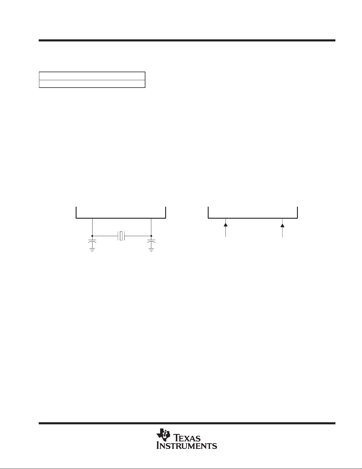
TMS320C242
ADVANCE
INFORMATION
DSP CONTROLLER
SPRS063B – DECEMBER 1997 – REVISED DECEMBER 1999
CLOCK CHARACTERISTICS AND TIMINGS
clock options
PARAMETER
PLL multiply-by-4
The ’C242 device includes an on-chip PLL which is hardwired for multiply-by-4 operation. This requires the use
of a 5-MHz clock input frequency for 20-MHz device operation. This input clock can be provided from either
an external reference crystal or oscillator.
external reference crystal clock option
The internal oscillator is enabled by connecting a crystal across XTAL1/CLKIN and XTAL2 pins as shown in
Figure 17a. The crystal should be in fundamental operation and parallel resonant, with an effective series
resistance of 30 Ω (typical)
20 pF.
external reference oscillator clock option
The internal oscillator is disabled by connecting a TTL-level clock signal to XT AL1/CLKIN and leaving the XTAL2
input pin unconnected as shown in Figure 17b.
†
and a power dissipation of 1 mW; it should be specified at a load capacitance of
XTAL2XTAL1/CLKIN XTAL1/CLKIN XTAL2
(see Note A)
C1
Crystal
C2
(see Note A)
External
Clock Signal
(toggling 0–5 V)
(a) (b)
NOTES: A. For the values of C1 and C2, see the crystal manufacturer’s specification.
B. TI recommends that customers have the resonator/crystal vendor characterize the operation of their device with the DSP chip. The
resonator/crystal vendor has the equipment and expertise to tune the tank circuit. The vendor can also advise customers regarding
the proper component values which ensure startup and stability over the entire operating range.
Figure 17. Recommended Crystal/Clock Connection
NC
†
If the input frequency is 5 MHz, the series resistances of the crystal can be between 30 to 150 Ω.
POST OFFICE BOX 1443 • HOUSTON, TEXAS 77251–1443
47
TMS320C242
ADVANCE
INFORMATION
DSP CONTROLLER
SPRS063B – DECEMBER 1997 – REVISED DECEMBER 1999
external reference crystal/clock with PLL circuit enabled
timings with the PLL circuit enabled
PARAMETER MIN TYP MAX UNIT
f
x
C1, C2 Load capacitance 10 pF
Input clock frequency
Oscillator/Resonator 1 5 MHz
CLKIN
1 5 MHz
switching characteristics over recommended operating conditions [H = 0.5 t
PARAMETER CLOCK MODE MIN TYP MAX UNIT
t
c(CO)
t
f(CO)
t
r(CO)
t
w(COL)
t
w(COH)
t
p
Cycle time, CLKOUT
Fall time, CLKOUT 4 ns
Rise time, CLKOUT 4 ns
Pulse duration, CLKOUT low H–3 H H+3 ns
Pulse duration, CLKOUT high H–3 H H+3 ns
Transition time, PLL synchronized after PLL enabled
before PLL lock,
CLKIN multiply by 4
50 ns
] (see Figure 18)
c(CO)
2500t
c(Cl)
timing requirements (see Figure 18)
EXTERNAL REFERENCE
CRYSTAL
t
c(Cl)
t
f(Cl)
t
r(Cl)
t
w(CIL)
t
w(CIH)
†
This device utilizes a fully static design and, therefore, can operate with input clock cycle time [t
characterized at frequencies approaching 0 Hz, but is tested at f
NOTE: Timings assume CLKOUT is set to output CPUCLK. CLKOUT is initialized to CPUCLK by power-on reset.Timings assume CLKOUT is
set to output CPUCLK. CLKOUT is initialized to CPUCLK by power-on reset.
Cycle time†, XTAL1/CLKIN
Fall time, XTAL1/CLKIN 5 ns
Rise time, XTAL1/CLKIN 5 ns
Pulse duration, XT AL1/CLKIN low as a percentage of t
Pulse duration, XTAL1/CLKIN high as a percentage of t
c(Cl)
c(Cl)
= 6.7 MHz to meet device test time requirements.
clk
5 MHz 200 ns
] approaching infinity. The device is
c(CI)
MIN MAX UNIT
40 60 %
40 60 %
ns
XTAL1/CLKIN
48
t
c(CI)
t
CLKOUT
t
c(CO)
w(CIH)
t
w(COH)
t
f(Cl)
t
w(COL)
t
w(CIL)
t
r(CO)
t
r(Cl)
t
f(CO)
t
f(CO)
Figure 18. CLKIN-to-CLKOUT Timing for PLL Oscillator Mode, Multiply-by-4 Option with 5-MHz Clock
POST OFFICE BOX 1443 • HOUSTON, TEXAS 77251–1443

low-power mode timings
Delay time, CLKOUT switching to
LPM2
ADVANCE
INFORMATION
TMS320C242
DSP CONTROLLER
SPRS063B – DECEMBER 1997 – REVISED DECEMBER 1999
switching characteristics over recommended operating conditions [H = 0.5t
(see Figure 19, Figure 20, and Figure 21)
PARAMETER LOW-POWER MODES MIN TYP MAX UNIT
t
d(WAKE-A)
t
d(IDLE-COH)
t
d(WAKE-OSC)
t
d(IDLE-OSC)
t
d(EX)
†
Timings assume CLKOUT is set to output CPUCLK. CLKOUT is initialized to CPUCLK by power-on reset.
A0–A15
CLKOUT
WAKE INT
‡
WAKE INT can be any valid interrupt or RESET
Delay time, CLKOUT switching to
program execution resume
Delay time, Idle instruction executed to CLKOUT high
Delay time, wakeup interrupt
asserted to oscillator running
Delay time, Idle instruction executed to oscillator power off
Delay time, reset vector executed
after RS
high
‡
IDLE1 LPM0 4 + 6 t
IDLE2 LPM1 4t
HALT
{PLL/OSC power down}
LPM2
t
d(WAKE–A)
36H ns
Figure 19. IDLE1 Entry and Exit Timing – LPM0
c(CO)
c(CO)
OSC start-up
and PLL lock
4t
c(CO)
c(CO)
time
†
]
15 t
c(CO)
ns
ns
ms
µs
A0–A15
CLKOUT
WAKE INT
‡
WAKE INT can be any valid interrupt or RESET
‡
Figure 20. IDLE2 Entry and Exit Timing – LPM1
A0–A15
t
d(IDLE–COH)
CLKOUT
RESET
t
d(IDLE–COH)
t
d(IDLE–OSC)
Figure 21. HALT Mode – LPM2
t
d(WAKE–A)
t
d(WAKE–OSC)
t
d(EX)
POST OFFICE BOX 1443 • HOUSTON, TEXAS 77251–1443
49

TMS320C242
ADVANCE
INFORMATION
DSP CONTROLLER
SPRS063B – DECEMBER 1997 – REVISED DECEMBER 1999
RS timings
switching characteristics over recommended operating conditions for a reset [H = 0.5t
(see Figure 22)
PARAMETER MIN MAX UNIT
t
w(RSL1)
t
d(EX)
†
The parameter t
XTAL1/
CLKIN
RS
CLKOUT
A0–A15
Pulse duration, RS low
Delay time, reset vector executed after RS high
w(RSL1)
refers to the time RS
timing requirements for a reset [H = 0.5t
t
w(RSL)
t
d(EX)
‡
The parameter t
Pulse duration, RS low
Delay time, reset vector executed after RS high
refers to the time RS
w(RSL)
†
t
w(RSL1)
‡
is an output.
t
d(EX)
Figure 22. Watchdog Reset Pulse
] (see Figure 23)
c(CO)
is an input.
8t
c(CO)
36H ns
MIN MAX UNIT
5 ns
36H ns
c(CO)
]
ns
CLKOUT
A0–A15
CLKOUT
A0–A15
§
The value of x depends on the reset condition as follows: PLL enabled: Assuming CLKIN is stable, x=PLL lock-up time. If the internal oscillator
is used, x=oscillator lock-up time + PLL lock-up time. In case of resets after power on reset, x=0 (i.e., t
XTAL1/
CLKIN
RS
XTAL1/
CLKIN
RS
t
w(RSL)
t
w(RSL)
§
+ x
Case A. Power-on reset
§
+ x
Case B. External reset after power-on
t
t
d(EX)
Figure 23. Reset Timing
d(EX)
w(RSL)
=8H ns only).
50
POST OFFICE BOX 1443 • HOUSTON, TEXAS 77251–1443

DSP CONTROLLER
ADVANCE
INFORMATION
SPRS063B – DECEMBER 1997 – REVISED DECEMBER 1999
XF, BIO, and MP/MC timings
switching characteristics over recommended operating conditions (see Figure 24)
PARAMETER MIN MAX UNIT
t
d(XF)
timing requirements (see Figure 24)
t
su(BIO)CO
t
h(BIO)CO
CLKOUT
Delay time, CLKOUT high to XF high/low
Setup time, BIO or MP/MC low before CLKOUT low
Hold time, BIO or MP/MC low after CLKOUT low
t
d(XF)
MIN MAX UNIT
TMS320C242
–3 7 ns
0 ns
19 ns
XF
BIO
MP/MC
t
su(BIO)CO
,
t
h(BIO)CO
Figure 24. XF and BIO Timing
POST OFFICE BOX 1443 • HOUSTON, TEXAS 77251–1443
51

TMS320C242
ADVANCE
INFORMATION
DSP CONTROLLER
SPRS063B – DECEMBER 1997 – REVISED DECEMBER 1999
TIMING EVENT MANAGER INTERFACE
PWM timings
PWM refers to PWM outputs on PWM1, PWM2, PWM3, PWM4, PWM5, PWM6, T1PWM, and T2PWM.
switching characteristics over recommended operating conditions for PWM timing
[H = 0.5t
t
w(PWM)
t
d(PWM)CO
†
PWM outputs may be 100%, 0%, or increments of t
†
] (see Figure 25)
c(CO)
PARAMETER MIN MAX UNIT
Pulse duration, PWM output high/low
Delay time, CLKOUT low to PWM output switching
c(CO)
2H+5 ns
with respect to the PWM period.
15 ns
timing requirements‡ [H = 0.5t
‡
] (see Figure 26)
c(CO)
t
w(TMRDIR)
t
w(TMRCLK)
t
wh(TMRCLK)
t
c(TMRCLK)
Parameter TMRDIR is equal to the pin TDIR, and parameter TMRCLK is equal to the pin TCLKIN.
CLKOUT
PWMx
Pulse duration, TMRDIR low/high
Pulse duration, TMRCLK low as a percentage of TMRCLK cycle time
Pulse duration, TMRCLK high as a percentage of TMRCLK cycle time
Cycle time, TMRCLK
t
d(PWM)CO
t
w(PWM)
Figure 25. PWM Output Timing
CLKOUT
MIN MAX UNIT
4H+5 ns
40 60 %
40 60 %
4 t
c(CO)
ns
52
TMRDIR
t
w(TMRDIR)
Figure 26. Capture/TMRDIR Timing
POST OFFICE BOX 1443 • HOUSTON, TEXAS 77251–1443

capture and QEP timings
ADVANCE
INFORMATION
CAP refers to CAP1/QEP0/IOPA3, CAP2/QEP1/IOPA4, and CAP3/IOPA5.
TMS320C242
DSP CONTROLLER
SPRS063B – DECEMBER 1997 – REVISED DECEMBER 1999
timing requirements [H = 0.5t
t
w(CAP)
CLKOUT
Pulse duration, CAP input low/high
CAPx
] (see Figure 27)
c(CO)
t
w(CAP)
Figure 27. Capture Input and QEP Timing
MIN MAX UNIT
4H +15 ns
POST OFFICE BOX 1443 • HOUSTON, TEXAS 77251–1443
53

TMS320C242
ADVANCE
INFORMATION
DSP CONTROLLER
SPRS063B – DECEMBER 1997 – REVISED DECEMBER 1999
interrupt timings
INT refers to NMI, XINT1, and XINT2/IO. PDP refers to PDPINT.
switching characteristics over recommended operating conditions (see Figure 28)
PARAMETER MIN MAX UNIT
t
hz(PWM)PDP
t
d(INT)
Delay time, PDPINT low to PWM to high-impedance state
Delay time, INT low/high to interrupt-vector fetch
10t
c(CO)
12 ns
ns
timing requirements [H = 0.5t
t
w(INT)
t
w(PDP)
CLKOUT
PDPINT
PWM
XINT1/XINT2/NMI
ADDRESS
c(CO)
Pulse duration, INT input low/high
Pulse duration, PDPINT input low
] (see Figure 28)
t
w(PDP)
t
hz(PWM)PDP
t
w(INT)
MIN MAX UNIT
2H+15 ns
4H+5 ns
t
d(INT)
Interrupt Vector
54
Figure 28. Power Drive Protection Interrupt Timing
POST OFFICE BOX 1443 • HOUSTON, TEXAS 77251–1443
DSP CONTROLLER
ADVANCE
INFORMATION
SPRS063B – DECEMBER 1997 – REVISED DECEMBER 1999
general-purpose input/output timings
switching characteristics over recommended operating conditions (see Figure 29)
PARAMETER MIN MAX UNIT
t
d(GPO)CO
t
r(GPO)
t
f(GPO)
Delay time, CLKOUT low to GPIO low/high All GPIOs 9ns
Rise time, GPIO switching low to high All GPIOs 8 ns
Fall time, GPIO switching high to low All GPIOs 6 ns
TMS320C242
timing requirements [H = 0.5t
t
w(GPI)
CLKOUT
CLKOUT
Pulse duration, GPI high/low
GPIO
] (see Figure 30)
c(CO)
t
d(GPO)CO
t
f(GPO)
t
Figure 29. General-Purpose Output Timing
MIN MAX UNIT
2H+15 ns
r(GPO)
GPIO
t
w(GPI)
Figure 30. General-Purpose Input Timing
POST OFFICE BOX 1443 • HOUSTON, TEXAS 77251–1443
55

TMS320C242
ADV ANCE
INFORMATION
DSP CONTROLLER
SPRS063B – DECEMBER 1997 – REVISED DECEMBER 1999
10-bit dual analog-to-digital converter (ADC)
The 10-bit ADC has a separate power bus for its analog circuitry . These pins are referred to as V
CCA
and V
The power bus isolation is to enhance ADC performance by preventing digital switching noise of the logic
circuitry that can be present on VSS and VCC from coupling into the ADC analog stage. All ADC specifications
are given with respect to V
unless otherwise noted.
SSA
Resolution 10-bit (1024 values). . . . . . . . . . . . . . . . . . . . . . . . . . . . . . . . . . . . . . . . . . . . . . . . . . . . . . . . . . . . . . . . . .
Monotonic Assured. . . . . . . . . . . . . . . . . . . . . . . . . . . . . . . . . . . . . . . . . . . . . . . . . . . . . . . . . . . . . . . . . . . . . . . . . . . . .
Output conversion mode 000h to 3FFh (000h for VI ≤ V
; 3FFh for VI ≥ V
SSA
Conversion time (including sample time) 1 ms. . . . . . . . . . . . . . . . . . . . . . . . . . . . . . . . . . . . . . . . . . . . . . . . . . . . .
recommended operating conditions
MIN NOM MAX UNIT
V
V
V
V
V
†
V
CCA
SSA
REFHI
REFLO
AI
REFHI
Analog supply voltage 4.5 5 5.5 V
Analog ground 0 V
Analog supply reference source
Analog ground reference source
Analog input voltage, ADCIN00–ADCIN07 V
and V
must be stable, within ±1/2 LSB of the required resolution, during the entire conversion time.
REFLO
†
†
V
REFLO
V
SSA
SSA
V
V
REFHI
V
CCA
CCA
ADC operating frequency
MIN MAX UNIT
ADC operating frequency 20 MHz
SSA
CCA
V
V
V
.
). . . . . . . . . . . . . . . . . . . . . . .
56
POST OFFICE BOX 1443 • HOUSTON, TEXAS 77251–1443

TMS320C242
I
Anal
Ty ical ca acitive load on
ADVANCE
INFORMATION
DSP CONTROLLER
SPRS063B – DECEMBER 1997 – REVISED DECEMBER 1999
operating characteristics over recommended operating condition ranges
PARAMETER DESCRIPTION MIN MAX UNIT
V
= 5.5 V
pp
CCA
C
ai
E
DNL
E
INL
t
d(PU)
Z
AI
†
Absolute resolution = 4.89 mV . At V
decreases. Therefore, the absolute accuracy and differential/integral linearity errors in terms of LSBs increase.
og supply current
Analog input capacitance
Differential nonlinearity error
Integral nonlinearity error
Delay time, power-up to ADC valid Time to stabilize analog stage after power-up 10 ms
Analog input source impedance
= 5 V and V
REFHI
REFLO
CCA
V
= V
CCA
Typical capacitive load on
analog input pin
Difference between the actual step width and the ideal
value
Maximum deviation from the best straight line through
the ADC transfer characteristics, excluding the
quantization error
Analog input source impedance for conversions to
remain within specifications
= 0 V , this is one LSB. As V
REFHI
= 5.5 V
REFHI
Converting 10
Non-converting 2
PLL or OSC power
down
Non-sampling 10
Sampling 30
decreases, V
†
increases, or both, the LSB size
REFLO
ADC input pin circuit
One of the most common A/D application errors is inappropriate source impedance. In practice, minimum
source impedance should be used to limit the error as well as to minimize the required sampling time; however ,
the source impedance must be smaller than ZAI. A typical ADC input pin circuit is shown in Figure 31.
mA
1 mA
pF
2 LSB
2 LSB
10 Ω
R
equiv
R1
V
IN
R1 = 10 Ω typical
(to ADCINx input)
V
AI
Figure 31. Typical ADC Input Pin Circuit
POST OFFICE BOX 1443 • HOUSTON, TEXAS 77251–1443
57

TMS320C242
ADVANCE
INFORMATION
DSP CONTROLLER
SPRS063B – DECEMBER 1997 – REVISED DECEMBER 1999
internal ADC module timings (see Figure 32)
MIN MAX UNIT
t
c(AD)
t
w(SHC)
t
w(SH)
t
w(C)
t
d(SOC-SH)
t
d(EOC-FIFO)
t
d(ADCINT)
†
The total sample/hold and conversion time is determined by the summation of t
‡
Start of conversion is signaled by the ADCIMSTAR T bit (ADCTRL1.13) or the ADCSOC bit (ADCTRL1.0) set in software, the external start signal
active (ADCSOC), or internal EVSOC signal active.
Bit Converted
ADC Clock
Cycle time, ADC prescaled clock 50 ns
Pulse duration, total sample/hold and conversion time
Pulse duration, sample and hold time 3t
Pulse duration, total conversion time 10t
Delay time, start of conversion‡ to beginning of sample and hold 3t
Delay time, end of conversion to data loaded into result FIFO 2t
Delay time, ADC flag to ADC interrupt 2t
t
c(AD)
9
†
, t
), t
d(SOC-SH)
678
451
w(SH
2
03
w(C)
, and t
900 ns
c(AD)
c(AD)
c(CO)
c(CO)
c(CO)
d(EOC-FIFO)
ns
ns
ns
ns
ns
.
Start of Convert
Analog Input
EOC/Convert
Internal Start/
Sample Hold
XFR to FIFO
t
w(C)
t
w(SH)
t
d(SOC–SH)
t
d(EOC–FIFO)
t
w(SHC)
t
d(ADCINT)
Figure 32. Analog-to-Digital Internal Module Timing
58
POST OFFICE BOX 1443 • HOUSTON, TEXAS 77251–1443

ADVANCE
INFORMATION
TMS320C242
DSP CONTROLLER
SPRS063B – DECEMBER 1997 – REVISED DECEMBER 1999
register file compilation
Table 14 is a collection of all the programmable registers of the TMS320x24x (provided for a quick reference).
Table 14. Register File Compilation
ADDR BIT 15 BIT 14 BIT 13 BIT 12 BIT 11 BIT 10 BIT 9 BIT 8 REG
BIT 7 BIT 6 BIT 5 BIT 4 BIT 3 BIT 2 BIT 1 BIT 0
DA TA MEMORY SPACE
CPU STATUS REGISTERS
ARP OV OVM 1 INTM DP(8)
DP(7) DP(6) DP(5) DP(4) DP(3) DP(2) DP(1) DP(0)
ARB CNF TC SXM C 1
1 1 1 XF 1 1 PM
GLOBAL MEMORY AND CPU INTERRUPT REGISTERS
00004h
00005h
00006h
07010h Reserved PIRQR0
0701 1h Reserved PIRQR1
07012h
to
07013h
07014h Reserved PIACKR0
07015h Reserved PIACKR1
07016h
to
07017h
07018h
07019h
to
0701Bh
0701Ch
0701Dh Reserved
0701Eh
0701Fh Reserved
07020h
to
07022h
— — — — — — — —
—
— — — — — — — —
— — — — — — — —
—
— CLKSRC LPM1 LPM0 — — — —
—
DIN15 DIN14 DIN13 DIN12 DIN11 DIN10 DIN9 DIN8
DIN7
V15 V14 V13 V12 V11 V10 V9 V8
V7
— INT6 MASK INT5 MASK INT4 MASK INT3 MASK INT2 MASK INT1 MASK
Global Data Memory Configuration Bits (7–0)
— INT6 FLAG INT5 FLAG INT4 FLAG INT3 FLAG INT2 FLAG INT1 FLAG
SYSTEM REGISTERS
Reserved
Reserved
— — — — — — ILLADR
Reserved
DIN6 DIN5 DIN4 DIN3 DIN2 DIN1 DIN0
V6 V5 V4 V3 V2 V1 V0
WD CONTROL REGISTERS
Reserved
ST0
ST1
IMR
GREG
IFR
SCSR
DINR
PIVR
POST OFFICE BOX 1443 • HOUSTON, TEXAS 77251–1443
59

TMS320C242
07032h
ADCTRL1
ADVANCE
INFORMATION
DSP CONTROLLER
SPRS063B – DECEMBER 1997 – REVISED DECEMBER 1999
register file compilation (continued)
ADDR BIT 15 BIT 14 BIT 13 BIT 12 BIT 11 BIT 10 BIT 9 BIT 8 REG
07023h D7 D6 D5 D4 D3 D2 D1 D0 WDCNTR
07024h Reserved
07025h D7 D6 D5 D4 D3 D2 D1 D0 WDKEY
07026h
07028h
07029h WD FLAG WDDIS WDCHK2 WDCHK1 WDCHK0 WDPS2 WDPS1 WDPS0 WDCR
0702Ah
0702Ch
0702Dh
07031h
07032h
07033h Reserved
07034h
07035h Reserved
07036h
07037h Reserved
07038h
07039h
0703Fh
07040h
0704Fh
07050h
07051h —
07052h
07053h BAUD7 BAUD6 BAUD5 BAUD4 BAUD3 BAUD2 BAUD1
07054h TXRDY TX EMPTY — — — —
07055h RX ERROR RXRDY BRKDT FE OE PE RXWAKE — SCIRXST
07056h ERXDT7 ERXDT6 ERXDT5 ERXDT4 ERXDT3 ERXDT2 ERXDT1 ERXDT0 SCIRXEMU
07057h RXDT7 RXDT6 RXDT5 RXDT4 RXDT3 RXDT2 RXDT1 RXDT0 SCIRXBUF
07058h Reserved
Table 14. Register File Compilation (Continued)
BIT 7 BIT 6 BIT 5 BIT 4 BIT 3 BIT 2 BIT 1 BIT 0
WD CONTROL REGISTERS (CONTINUED)
ENA
Reserved
Reserved
Reserved
Reserved
Reserved
ADDR/IDLE
MODE
ADCCON-
RUN
ADCEVSOC
SCI
CHAR2
ADCINTEN ADCINTFLAG
ADCEXTSOC —
SCI
CHAR1
RX/BK
INT ENA
to
to
to
A-to-D MODULE CONTROL REGISTERS
SUSPEND-
SOFT
ADCEOC ADC2CHSEL ADC1CHSEL ADCSOC
— —
D9 D8 D7 D6 D5 D4 D3 D2
D1
D9 D8 D7 D6 D5 D4 D3 D2
D1
to
to
STOP
BITS
BAUD15
(MSB)
SUSPEND-
FREE
ADCFIFO2
D0 0 0 0 0 0 0
D0 0 0 0 0 0 0
SERIAL COMMUNICATIONS INTERFACE (SCI) CONFIGURATION CONTROL REGISTERS
EVEN/ODD
PARITY
RX ERR
INT ENA
BAUD14 BAUD13 BAUD12 BAUD11 BAUD10 BAUD9 BAUD8 SCIHBAUD
ADCIM-
START
EVSOCP
— ADCFIFO1 ADCPSCALE
PARITY
ENABLE
SW RESET — TXWAKE SLEEP TXENA RXENA SCICTL1
ADC2EN ADC1EN
EXTSOCP INTPRI
LOOP BACK
SCI
CHAR0
BAUD0
(LSB)
TX
INT ENA
ADCTRL1
ADCTRL2
ADCFIFO1
ADCFIFO2
SCICCR
SCILBAUD
SCICTL2
60
POST OFFICE BOX 1443 • HOUSTON, TEXAS 77251–1443

ADVANCE
INFORMATION
TMS320C242
DSP CONTROLLER
SPRS063B – DECEMBER 1997 – REVISED DECEMBER 1999
register file compilation (continued)
Table 14. Register File Compilation (Continued)
ADDR BIT 15 BIT 14 BIT 13 BIT 12 BIT 11 BIT 10 BIT 9 BIT 8 REG
BIT 7 BIT 6 BIT 5 BIT 4 BIT 3 BIT 2 BIT 1 BIT 0
SERIAL COMMUNICATIONS INTERF ACE (SCI) CONFIGURATION CONTROL REGISTERS (CONTINUED)
07059h TXDT7 TXDT6 TXDT5 TXDT4 TXDT3 TXDT2 TXDT1 TXDT0 SCITXBUF
0705Ah
to
0705Eh
0705Fh —
07060h
to
0706Fh
XINT1
07070h
07071h
07072h
to
0708Fh
07090h
07091h Reserved
07092h
07093h
to
07097h
07098h
07099h Reserved
0709Ah
0709Bh Reserved
0709Ch
0709Dh Reserved
0709Eh Reserved
0709Fh Reserved
07100h
to
073FFh
FLAG
— — — — —
XINT2
FLAG
— — — — —
CRA.15 CRA.14 CRA.13 CRA.12 CRA.11 CRA.10 CRA.9 CRA.8
CRA.7
— — — — — — CRB.9 CRB.8
—
A7DIR A6DIR A5DIR A4DIR A3DIR A2DIR A1DIR A0DIR
IOPA7
B7DIR B6DIR B5DIR B4DIR B3DIR B2DIR B1DIR B0DIR
IOPB7
C7DIR C6DIR C5DIR C4DIR C3DIR C2DIR C1DIR C0DIR
IOPC7
SCITX
PRIORITY
— — — — — — —
— — — — — — —
CRA.6 CRA.5 CRA.4 CRA.3 CRA.2 CRA.1 CRA.0
— — — — — CRB.1 CRB.0
IOPA6 IOPA5 IOPA4 IOPA3 IOPA2 IOPA1 IOPA0
IOPB6 IOPB5 IOPB4 IOPB3 IOPB2 IOPB1 IOPB0
IOPC6 IOPC5 IOPC4 IOPC3 IOPC2 IOPC1 IOPC0
SCIRX
PRIORITY
EXTERNAL INTERRUPT CONTROL REGISTERS
DIGITAL I/O CONTROL REGISTERS
SCI
SOFT
Reserved
Reserved
Reserved
Reserved
Reserved
SCI
FREE
— — — SCIPRI
XINT1
POLARITY
XINT2
POLARITY
XINT1
PRIORITY
XINT2
PRIORITY
D1DIR D0DIR
IOPD1 IOPD0
XINT1
XINT2
ENA
ENA
XINT1CR
XINT2CR
OCRA
OCRB
PADATDIR
PBDATDIR
PCDATDIR
PDDATDIR
POST OFFICE BOX 1443 • HOUSTON, TEXAS 77251–1443
61

TMS320C242
ADVANCE
INFORMATION
DSP CONTROLLER
SPRS063B – DECEMBER 1997 – REVISED DECEMBER 1999
register file compilation (continued)
07230h
073FFh
07400h
07401h
07402h
07403h
07404h
07405h
07406h
07407h
07408h
07409h
07410h
07411h
07412h Reserved
07413h
07414h Reserved
07415h
07416h Reserved
07417h
07418h
07419h
0741Ah
0741Fh
Table 14. Register File Compilation (Continued)
ADDR BIT 15 BIT 14 BIT 13 BIT 12 BIT 11 BIT 10 BIT 9 BIT 8 REG
BIT 7 BIT 6 BIT 5 BIT 4 BIT 3 BIT 2 BIT 1 BIT 0
to
to
to
GENERAL-PURPOSE (GP) TIMER CONFIGURATION CONTROL REGISTERS
— T2STAT T1STAT — T2TOADC T1TOADC(1)
T1TOADC(0)
D15 D14 D13 D12 D11 D10 D9 D8
D7
D15 D14 D13 D12 D11 D10 D9 D8
D7
D15 D14 D13 D12 D11 D10 D9 D8
D7
FREE SOFT — TMODE1 TMODE0 TPS2 TPS1 TPS0
TSWT1
D15 D14 D13 D12 D11 D10 D9 D8
D7
D15 D14 D13 D12 D11 D10 D9 D8
D7
D15 D14 D13 D12 D11 D10 D9 D8
D7
FREE SOFT — TMODE1 TMODE0 TPS2 TPS1 TPS0
TSWT1
CENABLE CLD1 CLD0 SVENABLE ACTRLD1 ACTRLD0 FCOMPOE —
—
SVRDIR D2 D1 D0 CMP6ACT1 CMP6ACT0 CMP5ACT1 CMP5ACT0
CMP4ACT1
— — — — DBT3 DBT2 DBT1 DBT0
EDBT3
D15 D14 D13 D12 D11 D10 D9 D8
D7
D15 D14 D13 D12 D11 D10 D9 D8
D7
D15 D14 D13 D12 D11 D10 D9 D8
D7
TCOMPOE — T2PIN T1PIN
D6 D5 D4 D3 D2 D1 D0
D6 D5 D4 D3 D2 D1 D0
D6 D5 D4 D3 D2 D1 D0
TENABLE TCLKS1 TCLKS0 TCLD1 TCLD0 TECMPR SELT1PR
D6 D5 D4 D3 D2 D1 D0
D6 D5 D4 D3 D2 D1 D0
D6 D5 D4 D3 D2 D1 D0
TENABLE TCLKS1 TCLKS0 TCLD1 TCLD0 TECMPR SELT1PR
FULL AND SIMPLE COMPARE UNIT REGISTERS
— — — — — — —
CMP4ACT0 CMP3ACT1 CMP3ACT0 CMP2ACT1 CMP2ACT0 CMP1ACT1 CMP1ACT0
EDBT2 EDBT1 DBTPS2 DBTPS1 DBTPS0 — —
D6 D5 D4 D3 D2 D1 D0
D6 D5 D4 D3 D2 D1 D0
D6 D5 D4 D3 D2 D1 D0
Reserved
GPTCON
T1CNT
T1CMPR
T1PR
T1CON
T2CNT
T2CMPR
T2PR
T2CON
Reserved
COMCON
ACTR
DBTCON
CMPR1
CMPR2
CMPR3
Reserved
62
POST OFFICE BOX 1443 • HOUSTON, TEXAS 77251–1443

ADVANCE
INFORMATION
TMS320C242
DSP CONTROLLER
SPRS063B – DECEMBER 1997 – REVISED DECEMBER 1999
register file compilation (continued)
Table 14. Register File Compilation (Continued)
ADDR BIT 15 BIT 14 BIT 13 BIT 12 BIT 11 BIT 10 BIT 9 BIT 8 REG
BIT 7 BIT 6 BIT 5 BIT 4 BIT 3 BIT 2 BIT 1 BIT 0
CAPTURE UNIT REGISTERS
07420h
07421h Reserved
07422h
07423h
07424h
07425h
07426h Reserved
07427h
07428h
07429h
0742Ah
to
0742Bh
0742Ch
0742Dh
0742Eh
0742Fh
07430h
07431h
07432h
to
0743Fh
CAPRES CAPQEPN CAP3EN — CAP3TSEL CAP12TSEL CAP3TOADC
CAP1EDGE
— CAP3FIFO CAP2FIFO CAP1FIFO
—
D15 D14 D13 D12 D11 D10 D9 D8
D7
D15 D14 D13 D12 D11 D10 D9 D8
D7
D15 D14 D13 D12 D11 D10 D9 D8
D7
D15 D14 D13 D12 D11 D10 D9 D8
D7
D15 D14 D13 D12 D11 D10 D9 D8
D7
D15 D14 D13 D12 D11 D10 D9 D8
D7
— — — — —
T1PINT
ENA
— — — — — — — —
—
— — — — — — — —
—
— — — — —
T1PINT
FLAG
— — — — — — — —
—
— — — — — — — —
—
— — — — — — —
D6 D5 D4 D3 D2 D1 D0
D6 D5 D4 D3 D2 D1 D0
D6 D5 D4 D3 D2 D1 D0
D6 D5 D4 D3 D2 D1 D0
D6 D5 D4 D3 D2 D1 D0
D6 D5 D4 D3 D2 D1 D0
— — —
— — —
— — — —
— — —
— — —
— — — —
CAP2EDGE CAP3EDGE —
Reserved
EVENT MANAGER (EV) INTERRUPT CONTROL REGISTERS
T1OFINT
ENA
CMP3INT
ENA
T2OFINT
ENA
CMP3INT
FLAG
T2OFINT
FLAG
Reserved
CMP2INT
ENA
T2UFINT
ENA
CAP3INT
ENA
T1OFINT
FLAG
CMP2INT
FLAG
T2UFINT
FLAG
CAP3INT
FLAG
T1UFINT
ENA
CMP1INT
ENA
T2CINT
ENA
CAP2INT
ENA
T1UFINT
FLAG
CMP1INT
FLAG
T2CINT
FLAG
CAP2INT
FLAG
T1CINT
ENA
PDPINT
ENA
T2PINT
ENA
CAP1INT
ENA
T1CINT
FLAG
PDPINT
FLAG
T2PINT
FLAG
CAP1INT
FLAG
CAPCON
CAPFIFO
CAP1FIFO
CAP2FIFO
CAP3FIFO
CAP1FBOT
CAP2FBOT
CAP3FBOT
EVIMRA
EVIMRB
EVIMRC
EVIFRA
EVIFRB
EVIFRC
POST OFFICE BOX 1443 • HOUSTON, TEXAS 77251–1443
63
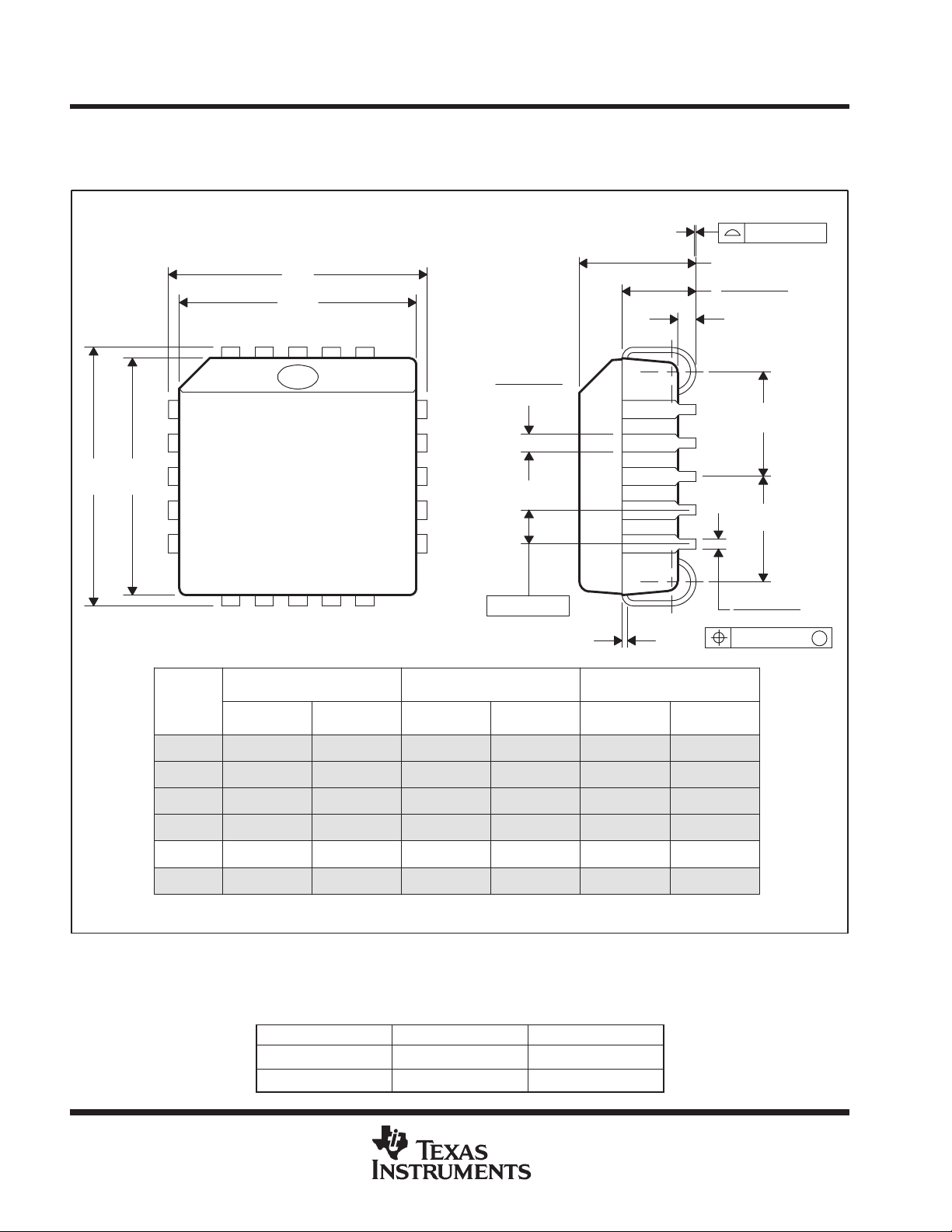
TMS320C242
ADVANCE
INFORMATION
DSP CONTROLLER
SPRS063B – DECEMBER 1997 – REVISED DECEMBER 1999
MECHANICAL DATA
FN (S-PQCC-J**) PLASTIC J-LEADED CHIP CARRIER
20 PIN SHOWN
Seating Plane
0.004 (0,10)
D
D1
13
4
E1E
8
9
NO. OF
PINS
**
D/E
19
13
18
14
0.032 (0,81)
0.026 (0,66)
0.050 (1,27)
0.008 (0,20) NOM
D1/E1
MINMAXMIN
MAX
D2/E2
MIN
0.180 (4,57) MAX
0.120 (3,05)
0.090 (2,29)
0.020 (0,51) MIN
D2/E2
D2/E2
0.021 (0,53)
0.013 (0,33)
0.007 (0,18)
MAX
M
NOTES: A. All linear dimensions are in millimeters.
64
20
28
44
52
68
84
B. This drawing is subject to change without notice.
C. Falls within JEDEC MS-018
0.385 (9,78)
0.485 (12,32)
0.685 (17,40)
0.785 (19,94)
0.985 (25,02)
1.185 (30,10)
0.395 (10,03)
0.495 (12,57)
0.695 (17,65)
0.795 (20,19)
0.995 (25,27)
1.195 (30,35)
Typical Thermal Resistance Characteristics
PARAMETER DESCRIPTION °C/W
Θ
JA
Θ
JC
POST OFFICE BOX 1443 • HOUSTON, TEXAS 77251–1443
0.350 (8,89)
0.450 (11,43)
0.650 (16,51)
0.750 (19,05)
0.950 (24,13)
1.150 (29,21)
Junction-to-ambient 48
Junction-to-case 11
0.356 (9,04)
0.456 (11,58)
0.656 (16,66)
0.756 (19,20)
0.958 (24,33)
1.158 (29,41)
0.541 (13,74)
0.141 (3,58)
0.191 (4,85)
0.291 (7,39)
0.341 (8,66)
0.441 (11,20)
0.169 (4,29)
0.219 (5,56)
0.319 (8,10)
0.369 (9,37)
0.469 (11,91)
0.569 (14,45)
4040005/B 03/95

TMS320C242
ADVANCE
INFORMATION
DSP CONTROLLER
SPRS063B – DECEMBER 1997 – REVISED DECEMBER 1999
MECHANICAL DATA
PG (R-PQFP-G64) PLASTIC QUAD FLATPACK
52
64
51
1,00
1
18,00 TYP
20,20
19,80
24,40
23,60
0,45
0,25
33
19
0,20
M
32
20
12,00 TYP
18,0014,20
13,80 17,20
0,15 NOM
Gage Plane
2,70 TYP
3,10 MAX
NOTES: A. All linear dimensions are in millimeters.
B. This drawing is subject to change without notice.
C. Contact field sales office to determine if a tighter coplanarity requirement is available for this package.
Typical Thermal Resistance Characteristics
PARAMETER DESCRIPTION °C/W
Θ
JA
Θ
JC
0,10 MIN
Junction-to-ambient 35
Junction-to-case 11
0,25
0°–ā10°
1,10
0,70
Seating Plane
0,10
4040101/B 03/95
POST OFFICE BOX 1443 • HOUSTON, TEXAS 77251–1443
65

IMPORTANT NOTICE
T exas Instruments and its subsidiaries (TI) reserve the right to make changes to their products or to discontinue
any product or service without notice, and advise customers to obtain the latest version of relevant information
to verify, before placing orders, that information being relied on is current and complete. All products are sold
subject to the terms and conditions of sale supplied at the time of order acknowledgement, including those
pertaining to warranty, patent infringement, and limitation of liability.
TI warrants performance of its semiconductor products to the specifications applicable at the time of sale in
accordance with TI’s standard warranty. Testing and other quality control techniques are utilized to the extent
TI deems necessary to support this warranty . Specific testing of all parameters of each device is not necessarily
performed, except those mandated by government requirements.
CERTAIN APPLICATIONS USING SEMICONDUCTOR PRODUCTS MAY INVOLVE POTENTIAL RISKS OF
DEATH, PERSONAL INJURY, OR SEVERE PROPERTY OR ENVIRONMENTAL DAMAGE (“CRITICAL
APPLICATIONS”). TI SEMICONDUCTOR PRODUCTS ARE NOT DESIGNED, AUTHORIZED, OR
WARRANTED TO BE SUITABLE FOR USE IN LIFE-SUPPORT DEVICES OR SYSTEMS OR OTHER
CRITICAL APPLICA TIONS. INCLUSION OF TI PRODUCTS IN SUCH APPLICATIONS IS UNDERST OOD TO
BE FULLY AT THE CUSTOMER’S RISK.
In order to minimize risks associated with the customer’s applications, adequate design and operating
safeguards must be provided by the customer to minimize inherent or procedural hazards.
TI assumes no liability for applications assistance or customer product design. TI does not warrant or represent
that any license, either express or implied, is granted under any patent right, copyright, mask work right, or other
intellectual property right of TI covering or relating to any combination, machine, or process in which such
semiconductor products or services might be or are used. TI’s publication of information regarding any third
party’s products or services does not constitute TI’s approval, warranty or endorsement thereof.
Copyright 1999, Texas Instruments Incorporated
 Loading...